J. Semicond.
Volume 47, Issue 2, Feb 2026


Call for Papers
Focus Collection on Pathways to Advanced Flexible Electronics: Materials, Structures, and Systems
Guest Editors: Rongrong Bao, Desheng Kong, La Li, Chunfeng Wang, Yue Liu

Call for Papers
Special Issue on Optoelectronic Neuromorphic Devices
Guest Editors: Zhenyi Ni, Zhongqiang Wang, Jia Huang, Xiaodong Pi

Call for Papers
Special Issue on Flexible and Smart Electronics for Sensors 4.0
Guest Editors: Zhuoran Wang, Yang Li, Qilin Hua

Call for Papers
Towards High Performance Ga2O3 Electronics: Epitaxial Growth and Power Devices
Guest Editors: Genquan Han, Shibing Long, Yuhao Zhang, Yibo Wang

Call for Papers
Novel Semiconductor-Biochemical Sensors
Guest Editors: Zhao Li, Xiangmei Lin, Dongxian He, Yingxin Ma, Yuanjing Lin

Special Issue
Flexible Energy Devices
Guest Edited: Zhiyong Fan, Yonghua Chen, Yuanjing Lin, Yunlong Zi, Hyunhyub Ko, Qianpeng Zhang

Special Issue
Semiconductor Optoelectronic Integrated Circuits
Guest Edited: Wei Wang, Lingjuan Zhao, Dan Lu, Jianping Yao, Weiping Huang, Yong Liu, Brent Little

Special Issue
Beyond Moore: Three-Dimensional (3D) Heterogeneous Integration
Guest Edited: Yue Hao, Huaqiang Wu, Yuchao Yang, Qi Liu, Xiao Gong, Genquan Han, Ming Li

Special Issue
Beyond Moore: Resistive Switching Devices for Emerging Memory and Neuromorphic Computing
Guest Edited: Yue Hao, Huaqiang Wu, Yuchao Yang, Qi Liu, Xiao Gong, Genquan Han, Ming Li

Special Issue
Celebration of the 60th Anniversary of Dedicating to Scientific Research of Prof. Zhanguo Wang
Guest Editors: Zhijie Wang, Chao Zhao , Fei Ding

Special Issue
Reconfigurable Computing for Energy Efficient AI Microchip Technologies
Guest Editors: Haigang Yang, Yajun Ha, Lingli Wang, Wei Zhang, Yingyan Lin


Special Issue
Semiconductor Materials Genome Initiative: New Concepts and Discoveries
Guest Editors: Suhuai Wei, Junwei Luo, Bing Huang

Special Issues
2D-materials-related physical properties and optoelectronic devices
Guest Editors: Ping-Heng Tan, Lijun Zhang, Lun Dai, Shuyun Zhou

Special Issue
Flexible and Wearable Sensors for Robotics and Health
Guest Editors: Zhiyong Fan, Johnny C. Ho, Chuan Wang, Yun-Ze Long, Huan Liu


Special Issue
Si-Based Materials and Devices
Guest Editors: Chuanbo Li, Linwei Yu, Jinsong Xia

Special Issue
Devices and Circuits for Wearable and IoT Systems
Guest Editors: Zhihua Wang, Yong Hei, Zhangming Zhu

Special Issue
Flexible and Wearable Electronics: from Materials to Applications
Guest Editors: Guozhen Shen, Yongfeng Mei, Chuan Wang, Taeyoon Lee

News
First time: Science Cites Journal of Semiconductors

News
JOS has been indexed in ESCI database since 2016
 Abstract
 Full Text
 PDF
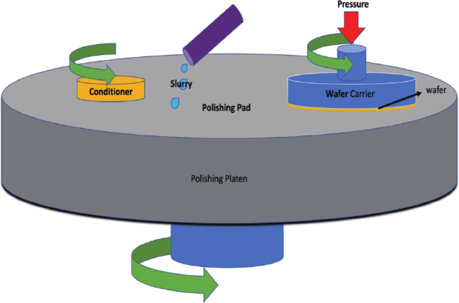
Chemical mechanical polishing (CMP) serves as an indispensable process for achieving global planarization in semiconductor manufacturing, especially as integrated circuit (IC) technology advances to sub-7 nm nodes, where atomic-level surface flatness becomes crucial. Silica abrasives, which account for over 90% of the abrasive market in advanced CMP processes, operate not through simple mechanical grinding but through a key "chemical-mechanical synergistic" mechanism: chemically softening the wafer surface, then mechanically removing the softened layer to expose a new surface, which is further softened and removed, repeating this cycle to produce a smooth wafer. Despite their prevalence, conventional silica abrasives still face challenges, including relatively low material removal rate (MRR), a tendency to agglomerate, leading to poor dispersion and surface defects, and limitations in achieving ultimate surface uniformity. Significant progress has been made to address these issues. Development has progressed from simple spherical particles to complex structural designs (such as mesoporous, hollow, and raspberry-shaped structures) to enhance slurry transport and mechanical action. Surface chemical modifications (e.g., using amino or polymer groups) can improve dispersion stability and reduce scratching. Furthermore, composites with other materials (e.g., ceria, polymers) and precise control of particle size distribution are key to enhancing performance. These innovative approaches have yielded significant performance gains. State-of-the-art slurries have demonstrated the ability to achieve surface roughness below 0.1 nm rms. The development of silica abrasives is increasingly focused on sustainability and smart manufacturing. A prominent direction is the design of biodegradable abrasives that disintegrate after use, thereby simplifying post-chemical mechanical polishing (CMP) cleanup and minimizing environmental impact—an approach fully aligned with green manufacturing principles. This review systematically summarizes the progress of silica abrasives for CMP over the past 60 years. This summary provides theoretical insights and forward-looking strategies to overcome the current limitations of abrasive technology. We believe this review will be helpful in advancing the field of CMP abrasives towards next-generation semiconductor manufacturing.
 Abstract
 Full Text
 PDF
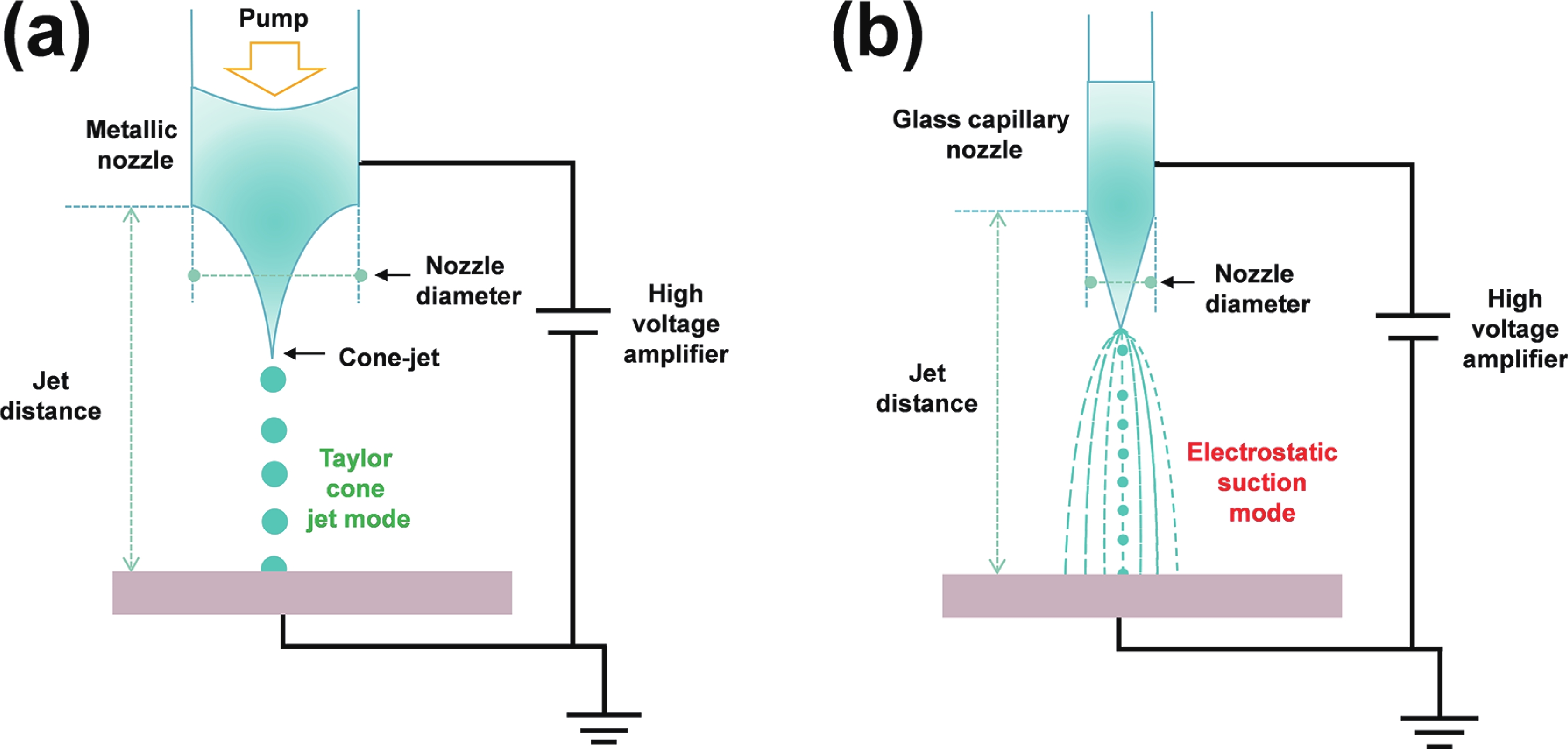
Electrohydrodynamic (EHD) inkjet printing has emerged as a powerful micro-/nanofabrication technique for high-resolution perovskite quantum dot (PeQD) color-conversion layers, offering precise control over pixel morphology, dimensions, and composition. This review systematically examines the mechanisms of cone-jet and electrostatic-attraction modes in EHD printing, highlighting recent advances in PeQD ink design, solvent and ligand engineering, and printing parameter optimization. Perovskite precursor and colloidal inks are discussed in detail, emphasizing strategies to enhance droplet ejection stability, suppress coffee-ring effects, and achieve uniform, high-luminescence pixels. Ligand exchange, dual-ligand passivation, and core−shell or polymer encapsulation are shown to effectively mitigate ion migration, surface defects, and environmental degradation, thereby improving photoluminescence efficiency and stability. Multi-channel and multi-nozzle EHD printing systems enable dynamic halide composition control and parallel RGB pixel deposition, facilitating ultrahigh-resolution patterning down to submicron feature sizes. Finally, the review highlights future directions, including synergistic PeQD material synthesis, advanced ink formulation, scalable high-throughput printing, and integration of PeQD color-conversion pixels into full-color micro-LED displays with minimal crosstalk and robust operational stability. These developments collectively demonstrate the immense potential of EHD inkjet printing for next-generation high-performance display technologies.
 Abstract
 Full Text
 PDF
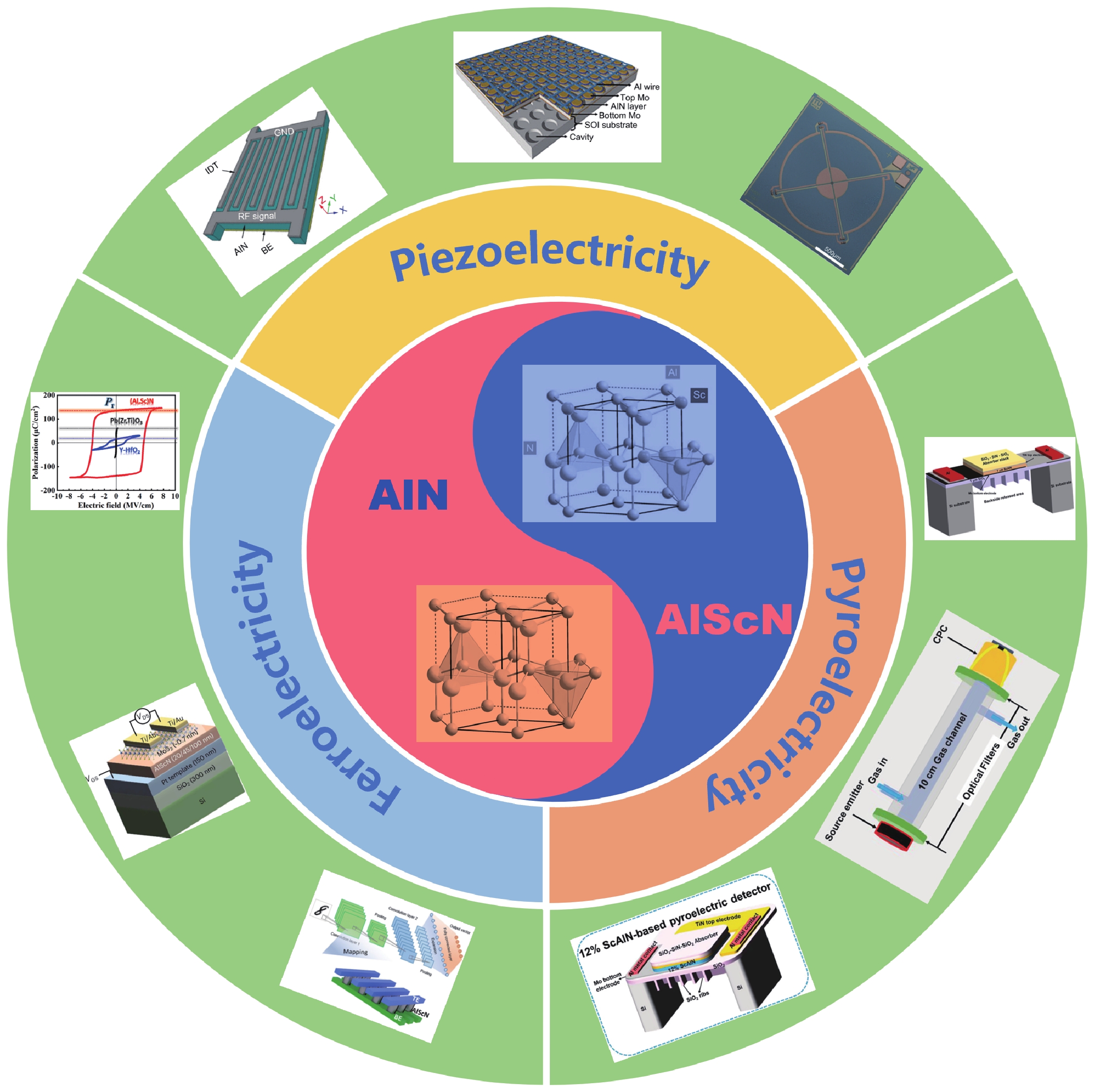
Aluminum scandium nitride (AlScN), an emerging Ⅲ-nitride semiconductor material, has attracted significant attention in recent years due to its exceptional piezoelectric properties, high thermal stability, tunable bandgap, and excellent compatibility with micro/nano fabrication. This paper systematically reviews the crystal structure, fundamental properties, and property modulation mechanisms of AlScN. It also summarizes recent progress in micro/nano fabrication technologies, including deposition, etching, and device integration. Furthermore, the applications of AlScN in diverse fields such as micro-electromechanical systems (MEMS), RF communications, energy conversion, optoelectronics and sensors are discussed. Finally, current challenges and promising future research directions for AlScN are outlined.
 Abstract
 Full Text
 PDF
Significant progress has been achieved in the field of organic solar cells (OSCs). Most devices with power conversion efficiencies (PCEs) exceeding 20% rely predominantly on active materials that incorporate D18 or its derivatives as the donor. In contrast, the PCEs over 20% have been realized as well for OSCs with the non-D18-based donor materials by simultaneously optimizing material properties, active layer morphologies and interface engineering, thereby demonstrating the potential to outperform D18 counterparts. Therefore, this review summarizes an overview of recent advancements in OSCs with the PCEs over 20% utilizing the non-D18-based donor materials, and highlights three critical aspects including molecular design strategies, the active layer morphologies, and the interface optimization. Their synergistic roles are advantageous in enhancing the exciton dissociation, facilitating the charge transport, and suppressing the recombination losses, accordingly supporting the improved PCEs over 20%. Furthermore, the challenges and valuable insights are discussed, which can lead to improved efficiency, scalable fabrication, and enhanced environmental and thermal stability, potentially accelerating the commercialization of OSCs.
Recent advances in NiO/Ga2O3 heterojunctions for power electronics
Layered double hydroxides as electrode materials for flexible energy storage devices
Advances in mobility enhancement of ITZO thin-film transistors: a review
Volatile threshold switching memristor: An emerging enabler in the AIoT era
 WeChat ID

 Mobile Terminal
Journal of Semiconductors © 2017 All Rights Reserved 京ICP备05085259号-2


