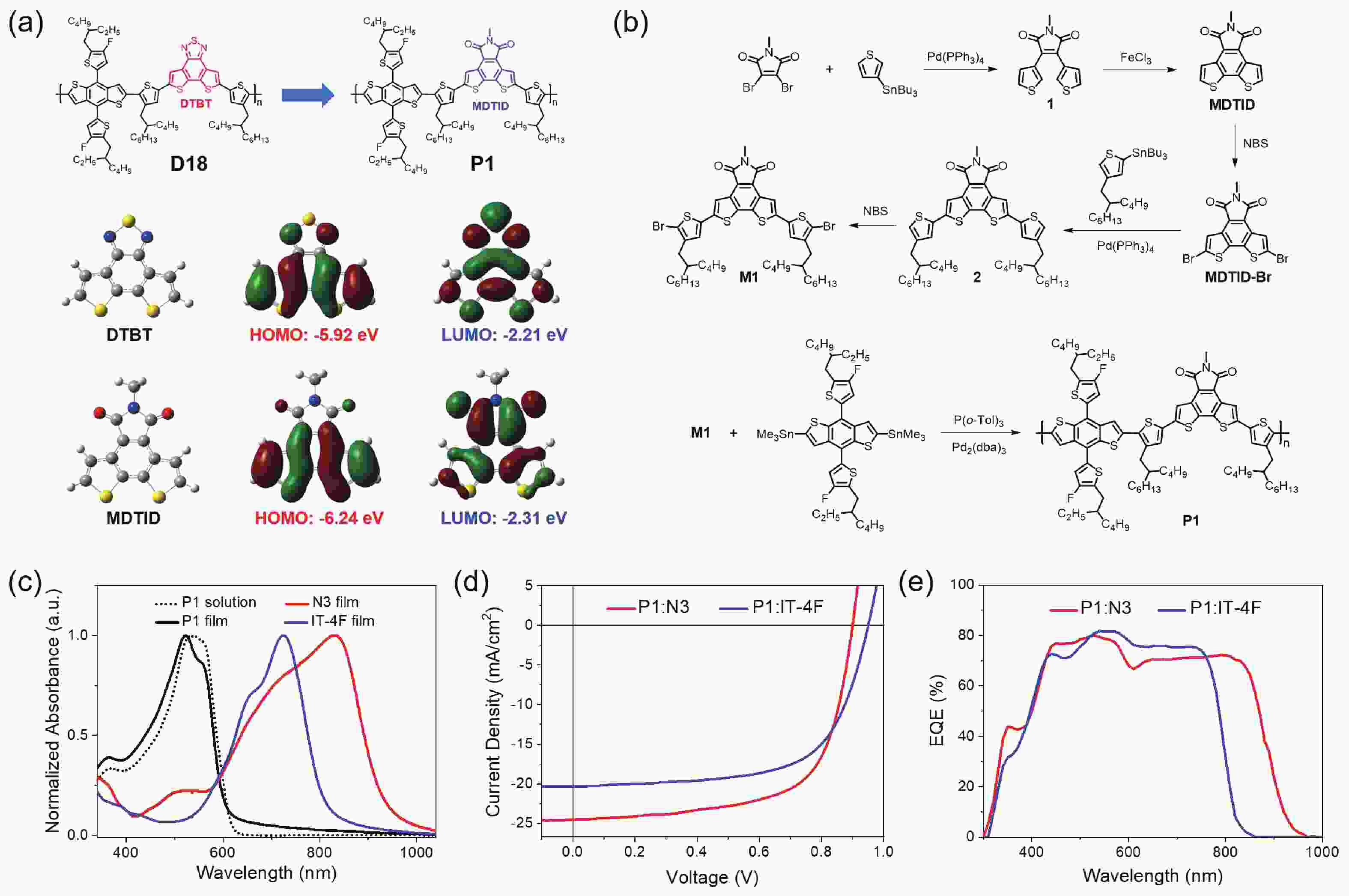
Chemical mechanical polishing (CMP) serves as an indispensable process for achieving global planarization in semiconductor manufacturing, especially as integrated circuit (IC) technology advances to sub-7 nm nodes, where atomic-level surface flatness becomes crucial. Silica abrasives, which account for over 90% of the abrasive market in advanced CMP processes, operate not through simple mechanical grinding but through a key "chemical-mechanical synergistic" mechanism: chemically softening the wafer surface, then mechanically removing the softened layer to expose a new surface, which is further softened and removed, repeating this cycle to produce a smooth wafer. Despite their prevalence, conventional silica abrasives still face challenges, including relatively low material removal rate (MRR), a tendency to agglomerate, leading to poor dispersion and surface defects, and limitations in achieving ultimate surface uniformity. Significant progress has been made to address these issues. Development has progressed from simple spherical particles to complex structural designs (such as mesoporous, hollow, and raspberry-shaped structures) to enhance slurry transport and mechanical action. Surface chemical modifications (e.g., using amino or polymer groups) can improve dispersion stability and reduce scratching. Furthermore, composites with other materials (e.g., ceria, polymers) and precise control of particle size distribution are key to enhancing performance. These innovative approaches have yielded significant performance gains. State-of-the-art slurries have demonstrated the ability to achieve surface roughness below 0.1 nm RMS. The development of silica abrasives is increasingly focused on sustainability and smart manufacturing. A prominent direction is the design of biodegradable abrasives that disintegrate after use, thereby simplifying post-chemical mechanical polishing (CMP) cleanup and minimizing environmental impact—an approach fully aligned with green manufacturing principles. This review systematically summarizes the progress of silica abrasives for CMP over the past 60 years. This summary provides theoretical insights and forward-looking strategies to overcome the current limitations of abrasive technology. We believe this review will be helpful in advancing the field of CMP abrasives towards next-generation semiconductor manufacturing.
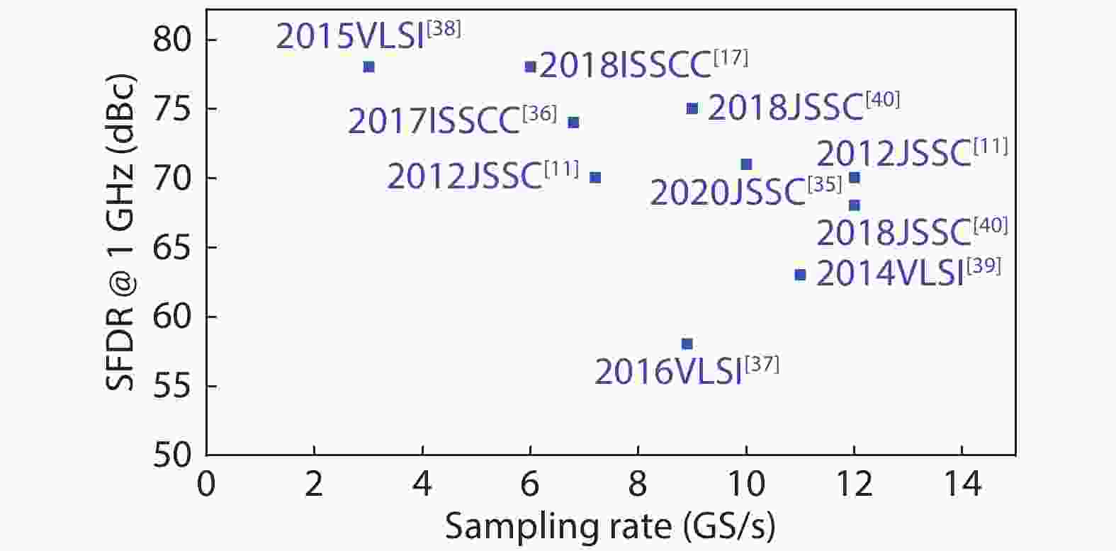
Digital to analog converters (DAC) play an important role as a bridge connecting the analog world and the digital world. With the rapid development of wireless communication, wideband digital radar, and other emerging technologies, better performing high-speed high-resolution DACs are required. In those applications, signal bandwidth and high-frequency linearity often limited by data converters are the bottleneck of the system. This article reviews the state-of-the-art technologies of high-speed and high-resolution DACs reported in recent years. Comparisons are made between different architectures, circuit implementations and calibration techniques along with the figure of merit (FoM) results.

Currently, the global 5G network, cloud computing, and data center industries are experiencing rapid development. The continuous growth of data center traffic has driven the vigorous progress in high-speed optical transceivers for optical interconnection within data centers. The electro-absorption modulated laser (EML), which is widely used in optical fiber communications, data centers, and high-speed data transmission systems, represents a high-performance photoelectric conversion device. Compared to traditional directly modulated lasers (DMLs), EMLs demonstrate lower frequency chirp and higher modulation bandwidth, enabling support for higher data rates and longer transmission distances. This article introduces the composition, working principles, manufacturing processes, and applications of EMLs. It reviews the progress on advanced indium phosphide (InP)-based EML devices from research institutions worldwide, while summarizing and comparing data transmission rates and key technical approaches across various studies.
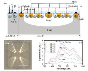
Silicon photonics is an emerging competitive solution for next-generation scalable data communications in different application areas as high-speed data communication is constrained by electrical interconnects. Optical interconnects based on silicon photonics can be used in intra/inter-chip interconnects, board-to-board interconnects, short-reach communications in datacenters, supercomputers and long-haul optical transmissions. In this paper, we present an overview of recent progress in silicon optoelectronic devices and optoelectronic integrated circuits(OEICs) based on a complementary metal-oxide-semiconductor-compatible process, and focus on our research contributions. The silicon optoelectronic devices and OEICs show good characteristics, which are expected to benefit several application domains, including communication, sensing, computing and nonlinear systems.
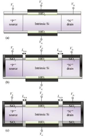
This paper proposes the charge plasma based dual electrode doping-less tunnel FET (DEDLTFET). The paper compares the device performance of the conventional doping-less TFET (DLTFET) and doped TFET (DGTFET). DEDLTEFT gives the superior results with high ON state current (ION ~ 0.56 mA/μm), ION/IOFF ratio ~ 9.12 × 10¹³ and an average subthreshold swing (AV-SS ~ 48 mV/dec). The variation of different device parameters such as channel length, gate oxide material, gate oxide thickness, silicon thickness, gate work function and temperature variation are done and compared with DLTFET and DGTFET. Through the extensive analysis it is found that DEDLTFET shows the better performance than the other two devices, which gives the indication for an excellent future in low power applications.
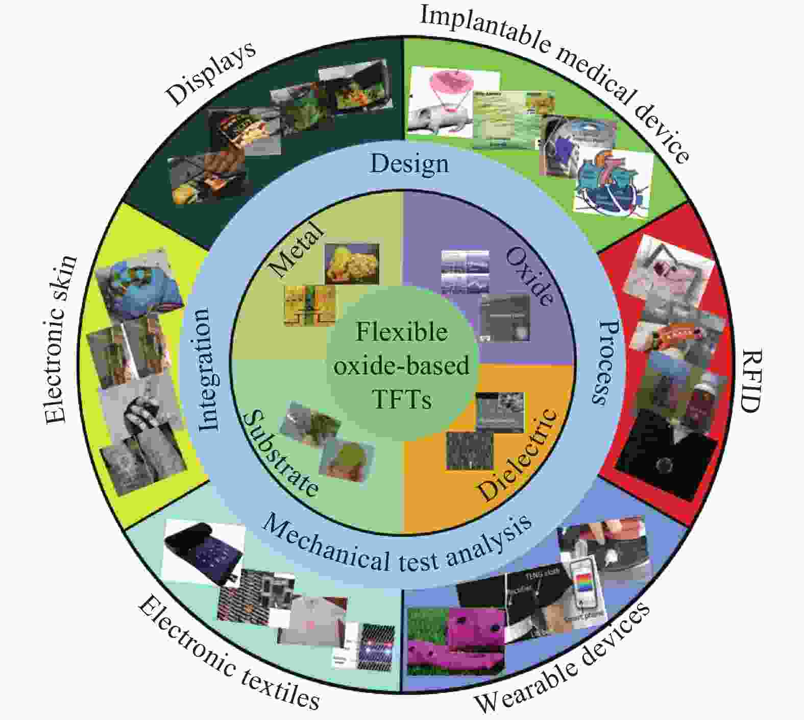
The continuous progress in thin film materials and devices has greatly promoted the development in the field of flexible electronics. As one of the most common thin film devices, thin film transistors (TFTs) are significant building blocks for flexible platforms. Flexible oxide-based TFTs are well compatible with flexible electronic systems due to low process temperature, high carrier mobility, and good uniformity. The present article is a review of the recent progress and major trends in the field of flexible oxide-based thin film transistors. First, an introduction of flexible electronics and flexible oxide-based thin film transistors is given. Next, we introduce oxide semiconductor materials and various flexible oxide-based TFTs classified by substrate materials including polymer plastics, paper sheets, metal foils, and flexible thin glass. Afterwards, applications of flexible oxide-based TFTs including bendable sensors, memories, circuits, and displays are presented. Finally, we give conclusions and a prospect for possible development trends.
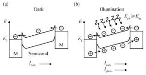
Two-dimensional (2D) materials with unique properties have received a great deal of attention in recent years. This family of materials has rapidly established themselves as intriguing building blocks for versatile nanoelectronic devices that offer promising potential for use in next generation optoelectronics, such as photodetectors. Furthermore, their optoelectronic performance can be adjusted by varying the number of layers. They have demonstrated excellent light absorption, enabling ultrafast and ultrasensitive detection of light in photodetectors, especially in their single-layer structure. Moreover, due to their atomic thickness, outstanding mechanical flexibility, and large breaking strength, these materials have been of great interest for use in flexible devices and strain engineering. Toward that end, several kinds of photodetectors based on 2D materials have been reported. Here, we present a review of the state-of-the-art in photodetectors based on graphene and other 2D materials, such as the graphene, transition metal dichalcogenides, and so on.
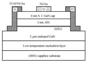
Using the measured capacitance-voltage and current-voltage characteristics of the rectangular AlN/GaN heterostructure field-effect transistors (HFETs) with the side-Ohmic contacts, it was found that the polarization Coulomb field scattering in the AlN/GaN HFETs was greatly weakened after the side-Ohmic contact processing, however, it still could not be ignored. It was also found that, with side-Ohmic contacts, the polarization Coulomb field scattering was much stronger in AlN/GaN HFETs than in AlGaN/AlN/GaN and In0.17Al0.83N/AlN/GaN HFETs, which was attributed to the extremely thinner barrier layer and the stronger polarization of the AlN/GaN heterostructure.


