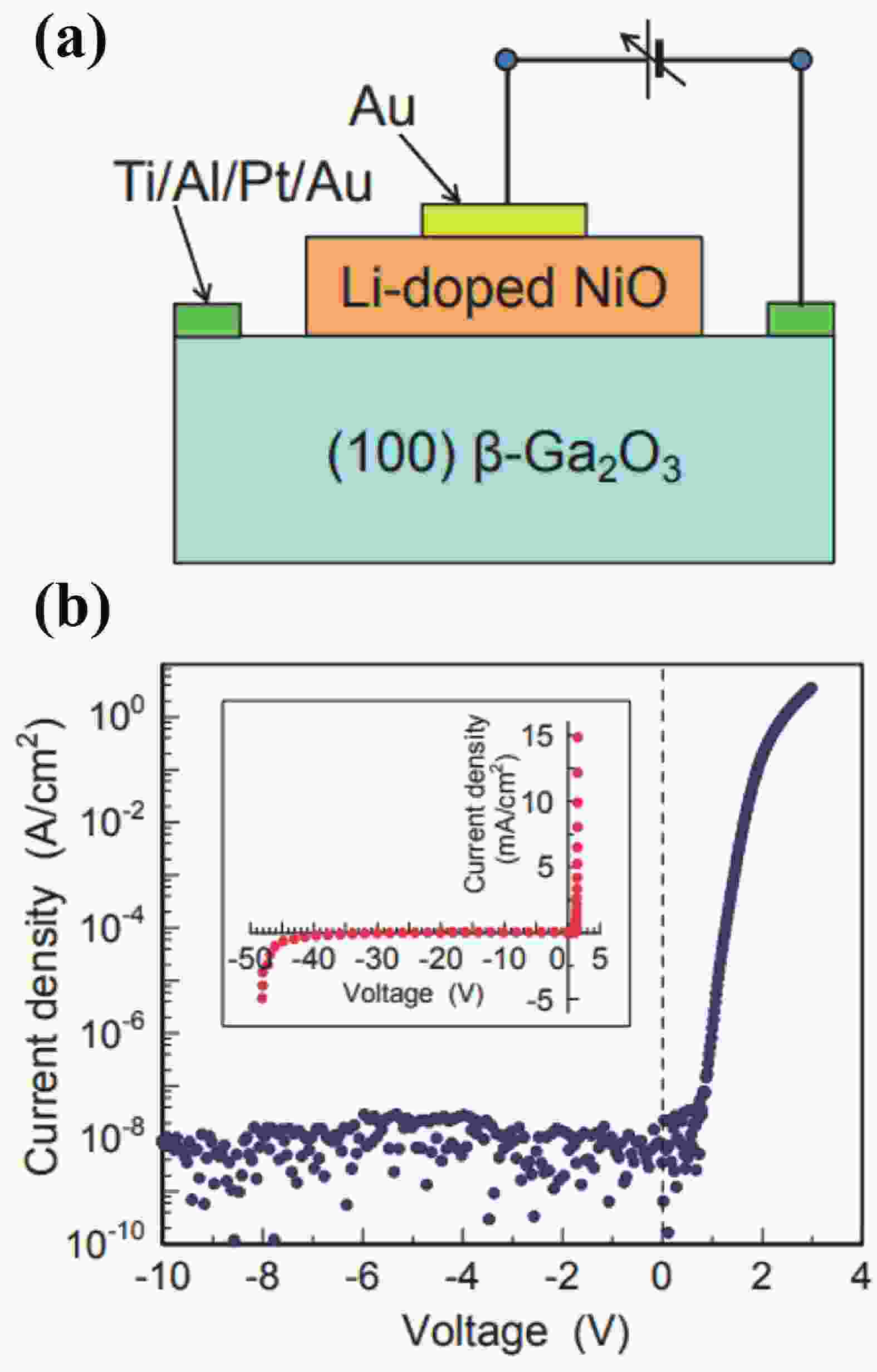
Beta gallium oxide (β-Ga2O3) has attracted significant attention for applications in power electronics due to its ultra-wide bandgap of ~ 4.8 eV and the large critical electric field of 8 MV/cm. These properties yield a high Baliga’s figures of merit (BFOM) of more than 3000. Though β-Ga2O3 possesses superior material properties, the lack of p-type doping is the main obstacle that hinders the development of β-Ga2O3-based power devices for commercial use. Constructing heterojunctions by employing other p-type materials has been proven to be a feasible solution to this issue. Nickel oxide (NiO) is the most promising candidate due to its wide band gap of 3.6–4.0 eV. So far, remarkable progress has been made in NiO/β-Ga2O3 heterojunction power devices. This review aims to summarize recent advances in the construction, characterization, and device performance of the NiO/β-Ga2O3 heterojunction power devices. The crystallinity, band structure, and carrier transport property of the sputtered NiO/β-Ga2O3 heterojunctions are discussed. Various device architectures, including the NiO/β-Ga2O3 heterojunction pn diodes (HJDs), junction barrier Schottky (JBS) diodes, and junction field effect transistors (JFET), as well as the edge terminations and super-junctions based on the NiO/β-Ga2O3 heterojunction, are described.
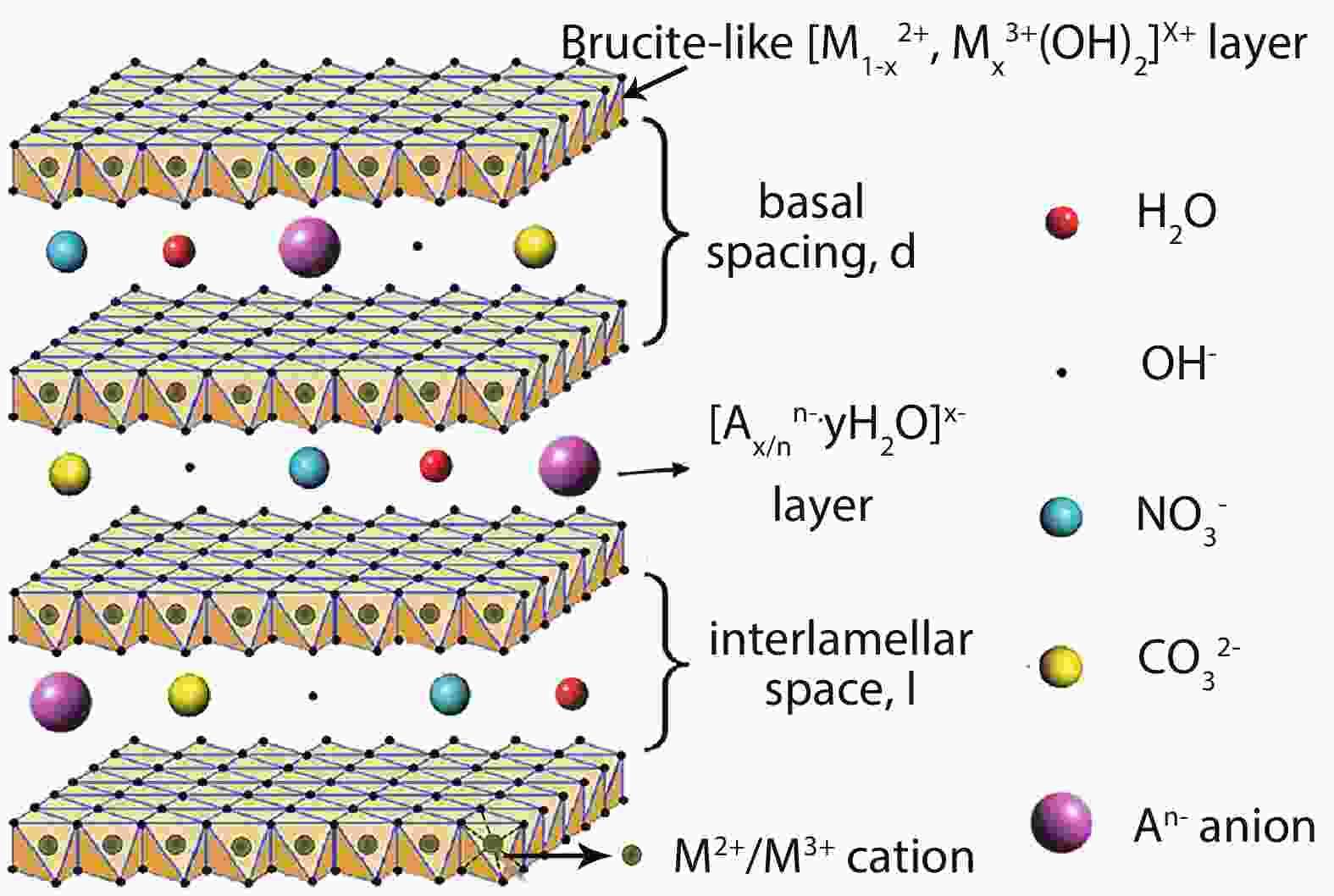
To prevent and mitigate environmental degradation, high-performance and cost-effective electrochemical flexible energy storage systems need to be urgently developed. This demand has led to an increase in research on electrode materials for high-capacity flexible supercapacitors and secondary batteries, which have greatly aided the development of contemporary digital communications and electric vehicles. The use of layered double hydroxides (LDHs) as electrode materials has shown productive results over the last decade, owing to their easy production, versatile composition, low cost, and excellent physicochemical features. This review highlights the distinctive 2D sheet-like structures and electrochemical characteristics of LDH materials, as well as current developments in their fabrication strategies for expanding the application scope of LDHs as electrode materials for flexible supercapacitors and alkali metal (Li, Na, K) ion batteries.

With the rapid technological innovation in materials engineering and device integration, a wide variety of textile-based wearable biosensors have emerged as promising platforms for personalized healthcare, exercise monitoring, and pre-diagnostics. This paper reviews the recent progress in sweat biosensors and sensing systems integrated into textiles for wearable body status monitoring. The mechanisms of biosensors that are commonly adopted for biomarkers analysis are first introduced. The classification, fabrication methods, and applications of textile conductors in different configurations and dimensions are then summarized. Afterward, innovative strategies to achieve efficient sweat collection with textile-based sensing patches are presented, followed by an in-depth discussion on nanoengineering and system integration approaches for the enhancement of sensing performance. Finally, the challenges of textile-based sweat sensing devices associated with the device reusability, washability, stability, and fabrication reproducibility are discussed from the perspective of their practical applications in wearable healthcare.
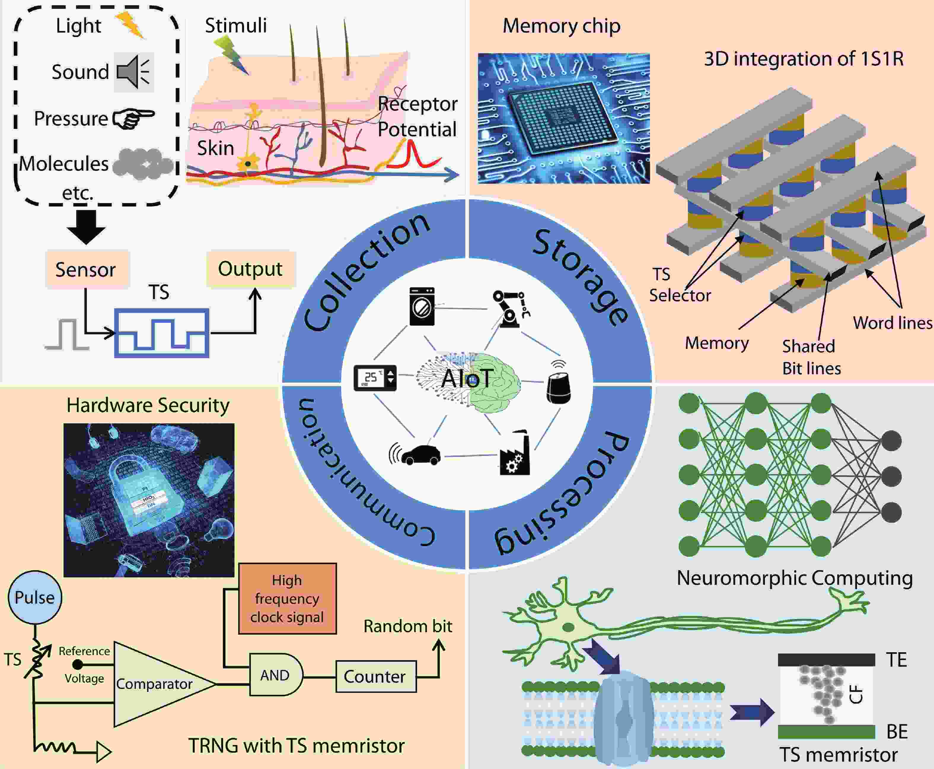
With rapid advancement and deep integration of artificial intelligence and the internet-of-things, artificial intelligence of things has emerged as a promising technology changing people’s daily life. Massive growth of data generated from the devices challenges the AIoT systems from information collection, storage, processing and communication. In the review, we introduce volatile threshold switching memristors, which can be roughly classified into three types: metallic conductive filament-based TS devices, amorphous chalcogenide-based ovonic threshold switching devices, and metal-insulator transition based TS devices. They play important roles in high-density storage, energy efficient computing and hardware security for AIoT systems. Firstly, a brief introduction is exhibited to describe the categories (materials and characteristics) of volatile TS devices. And then, switching mechanisms of the three types of TS devices are discussed and systematically summarized. After that, attention is focused on the applications in 3D cross-point memory technology with high storage-density, efficient neuromorphic computing, hardware security (true random number generators and physical unclonable functions), and others (steep subthreshold slope transistor, logic devices, etc.). Finally, the major challenges and future outlook of volatile threshold switching memristors are presented.
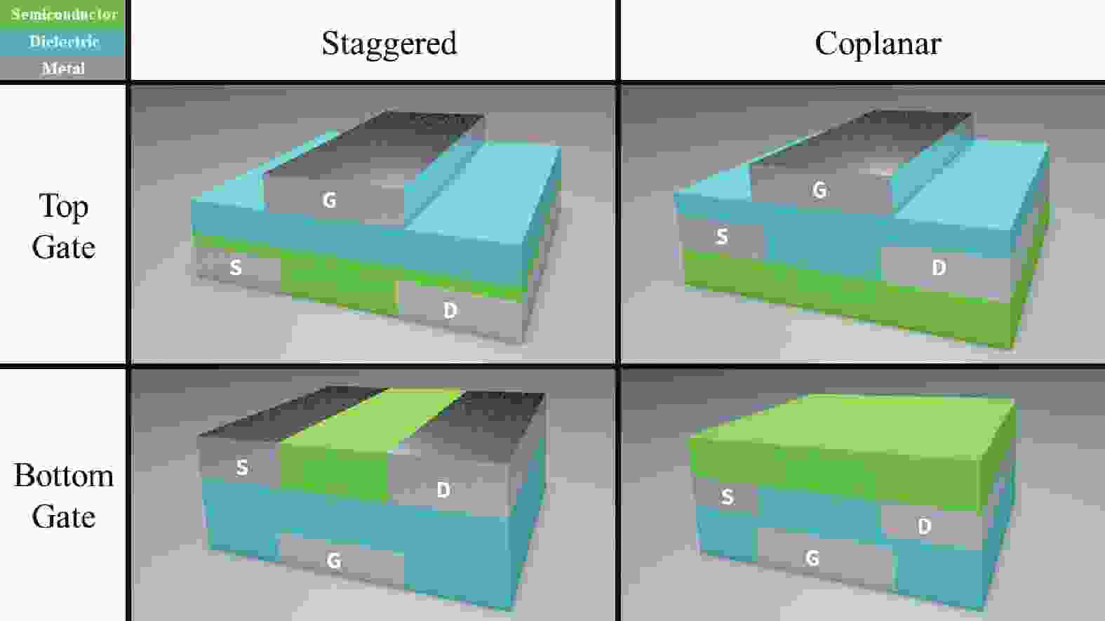
Indium-tin-zinc oxide (ITZO) thin-film transistor (TFT) technology holds promise for achieving high mobility and offers significant opportunities for commercialization. This paper provides a review of progress made in improving the mobility of ITZO TFTs. This paper begins by describing the development and current status of metal-oxide TFTs, and then goes on to explain the advantages of selecting ITZO as the TFT channel layer. The evaluation criteria for TFTs are subsequently introduced, and the reasons and significance of enhancing mobility are clarified. This paper then explores the development of high-mobility ITZO TFTs from five perspectives: active layer optimization, gate dielectric optimization, electrode optimization, interface optimization, and device structure optimization. Finally, a summary and outlook of the research field are presented.
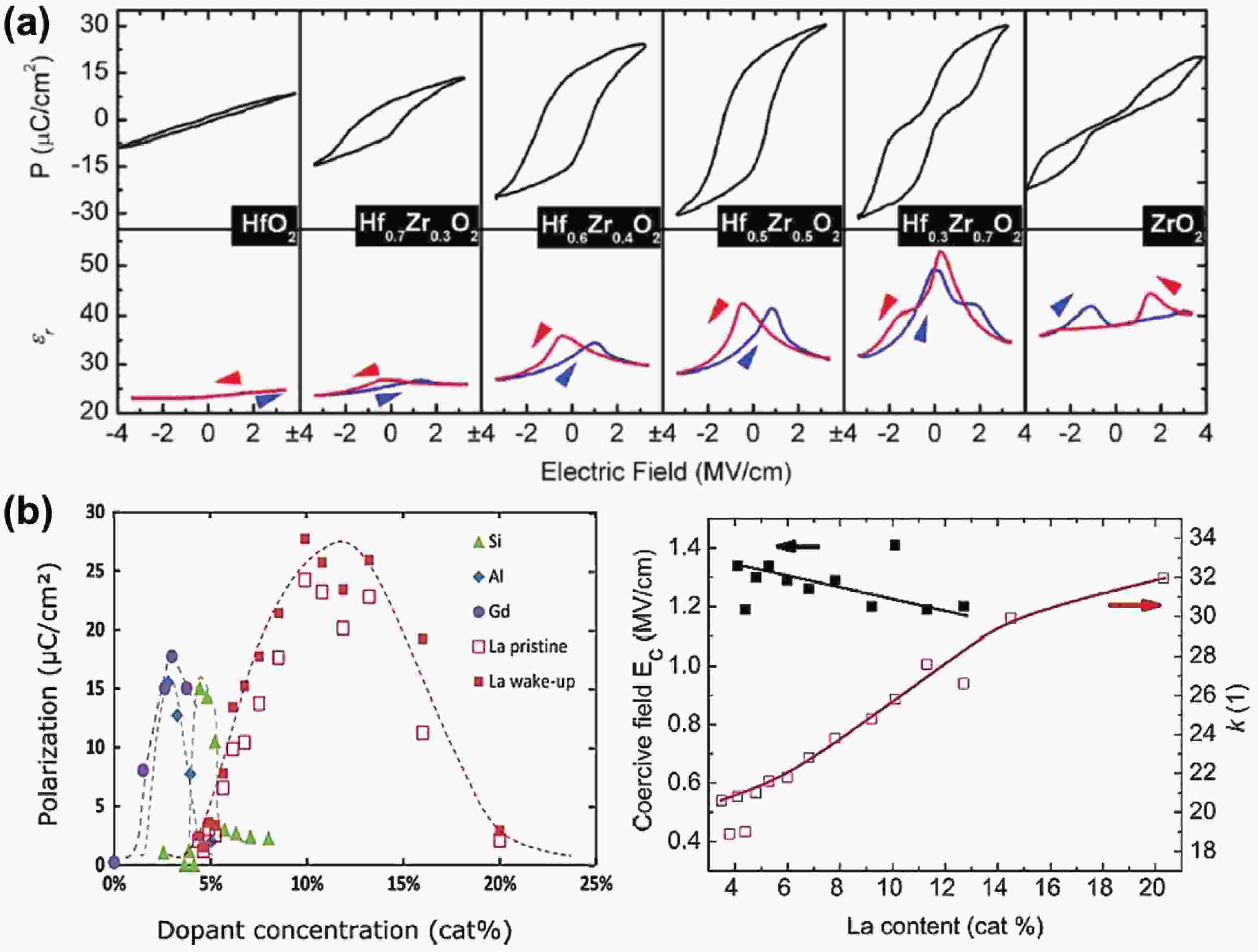
The finding of the robust ferroelectricity in HfO2-based thin films is fantastic from the view point of both the fundamentals and the applications. In this review article, the current research status of the future prospects for the ferroelectric HfO2-based thin films and devices are presented from fundamentals to applications. The related issues are discussed, which include: 1) The ferroelectric characteristics observed in HfO2-based films and devices associated with the factors of dopant, strain, interface, thickness, defect, fabrication condition, and more; 2) physical understanding on the observed ferroelectric behaviors by the density functional theory (DFT)-based theory calculations; 3) the characterizations of microscopic and macroscopic features by transmission electron microscopes-based and electrical properties-based techniques; 4) modeling and simulations, 5) the performance optimizations, and 6) the applications of some ferroelectric-based devices such as ferroelectric random access memory, ferroelectric-based field effect transistors, and the ferroelectric tunnel junction for the novel information processing systems.
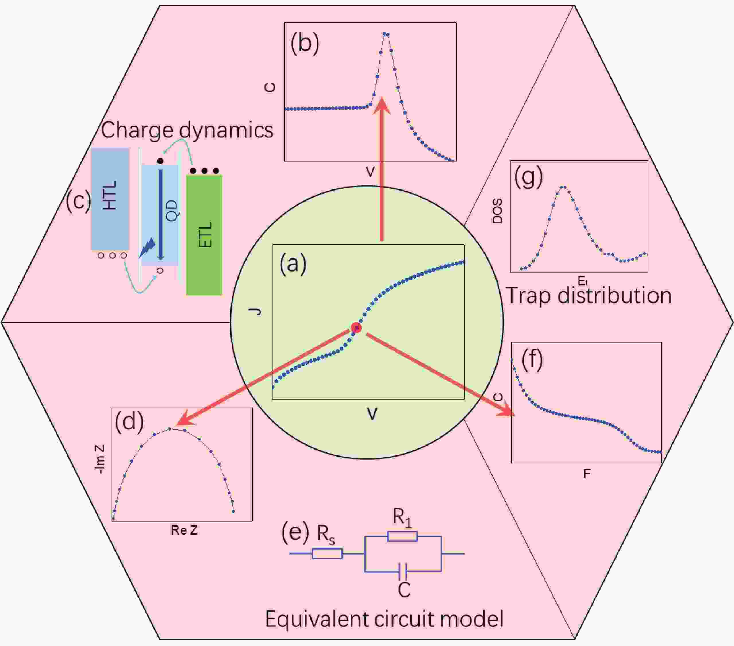
Impedance spectroscopy has been increasingly employed in quantum dot light-emitting diodes (QLEDs) to investigate the charge dynamics and device physics. In this review, we introduce the mathematical basics of impedance spectroscopy that applied to QLEDs. In particular, we focus on the Nyquist plot, Mott−Schottky analysis, capacitance-frequency and capacitance-voltage characteristics, and the dC/dV measurement of the QLEDs. These impedance measurements can provide critical information on electrical parameters such as equivalent circuit models, characteristic time constants, charge injection and recombination points, and trap distribution of the QLEDs. However, this paper will also discuss the disadvantages and limitations of these measurements. Fundamentally, this review provides a deeper understanding of the device physics of QLEDs through the application of impedance spectroscopy, offering valuable insights into the analysis of performance loss and degradation mechanisms of QLEDs.
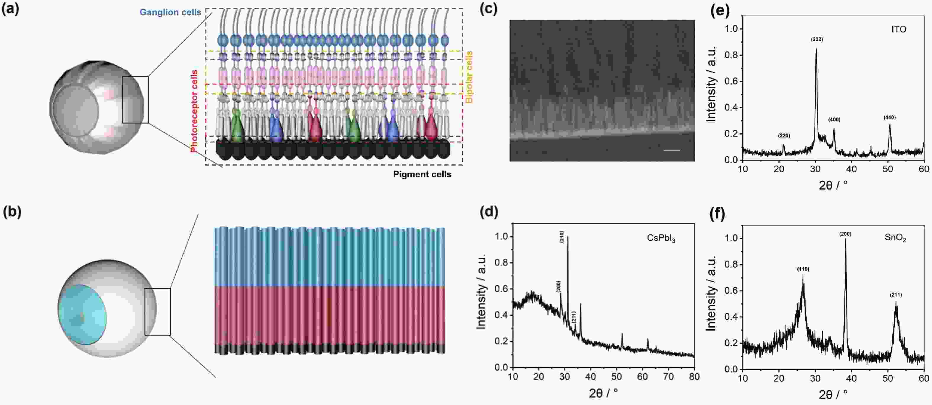
The high-density, vertically aligned retinal neuron array provides effective vision, a feature we aim to replicate with electronic devices. However, the conventional complementary metal-oxide-semiconductor (CMOS) image sensor, based on separate designs for sensing, memory, and processing units, limits its integration density. Moreover, redundant signal communication significantly increases energy consumption. Current neuromorphic devices integrating sensing and signal processing show promise in various computer vision applications, but there is still a need for frame-based imaging with good compatibility. In this study, we developed a dual-mode image sensor based on a high-density all-inorganic perovskite nanowire array. The device can switch between frame-based standard imaging mode and neuromorphic imaging mode by applying different biases. This unique bias-dependent photo response is based on a well-designed energy band diagram. The biomimetic alignment of nanowires ensures the potential for high-resolution imaging. To further demonstrate the imaging ability, we conducted pattern reconstruction in both modes with a 10 × 10 crossbar device. This study introduces a novel image sensor with high compatibility and efficiency, suitable for various applications including computer vision, surveillance, and robotics.
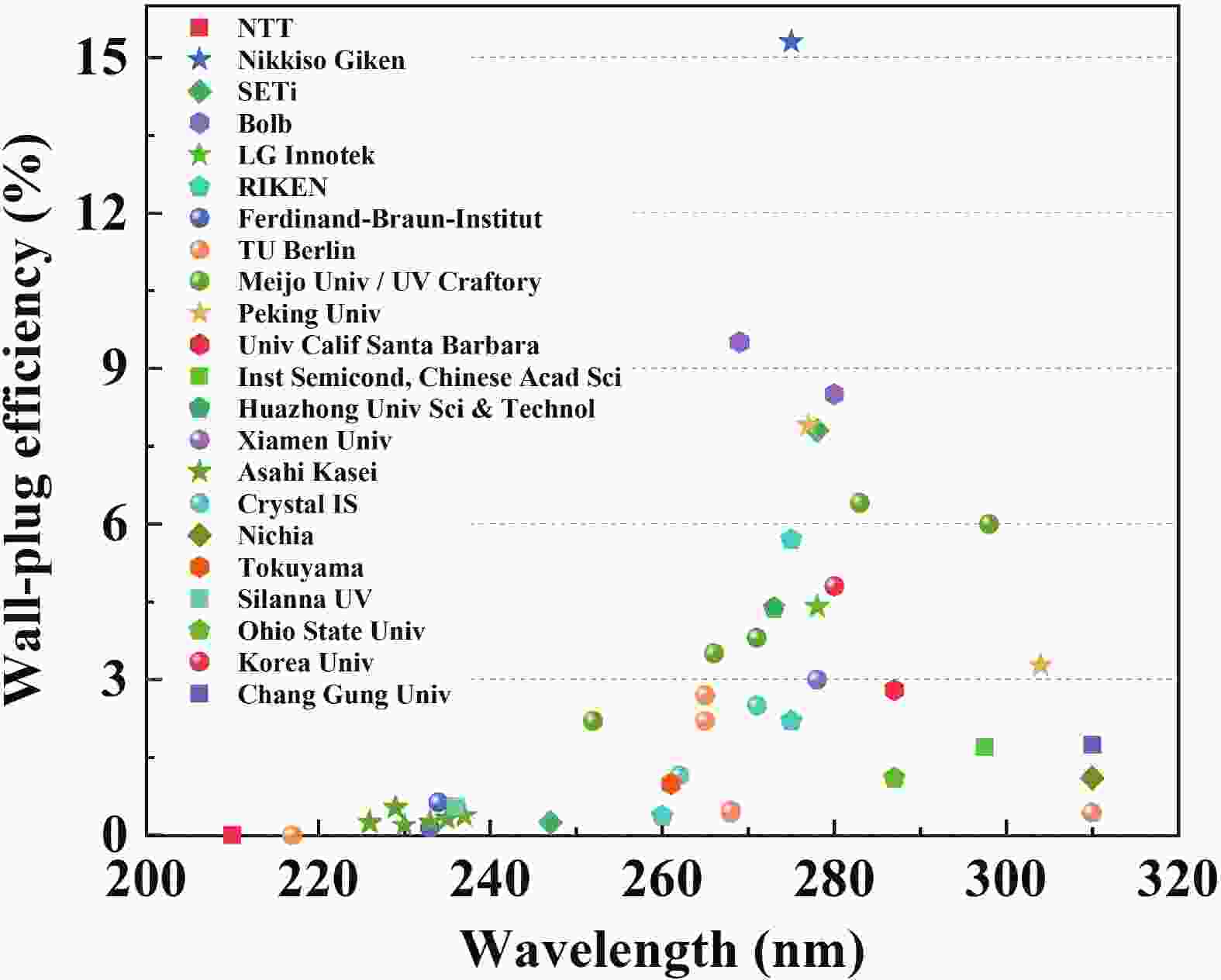
The development of semiconductors is always accompanied by the progress in controllable doping techniques. Taking AlGaN-based ultraviolet (UV) emitters as an example, despite a peak wall-plug efficiency of 15.3% at the wavelength of 275 nm, there is still a huge gap in comparison with GaN-based visible light-emitting diodes (LEDs), mainly attributed to the inefficient doping of AlGaN with increase of the Al composition. First, p-doping of Al-rich AlGaN is a long-standing challenge and the low hole concentration seriously restricts the carrier injection efficiency. Although p-GaN cladding layers are widely adopted as a compromise, the high injection barrier of holes as well as the inevitable loss of light extraction cannot be neglected. While in terms of n-doping the main issue is the degradation of the electrical property when the Al composition exceeds 80%, resulting in a low electrical efficiency in sub-250 nm UV-LEDs. This review summarizes the recent advances and outlines the major challenges in the efficient doping of Al-rich AlGaN, meanwhile the corresponding approaches pursued to overcome the doping issues are discussed in detail.
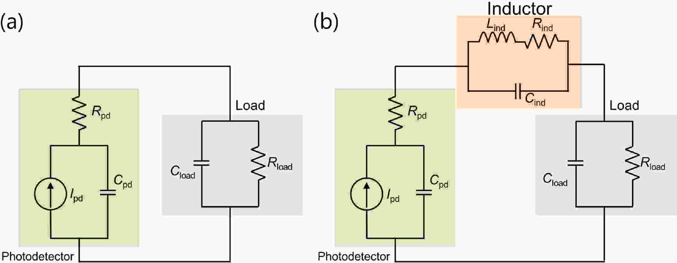
High-performance germanium (Ge) waveguide photodetectors are designed and fabricated utilizing the inductive-gain-peaking technique. With the appropriate integrated inductors, the 3-dB bandwidth of photodetectors is significantly improved owing to the inductive-gain-peaking effect without any compromises to the dark current and optical responsivity. Measured 3-dB bandwidth up to 75 GHz is realized and clear open eye diagrams at 64 Gbps are observed. In this work, the relationship between the frequency response and large signal transmission characteristics on the integrated inductors of Ge waveguide photodetectors is investigated, which indicates the high-speed performance of photodetectors using the inductive-gain-peaking technique.
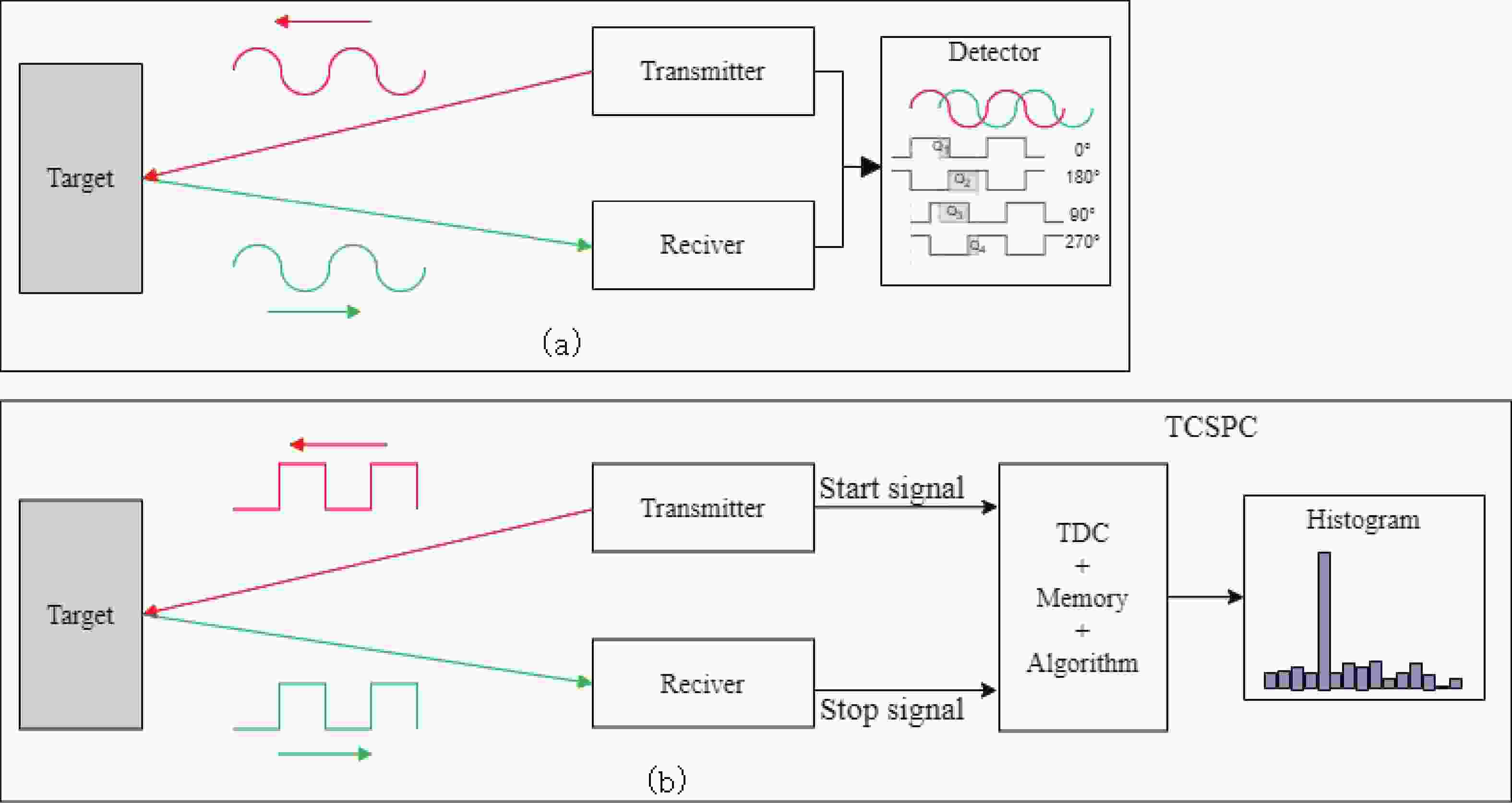
In recent years, propelled by the rapid iterative advancements in digital imaging technology and the semiconductor industry, encompassing microelectronic design, manufacturing, packaging, and testing, time-of-flight (ToF)-based imaging systems for acquiring depth information have garnered considerable attention from both academia and industry. This technology has emerged as a focal point of research within the realm of 3D imaging. Owing to its relatively straightforward principles and exceptional performance, ToF technology finds extensive applications across various domains including human−computer interaction, autonomous driving, industrial inspection, medical and healthcare, augmented reality, smart homes, and 3D reconstruction, among others. Notably, the increasing maturity of ToF-based LiDAR systems is evident in current developments. This paper comprehensively reviews the fundamental principles of ToF technology and LiDAR systems, alongside recent research advancements. It elucidates the innovative aspects and technical challenges encountered in both transmitter (TX) and receiver (RX), providing detailed discussions on corresponding solutions. Furthermore, the paper explores prospective avenues for future research, offering valuable insights for subsequent investigations.
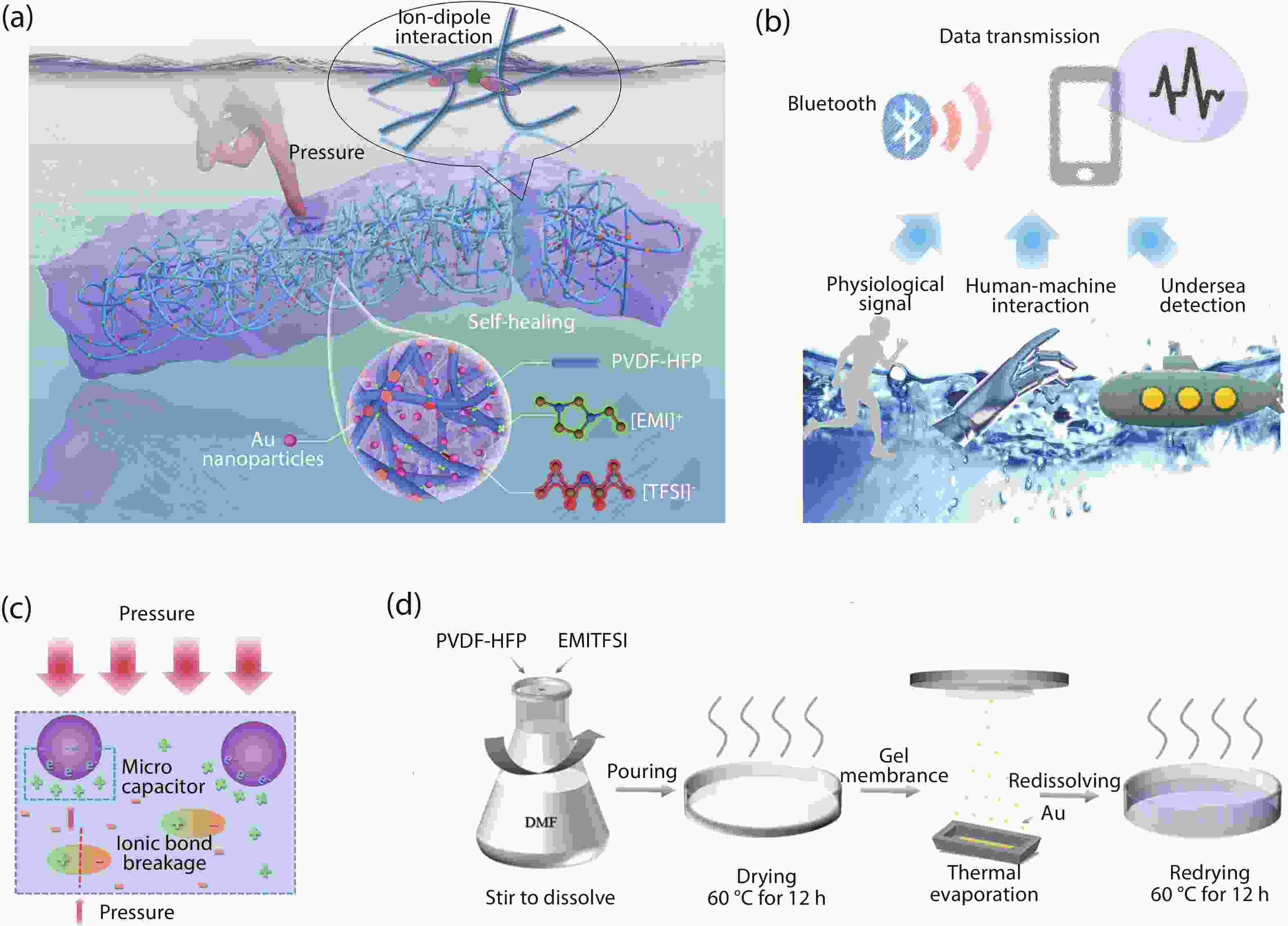
Ionic gels can be potentially used in wearable devices owing to their high humidity resistance and non-volatility. However, the applicability of existing ionic gel pressure sensors is limited by their low sensitivity. Therefore, it is very important to develop an ionic gel pressure sensor with high sensitivity and a wide pressure detection range without sacrificing mechanical stretchability and self-healing ability. Herein, we report an effective strategy for developing pressure sensors based on ionic gel composites consisting of high-molecular-weight polymers, ionic liquids, and Au nanoparticles. The resulting capacitive pressure sensors exhibit high pressure sensitivity, fast response, and excellent self-healing properties. The sensors composed of highly hydrophobic polymers and ionic liquids can be used to track underwater movements, demonstrating broad application prospects in human motion state monitoring and underwater mechanical operations.
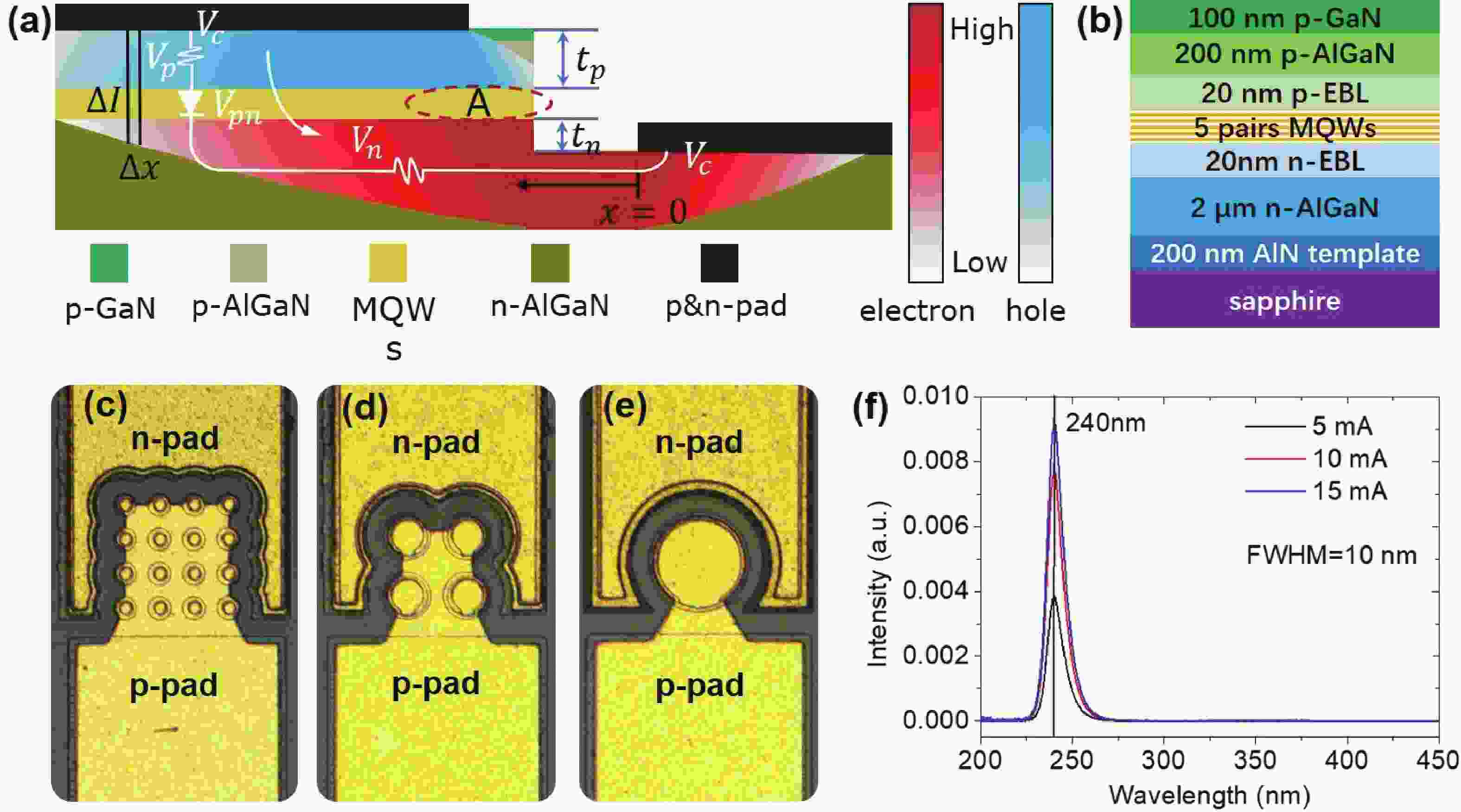
240 nm AlGaN-based micro-LEDs with different sizes are designed and fabricated. Then, the external quantum efficiency (EQE) and light extraction efficiency (LEE) are systematically investigated by comparing size and edge effects. Here, it is revealed that the peak optical output power increases by 81.83% with the size shrinking from 50.0 to 25.0 μm. Thereinto, the LEE increases by 26.21% and the LEE enhancement mainly comes from the sidewall light extraction. Most notably, transverse-magnetic (TM) mode light intensifies faster as the size shrinks due to the tilted mesa side-wall and Al reflector design. However, when it turns to 12.5 μm sized micro-LEDs, the output power is lower than 25.0 μm sized ones. The underlying mechanism is that even though protected by SiO2 passivation, the edge effect which leads to current leakage and Shockley-Read-Hall (SRH) recombination deteriorates rapidly with the size further shrinking. Moreover, the ratio of the p-contact area to mesa area is much lower, which deteriorates the p-type current spreading at the mesa edge. These findings show a role of thumb for the design of high efficiency micro-LEDs with wavelength below 250 nm, which will pave the way for wide applications of deep ultraviolet (DUV) micro-LEDs.
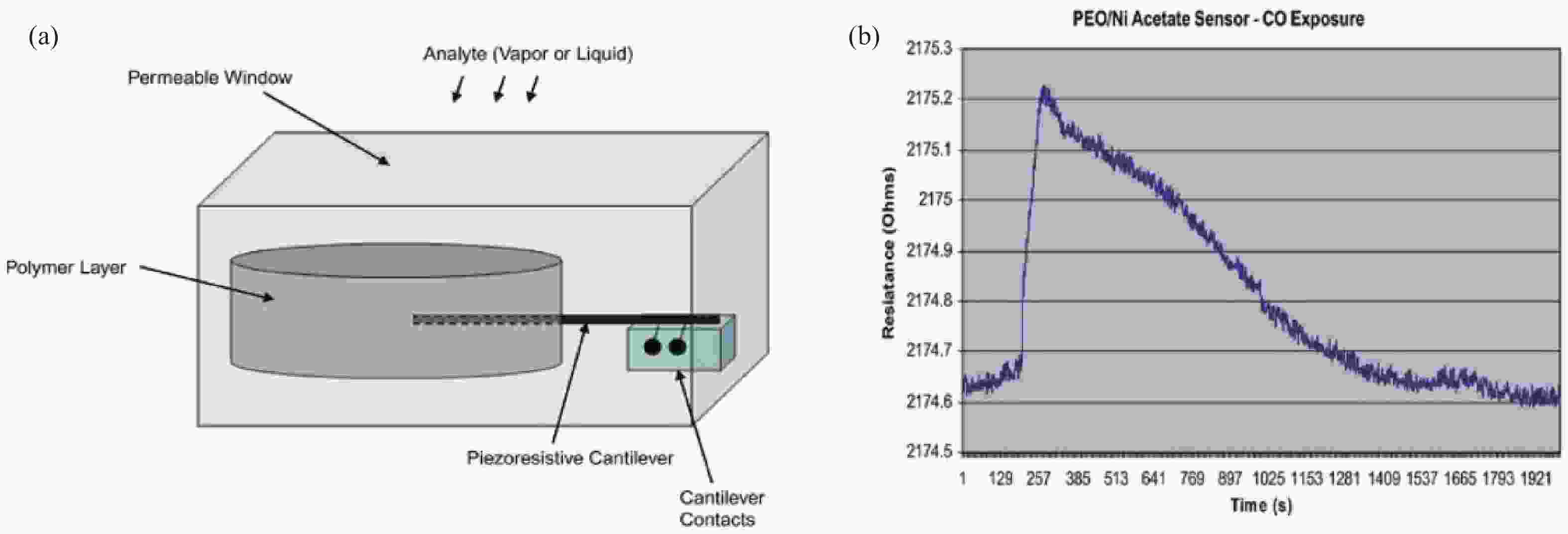
Microcantilever is one of the most popular miniaturized structures in micro-electromechanical systems (MEMS). Sensors based on microcantilever are ideal for biochemical detection, since they have high sensitivity, high throughput, good specification, fast response, thus have attracted extensive attentions. A number of devices that are based on static deflections or shifts of resonant frequency of the cantilevers responding to analyte attachment have been demonstrated. This review comprehensively presents state of art of microcantilever sensors working in gaseous and aqueous environments and highlights the challenges and opportunities of microcantilever biochemical sensors.
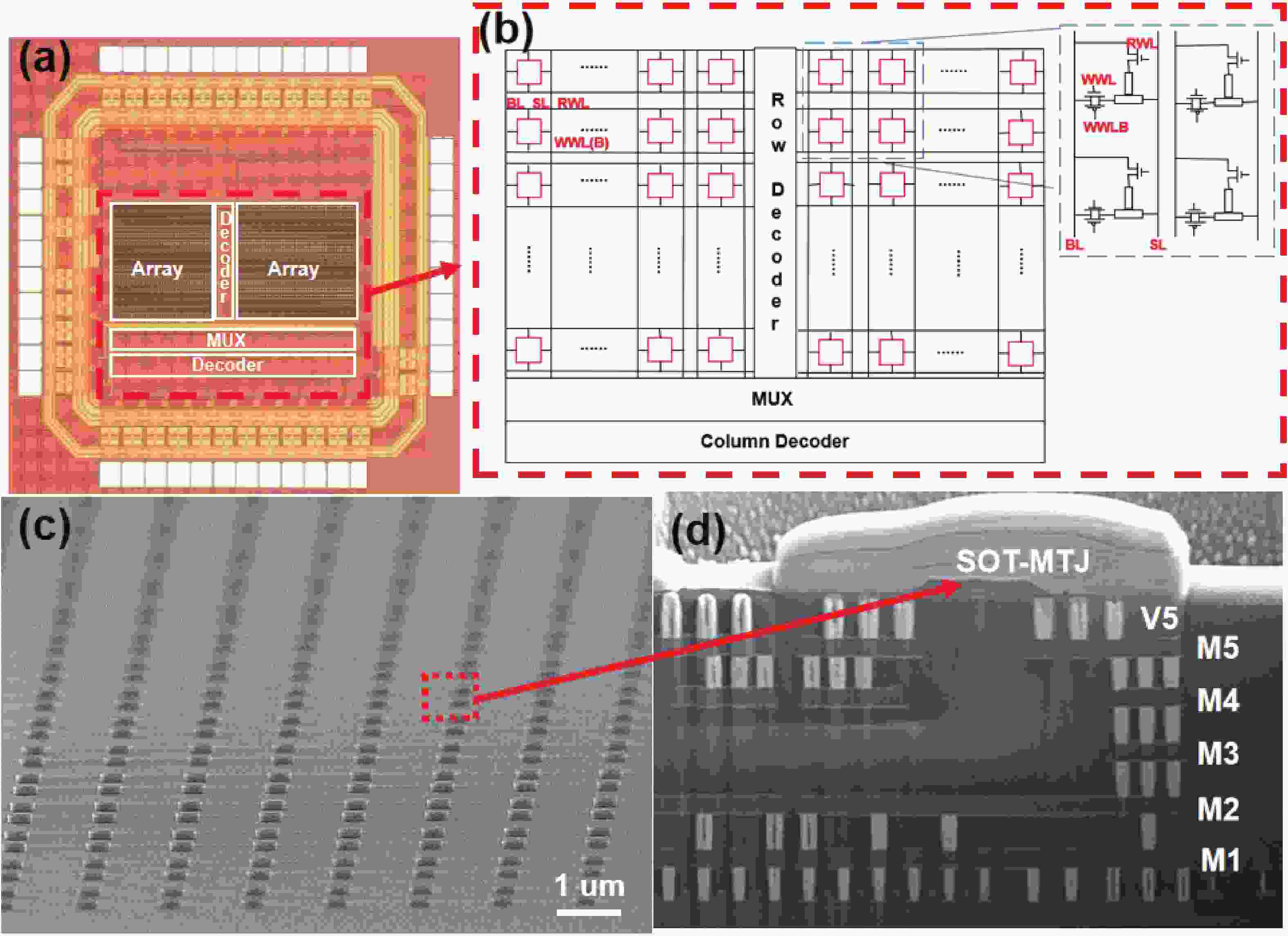
We have successfully demonstrated a 1 Kb spin-orbit torque (SOT) magnetic random-access memory (MRAM) multiplexer (MUX) array with remarkable performance. The 1 Kb MUX array exhibits an in-die function yield of over 99.6%. Additionally, it provides a sufficient readout window, with a TMR/RP_sigma% value of 21.4. Moreover, the SOT magnetic tunnel junctions (MTJs) in the array show write error rates as low as 10−6 without any ballooning effects or back-hopping behaviors, ensuring the write stability and reliability. This array achieves write operations in 20 ns and 1.2 V for an industrial-level temperature range from −40 to 125 °C. Overall, the demonstrated array shows competitive specifications compared to the state-of-the-art works. Our work paves the way for the industrial-scale production of SOT-MRAM, moving this technology beyond R&D and towards widespread adoption.
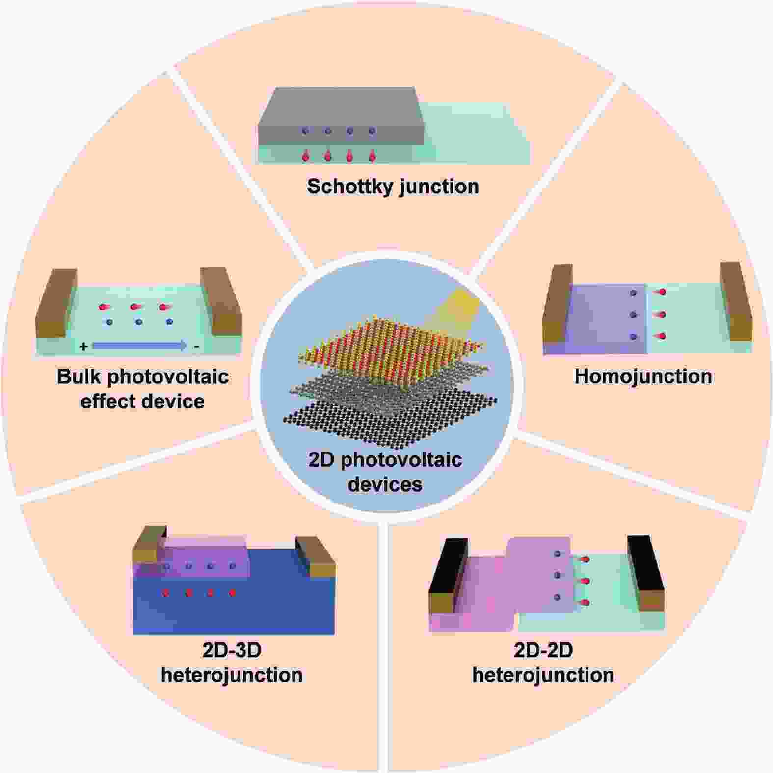
Two-dimensional (2D) materials have attracted tremendous interest in view of the outstanding optoelectronic properties, showing new possibilities for future photovoltaic devices toward high performance, high specific power and flexibility. In recent years, substantial works have focused on 2D photovoltaic devices, and great progress has been achieved. Here, we present the review of recent advances in 2D photovoltaic devices, focusing on 2D-material-based Schottky junctions, homojunctions, 2D−2D heterojunctions, 2D−3D heterojunctions, and bulk photovoltaic effect devices. Furthermore, advanced strategies for improving the photovoltaic performances are demonstrated in detail. Finally, conclusions and outlooks are delivered, providing a guideline for the further development of 2D photovoltaic devices.
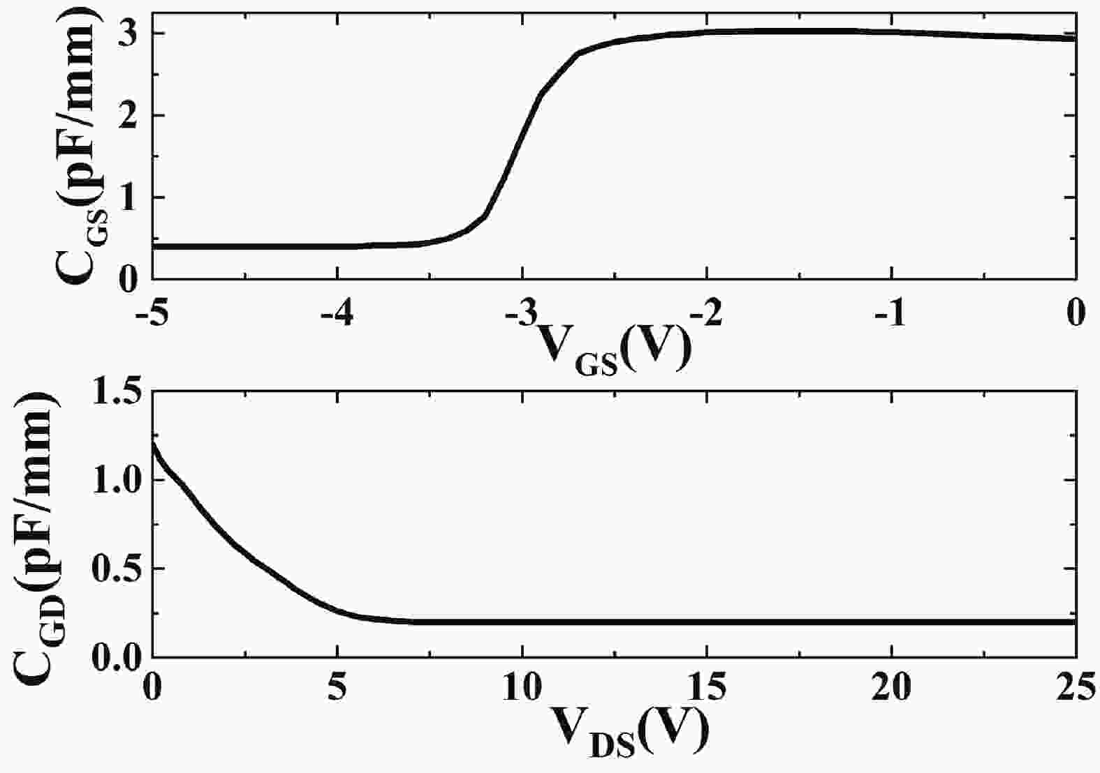
The GaN HEMT is a potential candidate for RF applications due to the high frequency and large power handling capability. To ensure the quality of the communication signal, linearity is a key parameter during the system design. However, the GaN HEMT usually suffers from the nonlinearity problems induced by the nonlinear parasitic capacitance, transconductance, channel transconductance etc. Among them, the transconductance reduction is the main contributor for the nonlinearity and is mostly attributed to the scattering effect, the increasing resistance of access region, the self-heating effect and the trapping effects. Based on the mechanisms, device-level improvement methods of transconductance including the trapping suppression, the nanowire channel, the graded channel, the double channel, the transconductance compensation and the new material structures have been proposed recently. The features of each method are reviewed and compared to provide an overview perspective on the linearity of the GaN HEMT at the device level.

Moiré patterns in physics are interference fringes produced when a periodic template is stacked on another similar one with different displacement and twist angles. The phonon in two-dimensional (2D) material affected by moiré patterns in the lattice shows various novel physical phenomena, such as frequency shift, different linewidth, and mediation to the superconductivity. This review gives a brief overview of phonons in 2D moiré superlattice. First, we introduce the theory of the moiré phonon modes based on a continuum approach using the elastic theory and discuss the effect of the moiré pattern on phonons in 2D materials such as graphene and MoS2. Then, we discuss the electron–phonon coupling (EPC) modulated by moiré patterns, which can be detected by the spectroscopy methods. Furthermore, the phonon-mediated unconventional superconductivity in 2D moiré superlattice is introduced. The theory of phonon-mediated superconductivity in moiré superlattice sets up a general framework, which promises to predict the response of superconductivity to various perturbations, such as disorder, magnetic field, and electric displacement field.


