Processing math: 100%
J. Semicond. > 2014, Volume 35 > Issue 2 > 026004

SEMICONDUCTOR TECHNOLOGY

Effects of rapid thermal annealing on ohmic contact of AlGaN/GaN HEMTs

Yanxu Zhu1, , Weiwei Cao1, Yuyu Fan2, Ye Deng1 and Chen Xu1

+ Author Affiliations

 Corresponding author: Zhu Yanxu, Email:zhuyx@bjut.edu.cn

DOI: 10.1088/1674-4926/35/2/026004

PDF

Abstract: Ohmic contacts with Ti/Al/Ti/Au source and drain electrodes on AlGaN/GaN high electron mobility transistors (HEMTs) were fabricated and subjected to rapid thermal annealing (RTA) in flowing N2. The wafer was divided into 5 parts and three of them were annealed for 30 s at 700, 750, and 800℃, respectively, the others were annealed at 750℃ for 25 and 40 s. Due to the RTA, a change from Schottky contact to Ohmic contact has been obtained between the electrode layer and the AlGaN/GaN heterojunction layer. We have achieved a low specific contact resistance of 7.41×10⁻⁶ Ω·cm2 and contact resistance of 0.54 Ω·mm measured by transmission line mode (TLM), and good surface morphology and edge acuity are also desirable by annealing at 750℃ for 30 s. The experiments also indicate that the performance of ohmic contact is first improved, then it reaches a peak, finally degrading with annealing temperature or annealing time rising.

Key words: AlGaN/GaN HEMTRTAohmic contact

AlGaN/GaN-based high-electron mobility transistors (HEMTs) have remarkable potential and are very attractive for high-power, high-frequency devices[1-5]. This is attributed to the attractive physical features of group Ⅲ nitride semiconductors, such as a wide bandgap, large breakdown field, high thermal coefficient, and favorable two-dimensional electron gas formation at the AlGaN/GaN hetero interface together with a high electron saturation velocity. Along with the development of epitaxial material growth technology, GaN-based HEMTs are growing rapidly. Many experiments have been done to achieve further electrical improvement in these transistors with their robust material properties. Large ohmic contact resistance can lead to a serious deterioration of the peak current availability and reliability. Ohmic contact with low resistance is essential in realizing the full potential of AlGaN/GaN HEMTs. Due to the insulating characteristic of AlGaN, Ohmic contact formation for AlGaN/GaN HEMTs may rely on carrier tunneling across AlGaN.

To obtain a better ohmic contact by selective doping, ion implantation has been developed for the source/drain contacts of AlGaN/GaN HEMTs. The characteristics of ion implanted HEMTs were improved using the optimized annealing temperature of 1150 ℃[6]. As reported in Ref. [7], a method of ohmic area recess etching has been used for a direct contact to AlGaN/GaN heterostructures. It removes AlGaN/GaN epitaxial layers with SiCl4 reactive ion etching (RIE) and a direct sideways contact made by the electrode to the 2DEG around the edges of the active-layer mesas or pads. This is believed to be a more efficient carrier transport mechanism than tunneling through the AlGaN barrier. Recent experiments have shown that an in-situ Si3N4 passivation layer under the metal contact results in lower contact resistance than in the test cases where the passivation layer has been removed or is not deposited at all[8].

In general, multilayer metal structure is the most popular method to achieve a good ohmic contact. So far, it typically has a Ti/Al/blocking layer/Au multilayer scheme, such as Ti/Al/Ti/Au[9] and Ti/Al/Ni/Au. Ti, Ni, Mo, or Pt[10] is often used for the blocking layer, which acts as a barrier layer in the metallization scheme. In this paper, we present a detailed investigation of the effects of rapid thermal annealing on the enhancement of Ti/Al/Ti/Au ohmic performance on AlGaN/GaN epitaxial layers. The experiment is set as in Refs. [9, 11].

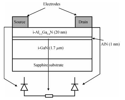
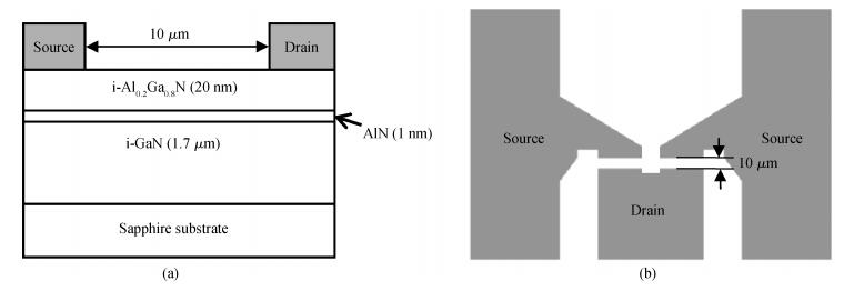
The AlGaN/GaN hetero-junction structure used in this paper is grown by metal-organic chemical vapor deposition (MOCVD) on 150 μm-thick SiC substrates. Both the GaN buffer layer (1.7 μm) and the AlGaN layer (20 nm) are unintentionally doped. A 1 nm AlN layer was inserted between the AlGaN layer and GaN layer; the inserted AlN layer provides a less scattering 2DEG channel and brings a higher mobility or carrier concentration than the samples without the layer[12, 13]. We used conventional photolithography and a lift-off technique to pattern the ohmic contact electrode. Figures 1(a) and 1(b) show the cross-sectional and top view of the fabricated sample, respectively. Fabrication of the diodes started with Ti (15 nm)/Al (150 nm)/Ti (40 nm)/Au (50 nm) ohmic metallization and lifted off. Because we just want to confirm a better annealing condition, the gate electrodes were not sputtered at all. Linear transfer length measurement (TLM) patterns were fabricated for contact performance characterizations on the HEMT layers. The samples were annealed in a rapid thermal annealing system with a series of temperatures and different times, and then electrically measured. The wafer with ohmic contact electrode was divided into 5 parts, three of them were annealed for 30 s at 700, 750 and 800 ℃, respectively. The others were annealed at 750 ℃ for 25 s and 40 s, then compared with the one annealed 30 s at 750 ℃ in the first group of samples.

Figure  1.  (a) Cross sectional and (b) top view of the fabricated sample. The grey regions show ohmic contact electrodes

We measured the I-V curves between the source and drain electrodes. All specific contact resistances (ρc, Ωcm2) and contact resistance (Rc, Ωmm) data are calculated by transmission line model (TLM) method. It is found that the sample with the lowest specific contact resistances (7.41 × 10⁶ Ωcm2) is annealed at 750 ℃ for 30 s. It reaches a lowest contact resistance of 0.54 Ωmm compared to 0.67 Ωmm and 0.98 Ωmm, which were annealed at 700 and 800 for 30 s. On the other hand, the contact resistances of 1.04 Ωmm and 1.2 Ωmm were obtained for samples annealed 25 s and 40 s at 750 ℃, respectively.

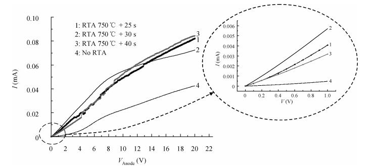
As is shown in Fig. 2, three annealed samples show an ohmic contact compared to the sample without annealing. Before annealing, the sample reveals special back-to-back Schottky diode (Fig. 3.) and shows rectifying properties. The I-V characteristic of the equivalent circuit has the same curve without annealing which is shown in Fig. 2. With annealing at 700 ℃, the contact resistance and series resistance have greatly improved. Therefore a higher temperature should be conducted to improve contact resistance. When the temperature gets to 750 ℃, the ohmic contact characteristics keep improving steadily. But when the temperature is raised to 800 ℃ the performance of the ohmic contact drops down compared to annealing at 750 ℃. When the samples were annealed at 750 ℃ for 30 s, a higher drain current is found compared to the ones without RTA. This indicates that an increased 2DEG concentration ns and a higher mobility μ are achieved after annealing. The curves also show that with the temperature increasing the performance of ohmic contact improved at a low temperature, reached the best ohmic contact, and then finally was degraded at higher temperature. According to the I-V curves, we can also discover that series resistance change a lot after annealing, which means less heat is produced and the reliability of the HEMTs has been improved.

Figure  2.  I-V curves of the samples without annealing in comparison with the ones which were annealed for 700, 750, and 800 ℃, respectively
Figure  3.  Equivalent circuit of the fabricated samples

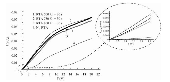
Figure 4 shows the I-V characteristics of annealing at 750 ℃ for 25 s, 30 s, and 40 s, respectively. The samples of annealing for 25 s and 40 s observed an inferior ohmic contact and have bad curves. The group of annealing for 30 s reveals a better performance than the group of annealing for 25 s. The reason is that shorter annealing time leads to the metallization electrodes not completely reacting with the AlGaN/GaN layer. Samples annealed for 40 s show the worst performance. It maybe results from the metal layer turning pelletized with a longer annealing time. Similarly, this can conclude that with the annealing time increasing the ohmic contact resistance become lower first, then get the lowest ohmic resistance, and finally become large again. Considering Figs. 2 and 4, samples annealed at 750 ℃ for 30 s have the best current saturation character compared with other groups.

Figure  4.  I-V curves of the samples with no annealing in comparison with the ones which were annealed at 750 ℃ for 25, 30, and 40 s, respectively

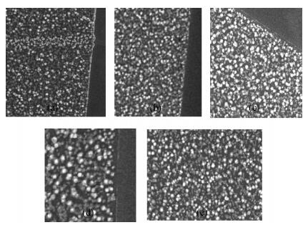
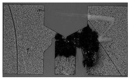
SEM is used to characterize the film smoothness and edge acuity. As shown in Fig. 5, the surface of electrodes gets quite rough and lots of spikes are produced on the surface after annealing at high temperature. According to Fig. 6, some electrodes of the device were burned out when we measured the I-V character at a large current. In conclusion, a rough surface of electrodes is bad for reliability and stability. The roughness is due to the Al existing in the ohmic contact scheme, which does not react completely and is subject to melting at these high annealing temperatures. Because Al plays an essential role in the ohmic contact scheme, another metal cannot be used instead of it or decrease its component. HEMT is usually used as a high-power device and its reliability and stability at large current is important, therefore improving its surface by annealing samples at an optimal condition is very important. Figure 5(a) shows the typical morphology of Ti/Al/Ti/Au electrode annealed at 750 ℃ for 30 s. It is found that a smooth surface and superior edge acuity were obtained in a large area in the sample. There is a continuous increase in metal roughness upon moving from annealing 700 ℃ to 800 ℃. It presents the same trend when the annealing time is increasing. The ohmic contact characteristic presents a similar trend when either annealing temperature or time is increasing. When we considered both of them, we chose the 750 ℃ and 30 s as the annealing condition. Besides, thickening the ohmic contact electrodes when the gate electrodes are fabricated is another way to improve reliability and stability of the device.

Figure  5.  SEM micrographs of different annealing temperature and annealing time. (a) 700 ℃ + RTA 30 s. (b) 750 ℃ + RTA 30 s. (c) 800 ℃ + RTA 30 s. (d) 750 ℃ + RTA 25 s. (e) 750 ℃ + RTA 40 s
Figure  6.  The top view of samples burned out at large current

The contact scheme Ti/Al/Ti/Au is fabricated on AlGaN/GaN heterojunction, which is used for AlGaN/GaN HEMT ohmic contacts. To achieve a change from Schottky contact to ohmic contact, samples were annealed at different temperatures and times. The experiments indicate that, with annealing temperature or annealing time increasing, the performance of the ohmic contact is firstly increased and then decreased. A lower specific contact resistance of 7.41 × 10⁶ Ωcm2 and contact resistance of 0.54 Ωmm, a good surface morphology and edge acuity are achieved when annealing the samples at 750 ℃ for 30 s. There is an approximate range for a lower contact resistance. Therefore, the effects of RTA in Ti/Al/Ti/Au ohmic contact need further studies.


[1]
Wang Jianhui, Wang Xinhua, Pang Lei, et al. Effect of varying layouts on the gate temperature for multi-finger AlGaN/GaN HEMTs. Journal of Semiconductors, 2012, 33(9):094004 doi: 10.1088/1674-4926/33/9/094004
[2]
Shen L, Heikman S, Moran B, et al. AlGaN/AlN/GaN high-power microwave HEMT. IEEE Electron Device Lett, 2001, 22(10):457 doi: 10.1109/55.954910
[3]
Long Fei, Du Jiangfeng, Luo Qian, et al. A research on current collapse of GaN HEMTs under DC high voltage. Chinese Journal of Semiconductors, 2006, 27(z1):227
[4]
Liu Guoguo, Zheng Yingkui, Wei Ke, et al. An 8W X band AlGaN/GaN power HEMT. Journal of Semiconductors, 2008, 29(7):1354 http://www.jos.ac.cn/bdtxben/ch/reader/view_abstract.aspx?file_no=07103001&flag=1
[5]
Shen L, Coffie R, Buttari D, et al. High-power polarization-engineered GaN/AlGaN/GaN HEMTs without surface passivation. IEEE Electron Device Lett, 2004, 25(1):7 doi: 10.1109/LED.2003.821673
[6]
Suita M, Nanjo T, Oishi T, et al. Ion implantation doping for AlGaN/GaN HEMTs. Bremen, Germany:Wiley-VCH Verlag, 2006 doi: 10.1002/pssc.200565135/references
[7]
Wang L, Kim D, Adesida I. Direct contact mechanism of ohmic metallization to AlGaN/GaN heterostructures via ohmic area recess etching. Appl Phys Lett, 2009, 95(17):172107 doi: 10.1063/1.3255014
[8]
Van Daele B, Van Tendeloo G, Derluyn J, et al. Mechanism for ohmic contact formation on Si3N4 passivated AlGaN/GaN high-electron-mobility transistors. Appl Phys Lett, 2006, 89(20):190820 http://cat.inist.fr/?aModele=afficheN&cpsidt=18361176
[9]
Bardwell J A, Haffouz S, Tang H, et al. Electrical characterization and surface morphology of optimized Ti/Al/Ti/Au ohmic contacts for AlGaN/GaN HEMTs. J Electrochem Soc, 2006, 153(8):G746 doi: 10.1149/1.2206998
[10]
Miller M A, Mohney S E. V/Al/V/Ag ohmic contacts to n-AlGaN/GaN heterostructures with a thin GaN cap. Appl Phys Lett, 2007, 91:121031 http://cat.inist.fr/?aModele=afficheN&cpsidt=18970790
[11]
Gong R, Wang J, Dong Z, et al. Analysis on the new mechanisms of low resistance stacked Ti/Al ohmic contact structure on AlGaN/GaN HEMTs. J Phys D:Appl Phys, 2010, 43(39):395102 doi: 10.1088/0022-3727/43/39/395102
[12]
Smorchkova I P, Chen L, Mates T, et al. AlN/GaN and (Al, Ga)N/AlN/GaN two-dimensional electron gas structures grown by plasma-assisted molecular-beam epitaxy. J Appl Phys, 2001, 90(10):5196 doi: 10.1063/1.1412273
[13]
Kaun S W, Wong M H, Mishra U K, et al. Correlation between threading dislocation density and sheet resistance of AlGaN/AlN/GaN heterostructures grown by plasma-assisted molecular beam epitaxy. Appl Phys Lett, 2012, 100(26):210226 doi: 10.1063/1.4730951?journalCode=apl
Fig. 1.  (a) Cross sectional and (b) top view of the fabricated sample. The grey regions show ohmic contact electrodes

Fig. 2.  I-V curves of the samples without annealing in comparison with the ones which were annealed for 700, 750, and 800 ℃, respectively

Fig. 3.  Equivalent circuit of the fabricated samples

Fig. 4.  I-V curves of the samples with no annealing in comparison with the ones which were annealed at 750 ℃ for 25, 30, and 40 s, respectively

Fig. 5.  SEM micrographs of different annealing temperature and annealing time. (a) 700 ℃ + RTA 30 s. (b) 750 ℃ + RTA 30 s. (c) 800 ℃ + RTA 30 s. (d) 750 ℃ + RTA 25 s. (e) 750 ℃ + RTA 40 s

Fig. 6.  The top view of samples burned out at large current

[1]
Wang Jianhui, Wang Xinhua, Pang Lei, et al. Effect of varying layouts on the gate temperature for multi-finger AlGaN/GaN HEMTs. Journal of Semiconductors, 2012, 33(9):094004 doi: 10.1088/1674-4926/33/9/094004
[2]
Shen L, Heikman S, Moran B, et al. AlGaN/AlN/GaN high-power microwave HEMT. IEEE Electron Device Lett, 2001, 22(10):457 doi: 10.1109/55.954910
[3]
Long Fei, Du Jiangfeng, Luo Qian, et al. A research on current collapse of GaN HEMTs under DC high voltage. Chinese Journal of Semiconductors, 2006, 27(z1):227
[4]
Liu Guoguo, Zheng Yingkui, Wei Ke, et al. An 8W X band AlGaN/GaN power HEMT. Journal of Semiconductors, 2008, 29(7):1354 http://www.jos.ac.cn/bdtxben/ch/reader/view_abstract.aspx?file_no=07103001&flag=1
[5]
Shen L, Coffie R, Buttari D, et al. High-power polarization-engineered GaN/AlGaN/GaN HEMTs without surface passivation. IEEE Electron Device Lett, 2004, 25(1):7 doi: 10.1109/LED.2003.821673
[6]
Suita M, Nanjo T, Oishi T, et al. Ion implantation doping for AlGaN/GaN HEMTs. Bremen, Germany:Wiley-VCH Verlag, 2006 doi: 10.1002/pssc.200565135/references
[7]
Wang L, Kim D, Adesida I. Direct contact mechanism of ohmic metallization to AlGaN/GaN heterostructures via ohmic area recess etching. Appl Phys Lett, 2009, 95(17):172107 doi: 10.1063/1.3255014
[8]
Van Daele B, Van Tendeloo G, Derluyn J, et al. Mechanism for ohmic contact formation on Si3N4 passivated AlGaN/GaN high-electron-mobility transistors. Appl Phys Lett, 2006, 89(20):190820 http://cat.inist.fr/?aModele=afficheN&cpsidt=18361176
[9]
Bardwell J A, Haffouz S, Tang H, et al. Electrical characterization and surface morphology of optimized Ti/Al/Ti/Au ohmic contacts for AlGaN/GaN HEMTs. J Electrochem Soc, 2006, 153(8):G746 doi: 10.1149/1.2206998
[10]
Miller M A, Mohney S E. V/Al/V/Ag ohmic contacts to n-AlGaN/GaN heterostructures with a thin GaN cap. Appl Phys Lett, 2007, 91:121031 http://cat.inist.fr/?aModele=afficheN&cpsidt=18970790
[11]
Gong R, Wang J, Dong Z, et al. Analysis on the new mechanisms of low resistance stacked Ti/Al ohmic contact structure on AlGaN/GaN HEMTs. J Phys D:Appl Phys, 2010, 43(39):395102 doi: 10.1088/0022-3727/43/39/395102
[12]
Smorchkova I P, Chen L, Mates T, et al. AlN/GaN and (Al, Ga)N/AlN/GaN two-dimensional electron gas structures grown by plasma-assisted molecular-beam epitaxy. J Appl Phys, 2001, 90(10):5196 doi: 10.1063/1.1412273
[13]
Kaun S W, Wong M H, Mishra U K, et al. Correlation between threading dislocation density and sheet resistance of AlGaN/AlN/GaN heterostructures grown by plasma-assisted molecular beam epitaxy. Appl Phys Lett, 2012, 100(26):210226 doi: 10.1063/1.4730951?journalCode=apl
1

Low ohmic contact AlN/GaN HEMTs grown by MOCVD

Guodong Gu, Shaobo Dun, Yuanjie Lü, Tingting Han, Peng Xu, et al.

Journal of Semiconductors, 2013, 34(11): 114004. doi: 10.1088/1674-4926/34/11/114004

2

Analysis of the ohmic contacts of Ti/Al/Ni/Au to AlGaN/GaN HEMTs by the multi-step annealing process

Yan Wei, Zhang Renping, Du Yandong, Han Weihua, Yang Fuhua, et al.

Journal of Semiconductors, 2012, 33(6): 064005. doi: 10.1088/1674-4926/33/6/064005

3

An 8 GHz high power AlGaN/GaN HEMT VCO

Chen Huifang, Wang Xiantai, Chen Xiaojuan, Luo Weijun, Liu Xinyu, et al.

Journal of Semiconductors, 2010, 31(7): 074012. doi: 10.1088/1674-4926/31/7/074012

4

Gate-structure optimization for high frequency power AlGaN/GaN HEMTs

Wang Dongfang, Yuan Tingting, Wei Ke, Chen Xiaojuan, Liu Xinyu, et al.

Journal of Semiconductors, 2010, 31(5): 054003. doi: 10.1088/1674-4926/31/5/054003

5

High performance AlGaN/GaN HEMTs with 2.4 μm source–drain spacing

Wang Dongfang, Wei Ke, Yuan Tingting, Liu Xinyu

Journal of Semiconductors, 2010, 31(3): 034001. doi: 10.1088/1674-4926/31/3/034001

6

Multi-bias capacitance voltage characteristic of AlGaN/GaN HEMT

Pu Yan, Wang Liang, Yuan Tingting, Ouyang Sihua, Liu Guoguo, et al.

Journal of Semiconductors, 2010, 31(10): 104002. doi: 10.1088/1674-4926/31/10/104002

7

NiO removal of Ni/Au Ohmic contact to p-GaN after annealing

Lin Mengzhe, CaoQing, YanTingjing, ZhangShuming, ChenLianghui, et al.

Journal of Semiconductors, 2009, 30(2): 026001. doi: 10.1088/1674-4926/30/2/026001

8

Impact of UV/ozone surface treatment on AlGaN/GaN HEMTs

Yuan Tingting, Liu Xinyu, Zheng Yingkui, Li Chengzhan, Wei Ke, et al.

Journal of Semiconductors, 2009, 30(12): 124001. doi: 10.1088/1674-4926/30/12/124001

9

Improvements to the extraction of an AlGaN/GaN HEMT small-signal model

Pu Yan, Pang Lei, Wang Liang, Chen Xiaojuan, Li Chengzhan, et al.

Journal of Semiconductors, 2009, 30(12): 124003. doi: 10.1088/1674-4926/30/12/124003

10

Ohmic Contact Property of Ti/Al/Ni/Au on AlGaN/GaN Heterostructures for Application in Ultraviolet Detectors

Zhang Junqin, Yang Yintang, Chai Changchun, Li Yuejin, Jia Hujun, et al.

Journal of Semiconductors, 2008, 29(11): 2187-2191.

11

Carbon-Induced Deep Traps Responsible for Current Collapse in AlGaN/GaN HEMTs

Pang Lei, Li Chengzhan, Wang Dongdong, Huang Jun, Zeng Xuan, et al.

Journal of Semiconductors, 2008, 29(6): 1066-1069.

12

Ohmic Contact Properties of Multi-Metal Films on n-Type 4H-SiC

Han Ru, Yang Yintang, Wang Ping, Cui Zhandong, Li Liang, et al.

Chinese Journal of Semiconductors , 2007, 28(2): 149-153.

13

A Recessed AlGaN/GaN HEMT with High Output Power in the X Band

Feng Zhen, Zhang Zhiguo, Wang Yong, Mo Jianghui, Song Jianbo, et al.

Chinese Journal of Semiconductors , 2007, 28(11): 1773-1776.

14

AlGaN/GaN HEMTs Power Amplifier MIC with Power Combining at C-Band

Yao Xiaojiang, Li Bin, Chen Yanhu, Chen Xiaojuan, Wei Ke, et al.

Chinese Journal of Semiconductors , 2007, 28(4): 514-517.

15

Ohmic Contact to an AlGaN/GaN Heterostructure

Yang Yan, Wang Wenbo, Hao Yue

Chinese Journal of Semiconductors , 2006, 27(10): 1823-1827.

16

Two-Dimensional Static Numerical Modeling and Simulation of AlGaN/GaN HEMT

Xue Lijun, Xia Yang, Liu Ming, Wang Yan, Shao Xue, et al.

Chinese Journal of Semiconductors , 2006, 27(2): 298-303.

17

Effect of Rapid Thermal Annealing Ambient on Denuded Zone and Oxygen Precipitates in a 300mm Silicon Wafer

Feng Quanlin, Shi Xunda, Liu Bin, Liu Zuoxing, Wang Jing, et al.

Chinese Journal of Semiconductors , 2006, 27(1): 68-72.

18

Numerical Explanation of Slow Transients in an AlGaN/GaN HEMT

Zhang Jinfeng, Hao Yue

Chinese Journal of Semiconductors , 2006, 27(2): 276-282.

19

Development of High Performance AlGaN/GaN HEMTswith Low Ohmic Contact

Liu Jian, Li Chenzhan, Wei Ke, He Zhijing, Liu Guoguo, et al.

Chinese Journal of Semiconductors , 2006, 27(S1): 262-265.

20

A New AlGaN/GaN HEMT Semiempirical DC Model

Liu Dan, Chen Xiaojuan, Liu Guoguo, He Zhijing, Liu Xinyu, et al.

Chinese Journal of Semiconductors , 2006, 27(11): 1984-1988.

  • Search

    Advanced Search >>

    GET CITATION

    Yanxu Zhu, Weiwei Cao, Yuyu Fan, Ye Deng, Chen Xu. Effects of rapid thermal annealing on ohmic contact of AlGaN/GaN HEMTs[J]. Journal of Semiconductors, 2014, 35(2): 026004. doi: 10.1088/1674-4926/35/2/026004
    Y X Zhu, W W Cao, Y Y Fan, Y Deng, C Xu. Effects of rapid thermal annealing on ohmic contact of AlGaN/GaN HEMTs[J]. J. Semicond., 2014, 35(2): 026004. doi: 10.1088/1674-4926/35/2/026004.
    shu

    Export: BibTex EndNote

    Article Metrics

    Article views: 4067 Times PDF downloads: 98 Times Cited by: 0 Times

    History

    Received: 04 July 2013 Revised: 11 September 2013 Online: Published: 01 February 2014

    Catalog

      Email This Article

      User name:
      Email:*请输入正确邮箱
      Code:*验证码错误
      Yanxu Zhu, Weiwei Cao, Yuyu Fan, Ye Deng, Chen Xu. Effects of rapid thermal annealing on ohmic contact of AlGaN/GaN HEMTs[J]. Journal of Semiconductors, 2014, 35(2): 026004. doi: 10.1088/1674-4926/35/2/026004 ****Y X Zhu, W W Cao, Y Y Fan, Y Deng, C Xu. Effects of rapid thermal annealing on ohmic contact of AlGaN/GaN HEMTs[J]. J. Semicond., 2014, 35(2): 026004. doi: 10.1088/1674-4926/35/2/026004.
      Citation:
      Yanxu Zhu, Weiwei Cao, Yuyu Fan, Ye Deng, Chen Xu. Effects of rapid thermal annealing on ohmic contact of AlGaN/GaN HEMTs[J]. Journal of Semiconductors, 2014, 35(2): 026004. doi: 10.1088/1674-4926/35/2/026004 ****
      Y X Zhu, W W Cao, Y Y Fan, Y Deng, C Xu. Effects of rapid thermal annealing on ohmic contact of AlGaN/GaN HEMTs[J]. J. Semicond., 2014, 35(2): 026004. doi: 10.1088/1674-4926/35/2/026004.

      Effects of rapid thermal annealing on ohmic contact of AlGaN/GaN HEMTs

      DOI: 10.1088/1674-4926/35/2/026004
      Funds:

      the National Natural Science Foundation of China 61107026

      Project supported by the National Natural Science Foundation of China (No. 61107026) and the Scientific Research Fund Project of Municipal Education Commission of Beijing (No. KM201210005004)

      the Scientific Research Fund Project of Municipal Education Commission of Beijing KM201210005004

      More Information
      • Corresponding author: Zhu Yanxu, Email:zhuyx@bjut.edu.cn
      • Received Date: 2013-07-04
      • Revised Date: 2013-09-11
      • Published Date: 2014-02-01

      Catalog

        /

        DownLoad:  Full-Size Img  PowerPoint
        Return
        Return