Fig. 1.
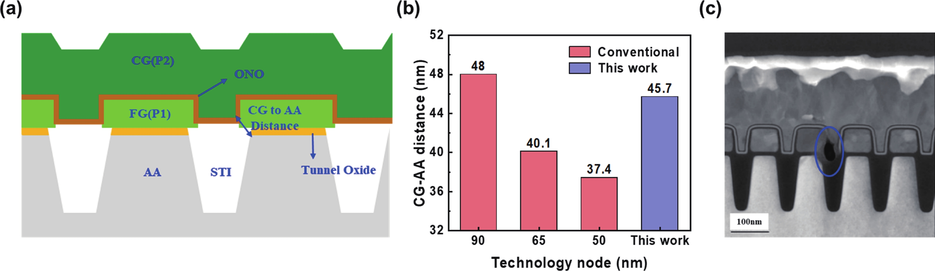
(Color online) (a) A schematic of NOR flash cell structure. (b) The trend between scaling down node and CG-AA distance. (c) Cross section TEM image of CG-AA burnout issue.
ARTICLES
Kevin Fang1, 2, Wei Wang2, Yibai Xue1, Fan Wang2, Dong Pan2, Yi Li1, and Jerry Zhou1, 2,
Corresponding author: Yi Li, liyi@hust.edu.cn; Jerry Zhou, Jerry_Zhou@xmcwh.com
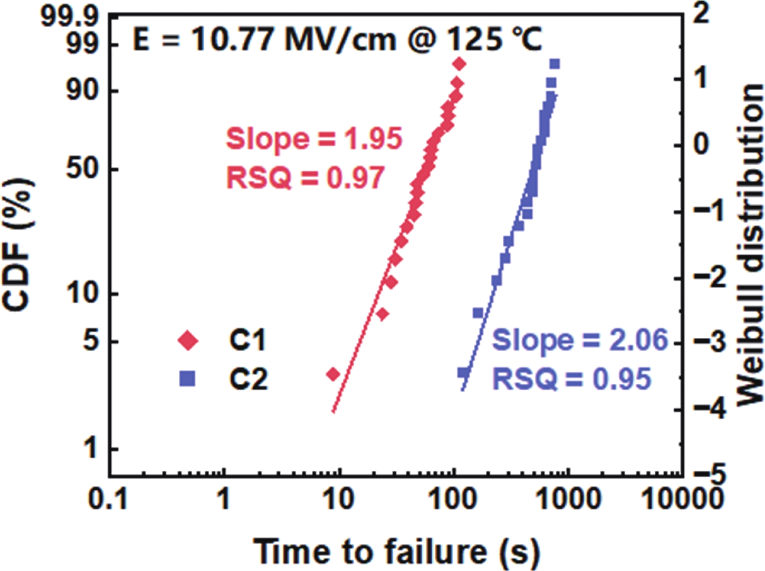
Abstract: Along with NOR flash cell scaling down, dielectric burnout has gradually become one of the most important factors which affects product reliability, especially for high dropout voltage films. In this study, we demonstrate a reliability-enhanced NOR flash cell in 50 nm node technology through structural optimization of floating gate (FG) dimensions and active area profile. By synergistically increasing FG thickness, reducing FG width, and tuning cell-open depth, the control gate-to-active area corner distance expands by 22%, suppressing peak electric fields by 29% vertically and 18% horizontally. This structural innovation achieves: (1) 100× reduction in early-cycle burnout failures, (2) 7.38× time dependent dielectric breakdown lifetime improvement, while maintaining data retention and accelerating programming/erasing speeds by 15.4%/7.3%. The enhanced reliability enables 97.5% reduction in Fowler−Nordheim stress time during characterization program testing, providing a cost-effective solution for automotive-grade flash memories.
Key words: NOR flash, 50 nm, reliability, cell endurance burnout
| [1] |
Chen H L, Liu B T, Gu L. Data retention enhancement of modern 55nm NOR flash memory. 2022 China Semiconductor Technology International Conference, 2022, 1 doi: 10.1109/CSTIC55103.2022.9856863
|
| [2] |
Yu J M, Park J Y, Lee G B, et al. Demonstration of thermally-assisted programming with high speed and improved reliability for junctionless nanowire NOR flash memory. IEEE Trans Nanotechnol, 2019, 18, 1110 doi: 10.1109/TNANO.2019.2945321
|
| [3] |
Sun P, Li Y, Yao Y, et al. Study for NOR flash cell burn out failure improvement in the advanced node below 65nm. 2019 IEEE 13th International Conference on ASIC, 2019, 1 doi: 10.1109/ASICON47005.2019.8983488
|
| [4] |
Chen H L, Tong Y X, Qi X Y, et al. Silicide profile optimization on active area in 4XNM ETOX NOR flash memory. 2023 China Semiconductor Technology International Conference, 2023, 1 doi: 10.1109/CSTIC58779.2023.10219198
|
| [5] |
Du Y H, Gu L, Chen H L, et al. Yield improvement in 4X node technology ETOX NOR flash by optimizing control gate related process and design. 2024 Conference of Science and Technology for Integrated Circuits, 2024, 1 doi: 10.1109/CSTIC61820.2024.10532096
|
| [6] |
Chen C Z, Hu D Y, Wu H M. Effective radiation damage to floating gate of flash memory. 2021 China Semiconductor Technology International Conference, 2021, 1 doi: 10.1109/CSTIC52283.2021.9461408
|
| [7] |
Vargas-Sierra S, Tanios B, González-Luján J J, et al. TID radiation effects of 1Gb cots nor flash memories for the esa juice mission. 2019 19th European Conference on Radiation and Its Effects on Components and Systems, 2019, 1 doi: 10.1109/RADECS47380.2019.9745698
|
| [8] |
Tanios B, Kaddour M, Forgerit B, et al. Single event effects characterization of 55-65nm NOR flash for space applications. 2021 21th European Conference on Radiation and Its Effects on Components and Systems, 2021, 1 doi: 10.1109/RADECS53308.2021.9954491
|
| [9] |
Verma R. Flash memory quality and reliability issues. IEEE International Workshop on Memory Technology, Design and Testing, 1996, 32 doi: 10.1109/MTDT.1996.782488
|
| [10] |
Lenzlinger M, Snow E H. Fowler-Nordheim tunneling into thermally grown SiO2. IEEE Trans Electron Devices, 1968, 15(9), 686 doi: 10.1063/1.1657043
|
| [11] |
Cottrell P E, Troutman R R, Ning T H. Hot-electron emission in N-channel IGFET’s. IEEE Trans Electron Devices, 1979, 26(4), 520 doi: 10.1109/T-ED.1979.19456
|
| [12] |
Eitan B, Frohman-Bentchkowsky D. Hot-electron injection into the oxide in n-channel MOS devices. IEEE Trans Electron Devices, 1981, 28(3), 328 doi: 10.1109/T-ED.1981.20336
|
| [13] |
Lee J S. Review paper: Nano-floating gate memory devices. Electron Mater Lett, 2011, 7(3), 175 doi: 10.1007/s13391-011-0901-5
|
| [14] |
Yang X N, Liu J, Zheng Z W, et al. Impact of P/E cycling on read current fluctuation of NOR Flash memory cell: A microscopic perspective based on low frequency noise analysis. 2015 IEEE International Reliability Physics Symposium, 2015, 5B.7.1 doi: 10.1109/IRPS.2015.7112748
|
| [15] |
Shibata T, Ohmi T. A functional MOS transistor featuring gate-level weighted sum and threshold operations. IEEE Trans Electron Devices, 1992, 39(6), 1444 doi: 10.1109/16.137325
|
| [16] |
Chen H L, Xu R, Wang H, et al. Improvement of disturb and endurance in NOR flash memory. 2022 China Semiconductor Technology International Conference, 2022, 1 doi: 10.1109/CSTIC55103.2022.9856867
|
| [17] |
Ma J Y, Wang L, Liang C D, et al. Structure optimization of 4X NM nor flash for improving cell performance. 2024 Conference of Science and Technology for Integrated Circuits, 2024, 1 doi: 10.1109/CSTIC61820.2024.10532054
|
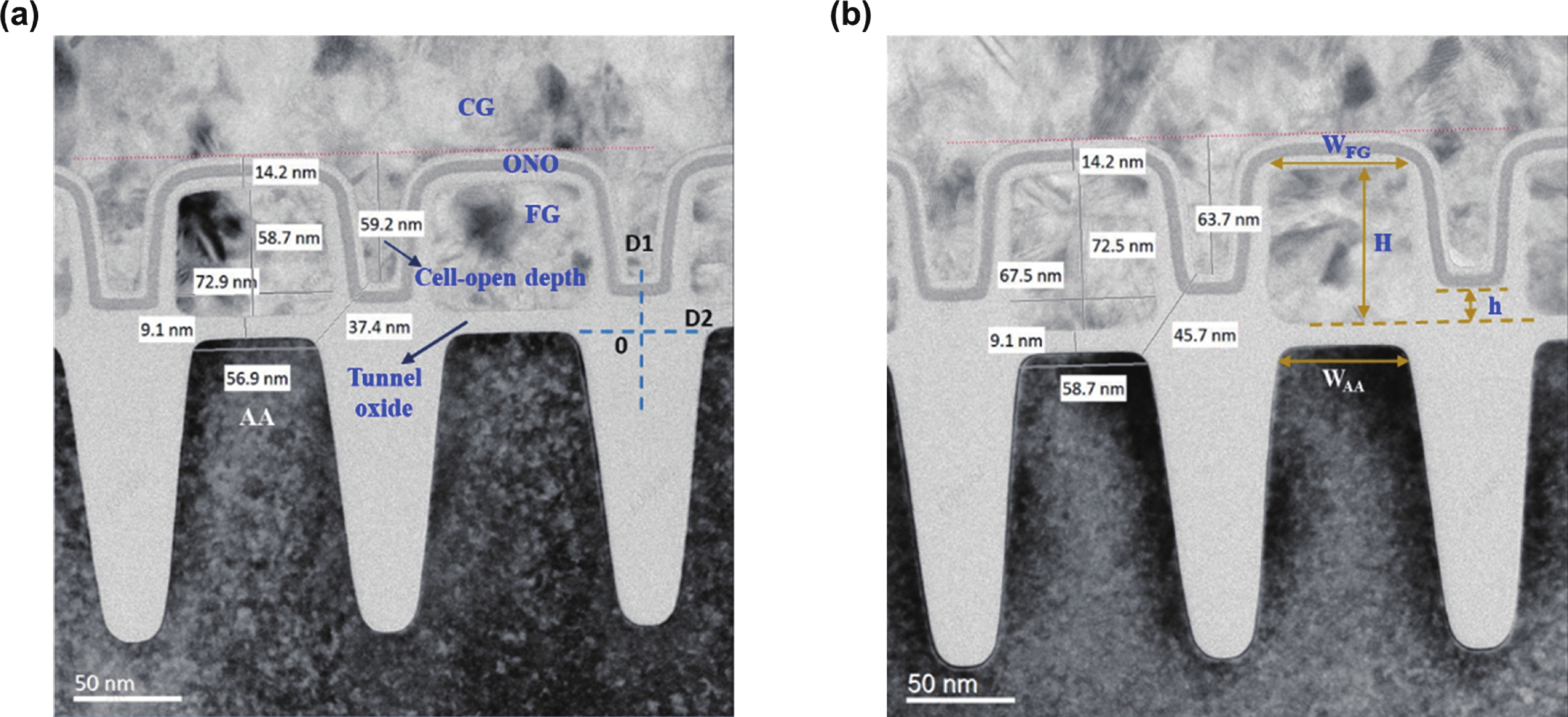
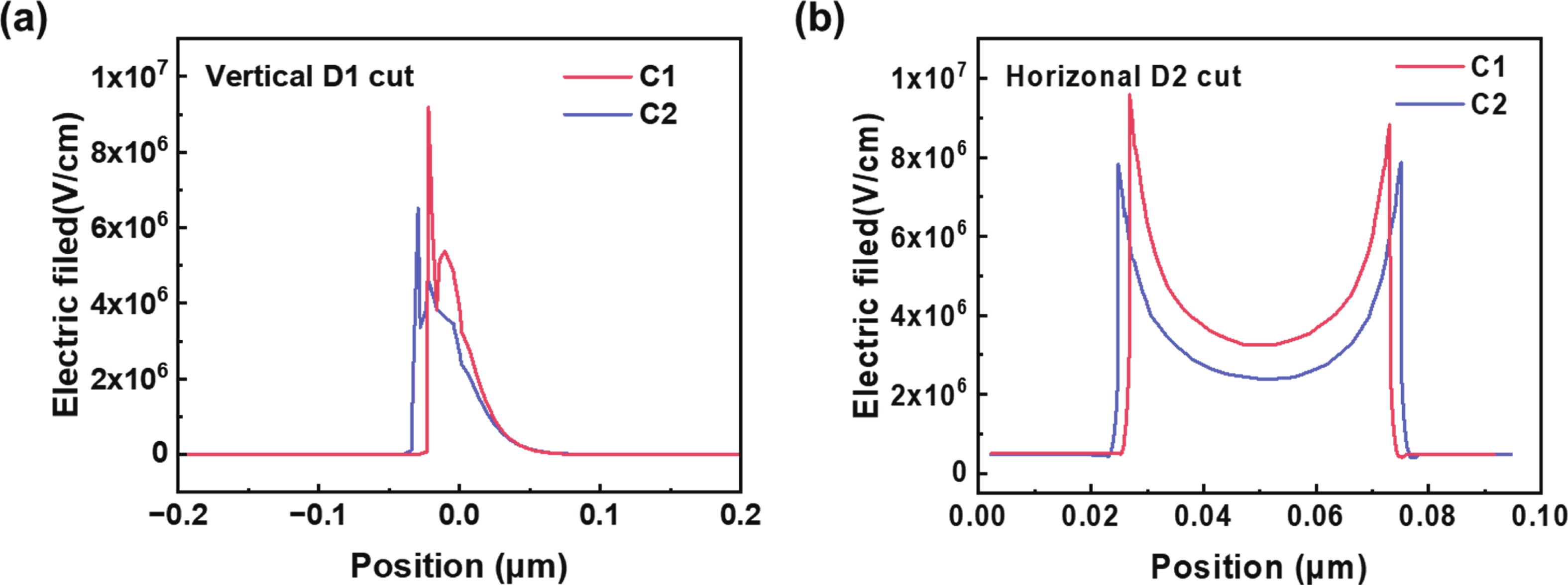
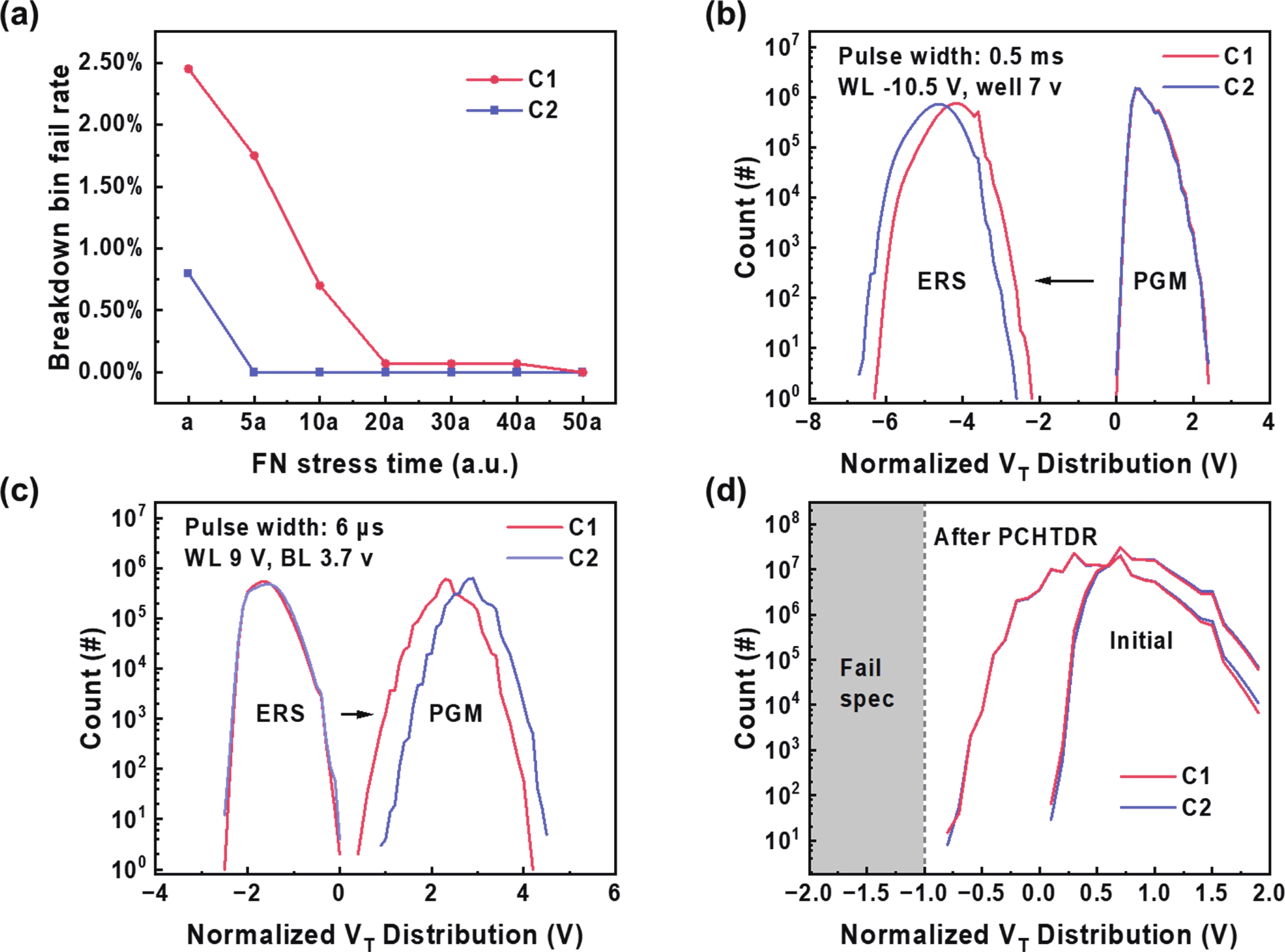
Table 1. Comparison of properties of two NOR flash cell structures C1 and C2.
| Parameter | C1 (old) | C2 (new) | Difference |
| FG thickness (nm) | 58.7 | 72.5 | 23.5% |
| FG width (nm) | 72.9 | 67.5 | −7.4% |
| Cell-open depth (nm) | 59.2 | 63.7 | 7.6% |
| CG-AA corner distance (nm) | 37.4 | 45.7 | 22.2% |
| TCAD vertical e-field peak value (V/cm) | 9.17 × 10⁶ | 6.50 × 10⁶ | −29.1% |
| TCAD horizontal e-field peak value (V/cm) | 9.58 × 10⁶ | 7.82 × 10⁶ | −18.4% |
| CG-AA TDDB T63% lifetime (s) | 68 | 570 | 738% |
| CG-AA burnout failure (PPM) | 1000 | <10 | − |
| PGM speed (V/Pulse) | 3.9 | 4.5 | 15.4% |
| ERS speed (V/Pulse) | 5.5 | 5.9 | 7.3% |
| Data retention (V) | 0.9 | 0.9 | Comparable |
 DownLoad: CSV
Table 2. TCAD model and parameters.
| Item | Content | ||
| Software | Sentaurus TCAD | ||
| Input | Simulation structure | ||
| Main physical model | Quantum model | Quantum potential | |
| Mobility model | Enormal, doping dependence, high field saturation | ||
| Density of states model | Effective intrinsic density (old slot boom) | ||
| Recombination model | SRH (DopingDep) avalanche Band2Band | ||
| Main parameter | Silicon relative permittivity | 11.7 | |
| Silicon electron affinity | 4.0727 eV | ||
| Silicon bandgap | 1.12416 eV | ||
| Silicon mobility-electron | 1.4170 × 103 cm2/(V·s) | ||
| Silicon mobility-hole | 4.7050 × 102 cm2/(V·s) | ||
| Oxide relative permittivity | 3.9 | ||
| Oxide electron affinity | 0.9 eV | ||
| Oxide bandgap | 9.0 eV | ||
| Output | Electric field | ||
DownLoad: CSV
Table 3. Cell structure change experiment.
| Parameter | C1 | DOE1 | DOE2 | DOE3 | DOE4 | DOE5 |
| FG thickness (nm) | 58.7 | 58.7 × 1.235 | 58.7 × 1.235 | 58.7 × 1.235 | 58.7 × 1.235 | 58.7 × 1.235 |
| FG width (nm) | 72.9 | 72.9 × 0.926 | 72.9 × 0.926 | 72.9 × 0.926 | 72.9 × 0.926 | 72.9 × 0.926 |
| Cell-open depth (nm) | 59.2 | 59.2 | 59.2 × 1.022 | 59.2 × 1.076 | 59.2 × 1.103 | 59.2 × 1.136 |
| CG-AA corner distance (nm) | 37.4 | 37.4 × 1.286 | 37.4 × 1.259 | 37.4 × 1.222 | 37.4 × 1.149 | 37.4 × 1.118 |
| Breakdown bin failure rate (%) | 2.5 | 0.8 | 0.82 | 0.8 | 1.13 | 1.75 |
| GCR | 0.342 | 0.318 | 0.335 | 0.362 | 0.388 | 0.438 |
DownLoad: CSV
| [1] |
Chen H L, Liu B T, Gu L. Data retention enhancement of modern 55nm NOR flash memory. 2022 China Semiconductor Technology International Conference, 2022, 1 doi: 10.1109/CSTIC55103.2022.9856863
|
| [2] |
Yu J M, Park J Y, Lee G B, et al. Demonstration of thermally-assisted programming with high speed and improved reliability for junctionless nanowire NOR flash memory. IEEE Trans Nanotechnol, 2019, 18, 1110 doi: 10.1109/TNANO.2019.2945321
|
| [3] |
Sun P, Li Y, Yao Y, et al. Study for NOR flash cell burn out failure improvement in the advanced node below 65nm. 2019 IEEE 13th International Conference on ASIC, 2019, 1 doi: 10.1109/ASICON47005.2019.8983488
|
| [4] |
Chen H L, Tong Y X, Qi X Y, et al. Silicide profile optimization on active area in 4XNM ETOX NOR flash memory. 2023 China Semiconductor Technology International Conference, 2023, 1 doi: 10.1109/CSTIC58779.2023.10219198
|
| [5] |
Du Y H, Gu L, Chen H L, et al. Yield improvement in 4X node technology ETOX NOR flash by optimizing control gate related process and design. 2024 Conference of Science and Technology for Integrated Circuits, 2024, 1 doi: 10.1109/CSTIC61820.2024.10532096
|
| [6] |
Chen C Z, Hu D Y, Wu H M. Effective radiation damage to floating gate of flash memory. 2021 China Semiconductor Technology International Conference, 2021, 1 doi: 10.1109/CSTIC52283.2021.9461408
|
| [7] |
Vargas-Sierra S, Tanios B, González-Luján J J, et al. TID radiation effects of 1Gb cots nor flash memories for the esa juice mission. 2019 19th European Conference on Radiation and Its Effects on Components and Systems, 2019, 1 doi: 10.1109/RADECS47380.2019.9745698
|
| [8] |
Tanios B, Kaddour M, Forgerit B, et al. Single event effects characterization of 55-65nm NOR flash for space applications. 2021 21th European Conference on Radiation and Its Effects on Components and Systems, 2021, 1 doi: 10.1109/RADECS53308.2021.9954491
|
| [9] |
Verma R. Flash memory quality and reliability issues. IEEE International Workshop on Memory Technology, Design and Testing, 1996, 32 doi: 10.1109/MTDT.1996.782488
|
| [10] |
Lenzlinger M, Snow E H. Fowler-Nordheim tunneling into thermally grown SiO2. IEEE Trans Electron Devices, 1968, 15(9), 686 doi: 10.1063/1.1657043
|
| [11] |
Cottrell P E, Troutman R R, Ning T H. Hot-electron emission in N-channel IGFET’s. IEEE Trans Electron Devices, 1979, 26(4), 520 doi: 10.1109/T-ED.1979.19456
|
| [12] |
Eitan B, Frohman-Bentchkowsky D. Hot-electron injection into the oxide in n-channel MOS devices. IEEE Trans Electron Devices, 1981, 28(3), 328 doi: 10.1109/T-ED.1981.20336
|
| [13] |
Lee J S. Review paper: Nano-floating gate memory devices. Electron Mater Lett, 2011, 7(3), 175 doi: 10.1007/s13391-011-0901-5
|
| [14] |
Yang X N, Liu J, Zheng Z W, et al. Impact of P/E cycling on read current fluctuation of NOR Flash memory cell: A microscopic perspective based on low frequency noise analysis. 2015 IEEE International Reliability Physics Symposium, 2015, 5B.7.1 doi: 10.1109/IRPS.2015.7112748
|
| [15] |
Shibata T, Ohmi T. A functional MOS transistor featuring gate-level weighted sum and threshold operations. IEEE Trans Electron Devices, 1992, 39(6), 1444 doi: 10.1109/16.137325
|
| [16] |
Chen H L, Xu R, Wang H, et al. Improvement of disturb and endurance in NOR flash memory. 2022 China Semiconductor Technology International Conference, 2022, 1 doi: 10.1109/CSTIC55103.2022.9856867
|
| [17] |
Ma J Y, Wang L, Liang C D, et al. Structure optimization of 4X NM nor flash for improving cell performance. 2024 Conference of Science and Technology for Integrated Circuits, 2024, 1 doi: 10.1109/CSTIC61820.2024.10532054
|


Article views: 684 Times PDF downloads: 206 Times Cited by: 0 Times
Received: 15 March 2025 Revised: 20 May 2025 Online: Accepted Manuscript: 20 June 2025Uncorrected proof: 23 July 2025Published: 15 December 2025
| Citation: |
Kevin Fang, Wei Wang, Yibai Xue, Fan Wang, Dong Pan, Yi Li, Jerry Zhou. A high reliability NOR flash cell in 50 nm node technology[J]. Journal of Semiconductors, 2025, 46(12): 122301. doi: 10.1088/1674-4926/25030030
****
K Fang, W Wang, Y B Xue, F Wang, D Pan, Y Li, and J Zhou, A high reliability NOR flash cell in 50 nm node technology[J]. J. Semicond., 2025, 46(12), 122301 doi: 10.1088/1674-4926/25030030

|
 Kevin Fang got his bachelor’s degree in 2003 from Tongji University and his master’s degree in 2011 from Huazhong University of Science and Technology. Now he is a doctoral student at Huazhong University of Science and Technology under the supervision of Prof. Yi Li. His research focuses on reliability issues of 50 nm floating gate NOR flash memory products
 Yi Li currently serves as a professor at Huazhong University of Science and Technology (HUST). He obtained his PhD in microelectronics from HUST in 2014. His primary research interests are centered on memristors and their applications in the realms of in-memory computing and neuromorphic computing
 Jerry Zhou got his bachelor’s degree in 2004 from Wuhan University of Technology and his master’s degree in 2014 from Wuhan University. He is currently a doctoral student at Huazhong University of Science and Technology. His research focuses on non-volatile memory process and reliability research
| [1] |
Chen H L, Liu B T, Gu L. Data retention enhancement of modern 55nm NOR flash memory. 2022 China Semiconductor Technology International Conference, 2022, 1 doi: 10.1109/CSTIC55103.2022.9856863
|
| [2] |
Yu J M, Park J Y, Lee G B, et al. Demonstration of thermally-assisted programming with high speed and improved reliability for junctionless nanowire NOR flash memory. IEEE Trans Nanotechnol, 2019, 18, 1110 doi: 10.1109/TNANO.2019.2945321
|
| [3] |
Sun P, Li Y, Yao Y, et al. Study for NOR flash cell burn out failure improvement in the advanced node below 65nm. 2019 IEEE 13th International Conference on ASIC, 2019, 1 doi: 10.1109/ASICON47005.2019.8983488
|
| [4] |
Chen H L, Tong Y X, Qi X Y, et al. Silicide profile optimization on active area in 4XNM ETOX NOR flash memory. 2023 China Semiconductor Technology International Conference, 2023, 1 doi: 10.1109/CSTIC58779.2023.10219198
|
| [5] |
Du Y H, Gu L, Chen H L, et al. Yield improvement in 4X node technology ETOX NOR flash by optimizing control gate related process and design. 2024 Conference of Science and Technology for Integrated Circuits, 2024, 1 doi: 10.1109/CSTIC61820.2024.10532096
|
| [6] |
Chen C Z, Hu D Y, Wu H M. Effective radiation damage to floating gate of flash memory. 2021 China Semiconductor Technology International Conference, 2021, 1 doi: 10.1109/CSTIC52283.2021.9461408
|
| [7] |
Vargas-Sierra S, Tanios B, González-Luján J J, et al. TID radiation effects of 1Gb cots nor flash memories for the esa juice mission. 2019 19th European Conference on Radiation and Its Effects on Components and Systems, 2019, 1 doi: 10.1109/RADECS47380.2019.9745698
|
| [8] |
Tanios B, Kaddour M, Forgerit B, et al. Single event effects characterization of 55-65nm NOR flash for space applications. 2021 21th European Conference on Radiation and Its Effects on Components and Systems, 2021, 1 doi: 10.1109/RADECS53308.2021.9954491
|
| [9] |
Verma R. Flash memory quality and reliability issues. IEEE International Workshop on Memory Technology, Design and Testing, 1996, 32 doi: 10.1109/MTDT.1996.782488
|
| [10] |
Lenzlinger M, Snow E H. Fowler-Nordheim tunneling into thermally grown SiO2. IEEE Trans Electron Devices, 1968, 15(9), 686 doi: 10.1063/1.1657043
|
| [11] |
Cottrell P E, Troutman R R, Ning T H. Hot-electron emission in N-channel IGFET’s. IEEE Trans Electron Devices, 1979, 26(4), 520 doi: 10.1109/T-ED.1979.19456
|
| [12] |
Eitan B, Frohman-Bentchkowsky D. Hot-electron injection into the oxide in n-channel MOS devices. IEEE Trans Electron Devices, 1981, 28(3), 328 doi: 10.1109/T-ED.1981.20336
|
| [13] |
Lee J S. Review paper: Nano-floating gate memory devices. Electron Mater Lett, 2011, 7(3), 175 doi: 10.1007/s13391-011-0901-5
|
| [14] |
Yang X N, Liu J, Zheng Z W, et al. Impact of P/E cycling on read current fluctuation of NOR Flash memory cell: A microscopic perspective based on low frequency noise analysis. 2015 IEEE International Reliability Physics Symposium, 2015, 5B.7.1 doi: 10.1109/IRPS.2015.7112748
|
| [15] |
Shibata T, Ohmi T. A functional MOS transistor featuring gate-level weighted sum and threshold operations. IEEE Trans Electron Devices, 1992, 39(6), 1444 doi: 10.1109/16.137325
|
| [16] |
Chen H L, Xu R, Wang H, et al. Improvement of disturb and endurance in NOR flash memory. 2022 China Semiconductor Technology International Conference, 2022, 1 doi: 10.1109/CSTIC55103.2022.9856867
|
| [17] |
Ma J Y, Wang L, Liang C D, et al. Structure optimization of 4X NM nor flash for improving cell performance. 2024 Conference of Science and Technology for Integrated Circuits, 2024, 1 doi: 10.1109/CSTIC61820.2024.10532054
|

 WeChat ID
Journal of Semiconductors © 2017 All Rights Reserved 京ICP备05085259号-2