Engineering characterization of water has produced huge varieties of materials with special properties to meet human needs. Equilibrium properties of water-based liquids are well understood via localized atomic and molecular orbital theories. However, the mechanism of electrical conductivity of pure water has proven elusive. We show here it is trapping limited drift of positive and negative quasi-protons (or protons and proton-vacancies) on the extended water lattice, which is accounted for by the long-range correlation inherent in the Fermion (electrons and protons) and Boson (phonons) energy band theory of quasi-particles in solids, with vigorous adherence to equilibrium and nonequilibrium states.
Issue Browser
Volume 34, Issue 12,
Dec 2013


J. Semicond.
2013, 34(12): 122001 doi: 10.1088/1674-4926/34/12/122001

The transition among multiple charging states of a semiconductor's localized intrinsic/impurity defects is considered as phase transitions, and the concept of transition Gibbs free energy level (TGFEL) is proposed. Dependence of the cross section of TGFEL on its charge state is discussed. Introduction of TGFEL to replace activation energy has fundamentally important consequences for semiconductor physics and devices. TGFEL involves entropy. What is to be included and not included in the entropy term consistently for all defect levels is an unresolved open question, related to correct interpretation of various experimental data associated with various defect levels. This work is a first step towards resolving this question.


J. Semicond.
2013, 34(12): 122002 doi: 10.1088/1674-4926/34/12/122002

Electron Raman scattering (ERS) is investigated in a spherical HgS/CdS quantum dot quantum well (QDQW). The differential cross section (DCS) is calculated as a function of the scattering frequency and the sizes of QDQW. Single parabolic conduction and valence bands are assumed. The selection rules for the processes are studied. Singularities in the spectra are found and interpreted. The ERS studied here can be used to provide direct information about the electron band structure of these systems.


J. Semicond.
2013, 34(12): 122003 doi: 10.1088/1674-4926/34/12/122003

We have measured the in-plane optical anisotropy (IPOA) of (1120) ZnO (a-plane) on (1012) sapphire (r-plane) by reflectance difference spectroscopy (RDS) at room temperature. Giant IPOA has been observed between the light polarized direction parallel and perpendicular to the c axis of ZnO, since the symmetry of a-plane is C2v. A sharp resonance has been observed near the fundamental band gap, which is induced by the polarization-depend band gap shift. The sharp line shape is attributed to the exciton transition. The spectra fitting and differential spectra indicate the polarization-depend band energies. The giant IPOA is possible enhanced by anisotropy strain along and perpendicular to the c axis in the a-plane.


J. Semicond.
2013, 34(12): 123001 doi: 10.1088/1674-4926/34/12/123001

Uniform GaN nanopillar arrays have been successfully fabricated by inductively coupled plasma etching using self-organized nickel nano-islands as the masks on GaN/sapphire. GaN nanopillars with diameters of 350 nm and densities of 2.6×108 cm-2 were demonstrated and controlled by the thickness of Ni film and the NH3 annealing time. These GaN nanopillars show improved optical properties and strain change compared to that of GaN film before ICP etching. Such structures with large-area uniformity and high density could provide additional advantages for light emission of light-emitting diodes, quality improvement of ELO regrowth, etc.


J. Semicond.
2013, 34(12): 123002 doi: 10.1088/1674-4926/34/12/123002

The electrical properties of Ni0.95Pt0.05-germanosilicide/Si1-xGex contacts on heavily doped p-type strained Si1-xGex layers as a function of composition and doping concentration for a given composition have been investigated. A four-terminal Kelvin-resistor structure has been fabricated by using the conventional complementary metal-oxide-semiconductor (CMOS) process to measure contact resistance. The results showed that the contact resistance of the Ni0.95Pt0.05-germanosilicide/Si1-xGex contacts slightly reduced with increasing the Ge fraction. The higher the doping concentration, the lower the contact resistivity. The contact resistance of the samples with doping concentration of 4×1019 cm-3 is nearly one order of magnitude lower than that of the samples with doping concentration of 5×1017 cm-3. In addition, the influence of dopant segregation on the contact resistance for the lower doped samples is larger than that for the higher doped samples.


J. Semicond.
2013, 34(12): 124001 doi: 10.1088/1674-4926/34/12/124001

A high performance trench insulated gate bipolar transistor which combines a semi-superjunction structure and an accumulation channel (sSJTAC-IGBT) is proposed for the first time. Compared with the TAC-IGBT, the new device not only retains the advantages of the accumulation channel, but also obtains a larger breakdown voltage (BV), a faster turn-off speed and a smaller saturation current level while keeping the on-state voltage drop lower as the TAC-IGBT does as well. Therefore, the new structure enlarges the short circuit safe operating area (SCSOA) and reduces the energy loss during the turn-off process.


J. Semicond.
2013, 34(12): 124002 doi: 10.1088/1674-4926/34/12/124002

The effects of linear doping profile near the source and drain contacts on the switching and high-frequency characteristics for conventional single-material-gate CNTFET (C-CNTFET) and hetero-material-gate CNTFET (HMG-CNTFET) have been theoretically investigated by using a quantum kinetic model. This model is based on two-dimensional non-equilibrium Green's functions (NEGF) solved self-consistently with Poisson's equations. The simulation results show that at a CNT channel length of 20 nm with chirality (7, 0), the intrinsic cutoff frequency of C-CNTFETs reaches up to a few THz. In addition, a comparison study has been performed between C-and HMG-CNTFETs. For the C-CNTFET, results reveal that a longer linear doping length can improve the cutoff frequency and switching speed. However, it has the reverse effect on on/off current ratios. To improve the on/off current ratios performance of CNTFETs and overcome short-channel effects (SCEs) in high-performance device applications, a novel CNTFET structure with a combination of an HMG and linear doping profile has been proposed. It is demonstrated that the HMG structure design with an optimized linear doping length has improved high-frequency and switching performances as compared to C-CNTFETs. The simulation study may be useful for understanding and optimizing high-performance of CNTFETs and assessing the reliability of CNTFETs for prospective applications.


J. Semicond.
2013, 34(12): 124003 doi: 10.1088/1674-4926/34/12/124003

To enhance the robustness of LDMOS ESD protection devices, the influence of a source-bulk layout structure is analyzed by theoretical analysis and numerical simulation. Novel structures with varied source-bulk layout structures are fabricated and compared. As demonstrated by TLP testing, the optimized structure has an 88% larger It2 than a conventional one, and its Vt1 is reduced from 55.53 to 50.69 V.


J. Semicond.
2013, 34(12): 124004 doi: 10.1088/1674-4926/34/12/124004

In this paper, the enhanced performance of InGaN/GaN multiple quantum well solar cells grown on patterned sapphire substrates (PSS) was demonstrated. The short-circuit current (Jsc) density of the solar cell grown on PSS showed an improvement of 60%, compared to that of solar cells grown on conventional sapphire substrate. The improved performance is primarily due to the reduction of edge dislocations and the increased light absorption path by the scattering from the textured surface of the PSS. It shows that the patterned sapphire technology can effectively alleviate the problem of high-density dislocations and low Jsc caused by thinner absorption layers of the InGaN based solar cell, and it is promising to improve the efficiency of the solar cell.


J. Semicond.
2013, 34(12): 124005 doi: 10.1088/1674-4926/34/12/124005

Conventional GaN-based flip-chip light-emitting diodes (CFC-LEDs) use Au bumps to contact the LED chip and Si submount, however the contact area is constrained by the number of Au bumps, limiting the heat dissipation performance. This paper presents a flat surface high power GaN-based flip-chip light emitting diode (SFC-LED), which can greatly improve the heat dissipation performance of the device. In order to understand the thermal performance of the SFC-LED thoroughly, a 3-D finite element model (FEM) is developed, and ANSYS is used to simulate the thermal performance. The temperature distributions of the SFC-LED and the CFC-LED are shown in this article, and the junction temperature simulation values of the SFC-LED and the CFC-LED are 112.80℃ and 122.97℃, respectively. Simulation results prove that the junction temperature of the new structure is 10.17℃ lower than that of the conventional structure. Even if the CFC-LED has 24 Au bumps, the thermal resistance of the new structure is still far less than that of the conventional structure. The SFC-LED has a better thermal property.


J. Semicond.
2013, 34(12): 124006 doi: 10.1088/1674-4926/34/12/124006

A digital-to-analog converter (DAC) in CBCMOS technology was irradiated by 60Co γ-rays at various dose rates and biases for investigating the ionizing radiation response of the DAC. The radiation responses show that the function curve and the key electrical parameters of the DAC in CBCMOS technology are sensitive to total dose and dose rates. Under different bias conditions, the radiation failure levels were different, and the radiation damage under operation bias conditions was more severe. Finally, test results were preliminarily analyzed by relating the failure mode to DAC architecture and process technology.


J. Semicond.
2013, 34(12): 125001 doi: 10.1088/1674-4926/34/12/125001
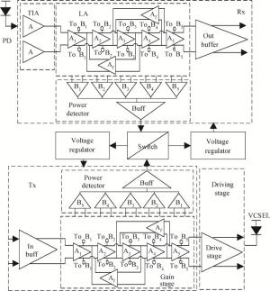
A power-aware transceiver for half-duplex bidirectional chip-to-chip optical interconnects has been designed and fabricated in a 0.13 μm complementary metal-oxide-semiconductor (CMOS) technology. The transceiver can detect the presence and absence of received signals and saves 55% power in Rx enabled mode and 45% in Tx enabled mode. The chip occupies an area of 1.034 mm2 and achieves a 3-dB bandwidth of 6 GHz and 7 GHz in Tx and Rx modes, respectively. The disabled outputs for the Tx and Rx modes are isolated with 180 dB and 139 dB, respectively, from the enabled outputs. Clear eye diagrams are obtained at 4.25 Gbps for both the Tx and Rx modes.


J. Semicond.
2013, 34(12): 125002 doi: 10.1088/1674-4926/34/12/125002

A 2V-10A fast transient response DC-DC buck controller based on fixed frequency hysteresis control is presented. A carefully designed output voltage filter detects the output capacitor current change which helps the controller to respond immediately after load changes. Adaptive hysteresis control guarantees the switching frequency to be the same as the reference frequency by using a CCⅡ-composed circuit and current mirrors. The controller is designed and fabricated in a TSMC 0.35 μm process. Simulation and test results show that this controller achieves a 20 μs settling time in one single switching cycle when load current changes from 1 A to the full load condition at 10 A.


J. Semicond.
2013, 34(12): 125003 doi: 10.1088/1674-4926/34/12/125003

A W-band two-stage amplifier MMIC has been developed using a fully passivated 2×20 μm gate-width and 0.15 μm gate-length InP-based high electron mobility transistor (HEMT) technology. The two-stage amplifier has been realized in combination with a coplanar waveguide technique and cascode topology, thus leading to a compact chip-size of 1.85×0.932 mm2 and an excellent small-signal gain of 25.7 dB at 106 GHz. Additionally, an inter-digital coupling capacitor blocks low-frequency signal, thereby enhancing the stability of the amplifier. The successful design of the two-stage amplifier MMIC indicates that InP HEMT technology has a great potential for W-band applications.


J. Semicond.
2013, 34(12): 125004 doi: 10.1088/1674-4926/34/12/125004

W-band quartz based high output power fix-tuned doublers are analyzed and designed with planar Schottky diodes. Full-wave analysis is carried out to find diode embedding impedances with a lumped port to model the nonlinear junction. Passive networks of the circuit, such as the low pass filter, the E-plane waveguide to strip transitions, input and output matching networks, and passive diode parts are analyzed by using electromagnetic simulators, and the different parts are then combined and optimized together. The exported S-parameters of the doubler circuit are used for multiply efficiency analysis. The highest measured output power is 29.5 mW at 80 GHz and higher than 15 mW in 76-94 GHz. The highest measured efficiency is 11.5% at 92.5 GHz, and the typical value is 6.0% in 70-100 GHz.


J. Semicond.
2013, 34(12): 125005 doi: 10.1088/1674-4926/34/12/125005

A novel transformer-type variable inductor is proposed to achieve a wide tuning range at frequencies as high as K band. The variable inductor is designed, and an intuitive model is built to analyze its performance by HFSS. A lot of mathematical analysis is done in detail. A VCO using the proposed variable inductor is designed with TSMC 0.13 μm CMOS technology for verification. The frequency tuning range of the VCO depends on the proposed variable inductor. The phase noise of the VCO depends on the quality of the LC tank (including the proposed variable inductor and varactors). So a specific AMOS varactor is implemented to improve its quality factor. The VCO is simulated at three typical TSMC fabrication corners (TT, FF, SS) to predict its measure results. The post simulation results shows that the VCO achieves a 20-25.5 GHz continuous tuning range. Its phase noise results at 1 MHz offset are -108.4 dBc/Hz and -100.5 dBc/Hz respectively at the tuning frequencies of 19.6 GHz and 25.5 GHz. The VCO draws only 3 to 6 mA from a 1.2 V power supply.


J. Semicond.
2013, 34(12): 125006 doi: 10.1088/1674-4926/34/12/125006

This paper presents a readout system for the passive pressure sensors which consist of a pressure-sensitive capacitor and an inductance coil to form an LC circuit. The LC circuit transforms the pressure variation into the LC resonant frequency shift. The proposed system is composed of a reader antenna inductively coupled to the sensor inductor, a measurement circuit, and a PC post-processing unit. The measurement circuit generates a DC output voltage related to the sensor's resonant frequency and converts the output voltage into digital form. The PC post-processing unit processes the digital data and calculates the sensor's resonant frequency. To test the performance of the readout system, a sensor is designed and fabricated based on low temperature co-fired ceramic (LTCC), and a series of testing experiments is carried out. The experimental results show good agreement with the impedance analyzer's results, their error is less than 2.5%, and the measured values are almost insensitive to the variation of readout distance. It proves that the proposed system is effective practically.


J. Semicond.
2013, 34(12): 125007 doi: 10.1088/1674-4926/34/12/125007

We present a 10 Gsps 8 bit digital-to-analog converter (DAC) with a novel built-in self-test (BIST) circuit, which makes it possible to evaluate the DAC's performance without a complicated test setup. Design considerations and test results are included. According to the test results, the DAC core and the BIST circuit are able to work under 10 GHz. The chip is fabricated in 0.18 μm SiGe HBTs with ft of 100 GHz. The DAC core occupies a die size of 260×250 μm2.


J. Semicond.
2013, 34(12): 125008 doi: 10.1088/1674-4926/34/12/125008

Coplanar waveguides (CPW) are widely used in mm-wave circuits designs for their good performance. A novel unified model of various on chip CPWs for mm-wave application, together with corresponding direct parameter extraction methodologies, are proposed and investigated, where standard CPW, grounded CPW (GCPW) and CPW with slotted shield (SCPW) are included. Several kinds of influences of different structures are analyzed and considered into the model to explain the frequency-dependent per-unit-length L, C, R, and G parameters, among which the electromagnetic coupling for CPWs with large lower ground or shield is described by a new C-L-R series path in the parallel branch. The direct extraction procedures are established, which can ensure both accuracy and simplicity compared with other reported methods. Different CPWs are fabricated and measured on 90-nm CMOS processes with Short-Open-Load-Through (SOLT) de-embedding techniques. Excellent agreement between the model and the measured data for different CPWs is achieved up to 67 GHz.


J. Semicond.
2013, 34(12): 125009 doi: 10.1088/1674-4926/34/12/125009

This paper presents a continuous-time analog interface ASIC for use in MEMS gyroscopes. A charge sensitive amplifier with a chopper stabilization method is adopted to suppress the low-frequency noise. In order to cancel the effect caused by the gyroscope capacitive mismatch, a mismatch auto-compensation circuit is implemented. The gain and phase shift of the drive closed loop is controlled separately by an auto gain controller and an adjustable phase shifter. The chip is fabricated in a 0.35 μm CMOS process. The test of the chip is performed with a vibratory gyroscope, and the measurement shows that the noise floor is 0.003°/s/$\sqrt {{\rm{Hz}}}$, and the measured drift stability is 43°/h. Within -300 to 300°/s of rotation rate input range, the non-linearity is less than 0.1%.


J. Semicond.
2013, 34(12): 125010 doi: 10.1088/1674-4926/34/12/125010

This paper presents a 0.18 μm CMOS 6.25 Gb/s equalizer for high speed backplane communication. The proposed equalizer is a combined one consisting of a one-tap feed-forward equalizer (FFE) and a two-tap half-rate decision feedback equalizer (DFE) in order to cancel both pre-cursor and post-cursor ISI. By employing an active-inductive peaking circuit for the delay line, the bandwidth of the FFE is increased and the area cost is minimized. CML-based circuits such as DFFs, summers and multiplexes all help to improve the speed of DFEs. Measurement results illustrate that the equalizer operates well when equalizing 6.25 Gb/s data is passed over a 30-inch channel with a loss of 22 dB and consumes 55.8 mW with the supply voltage of 1.8 V. The overall chip area including pads is 0.3×0.5 mm2.


J. Semicond.
2013, 34(12): 125011 doi: 10.1088/1674-4926/34/12/125011

This paper presents a new poly-Si pixel circuit employing AC driving mode for active matrix organic light-emitting diode (AMOLED) displays. The proposed pixel circuit, which consists of one driving thin-film transistor (TFT), three switching TFTs, and one storage capacitor, can effectively compensate for the threshold voltage variation in poly-Si and the OLED degradation. As there is no light emission, except for during the emitting period, and a small number of devices used in the proposed pixel circuit, a high contrast ratio and a high pixel aperture ratio can be easily achieved. Simulation results by SMART-SPICE software show that the non-uniformity of the OLED current for the proposed pixel circuit is significantly decreased ( < 10%) with an average value of 2.63%, while that of the conventional 2T1C is 103%. Thus the brightness uniformity of AMOLED displays can be improved by using the proposed pixel circuit.


J. Semicond.
2013, 34(12): 125012 doi: 10.1088/1674-4926/34/12/125012

It is very important to detect transition-delay faults and stuck-at faults in system on chip (SoC) under 90 nm processing technology, and the transition-delay faults can only be detected by using an at-speed testing method. In this paper, an on-chip clock (OCC) controller with a bypass function based on an internal phase-locked loop is designed to test faults in SoC. Furthermore, a clock chain logic which can eliminate the metastable state is realized to generate an enable signal for the OCC controller, and then, the test pattern is generated by automatic test pattern generation (ATPG) tools. Next, the scan test pattern is simulated by using the Synopsys tool and the correctness of the design is verified. The result shows that the design of an at-speed scan test in this paper is highly efficient for detecting timing-related defects. Finally, the 89.29% transition-delay fault coverage and the 94.50% stuck-at fault coverage are achieved, and it is successfully applied to an integrated circuit design.


J. Semicond.
2013, 34(12): 126001 doi: 10.1088/1674-4926/34/12/126001

CMP process optimization for bulk copper removal based on alkaline copper slurry was performed on a 300 mm Applied Materials Reflexion LK system. Under the DOE condition, we conclude that as the pressure increases, the removal rate increases and non-uniformity is improved. As the slurry flow rate increases, there is no significant improvement in the material removal rate, but it does slightly reduce the WIWNU and thus improve uniformity. The optimal variables are obtained at a reduced pressure of 1.5 psi and a slurry flow rate of 300 ml/min. Platen/carrier rotary speed is set at a constant value of 97/103 rpm. We obtain optimized CMP characteristics including a removal rate over 6452 Å/min and non-uniformity below 4% on blanket wafer and the step height is reduced by nearly 8000 Å/min in the center of the wafer on eight layers of copper patterned wafer, the surface roughness is reduced to 0.225 nm.