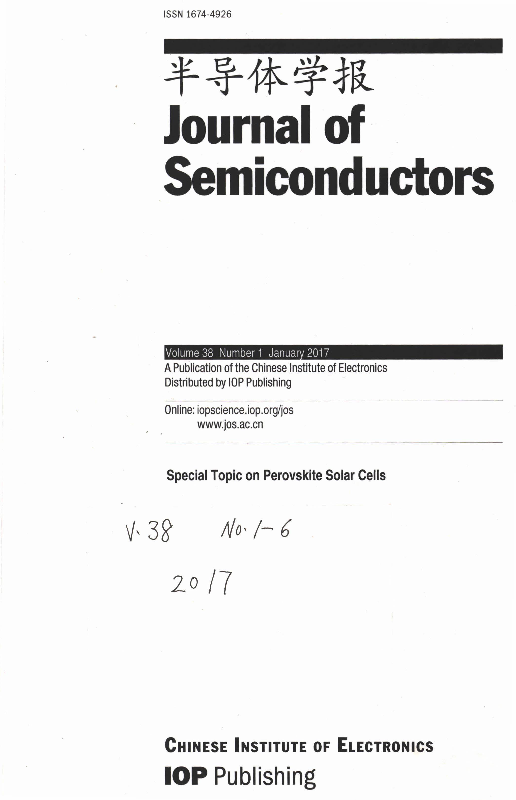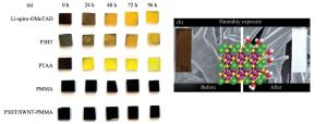
Perovskite solar cells have attracted significant attention in just the past few years in solar cell research fields, where the power conversion efficiency was beyond 22. 1%. Now, the most important challenge for perovskite solar cells in practical applications is the stability issue. In this mini-review, we will summarize the degradation mechanism of perovskite solar cells, including the perovskite material itself and also the interfaces. While we also provide our opinion on improving the stability of perovskite solar cells.
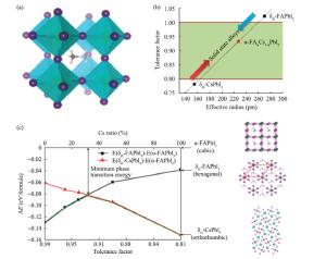
Perovskite solar cells have experienced an unprecedented rapid development in the power conversion efficiency (PCE) during the past 7 years, and the record PCE has been already comparable to the traditional polycrystalline silicon solar cells. Presently, it is more urgent to address the challenge on device stability for the future commercial application. Recently, the inorganic cesium lead halide perovskite has been intensively studied as one of the alternative candidates to improve device stability through controlling the phase transition. The cesium (Cs)-doped perovskites show more superior stability comparing with organic methylammonium (MA) lead halide perovskite or formamidinium (FA) lead halide perovskite. Here, recent progress of the inorganic cesium application in organic-inorganic perovskite solar cells (PSCs) is highlighted from the viewpoints of the device efficiency and the device stability.
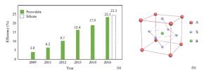
The lead halide-based perovskites, for instance, CH3NH3PbX3 and CsPbX3 (X=Cl, Br, I), have received a lot of attention. Compared with bulk materials, low-dimensional perovskites have demonstrated a range of unique optical, electrical and mechanical properties, which enable wide applications in solar cells, lasers and other optoelectronic devices. In this paper, we provide a summary of the research progress of the low-dimensional perovskites in recent years, from synthesis methods, basic properties to their optoelectronic applications.
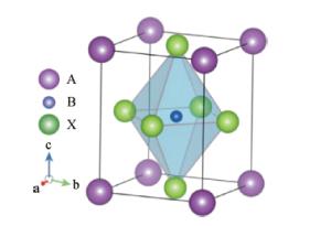
Organic-inorganic hybrid perovskite solar cells have undergone especially intense research and transformation over the past seven years due to their enormous progress in conversion efficiencies. In this perspective, we review the latest developments of conventional perovskite solar cells with a main focus on dopant-free organic hole transporting materials (HTMs). Regarding the rapid progress of perovskite solar cells, stability of devices using dopant-free HTMs are also discussed to help readers understand the challenges and opportunities in high performance and stable perovskite solar cells .

The close-to-optimal band gap, large absorption coefficient, low manufacturing cost and rapid increase in power conversion efficiency make the organic-inorganic hybrid halide (CH3NH3PbI3) and related perovskite solar cells very promising for commercialization. The properties of point defects in the absorber layer semiconductors have important influence on the photovoltaic performance of solar cells, so the investigation on the defect properties in the perovskite semiconductors is necessary for the optimization of their photovoltaic performance. In this work, we give a brief review to the first-principles calculation studies on the defect properties in a series of perovskite semiconductors, including the organic-inorganic hybrid perovskites and inorganic halide perovskites. Experimental identification of these point defects and characterization of their properties are called for.
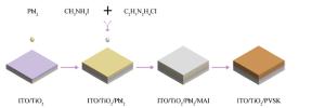
Here, we introduced acetamidine (C2H3N2H3, Aa)-based salt as an additive in the fabrication of perovskite (CH3NH3PbI3) layer for perovskite solar cells. It was found that as an amidine-based salt, this additive successfully enhanced the crystallinity of CH3NH3PbI3 and helped to form smooth and uniform films with comparable grain size and full coverage. Besides, perovskite film with additive showed a much longer carrier lifetime and an obviously enhanced open-circuit voltage in the corresponding devices, indicating that the acetamidine-based salt can reduce the carrier recombination in both the film and device. We further demonstrate a promising perovskite device based on acetamidine salt by using a configuration of ITO/TiO2/Perovskite/Spiro-OMeTAD/Au under < 150℃ fabrication condition. A power conversion efficiency (PCE) of 16.54% was achieved, which is much higher than the control device without acetamidine salt. These results present a simple method for film quality optimization of perovskite to further improve photovoltaic performances of perovskite solar cells, which may also benefit the exploration of A cation in perovskite materials.
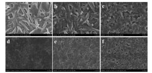
The fast developing perovskite solar cells shows high efficiency and low cost. However, the stability problem restricts perovskite from commercial use. In this work, we have studied the effect of grain orientation on the morphological stability of perovskite thin films. By tuning the inorganic/organic ratio in the precursor solution, perovskite thin films with both high crystallinity and good morphological stability have been fabricated. The thermal stability of perovskite solar cells based on the optimized films has been tested. The device performance shows no degradation after annealing at 100℃ for 5 h in air. This finding provides general guidelines for the development of thermally stable perovskite solar cells.
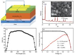
A rising candidate for upgrading the performance of an established narrow-bandgap solar technology without adding much cost is to construct the tandem solar cells from a crystalline silicon bottom cell and a high open-circuit voltage top cell. Here, we present a four-terminal tandem solar cell architecture consisting of a self-filtered planar architecture perovskite top cell and a silicon heterojunction bottom cell. A transparent ultrathin gold electrode has been used in perovskite solar cells to achieve a semi-transparent device. The transparent ultrathin gold contact could provide a better electrical conductivity and optical reflectance-scattering to maintain the performance of the top cell compared with the traditional metal oxide contact. The four-terminal tandem solar cell yields an efficiency of 14.8%, with contributions of the top (8.98%) and the bottom cell (5.82%), respectively. We also point out that in terms of optical losses, the intermediate contact of self-filtered tandem architecture is the uppermost problem, which has been addressed in this communication, and the results show that reducing the parasitic light absorption and improving the long wavelength range transmittance without scarifying the electrical properties of the intermediate hole contact layer are the key issues towards further improving the efficiency of this architecture device.
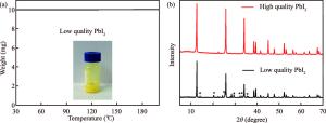
The CH3NH3PbI3 (MAPbI3) perovskite was usually prepared by high-purity PbI2 with high cost. The low cost and low-purity PbI2 was seldom reported for fabrication of MAPbI3 because it cannot even dissolve well in widely adopted solvent of DMF. We developed an easy method to adapt low-purity PbI2 for fabrication of high quality MAPbI3 just by the simple addition of some hydrochloric acid into the mixture of low-purity PbI2, MAI and DMF. This straightforward method can not only help dissolve the low quality PbI2 by reacting with some impurities in DMF, but also lead to a successful fabrication of high-quality perovskite solar cells with up to 14.80% efficiency comparable to the high quality PbI2 precursors.
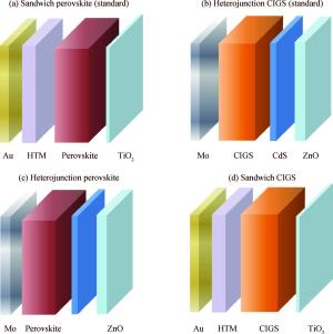
Heterojunction and sandwich architectures are two new-type structures with great potential for solar cells. Specifically, the heterojunction structure possesses the advantages of efficient charge separation but suffers from band offset and large interface recombination; the sandwich configuration is favorable for transferring carriers but requires complex fabrication process. Here, we have designed two thin-film polycrystalline solar cells with novel structures:sandwich CIGS and heterojunction perovskite, referring to the advantages of the architectures of sandwich perovskite (standard) and heterojunction CIGS (standard) solar cells, respectively. A reliable simulation software wxAMPS is used to investigate their inherent characteristics with variation of the thickness and doping density of absorber layer. The results reveal that sandwich CIGS solar cell is able to exhibit an optimized efficiency of 20.7%, which is much higher than the standard heterojunction CIGS structure (18.48%). The heterojunction perovskite solar cell can be more efficient employing thick and doped perovskite films (16.9%) than these typically utilizing thin and weak-doping/intrinsic perovskite films (9.6%). This concept of structure modulation proves to be useful and can be applicable for other solar cells.
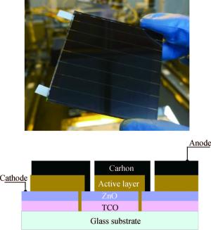
The recent dramatic rise in power conversion efficiencies (PCE) of perovskite solar cells has triggered intense research worldwide. However, their practical development is hampered by poor stability and low PCE values with large areas devices. Here, we developed a gas-pumping method to avoid pinholes and eliminate local structural defects over large areas of perovskite film, even for 5×5 cm2 modules, the PCE reached 10.6% and no significant degradation was found after 140 days of outdoor testing. Our approach enables the realization of high performance large-area PSCs for practical application.
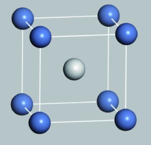
Using the first-principles plane-wave pseudo-potential method based on density functional theory, the effect of vacancy and anti-position defect on the mechanical and thermal properties of B2-NiSc intermetallics were discussed in detail. Several parameters, such as the shear modulus, bulk modulus, modulus of elasticity, C11-C12, the Debye temperature and Poisson's ratio, have been calculated to evaluate the effect of vacancy and anti-position defect on the hardness, ductility and thermal properties of B2-NiSc intermetallics. The results show that VNi, ScNi, VSc and NiSc the four point defects all make the crystal hardness decrease and improve plasticity of B2-NiSc intermetallics. The entropy, enthalpy and free energy of VNi, ScNi, VSc and NiSc are monotonously changed as temperature changes. From the perspective of free energy, NiSc is the most stable, while ScNi is the most unstable. Debye temperature of NiSc intermetallics with four different point defects shows VNi, ScNi, VSc and NiSc the four point defects all reduce the stability of B2-NiSc intermetallics.
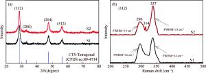
Ternary sphere-like Cu2SnS3(CTS) semiconductor and 2D hexagonal sheets were synthesized via a simple solvothermal method using PVP as the surface ligand at two temperatures of 180 and 220℃. The structural, morphological, and chemical compositions as well as optical properties of as-synthesized CTS particles were characterized using X-ray diffraction (XRD), Raman spectroscopy, energy dispersive X-ray spectrometry (EDS), field emission scanning electron microscopy (FESEM), and UV-Vis spectroscopy. The size of sphere-like particles and the side length of hexagonal sheets were within the range of 120-140 nm and 500 nm-2 μm, respectively. FESEM, XRD, and EDS were analyzed to investigate the mechanism of the morphological evolution of CTS particles. CTS particles showed proliferation of Sn atomic ratio, which is strongly sensitive to reaction temperature and, highly affects the increase of band gap energy from 1.36 to 1.53 eV due to generation metal defects and formation SnS2. The optical analysis via the transmittance and reflectance reveals that the band-gap energy of dropcasted CTS thin films decreases after annealing due to grain growth and change of chemical compositions. Photo-responses of CTS nanocrystal thin films indicated a considerable increase in the conductivity of the films under light illumination. All these results showed the potential of these films for solar cell applications.
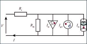
Electrical characterization analyses are proposed in this work using the Lambert function on Schottky junctions in GaN wide band gap semiconductor devices for extraction of physical parameters. The Lambert function is used to give an explicit expression of the current in the Schottky junction. This function is applied with defined conduction phenomena, whereas other work presented arbitrary (or undefined) conduction mechanisms in such parameters' extractions. Based upon AlGaN/GaN HEMT structures, extractions of parameters are undergone in order to provide physical characteristics. This work highlights a new expression of current with defined conduction phenomena in order to quantify the physical properties of Schottky contacts in AlGaN/GaN HEMT transistors.
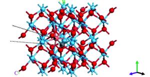
The physical mechanism of the resistance switching for RRAM with co-doped defects (Ag and oxygen vacancy) is studied based on the first principle calculations and the simulation tool VASP. The interaction energy, formation energy and density of states of Ag and oxygen vacancy defect (VO) are calculated. The calculated results reveal that the co-doped system is more stable than the system only doped either Ag or VO defect and the impurity energy levels in the band gap are contributed by Ag and VO defects. The obtained partial charge density confirmed further that the clusters are obvious in the direction of Ag to Hf ions, which means that it is Ag but VO plays a role of conductive paths. For the formation mechanism, the modified electron affinity and the partial charge density difference are calculated. The results show that the ability of electron donors of Ag is stronger than Vm O In conclusion, the conductivity of the physical mechanism of resistance switching in the co-doped system mainly depends on the doped Ag.
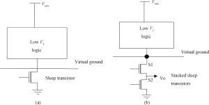
In this paper we have investigated the single phase sleep signal modulation technique, step-wise Vgs technique and the three-phase reactivation technique to evaluate the noise characteristics of multi-threshold CMOS circuits used in communication systems. The stacking technique is also implemented in this paper for the sleep transistor. The stacking approach helps to minimize leakage power. The mode transition noise minimization techniques have been applied to 32-bit dynamic TSPC adder with stacked sleep transistors in a standard 45-nm CMOS process. The reactivation noise, delay and energy consumption of all the three techniques have been evaluated. It has been shown that the three phase modulation technique significantly minimizes the reactivation delay when the peak noise level is maintained the same for all three techniques. The three phase modulation technique shows 67.3% and 35% reduction in delay compared to the single phase and step-wise Vgs modulation techniques respectively. The reactivation energy is also suppressed by 49.3% and 39.14% with respect to the single-phase and stepwise Vgs techniques.


