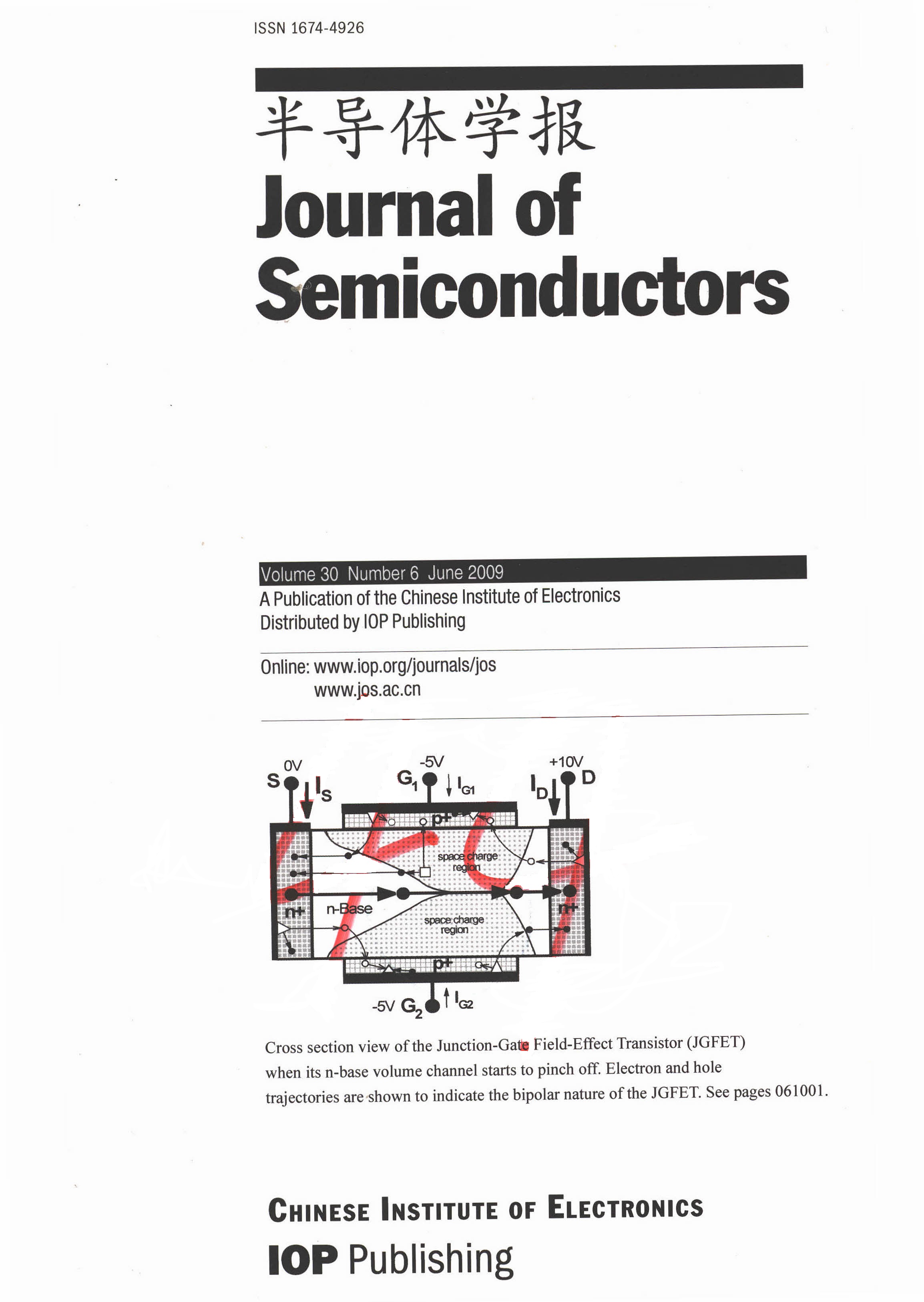
This paper describes the definition of the complete transistor. For semiconductor devices, the complete transistor is always bipolar, namely, its electrical characteristics contain both electron and hole currents controlled by their spatial charge distributions. Partially complete or incomplete transistors, via coined names or/and designed physical geometries, included the 1949 Shockley p/n junction transistor (later called Bipolar Junction Transistor, BJT), the 1952 Shockley unipolar ‘field-effect’ transistor (FET, later called the p/n Junction Gate FET or JGFET), as well as the field-effect transistors introduced by later investigators. Similarities between the surface-channel MOS-gate FET (MOSFET) and the volume-channel BJT are illustrated. The bipolar currents, identifed by us in a recent nanometer FET with 2-MOS-gates on thin and nearly pure silicon base, led us to the recognition of the physical makeup and electrical current and charge compositions of a complete transistor and its extension to other three or more terminal signal processing devices, and also the importance of the terminal contacts.
Spin splitting of conduction subbands in Al0.3Ga0.7As/GaAs/AlxGa1-xAs/Al0.3Ga0.7As step quantum wells induced by interface and electric field related Rashba effects is investigated theoretically by the method of finite difference. The dependence of the spin splitting on the electric field and the well structure, which is controlled by the well width and the step width, is investigated in detail. Without an external electric field, the spin splitting is induced by an interface related Rashba term due to the built-in structure inversion asymmetry. Applying the external electric field to the step QW, the Rashba effect can be enhanced or weakened, depending on the well structure as well as the direction and the magnitude of the electric field. The spin splitting is mainly controlled by the interface related Rashba term under a negative and a stronger positive electric field, and the contribution of the electric field related Rashba term dominates in a small range of a weaker positive electric field. A method to determine the interface parameter is proposed. The results show that the step QWs might be used as spin switches.
The variational method and the effective mass approximation are used to calculate the phonon effects on the hydrogenic impurity states in a cylindrical quantum wire with finite deep potential by taking both the couplings of the electron-confined bulk longitudinal optical (LO) phonons and the impurity-ion–LO phonons into account. The binding energies and the phonon contributions are calculated as functions of the transverse dimension of the quantum wire. The results show that the polaronic effect induced by the electron–LO phonon coupling and the screening effect induced by the impurity-ion–LO phonon coupling tend to compensate each other and the total effects reduce the impurity binding energies.
Molecular dynamics simulations with Stillinger–Weber potential are used to study the tensile and melting behavior of single-crystalline silicon nanowires (SiNWs). The tensile tests show that the tensile behavior of the SiNWs is strongly dependent on the simulation temperature, the strain rate, and the diameter of the nanowires. For a given diameter, the critical load significantly decreases as the temperature increases and also as the strain rate decreases. Additionally, the critical load increases as the diameter increases. Moreover, the melting tests demonstrate that both melting temperature and melting heat of the SiNWs decrease with decreasing diameter and length, due to the increase in surface energy. The melting process of SiNWs with increasing temperature is also investigated.
Boron-doped hydrogenated silicon films with different gaseous doping ratios (B2H6/SiH4) were deposited in a plasma-enhanced chemical vapor deposition (PECVD) system. The microstructure of the films was investigated by atomic force microscopy (AFM) and Raman scattering spectroscopy. The electrical properties of the films were characterized by their room temperature electrical conductivity (σ) and the activation energy (Ea). The results show that with an increasing gaseous doping ratio, the silicon films transfer from a microcrystalline to an amorphous phase, and corresponding changes in the electrical properties were observed. The thin boron-doped silicon layers were fabricated as recombination layers in tunnel junctions. The measurements of the I–V characteristics and the transparency spectra of the junctions indicate that the best gaseous doping ratio of the recombination layer is 0.04, and the film deposited under that condition is amorphous silicon with a small amount of crystallites embedded in it. The junction with such a recombination layer has a small resistance, a nearly ohmic contact, and a negligible optical absorption.
The optical properties of porous silicon (PS) samples fabricated by pulse etching in a temperature range from -40 to 50 ℃ have been investigated using reflectance spectroscopy, photoluminescence spectroscopy, and scanning electron microscopy (SEM). The dependence of the optical parameters, such as the refractive index n and the optical thickness (nd) of PS samples, on the etching temperature has been analyzed in detail. As the etching temperature decreases, n decreases, indicating a higher porosity, and the physical thickness of PS samples also decreases. Meanwhile, the reflectance spectra exhibit a more intense interference band and the interfaces are smoother. In addition, the intensity of the PL emission spectra is dramatically increased.
The Si2Sb2Te5 phase change material has been studied by applying a nano-tip (30 nm in diameter) on an atomic force microscopy system. Memory switching from a high resistance state to a low resistance state has been achieved, with a resistance change of about 1000 times. In a typical I–V curve, the current increases significantly after the voltage exceeds ~4.3 V. The phase transformation of a Si2Sb2Te5 film was studied in situ by means of in situ X-ray diffraction and temperature dependent resistance measurements. The thermal stability of Si2Sb2Te5 and Ge2Sb2Te5 was characterized and compared as well.
Using a low temperature hydrothermal synthesis method, ZnO nanorod networks have been directly grown across trenched Au microelectrodes arrays, which were modified with a layer of ZnO seeds. The characteristics of the current–voltage (I–V) and the photo response were obtained both in the dark and under ultraviolet illumination. The bridged nanorod network demonstrated a highly sensitive response to UV illumination in atmosphere at room temperature. It can be useful for nanoscale optoelectronic applications, serving as chemical sensors, biological sensors, and switching devices.
A P+-nc-Si:H film (boron-doped nc-Si:H thin film) was used as a complex anode of an OLED. As an ideal candidate for the composite anode, the P+-nc-Si:H thin film has a good conductivity with a high work function (~5.7 eV) and outstanding optical properties of high reflectivity, transmission, and a very low absorption. As a result, the combination of the relatively high reflectivity of a P+-nc-Si:H film/ITO complex anode with the very high reflectivity of an Al cathode could form a micro-cavity structure with a certain Q to improve the efficiency of the OLED fabricated on it. An RGB pixel generated by microcavity OLEDs is beneficial for both the reduction of the light loss and the improvement of the color purity and the efficiency. The small molecule Alq would be useful for the emitting light layer (EML) of the MOLED, and the P+-nc-Si film would be used as a complex anode of the MOLED, whose configuration can be constructed as Glass/LTO/P+-nc-Si:H/ITO/MoO3/NPB/Alq/LiF/Al. By adjusting the thickness of the organic layer NPB/Alq, the optical length of the microcavity and the REB colors of the device can be obtained. The peak wavelengths of an OLED are located at 486, 550, and 608 nm, respectively. The CIE coordinates are (0.21, 0.45), (0.33, 0.63), and (0.54, 0.54), and the full widths at half maximum (FWHM) are 35, 32, and 39 nm for red, green, and blue, respectively.
We have fabricated In0.53Ga0.47As/AlAs/InP resonant tunneling diodes (RTDs) based on the air-bridge technology by using electron beam lithography processing. The epitaxial layers of the RTD were grown on semi-insulating (100) InP substrates by molecular beam epitaxy. RTDs with a peak current density of 24.6 kA/cm2 and a peak-to-valley current ratio of 8.6 at room temperature have been demonstrated.
A novel device structure with a vertical double-gate and dual-strained channel is presented. The electri-cal characteristics of this device with a gate length of 100 nm are simulated. With a Ge content of 20%, the drain currents of the strained-Si NMOSFET and the strained-SiGe PMOSFET compared to the universal SOI MOSFETs are enhanced by 26% and 33%, respectively; the risetime and the falltime of the strained-channel CMOS are greatly decreased by 50% and 25.47% compared to their traditional Si channel counterparts. The simulation results show that the vertical double-gate (DG) dual-strained-channel MOSFETs exhibit better drive capability, a higher transcon-ductance, and a faster circuit speed for CMOS compared to conventional-Si MOSFETs. The new structure can be achieved by today's semiconductor manufacturing level.
Under a large signal drive level, a frequency domain black box model of the nonlinear scattering function is introduced into power FETs and diodes. A time domain measurement system and a calibration method based on a digital oscilloscope are designed to extract the nonlinear scattering function of semiconductor devices. The extracted models can reflect the real electrical performance of semiconductor devices and propose a new large-signal model to the design of microwave semiconductor circuits.
Three aging experiments were performed for AlGaInP light emitting diodes (LED) with or without indium tin oxide (ITO), which is used as a current spreading layer. It was found that the voltage of the LED with an ITO film increased at a high current stressing, while there was little change for that of the LED without the ITO. The results of the LEDs with different thicknesses of the ITO film show that the LED with a thicker ITO has a higher reliability. The main reason for the voltage increase of the LED with the ITO film might be the current crowding in the ITO film around the P-type electrode.
A novel asymmetric broad waveguide diode laser structure was designed for high power conversion efficiency (PCE). The internal quantum efficiency, the series resistance, and the thermal resistance were theoretically optimized. The series resistance and the thermal resistance were greatly decreased by optimizing the thickness of the P-waveguide and the P-cladding layers. The internal quantum efficiency was increased by introducing a novel strain-compensated GaAs0.9P0.1/InGaAs quantum well. Experimentally, a single 1-cm bar with 20% fill factor and 900 μm cavity length was mounted P-side down on a microchannel-cooled heatsink, and a peak PCE of 60% is obtained at 26.3-W continuous wave output power. The results prove that this novel asymmetric waveguide structure design is an efficient approach to improve the PCE.
In order to investigate the effects of a back surface field (BSF) on the performance of a p-doped amor-phous silicon (p-a-Si:H)/n-doped crystalline silicon (n-c-Si) solar cell, a heterojunction solar cell with a p-a-Si:H/n-c-Si/n+-a-Si:H structure was designed. An n+-a-Si:H film was deposited on the back of an n-c-Si wafer as the BSF. The photovoltaic performance of p-a-Si:H/n-c-Si/n+-a-Si:H solar cells were simulated. It was shown that the BSF of the p-a-Si:H/n-c-Si/n+-a-Si:H solar cells could effectively inhibit the decrease of the cell performance caused by interface states.
A silicon (SiNW) nanowire device, made by the bottom-up method, has been assembled in a MEMS device for measuring stress in cantilevers. The process for assembling a SiNW on a cantilever has been introduced. The current as a function of the voltage applied to a SiNW have been measured, and the different resistances before and after cantilever releasing have been observed. A parameter, , has been derived based on the resistances. For a fixed sample, a linear relationship between and the stress in the cantilever has been observed; and, so, it has been demonstrated that the resistance of SiNW can reflect the variation of the cantilever stress.
The influence of electron irradiation on the switching speed in insulated gate bipolar transistors (IGBT) with different epitaxial layer thicknesses is discussed in detail. The experimental results prove that the fall time of IGBT increases when increasing the thickness of the epitaxial layer. However, there is no obvious difference between the ratios of the fall time after irradiation to those before irradiation for different epitaxial layer thicknesses. The increase in switching speed of the IGBT is accompanied by an increase in the forward drop, and a trade-off curve between forward voltage drop and fall time of IGBT is presented.
This paper introduces major characteristics of the single event latchup (SEL) in CMOS devices. We accomplish SEL tests for CPU and SRAM devices through the simulation by a pulse laser. The laser simulation results give the energy threshold for samples to undergo SEL. SEL current pulses are measured for CMOS devices in the latchup state, the sensitive areas in the devices are acquired, the major traits, causing large scale circuits to undergo SEL, are summarized, and the test equivalence between a pulse laser and ions is also analyzed.
One challenge of the implementation of fully-integrated RF power amplifiers into a deep submicro digital CMOS process is that no capacitor is available, especially no high density capacitor. To address this problem, a two-stage class-AB power amplifier with inter-stage matching realized by an inter-metal coupling capacitor is designed in a 180-nm digital CMOS process. This paper compares three structures of inter-metal coupling capacitors with metal-insulator-metal (MIM) capacitor regarding their capacitor density. Detailed simulations are carried out for the leakage, the voltage dependency, the temperature dependency, and the quality factor between an inter-metal shuffled (IMS) capacitor and an MIM capacitor. Finally, an IMS capacitor is chosen to perform the inter-stage matching. The techniques are validated via the design and implement of a two-stage class-AB RF power amplifier for an UHF RFID application. The PA occupies 370×200 μm2 without pads in the 180-nm digital CMOS process and outputs 21.1 dBm with 40% drain efficiency and 28.1 dB power gain at 915 MHz from a single 3.3 V power supply.
This paper presents a pipelined current mode analog to digital converter (ADC) designed in a 0.5-μm CMOS process. Adopting the global and local bias scheme, the number of interconnect signal lines is reduced numerously, and the ADC exhibits the advantages of scalability and portability. Without using linear capacitance, this ADC can be implemented in a standard digital CMOS process; thus, it is suitable for applications in the system on one chip (SoC) design as an analogue IP. Simulations show that the proposed current mode ADC can operate in a wide supply range from 3 to 7 V and a wide quantization range from ±64 to ±256 μA. Adopting the histogram testing method, the ADC was tested in a 3.3 V supply voltage/±64 A quantization range and a 5 V supply voltage/±256 μA quantization range, respectively. The results reveal that this ADC achieves a spurious free dynamic range of 61.46 dB, DNL/INL are –0.005 to +0.027 LSB/–0.1 to +0.2 LSB, respectively, under a 5 V supply voltage with a digital error correction technique.
The design, implementation, and characterization of an image-rejection double quadrature conversion mixer based on RC asymmetric polyphase filters (PPF) are presented. The mixer consists of three sets of PPFs and a mixer core for quadrature down conversion. Two sets of PPFs are used for the quadrature generation and the other one is used for the IF signal selection to reject the unwanted image band. Realized in 0.18-μm CMOS technology as a part of the DVB-T receiver chip, the mixer exhibits a high image rejection ratio (IRR) of 58 dB, a power consumption of 11 mW, and a 1-dB gain compression point of –15 dBm.
Digital calibration and control techniques for narrow band integrated low-IF receivers with on-chip frequency synthesizer are presented. The calibration and control system, which is adopted to ensure an achievable signal-to-noise ratio and bit error rate, consists of a digitally controlled, high resolution dB-linear automatic gain control (AGC), an inphase (I) and quadrature (Q) gain and phase mismatch calibration, and an automatic frequency calibration (AFC) of a wideband voltage-controlled oscillator in a PLL based frequency synthesizer. The calibration system has a low design complexity with little power and small die area. Simulation results show that the calibration system can enlarge the dynamic range to 72 dB and minimize the phase and amplitude imbalance between I and Q to 0.08° and 0.024 dB, respectively, which means the image rejection ratio is better than 60 dB. In addition, the calibration time of the AFC is 1.12 μs only with a reference clock of 100 MHz.
A novel technique using a keeper with a simultaneous low supply voltage and low body voltage is proposed to improve the overall performance of high fan-in OR gates without modifying the physical dimensions of the keeper. Simulation results of a 16-input domino OR gate using 45 nm CMOS technology show that the proposed technique could trade off between a high power/speed efficient operation and the robustness to noise effectively. Also, a Monte Carlo analysis indicates that the proposed domino OR gate is more robust to parameter variation compared to a conventional domino OR gate.
A CMOS variable gain amplifier (VGA) that adopts a novel exponential gain approximation is presented. No additional exponential gain control circuit is required in the proposed VGA used in a direct conversion receiver. A wide gain control voltage from 0.4 to 1.8 V and a high linearity performance are achieved. The three-stage VGA with automatic gain control (AGC) and DC offset cancellation (DCOC) is fabricated in a 0.18-μm CMOS technology and shows a linear gain range of more than 58-dB with a linearity error less than 1 dB. The 3-dB bandwidth is over 8 MHz at all gain settings. The measured input-referred third intercept point (IIP3) of the proposed VGA varies from –18.1 to 13.5 dBm, and the measured noise figure varies from 27 to 65 dB at a frequency of 1 MHz. The dynamic range of the closed-loop AGC exceeds 56 dB, where the output signal-to-noise-and-distortion ratio (SNDR) reaches 20 dB. The whole circuit, occupying 0.3 mm2 of chip area, dissipates less than 3.7 mA from a 1.8-V supply.
An analog baseband circuit made in a 0.35-μm SiGe BiCMOS process is presented for China Multi-media Mobile Broadcasting (CMMB) direct conversion receivers. A high linearity 8th-order Chebyshev low pass filter (LPF) with accurate calibration system is used. Measurement results show that the filter provides 0.5-dB pass-band ripple, 4% bandwidth accuracy, and –35-dB attenuation at 6 MHz with a cutoff frequency of 4 MHz. The current steering type variable gain amplifier (VGA) achieves more than 40-dB gain range with excellent temperature compensation. This tuner baseband achieves an OIP3 of 25.5 dBm, dissipates 16.4 mA under a 2.8-V supply and occupies 1.1 mm2 of die size.
To implement a fully-integrated on-chip CMOS power amplifier (PA) for RFID readers, the resonant frequency of each matching network is derived in detail. The highlight of the design is the adoption of a bonding wire as the output-stage inductor. Compared with the on-chip inductors in a CMOS process, the merit of the bondwire inductor is its high quality factor, leading to a higher output power and efficiency. The disadvantage of the bondwire inductor is that it is hard to control. A highly integrated class-E PA is implemented with 0.18-μm CMOS process. It can provide a maximum output power of 20 dBm and a 1 dB output power of 14.5 dBm. The maximum power-added efficiency (PAE) is 32.1%. Also, the spectral performance of the PA is analyzed for the specified RFID protocol.
A novel cascaded charge-sharing technique is presented in content-addressable memories (CAMs), which not only effectively reduces the match-line (ML) power by using a pre-select circuit, but also realizes a high search speed. Pre-layout simulation results show a 75.9% energy-delay-product (EDP) reduction of the MLs over the tradi-tional precharge-high ML scheme and 41.3% over the segmented ML method. Based on this technique, a test-chip of 64-word×144-bit ternary CAM (TCAM) is implemented using a 0.18-μm 1.8-V CMOS process, achieving an 1.0 ns search delay and 4.81 fJ/bit/search for the MLs.
This paper presents a universal field programmable gate array (FPGA) programmable routing circuit, focusing primarily on a delay optimization. Under the precondition of the routing resource's flexibility and routabil-ity, the number of programmable interconnect points (PIP) is reduced, and a multiplexer (MUX) plus a BUFFER structure is adopted as the programmable switch. Also, the method of offset lines and the method of complementary hanged end-lines are applied to the TILE routing circuit and the I/O routing circuit, respectively. All of the above features ensure that the whole FPGA chip is highly repeatable, and the signal delay is uniform and predictable over the total chip. Meanwhile, the BUFFER driver is optimized to decrease the signal delay by up to 5%. The proposed routing circuit is applied to the Fudan programmable device (FDP) FPGA, which has been taped out with an SMIC 0.18-μm logic 1P6M process. The test result shows that the programmable routing resource works correctly, and the signal delay over the chip is highly uniform and predictable.
We developed a simplified nanofabrication process for imprint templates by fast speed electron beam lithography (EBL) and a dry etch technique on a SiNx substrate, intended for large area manufacturing. To this end, the highly sensitive chemically amplified resist (CAR), NEB-22, with negative tone was used. The EBL process first defines the template pattern in NEB-22, which is then directly used as an etching mask in the subsequent reactive ion etching (RIE) on the SiNx to form the desired templates. The properties of both e-beam lithography and dry etch of NEB-22 were carefully studied, indicating significant advantages of this process with some drawbacks compared to when Cr was used as an etching mask. Nevertheless, our results open up a good opportunity to fabricate high resolution imprint templates with the prospect of wafer scale manufacturing.
For thick resist implant layers, such as a high voltage P well and a deep N well, systematic and uncor-rectable overlay residues brought about by the tapered resist profiles were found. It was found that the tapered profile is closely related to the pattern density. Potential solutions of the manufacturing problem include hardening the film solidness or balancing the exposure density. In this paper, instead of focusing on the process change methodology, we intend to solve the issue of the overlay metrology error from the perspective of the overlay mark design. Based on the comparison of the overlay performances between the proposed overlay mark and the original design, it is shown that the optimized overlay mark target achieves better performance in terms of profiles, dynamic precision, tool induced shift (TIS), and residues. Furthermore, five types of overlay marks with dummy bars are studied, and a recommendation for the overlay marks is given.