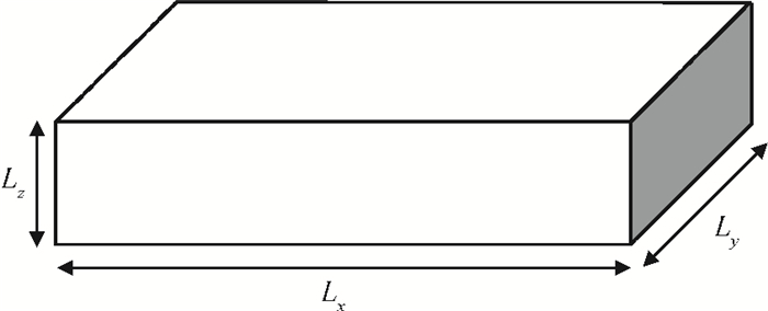
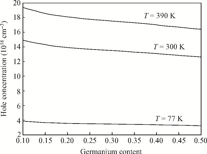
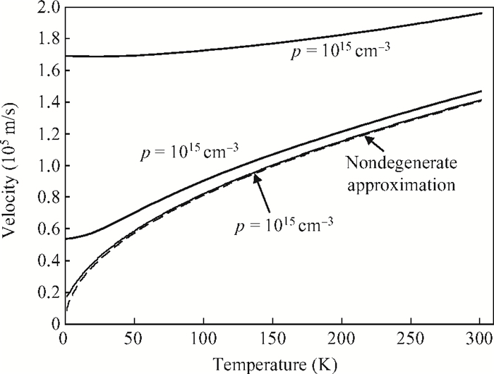
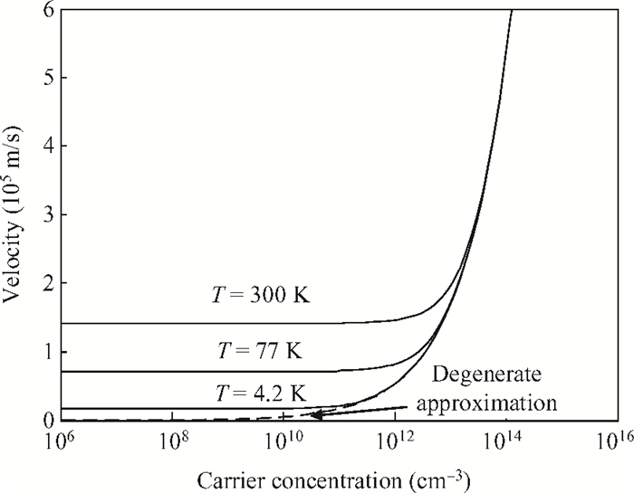
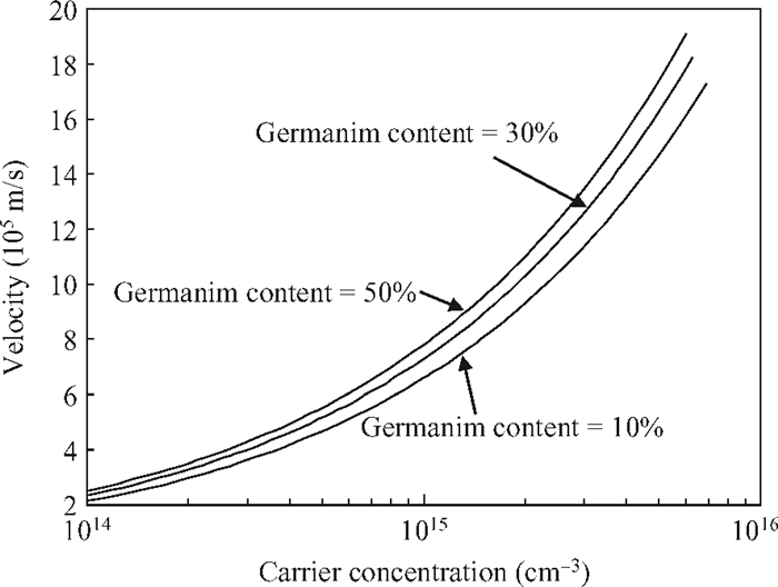
The impact of the fraction of germanium on the carrier performance of two-dimensional strained silicon, which embraces both the non-degenerate and degenerate regimes, is developed. In this model, the Fermi integral of order zero is employed. The impact of the fraction of germanium on the relaxed Si1-xGex substrate (x), carrier concentration and temperature is reported. It is revealed that the effect of x on the hole concentration is dominant for a normalized Fermi energy of more than three, or in other words the non-degenerate regime. On the contrary, the x gradient has less influence in the degenerate regime. Furthermore, by increasing x there is an increase in the intrinsic velocity, particularly with high carrier concentration and temperature.


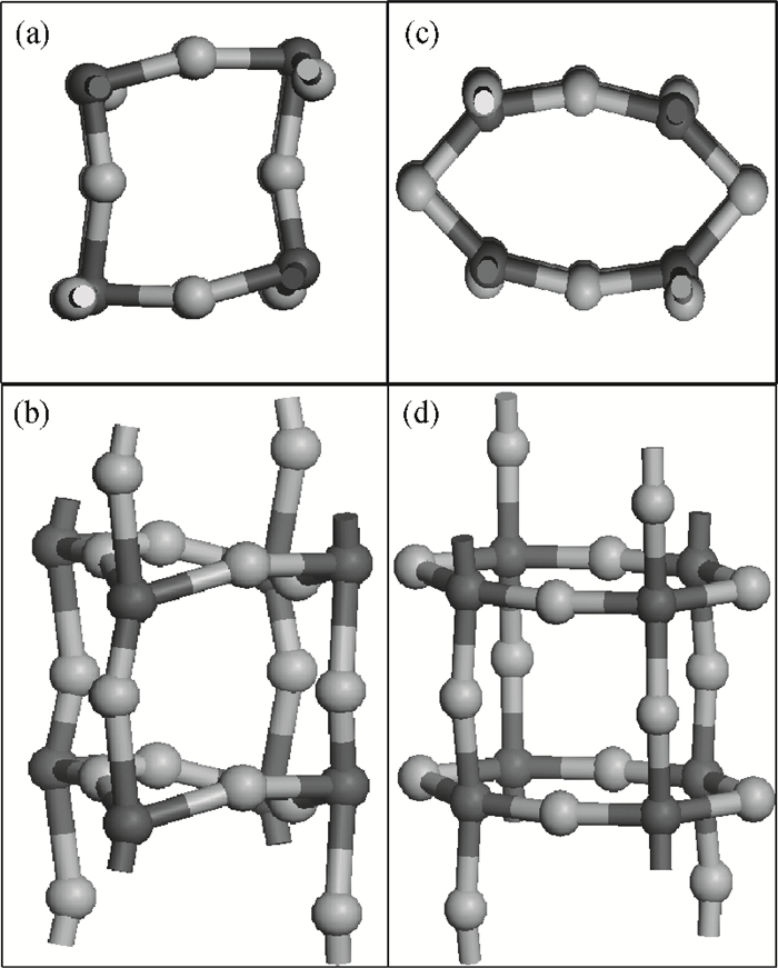
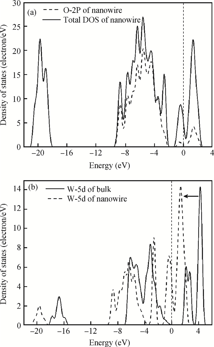
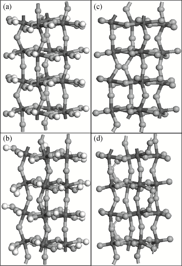
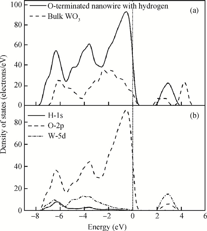
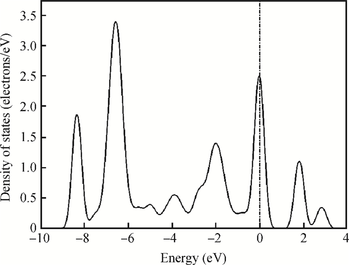
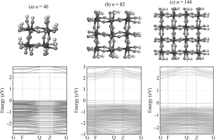
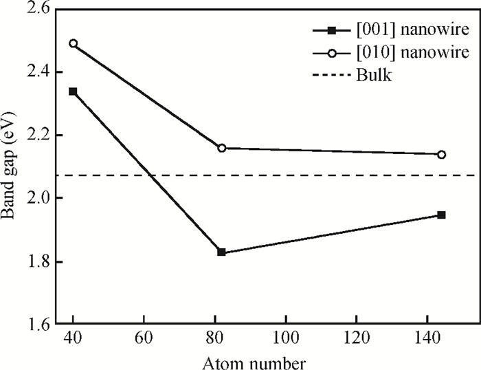
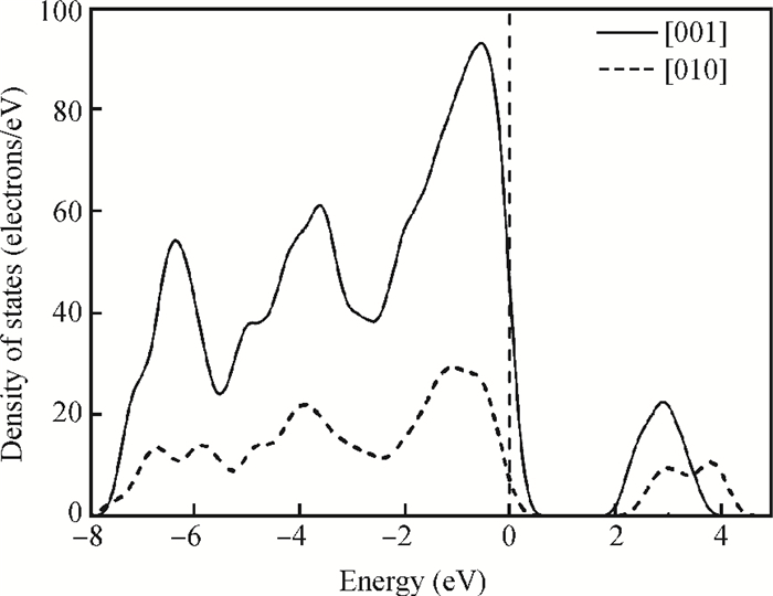
The effects of the surface and orientation of a WO3 nanowire on the electronic structure are investigated by using first principles calculation based on density functional theory (DFT). The surface of the WO3 nanowire was terminated by a bare or hydrogenated oxygen monolayer or bare WO2 plane, and the[010]-and[001]-oriented nanowires with different sizes were introduced into the theoretical calculation to further study the dependence of electronic band structure on the wire size and orientation. The calculated results reveal that the surface structure, wire size and orientation have significant effects on the electronic band structure, bandgap, and density of states (DOS) of the WO3 nanowire. The optimized WO3 nanowire with different surface structures showed a markedly dissimilar band structure due to the different electronic states near the Fermi level, and the O-terminated[001] WO3 nanowire with hydrogenation can exhibit a reasonable indirect bandgap of 2.340 eV due to the quantum confinement effect, which is 0.257 eV wider than bulk WO3. Besides, the bandgap change is also related to the orientation-resulted surface reconstructed structure as well as wire size.

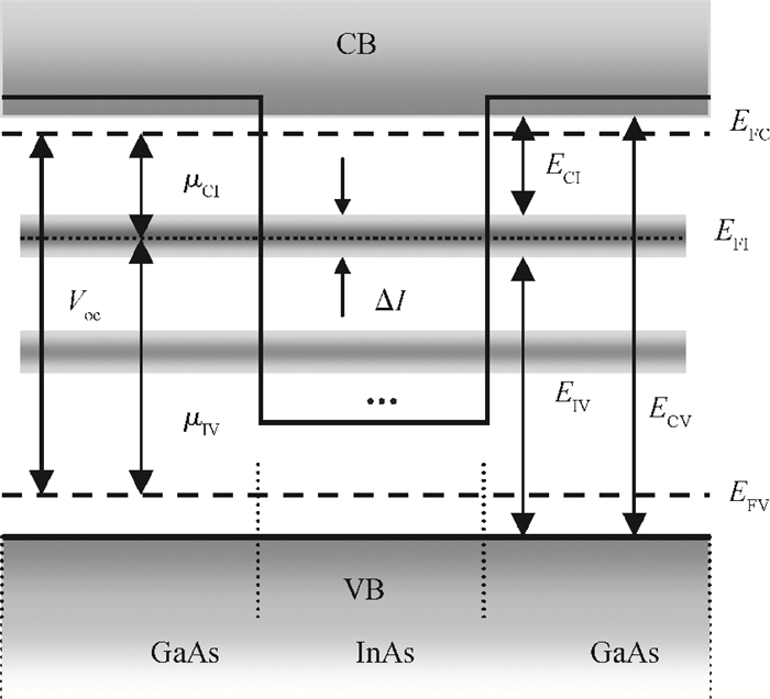
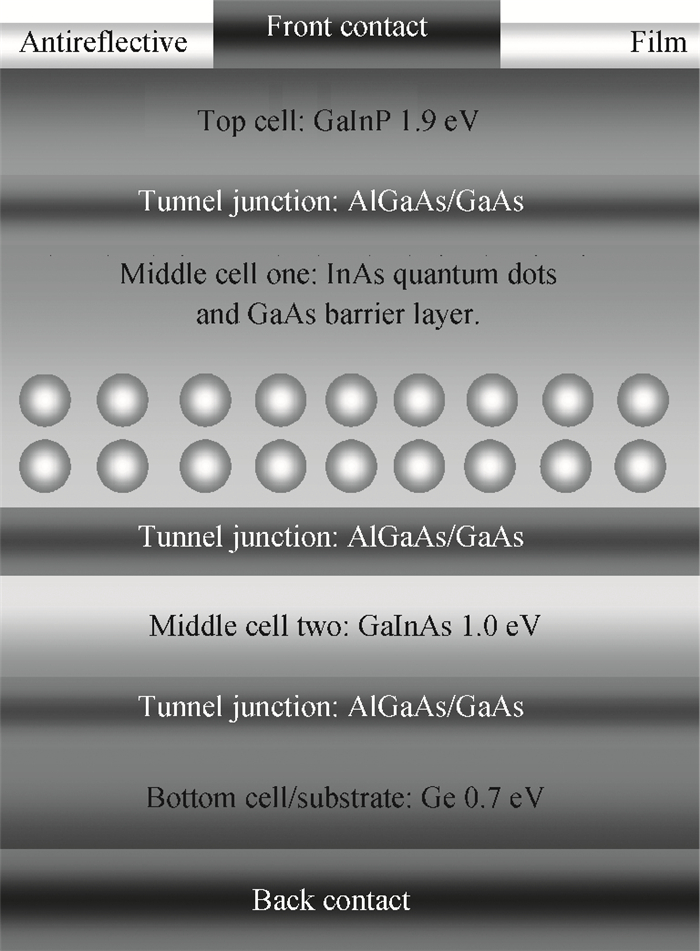
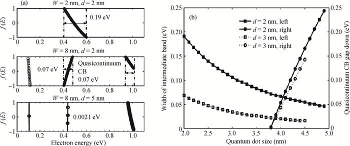
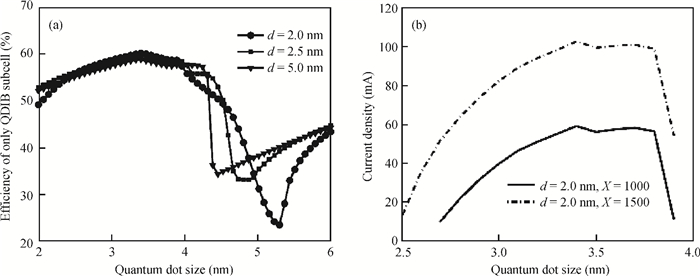
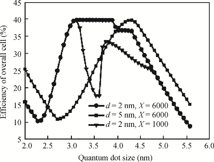
A metamorphic GaInP/GaAs/GaInAs/Ge multi-junction solar cell with InAs quantum dots is investigated, and the analytical expression of the energy conversion efficiency on the multi-junction tandem solar cell is derived using the detailed balance principle and the Kronig-Penney model. The influences of interdot distance, quantum-dot size and the intermediate band location on the energy conversion efficiency are studied. This shows that the maximum efficiency, as a function of quantum-dot size and distance, is about 60.15% under the maximum concentration for only one InAs/GaAs subcell, and is even up to 39.69% for the overall cell. In addition, other efficiency factors such as current mismatch, the formation of a quasicontinuum conduction band and concentrated light are examined.
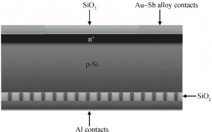
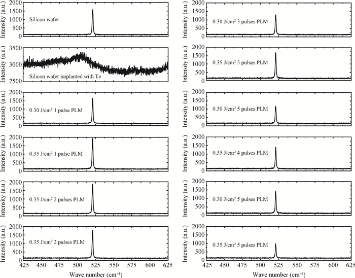
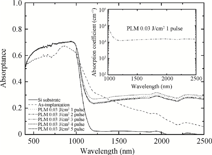
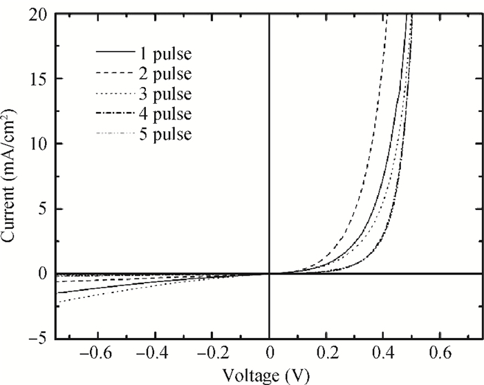
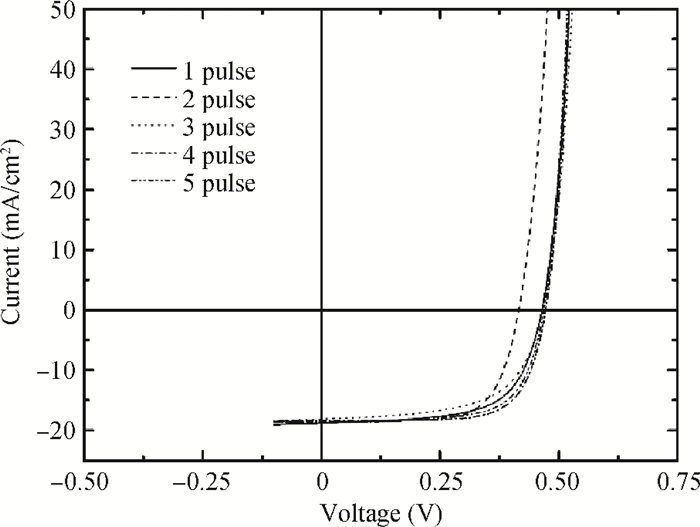
Pn junctions based on single crystalline tellurium supersaturated silicon were formed by ion implantation followed by pulsed laser melting (PLM). P type silicon wafers were implanted with 245 keV 126Te+ to a dose of 2×10¹⁵ ions/cm2, after a PLM process (248 nm, laser fluence of 0.30 and 0.35 J/cm2, 1-5 pulses, duration 30 ns), an n+ type single crystalline tellurium supersaturated silicon layer with high carrier density (highest concentration 4.10×1019 cm-3, three orders of magnitude larger than the solid solution limit) was formed, it shows high broadband optical absorption from 400 to 2500 nm. Current-voltage measurements were performed on these diodes under dark and one standard sun (AM 1.5), and good rectification characteristics were observed. For present results, the samples with 4-5 pulses PLM are best.
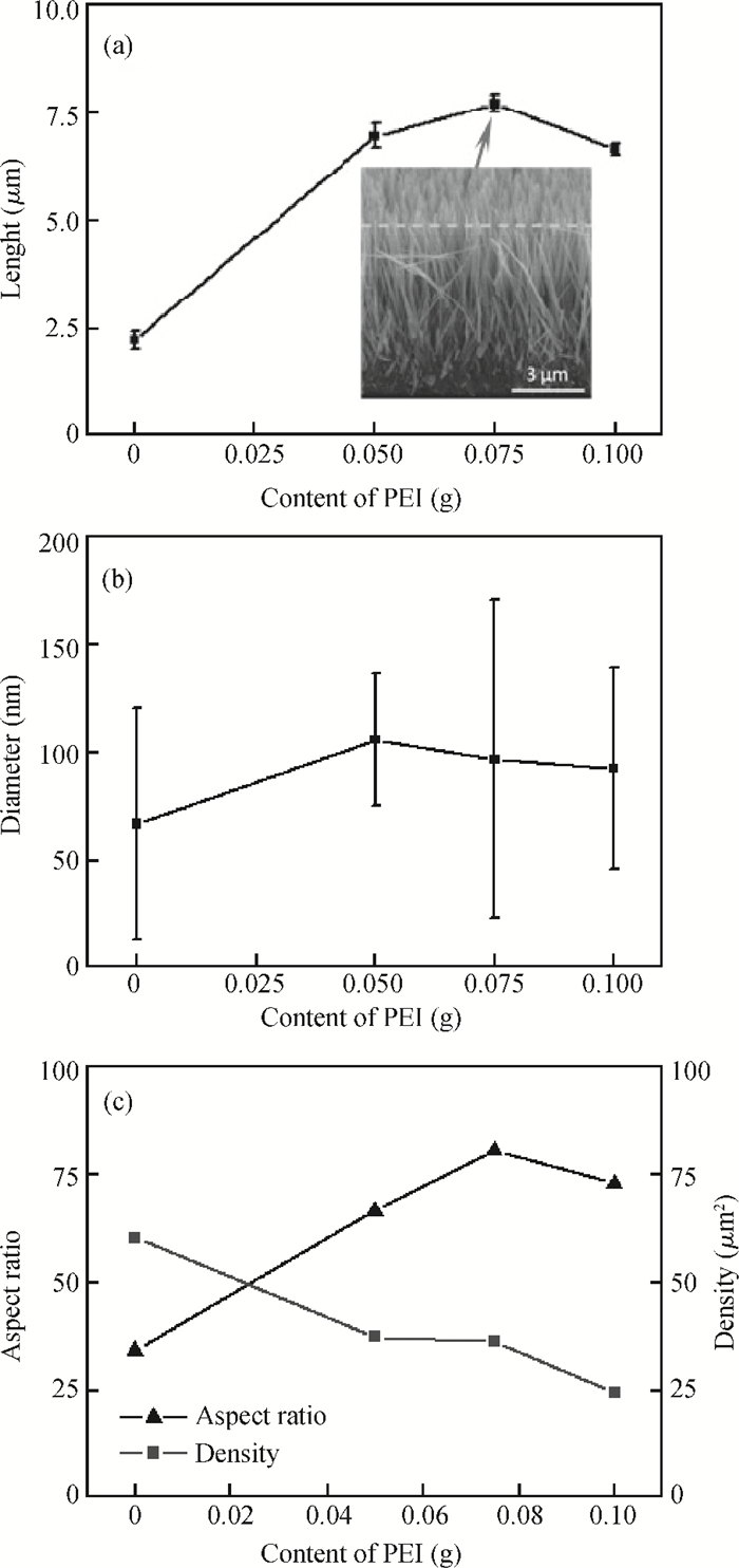
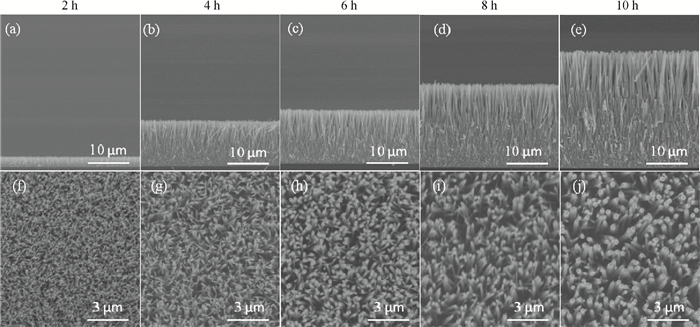
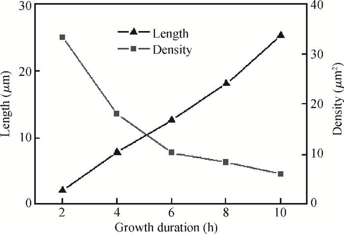
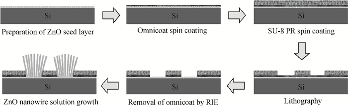
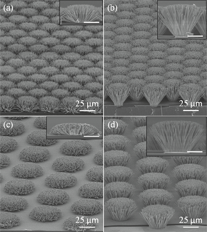
Well-aligned ZnO nanowires were hydrothermally synthesized based on a facile method for preparing the ZnO seed layer which was derived from the combination of a sol-gel process and the spin-coating technique. The effect of the contents of growth solution and the growth duration on the morphology of ZnO nanowires has been investigated. The results indicated that long and vertically aligned ZnO nanowires could be obtained by adjusting the contents of ammonia and polyethyleneimine (PEI) in the growth solution. Under the optimized condition, the length of ZnO nanowires increased fast and almost linearly with the growth duration. After 10 h incubation, ZnO nanowires more than 25 μm in length were obtained. By combining the conventional photolithographic method with this hydrothermal approach, long and well-aligned ZnO nanowire arrays were selectively grown on the substrate. In addition, the bottom fusion at the foot of the nanowires has been obviously improved. The results demonstrated that the improved hydrothermal process is favorable to synthesize long and well-aligned ZnO nanowires, and possesses good process compatibility with the conventional photolithographic technique for preparing ZnO nanowire arrays. So it has great potential in applications such as display and field emission devices.


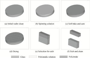
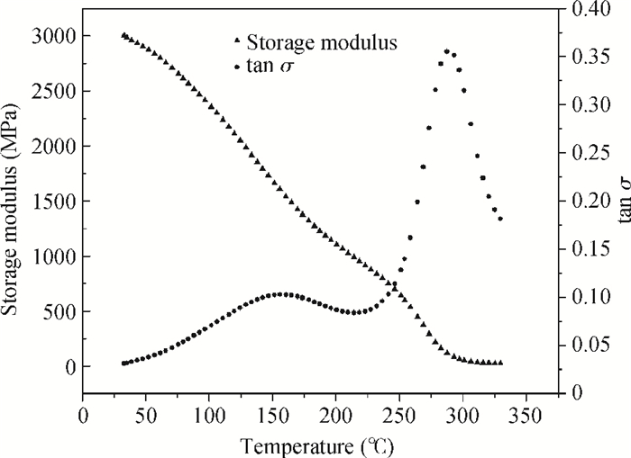
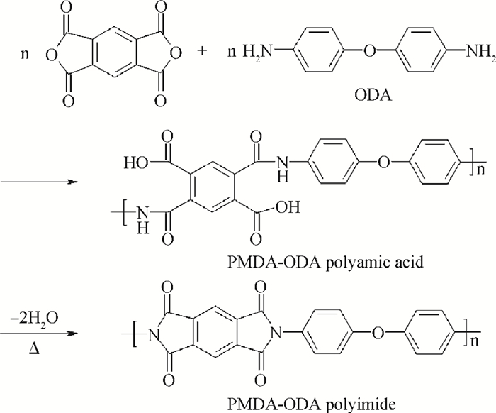
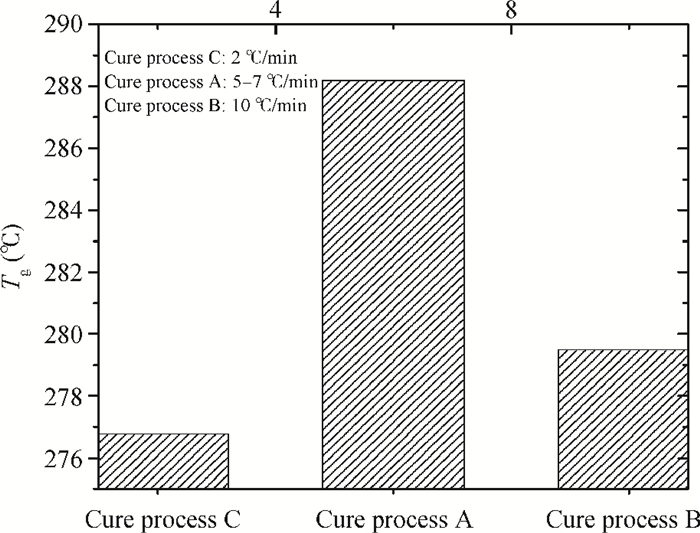
The effects of cure temperature history on the stability of hinged structure poly (4, 4-oxydiphenylene pyromellitimide) (PMDA-ODA) polyimide were studied by dynamic mechanical analysis. The polyimide films were cured under different curing conditions and peeled off by substrate etching. It was found that a proper cure time and temperature ramp rate improves the stability in terms of higher glass transition temperature. Ninety minutes at 375℃ or 200℃ is a beneficial high glass transition temperature. The temperature ramp rate should be between 2℃/min and 10℃/min, which is neither too high nor too low.

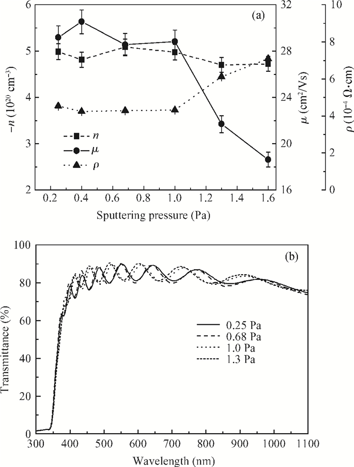
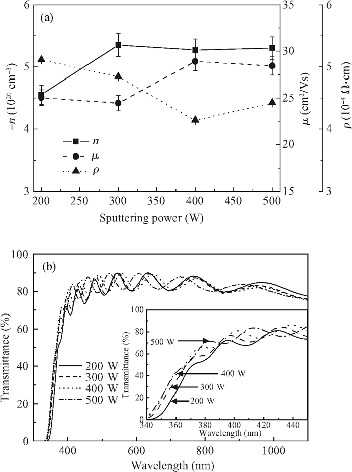
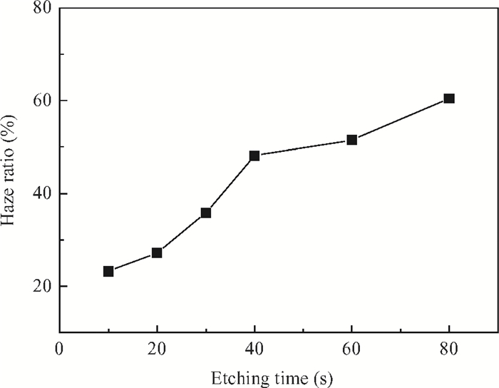
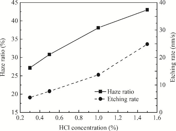
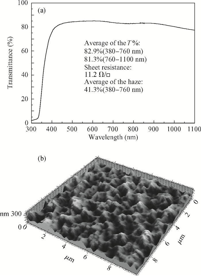
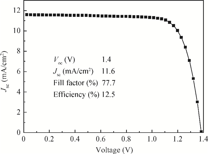
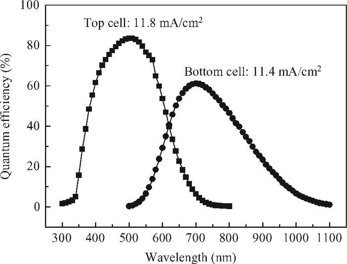
This study deals with the optimization of direct current (DC) sputtered aluminum-doped zinc oxide (AZO) thin films and their incorporation into a-Si:H/μc-Si:H tandem junction thin film solar cells aiming for high conversion efficiency. Electrical and optical properties of AZO films, i.e. mobility, carrier density, resistivity, and transmittance, were comprehensively characterized and analyzed by varying sputtering deposition conditions, including chamber pressure, substrate temperature, and sputtering power. The correlations between sputtering processes and AZO thin film properties were first investigated. Then, the AZO films were textured by diluted hydrochloric acid wet etching. Through optimization of deposition and texturing processes, AZO films yield excellent electrical and optical properties with a high transmittance above 81% over the 380-1100 nm wavelength range, low sheet resistance of 11 Ω/$\square$ and high haze ratio of 41.3%. In preliminary experiments, the AZO films were applied to a-Si:H/μc-Si:H tandem thin film solar cells as front contact electrodes, resulting in an initial conversion efficiency of 12.5% with good current matching between subcells.


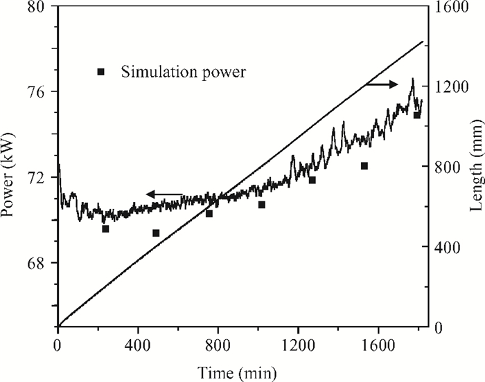
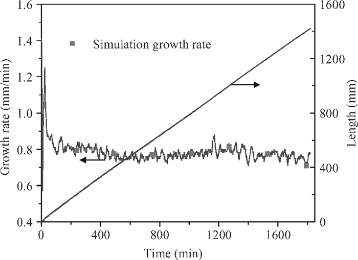
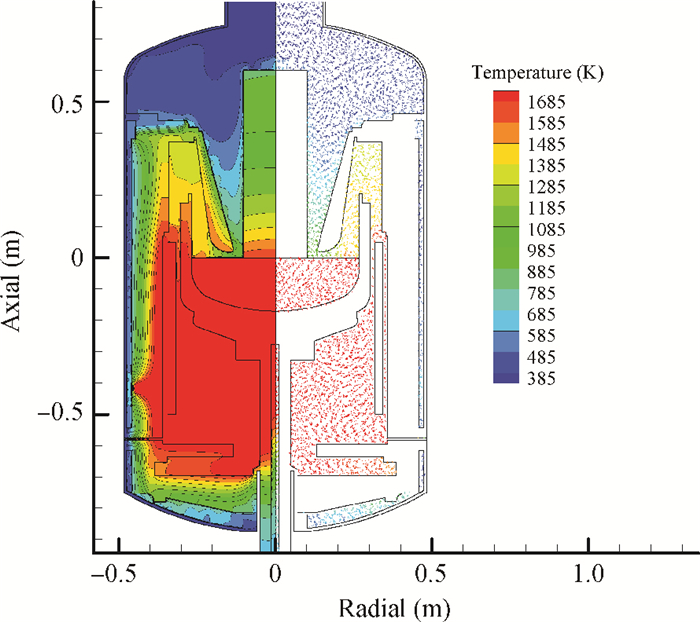
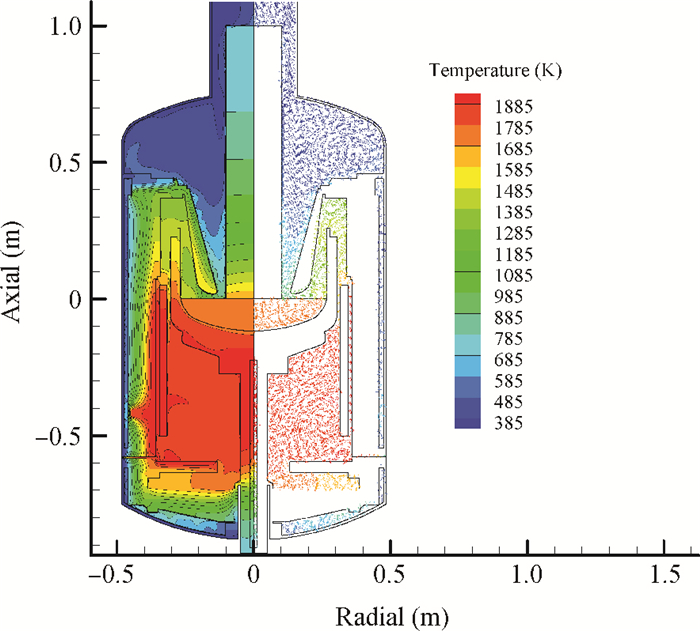
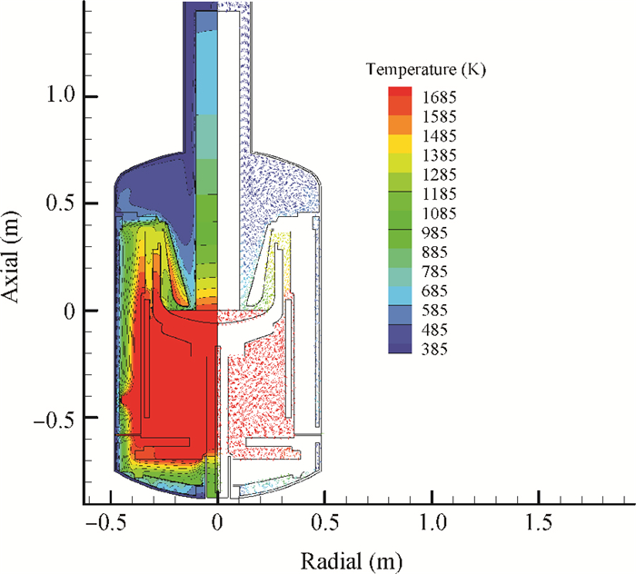
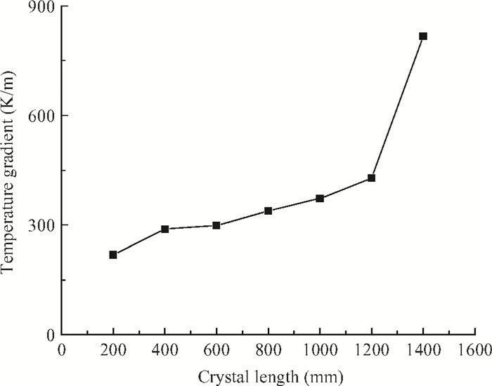
A global analysis of heat transfer and fluid flow in a real Czochralski single silicon crystal furnace is developed using the FLUENT package. Good agreement was obtained for comparisons of the power and crystal growth speed between the simulation and experimental data, and the effect of the length of the crystal on heat transfer and fluid flow was analyzed. The results showed that Tmax increases and its location moves downward as the crystal length increases. The flow pattern in the melt does not change until the crystal grows to 900 mm. As the crystal length increases, the flow pattern in the first gas area only changes when the crystal length is less than 700 mm, but the flow pattern in the second area changes throughout the growth process.


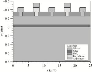
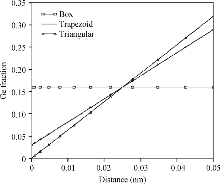
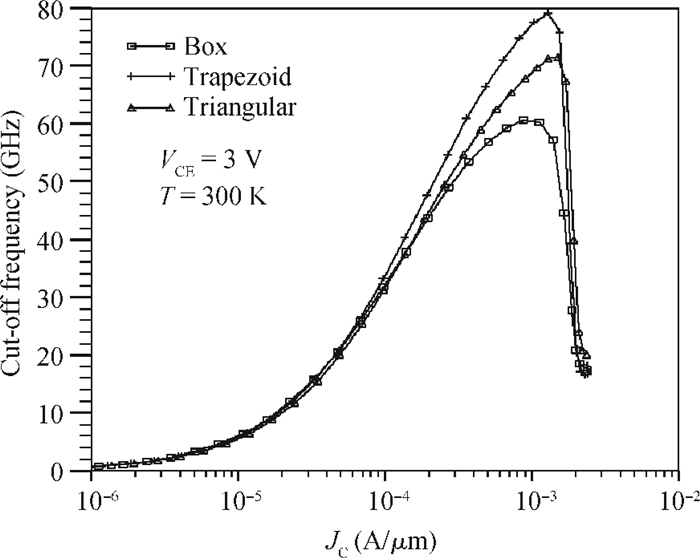
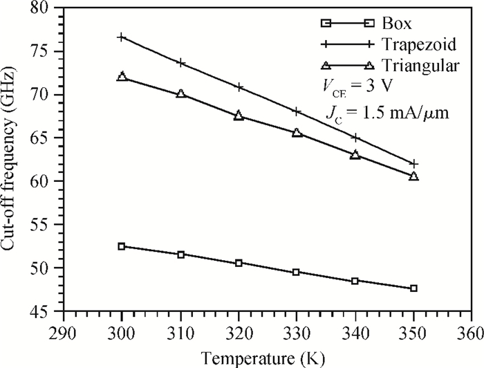
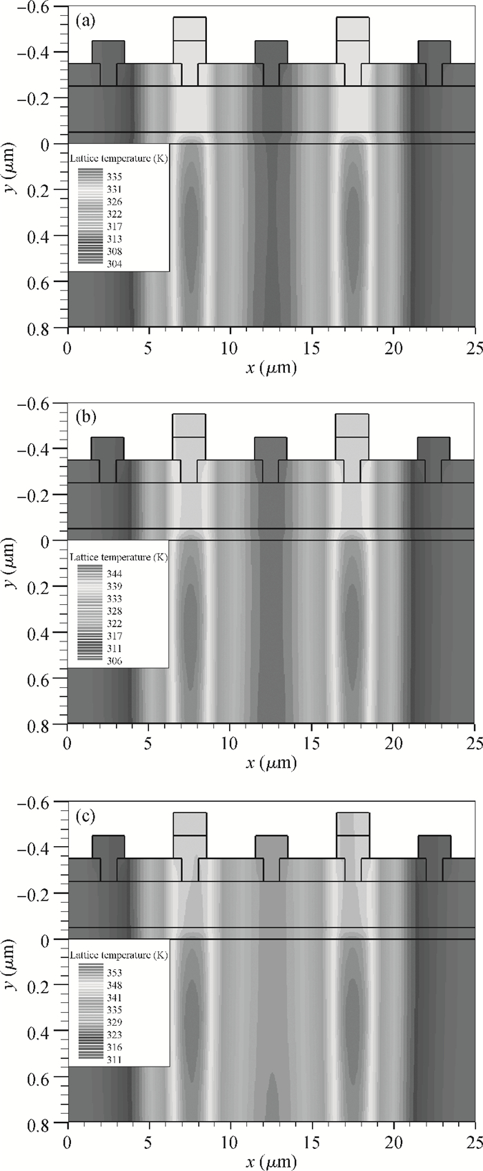
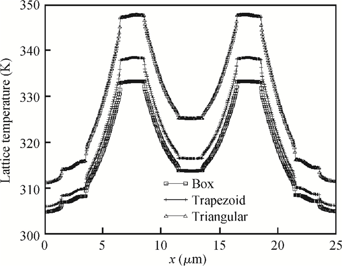
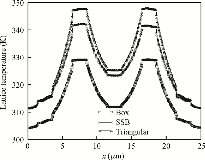
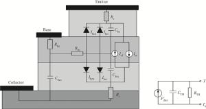
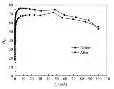
The impact of the three state-of-the-art germanium (Ge) profiles (box, trapezoid and triangular) across the base of SiGe heterojunction bipolar transistors (HBTs) under the condition of the same total amount of Ge on the temperature dependence of current gain β and cut-off frequency fT, as well as the temperature profile, are investigated. It can be found that although the β of HBT with a box Ge profile is larger than that of the others, it decreases the fastest as the temperature increases, while the β of HBT with a triangular Ge profile is smaller than that of the others, but decreases the slowest as the temperature increases. On the other hand, the fT of HBT with a trapezoid Ge profile is larger than that of the others, but decreases the fastest as the temperature increases, and the fT of HBT with a box Ge profile is smaller than that of the others, but decreases the slowest as temperature increases. Furthermore, the peak and surface temperature difference between the emitter fingers of the HBT with a triangular Ge profile is higher than that of the others. Based on these results, a novel segmented step box Ge profile is proposed, which has modest β and fT, and trades off the temperature sensitivity of current gain and cut-off frequency, and the temperature profile of the device.


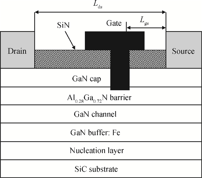
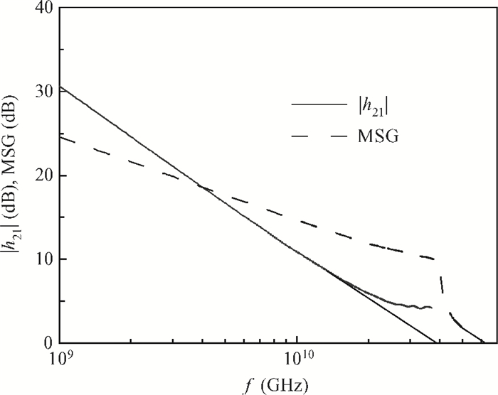
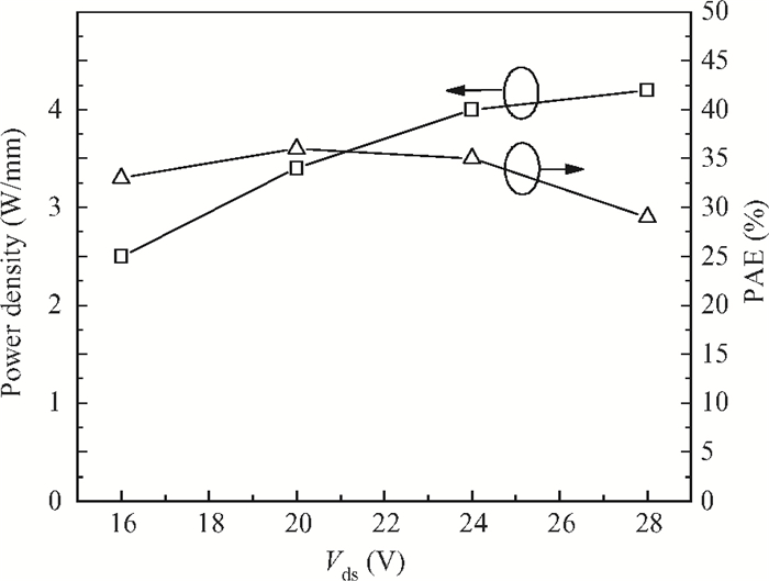
SiN dielectrically-defined 0.15 μm field plated GaN HEMTs for millimeter-wave application have been presented. The AlGaN/GaN hetero-structure epitaxial material for HEMTs fabrication was grown on a 3-inch SiC substrate with an Fe doped GaN buffer layer by metal-organic chemical deposition. Electron beam lithography was used to define both the gate footprint and the cap of the gate with an integrated field plate. Gate recessing was performed to control the threshold voltage of the devices. The fabricated GaN HEMTs exhibited a unit current gain cut-off frequency of 39 GHz and a maximum frequency of oscillation of 63 GHz. Load-pull measurements carried out at 35 GHz showed a power density of 4 W/mm with associated power gain and power added efficiency of 5.3 dB and 35%, respectively, for a 0.15 mm gate width device operated at a 24 V drain bias. The developed 0.15 μm gate length GaN HEMT technology is suitable for Ka band applications and is ready for millimeter-wave power MMICs development.


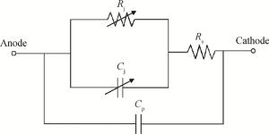
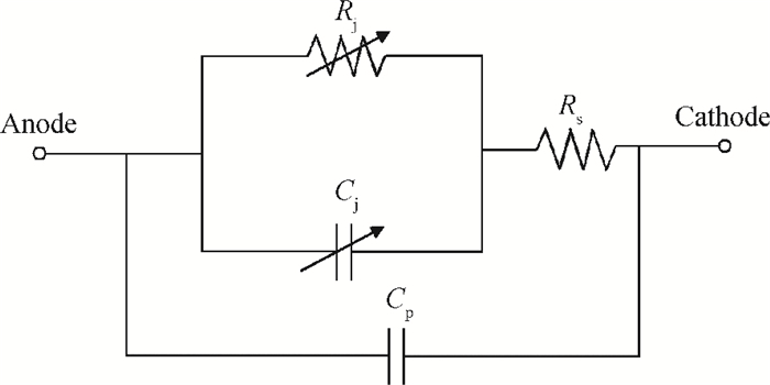
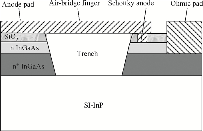
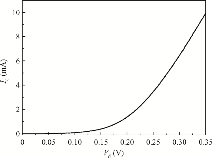
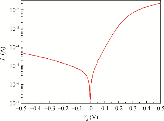
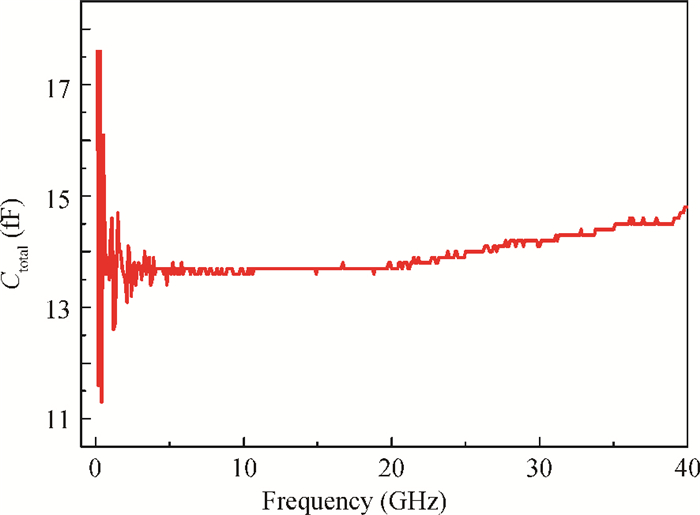
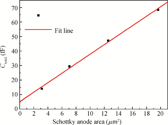
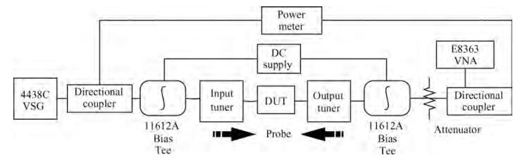
Based on characteristics such as low barrier and high electron mobility of lattice matched In0.53Ga0.47 As layer, InP-based Schottky barrier diodes (SBDs) exhibit the superiorities in achieving a lower turn-on voltage and series resistance in comparison with GaAs ones. Planar InP-based SBDs have been developed in this paper. Measurements show that a low forward turn-on voltage of less than 0.2 V and a cutoff frequency of up to 3.4 THz have been achieved. The key factors of the diode such as series resistance and the zero-biased junction capacitance are measured to be 3.32 Ω and 9.1 fF, respectively. They are highly consistent with the calculated values. The performances of the InP-based SBDs in this work, such as low noise and low loss, are promising for applications in the terahertz mixer, multiplier and detector circuits.

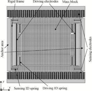
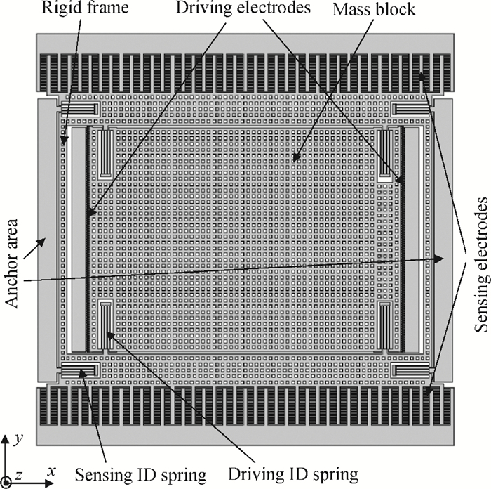
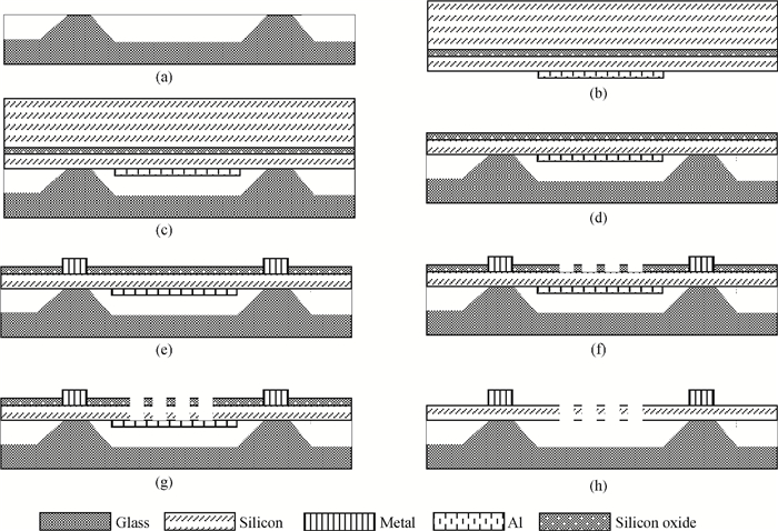
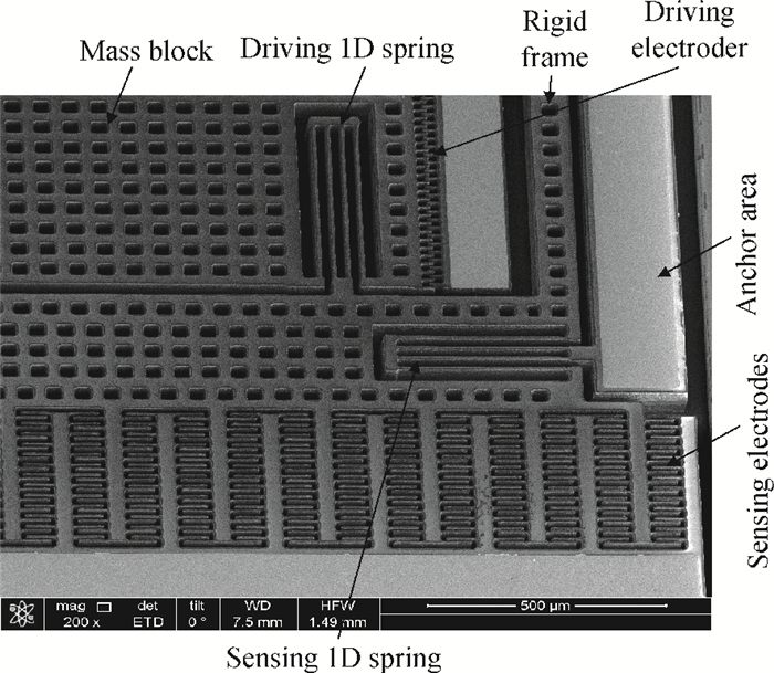
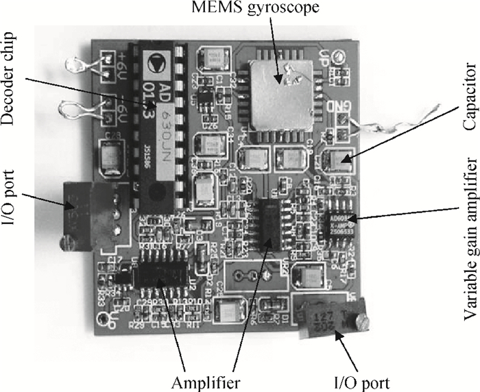
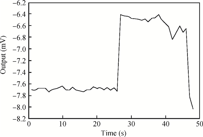
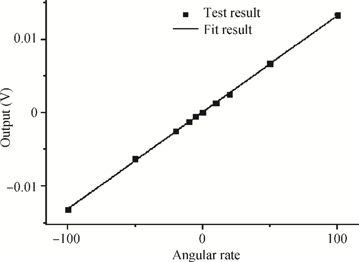
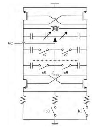
This paper presents an SOI (silicon on insulator) MEMS (micro-electro-mechanical systems) vibratory gyroscope that was fabricated using bulk micromachining processes. In the gyroscope architecture, a frame structure that nests the proof mass is used to decouple the drive motion and sense motion. This approach ensures that the drive motion is well aligned with the designed drive axis, and minimizes the actual drive motion component along the sense detection axis. The thickness of the structural layer of the device is 100 μm, which induces a high elastic stiffness in the thickness direction, so it can suppress the high-order out-of-plane resonant modes to reduce deviation. In addition, the dynamics of the gyroscope indicate that higher driving mass brings about higher sensing displacements. The thick structural layer can improve the output of the device by offering a sufficient mass weight and large sensing capacitance. The preliminary test results of the vacuum packaged device under atmospheric pressure will be provided. The scale factor is 1.316×10⁻⁴ V/(deg/s), the scale factor nonlinearity and asymmetry are 1.87% and 0.36%, the zero-rate offset is 7.74×10⁻⁴ V, and the zero-rate stability is 404 deg/h, respectively.
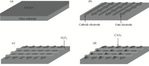
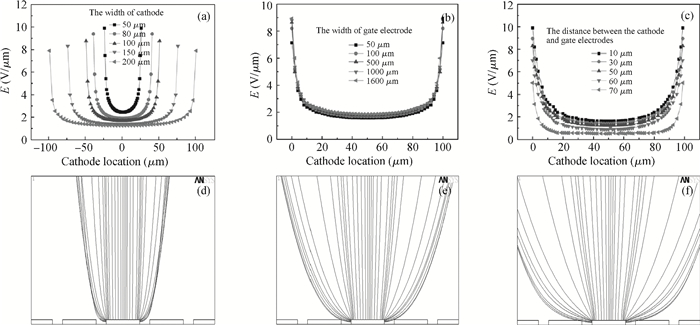
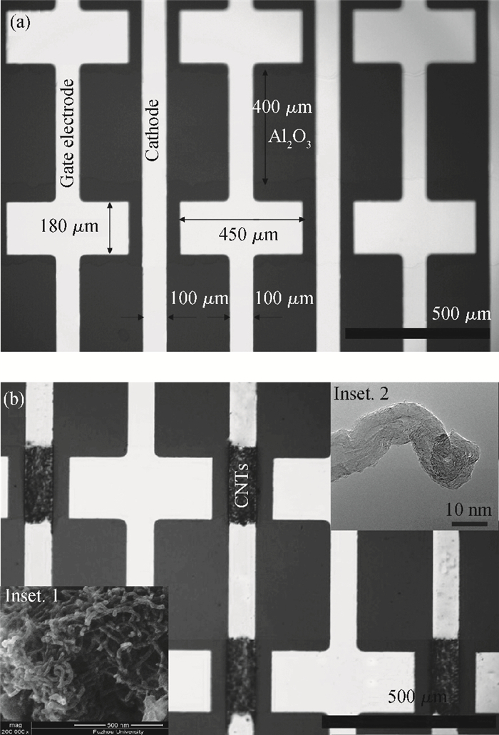
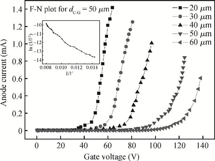
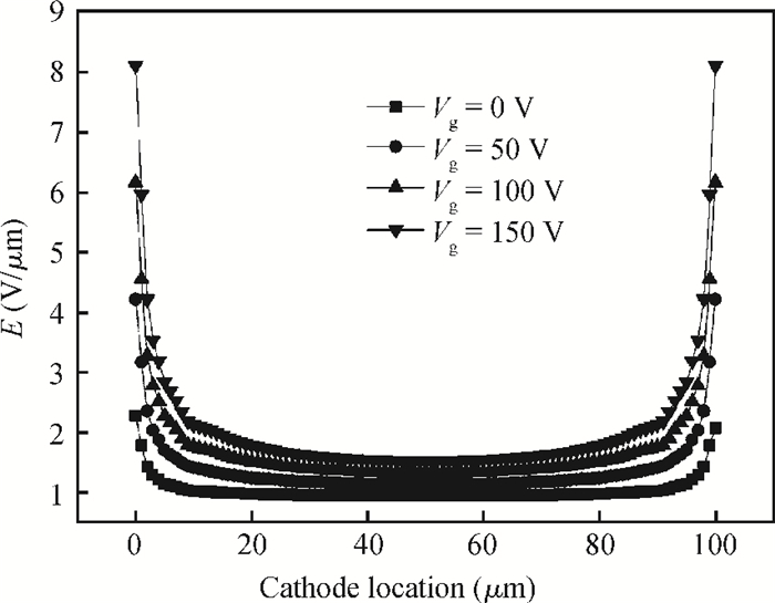
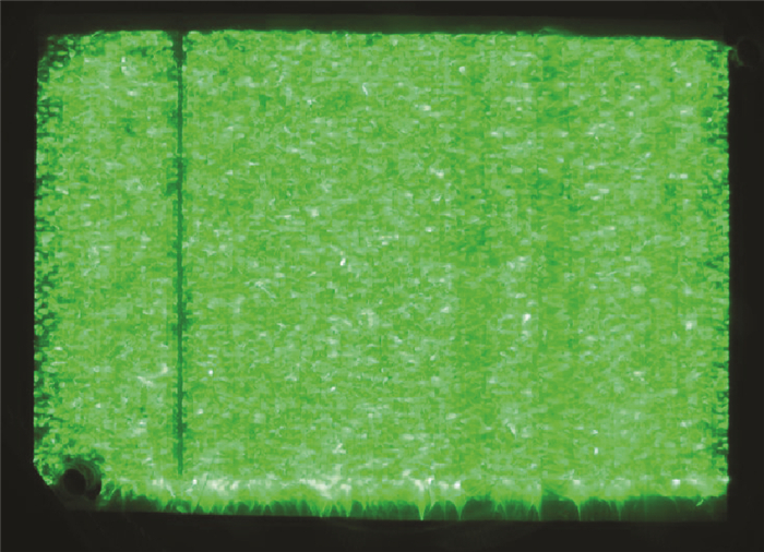
This paper describes the fabrication of backlight units (BLUs) for a liquid crystal display (LCD) based on a novel planar-gate electron source with patterned carbon nanotubes (CNTs) formed by electrophoretic deposition. The electric field distributions and electron trajectories of this triode structure are simulated according to Ansys software. The device structure is optimized by supporting numerical simulation. The field emission results show that the emission current depends strongly on the cathode-gate gap and the gate voltage. Direct observation of the luminous images on a phosphor screen reveals that the electron beams undergo a noticeable expansion along the lateral direction with increasing gate voltage, which is in good agreement with the simulation results. The luminous efficiency and luminance of the fabricated device reaches 49.1 lm/W and 5500 cd/m2, respectively. All results indicate that the novel planar-gate electron source with patterned CNTs may lead to practical applications for an electron source based on a flat lamp for BLUs in LCD.


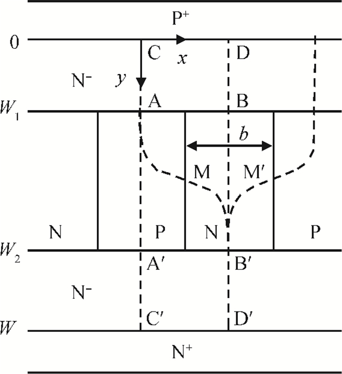
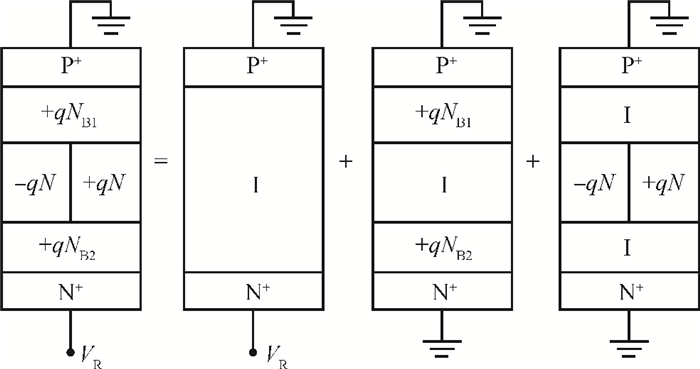
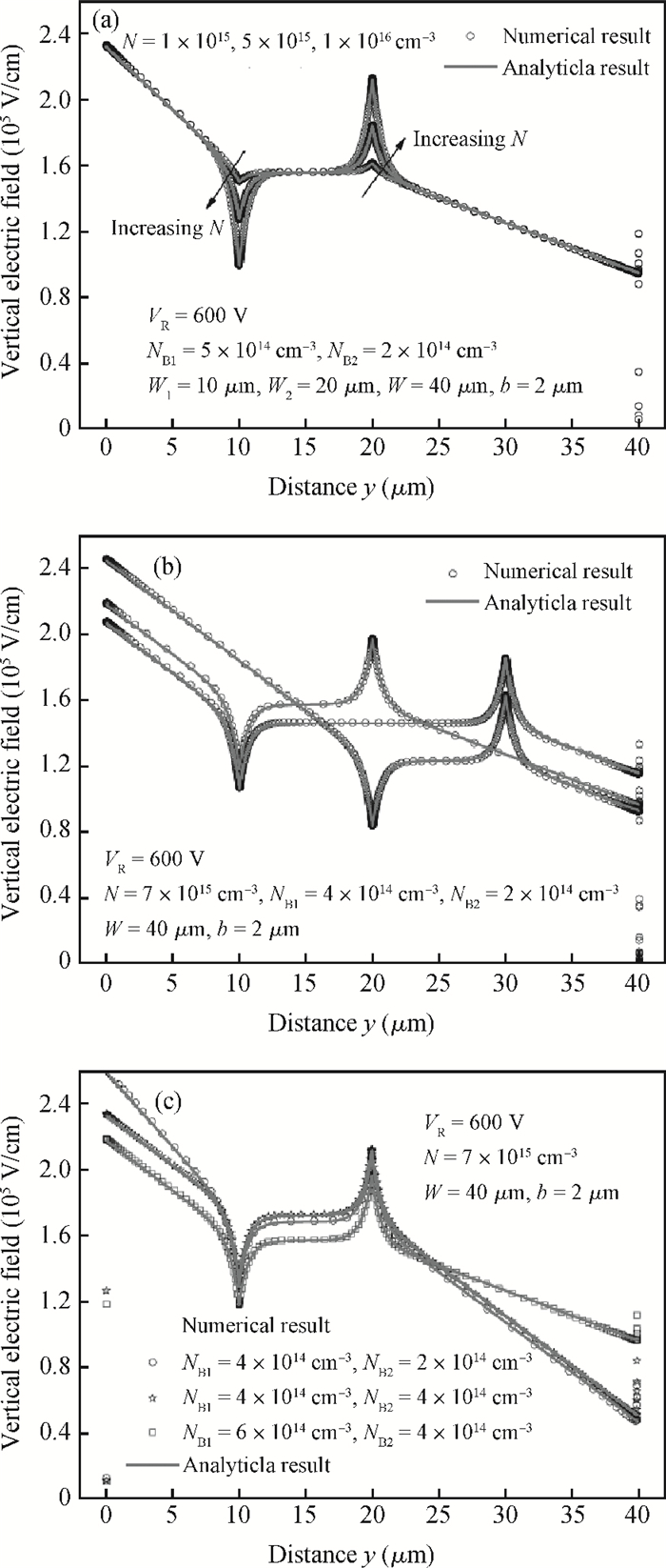
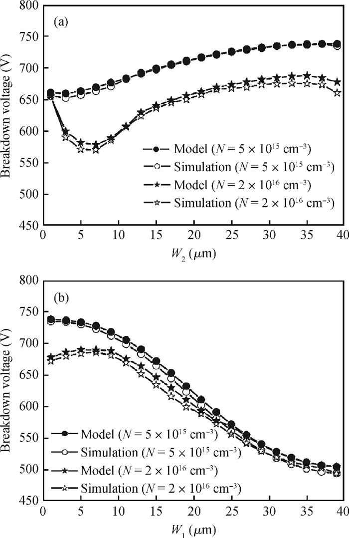
An analytical model of the electric field distributions of buried superjunction structures, based on the charge superposition method and Green's function approach, is derived. An accurate approximation of the exact analytical model of the vertical electric field is also proposed and demonstrated by numerical simulation. The influence of the dimension and doping concentration of each layer on the electric field is discussed in detail, and the breakdown voltage is demonstrated by simulations.

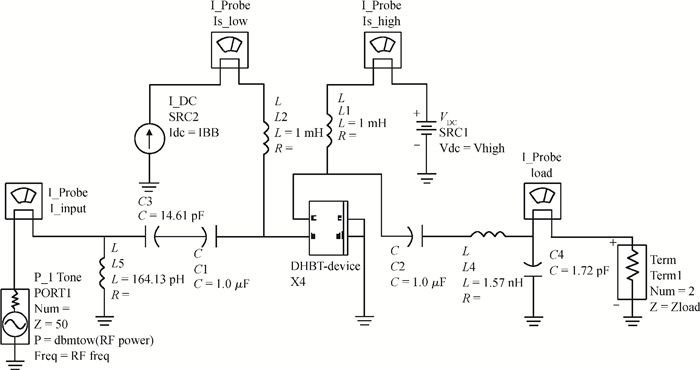
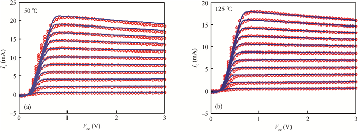
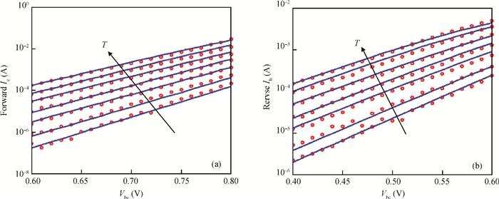
A large signal model for InP/InGaAs double heterojunction bipolar transistors including thermal effects has been reported, which demonstrated good agreements of simulations with measurements. On the basis of the previous model in which the double heterojunction effect, current blocking effect and high current effect in current expression are considered, the effect of bandgap narrowing with temperature has been considered in transport current while a formula for model parameters as a function of temperature has been developed. This model is implemented by Verilog-A and embedded in ADS. The proposed model is verified with DC and large signal measurements.


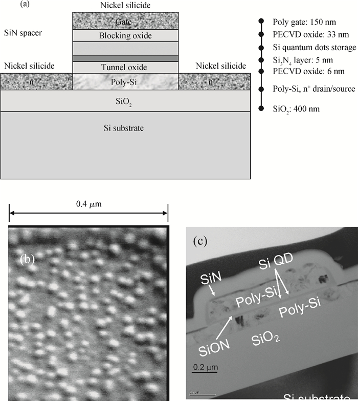
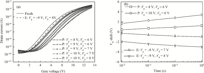
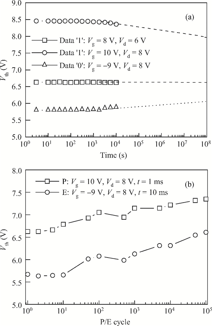
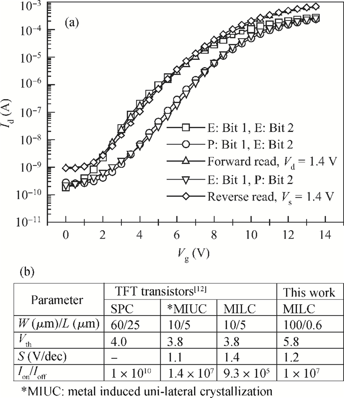
This paper reports on a successful demonstration of poly-Si TFT nonvolatile memory with a much reduced thermal-budget. The TFT uses uniform Si quantum-dots (size 10 nm and density 1011 cm-2) as storage media, obtained via LPCVD by flashing SiH4/H2 at 580℃ for 15 s on a Si3N4 surface. The poly-Si grain-enlargement step was shifted after source/drain formation. The NiSix-silicided source/drain enables a fast lateral-recrystallization, and thus grain-enlargement can be accomplished by a much reduced thermal-cycle (i.e., 550℃/4 h). The excellent memory characteristics suggest that the proposed poly-Si TFT Si quantum-dot memory and associated processes are promising for use in wider TFT applications, such as system-on-glass.
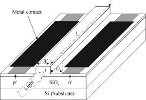
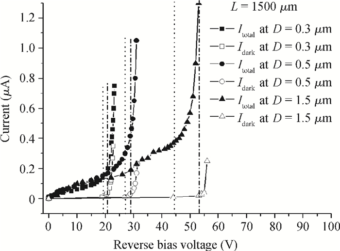
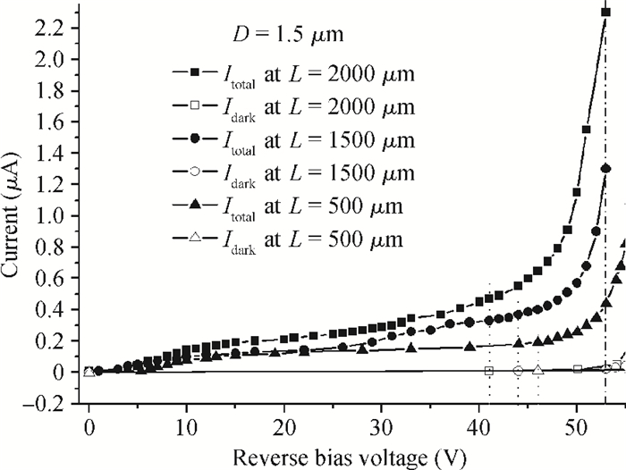
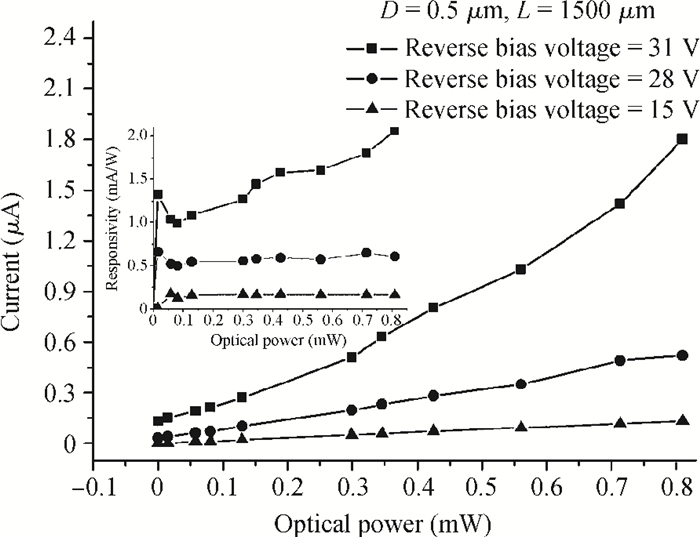
The photocurrent effect in pin silicon waveguides at 1550 nm wavelength is experimentally investigated. The photocurrent is mainly attributed to surface-state absorption, defect-state absorption and/or two-photon absorption. Experimental results show that the photocurrent is enhanced by the avalanche effect. A pin silicon waveguide with an intrinsic region width of 3.4 μm and a length of 2000 μm achieves a responsivity of 4.6 mA/W and an avalanche multiplication factor of about five.
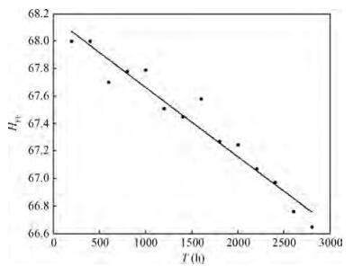
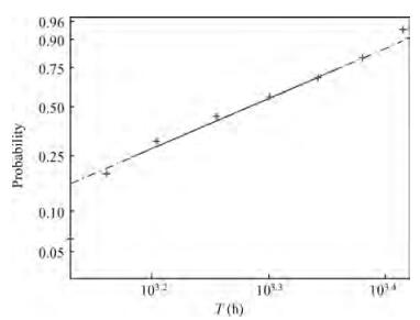
Choosing small and medium power switching transistors of the NPN type in a 3DK set as the study object, the test of accelerating life is conducted in constant temperature and humidity, and then the data are statistically analyzed with software developed by ourselves. According to degradations of such sensitive parameters as the reverse leakage current of transistors, the lifetime order of transistors is about more than 104 at 100℃ and 100% relative humidity (RH) conditions. By corrosion fracture of transistor outer leads and other failure modes, with the failure truncated testing, the average lifetime rank of transistors in different distributions is extrapolated about 103. Failure mechanism analyses of degradation of electrical parameters, outer lead fracture and other reasons that affect transistor lifetime are conducted. The findings show that the impact of external stress of outer leads on transistor reliability is more serious than that of parameter degradation.


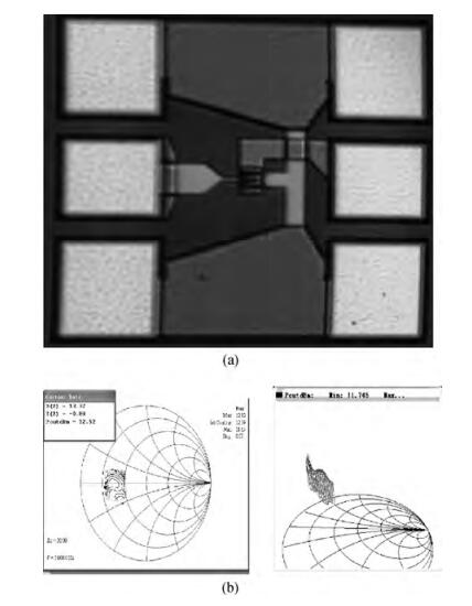
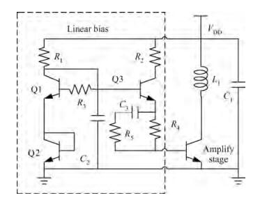
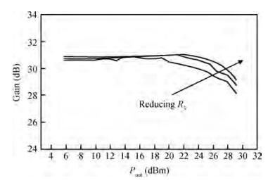
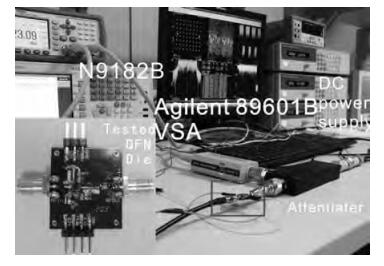
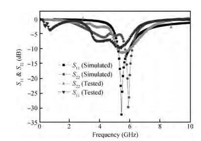
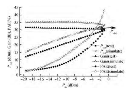
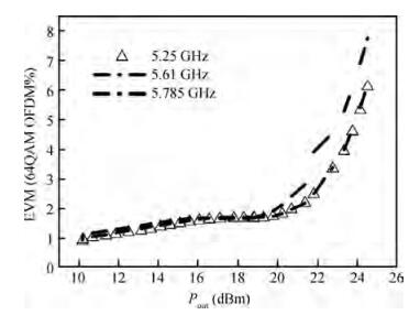
A three-stage 4.8-6 GHz monolithic power amplifier (PA) compatible with IEEE 802.11a/n designed based on an advanced 2 μm InGaP/GaAs hetero-junction bipolar transistor (HBT) process is presented. The PA integrates input matching and closed-loop power control circuits on chip. Under 3.3 V DC bias, the amplifier achieves a 31 dB small signal gain, excellent wide band input and output matching among overall 1.2 GHz bandwidth, and up to 24.5 dBm linear output power below EVM 3% with IEEE 802.11a 64QAM OFDM input signal.


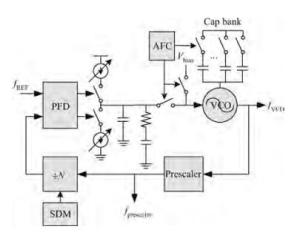
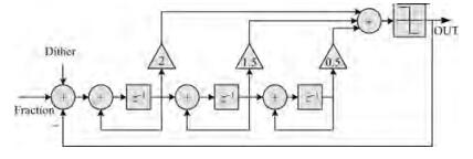
A wide range fractional-N frequency synthesizer in 0.18 μm RF CMOS technology is implemented. A switched-capacitors bank LC-tank VCO and an adaptive frequency calibration technique are used to expand the frequency range. A 16-bit third-order sigma-delta modulator with dither is used to randomize the fractional spur. The active area is 0.6 mm2. The experimental results show the proposed frequency synthesizer consumes 4.3 mA from a single 1.8 V supply voltage except for buffers. The frequency range is 1.44-2.11 GHz and the frequency resolution is less than 0.4 kHz. The phase noise is-94 dBc/Hz@100 kHz and-121 dBc/Hz@1 MHz at the output of the prescaler with a loop bandwidth of approximately 120 kHz. The performance meets the requirements for the multi-band and multi-mode transceiver applications.


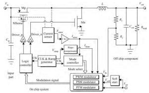
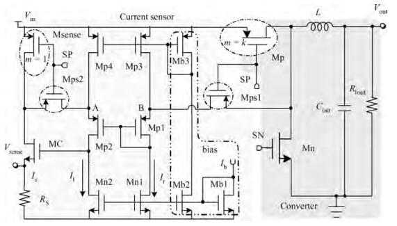
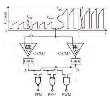
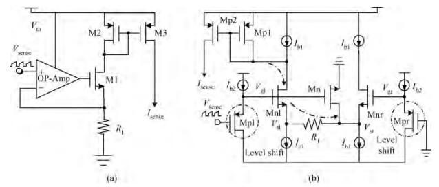
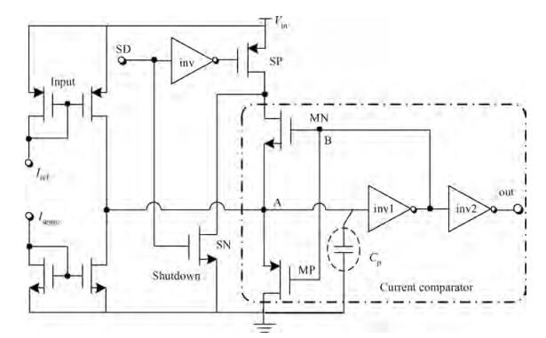
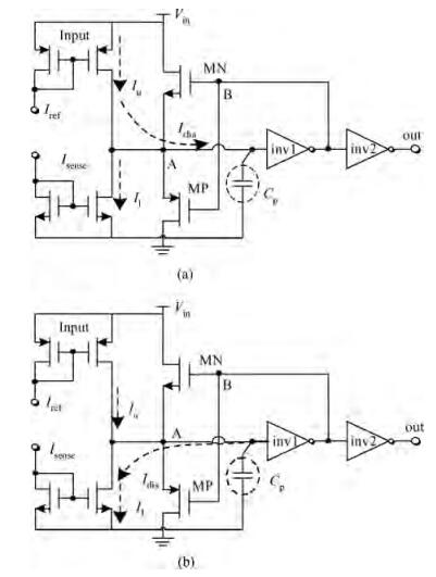
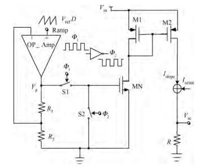
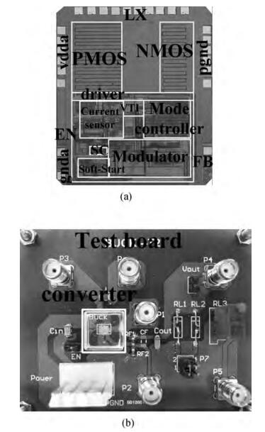
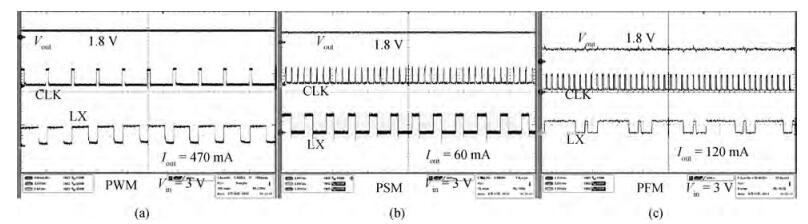
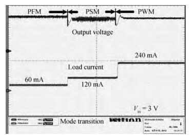
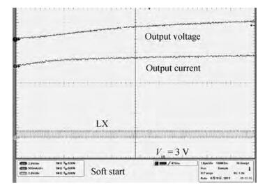
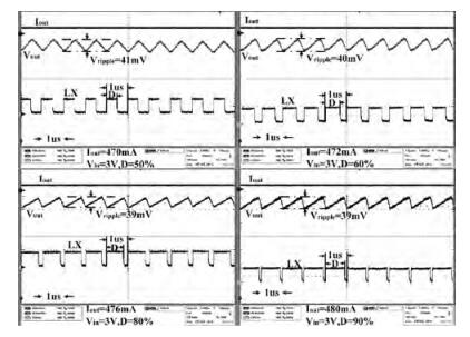
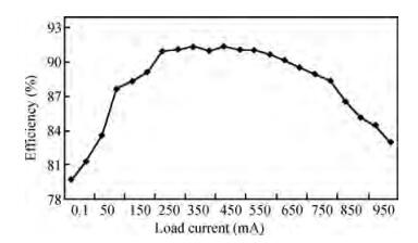
A synchronous buck DC-DC converter with an adaptive multi-mode controller is proposed. In order to achieve high efficiency over its entire load range, pulse-width modulation (PWM), pulse-skip modulation (PSM) and pulse-frequency modulation (PFM) modes were integrated in the proposed DC-DC converter. With a highly accurate current sensor and a dynamic mode controller on chip, the converter can dynamically change among PWM, PSM and PFM control according to the load requirements. In addition, to avoid power device damage caused by inrush current at the start up state, a soft-start circuit is presented to suppress the inrush current. Furthermore, an adaptive slope compensation (SC) technique is proposed to stabilize the current programmed PWM controller for duty cycle passes over 50%, and improve the degraded load capability due to traditional slope compensation. The buck converter chip was simulated and manufactured under a 0.35 μm standard CMOS process. Experimental results show that the chip can achieve 79% to 91% efficiency over the load range of 0.1 to 1000 mA.


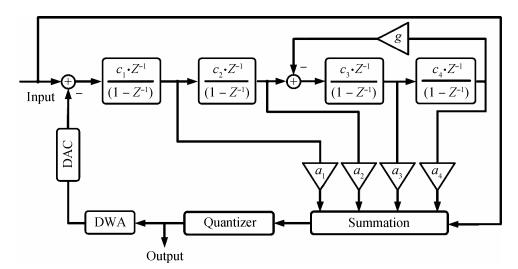
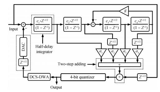
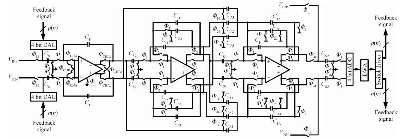
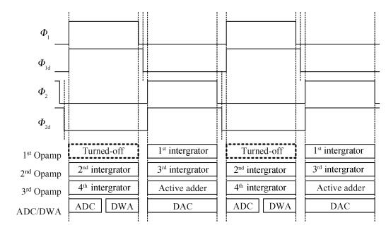
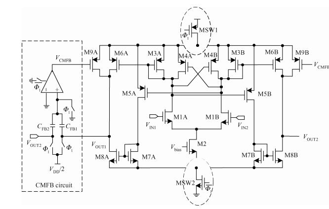
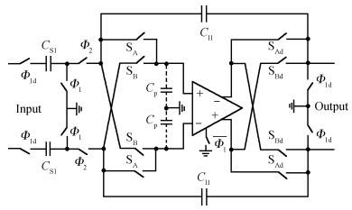
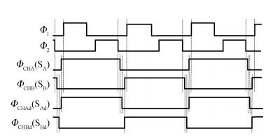
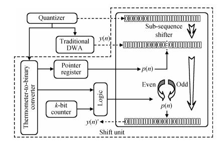
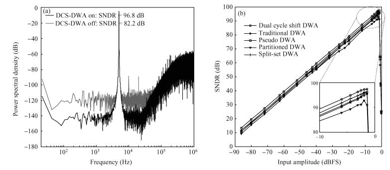
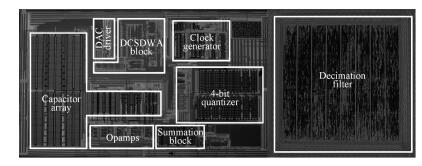
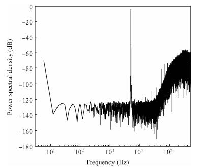
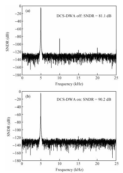
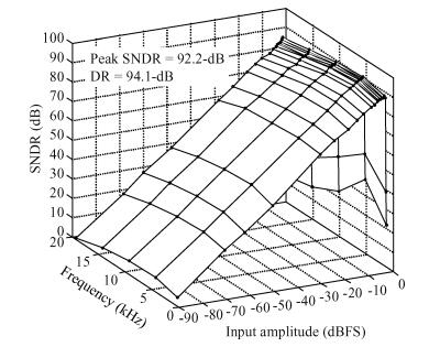
This paper presents a low-power high-precision switched-opamp (SO)-based delta-sigma (Δ Σ) analog-to-digital converter (ADC). The proposed SO design allows circuit operation at sub-1 V supply voltage, only needs to work in half of a clock cycle, and thus is suitable for low power applications. In addition, an opamp-sharing technique is applied to save on hardware overheads. Due to the use of a dual cycle shift data weighted averaging (DCS-DWA) technique, mismatch errors caused in the feedback DAC have been eliminated without introducing signal-dependent tones. The proposed ADC has been implemented in a standard 0.18 μm process and measured to have a 92.2 dB peak SNDR and 94.1 dB dynamic range with 25 kHz signal bandwidth. The power consumption is 58 μ W for the modulator at 0.9 V supply voltage and 96 μ W for the decimation filter, which translate to the figure-of-merit (FOM) of 35.4 fJ/step for the solo modulator, and 94 fJ/step for the whole system.


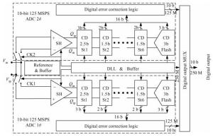
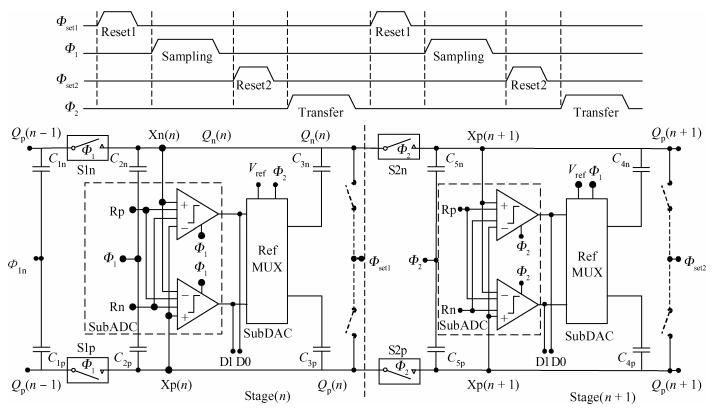
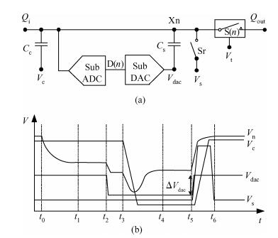
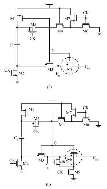
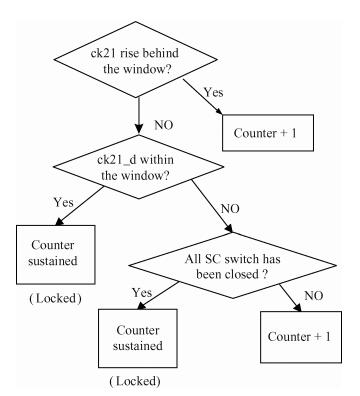
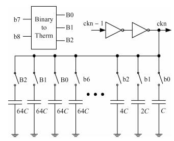
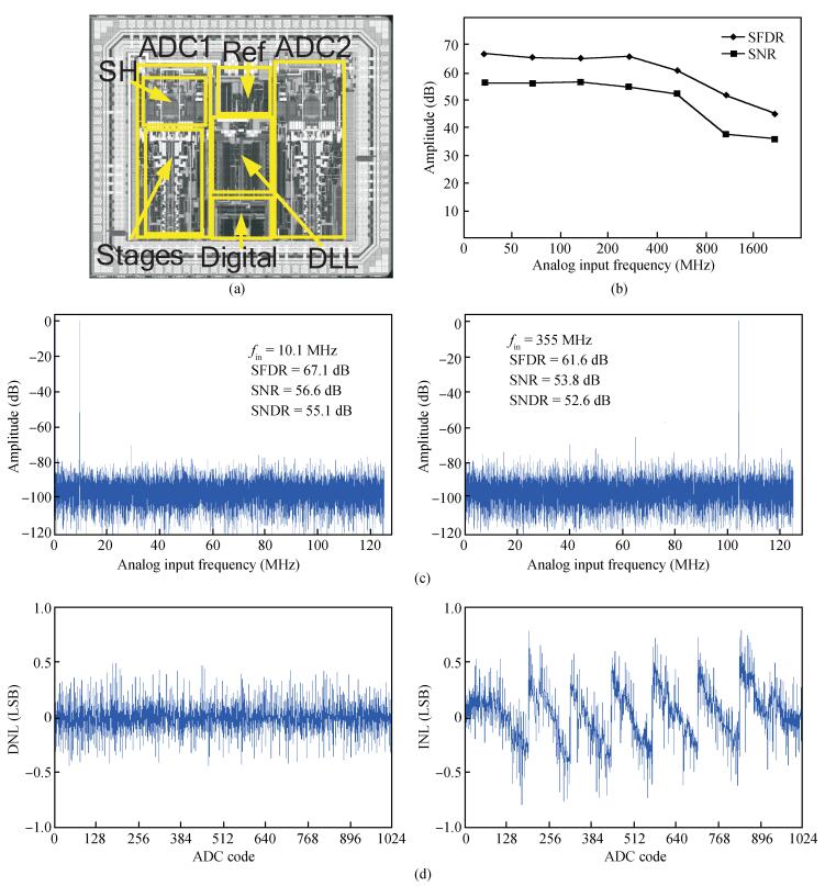
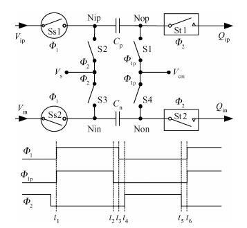
A 10-bit 250-MSPS two-channel time-interleaved charge-domain (CD) pipelined analog-to-digital converter (ADC) is presented. MOS bucket-brigade device (BBD) based CD pipelined architecture is used to achieve low power consumption. An all digital low power DLL is used to alleviate the timing mismatches and to reduce the aperture jitter. A new bootstrapped MOS switch is designed in the sample and hold circuit to enhance the IF sampling capability. The ADC achieves a spurious free dynamic range (SFDR) of 67.1 dB, signal-to-noise ratio (SNDR) of 55.1 dB for a 10.1 MHz input, and SFDR of 61.6 dB, SNDR of 52.6 dB for a 355 MHz input at full sampling rate. Differential nonlinearity (DNL) is +0.5/-0.4 LSB and integral nonlinearity (INL) is +0.8/-0.75 LSB. Fabricated in a 0.18-μm 1P6M CMOS process, the prototype 10-bit pipelined ADC occupies 1.8×1.3 mm2 of active die area, and consumes only 68 mW at 1.8 V supply.


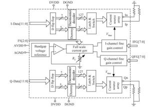
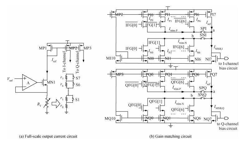
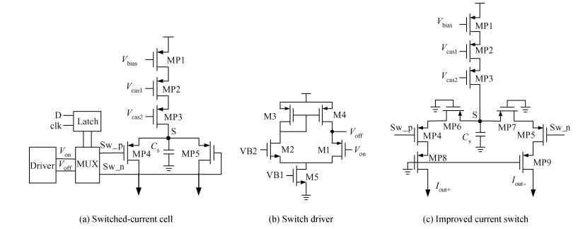
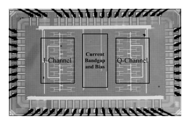
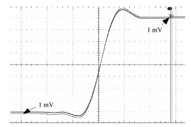
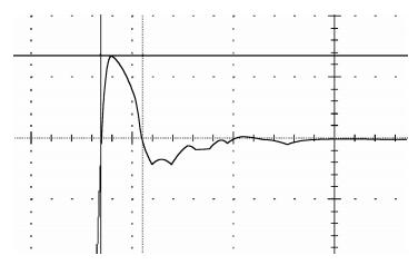
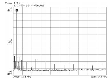
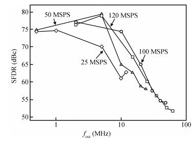
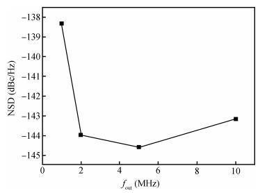
This paper presents a two-channel 12-bit current-steering digital-to-analog converter (DAC) for I and Q signal paths in a wireless transmitter. The proposed DAC has a full-scale output current with an adjusting range of 2 to 10 mA. A gain matching circuit is proposed to reduce gain mismatch between the I and Q channels. The tuning range is ±24% of full scale and the minimum resolution is 1/16 LSB. To further improve its dynamic performance, the switch driver and current cell are optimized to minimize glitch energy. The chip has been processed in a standard 0.13 μm CMOS technology. Gain mismatch between a I-channel DAC and a Q-channel DAC is measured to be approximately 0.13%. At 120-MSPS sample rate for 1 MHz sinusoidal signal, the spurious free dynamic range (SFDR) is 75 dB. The total power dissipation is 62 mW and has an active area of 1.08 mm2.

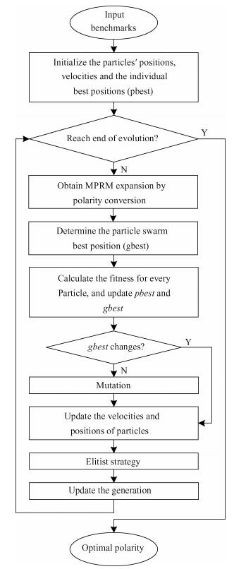
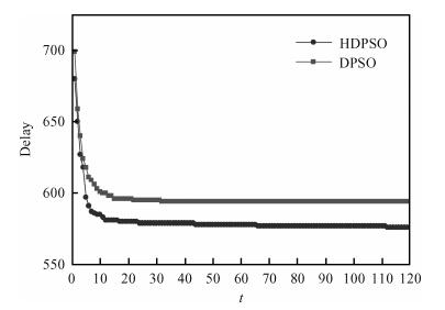
Polarity optimization for mixed polarity Reed-Muller (MPRM) circuits is a combinatorial issue. Based on the study on discrete particle swarm optimization (DPSO) and mixed polarity, the corresponding relation between particle and mixed polarity is established, and the delay-area trade-off of large-scale MPRM circuits is proposed. Firstly, mutation operation and elitist strategy in genetic algorithm are incorporated into DPSO to further develop a hybrid DPSO (HDPSO). Then the best polarity for delay and area trade-off is searched for large-scale MPRM circuits by combining the HDPSO and a delay estimation model. Finally, the proposed algorithm is testified by MCNC Benchmarks. Experimental results show that HDPSO achieves a better convergence than DPSO in terms of search capability for large-scale MPRM circuits.

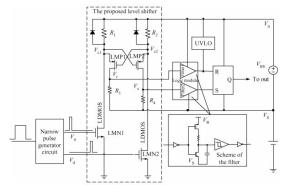
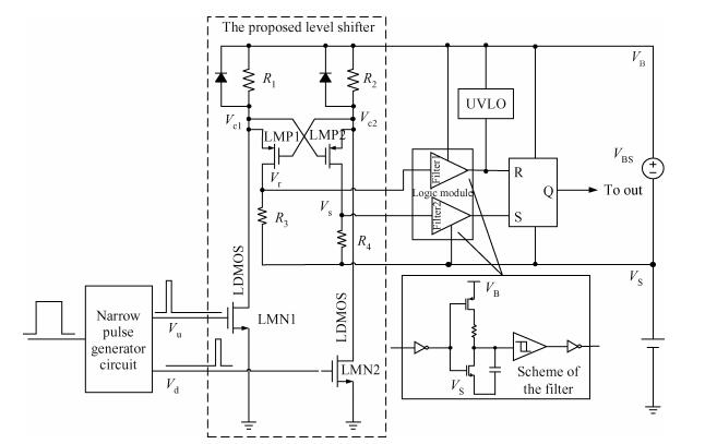
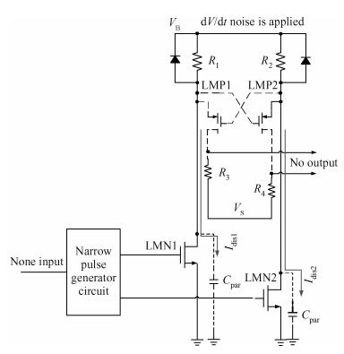
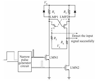
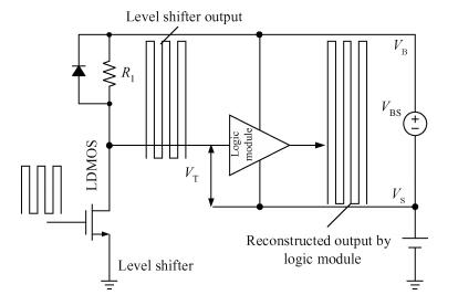
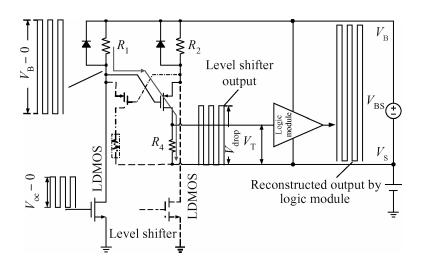
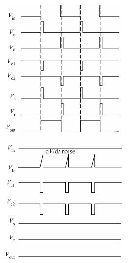
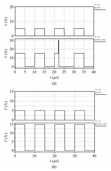
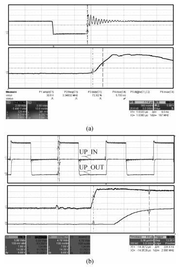
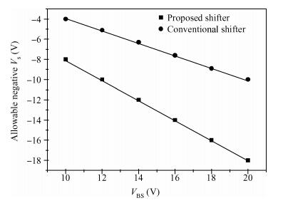
A novel level shift circuit featuring with high dV/dt noise immunity and improved negative VS capacity is proposed in this paper. Compared with the conventional structure, the proposed circuit adopting two cross-coupled PMOS transistors realizes the selective filtering ability by exploiting the path which filters out the noise introduced by the dV/dt. In addition, a differential noise cancellation circuit is proposed to enhance the noise immunity further. Meanwhile, the negative VS capacity is improved by unifying the detected reference voltage and the logic block's threshold voltage. A high voltage half bridge gate drive IC adopting the presented structure is experimentally realized by using a usual 600 V BCD process and achieves the stable operation up to 65 V/ns of the dV/dt characteristics.

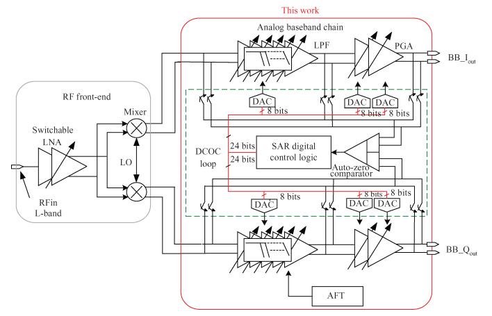
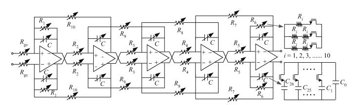
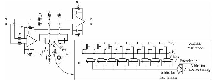
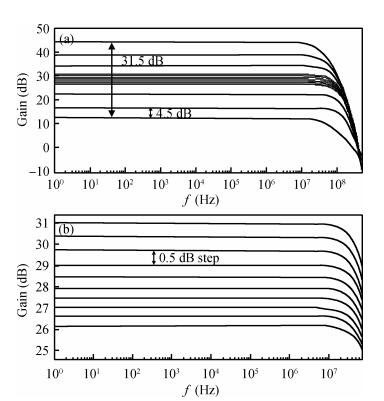
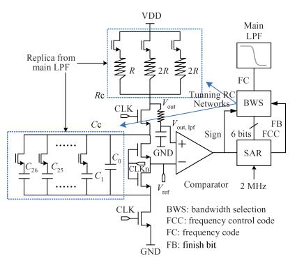
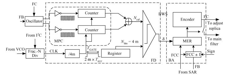
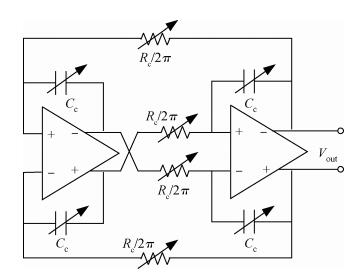
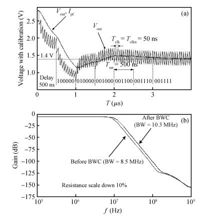
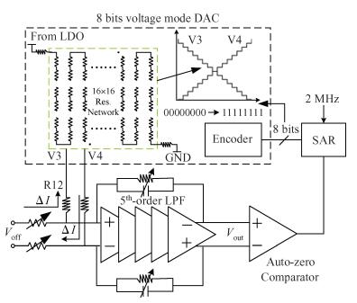
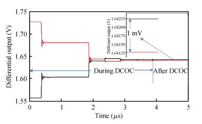
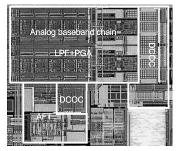
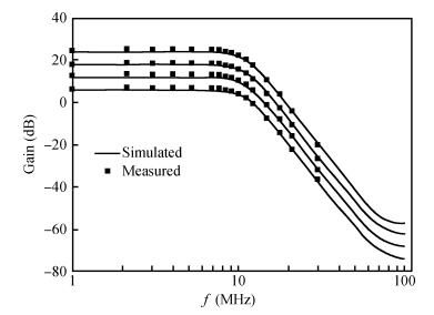
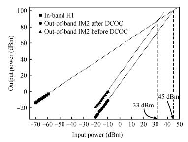
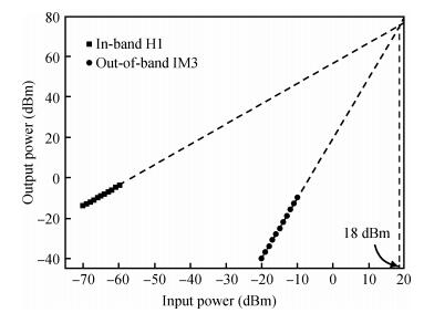
This paper presents a continuously and widely tunable analog baseband chain with a digital-assisted calibration scheme implemented on a 0.13 μm CMOS technology. The analog baseband is compliant with several digital broadcasting system (DBS) standards, including DVB-S, DVB-S2, and ABS-S. The cut-off frequency of the baseband circuit can be changed continuously from 4.5 to 32 MHz. The gain adjustment range is from 6 to 55.5 dB with 0.5 dB step. The calibration includes automatic frequency tuning (AFT) and automatic DC offset calibration (DCOC) to achieve less than 6% cut-off frequency deviation and 3 mV residual output offset. The out-of-band ⅡP2 and ⅡP3 of the overall chain are 45 dBm and 18 dBm respectively, while the input referred noise (IRN) is 17.4 nV/$\sqrt{\rm Hz}$ All circuit blocks are operated at 2.8 V from LDO and consume current of 20.4 mA in the receiving mode.


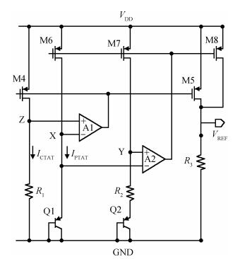
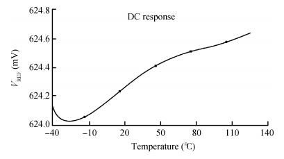
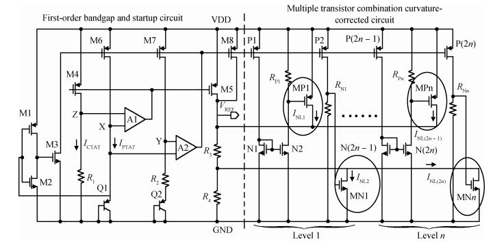
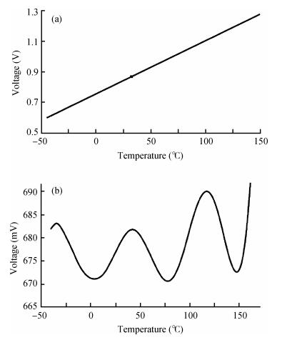
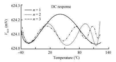
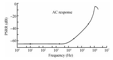
A new bandgap reference (BGR) curvature compensation technology is proposed, which is a kind of multiple transistor combination. On the basis of the existing first-order bandgap reference technology, a compensation current circuit consisting of a sink current branch and a source current branch is added. The BGR was designed and simulated by using Semiconductor Manufacturing International Corporation (SMIC) 0.18 μm CMOS process. The simulation results showed that when the power supply voltage was 1 V, the temperature coefficient of the BGR was 2.08 ppm/℃ with the temperature range from-40 to 125℃, the power supply rejection ratio (PSRR) was-64.77 dB and the linear regulation was 0.44 mV/V with the supply power changing from 0.85 to 1.8 V.


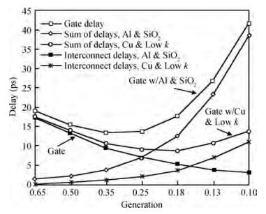
In this paper, a review of Cu/low-k, carbon nanotube (CNT), graphene nanoribbon (GNR) and optical based interconnect technologies has been done. Interconnect models, challenges and solutions have also been discussed. Of all the four technologies, CNT interconnects satisfy most of the challenges and they are most suited for nanometer scale technologies, despite some minor drawbacks. It is concluded that beyond 32 nm technology, a paradigm shift in the interconnect material is required as Cu/low-k interconnects are approaching fundamental limits.


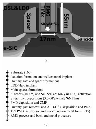
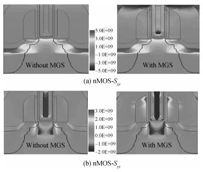
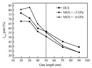
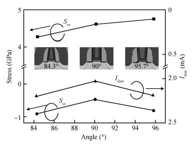
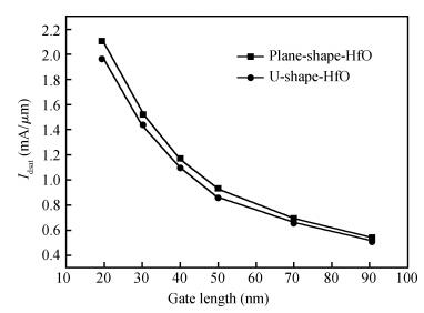
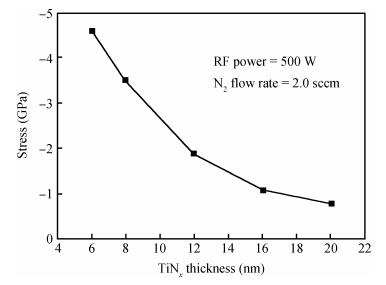
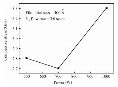
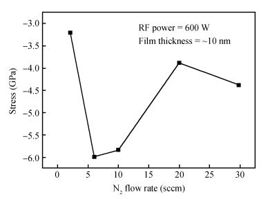
The optimizations to metal gate structure and film process were extensively investigated for great metal-gate stress (MGS) in 20 nm high-k/metal-gate-last (HK/MG-last) nMOS devices. The characteristics of advanced MGS technologies on device performances were studied through a process and device simulation by TCAD tools. The metal gate electrode with different stress values (0 to-6 GPa) was implemented in the device simulation along with other traditional process-induced-strain (PIS) technologies like e-SiC and nitride capping layer. The MGS demonstrated a great enhancing effect on channel carriers transporting in the device as device pitch scaling down. In addition, the novel structure for a tilted gate electrode was proposed and relationships between the tilt angle and channel stress were investigated. Also with a new method of fully stressed replacement metal gate (FSRMG) and using plane-shape-HfO to substitute U-shape-HfO, the effect of MGS was improved. For greater film stress in the metal gate, the process conditions for physical vapor deposition (PVD) TiNx were optimized. The maximum compressive stress of-6.5 GPa TiNx was achieved with thinner film and greater RF power as well as about 6 sccm N ratio.


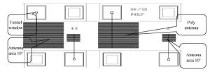
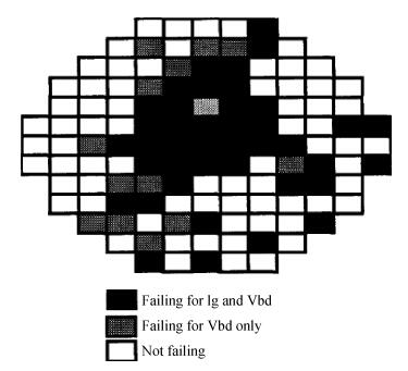
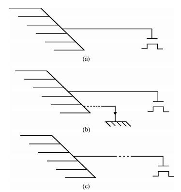
A comparison is made of several plasma-induced damage (PID) measurement techniques. A novel PID mechanism using high-density plasma (HDP) inter-metal dielectric (IMD) deposition is proposed. The results of a design of experiment (DOE) on Ar pre-clean minimizing PID are presented. For HDP oxide deposition, the plasma damage is minimal, assuring minimal exposure time of the metal line to the plasma using a maximal deposition to sputter ratio. This process induces less PID than classic SOG processing. Ar pre-clean induces minimal plasma damage using minimal process time, high ion energy and high plasma power. For metal etching, an HDP etch is compared to a reactive ion etch, and the impact of the individual process steps are identified by specialized antenna structures. The measurement results of charge pumping, breakdown voltage and gate oxide leakage correlate very well. On metal etching, the reactive ion etching induces less plasma damage than HDP etching. For both reactors, PID is induced only in the metal over-etch step.


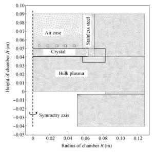
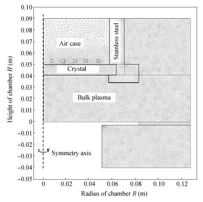
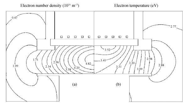
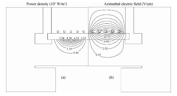
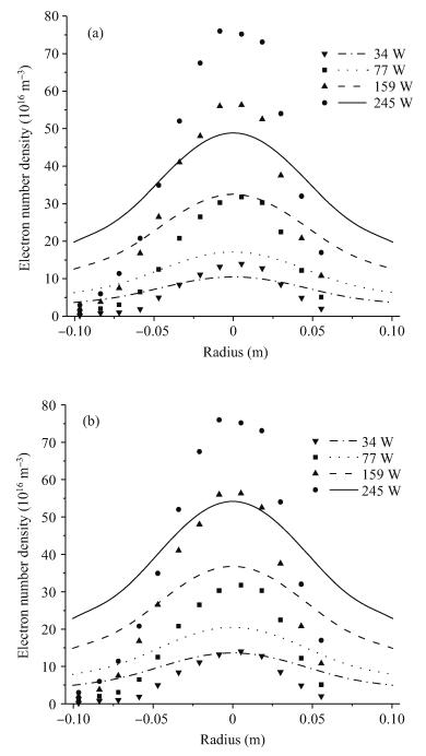
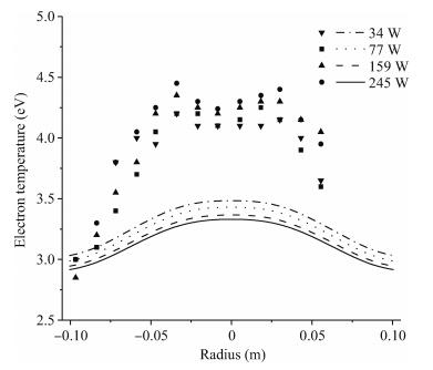
A two-dimensional axisymmetric inductively coupled plasma (ICP) model, and its implementation in the COMSOL multiphysical software, is described. The simulations are compared with the experimental results of argon discharge from the gaseous electronics conference RF reference cell in the inductively coupled plasma mode. The general trends of the number density and temperature of electrons with radial scanning are approximately correct. Finally, we discuss the reasons why the comparisons are not in agreement, and then propose an improvement in the assumptions of the Maxwellian electron energy distribution function and reaction rate.
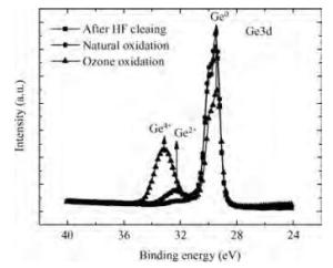
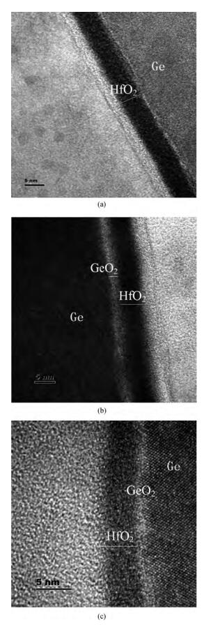
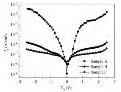
The physical and electrical properties of a Ge/GeO2/HfO2/Al gate stack are investigated. A thin interfacial GeO2 layer (~1 nm) is formed between Ge and HfO2 by dual ozone treatments, which passivates the Ge/high-k interface. Capacitors on p-type Ge substrates show very promising capacitance-voltage (C-V) characteristics by using in situ pre-gate ozone passivation and ozone ambient annealing after high-k deposition, indicating efficient passivation of the Ge/HfO2 interface. It is shown that the mid-gap interface state density at the Ge/GeO2 interface is 6.4×1011 cm-2·eV-1. In addition, the gate leakage current density of the Ge/GeO2/HfO2/Al gate stack passivated by the dual ozone treatments is reduced by about three orders of magnitude compared to that of a Ge/HfO2/Al gate stack without interface passivation.