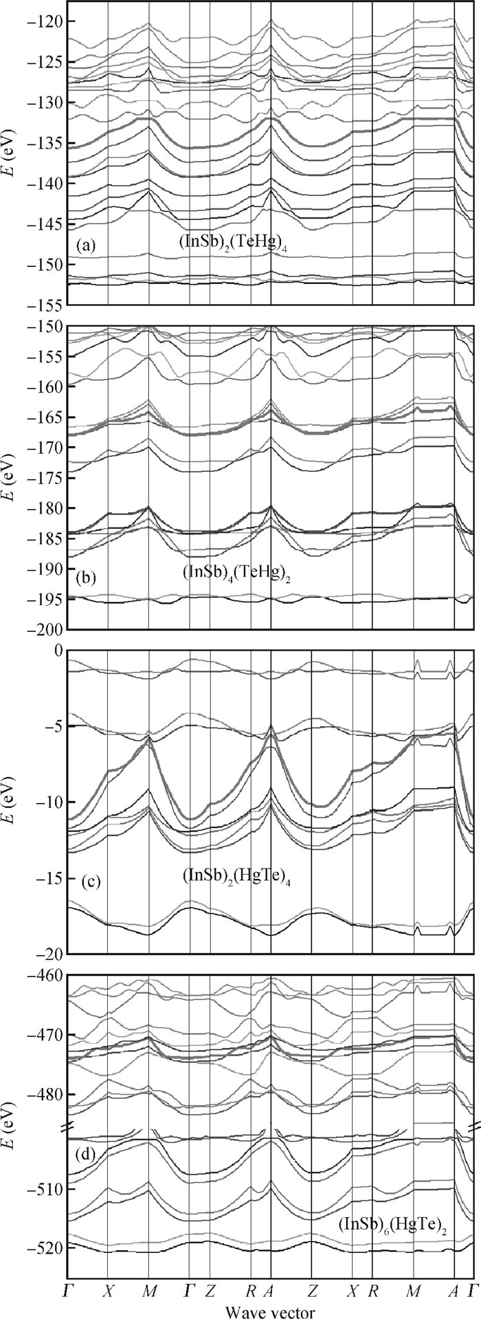
The electronic structure of (InSb)m/(HgTe)n short period superlattices grown along the (001) direction is studied theoretically using norm-conserving pseudo-potentials together with the local-density approximation for the exchange-correlation potential. The band structure depends on the value of m and n, the number of mono-layers and on the ordering of atoms at the InSb/HgTe interface in one unit cell. Our calculation indicates that the superlattice can be a semiconductor having a band gap between the occupied and unoccupied bands, or a metal with no band gap at the Fermi energy.According to the further calculation of total charge density between (InSb)m/(HgTe)n with different structures, a clearly different behavior happens when the structure changes from a system with a gap and a system without a gap.


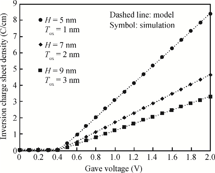
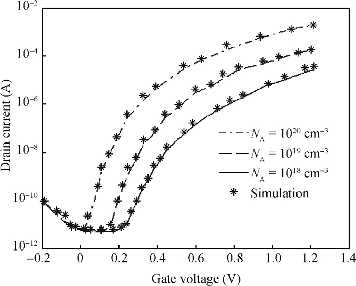
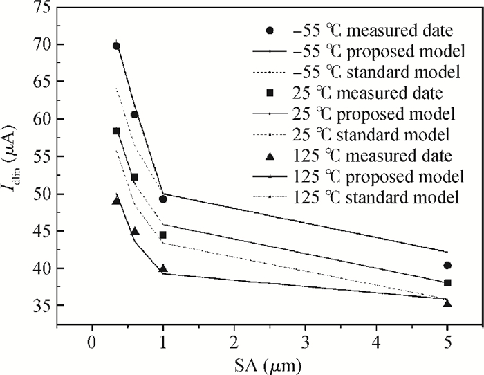
A physical and explicit surface potential model for undoped symmetric double-gate polysilicon thin-film transistors has been derived based on an effective charge density approach of Poisson's equation with both exponential deep and tail state terms included. The proposed surface potential calculation is single-piece and eliminates the regional approach. Model predictions are compared to numerical simulations with close agreement, having absolute error in the millivolt range. Furthermore, expressions of the drain current are given for a wide range of operation regions, which have been justified by thorough comparisons with experimental data.


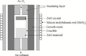
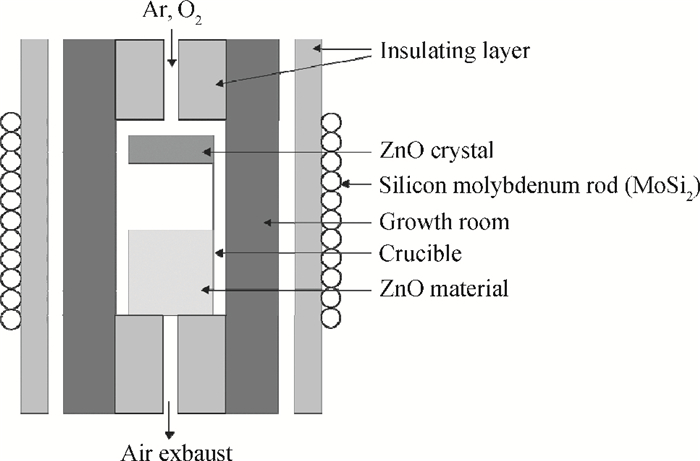
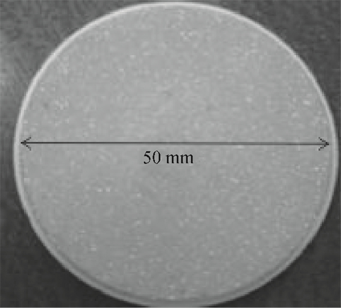
Zinc oxide (ZnO) has a wide band gap, high stability and a high thermal operating range that makes it a suitable material as a semiconductor for fabricating light emitting diodes (LEDs) and laser diodes, photodiodes, power diodes and other semiconductor devices. Recently, a new crystal growth for producing ZnO crystal boules was developed, which was physical vapor transport (PVT), at temperatures exceeding 1500℃ under a certain system pressure. ZnO crystal wafers in sizes up to 50 mm in diameter were produced. The conditions of ZnO crystal growth, growth rate and the quality of ZnO crystal were analyzed. Results from crystal growth and material characterization are presented and discussed. Our research results suggest that the novel crystal growth technique is a viable production technique for producing ZnO crystals and substrates for semiconductor device applications.


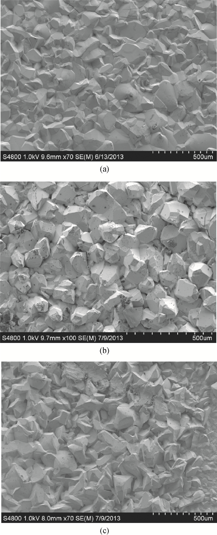
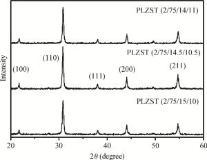
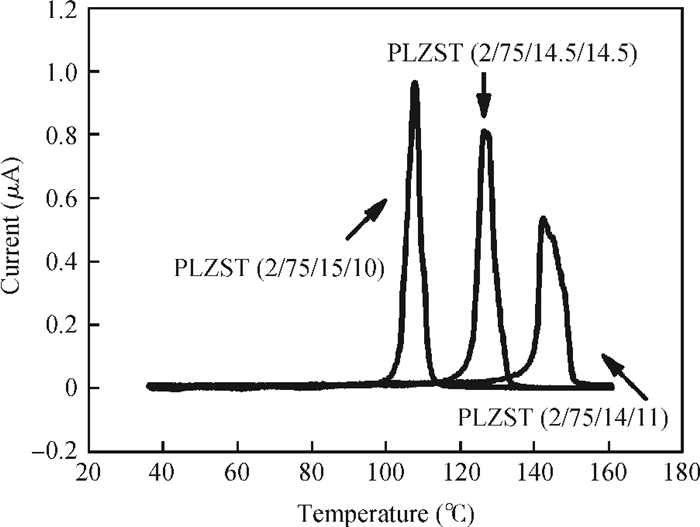
Pb0.97La0.02(Zr0.75Sn0.25-xTix)O3 (x=0.10, 0.105, 0.11) (PLZST) antiferroelectric ceramics with highly preferred-(110) orientation were successfully fabricated via the conventional solid-state reaction method. The antiferroelectric nature of PLZST ceramics induced by electric field was demonstrated by the dielectric constant-temperature (D-T) and the polarization-electric field (P-E) measurement. Typical phase transition from ferroelectric (FE) to antiferroelectric (AFE), and then to paraelectric (PE) is obtained. The results indicate that the phase transition behavior is suppressed with increasing of x, and Tc is remarkably shifted to higher temperature of 168℃, 170℃ and 174℃, respectively. Besides, high phase transition current (1×10⁻⁶ A, 8×10⁻⁷ A and 6×10⁻⁷ A, respectively) is obtained with temperature induced. Consequently, the excellent electric properties and the restraint between temperature and electric field would provide basis on the application of PLZST antiferroelectric ceramics in microelectronic integrated systems and sophisticated weapons systems.


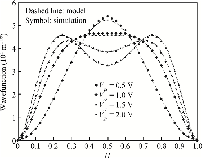
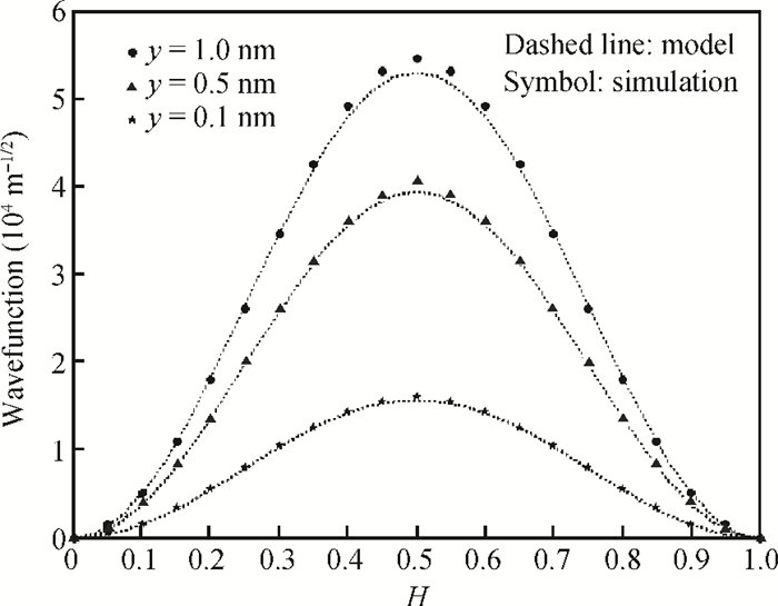
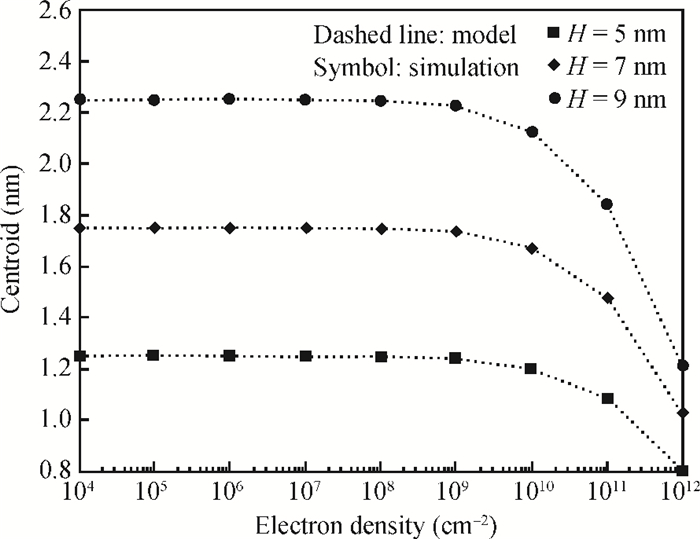
Quantum effects are predominant in tri-gate MOSFETs, so a model should be developed. For the first time, this paper presents the analytical model for quantization effects of thin film silicon tri-gate MOSFETs by using variational approach. An analytical expression of the inversion charge distribution function (ICDF) or wave function for the tri-gate MOSFETs has been obtained. This obtained ICDF is used to calculate the important device parameters, such as the inversion charge centroid and inversion charge density. The results are validated against with the simulation data.


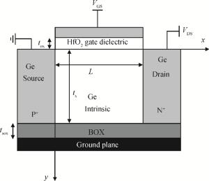
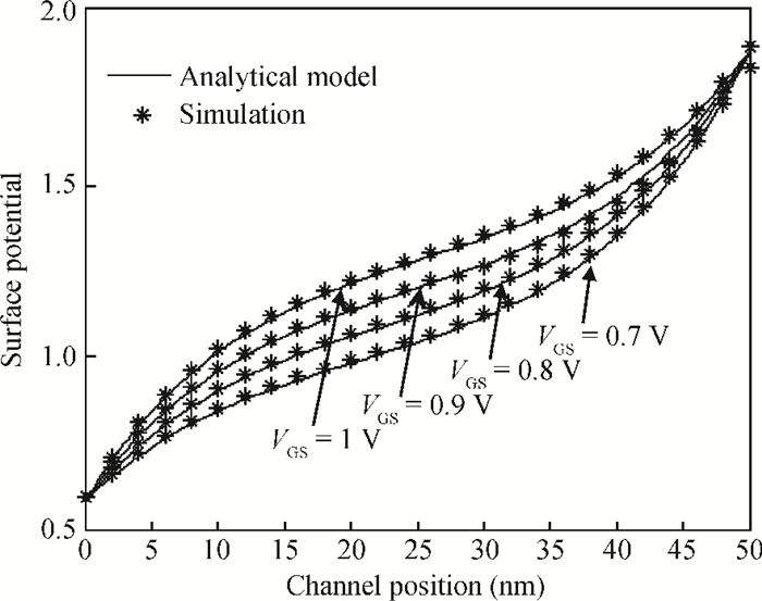
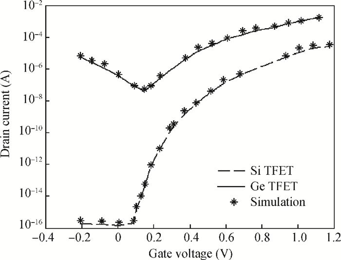
This paper proposes a new two dimensional (2D) analytical model for a germanium (Ge) single gate silicon-on-insulator tunnel field effect transistor (SG SOI TFET). The parabolic approximation technique is used to solve the 2D Poisson equation with suitable boundary conditions and analytical expressions are derived for the surface potential, the electric field along the channel and the vertical electric field. The device output tunnelling current is derived further by using the electric fields. The results show that Ge based TFETs have significant improvements in on-current characteristics. The effectiveness of the proposed model has been verified by comparing the analytical model results with the technology computer aided design (TCAD) simulation results and also comparing them with results from a silicon based TFET.


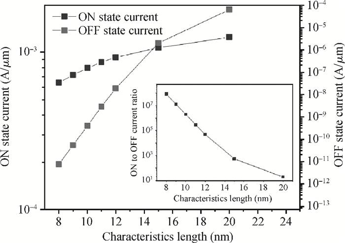
This paper proposes a laterally graded junctionless transistor taking peak doping concentration near the source and drain region, and a gradual decrease in doping concentration towards the center of the channel to improve the IOFF and ION/IOFF ratio. The decrease of doping concentration in the lateral direction of the channel region depletes a greater number of charge carriers compared to the uniformly doped channel in the OFF-state, which in turn suppresses the OFF state current flowing through the device without greatly affecting the ON state current.


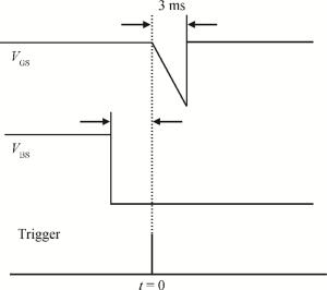
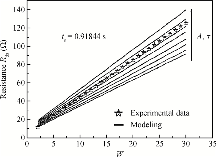
This study focuses on modeling the effects of deep hole traps, mainly the effect of the substrate (backgating effect) in a GaAs transistor MESFT. This effect is explained by the existence, at the interface, of a space charge zone. Any modulation in this area leads to response levels trapping the holes therein to the operating temperature. We subsequently developed a model treating the channel substrate interface as an N-P junction, allowing us to deduce the time dependence of the component parameters of the total resistance Rds, the pinch-off voltage VP, channel resistance, fully open Rco and the parasitic series resistance RS to bind the effect trap holes H1 and H0. When compared with the experimental results, the values of the RDS (tS) model for both traps show that there is an agreement between theory and experiment; it has inferred parameter traps, namely the density and the time constant of the trap. This means that a space charge region exists at the channel-substrate interface and that the properties can be approximated to an N-P junction.


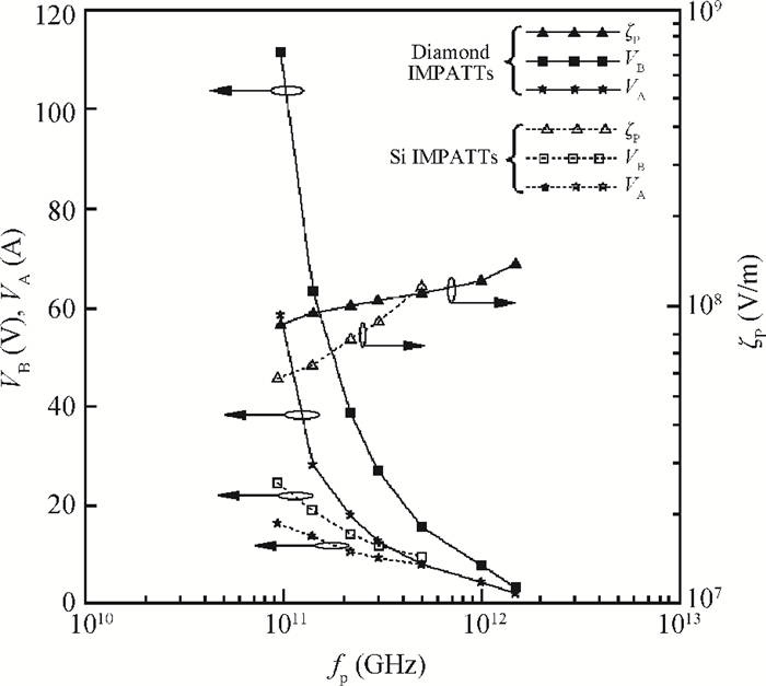
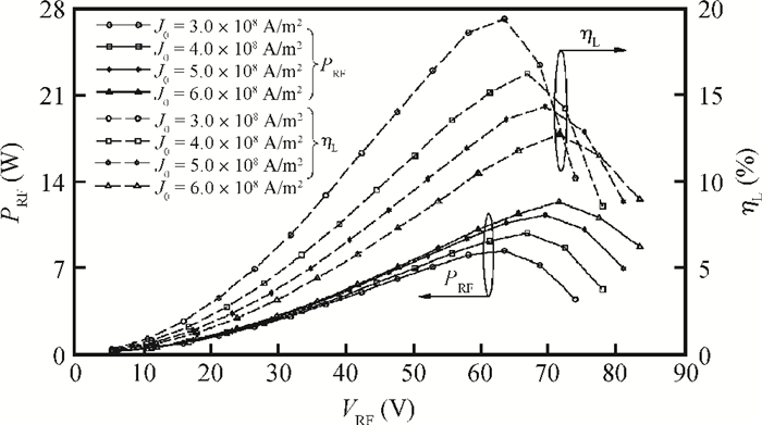
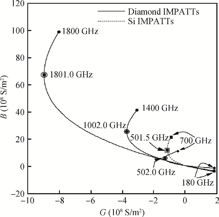
An attempt is made in this paper to explore the potentiality of semiconducting type-Ⅱb diamond as the base material of double-drift region (DDR) impact avalanche transit time (IMPATT) devices operating at both millimetre-wave (mm-wave) and terahertz (THz) frequencies. A rigorous large-signal (L-S) simulation based on the non-sinusoidal voltage excitation (NSVE) model developed earlier by the authors is used in this study. At first, a simulation study based on avalanche response time reveals that the upper cut-off frequency for DDR diamond IMPATTs is 1.5 THz, while the same for conventional DDR Si IMPATTs is much smaller, i.e. 0.5 THz. The L-S simulation results show that the DDR diamond IMPATT device delivers a peak RF power of 7.79 W with an 18.17% conversion efficiency at 94 GHz; while at 1.5 THz, the peak power output and conversion efficiency decrease to 6.19 mW and 8.17% respectively, taking 50% voltage modulation. A comparative study of DDR IMPATTs based on diamond and Si shows that the former excels over the later as regards high frequency and high power performance at both mm-wave and THz frequency bands. The effect of band to band tunneling on the L-S properties of DDR diamond and Si IMPATTs has also been studied at different mm-wave and THz frequencies.


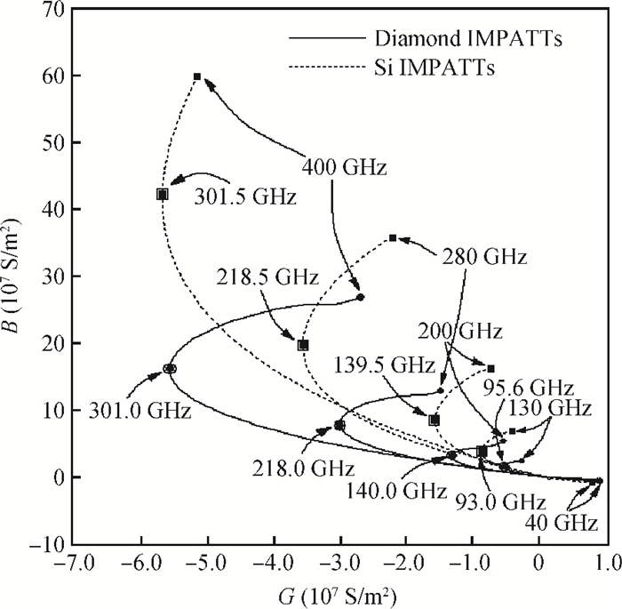


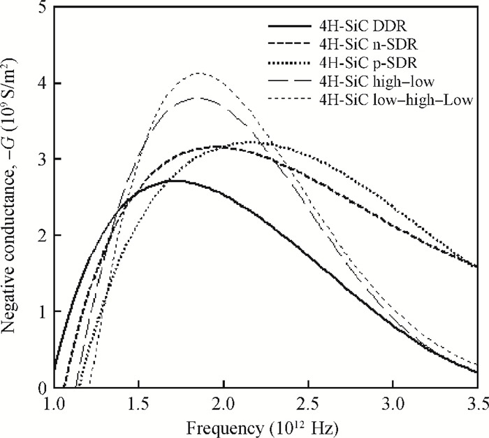
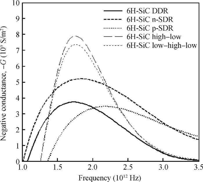
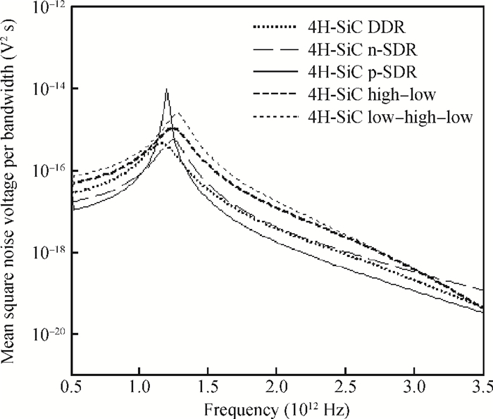
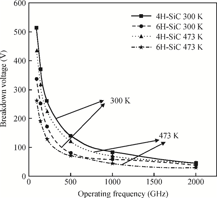
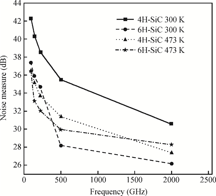
We have presented a comparative account of the high frequency prospective as well as noise behaviors of wide-bandgap 4H-SiC and 6H-SiC based on different structures of IMPATT diodes at sub-millimeter-wave frequencies up to 2.18 THz. The computer simulation study establishes the feasibility of the SiC based IMPATT diode as a high power density terahertz source. The most significant feature lies in the noise behavior of the SiC IMPATT diodes. It is noticed that the 6H-SiC DDR diode shows the least noise measure of 26.1 dB as compared to that of other structures. Further, it is noticed that the noise measure of the SiC IMPATT diode is less at a higher operating frequency compared to that at a lower operating frequency.


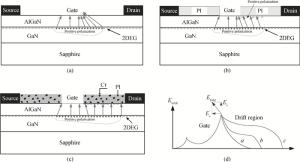
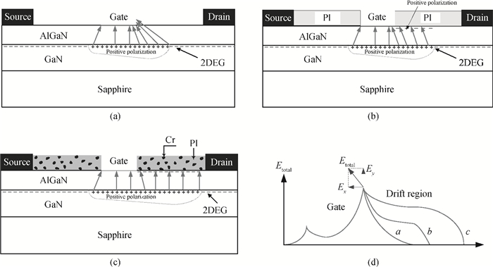
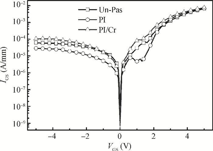
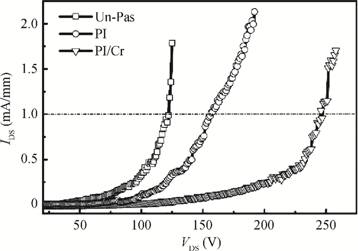
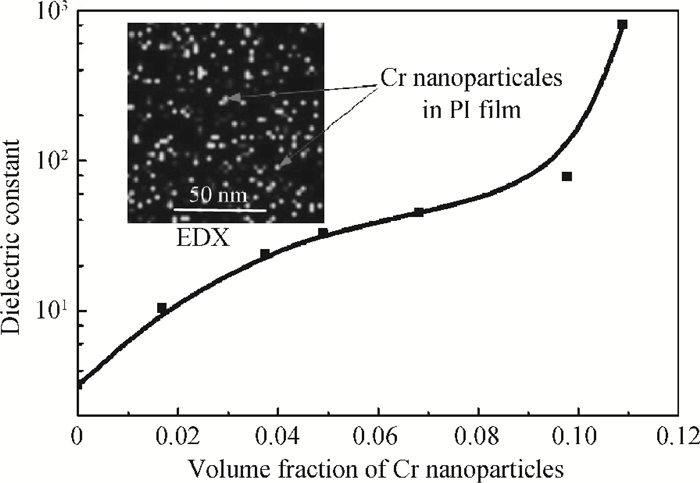
A novel AlGaN/GaN high electric mobility transistor (HEMT) with polyimide (PI)/chromium (Cr) as the passivation layer is proposed for enhancing breakdown voltage and its DC performance is also investigated. The Cr nanoparticles firstly introduced in PI thin films by the co-evaporation can be used to increase the permittivity of PI film. The high-permittivity PI/Cr passivation acting as field plate can suppress the fringing electric field peak at the drain-side edge of the gate electrode. This mechanism is demonstrated in accord with measured results. The experimental results show that in comparison with the AlGaN/GaN HEMTs without passivation, the breakdown voltage of HEMTs with the PI/Cr composite thin films can be significantly improved, from 122 to 248 V.


The STI stress effect is investigated based on the 0.13 μm SOI process developed by the Institute of Microelectronics of the Chinese Academy of Sciences (IMECAS). It shows that the threshold voltage and mobility are all affected by the STI stress. The absolute value of the threshold voltage of NMOS and PMOS increased by about 10%, the saturation current of NMOS decreases by about 20%, while the saturation current of PMOS increases by about 20%. It is also found that the lower temperature enhances the STI stress and then influences the device performance further. Then a macro model for this effect is proposed and is well verified.


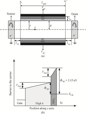
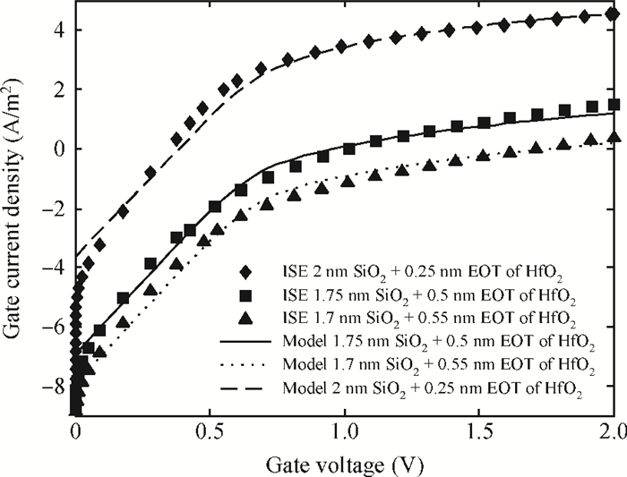
An analytical direct tunneling gate current model for cylindrical surrounding gate (CSG) MOSFETs with high-k gate stacks is developed. It is found that the direct tunneling gate current is a strong function of the gate's oxide thickness, but that it is less affected by the change in channel radius. It is also revealed that when the thickness of the equivalent oxide is constant, the thinner the first layer, the smaller the direct tunneling gate current. Moreover, it can be seen that the dielectric with a higher dielectric constant shows a lower tunneling current than expected. The accuracy of the analytical model is verified by the good agreement of its results with those obtained by the three-dimensional numerical device simulator ISE.


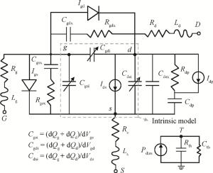
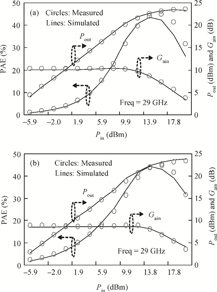
A complete and accurate surface potential based large-signal model for compound semiconductor HEMTs is presented. A surface potential equation resembling the one used in conventional MOSFET models is achieved. The analytic solutions from the traditional surface potential theory that developed in MOSFET models are inherited. For core model derivation, a novel method is used to realize a direct application of the standard surface potential model of MOSFETs for HEMT modeling, without breaking the mathematic structure. The high-order derivatives of I-V/C-V remain continuous, making the model suitable for RF large-signal applications. Furthermore, the self-heating effects and the transconductance dispersion are also modelled. The model has been verified through comparison with measured DC Ⅳ, Gummel symmetry test, CV, minimum noise figure, small-signal S-parameters up to 66 GHz and single-tone input power sweep at 29 GHz for a 4×75 μm×0.1 μm InGaAs/GaAs power pHEMT, fabricated at a commercial foundry.


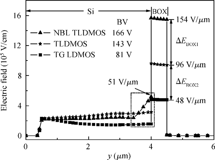
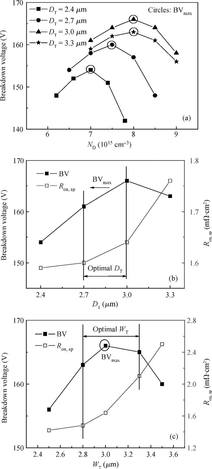
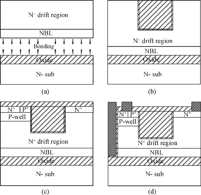
A low specific on-resistance (Ron, sp) SOI NBL TLDMOS (silicon-on-insulator trench LDMOS with an N buried layer) is proposed. It has three features:a thin N buried layer (NBL) on the interface of the SOI layer/buried oxide (BOX) layer, an oxide trench in the drift region, and a trench gate extended to the BOX layer. First, on the on-state, the electron accumulation layer forms beside the extended trench gate; the accumulation layer and the highly doping NBL constitute an L-shaped low-resistance conduction path, which sharply decreases the Ron, sp. Second, in the y-direction, the BOX's electric field (E-field) strength is increased to 154 V/μm from 48 V/μm of the SOI Trench Gate LDMOS (SOI TG LDMOS) owing to the high doping NBL. Third, the oxide trench increases the lateral E-field strength due to the lower permittivity of oxide than that of Si and strengthens the multiple-directional depletion effect. Fourth, the oxide trench folds the drift region along the y-direction and thus reduces the cell pitch. Therefore, the SOI NBL TLDMOS structure not only increases the breakdown voltage (BV), but also reduces the cell pitch and Ron, sp. Compared with the TG LDMOS, the NBL TLDMOS improves the BV by 105% at the same cell pitch of 6 μm, and decreases the Ron, sp by 80% at the same BV.


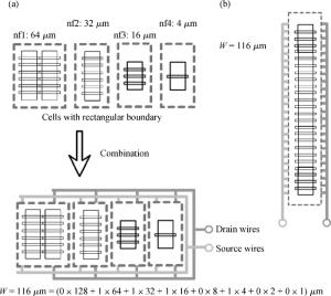
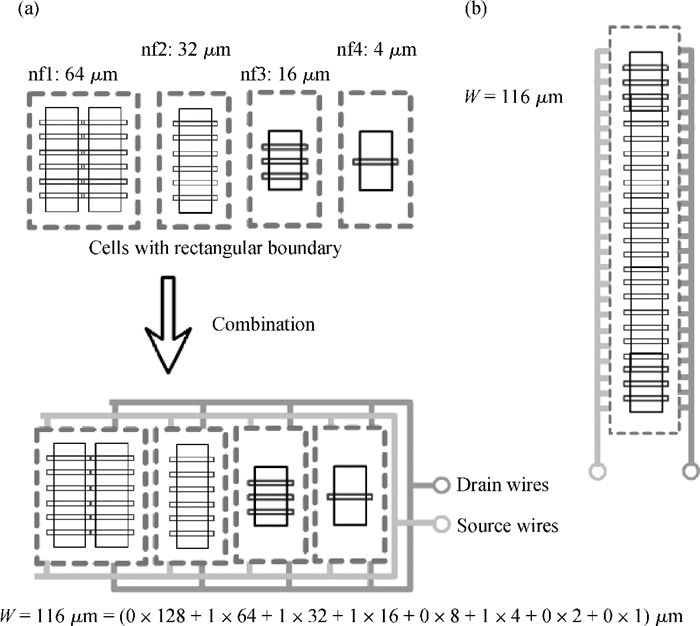
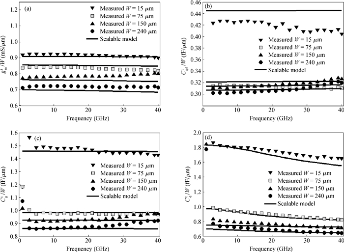
This work presents a highly efficient approach for broadband modeling of millimeter-wave CMOS FETs with gate width scalability by using pre-modeled cells. Only a few devices with varied gate width are required to be measured and modeled with fixed models, and later used as pre-modeled cells. Then a target device with the desired gate width is constructed by choosing appropriate cells and connecting them with a wiring network. The corresponding scalable model is constructed by incorporating the fixed models of the cells used in the target device and the scalable model of the connection wires. The proposed approach is validated by experiments on 65-nm CMOS process up to 40 GHz and across a wide range of gate widths.


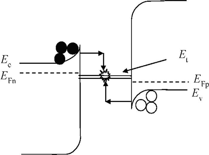
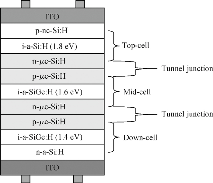
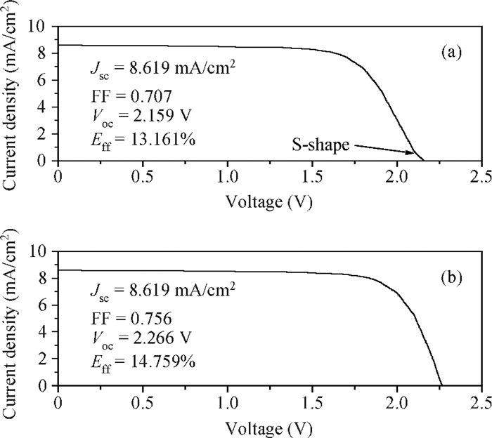
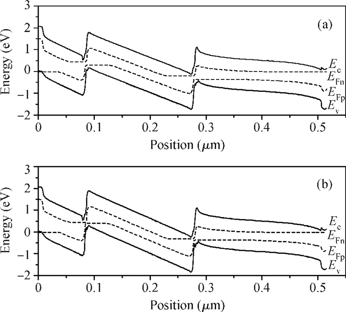
The computer program AMPS-1D (analysis of microelectronic and photonic structures) has been employed to simulate the performance of the a-Si:H/a-SiGe:H/a-SiGe:H triple-junction solar cell at the radiation of AM1.5G (100 mW/cm2) and room temperature. Firstly, three sub-cells with band gaps of 1.8, 1.6 and 1.4 eV are simulated, respectively. The simulation results indicate that the density of defect states is an important factor, which affects the open circuit voltage and the filling factor of the solar cell. The two-step current matching method and the control variate method are employed in the simulation. The results show that the best solar cell performance would be achieved when the intrinsic layer thickness from top to bottom is set to be 70, 180 and 220 nm, respectively. We also optimize the tunnel-junction structure of the solar cell reasonably, the simulation results show that the open circuit voltage, filling factor and conversion efficiency are all improved and the S-shape current density-voltage curve disappears during optimizing the tunnel-junction structure. Besides, the diagram of the energy band and the carrier recombination rate are also analyzed. Finally, our simulation data are compared to the experimental data published in other literature. It is demonstrated that the numerical results agree with the experimental ones very well.


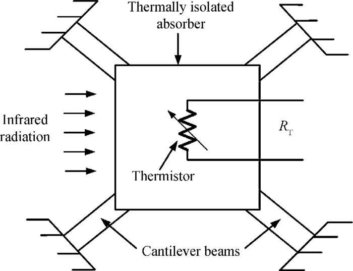
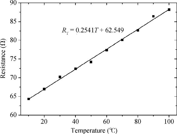
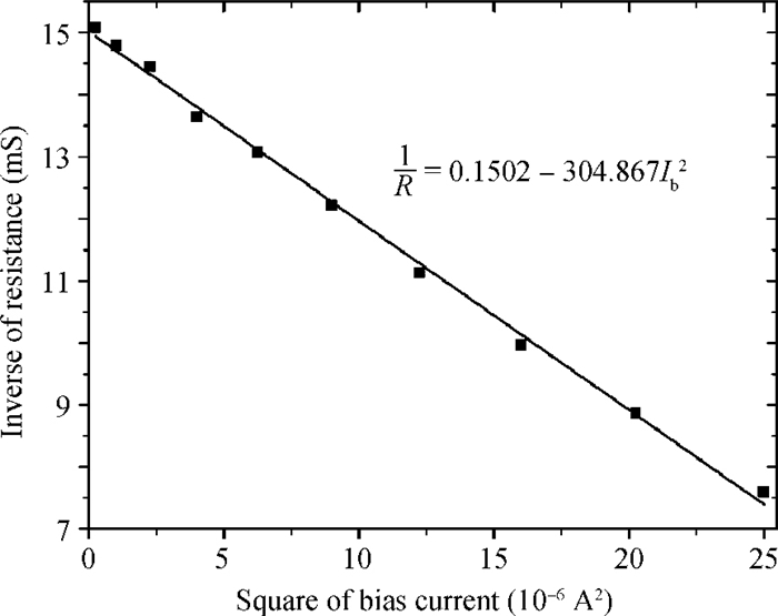
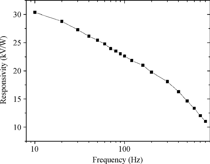
This paper introduces a low-cost infrared absorbing structure for an uncooled infrared detector in a standard 0.5 μm CMOS technology and post-CMOS process. The infrared absorbing structure can be created by etching the surface sacrificial layer after the CMOS fabrication, without any additional lithography and deposition procedures. An uncooled infrared microbolometer is fabricated with the proposed infrared absorbing structure. The microbolometer has a size of 65×65 μm2 and a fill factor of 37.8%. The thermal conductance of the microbolometer is calculated as 1.33×10⁻⁵ W/K from the measured response to different heating currents. The fabricated microbolometer is irradiated by an infrared laser, which is modulated by a mechanical chopper in a frequency range of 10-800 Hz. Measurements show that the thermal time constant is 0.995 ms and the thermal mass is 1.32×10⁻⁸ J/K. The responsivity of the microbolometer is about 3.03×10⁴ V/W at 10 Hz and the calculated detectivity is 1.4×108 cm·Hz1/2/W.


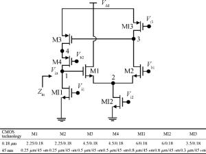
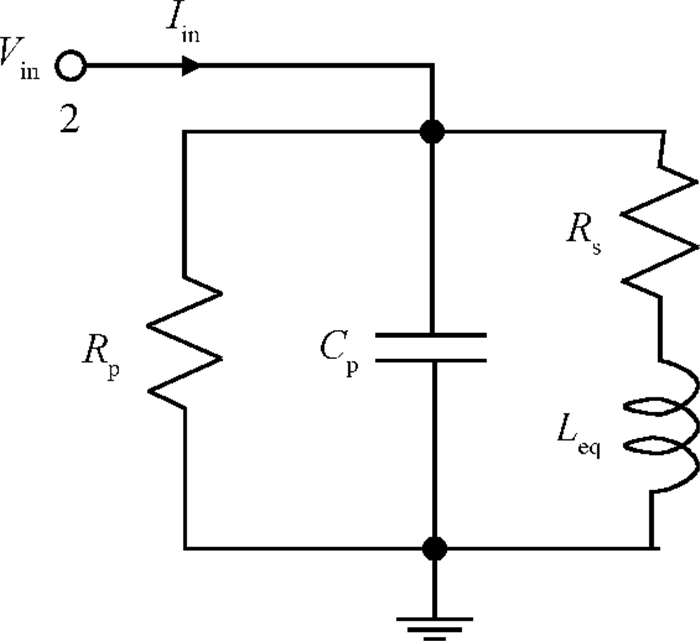
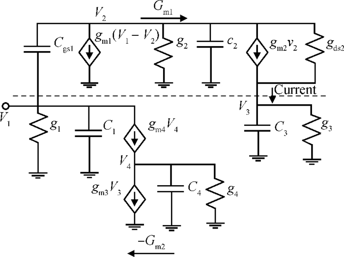
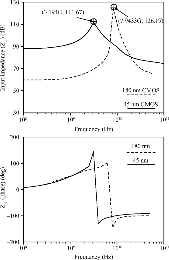
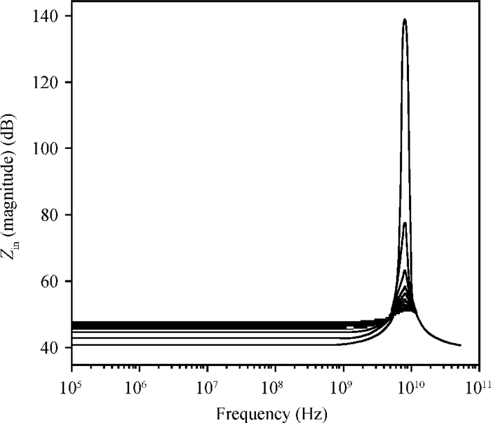
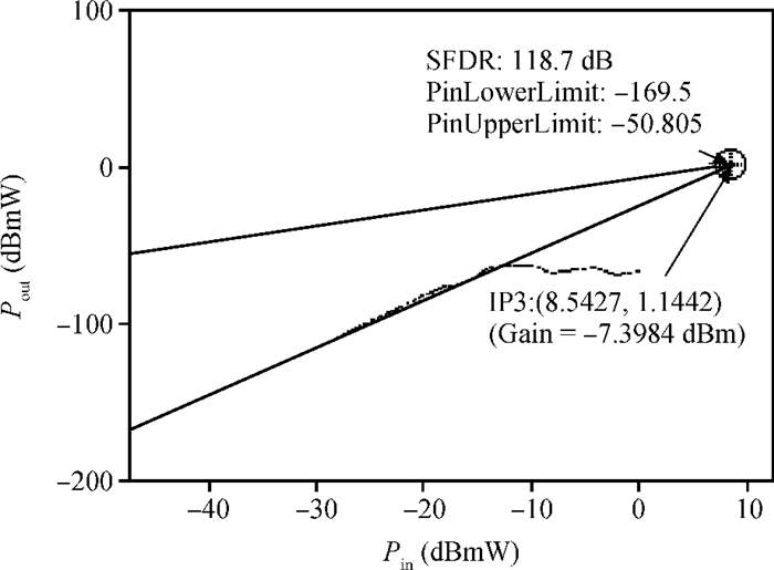
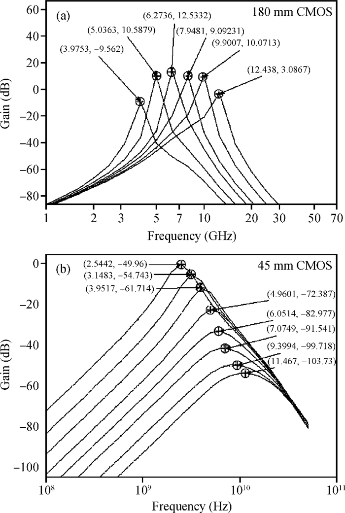
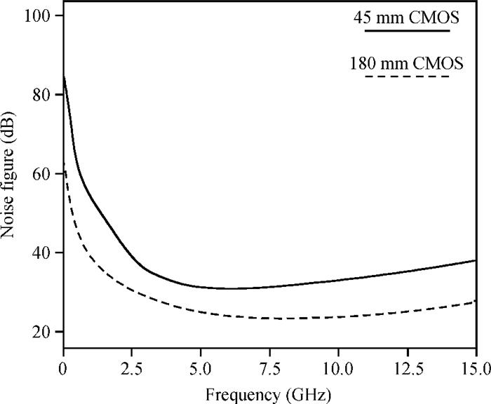
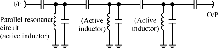
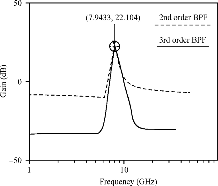
This paper presents a low power tunable active inductor and RF band pass filter suitable for multiband RF front end circuits. The active inductor circuit uses the PMOS cascode structure as the negative transconductor of a gyrator to reduce the noise voltage. Also, this structure provides possible negative resistance to reduce the inductor loss with wide inductive bandwidth and high resonance frequency. The RF band pass filter is realized using the proposed active inductor with suitable input and output buffer stages. The tuning of the center frequency for multiband operation is achieved through the controllable current source. The designed active inductor and RF band pass filter are simulated in 180 nm and 45 nm CMOS process using the Synopsys HSPICE simulation tool and their performances are compared. The parameters, such as resonance frequency, tuning capability, noise and power dissipation, are analyzed for these CMOS technologies and discussed. The design of a third order band pass filter using an active inductor is also presented.


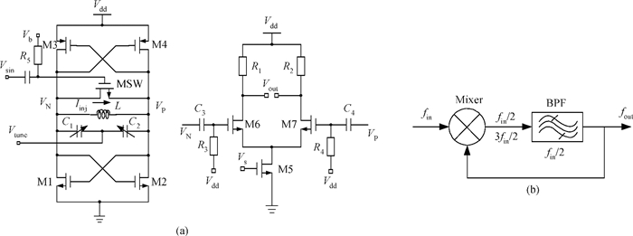
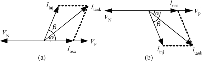
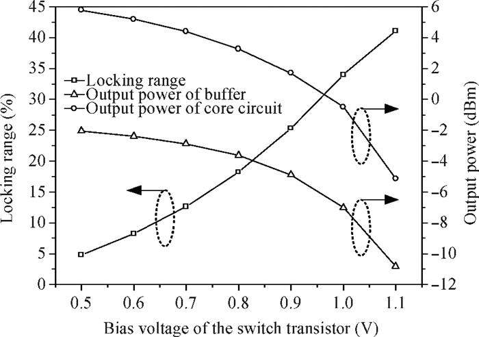
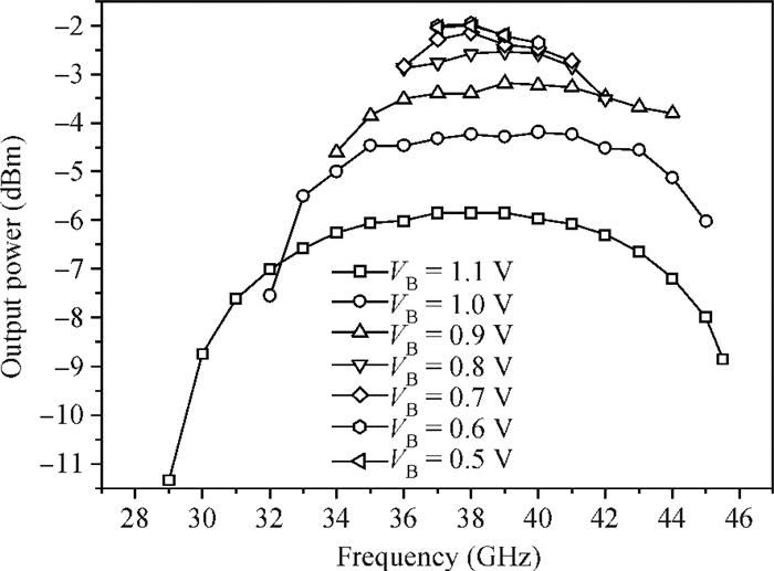
This paper proposes a direct injection-locked frequency divider (ILFD) with a wide locking range in the Ka-band. A complementary cross-coupled architecture is used to enhance the overdriving voltage of the switch transistor so that the divider locking range is extended efficiently. New insights into the locking range and output power are proposed. A new method to analyze and optimize the injection sensitivity is presented and a layout technique to reduce the parasitics of the cross-coupled transistors is applied to decrease the frequency shift and the locking range degradation. The circuit is designed in a standard 90-nm CMOS process. The total locking range of the ILFD is 43.8% at 34.5 GHz with an incident power of -3.5 dBm. The divider IC consumes 3.6 mW of power at the supply voltage of 1.2 V. The chip area including the pads is 0.5×0.5 mm2.


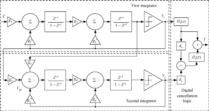
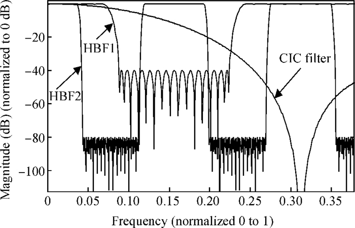
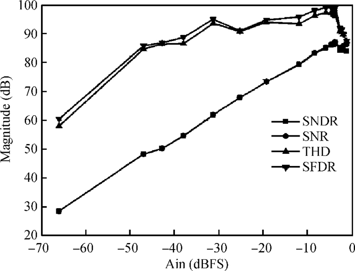
A single die 1.2 V multi-stage noise shaping (Mash) 2-2 delta sigma analog to digital converter (ADC) for wide applications is implemented. The configurable Mash 2-2 modulator with a new decimation filter design is presented to achieve wide and high dynamic range (DR) for multiple practical applications. The novel modulator can be configured as a Mash 2-2 modulator for high precision or a 2-order modulator for low DR. The decimation filter is designed to select the OSR flexibly among cascaded integrator comb (CIC) filter and two half-band filters (HBF). The serial peripheral interface (SPI) can be used to adjust the sampling frequency and the oversampling ratio (OSR). The design was fabricated in a 0.13 μm CMOS process with an area of 0.91 mm2 and a total power of 5.2 mW. The measurement results show that the dynamic range (DR) of the proposed ADC can change from 55 to 95 dB with the configurable OSR from 16 to 256. The spurious free dynamic range (SFDR) and signal-to-noise distortion ratio (SNDR) can get 99 dB and 86.5 dB, respectively.


A broadband programmable gain amplifier (PGA) with a small gain step and low gain error has been designed in 0.13 μm CMOS technology. The PGA was implemented with open-loop architecture to provide wide bandwidth. A two-stage gain control method, which consists of a resistor ladder attenuator and an active fine gain control stage, provides the small gain step. A look-up table based gain control method is introduced in the fine gain control stage to lower the gain error. The proposed PGA shows a decibel-linear variable gain from -4 to 20 dB with a gain step of 0.1 dB and a gain error less than ±0.05 dB. The 3-dB bandwidth and maximum ⅡP3 are 3.8 GHz and 17 dBm, respectively.


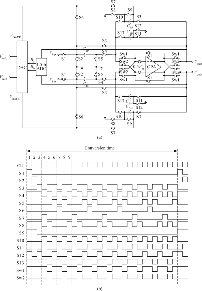
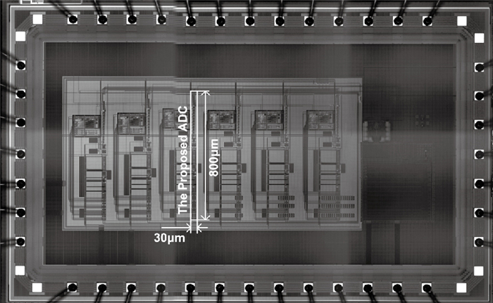
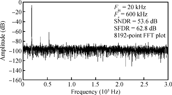
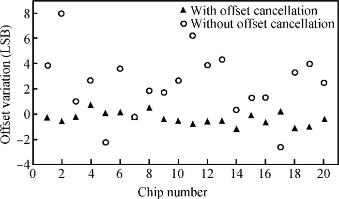
A 10-bit ratio-independent switch-capacitor (SC) cyclic analog-to-digital converter (ADC) with offset canceling for a CMOS image sensor is presented. The proposed ADC completes an N-bit conversion in 1.5N clock cycles with one operational amplifier. Combining ratio-independent and polarity swapping techniques, the conversion characteristic of the proposed cyclic ADC is inherently insensitive both to capacitor ratio and to amplifier offset voltage. Therefore, the circuit can be realized in a small die area and it is suitable to serve as the column-parallel ADC in CMOS image sensors. A prototype ADC is fabricated in 0.18-μm one-poly four-metal CMOS technology. The measured results indicate that the ADC has a signal-to-noise and distortion ratio (SNDR) of 53.6 dB and a DNL of +0.12/-0.14 LSB at a conversion rate of 600 kS/s. The standard deviation of the offset variation of the ADC is reduced from 2.5 LSB to 0.5 LSB. Its power dissipation is 250 μ W with a 1.8 V supply, and its area is 0.03×0.8 mm2.


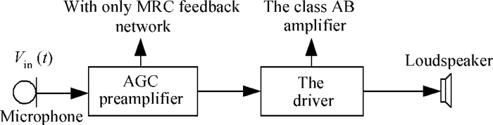
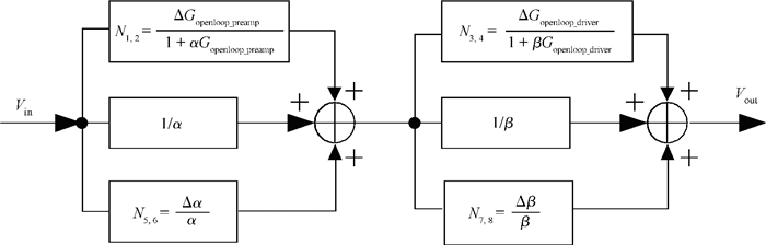
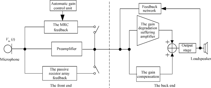
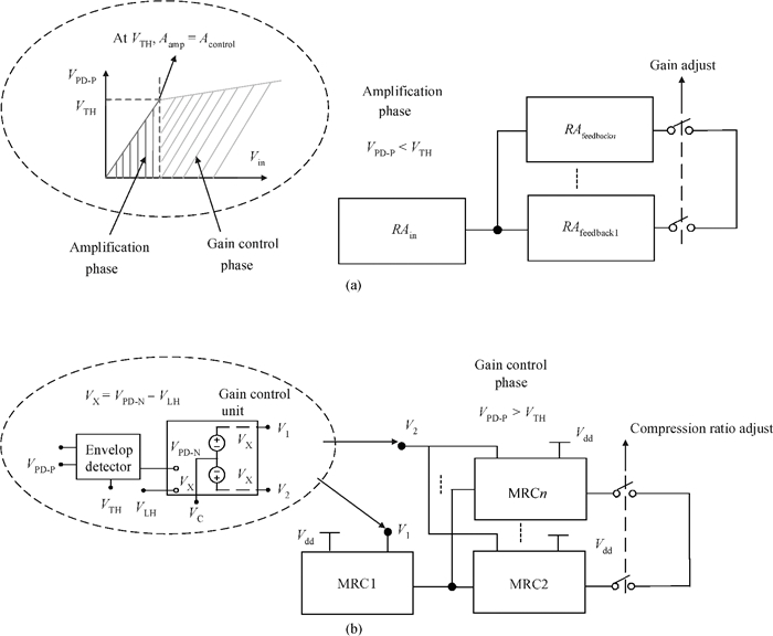
A hearing aid on-chip system based on accuracy optimized front-and back-end blocks is presented for enhancing the signal processing accuracy of the hearing aid. Compared with the conventional system, the accuracy optimized system is characterized by the dual feedback network and the gain compensation technique used in the front-and back-end blocks, respectively, so as to alleviate the nonlinearity distortion caused by the output swing. By using the technique, the accuracy of the whole hearing aid system can be significantly improved. The prototype chip has been designed with a 0.13 μm standard CMOS process and tested with 1 V supply voltage. The measurement results show that, for driving a 16 Ω loudspeaker with a normalized output level of 300 mVp-p, the total harmonic distortion reached about -60 dB, achieving at least three times reduction compared to the previously reported works. In addition, the typical input referred noise is only about 5 μ Vrms.


Conversion of the Reed-Muller (RM) expansion between two different polarities is an important step in the synthesis and optimization of RM circuits. By investigating XOR decomposition, a new conversion algorithm is proposed to convert MPRM expansion from one polarity to another. First, the relationship between XOR decomposition and mixed polarity is set up. Second, based on this, the operation relation of term coefficients between the two polarities is derived to realize MPRM expansion conversion. And finally, with the MCNC Benchmark, the results of our algorithm show that it is more suitable for dealing with MPRM expansion with more terms. Compared to the previous tabular technique, the conversion efficiency is improved up to approximately 44.39%.

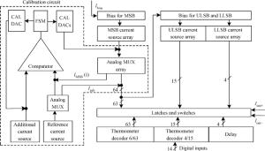
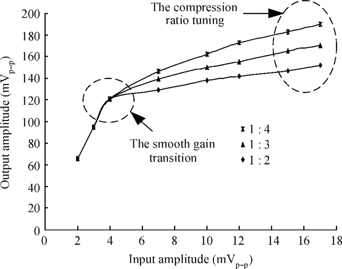
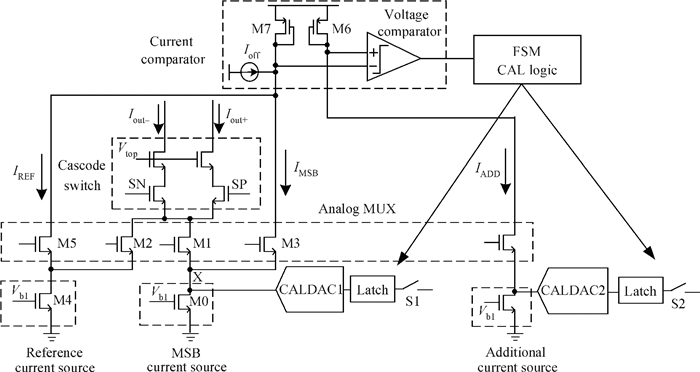
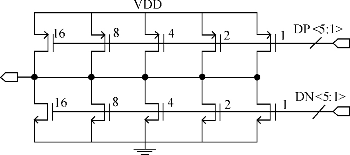
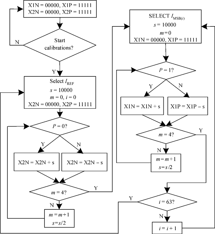
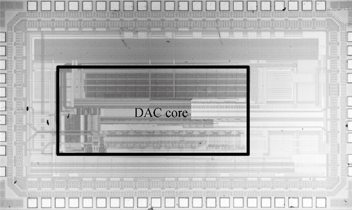
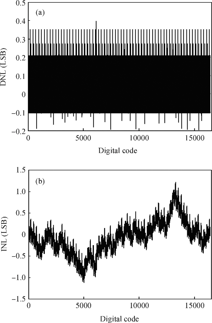
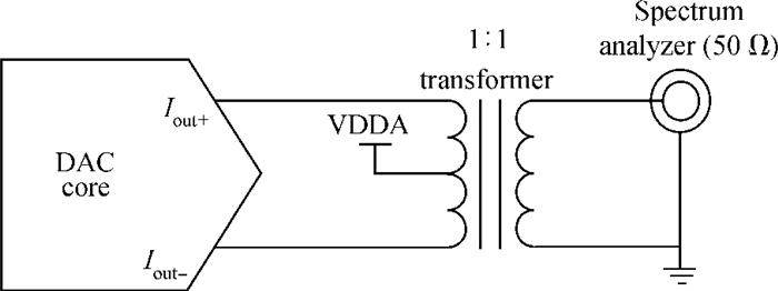
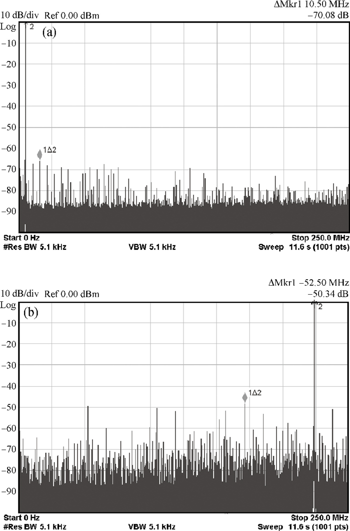
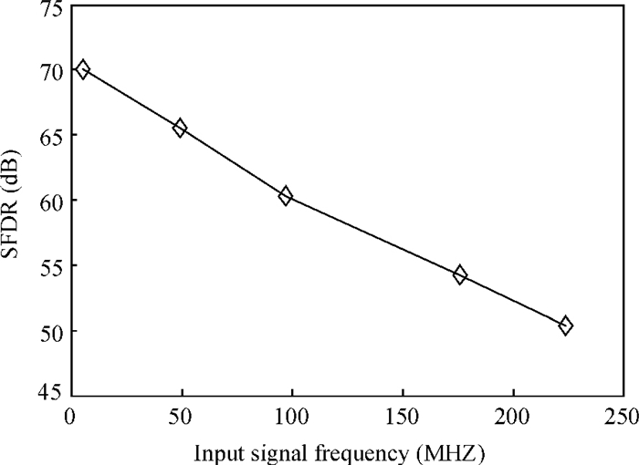
The linearity of current-steering digital-to-analog converters (DACs) at low signal frequencies is mainly limited by matching properties of current sources, so large-size current source arrays are widely used for better matching. This, however, results in large gradient errors and parasitic capacitance, which degrade the spurious free dynamic range (SFDR) for high-frequency signals. To overcome this problem, calibration is an effective method. In this paper, a digital background calibration technique for current-steering DACs is presented and verified by a 14-bit DAC in a 0.13 μm standard CMOS process. The measured differential nonlinearity (DNL) and integral nonlinearity (INL) are 0.4 LSB and 1.2 LSB, respectively. At 500-MS/s, the SFDR is 70 dB and 50.3 dB for signals of 5.4 MHz and 224 MHz, respectively. The core area is 0.69 mm2 and the power consumption is 165 mW from a mixed power supply with 1.2 V and 3.3 V.


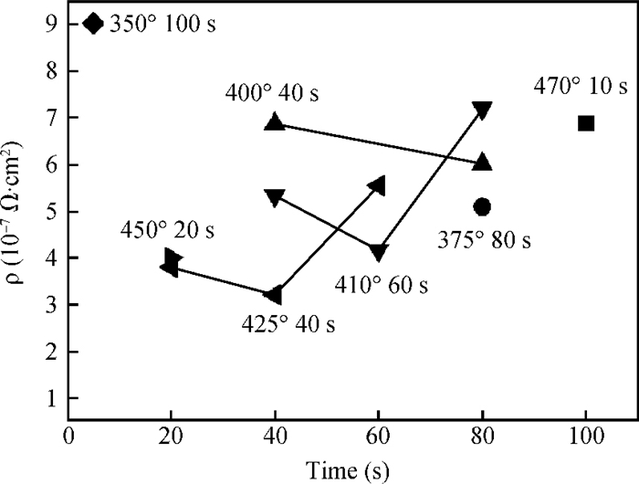
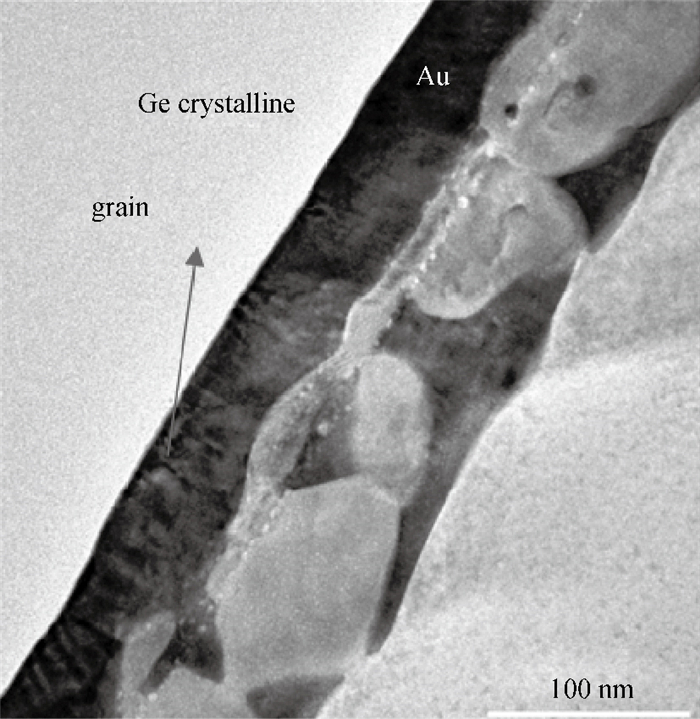
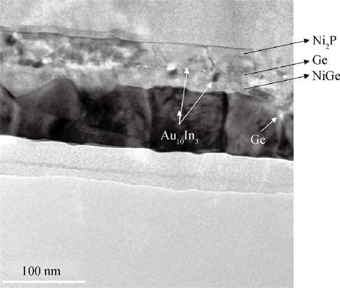
The effect of the annealing time and annealing temperature on Ni/Ge/Au electrode contacts deposited on the n-type InP contact layer has been studied using a circular transmission line model. The minimum specific contact resistance of 3.2×10⁻⁷Ω·cm2 was achieved on the low-doped n-type InP contact layer with a 40 s anneal at 425℃. In order to improve the ohmic contact and reduce the difficulty in the fabrication of the high doped InP epi-layer, the doping concentration in the InP contact layer was chosen to be 5×1018 cm-3 in the fabrication of transferred electronic devices. Excellent differential negative resistance properties were obtained by an electron beam evaporating the Ni/Ge/Au/Ge/Ni/Au composite electrode on an InP epi-layer with a 60 s anneal at 380℃.


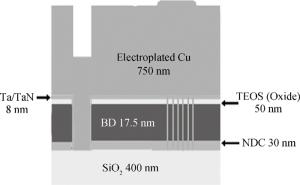
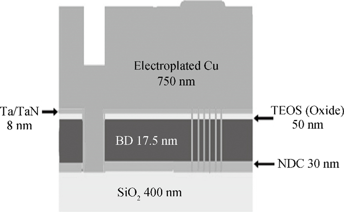
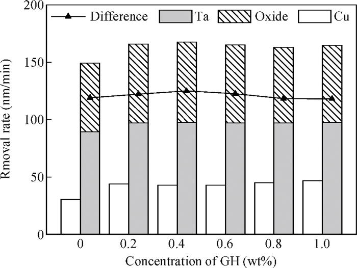
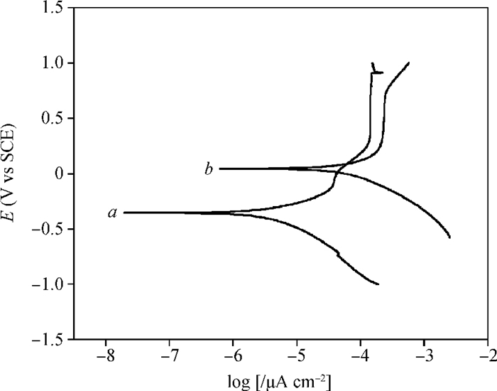
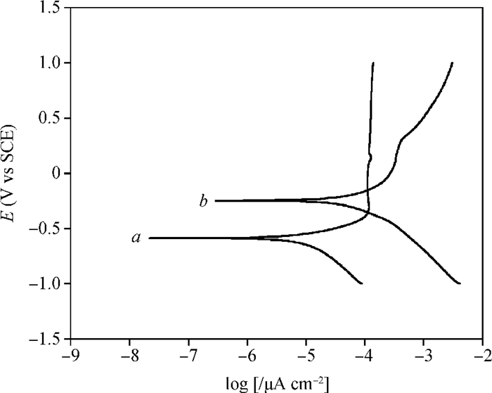
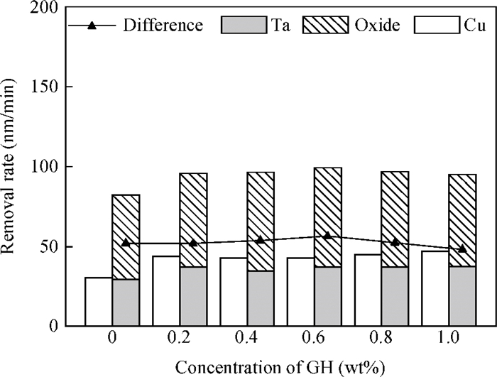
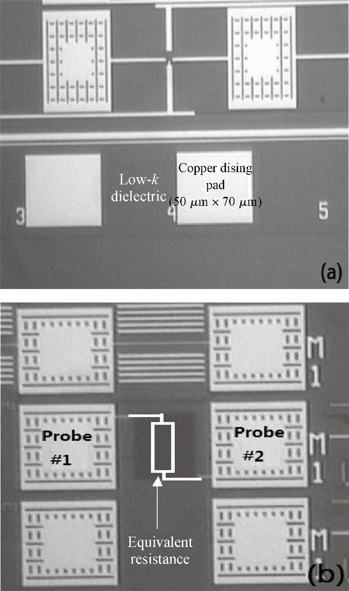
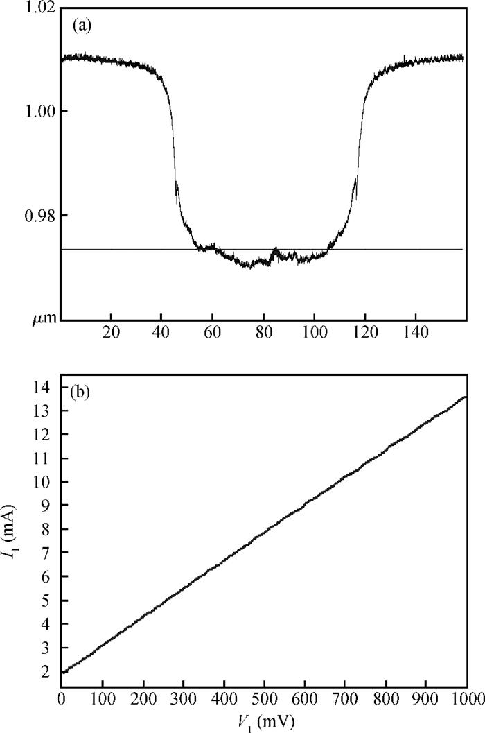
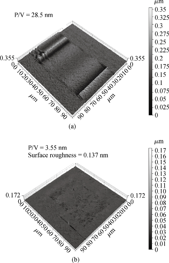
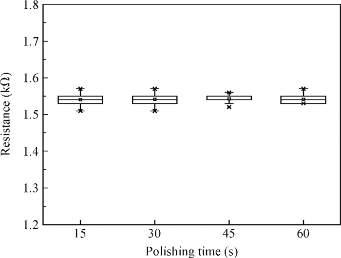
We propose an alkaline barrier slurry containing guanidine hydrochloride (GH) and hydrogen peroxide. The slurry does not contain any corrosion inhibitors, such as benzotriazole (BTA). 3-inch samples of tantalum copper and oxide were polished to observe the removal rate. The effect of GH on removal rate selectivity along with hydrogen peroxide was investigated by comparing slurry containing GH and H2O2 with slurry containing only GH. Details about the tantalum polishing mechanism in an alkaline guanidine-based slurry and the electrochemical reactions are discussed. The results show that guanidine hydrochloride can increase the tantalum polishing rate and the selectivity of copper and barrier materials. The variation of the dishing and wire line resistance with the polishing time was measured. The dishing value after a 300 mm pattern wafer polishing suggests that the slurry has an effective performance in topography modification. The result obtained from the copper wire line resistance test reveals that the wire line in the trench has a low copper loss.