Compared with microelectronic packaging, optoelectronic packaging as a new packaging type has been developed rapidly and it will play an essential role in optical communication.In this paper, we try to summarize the development history, research status, technology issues and future prospects, and hope to provide a meaningful reference.
Issue Browser
Volume 36, Issue 10,
Oct 2015

J. Semicond.
2015, 36(10): 102001 doi: 10.1088/1674-4926/36/10/102001

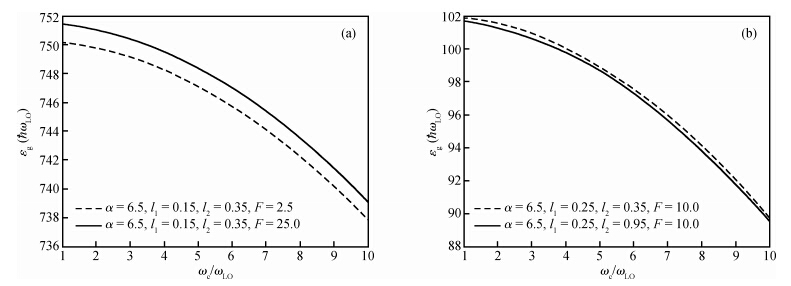
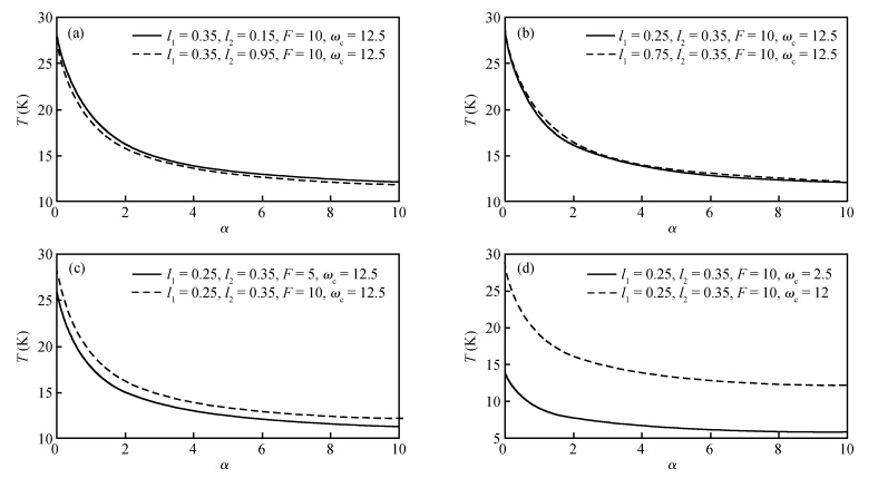
We investigate the influence of the electric field and magnetic fields on the ground state energy of a polaron in a spherical semiconductor quantum dot (QD) using the modified Lee Low Pines (LLP) method.The numerical results show the increase of the ground state energy with the increase of the electric field and the electron-phonon coupling constant, and the decrease with the magnetic field and the longitudinal confinement length.It is also seen that the temperature is an increasing function of the cyclotron frequency and the coupling constant whereas it decreases with the electric field strength.The modulation of the electric field, the magnetic field and the confinement length leads to the control of decoherence in the system.

J. Semicond.
2015, 36(10): 102002 doi: 10.1088/1674-4926/36/10/102002
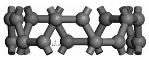
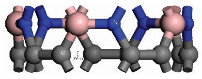
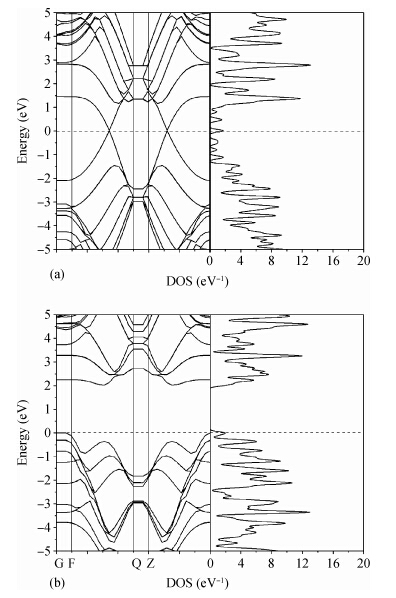
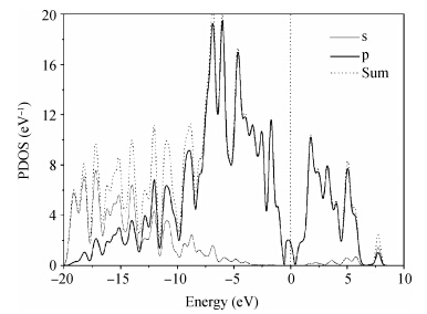
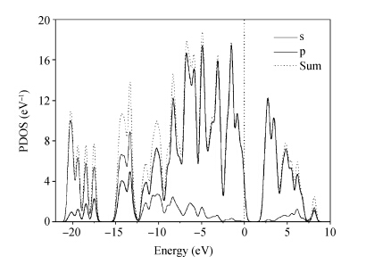
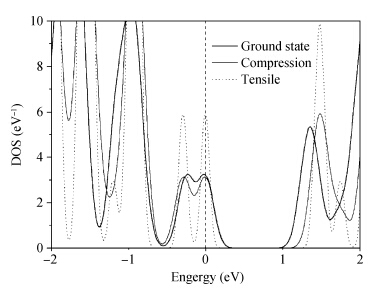
By using the CASTEP modules based on density functional theory, the electronic structures of B/N pair co-doping (5, 5) CNT rings superlattice have been investigated.The calculation results show that the formation energies of B/N pair co-doping CNT rings are negative, indicating that the new type construction will probably be stable.The band structure and state density of the new type construction show that the energy gap is opened by B/N co-doping in (5, 5) metallic CNT and the metallic CNT is changed into a semiconductor.The energy gap of pure CNT is strongly sensitive to the changes of CNT diameter but the energy gap of B/N co-doping CNT rings remains stable when the diameters are in a reasonable scope, which means that the requirements for the production of CNT have been reduced.The compressive deformation effects mean that the energy gaps are narrowed, which is equivalent to enhancing the doping volume concentration.However, the changes of the energy gap under the tensile deformation effect are opposite.Achieving control of the electrical conductivity of CNT has an important significance for electron devices.


J. Semicond.
2015, 36(10): 102003 doi: 10.1088/1674-4926/36/10/102003
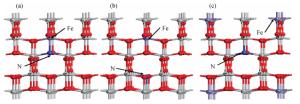
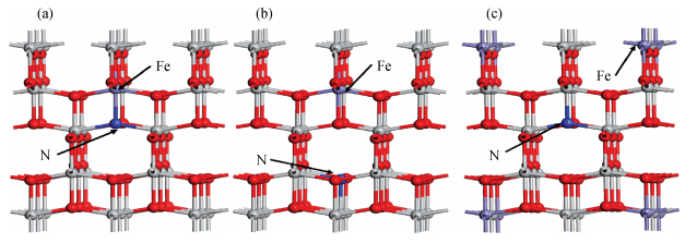
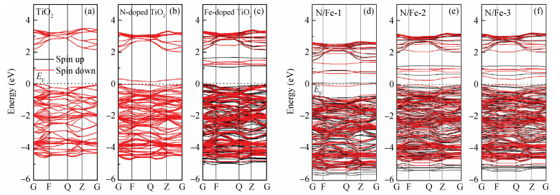
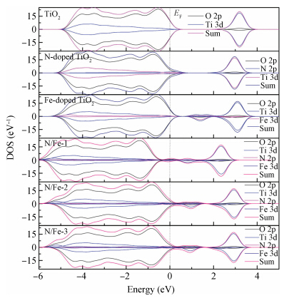
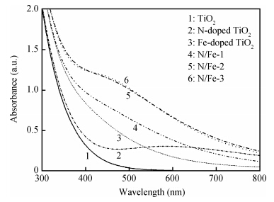
The electronic structure and optical properties of N and Fe codoping TiO2 have been investigated by first-principles calculations based on density functional theory.The calculated results indicate that the stability of N and Fe codoping TiO2 will change at different substitutional sites of N and Fe.The mechanism of band gap narrowing of doping TiO2 is discussed by investigating the density of state.The different substitutional site of N and Fe in codoping TiO2 influences the visible-light absorption.An increased visible-light absorption for doping TiO2 results from the synergistic effect of N and Fe codoping.Therefore, N and Fe codoping may enhance the visible-light photocatalytic activity of TiO2.
J. Semicond.
2015, 36(10): 102004 doi: 10.1088/1674-4926/36/10/102004
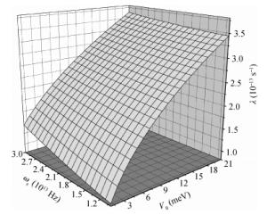
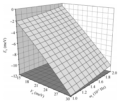
The effects of a magnetic field on the vibrational frequency, the ground state energy and the ground state binding energy of a weak-coupling polaron in asymmetrical Gaussian confinement potential quantum well (AGCPQW) are investigated by using linear combination operator and unitary transformation methods.Our calculated results show that the vibrational frequency increases with increasing cyclotron frequency of the magnetic field;meanwhile, the absolute value of the ground state energy and the ground state binding energy decrease.The vibrational frequency, the absolute value of the ground state energy and the ground state binding energy are increasing functions of the barrier height of the AGCPQW.It is shown that the barrier height of the AGCPQW and the magnetic field are important factors that influence the properties of the magnetopolaron in AGCPQW.


J. Semicond.
2015, 36(10): 102005 doi: 10.1088/1674-4926/36/10/102005

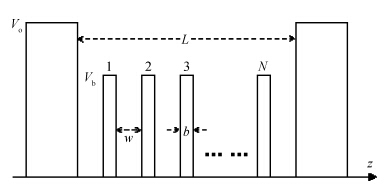
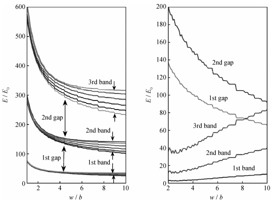
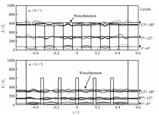
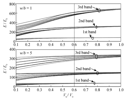
The coupling effects of quantum wells on band structure are numerically investigated by using the Matlab programming language.In a one dimensional finite quantum well with the potential barrier V0, the calculation is performed by increasing the number of inserted barriers with the same height Vb, and by, respectively, varying the thickness ratio of separated wells to inserted barriers and the height ratio of Vb to V0.Our calculations show that coupling is strongly influenced by the above parameters of the inserted barriers and wells.When these variables change, the width of the energy bands and gaps can be tuned.Our investigation shows that it is possible for quantum wells to achieve the desired width of the bands and gaps.

J. Semicond.
2015, 36(10): 102006 doi: 10.1088/1674-4926/36/10/102006

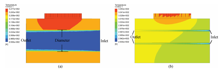
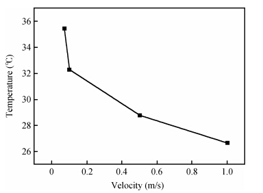
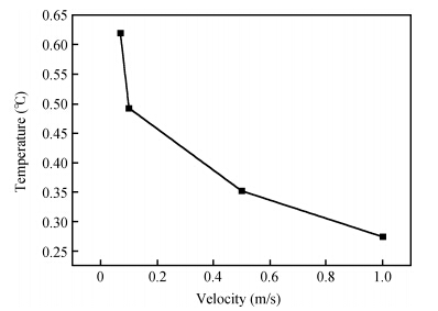
A novel high-efficiency cooling mini-channel heat-sink structure has been designed to meet the package technology demands of high power density laser diode array stacks.Thermal and water flowing characteristics have been simulated using the Ansys-Fluent software.Owing to the increased effective cooling area, this mini-channel heat-sink structure has a better cooling effect when compared with the traditional macro-channel heat-sinks.Owing to the lower flow velocity in this novel high efficient cooling structure, the chillers' water-pressure requirement is reduced.Meanwhile, the machining process of this high-efficiency cooling mini-channel heat-sink structure is simple and the cost is relatively low, it also has advantages in terms of high durability and long lifetime.This heat-sink is an ideal choice for the package of high power density laser diode array stacks.


J. Semicond.
2015, 36(10): 103001 doi: 10.1088/1674-4926/36/10/103001
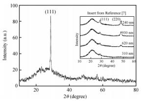
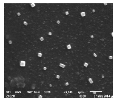
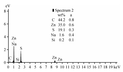
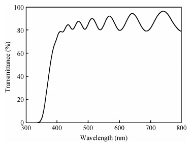
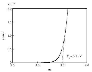
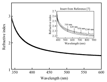
ZnS thin films were deposited on a glass substrate by thermal evaporation from millimetric crystals of ZnS.The structural, compositional and optical properties of the films are studied by X-ray diffraction, SEM microscopy, and UV-VIS spectroscopy.The obtained results show that the films are pin hole free and have a cubic zinc blend structure with (111) preferential orientation.The estimated optical band gap is 3.5 eV and the refractive index in the visible wavelength ranges from 2.5 to 1.8.The good cubic structure obtained for thin layers enabled us to conclude that the prepared ZnS films may have application as buffer layer in replacement of the harmful CdS in CIGS thin film solar cells or as an antireflection coating in silicon-based solar cells.

J. Semicond.
2015, 36(10): 103002 doi: 10.1088/1674-4926/36/10/103002
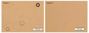
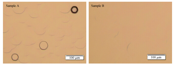
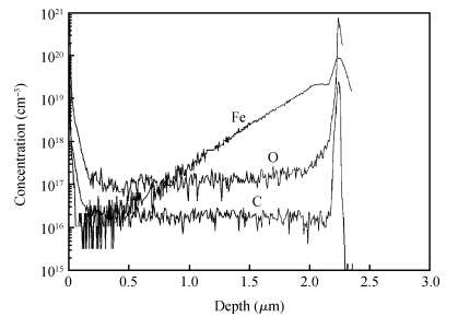
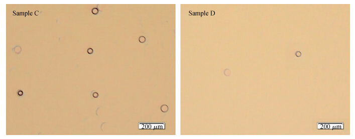
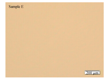
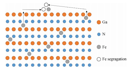
Fe doping is an effective method to obtain high resistivity GaN epitaxial material.But in some cases, Fe doping could result in serious deterioration of the GaN material surface topography, which will affect the electrical properties of two dimensional electron gas (2DEG) in HEMT device.In this paper, the influence of Fe doping on the surface topography of GaN epitaxial material is studied.The results of experiments indicate that the surface topography of Fe-doped GaN epitaxial material can be effectively improved and the resistivity could be increased after increasing the growth rate of GaN materials.The GaN material with good surface topography can be manufactured when the Fe doping concentration is 9×1019 cm-3.High resistivity GaN epitaxial material which is 1×10⁹Ω·cm is achieved.
J. Semicond.
2015, 36(10): 104001 doi: 10.1088/1674-4926/36/10/104001
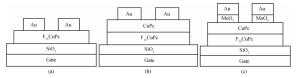
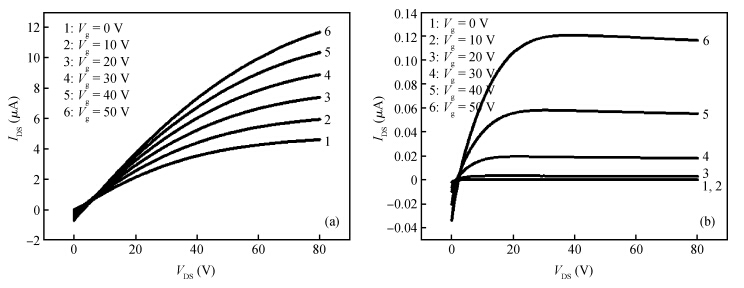
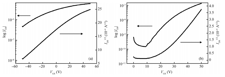
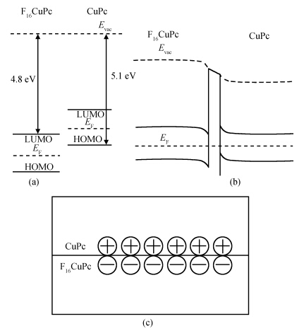
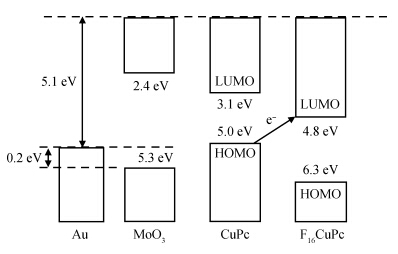
We fabricated heterojunction organic field-effect transistors (OFETs) using copper phthalocyanine (CuPc) and hexadecafluorophtholocyaninatocopper (F16CuPc) as hole transport layer and electron transport layer, respectively.Compared with F16CuPc based OFETs, the electron field-effect mobility in the heterojunction OFETs increased from 3.1×10⁻³ to 8.7×10⁻³ cm2/(V·s), but the p-type behavior was not observed.To enhanced the hole injection, we modified the source-drain electrodes using the MoO3 buffer layer, and the hole injection can be effectively improved.Eventually, the ambipolar transport characteristics of the CuPc/F16CuPc based OFETs with a MoO3 buffer layer were achieved, and the field-effect mobilities of electron and hole were 2.5×10⁻³ and 3.1×10⁻³ cm2/(V·s), respectively.


J. Semicond.
2015, 36(10): 104002 doi: 10.1088/1674-4926/36/10/104002

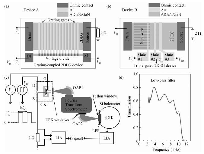
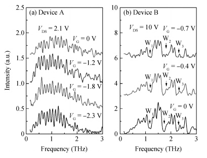
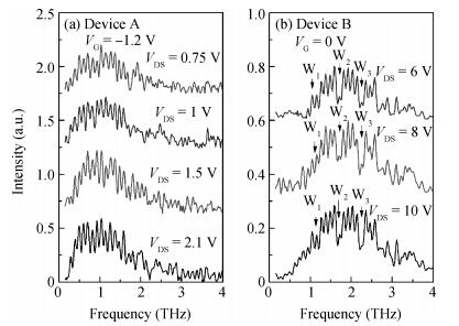
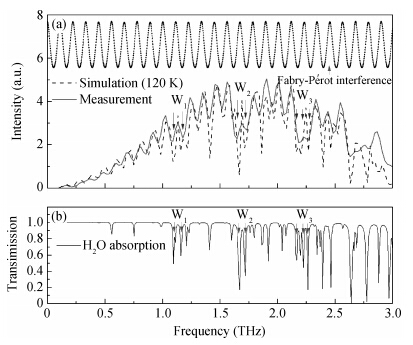
The broadband terahertz emission from drifting two-dimensional electron gas (2DEG) in an Al-GaN/GaN heterostructure at 6 K is reported.The devices are designed as THz plasmon emitters according to the Smith-Purcell effect and the 'shallow water' plasma instability mechanism in 2DEG.Plasmon excitation is excluded since no signature of electron-density dependent plasmon mode is observed.Instead, the observed THz emission is found to come from the heated lattice and/or the hot electrons.Simulated emission spectra of hot electrons taking into account the THz absorption in air and Fabry-Pérot interference agree well with the experiment.It is confirmed that a blackbody-like THz emission will inevitably be encountered in similar devices driven by a strong in-plane electric field.A conclusion is drawn that a more elaborate device design is required to achieve efficient plasmon excitation and THz emission.
J. Semicond.
2015, 36(10): 104003 doi: 10.1088/1674-4926/36/10/104003
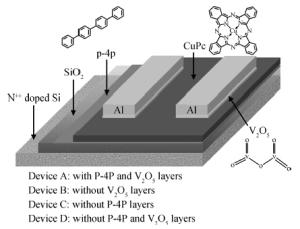
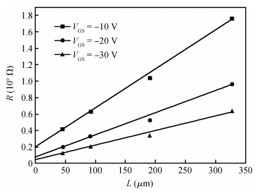
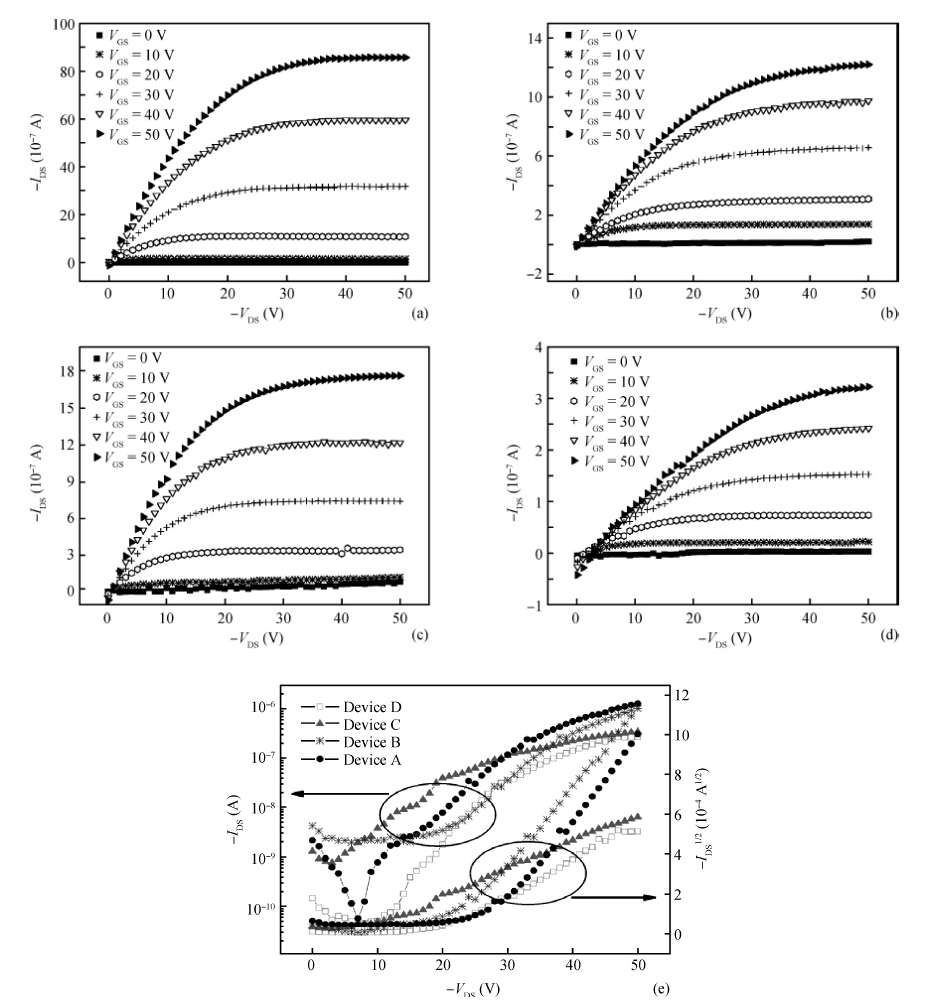
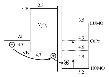
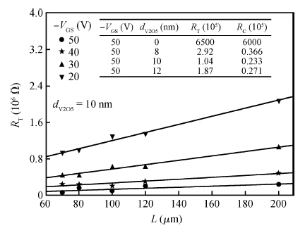
We report an effective method to improve the performance of p-type copper phthalocyanine (CuPc) based organic field-effect transistors (OFETs) by employing a thin para-quaterphenyl (p-4p) film and simultaneously applying V2O5 to the source/drain regions.The p-4p layer was inserted between the insulating layer and the active layer, and V2O5 layer was added between CuPc and Al in the source-drain (S/D) area.As a result, the fieldeffect saturation mobility and on/off current ratio of the optimized device were improved to 5×10⁻² cm2/(V·s) and 104, respectively.We believe that because p-4p could induce CuPc to form a highly oriented and continuous film, this resulted in the better injection and transport of the carriers.Moreover, by introducing the V2O5 electrode's modified layers, the height of the carrier injection barrier could be effectively tuned and the contact resistance could be reduced.


J. Semicond.
2015, 36(10): 104004 doi: 10.1088/1674-4926/36/10/104004
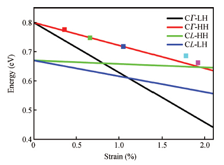
Ge has become a promising material for Si-based optoelectronic integrated circuits (OEIC) due to its pseudo-direct bandgap.In this paper we achieved tensilely strained Ge free-standing nanomembrane (NM) lightemitting diode (LED), using silicon nitride thin film with high stress.The tensile stress in the Ge layer can be controlled by adjustable process parameters.An expected redshift of electroluminescence (EL) in Ge NM LED is observed at room temperature, which has been attributed to the shrinking of its direct bandgap relative to its indirect bandgap.An EL with dramatically increased intensity was observed around 1876 nm at a tensile strain of 1.92%, which demonstrates the direct-band recombination in tensilely strained Ge NM.


J. Semicond.
2015, 36(10): 104005 doi: 10.1088/1674-4926/36/10/104005

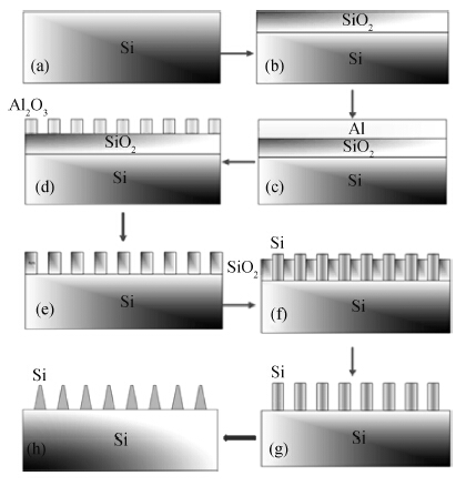
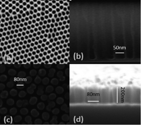
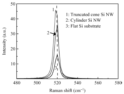
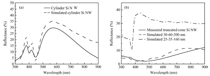
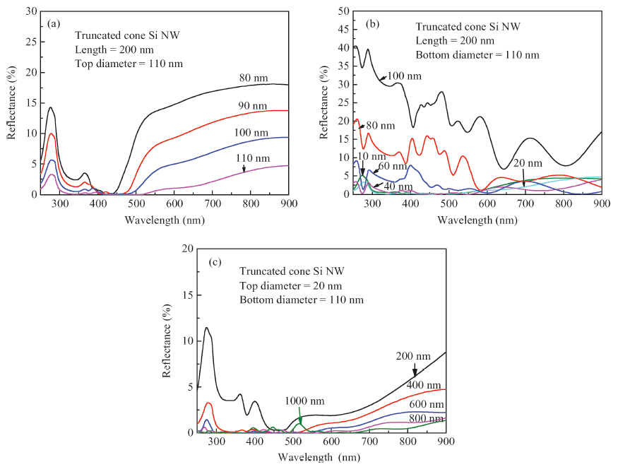
Light trapping plays an important role in improving the conversion efficiency of thin-film solar cells.The good wideband light trapping is achieved using our periodically truncated cone Si nanowire (NW) structures, and their inherent mechanism is analyzed and simulated by FDTD solution software.Ordered cylinder Si (NW) structure with initial size of 80 nm and length of 200 nm is grown by pattern transfer and selective epitaxial growth.Truncated cone Si NW array is then obtained by thermal oxidation treatment.Its mean reflection in the range of 300-900 nm is lowered to be 5% using 140 nm long truncated cone Si NW structure, compared with that of 20% using cylinder counterparts.It indicates that periodically truncated Si cone structures trap the light efficiently to enhance the light harvesting in a wide spectral range and have the potential application in highly efficient NW solar cells.


J. Semicond.
2015, 36(10): 104006 doi: 10.1088/1674-4926/36/10/104006
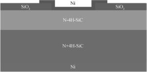
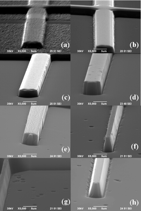
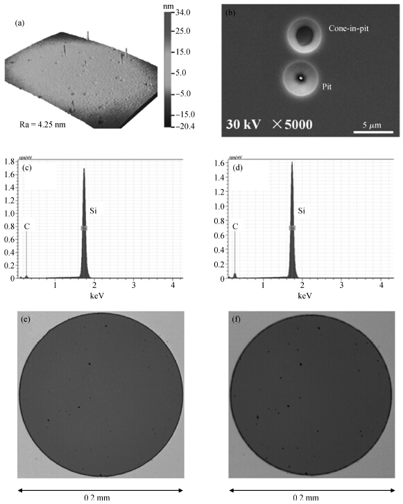
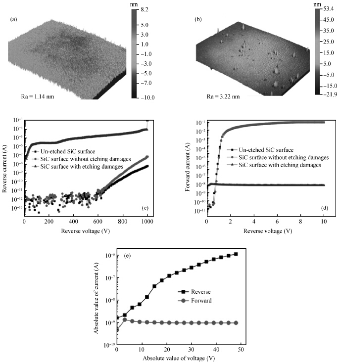
Inductively coupled plasma (ICP) etching of 4H-SiC using SF6/O2 gas mixture was studied systematically and the effect of etching was examined by metal field plate SiC Schottky diodes (SBDs). It was found that the etch rate as well as SiC surface morphology were related with ICP power, RF power, pressure, the flow of SF6 and O2.Etching damages (the cone-in-pits and pits) generated at high chuck self-bias were observed, and they were thought to be caused by SiC defects. The degradation of both the reverse and forward I-V performances of SiC SBDs was ascribed to the cone-in-pits and pits. Moreover, the absolute value of forward current is even less than the reverse counterpart in the absolute value voltage range of 0-50 V for SiC SBDs with etching damages.

J. Semicond.
2015, 36(10): 104007 doi: 10.1088/1674-4926/36/10/104007
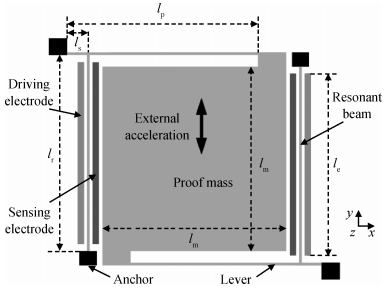
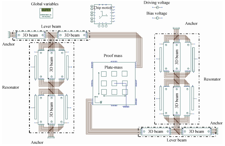
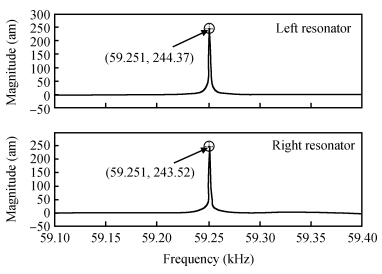
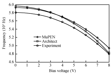
Geometric nonlinear behaviors of micro resonators have attracted extensive attention of MEMS (microelectro-mechanical systems) researchers, and MEMS transducers utilizing these behaviors have been widely researched and used due to the advantages of essentially digital output.Currently, the design of transducers with nonlinear behaviors is mainly performed by numerical method and rarely by system level design method.In this paper, the geometric nonlinear beam structure was modeled and established as a reusable library component by system level modeling and simulation method MuPEN (multi port element network).A resonant accelerometer was constructed and simulated using this model together with MuPEN reusable library.The AC (alternating current) analysis results of MuPEN model agreed well with the results of architect model and the experiment results shown in the existing reference.Therefore, we are convinced that the beam component based on MuPEN method is valid, and MEMS system level design method and related libraries can effectively model and simulate transducers with geometric nonlinear behaviors if appropriate system level components are available.


J. Semicond.
2015, 36(10): 105001 doi: 10.1088/1674-4926/36/10/105001
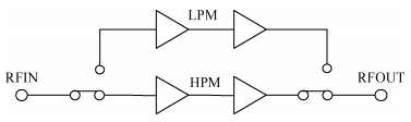
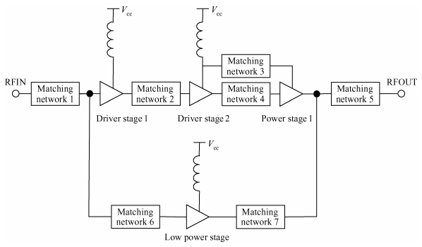
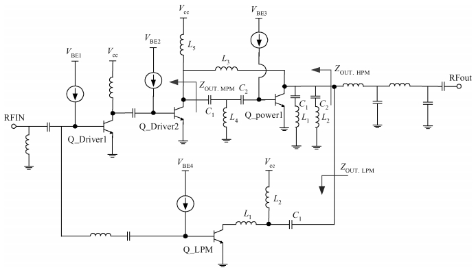
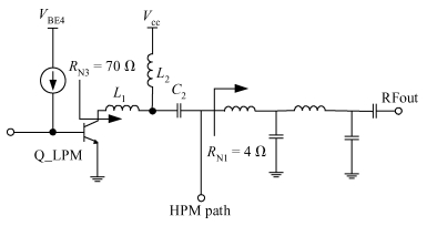
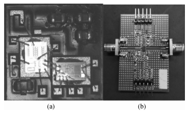
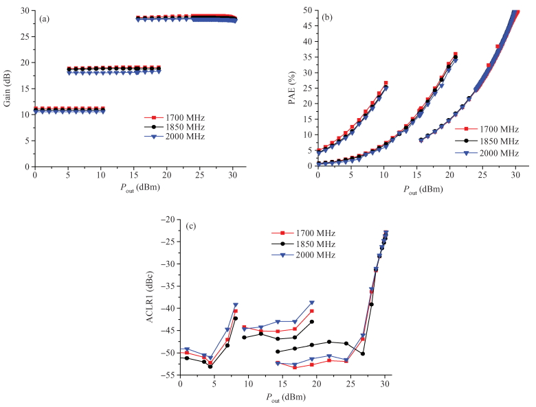
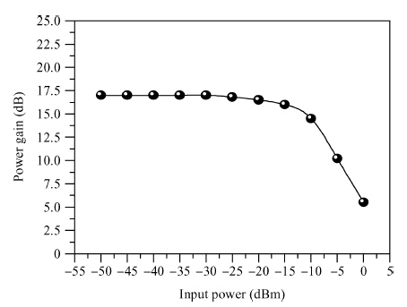
Increasingly, mobile communications standards require high power efficiency and low currents in the low power mode.This paper proposes a fully-integrated multi-mode and multi-band power amplifier module (PAM) to meet these requirements.A dual-path PAM is designed for high-power mode (HPM), medium-power mode (MPM), and low-power mode (LPM) operations without any series switches for different mode selection.Good performance and significant current saving can be achieved by using an optimized load impedance design for each power mode.The PAM is tapeout with the InGaP/GaAs heterojunction bipolar transistor (HBT) process and the 0.18-μm complementary metal-oxide semiconductor (CMOS) process.The test results show that the PAM achieves a very low quiescent current of 3 mA in LPM.Meanwhile, across the 1.7-2.0 GHz frequency, the PAM performs well.In HPM, the output power is 28 dBm with at least 39.4% PAE and-40 dBc adjacent channel leakage ratio 1 (ACLR1).In MPM, the output power is 17 dBm, with at least 21.3% PAE and-43 dBc ACLR1.In LPM, the output power is 8 dBm, with at least 18.2% PAE and -40 dBc ACLR1.


J. Semicond.
2015, 36(10): 105002 doi: 10.1088/1674-4926/36/10/105002
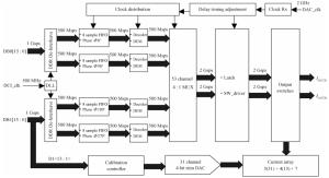
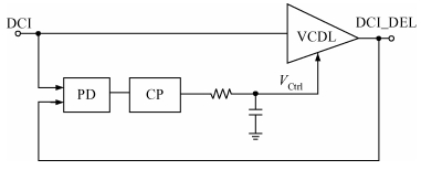
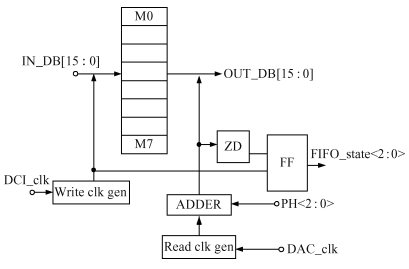
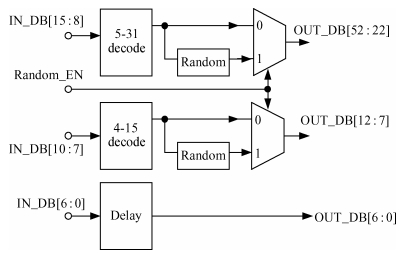
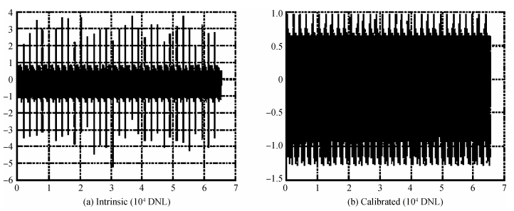
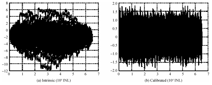
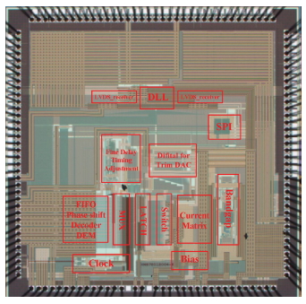
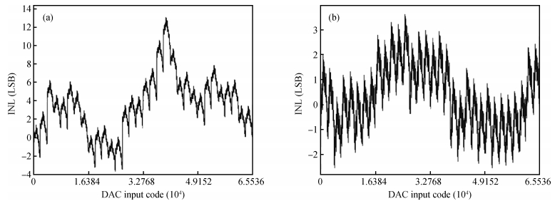
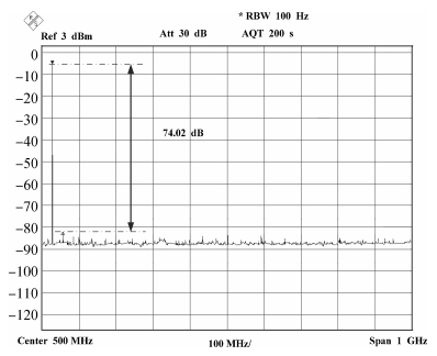
This paper presents a 16-bit 2 GSPS digital-to-analog converter (DAC) in 0.18μm CMOS technology.This DAC is implemented using time division multiplex access system architecture in the digital domain.The input data is received with a two-channel LVDS interface.The DLL technology is introduced to meet the timing requirements between phases of the LVDS data and the data sampling clock.A FIFO is designed to absorb the phase difference between the data clock and DAC system clock.A delay controller is integrated to adjust the phase relationship between the high speed digital clock and analog clock, obtaining a sampling rate of 2 GSPS.The current source mismatch at higher bits is calibrated in the digital domain.Test results show that the DAC achieves 74.02 dBC SFDR at analog output of 36 MHz, and DNL less than ±2.1 LSB INL less than ±4.3 LSB after the chip is calibrated.


J. Semicond.
2015, 36(10): 105003 doi: 10.1088/1674-4926/36/10/105003
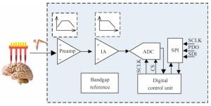
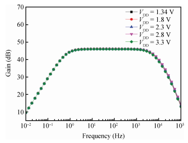
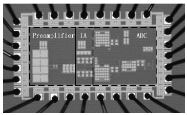
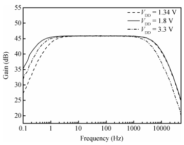
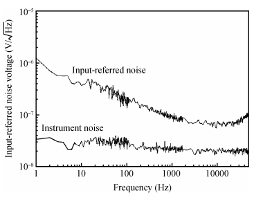
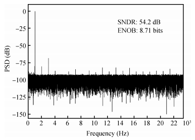
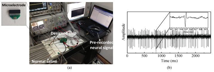
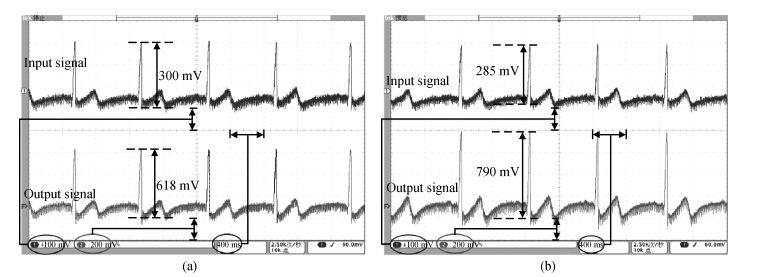
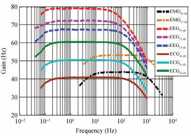
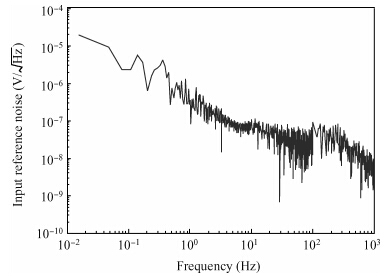
A design for a CMOS frontend integrated circuit (chip) for neural signal acquisition working at wide voltage supply range is presented in this paper.The chip consists of a preamplifier, a serial instrumental amplifier (IA) and a cyclic analog-to-digital converter (CADC).The capacitive-coupled and capacitive-feedback topology combined with MOS-bipolar pseudo-resistor element is adopted in the preamplifier to create a-3 dB upper cut-off frequency less than 1 Hz without using a ponderous discrete device.A dual-amplifier instrumental amplifier is used to provide a low output impedance interface for ADC as well as to boost the gain.The preamplifier and the serial instrumental amplifier together provide a midband gain of 45.8 dB and have an input-referred noise of 6.7 μVrms integrated from 1 Hz to 5 kHz.The ADC digitizes the amplified signal at 12-bits precision with a highest sampling rate of 130 kS/s.The measured effective number of bits (ENOB) of the ADC is 8.7 bits.The entire circuit draws 165 to 216 μ<A current from the supply voltage varied from 1.34 to 3.3 V.The prototype chip is fabricated in the 0.18-m CMOS process and occupies an area of 1.23 mm2 (including pads).In-vitro recording was successfully carried out by the proposed frontend chip.


J. Semicond.
2015, 36(10): 105004 doi: 10.1088/1674-4926/36/10/105004
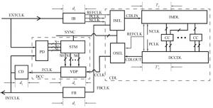
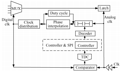
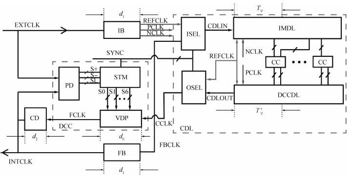
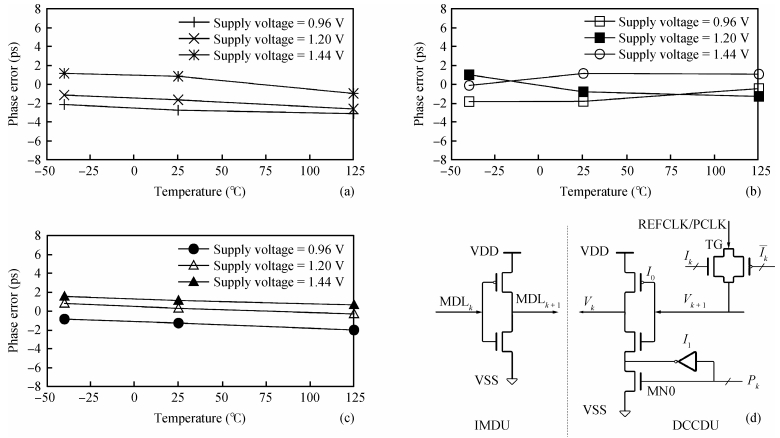
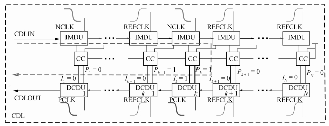
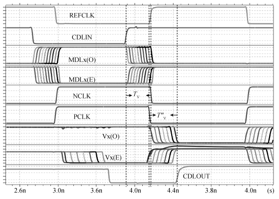
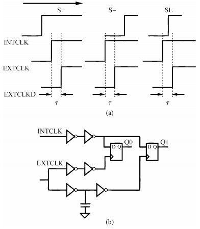
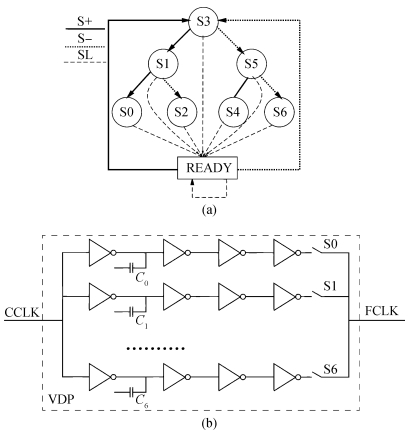
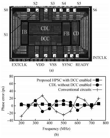
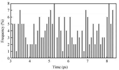
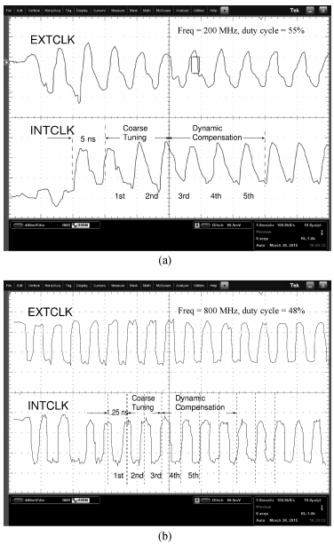
In this paper, a novel structure of a high-precision synchronization circuit, HPSC, using interleaved delay units and a dynamic compensation circuit is proposed.HPSCs are designed for synchronization of clock distribution networks in large-scale integrated circuits, where high-quality clocks are required.The application of a hybrid structure of a coarse delay line and dynamic compensation circuit performs roughly the alignment of the clock signal in two clock cycles, and finishes the fine tuning in the next three clock cycles with the phase error suppressed under 3.8 ps.The proposed circuit is implemented and fabricated using a SMIC 0.13 μm 1P6M process with a supply voltage at 1.2 V.The allowed operation frequency ranges from 200 to 800 MHz, and the duty cycle ranges between [20%,80%].The active area of the core circuits is 245×134 μm2, and the power consumption is 1.64 mW at 500 MHz.

J. Semicond.
2015, 36(10): 105005 doi: 10.1088/1674-4926/36/10/105005
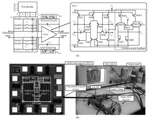
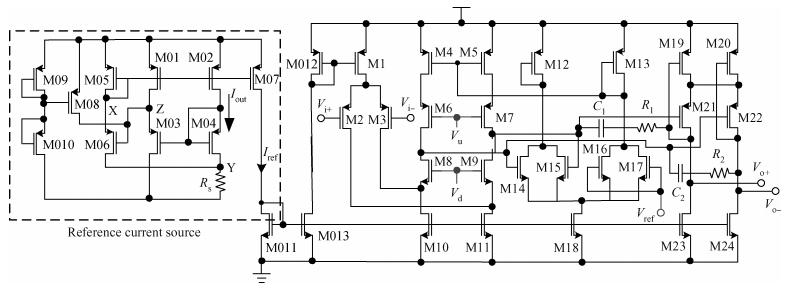
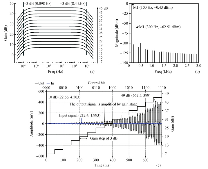
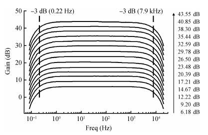
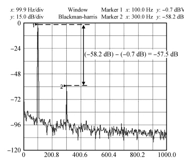
We present both a theoretical and experimental demonstration of a fully differential variable gain amplifier (VGA) with small total harmonic distortion (THD) for an electrocardiogram (ECG) acquisition system.Capacitive feedback technology is adopted to reduce the nonlinearity of VGA.The fully differential VGA has been fabricated in SMIC 0.18-μm CMOS process, and it only occupies 0.11 mm2.The measurements are in good agreement with simulation results.Experimental results show that the gain of VGA changes from 6.17 to 43.75 dB with a gain step of 3 dB.The high-pass corner frequency and low-pass corner frequency are around 0.22 Hz and 7.9 kHz, respectively.For each gain configuration, a maximal THD of 0.13% is obtained.The fully differential VGA has a low THD and its key performance parameters are well satisfied with the demands of ECG acquisition system application in the UWB wireless body area network.

J. Semicond.
2015, 36(10): 105006 doi: 10.1088/1674-4926/36/10/105006

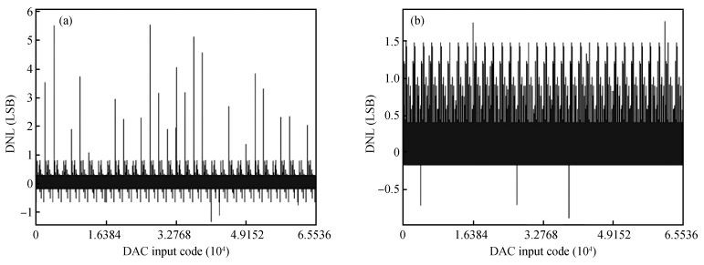
This paper presents a single-ended 8-channel 10-bit 200 kS/s 607 μW synchronous successive approximation register (SAR) analog-to-digital converter (ADC) using HLMC 55 nm low leakage (LL) CMOS technology with a 3.3 V/1.2 V supply voltage.In conventional binary-encoded SAR ADCs the total capacitance grows exponentially with resolution.In this paper a CR hybrid DAC is adopted to reduce both capacitance and core area.The capacitor array resolves 4 bits and the other 6 bits are resolved by the resistor array.The 10-bit data is acquired by thermometer encoding to reduce the probability of DNL errors which are typically present in binary weighted architectures.This paper uses an auto-zeroing offset cancellation technique that can reduce the offset to 0.286 mV.The prototype chip realized the 10-bit SAR ADC fabricated in HLMC 55 nm CMOS technology with a core area of 167×87 μm2.It shows a sampling rate of 200 kS/s and low power dissipation of 607 μW operates at a 3.3 V analog supply voltage and a 1.2 V digital supply voltage.At the input frequency of 10 kHz the signal-to-noise-anddistortion ratio (SNDR) is 60.1 dB and the spurious-free dynamic range (SFDR) is 68.1 dB.The measured DNL is +0.37/-0.06 LSB and INL is +0.58/-0.22 LSB.


J. Semicond.
2015, 36(10): 105007 doi: 10.1088/1674-4926/36/10/105007
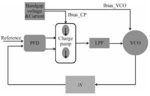
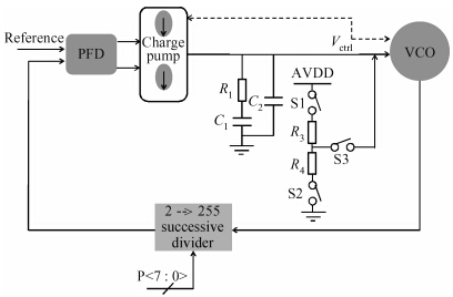
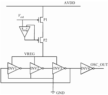
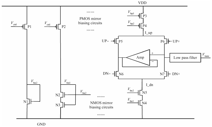
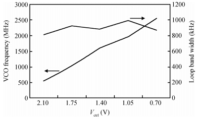
A new low power, low phase jitter, compact realization, and self-biased PLL, which is fabricated on SMIC 40 nm CMOS technology is introduced.The proposed self-biased PLL eliminates extra band gap biasing circuits, and internally generates all the biasing voltages and currents.Meanwhile, all of the PLL dynamic loop parameters, such as loop bandwidth, natural frequency, damping factors are kept constant adaptively.By optimizing the circuit structures, the perfect unity of chip estate, power dissipation, phase jitter, and loop stability is achieved.The PLL consumes 4.2 mW of power under 1.1 V/2.5 V voltage supply at 2.4 GHz VCO frequency, while occupying a die area of less than 0.02 mm2 (180×110 μm2), and the typical period jitter (RMS) is around 2.8 ps.


J. Semicond.
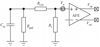
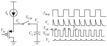
2015, 36(10): 105008 doi: 10.1088/1674-4926/36/10/105008

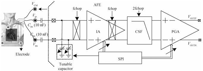
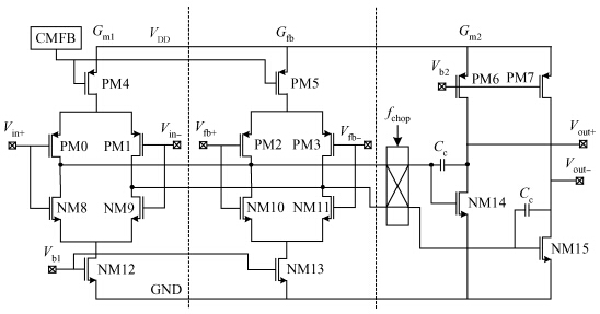
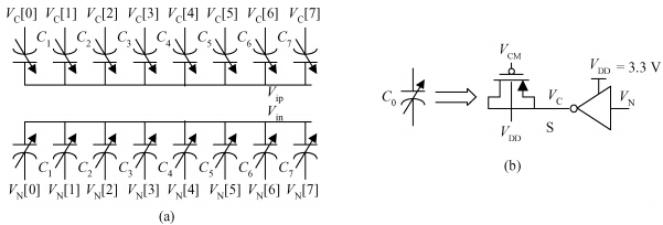
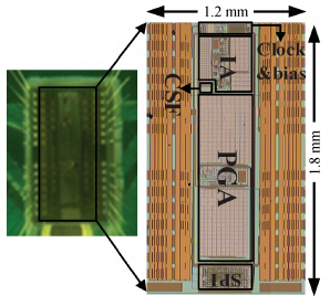
The presented analog front end (AFE) used to process human bio-signals consists of chopping instrument amplifier (IA), chopping spikes filter and programmable gain and bandwidth amplifier.The capacitorcoupling input of AFE can reject the DC electrode offset.The power consumption of current-feedback based IA is reduced by adopting capacitor divider in the input and feedback network.Besides, IA's input thermal noise is decreased by utilizing complementary CMOS input pairs which can offer higher transconductance.Fabricated in Global Foundry 0.35 μm CMOS technology, the chip consumes 3.96 μA from 3.3 V supply.The measured input noise is 0.85 μVrms (0.5-100 Hz) and the achieved noise efficient factor is 6.48.


J. Semicond.
2015, 36(10): 105009 doi: 10.1088/1674-4926/36/10/105009

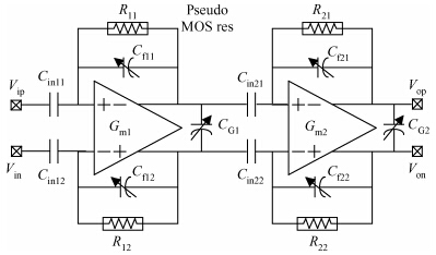
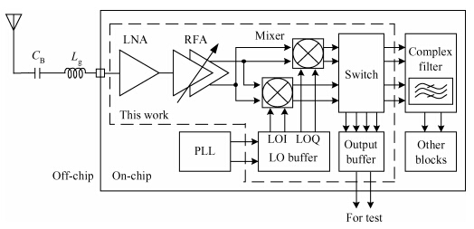
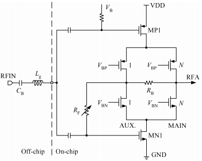
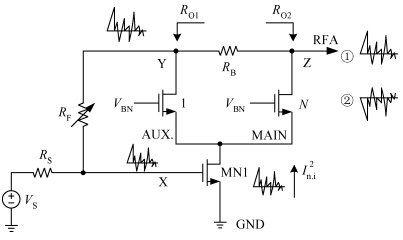
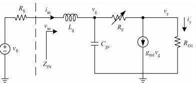
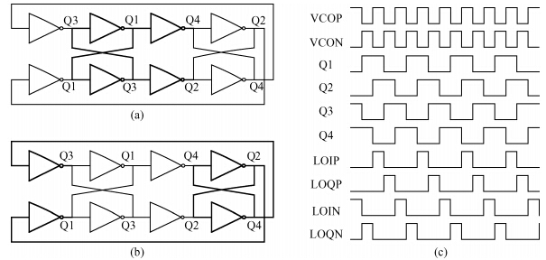
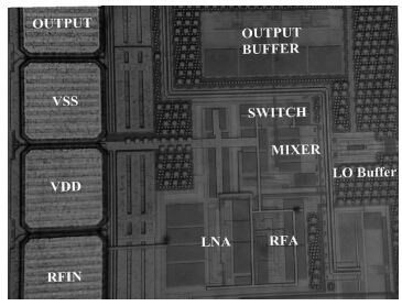
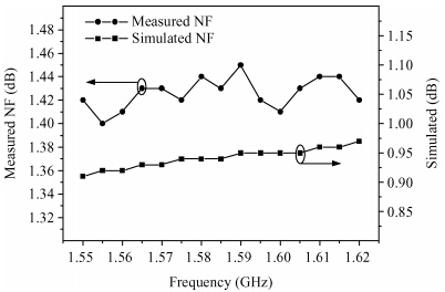
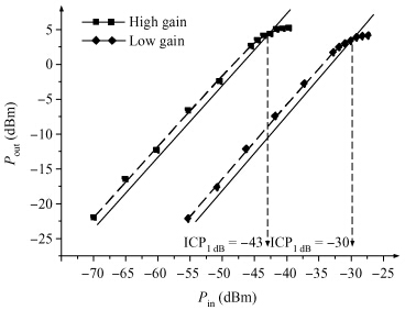
An inductorless multi-mode RF front end for a global navigation satellite system (GNSS) receiver is presented.Unlike the traditional topology of a low noise amplifier (LNA), the inductorless current-mode noisecanceling LNA is applied in this design.The high-impedance-input radio frequency amplifier (RFA) further amplifies the GNSS signals and changes the single-end signal path into fully differential.The passive mixer downconverts the signals to the intermediate frequency (IF) band and conveys the signals to the analogue blocks.The local oscillator (LO) buffer divides the output frequency of the voltage controlled oscillator (VCO) and generates 25%-duty-cycle quadrature square waves to drive the mixer.Our measurement results display that the implemented RF front end achieves good overall performance while consuming only 6.7 mA from 1.2 V supply.The input return loss is better than-26 dB and the ultra low noise figure of 1.43 dB leads to high sensitivity of the GNSS receiver.The input 1 dB compression point is-43 dBm at the high gain of 48 dB.The designed circuit is fabricated in 55 nm CMOS technology and the die area, which is much smaller than traditional circuit, is around 220×280 μm2.


J. Semicond.
2015, 36(10): 105010 doi: 10.1088/1674-4926/36/10/105010
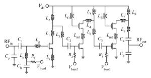
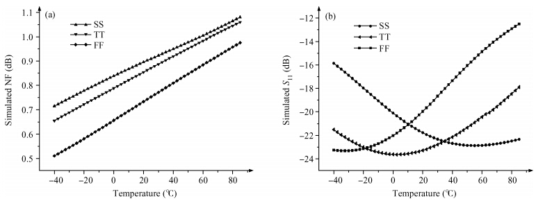
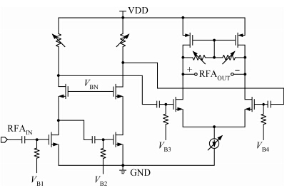
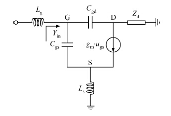
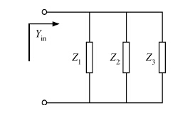
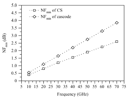
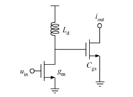
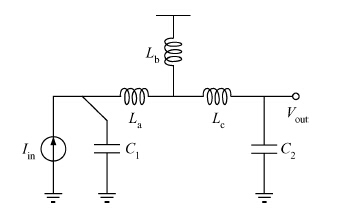
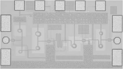
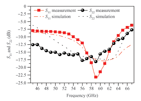
A broadband 47-67 GHz low noise amplifier (LNA) with 17.3 dB gain in 65-nm CMOS technology is proposed.The features of millimeter wave circuits are illustrated first and design methodologies are discussed.The wideband input matching of the LNA was achieved by source inductive degeneration, which is narrowband in the low-GHz range but wideband at millimeter-wave frequencies due to the existence of gate-drain capacitance, Cgd.In order to minimize the noise figure (NF), the LNA used a common-source (CS) structure rather than cascode in the first stage, and the noise matching principle is explored.The last two stages of the LNA used a cascode structure to increase the power gain.Analysis of the gain boost effect of the gate inductor at the common-gate (CG) transistor is also performed.T-shape matching networks between stages are intended to enlarge the bandwidth.All on-chip inductors and transmission lines are modeled and simulated with a 3-dimensional electromagnetic (EM) simulation tool to guarantee the success of the design.Measurement results show that the LNA achieves a maximum gain of 17.3 dB at 60 GHz, while the 3-dB bandwidth is 20 GHz (47-67 GHz), including the interested band of 59-64 GHz, and the minimum noise figure is 4.9 dB at 62 GHz.The LNA absorbs a current of 19 mA from a 1.2 V supply and the chip occupies an area of 900×550 μm2 including pads.


J. Semicond.
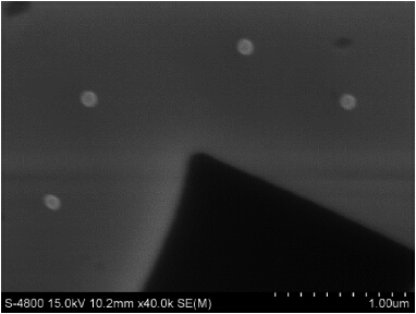
2015, 36(10): 106001 doi: 10.1088/1674-4926/36/10/106001
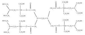
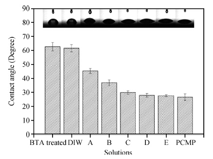
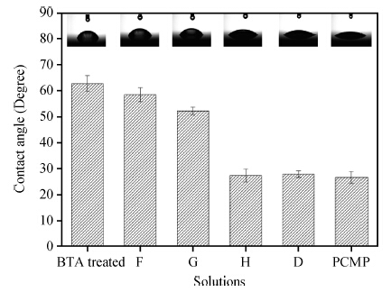
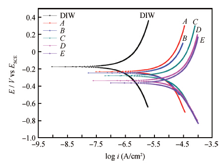
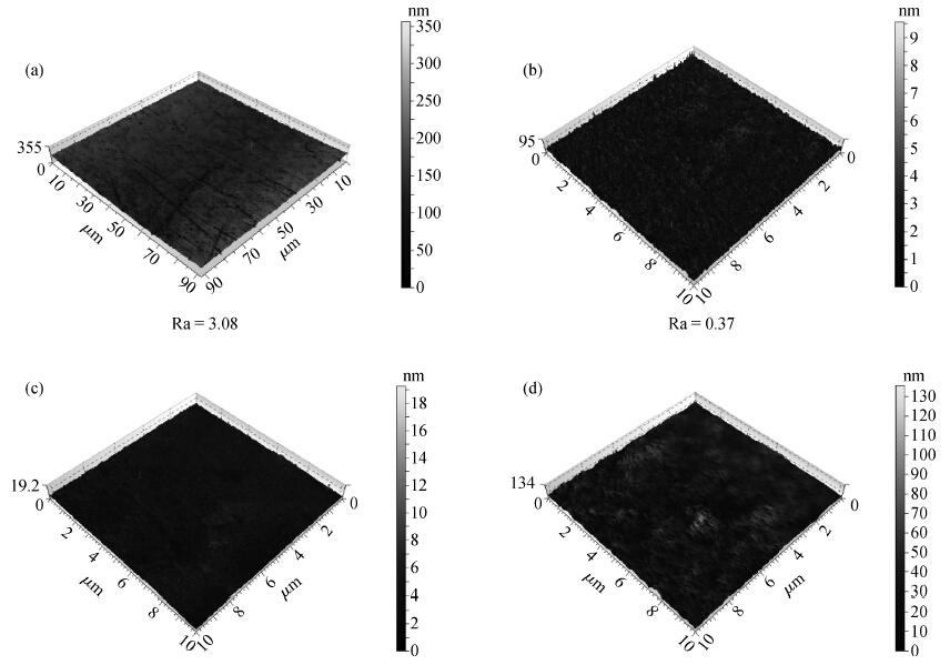
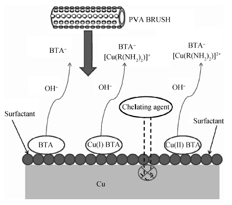
After the chemical mechanical planarization (CMP) process, the copper surface is contaminated by a mass of particles (e.g.silica) and organic residues (e.g.benzotriazole), which could do great harm to the integrated circuit, so post-CMP cleaning is essential.In particular, benzotriazole (BTA) forms a layer of Cu-BTA film with copper on the surface, which leads to a hydrophobic surface of copper.So an effective cleaning solution is needed to remove BTA from the copper surface.In this work, a new compound cleaning solution is designed to solve two major problems caused by BTA:one is removing BTA and the other is copper surface corrosion that is caused by the cleaning solution.The cleaning solution is formed of alkaline chelating agent (FA/O II type), which is used to remove BTA, and a surfactant (FA/O I type), which is used as a corrosion inhibitor.BTA removal is characterized by contact angle measurements and electrochemical techniques.The inhibiting corrosion ability of the surfactant is also characterized by electrochemical techniques.The proposed compound cleaning solution shows advantages in removing BTA without corroding the copper surface.

J. Semicond.
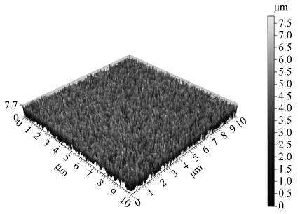
2015, 36(10): 106002 doi: 10.1088/1674-4926/36/10/106002

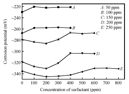
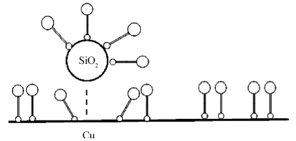
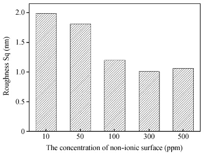
A novel cleaning solution, named FA/O alkaline cleaner, was proposed and demonstrated in the removal of colloidal silica abrasives.In order to remove both the chemical and physical absorbed colloidal silica abrasives, an FA/OII chelating agent and non-ionic surfactant were added into the cleaner.By varying the concentration of chelating agent and non-ionic surfactant, a series of experiments were performed to determine the best cleaning results.This paper discusses the mechanism of the removal of colloidal silica abrasives with a FA/O alkaline cleaner.Based on the experiment results, it is concluded that both the FA/OII chelating and non-ionic surfactant could benefit the removal of colloidal silica abrasives.When the concentration of FA/OII chelating agent and FA/O non-ionic surfactant reached the optima value, it was demonstrated that silica abrasives could be removed efficiently by this novel cleaning solution.


J. Semicond.
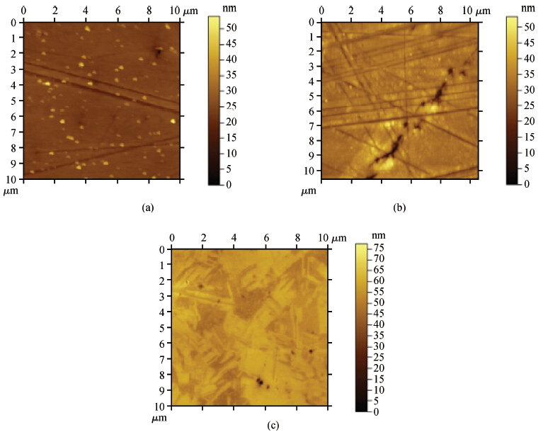
2015, 36(10): 106003 doi: 10.1088/1674-4926/36/10/106003

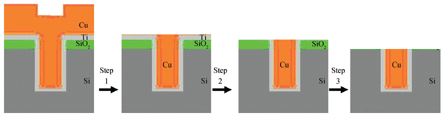
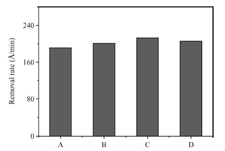
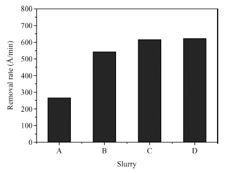
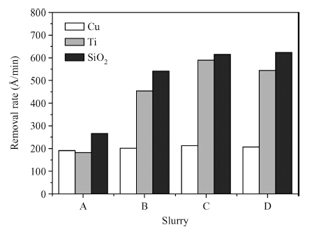
The effect of a novel alkaline TSV (through-silicon-via) slurry with guanidine hydrochloride (GH) on CMP (chemical mechanical polishing) was investigated.The novel alkaline TSV slurry was free of any inhibitors.During the polishing process, the guanidine hydrochloride serves as an effective surface-complexing agent for TSV CMP applications, the removal rate of barrier (Ti) can be chemically controlled through tuned selectivity with respect to the removal rate of copper and dielectric, which is helpful to modifying the dishing and gaining an excellent topography performance in TSV manufacturing.In this paper, we mainly studied the working mechanism of the components of slurry and the skillful application guanidine hydrochloride in the TSV slurry.