Issue Browser
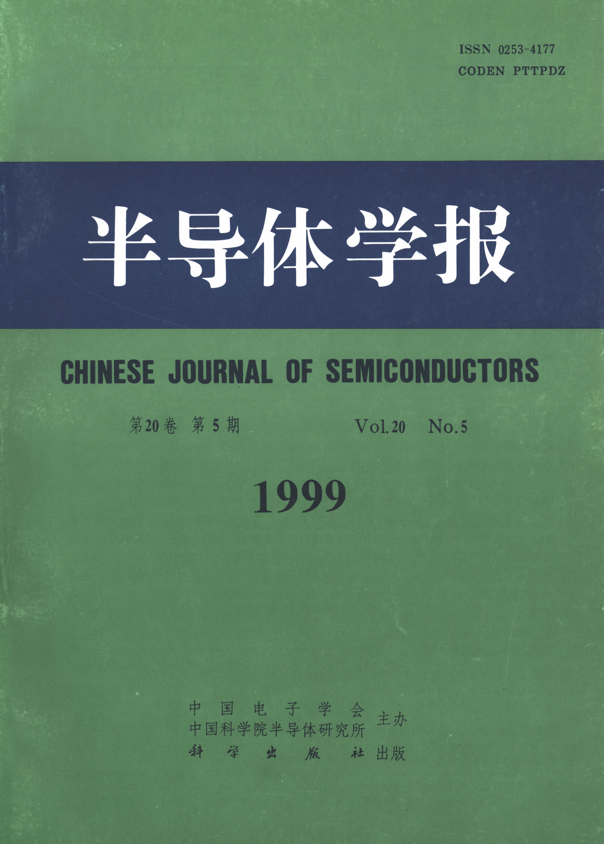
Volume 20, Issue 5, May 1999
CONTENTS
图形衬底上应变SiGe/Si超晶格的结构及光致发光研究
司俊杰, 杨沁清, 高俊华, 滕达, 王启明, 郭丽伟, 周均铭
Chin. J. Semicond.  1999, 20(5): 353-357
Abstract PDF

半导体器件热特性的电学法测量与分析
冯士维, 谢雪松, 吕长志, 张小玲, 何焱, 沈光地
Chin. J. Semicond.  1999, 20(5): 358-364
Abstract PDF

二维聚乙炔中的sp~2杂化轨道对电子跳跃能量的影响
童国平
Chin. J. Semicond.  1999, 20(5): 365-370
Abstract PDF

N型GaN的持续光电导
汪连山, 刘祥林, 岳国珍, 王晓晖, 汪度, 陆大成, 王占国
Chin. J. Semicond.  1999, 20(5): 371-377
Abstract PDF

分子束外延HgCdTe薄膜位错密度的研究
于梅芳, 杨建荣, 王善力, 陈新强, 乔怡敏, 巫艳, 何力, 韩培德
Chin. J. Semicond.  1999, 20(5): 378-382
Abstract PDF

硅表面清洗对热氧化13nm SiO_2可靠性的影响
高文钰, 刘忠立, 和致经, 于芳, 梁桂荣, 李国花
Chin. J. Semicond.  1999, 20(5): 383-388
Abstract PDF

平面掺杂异质结场效应管的二维电子气浓度和材料结构尺寸之间的关系
李效白
Chin. J. Semicond.  1999, 20(5): 389-394
Abstract PDF

TiO_2薄膜的制备及结构研究
孟宪权, 王君, 何磊, 范湘军
Chin. J. Semicond.  1999, 20(5): 395-399
Abstract PDF

基于协同工作方式的一种蚁群布线系统
庄昌文, 范明钰, 李春辉, 虞厥邦
Chin. J. Semicond.  1999, 20(5): 400-406
Abstract PDF

AlxGa1-xN and GaN/AlxGa1-xN Quantum Wells Grown by Gas Source Molecular Beam Epitaxy
Xiaoliang Wang(王晓亮), Dianzhao Sun(孙殿照), Jianping Zhang(张剑平), Meiying Kong(孔梅影), Yiping Zeng(曾一平), Jinmin Li(李晋闽), Lanying Lin(林兰英)
Chin. J. Semicond.  1999, 20(5): 407-411
Abstract PDF

A lxGa1- xN and GaN/A lxGa1- xN quantum wells were successfully grown on basal plane sapphire substrates by gas source molecular beam epitaxy using ammonia as nitrogen source. Photoluminescence measurements were carried out for the samples grown. The results show that the blue shifts in optical transition energy due to quantum size effect are 57meV at room temperature and 49meV at 80K for the GaN/Al0.12Ga0.88N quantum well sample having 6 GaN wells each with width of 7nm.

A lxGa1- xN and GaN/A lxGa1- xN quantum wells were successfully grown on basal plane sapphire substrates by gas source molecular beam epitaxy using ammonia as nitrogen source. Photoluminescence measurements were carried out for the samples grown. The results show that the blue shifts in optical transition energy due to quantum size effect are 57meV at room temperature and 49meV at 80K for the GaN/Al0.12Ga0.88N quantum well sample having 6 GaN wells each with width of 7nm.

Monolithic Integration of MQW DFB Laser and EA Modulator in 1.55μm Wavelength
Xuejing Yan(颜学进), Guoyang Xu(许国阳), Hongliang Zhu(朱洪亮), Fan Zhou(周帆), Xiaojie Wang(汪孝杰), Jingyuan Zhang(张静媛), Huiliang Tian(田慧良), Chaohua Ma(马朝华), Huiyun Shu(舒惠云), Yunxia Bai(白云霞), Kekui Bi(毕可奎), Ronghan Wu(吴荣汉), Qiming Wang(王启明), Wei Wang(王圩)
Chin. J. Semicond.  1999, 20(5): 412-415
Abstract PDF

The design and fabrication of 1.55um wavelength Multiple Quantum Well (MQW) Distributed Feedback (DFB) laser integrated with electroabsorption modulator is reported. A static single longitudinal mode output power greater than 6mW in free space is obtained, with 0V bias to the 150um length modulator and an extinction ratio of up to 11dB at 4V at 100mA operation current of 300um length DFB laser. The modulator side and DFB laser side are coated with Antireflcetion (AR) and High reflection (HR) coating respectively. The threshold current of DFB laser is about 16mA and the side mode suppression ratio is always greater than 35dB when the reverse bias voltage of the modulator is varied from 0V to 4V.

The design and fabrication of 1.55um wavelength Multiple Quantum Well (MQW) Distributed Feedback (DFB) laser integrated with electroabsorption modulator is reported. A static single longitudinal mode output power greater than 6mW in free space is obtained, with 0V bias to the 150um length modulator and an extinction ratio of up to 11dB at 4V at 100mA operation current of 300um length DFB laser. The modulator side and DFB laser side are coated with Antireflcetion (AR) and High reflection (HR) coating respectively. The threshold current of DFB laser is about 16mA and the side mode suppression ratio is always greater than 35dB when the reverse bias voltage of the modulator is varied from 0V to 4V.

2.5Gb/s1.55μm InGaAsP/InP分布反馈激光器/电吸收调制器单片集成器件
罗毅, 孙长征, 文国鹏, 李同宁, 杨新民, 吴又生, 王任凡, 王彩玲, 黄涛, 金锦炎
Chin. J. Semicond.  1999, 20(5): 416-420
Abstract PDF

金属/绝缘层/硅(MIS)隧道二极管的发光机理
俞建华, 孙承休, 高中林, 魏同立, 王启明
Chin. J. Semicond.  1999, 20(5): 421-424
Abstract PDF

四元系AlGaInP为发射极异质结双极晶体管研究
程知群, 孙晓玮, 束伟民, 张兴宏, 顾伟东, 夏冠群
Chin. J. Semicond.  1999, 20(5): 425-428
Abstract PDF

混晶GaAs_(1-x)P_x∶N(x=0.4)中的N_X和N_Γ发光带的研究
俞容文, 郑健生, 颜炳章
Chin. J. Semicond.  1999, 20(5): 429-432
Abstract PDF

利用改进的固相外延技术改善CMOS/SOS器件的特性
刘忠立, 和致经, 于芳, 张永刚, 郁元桓
Chin. J. Semicond.  1999, 20(5): 433-436
Abstract PDF

含N薄栅介质的电离辐照及退火特性
张国强, 陆妩, 余学锋, 郭旗, 任迪远, 严荣良
Chin. J. Semicond.  1999, 20(5): 437-440
Abstract PDF