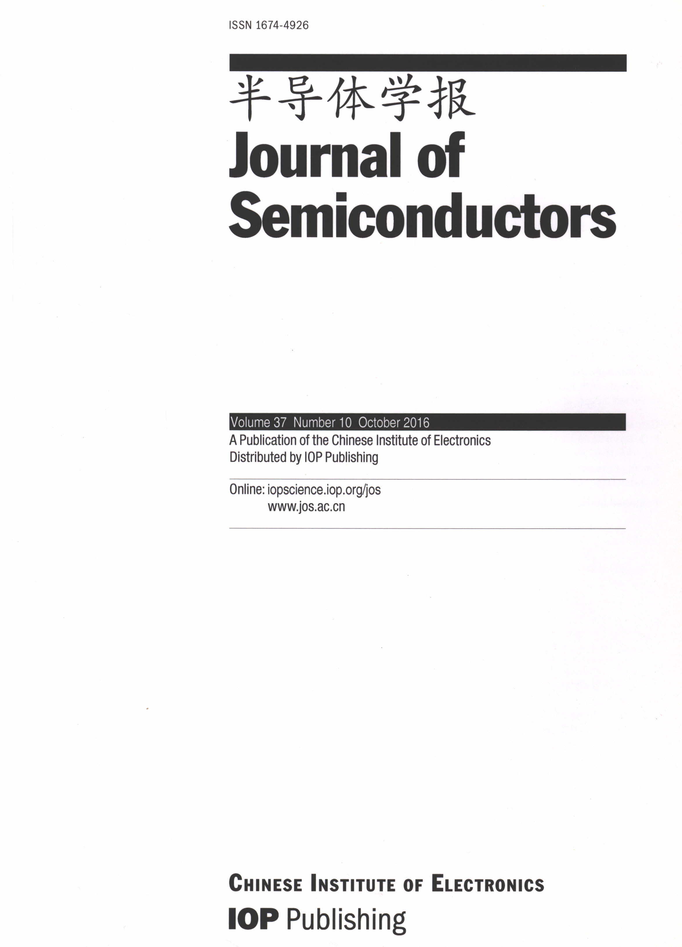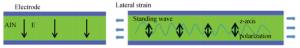
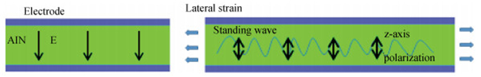
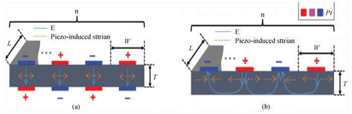
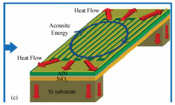
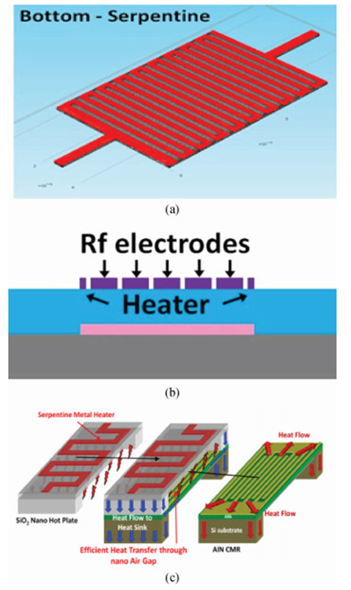
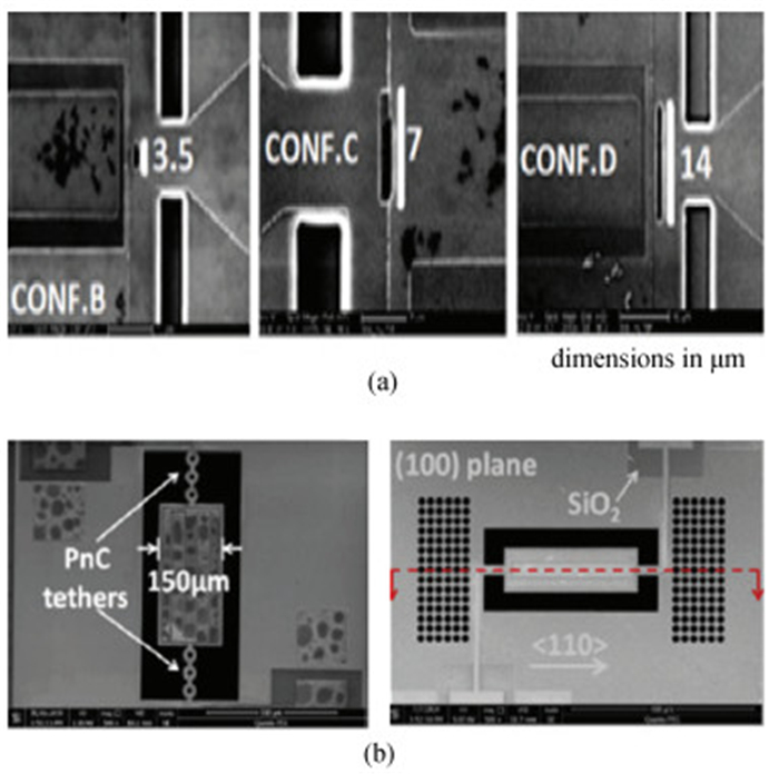
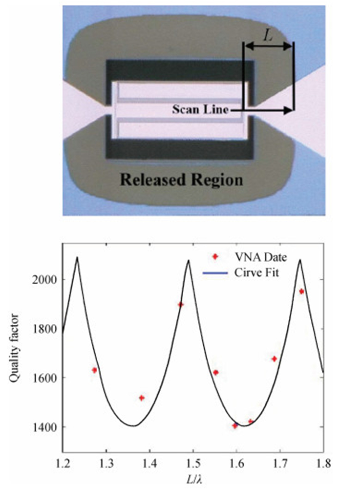
Over the past several decades, the technology of micro-electromechanical system (MEMS) has advanced. A clear need of miniaturization and integration of electronics components has had new solutions for the next generation of wireless communications. The aluminum nitride (AlN) MEMS contour-mode resonator (CMR) has emerged and become promising and competitive due to the advantages of the small size, high quality factor and frequency, low resistance, compatibility with integrated circuit (IC) technology, and the ability of integrating multi-frequency devices on a single chip. In this article, a comprehensive review of AlN MEMS CMR technology will be presented, including its basic working principle, main structures, fabrication processes, and methods of performance optimization. Among these, the deposition and etching process of the AlN film will be specially emphasized and recent advances in various performance optimization methods of the CMR will be given through specific examples which are mainly focused on temperature compensation and reducing anchor losses. This review will conclude with an assessment of the challenges and future trends of the CMR.
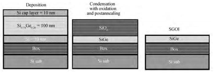
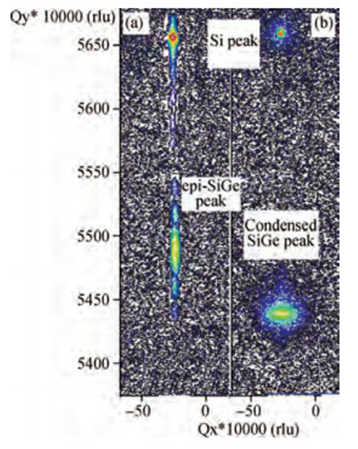
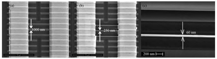
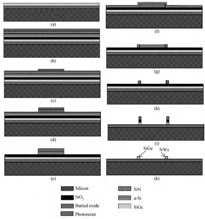
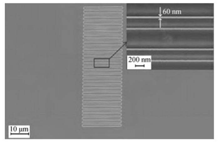
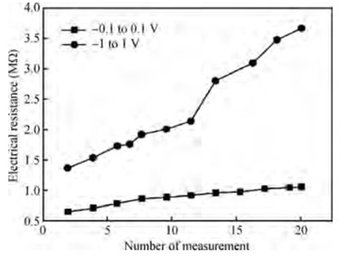
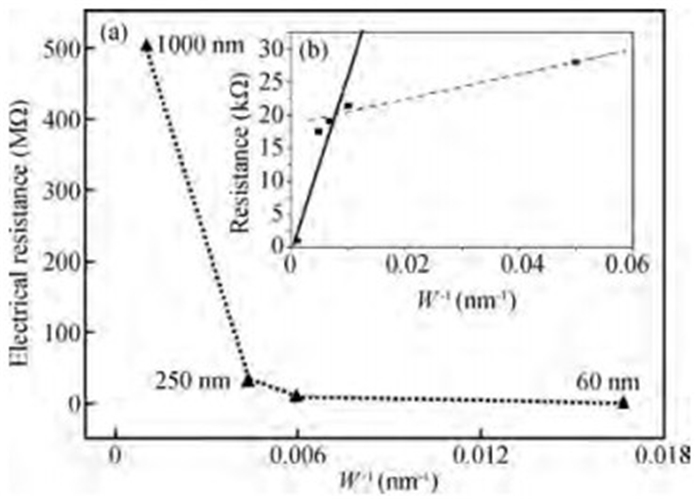
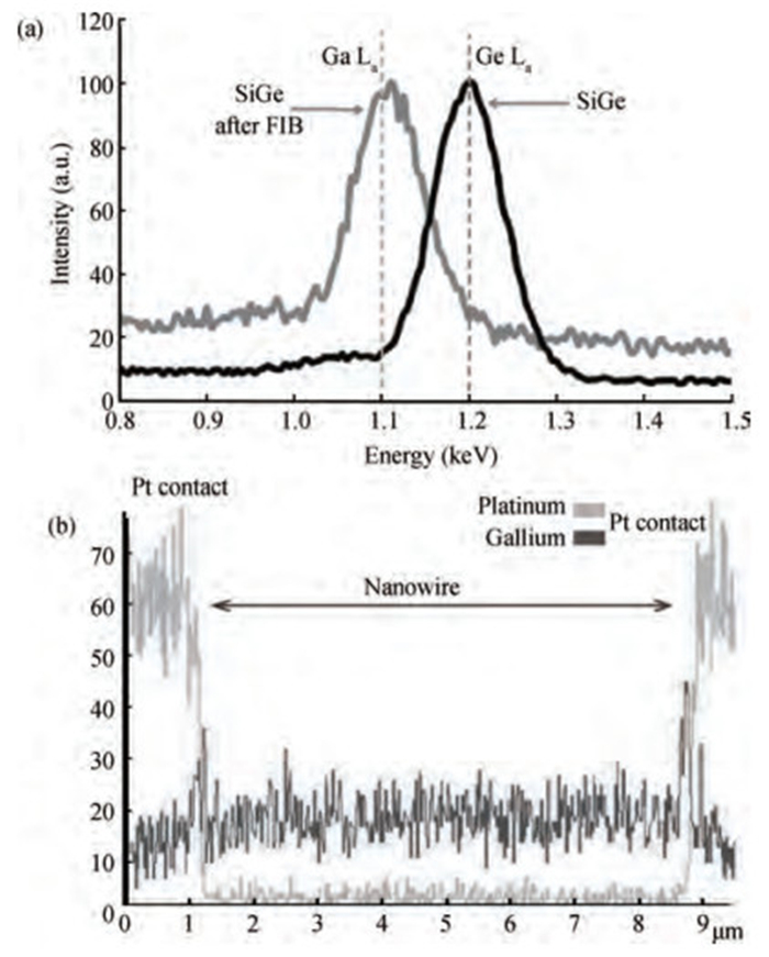
In this study, the electrical properties of SiGe nanowires in terms of process and fabrication integrity, measurement reliability, width scaling, and doping levels were investigated. Nanowires were fabricated on SiGe-on oxide (SGOI) wafers with thickness of 52 nm and Ge content of 47%. The first group of SiGe wires was initially formed by using conventional I-line lithography and then their size was longitudinally reduced by cutting with a focused ion beam (FIB) to any desired nanometer range down to 60 nm. The other nanowire group was manufactured directly to a chosen nanometer level by using sidewall transfer lithography (STL). It has been shown that the FIB fabrication process allows manipulation of the line width and doping level of nanowires using Ga atoms. The resistance of wires thinned by FIB was 10 times lower than STL wires which shows the possible dependency of electrical behavior on fabrication method.

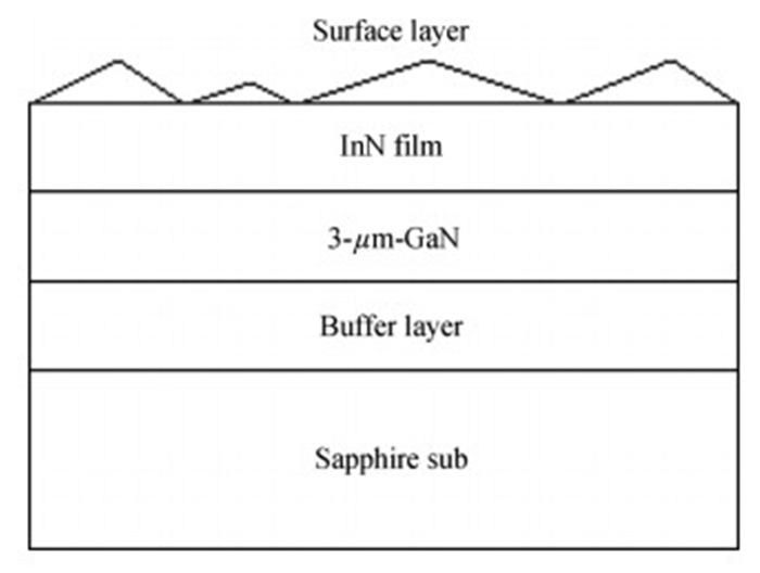
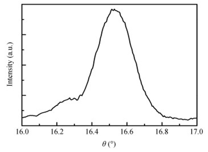
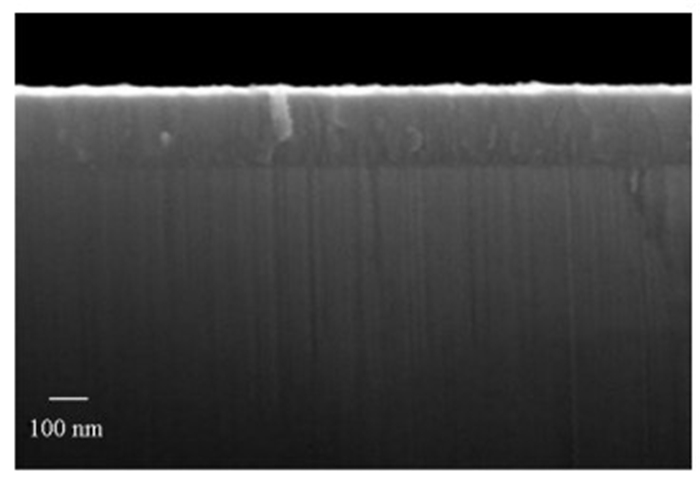
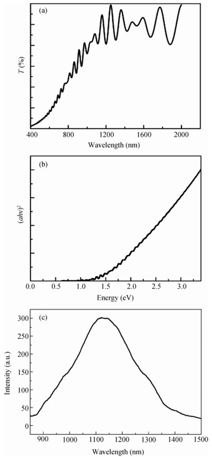
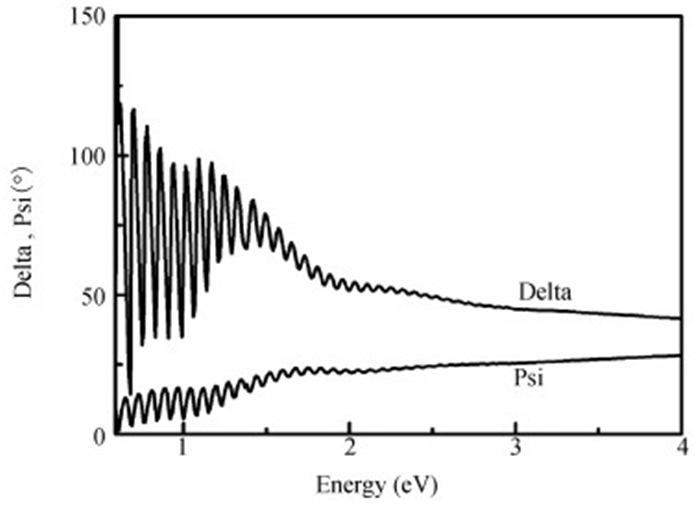
With recently developed InN epitaxy via a controlling In bilayer, spectroscopic ellipsometry (SE) measurements had been carried out on the grown InN and the measured ellipsometric spectra were fitted with the Delta Psi2 software by using a suitable model and the dispersion rule. The thickness was measured by a scanning electron microscope (SEM). Insight into the film quality of InN and the lattice constant were gained by X-ray diffraction (XRD). By fitting the SE, the thickness of the InN film is consistent with that obtained by SEM cross-sectional thickness measurement. The optical bandgap of InN was put forward to be 1.05 eV, which conforms to the experimental results measured by the absorption spectrum and cathodoluminescence (CL). The refractive index and the extinction coefficient of interest were represented for InN, which is useful to design optoelectronic devices.

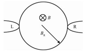
The electron transport through a Rashba ring with a magnetic flux and driven by a temperature difference is investigated. It is found that the spin interference effect induced by the Rashba spin-orbit interaction and by the magnetic flux can break the balance between the spin-up and spin-down component currents in the thermally driven charge current and thus result in a spin current. The analytical derivation and numerical calculations reveal that the magnitude, sign, peaks and spin-polarization of the generated spin current can be readily modulated by the system parameters. In particular, with some choices of the parameters, the spin polarization of the generated spin current can reach 100%, that is, a fully spin-polarized thermospin current can be produced. These results may help the use of the spin-dependent Seebeck effect to generate and manipulate a spin current.

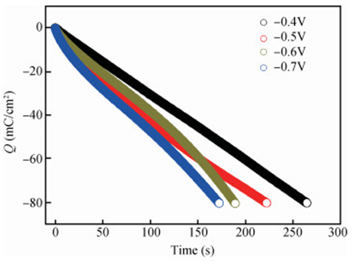
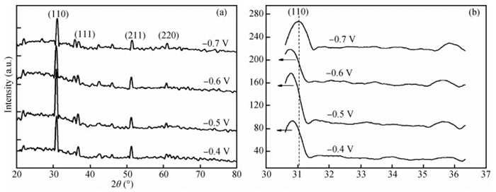
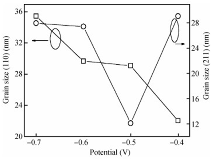
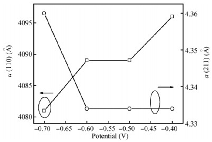
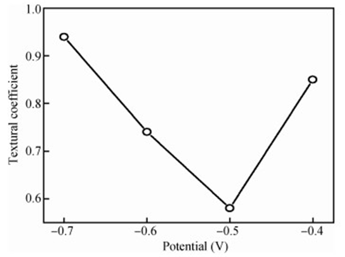
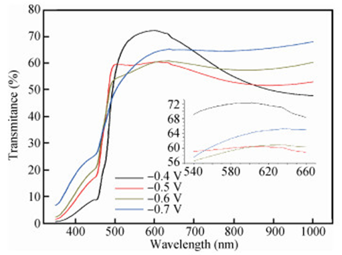
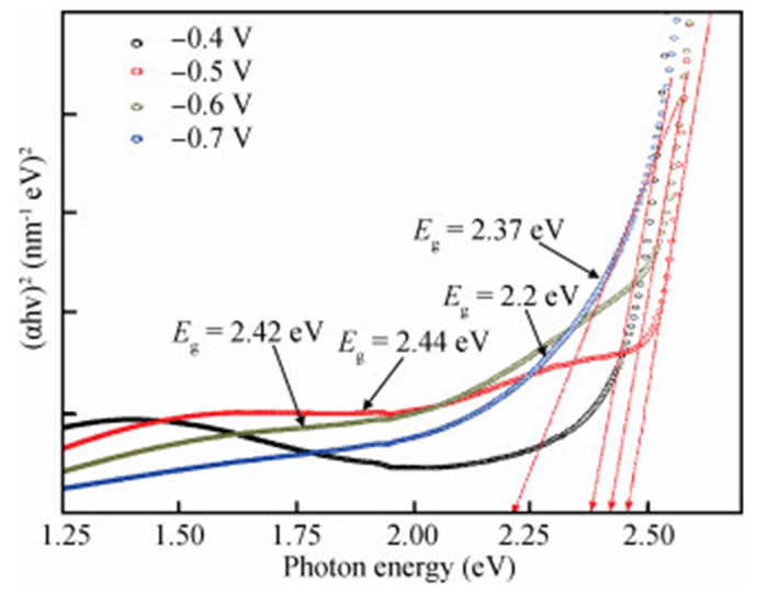
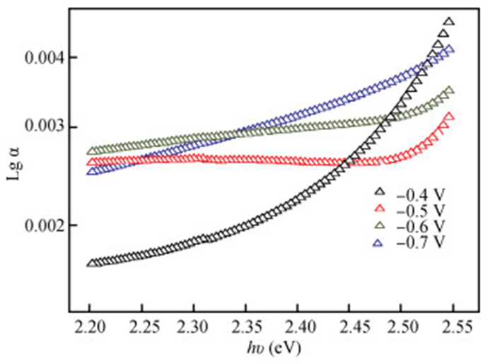
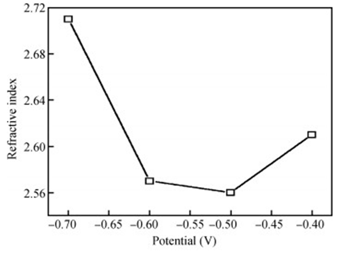
The thin films of Cu2O are deposited by electrodeposition technique onto indium tin oxide (ITO)-coated glass substrate at different potentials. The precursor is an aqueous solution which contains respectively 0.05 M of CuSO4 and citric acid at kept temperature of 60℃ and the applied potential varies within the {-0.4 V,-0.7 V} SCE range. Based on the chronocoulometry (CC) process, the electrochemical, structural and optical parameters are determined. We measured the current as function of potential within the {-0.4 V,-0.7 V} range and the higher current is found to be within the {-0.7 V,-0.3 V} band. The grain sizes are of 12.12 nm and 35.47 nm according to (110) and (221) orientations respectively. The high textural coefficient of 0.943 is recorded for the potential-0.7 V. The transmittance of 72.25 %, within the visible band, is obtained for the as-grown layer at-0.4 V and the band gap is found to be 2.2 eV for the electrodeposition potential of-0.7 V.


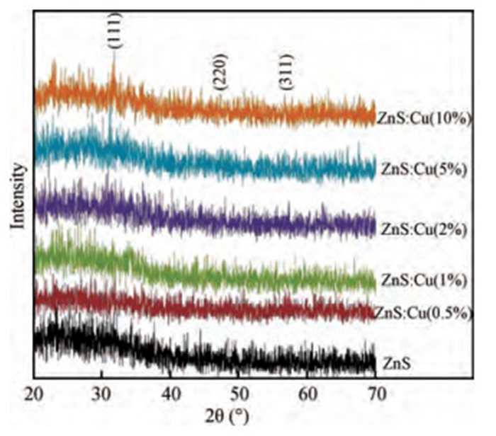
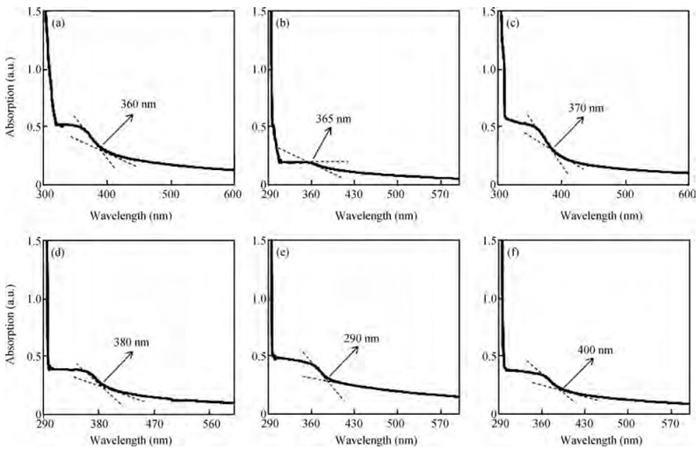
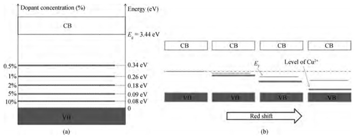
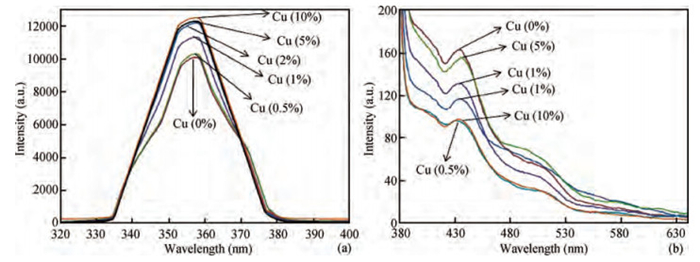
Un-doped and Cu-doped ZnS (ZnS:Cu) thin films were synthesized by Successive Ion Layer Absorption and Reaction (SILAR) method. The UV-visible absorption studies have been used to calculate the band gap values of the fabricated ZnS:Cu thin films. It was observed that by increasing the concentration of Cu2+ ions, the Fermi level moves toward the edge of the valence band of ZnS. Photoluminescence spectra of un-doped and Cu-doped ZnS thin films was recorded under 355 nm. The emission spectrum of samples has a blue emission band at 436 nm. The peak positions of the luminescence showed a red shift as the Cu2+ ion concentration was increased, which indicates that the acceptor level (of Cu2+) is getting close to the valence band of ZnS.

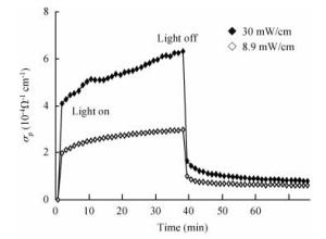
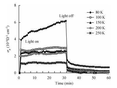
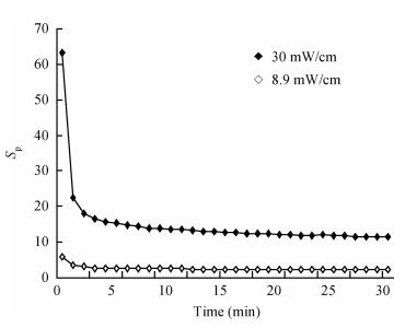
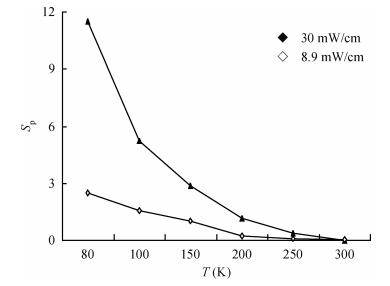
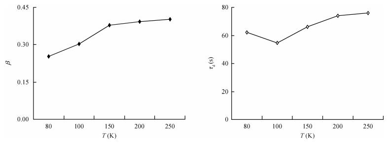
The persistent photoconductivity (PPC) of amorphous Hg0.78Cd0.22Te: In films has been studied under illumination by super-bandgap light (a He-Ne laser, hν=1.96 eV, 30 mW/cm2) and sub-bandgap light (1000 K Blackbody source, the largest photon energies hνp=0.42 eV, 8.9 mW/cm2) in the range of 80-300 K. The persistent photoconductivity effect increases with increase in illumination intensity and illumination time. However, it decreases with increase in working temperature. The non-exponential decay of photoconductivity implies the presence of continuous distribution of defect states in amorphous Hg0.78Cd0.22Te: In films. These results indicate that the decay of photoconductivity is not governed by the carrier trapped in the intrinsic defects, but it may be due to light-induced defects under light illumination.


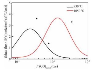
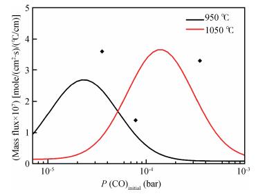
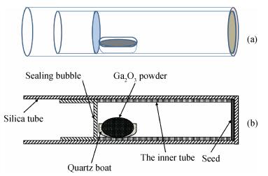
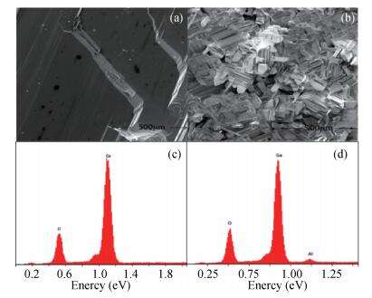
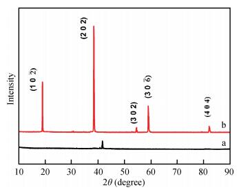
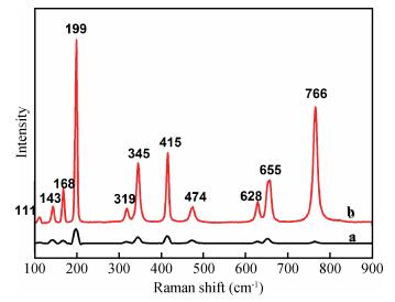
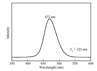
Beta-type gallium oxide (β-Ga2O3) is a new attractive material for optoelectronic devices. Different methods had been tried to grow high quality β-Ga2O3 crystals. In this work, crystal growth of Ga2O3 has been carried out by chemical vapor transport (CVT) method in a closed quartz tube using C as transport agent and sapphire wafer as seed. The CVT mass flux has been analyzed by theoretical calculations based on equilibrium thermodynamics and 1D diffusional mass transport. The crystal growth experimental results are in agreement with the theoretical predictions. Influence factors of Ga2O3 crystal growth, such as temperature distribution, amount of C as transport agent used, have also been discussed. Structural (XRD) and optical (Raman spectroscopy, photoluminescence spectrum) properties of the CVT-Ga2O3 crystal are presented.
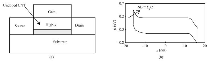
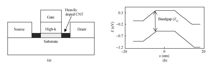
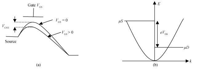
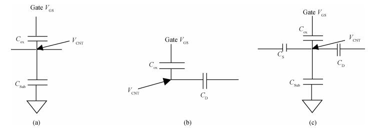
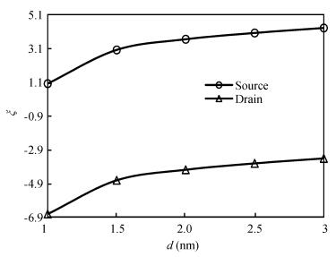
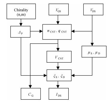
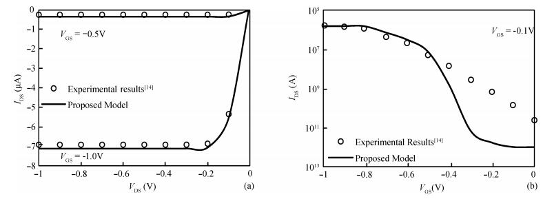
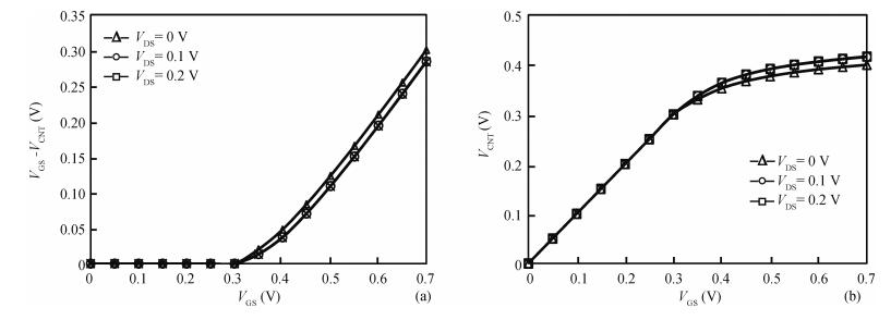
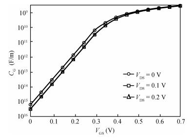
This paper proposes a compact model for carbon nanotube field effect transistor (CNTFET) based on surface potential and conduction band minima. The proposed model relates the I–V characteristics to chirality under quantum capacitance limit. C–V characteristics have been efficiently modelled for different capacitance models which are used to find the relationship between CNT surface potential and gate voltage. The role of different capacitances is discussed and it has been found that the proposed circuit compact model strictly follows quantum capacitance limit. The proposed model is efficiently designed for circuit simulations as it denies self-consistent numerical simulation. Furthermore, this compact model is compared with experimental results. The model has been used to simulate an inverter using HSPICE.
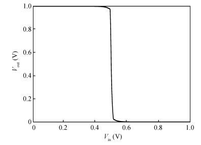
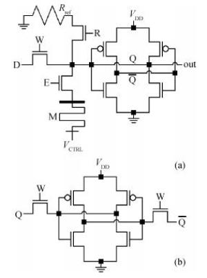
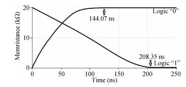
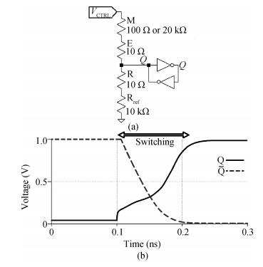
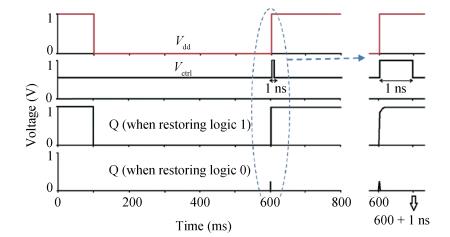
In this work, a novel memristive SRAM cell is designed using seven transistors and one memristor (7T1M). In this 7T1M SRAM cell, the non-volatile functionality is achieved by adding a single memristor and a transistor to the design of a volatile SRAM cell. The designing of the 7T1M SRAM cell also introduces VCTRL which allows bidirectional current flowing through the memristor, instead of relying on complementary input sources which would require more design components. In this article, memristive SRAM cells available from the literature are simulated using the same simulation environment for a fair comparison. Simulations show that the 7T1M SRAM cell has the least power consumption against other memristive SRAM cells in the literature. The 7T1M SRAM cell operates with an average switching speed of 176.21 ns and an average power consumption of 2.9665 μW. The 7T1M SRAM cell has an energy-delay-area product value of 1.61, which is the lowest among the memristive SRAM cells available in the literature.


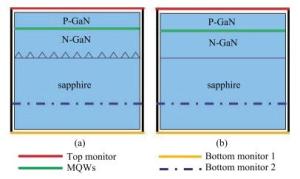
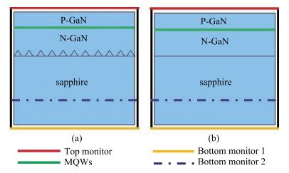
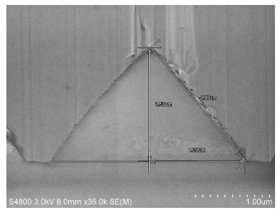
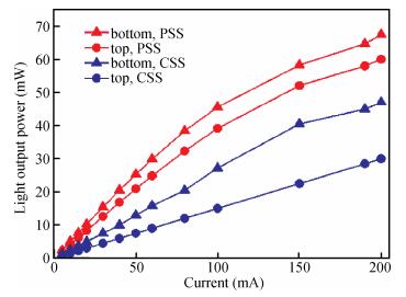
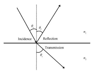
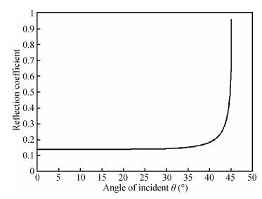
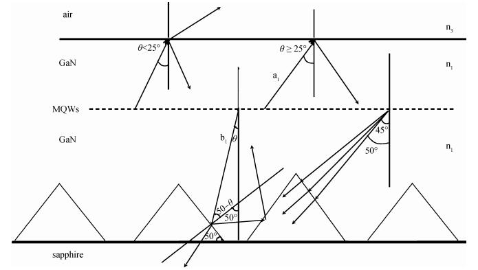
The effect of patterned sapphire substrate (PSS) on the top-surface (P-GaN-surface) and the bottom-surface (sapphire-surface) of the light output power (LOP) of GaN-based LEDs was investigated, in order to study the changes in reflection and transmission of the GaN-sapphire interface. Experimental research and computer simulations were combined to reveal a great enhancement in LOP from either the top or bottom surface of GaN-based LEDs, which are prepared on patterned sapphire substrates (PSS-LEDs). Furthermore, the results were compared to those of the conventional LEDs prepared on the planar sapphire substrates (CSS-LEDs). A detailed theoretical analysis was also presented to further support the explanation for the increase in both the effective reflection and transmission of PSS-GaN interface layers and to explain the causes of increased LOP values. Moreover, the bottom-surface of the PSS-LED chip shows slightly increased light output performance when compared to that of the top-surface. Therefore, the light extraction efficiency (LEE) can be further enhanced by integrating the method of PSS and flip-chip structure design.

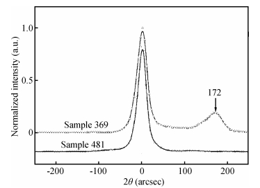
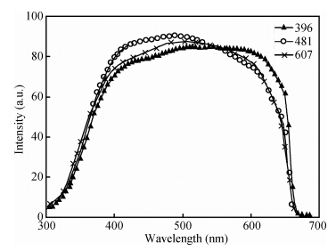
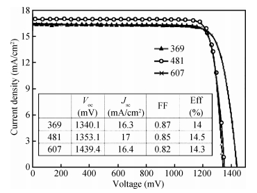
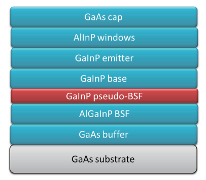
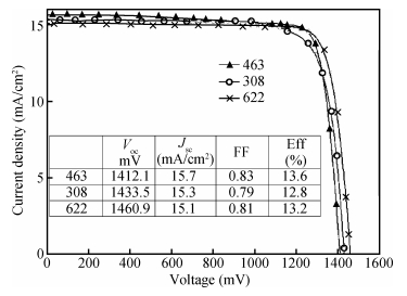
GaInP and AlGaInP solar cells were grown by metal organic chemical vapor deposition (MOCVD), and theoretical analysis demonstrated that hetero-interface recombination velocity plays an important role in the optimizing of cell performance, especially the interface between base layer and back surface field (BSF). Measurements including lattice-matched growth and pseudo-BSF were taken to optimize BSF design. Significant improvement of Voc in GaInP and AlGaInP solar cells imply that the measures we took are effective and promising for performance improvement in the next generation high efficiency solar cells.

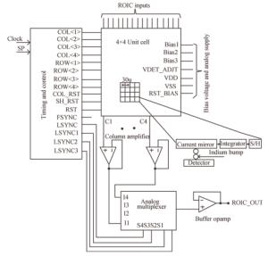
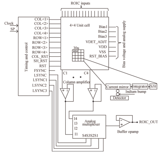
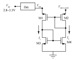
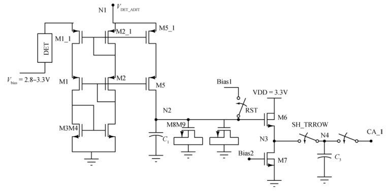
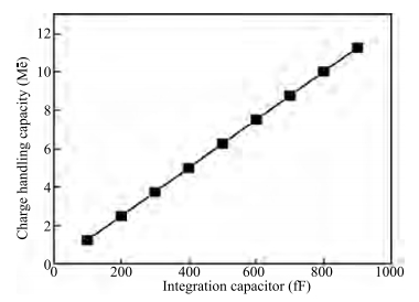
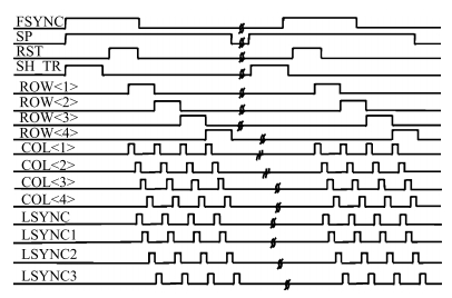
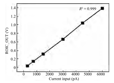
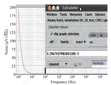
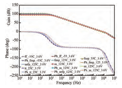
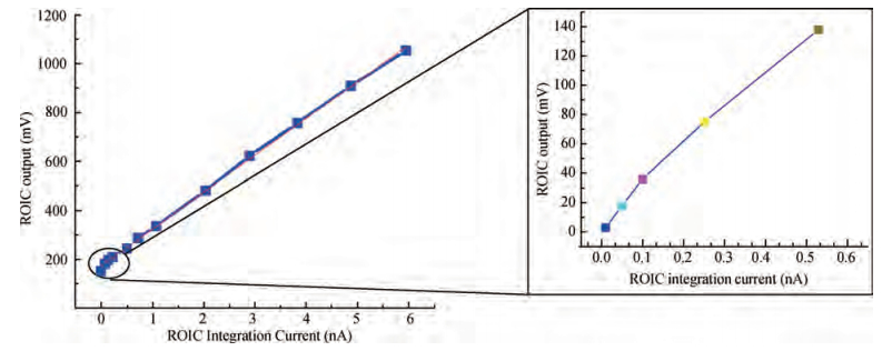
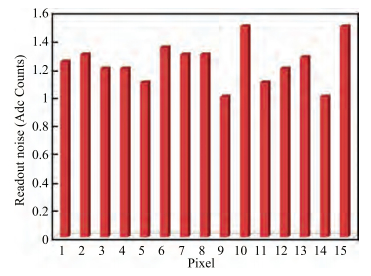
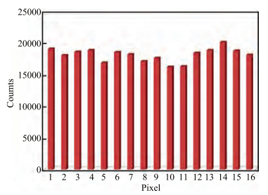
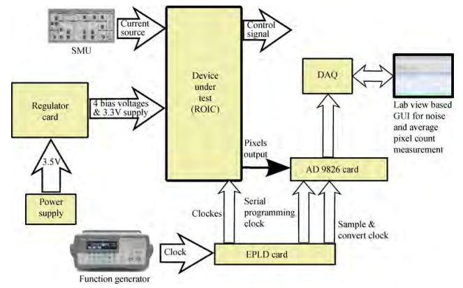
Current mirror integration (CMI) read out integrated circuit (ROIC) topology provides a low input impedance to photo-detectors and provides large injection efficiency, large charge handling capacity and snapshot mode operation without in-pixel opamps. The ROIC described in this paper has been implemented with a modified current mirror circuit, with matched PMOS pairs for detector input stage and its biasing. The readout circuit has been designed for 30×30μm2 pixel size, 4×4 array size, variable frame rate, 5 Mega pixel per second (Mpps). Experimental performance of the test chip has achieved 15 Me charge handling capacity, a high dynamic range of 83 dB, 99.8% linearity and 99.96% injection efficiency. The ROIC design has been fabricated in 3.3 V 1P6M UMC 180 nm CMOS process and tested up to 5 MHz pixel rate at room and at cryogenic temperature.


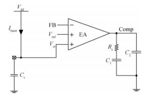
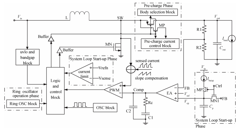
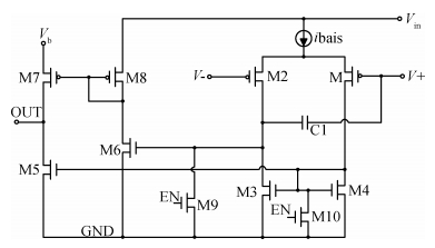
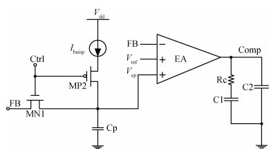
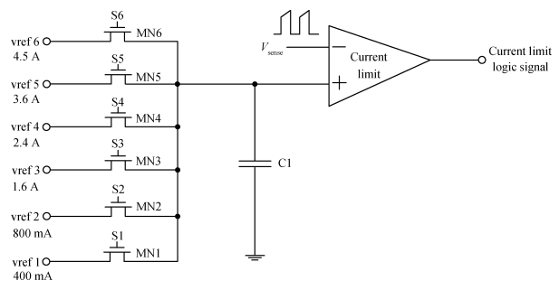
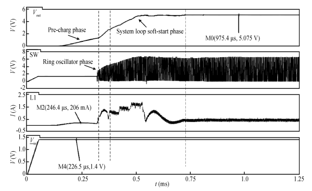
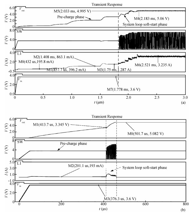
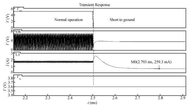
This paper presents a load adaptive soft-start scheme through which the inductor current of the synchronous boost DC-DC converter can trace the load current at the start-up stage. This scheme effectively eliminates the inrush-current and over-shoot voltage and improves the load capability of the converter. According to the output voltage, the start-up process is divided into three phases and at each phase the inductor current is limited to match the load. In the pre-charge phase, a step-increasing constant current gives a smooth rise of the output voltage which avoids inrush current and ensures the converter successfully starts up at different load situations. An additional ring oscillator operation phase enables the converter to start up as low as 1.4 V. When the converter enters into the system loop soft-start phase, an output voltage and inductor current detection methods make the transition of the phases smooth and the inductor current and output voltage rise steadily. Effective protection circuits such as short-circuit protection, current limit circuit and over-temperature protection circuit are designed to guarantee the safety and reliability of the chip during the start-up process. The proposed start-up circuit is implemented in a synchronous boost DC-DC converter based on TSMC 0.35μm CMOS process with an input voltage range 1.4-4.2 V, and a steady output voltage 5 V, and the switching frequency is 1 MHz. Simulation results show that inrush current and overshoot voltage are suppressed with a load range from 0-2.1 A, and inductor current is as low as 259 mA when the output shorts to the ground.


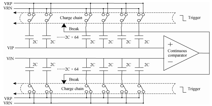
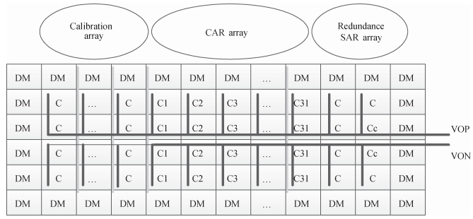
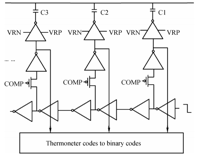
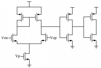
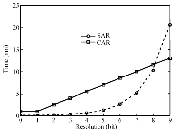
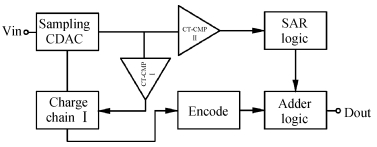
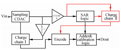
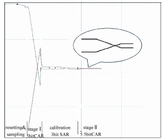
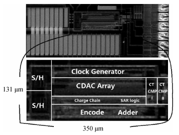
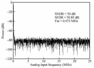
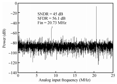
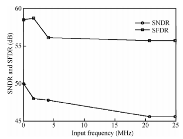
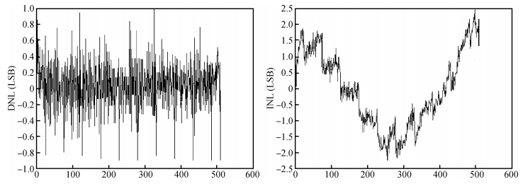
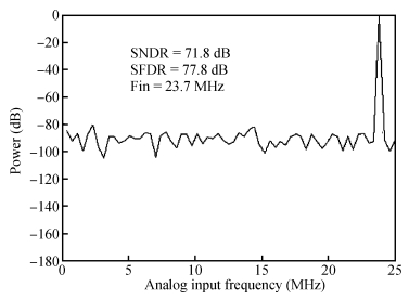
A 9 bits 50 MS/s 0.5 mW continuous approximation mixed successive approximation (CAR&SAR) ADC is presented. A 12 bits 50 MS/s 0.6 mW CAR&CAR ADC is presented. In the field of low power and high performance ADC, CAR is a new architecture different from SAR. It is faster and easier to get high accuracy. Here we will introduce CAR and its circuit implementation, and the 9 bits experimental ADC is designed to verify CARADC's feasibility. Meanwhile, its resolution can be extended to 12 bits with adding an extra CAR, and then the performance is raised to 0.6 mW 50 MS/s 72 dB SNDR at TT corner and the Walden FOM is 3.6 fj/conv-step. The 9 b ADC was fabricated by using TSMC 1P9M 65 nm CMOS technology. The ADC achieves 50 dB SNDR and the realized Walden FOM is 34 fj/conv-step. The simulation and measurement results prove that CAR is available in the low power and high performance ADC and it even outperforms SAR. The ADC core occupies an active area of 0.045 mm2.


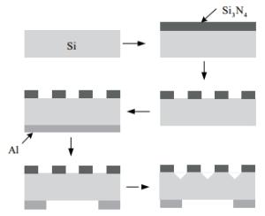
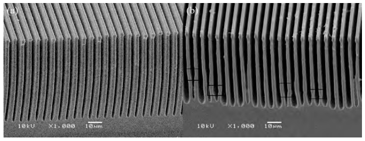
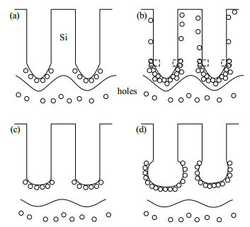
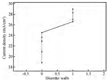
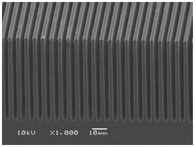
The fabrication of ordered, high aspect-ratio microstructures in silicon by use of photo-assisted electrochemical etching is an important technology, where voltage and current density are significant factors. In this paper, disordered walls appear in 5-inch n-type silicon wafers when a large current density is used. Based on the theory of space charge region, these disordered walls are caused by the contradiction between the protection from dissolution by a high applied voltage and the dissolution by a high current density. To verify this point, wall arrays were fabricated at different applied voltages and current densities. Moreover, the critical voltage was kept constant and different current densities were applied to obtain conditions for avoiding disordered walls and achieving uniform wall arrays. Finally, a wall array with a period of 5.6μm and a depth of 55μm was achieved at an applied voltage of 3 V and a monotonically increasing current density ranging from 22.9 to 24.5 mA/cm2.

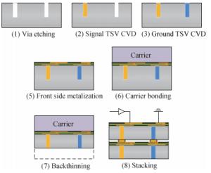
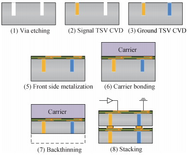
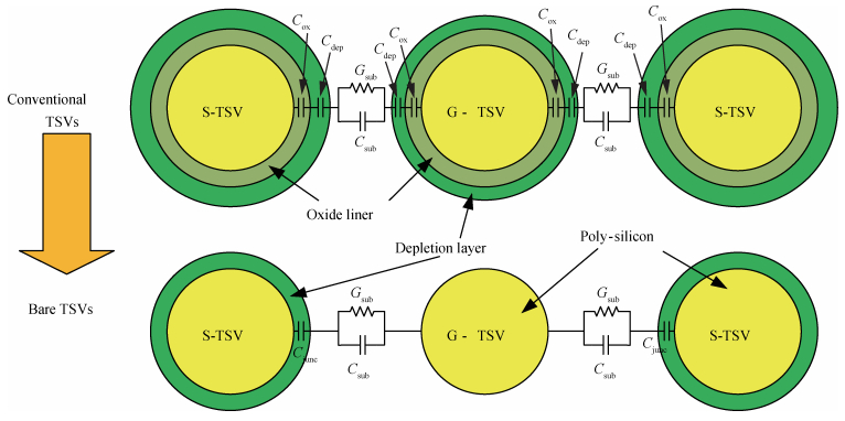
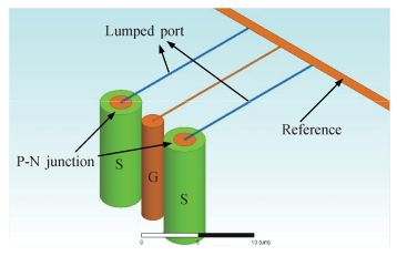
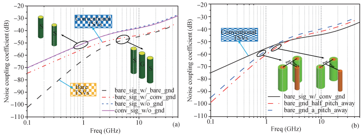
In this paper, a new type of through-silicon via (TSV) for via-first process namely bare TSV, is proposed and analyzed with the aim of mitigating noise coupling problems in 3D integrated systems for advanced technology nodes. The bare TSVs have no insulation layers, and are divided into two types: bare signal TSVs and bare ground TSVs. First, by solving Poisson's equation for cylindrical P-N junctions, the bare signal TSVs are shown to be equivalent to conventional signal TSVs according to the simulation results. Then the bare ground TSV is proved to have improved noise-absorption capability when compared with a conventional ground TSV. Also, the proposed bare TSVs offer more advantages to circuits than other noise isolation methods, because the original circuit design, routing and placement can be retained after the application of the bare TSVs.