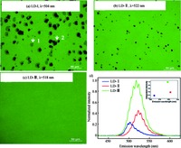
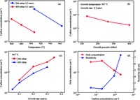
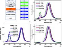
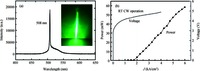
Recently, many groups have focused on the development of GaN-based green LDs to meet the demand for laser display. Great progresses have been achieved in the past few years even that many challenges exist. In this article, we analysis the challenges to develop GaN-based green LDs, and then the approaches to improve the green LD structure in the aspect of crystalline quality, electrical properties, and epitaxial layer structure are reviewed, especially the work we have done.
Issue Browser
Volume 37, Issue 11,
Nov 2016


J. Semicond.
2016, 37(11): 112001 doi: 10.1088/1674-4926/37/11/112001
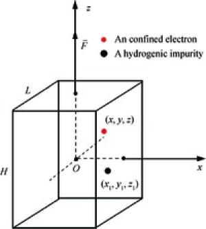
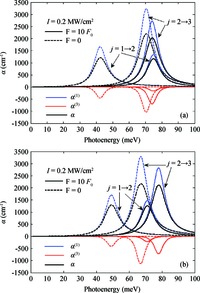
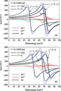
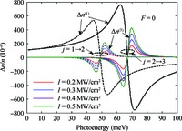
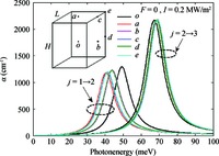
Within the quasi-one-dimensional effective potential model and effective mass approximation, we obtain the wavefunctions and energy eigenvalues of the ground (j=1) and first 2 excited states (j=2 and 3) of a donor impurity in a rectangular GaAs quantum dot in the presence of electric field. The donor impurity-related linear and nonlinear optical absorption as well as refractive index changes for the transitions j=1-2 and j=2-3 are investigated. The results show that the impurity position, incident optical intensity and electric field play important roles in the optical absorption coefficients and refractive index changes. We find that the impurity effect induces the blueshift for j=1-2 and redshift for j=3-2 in the absence of the electric field, but it leads to redshift for j=1-2 and blueshift for j=3-2 in the existence of the field. Also, the optical coefficient for the higher energy transitions j=2-3 is insensitive to variation of impurity positions, while that for the low energy transition j=1-2 depends significantly on the positions of impurity. In addition, the saturation and splitting phenomenon of the optical absorption are observed as the incident optical intensity increases.


J. Semicond.
2016, 37(11): 113001 doi: 10.1088/1674-4926/37/11/113001

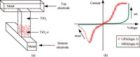
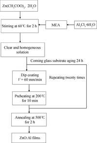
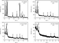
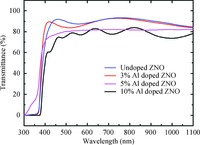
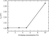
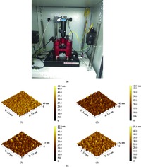
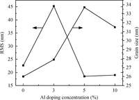
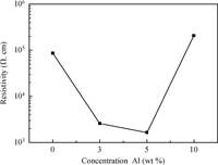
In this work, sol-gel dip-coating technique was used to elaborate ZnO pure and ZnO/Al films. The impact of Al-doped concentration on the structural, optical, surface morphological and electrical properties of the elaborated samples was investigated. It was found that better electrical and optical performances have been obtained for an Al concentration equal to 5%, where the ZnO thin films exhibit a resistivity value equal to 1.64104 Ω·cm. Moreover, highest transparency has been recorded for the same Al concentration value. The obtained results from this investigation make the developed thin film structure a potential candidate for high optoelectronic performance applications.
J. Semicond.
2016, 37(11): 113002 doi: 10.1088/1674-4926/37/11/113002

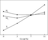
Cobalt-doped ZnO powder samples were prepared by sol-gel and hydrothermal method combined. The prepared powder samples were characterized by X-ray diffraction (XRD), scanning electron microscopy (SEM), electron paramagnetic resonance (EPR) and vibrating sample magnetometry (VSM). XRD patterns show that all the samples have a single pure phase with wurtzite structure suggesting that Co2+ occupied Zn2+ sites in the ZnO crystal lattice. SEM images show that crystal grains of cobalt-doped ZnO are hexagonal cone or spheroidal. EPR pattern shows that all of the samples possess oxygen vacancy. Measurement of magnetism indicates that all the samples exhibit room temperature ferromagnetism (RTFM) embedded in a dominant diamagnetic or paramagnetic signal. The dominant signal turns from diamagnetic to paramagnetic with the increase of Co concentration. The magnetic behavior can attribute to defects and Co doping.

J. Semicond.
2016, 37(11): 114001 doi: 10.1088/1674-4926/37/11/114001

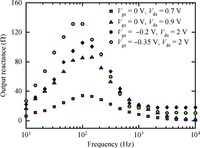
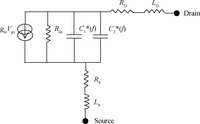
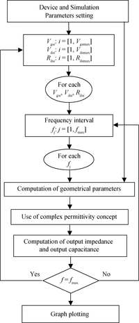
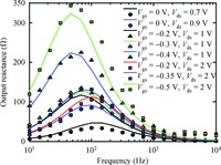
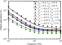
The aim of this article is to investigate the effect of dielectric loss tangent on frequency dispersion of output reactance and capacitance in GaAs MESFETs. For this purpose, measurements of output impedance modulus and phase have been carried out within a frequency range of 10 Hz to 10 kHz, and various voltage values of gate-source (Vgs=0, -0.2, -0.3, -0.35, -0.4, -0.45, -0.5 and -0.6 V) and drain-source (Vds=0.7, 0.9, 1, 1.5 and 2 V) Based on the concept of complex permittivity of semiconductor material, complex capacitance is used to analyze and simulate frequency dispersion of output reactance and capacitance of GaAs MESFETs. The results show that conductor losses which dominate the dielectric loss tangent are attributed to trapping mechanisms at the interface of devices; so they influence the frequency dispersion of output reactance and capacitance in particular at low frequencies. This reveals that frequency dispersion of these parameters is also related to dielectric loss tangent of semiconductor materials which affects the response of electronic devices according to frequency variation.
J. Semicond.
2016, 37(11): 114002 doi: 10.1088/1674-4926/37/11/114002
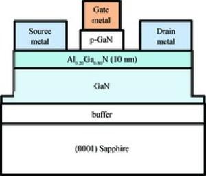
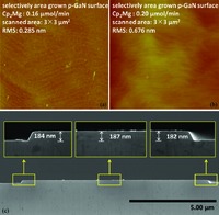
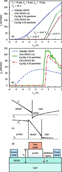
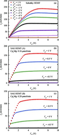
We report a selective area growth (SAG) method to define the p-GaN gate of AlGaN/GaN high electron mobility transistors (HEMTs) by metal-organic chemical vapor deposition. Compared with Schottky gate HEMTs, the SAG p-GaN gate HEMTs show more positive threshold voltage (Vth) and better gate control ability. The influence of Cp2Mg flux of SAG p-GaN gate on the AlGaN/GaN HEMTs has also been studied. With the increasing Cp2Mg from 0.16 μmol/min to 0.20 μmol/min, the Vth raises from -67 V to -37 V. The maximum transconductance of the SAG HEMT at a drain voltage of 10 V is 113.9 mS/mm while that value of the Schottky HEMT is 51.6 mS/mm. The SAG method paves a promising way for achieving p-GaN gate normally-off AlGaN/GaN HEMTs without dry etching damage.

J. Semicond.
2016, 37(11): 114003 doi: 10.1088/1674-4926/37/11/114003
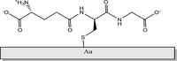
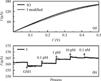
Lead poisoning is a serious environmental concern, which is a health threat. Existing technologies always have some drawbacks, which restrict their application ranges, such as real time monitoring. To solve this problem, glutathione was functionalized on the Au-coated gate area of the pseudomorphic high electron mobility transistor (pHEMT) to detect trace amounts of Pb2+. The positive charge of lead ions will cause a positive potential on the Au gate of the pHEMT sensor, which will increase the current between the source and the drain. The response range for Pb2+ detection has been determined in the concentrations from 0.1 pmol/L to 10 pmol/L. To our knowledge, this is currently the best result for detecting lead ions.

J. Semicond.
2016, 37(11): 114004 doi: 10.1088/1674-4926/37/11/114004
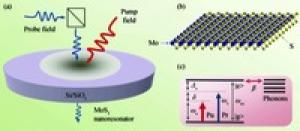
Atomically thin two-dimensional semiconductor nanomaterials have attained considerable attention currently. Here, we present a nano-optomechanical system based on a suspended monolayer molybdenum disulfide (MoS2). The linear and nonlinear coherent optical properties of this system, and the phenomenon of phonon-induced transparency are demonstrated. The transmission of the probe field can be manipulated by the power of a second ‘gating' (pump) field, which indicates a promising candidate for an optical transistor. We further study the nonlinear effect of the system, and the optical Kerr effect of the monolayer MoS2 resonator can be regulated under different parameter regimes. This scheme proposed here may indicate potential chip-scale applications of monolayer MoS2 resonator in quantum information with the currently popular pump-probe technology.


J. Semicond.
2016, 37(11): 114005 doi: 10.1088/1674-4926/37/11/114005
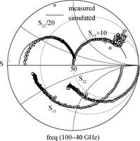
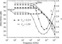
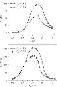
A 3D model simulation of InP/InGaAs/InP DHBT is reported in this paper. A comprehensive set of built-in physical models are described, including Stratton's hydrodynamic model, high-fields mobility model and thermionic emission model. A mixed-mode environment is required for AC simulation instead of simulating an isolated HBT, in which the HBT is embedded in an external circuit, and the circuit voltage and current equations are solved along with the Poisson equation and transport equations. In AC simulation, simulator Sentaurus provides the computation of the small signal admittance Y matrix. From the results of Y matrix, the small signal equivalent circuit is constructed with the conductance and capacitance obtained from Y matrix, and the AC parameters, such as S-parameters, will be calculated. The small signal AC characteristics of InP/InGaAs DHBTs under proton irradiation are simulated with different fluences of proton irradiation. Simulation results show that the maximum oscillation frequency will be degraded when fluence of proton irradiation is increased.
J. Semicond.
2016, 37(11): 114006 doi: 10.1088/1674-4926/37/11/114006
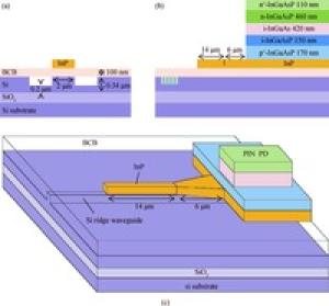
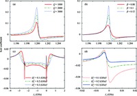
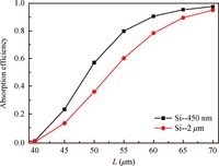
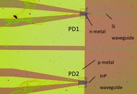
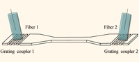
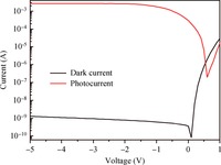
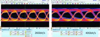
This paper presents a high-responsivity and high-speed InGaAs/InP PIN photodetector integrated onto the silicon waveguide substrate utilizing the divinyltetramethyldisiloxane-benzocyclobutene (DVS-BCB) adhesive bonding method. A grating coupler is adopted to couple light from the fiber to the silicon waveguide. Light in the silicon photonic waveguide is evanescently coupled into the photodetector. The integrated photodetector structure is first simulated using the FDTD (finite difference time domain) solutions software and the simulation results show a detection efficiency of 95%. According to the simulation result, the integrated photodetector is fabricated. The measured responsivity of the fabricated integrated photodetector with a detection length of 30 μm is 0.89 A/W excluding the coupling loss between the fiber and the grating coupler and the silicon propagation loss at the wavelength of 1550 nm with a reverse bias voltage of 3 V. Measured 3-dB bandwidth is 27 GHz using the Lightwave Component Analyzer (LCA). The eye diagram signal test results indicate that the photodetector can operate at a high speed of 40 Gbit/s. The integrated photodetector is of great significance in the silicon-based optoelectronic integrated chip which can be applied to the optical communication and the super node data transmission chip of the high-performance computer.


J. Semicond.
2016, 37(11): 114007 doi: 10.1088/1674-4926/37/11/114007

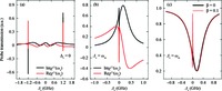
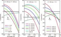
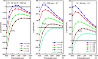
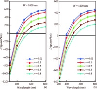
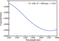
We investigate the dispersion properties of nanometer-scaled silicon nitride suspended membrane waveguides around the communication wavelength and systematically study their relationship with the key structural parameters of the waveguide. The simulation results show that a suspended membrane waveguide can realize anomalous dispersion with a relatively thinner silicon nitride thickness in the range of 400 to 600 nm, whereas, for the same membrane thickness, a conventional rib or strip silicon nitride waveguide cannot support anomalous dispersion. In particular, a waveguide with 400 nm silicon nitride thickness and deep etch depth (r=0.05) exhibits anomalous dispersion around the communication wavelength when the waveguide width ranges from 990 to 1255 nm, and the maximum dispersion is 22.56 ps/(nm·km). This specially designed anomalous dispersion silicon nitride waveguide is highly desirable for micro-resonator based optical frequency combs due to its potential to meet the phase-matching condition required for cascaded four-wave-mixing.


J. Semicond.
2016, 37(11): 114008 doi: 10.1088/1674-4926/37/11/114008
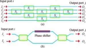
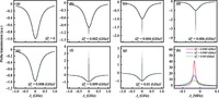
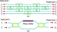
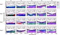
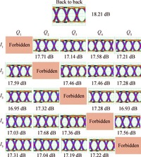
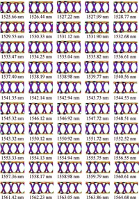
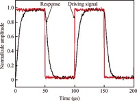
With the continuous development of integrated circuits, the performance of the processor has been improved steadily. To integrate more cores in one processor is an effective way to improve the performance of the processor, while it is impossible to further improve the property of the processor by only increasing the clock frequency. For a processor with integrated multiple cores, its performance is determined not only by the number of cores, but also by communication efficiency between them. With more processor cores integrated on a chip, larger bandwidths are required to establish the communication among them. The traditional electrical interconnect has gradually become a bottleneck for improving the performance of multiple-core processors due to its limited bandwidth, high power consumption, and long latency. The optical interconnect is considered as a potential way to solve this issue. The optical router is the key device for realizing the optical interconnect. Its basic function is to achieve the data routing and switching between the local node and the multi-node. In this paper we present a five-port optical router for Mesh photonics network-on-chip. A five-port optical router composed of eight thermally tuned silicon Mach-Zehnder optical switches is demonstrated. The experimental spectral responses indicate that the optical signal-to-noise ratios of the optical router are over 13 dB in the wavelength range of 1525-1565 nm for all of its 20 optical links. Each optical link can manipulate 50 wavelength channels with the channel spacing of 100 GHz and the data rate of 32 Gbps for each wavelength channel in the same wavelength range. The lowest energy efficiency of the optical router is 43.4 fJ/bit.


J. Semicond.
2016, 37(11): 115001 doi: 10.1088/1674-4926/37/11/115001

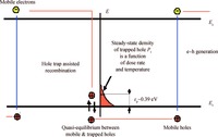
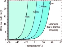
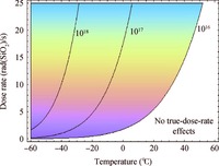
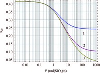
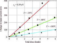
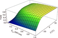
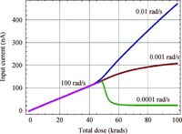
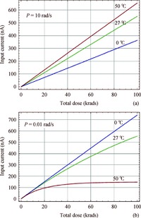
This paper describes an approach to prediction of the thick insulators' radiation response based on modeling of the charge yield, which is dependent on irradiation temperature, dose rate, and electric field magnitudes. Temperature behavior of the charge yield and degradation saturation due to the interface precursor depletion has been modeled and simulated. Competition between the time-dependent and true dose rate (ELDRS) effects has been simulated and discussed within a framework of the rate-equation-based mathematical model. It was shown that the precursor trap in the thick insulating oxides can be important at high dose rates. It was also shown that full filling of the shallow hole traps in the insulating oxide bulk can cause suppression of dose-rate sensitivity at relatively high dose rates, especially in thick insulators.
J. Semicond.
2016, 37(11): 115002 doi: 10.1088/1674-4926/37/11/115002

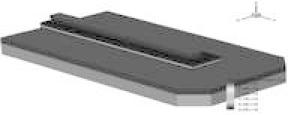
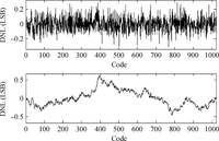
A readout integrated circuit (ROIC) for a MEMS (microelectromechanical system)-array-based focal plane (MAFP) intended for imaging applications is presented. The ROIC incorporates current sources for diode detectors, scanners, timing sequence controllers, differential buffered injection-capacitive trans-impedance amplifier (DBI-CTIA) and 10-bit cyclic ADCs, and is integrated with MAFP using 3-D integration technology. A small-signal equivalent model is built to include thermal detectors into circuit simulations. The biasing current is optimized in terms of signal-to-noise ratio and power consumption. Layout design is tailored to fulfill the requirements of 3-D integration and to adapt to the size of MAFP elements, with not all but only the 2 bottom metal layers to complete nearly all the interconnections in DBI-CTIA and ADC in a 40 μm wide column. Experimental chips are designed and fabricated in a 0.35 μm CMOS mixed signal process, and verified in a code density test of which the results indicate a (0.29/-0.31) LSB differential nonlinearity (DNL) and a (0.61/-0.45) LSB integral nonlinearity (INL). Spectrum analysis shows that the effective number of bits (ENOB) is 9.09. The ROIC consumes 248 mW of power at most if not to cut off quiescent current paths when not needed.


J. Semicond.
2016, 37(11): 115003 doi: 10.1088/1674-4926/37/11/115003

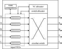
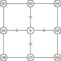
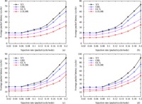
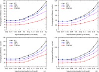
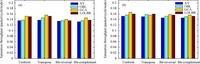
The design of a router in a network-on-chip (NoC) system has an important impact on some performance criteria. In this paper, we propose a low overhead load balancing router (LOLBR) for 2D mesh NoC to enhance routing performance criteria with low hardware overhead. The proposed LOLBR employs a balance toggle identifier to control the initial routing direction of X or Y for flit injection. The simplified demultiplexers and multiplexers are used to handle output ports allocation and contention, which provide a guarantee of deadlock avoidance. Simulation results show that the proposed LOLBR yields an improvement of routing performance over the reported routing schemes in average packet latency by 26.5%. The layout area and power consumption of the network compared with the reported routing schemes are 15.3% and 11.6% less respectively.

J. Semicond.
2016, 37(11): 115004 doi: 10.1088/1674-4926/37/11/115004

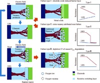
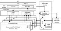
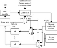
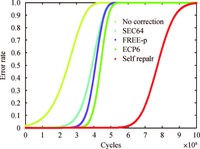
Resistive random access memory (RRAM) is one of the promising candidates for future universal memory. However, it suffers from serious error rate and endurance problems. Therefore, exploring a technical solution is greatly demanded to enhance endurance and reduce error rate. In this paper, we propose a reliable RRAM architecture that includes two reliability modules: error correction code (ECC) and self-repair modules. The ECC module is used to detect errors and decrease error rate. The self-repair module, which is proposed for the first time for RRAM, can get the information of error bits and repair wear-out cells by a repair voltage. Simulation results show that the proposed architecture can achieve lowest error rate and longest lifetime compared to previous reliable designs.