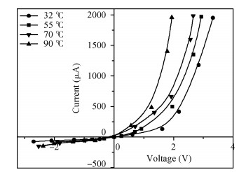
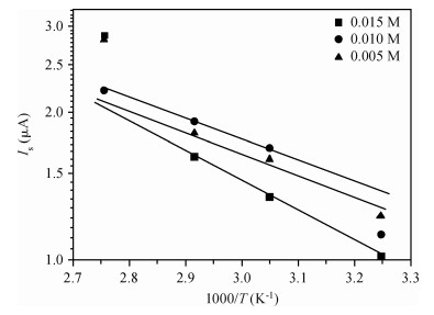
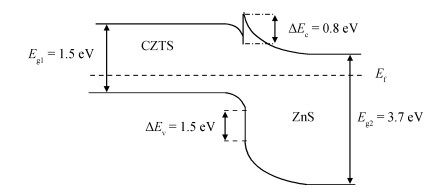
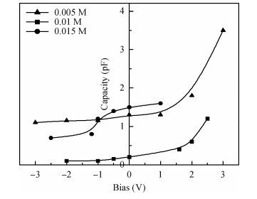
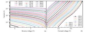
Cu2ZnSnS4 (CZTS)/ZnS heterojunctions have been prepared by a successive deposition of ZnS and CZTS thin films by ultrasonic spray pyrolysis technique on glass substrates. The cupric chloride concentration has been varied in the starting solution in order to investigate its influence on device properties. CZTS/ZnS heterojunctions were characterized by recording their current-voltage characteristics at different temperatures. The obtained results exhibit a good rectifying behavior of the realized heterojunction. Analysis of these results yields saturation current, series resistance and ideality factor determination. From the activation energy of saturation current we inferred that the thermal emission through the barrier height is the dominant mechanism of the reverse current rather than the defects contribution.


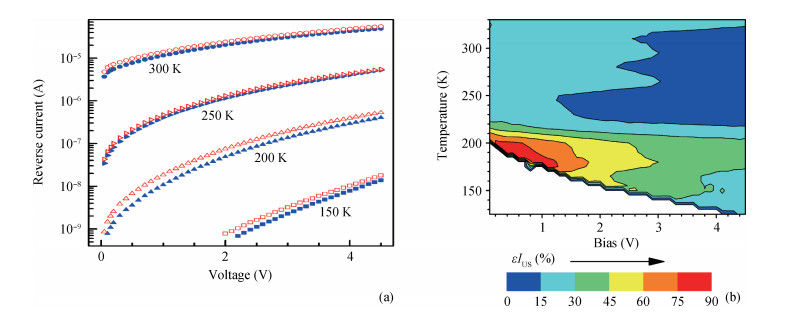
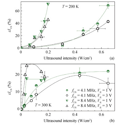
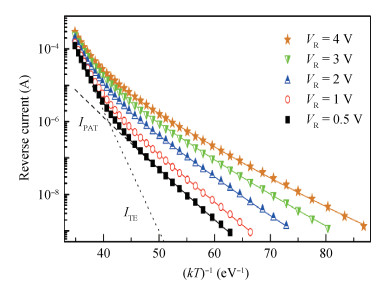
The influence of ultrasonic loading on reverse current-voltage characteristics of Mo/n-n+-Si structures has been investigated. The research of leakage current variation has been carried out for various ultrasonic wave frequencies (4.1 and 8.4 MHz), intensities (up to 0.8 W/cm2) and loading temperatures (130-330 K). The observed reversible acoustically induced increase in reverse currents was as large as 60%. It has been found that dominant charge transfer mechanisms are the thermionic emission (at high temperature) and the phonon-assisted tunneling (at low temperature). The ultrasound loading affects both processes due to the decrease of Schottky barrier height and binding energy of the electron on the trap.


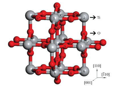
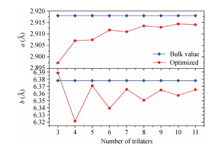
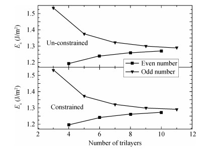
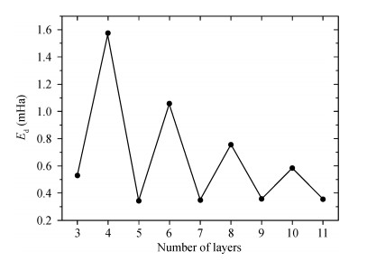
Traditionally, we use a slab to mimic a surface and we constrain the slab to have the bulk-terminated 2D lattice constants. Here we propose a different model in which we impose no constraints, allowing all coordinates including the 2D slab itself to relax. We perform DFT calculations on both models. We find that the unconstrained slabs yield better agreement with experimental results and they have lower total energies. The optimized 2D lattice constants of the unconstrained slabs eventually converge to the attached bulk value. The total energy difference reveals that, with odd number trilayers, the unconstrained slab is much closer to the corresponding constrained slab. The surface energies both converge to the individual values with the number of atomic layers.

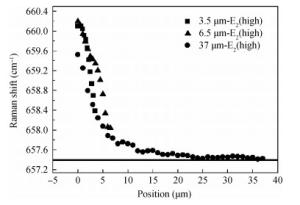
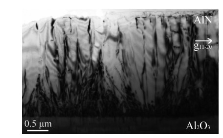
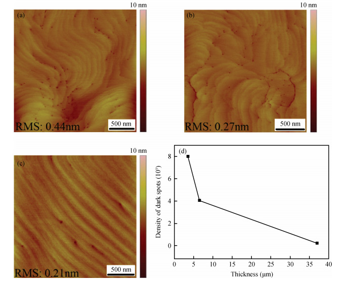
AlN thick films were grown on c-plane sapphire substrates by hydride vapor phase epitaxy at high temperature. The evolution of the strain state and crystal quality of AlN with increase of thickness were investigated by transmission electron microscopy, field-emission scanning electron microscopy, Raman spectra and atomic force microscopy (AFM). As the thickness increased, the stress in the epilayers decreased gradually, which was attributed to the reaction of dislocations at the first several microns in thickness. When the thickness was more than 20 μm, the stress was almost fully relaxed due to the formation of cracks. Wet etching experiments indicated that the dislocation density decreased with the increase of thickness. The AFM images showed that the density of dark spots on the surface obviously decreased and the atomic steps became straight as the thickness increased.

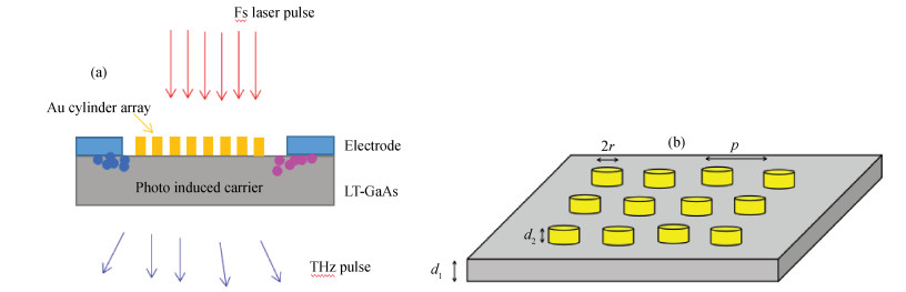
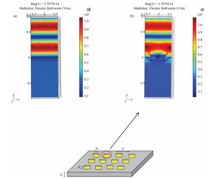
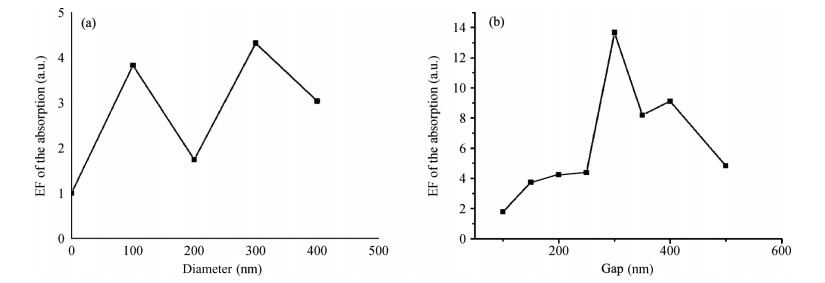
Photoconductive antennas (PCAs) based on nanoplasmonic gratings contact electrodes have been proposed to satisfy the demand for high power, efficiency and responsivity terahertz (THz) sources. Reducing the average photo-generated carrier transport path to the photoconductor contact electrodes was previously considered the dominant mechanism to improve PCAs' power. However, considering the bias in a real device, the electric field between gratings is limited and the role of surface plasmonic resonance (SPR) field enhancement is more important in improving THz radiation. This paper, based on SPR, analyzes the interaction between incident light and substrate in nano cylinder array PCAs and clearly shows that the SPR can enhance the light absorption in the substrate. After the optimization of the structure size, the proposed structure can offer 87% optical transmission into GaAs substrate. Compared with conventional PCAs, the optical transmission into the substrate will increase 5.8 times and the enhancement factor of substrate absorption will reach 13.7 respectively.
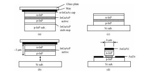
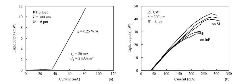
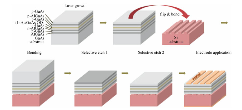
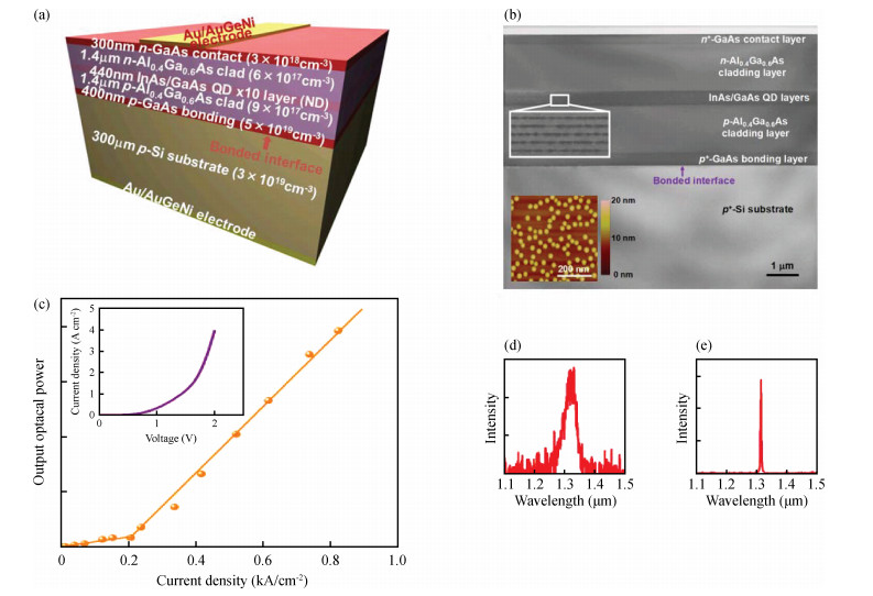
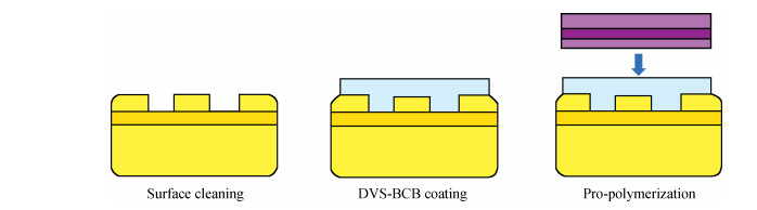
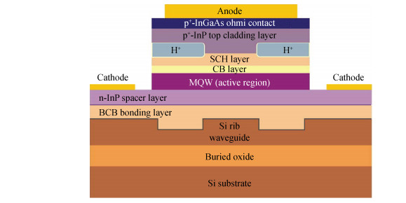
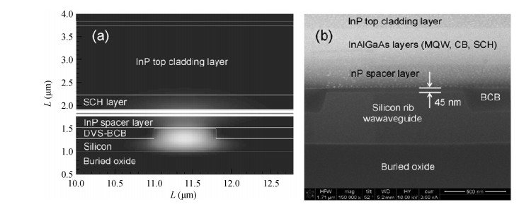
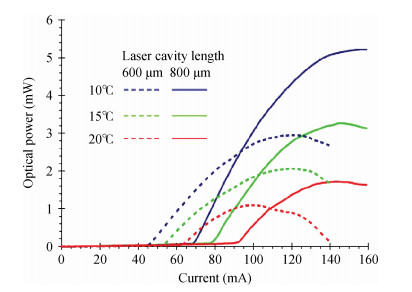
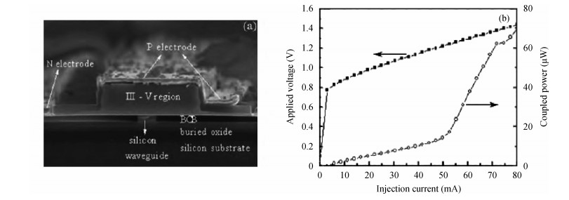
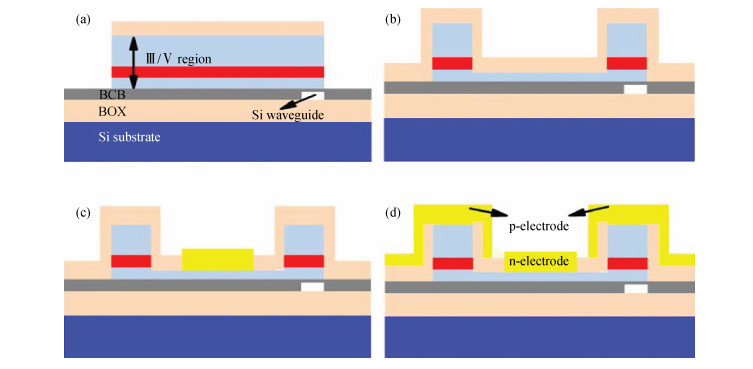
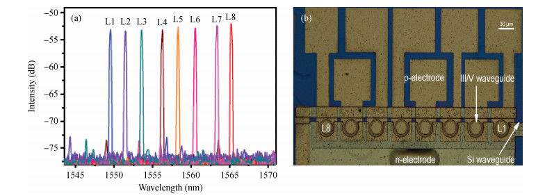
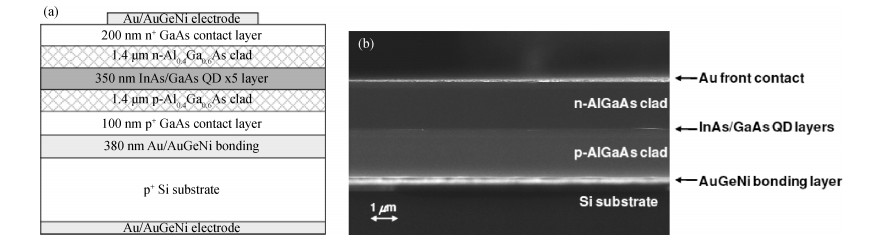
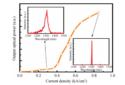
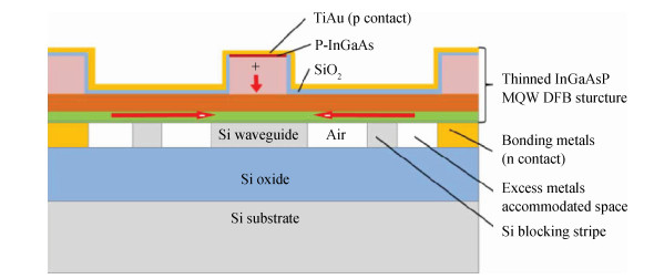
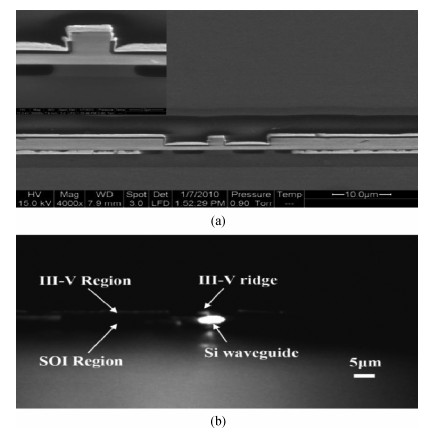
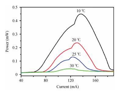
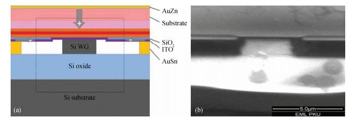
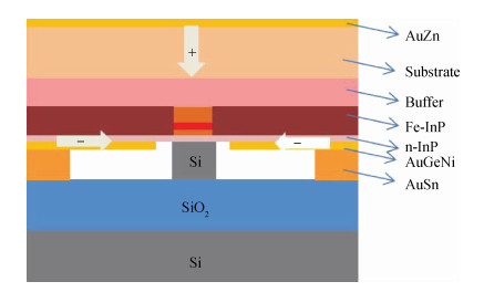
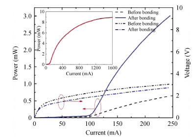
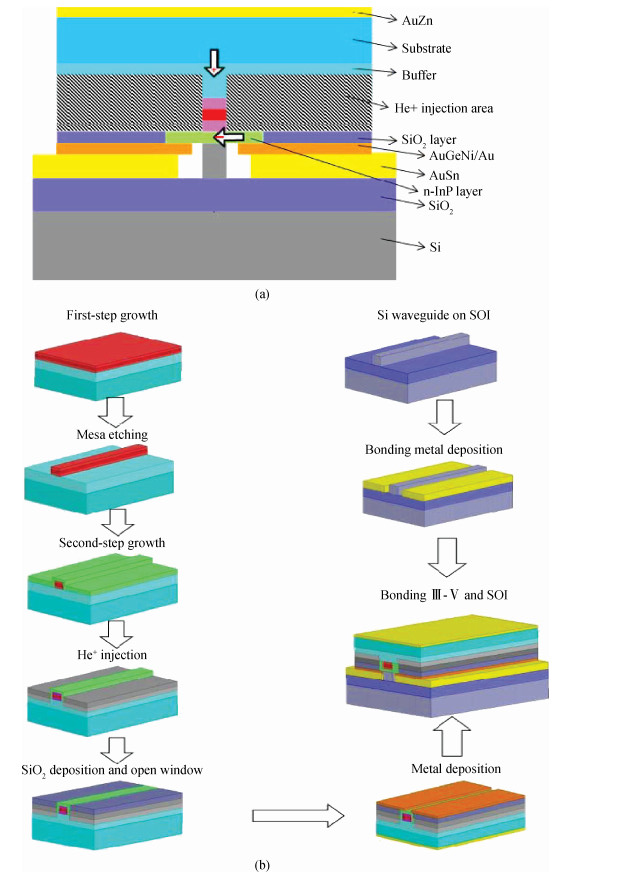
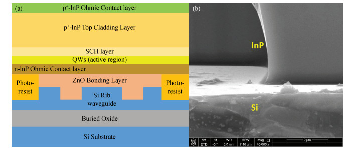
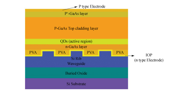
The vigorous development of silicon photonics makes a silicon-based light source essential for optoelectronics' integration. Bonding of Ⅲ-Ⅴ/Si hybrid laser has developed rapidly in the last ten years. In the tireless efforts of researchers, we are privileged to see these bonding methods, such as direct bonding, medium adhesive bonding and low temperature eutectic bonding. They have been developed and applied to the research and fabrication of Ⅲ-Ⅴ/Si hybrid lasers. Some research groups have made remarkable progress. Tanabe Katsuaki of Tokyo University successfully implemented a silicon-based InAs/GaAs quantum dot laser with direct bonding method in 2012. They have bonded the InAs/GaAs quantum dot laser to the silicon substrate and the silicon ridge waveguide, respectively. The threshold current of the device is as low as 200 A/cm2. Stevan Stanković and Sui Shaoshuai successfully produced a variety of hybrid Ⅲ-Ⅴ/Si laser with the method of BCB bonding, respectively. BCB has high light transmittance and it can provide high bonding strength. Researchers of Tokyo University and Peking University have realized Ⅲ-Ⅴ/Si hybrid lasers with metal bonding method. We describe the progress in the fabrication of Ⅲ-Ⅴ/Si hybrid lasers with bonding methods by various research groups in recent years. The advantages and disadvantages of these methods are presented. We also introduce the progress of the growth of III-V epitaxial layer on silicon substrate, which is also a promising method to realize silicon-based light source. I hope that readers can have a general understanding of this field from this article and we can attract more researchers to focus on the study in this field.

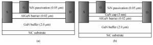
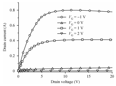
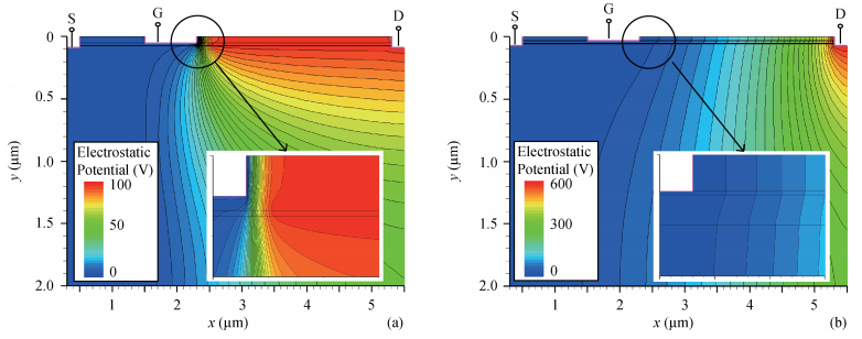
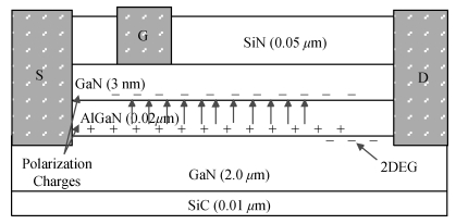
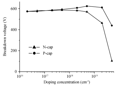
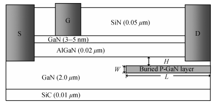
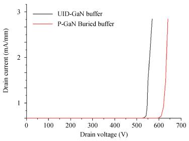
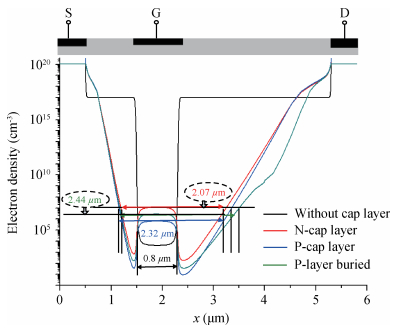
Simulations are carried out to explore the possibility of achieving high breakdown voltage of GaN HEMT (high-electron mobility transistor). GaN cap layers with gradual increase in the doping concentration from 2×10¹⁶ to 5×1019 cm-3 of N-type and P-type cap are investigated, respectively. Simulation results show that HEMT with P-doped GaN cap layer shows more potential to achieve higher breakdown voltage than N-doped GaN cap layer under the same doping concentration. This is because the ionized net negative space charges in P-GaN cap layer could modulate the surface electric field which makes more contribution to RESURF effect. Furthermore, a novel GaN/AlGaN/GaN HEMT with P-doped GaN buried layer in GaN buffer between gate and drain electrode is proposed. It shows enhanced performance. The breakdown voltage of the proposed structure is 640 V which is increased by 12% in comparison to UID (un-intentionally doped) GaN/AlGaN/GaN HEMT. We calculated and analyzed the distribution of electrons' density. It is found that the depleted region is wider and electric field maximum value is induced at the left edge of buried layer. So the novel structure with P-doped GaN buried layer embedded in GaN buffer has the better improving characteristics of the power devices.

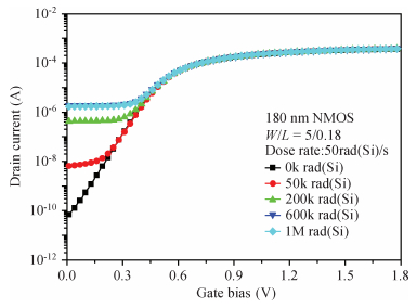
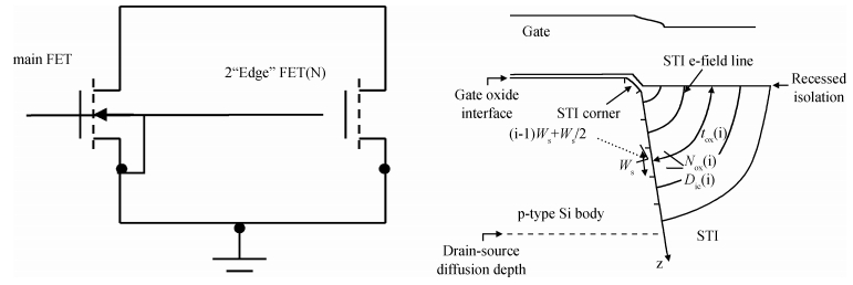
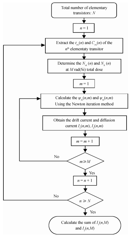
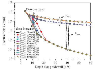
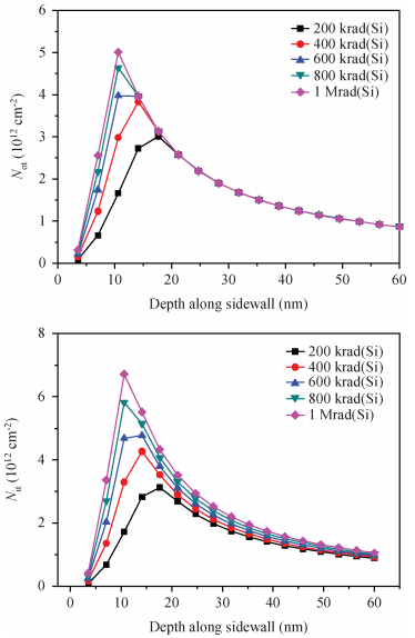
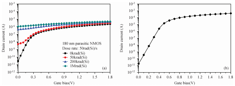
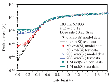
In this paper, total ionizing dose effect of NMOS transistors in advanced CMOS technology are examined. The radiation tests are performed at 60Co sources at the dose rate of 50 rad (Si)/s. The investigation's results show that the radiation-induced charge buildup in the gate oxide can be ignored, and the field oxide isolation structure is the main total dose problem. The total ionizing dose (TID) radiation effects of field oxide parasitic transistors are studied in detail. An analytical model of radiation defect charge induced by TID damage in field oxide is established. The I-V characteristics of the NMOS parasitic transistors at different doses are modeled by using a surface potential method. The modeling method is verified by the experimental I-V characteristics of 180 nm commercial NMOS device induced by TID radiation at different doses. The model results are in good agreement with the radiation experimental results, which shows the analytical model can accurately predict the radiation response characteristics of advanced bulk CMOS technology device.

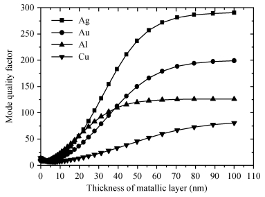
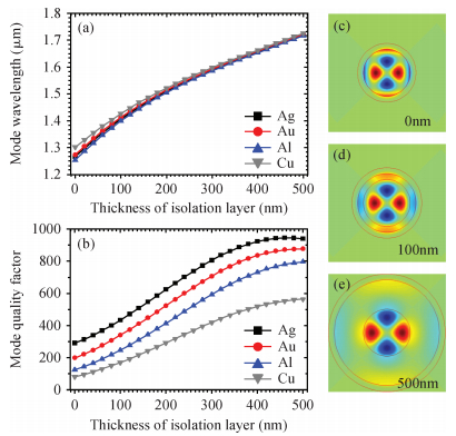
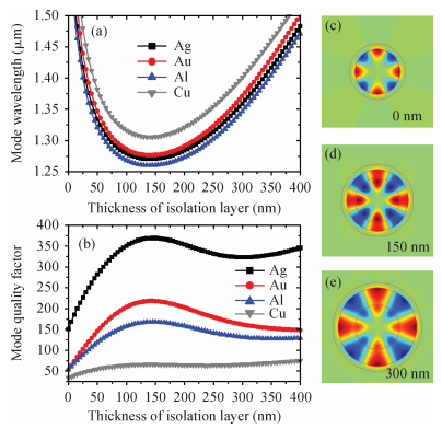
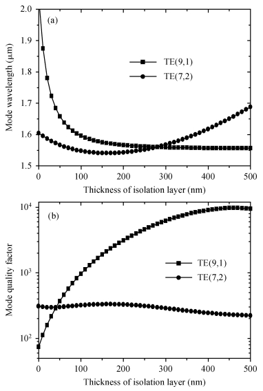
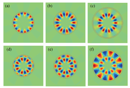
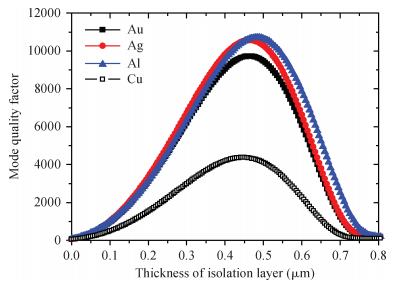
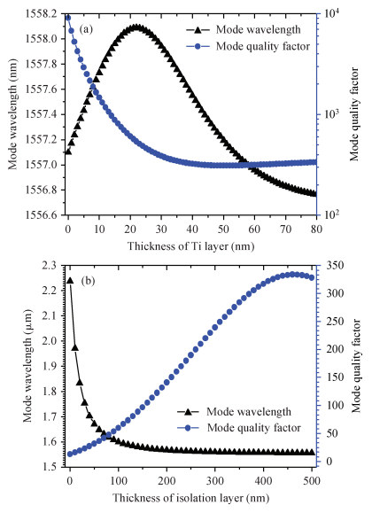
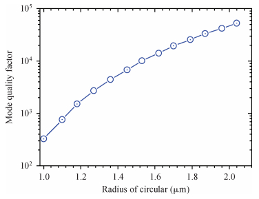
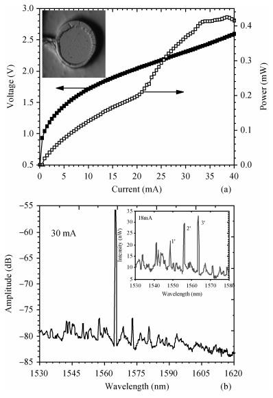
Mode characteristics of metallically confined microcircular resonators are theoretically studied by solving eigenvalue equations for two-dimensional multilayer structures. The influences of conventional metals including Au, Ag, Cu, Al, and Ti, on the mode wavelengths and Q factors of whispering gallery modes (WGMs) are analyzed and compared. The results show silver has the best optical confinement among these metals, and aluminum presents similar behavior to Au. However, Ti, which is usually applied to enhance the adhesion of p-electrode to semiconductors, results in a great dissipation for confined modes. Furthermore, circular microlasers with Al as both p-electrode and optical confinement medium are fabricated, and continuous-wave operations are realized at room temperature for the microlasers with a radius of 15 μm.

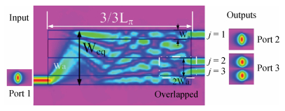
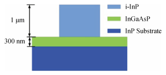
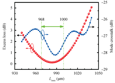
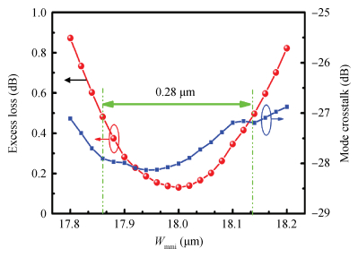
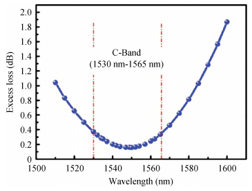
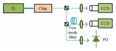
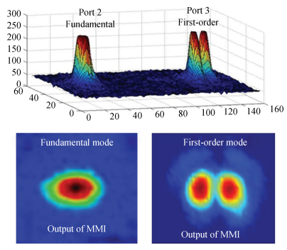
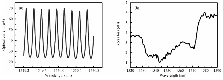
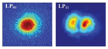
The design, fabrication and characterization of a fundamental/first-order mode converter based on multimode interference coupler on InP substrate were reported. Detailed optimization of the device parameters were investigated using 3D beam propagation method. In the experiments, the fabricated mode converter realized mode conversion from the fundamental mode to the first-order mode in the wavelength range of 1530-1565 nm with excess loss less than 3 dB. Moreover, LP01 and LP11 fiber modes were successfully excited from a few-mode fiber by using the device. This InP-based mode converter can be a possible candidate for integrated transceivers for future mode-division multiplexing system.


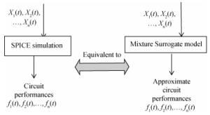
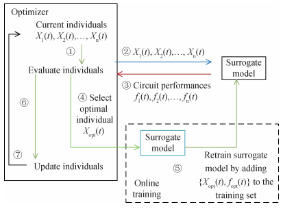
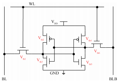
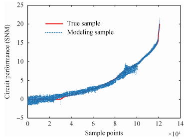
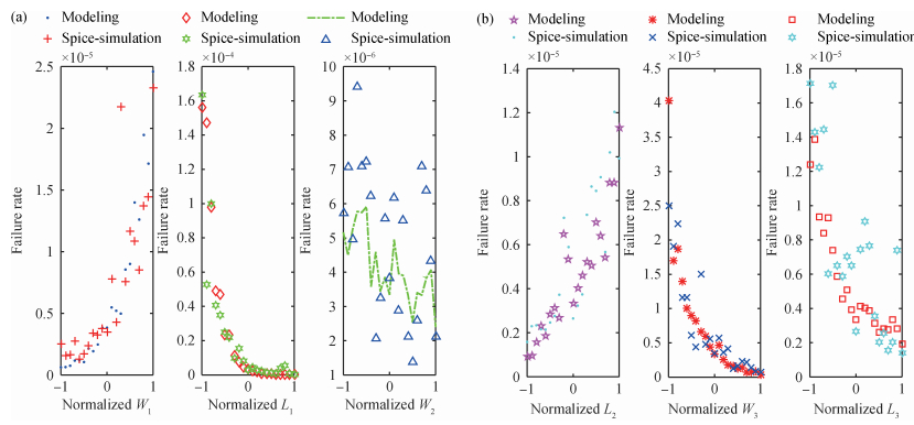
Largely repeated cells such as SRAM cells usually require extremely low failure-rate to ensure a moderate chi yield. Though fast Monte Carlo methods such as importance sampling and its variants can be used for yield estimation, they are still very expensive if one needs to perform optimization based on such estimations. Typically the process of yield calculation requires a lot of SPICE simulation. The circuit SPICE simulation analysis accounted for the largest proportion of time in the process yield calculation. In the paper, a new method is proposed to address this issue. The key idea is to establish an efficient mixture surrogate model. The surrogate model is based on the design variables and process variables. This model construction method is based on the SPICE simulation to get a certain amount of sample points, these points are trained for mixture surrogate model by the lasso algorithm. Experimental results show that the proposed model is able to calculate accurate yield successfully and it brings significant speed ups to the calculation of failure rate. Based on the model, we made a further accelerated algorithm to further enhance the speed of the yield calculation. It is suitable for high-dimensional process variables and multi-performance applications.

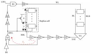
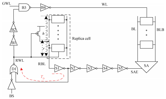
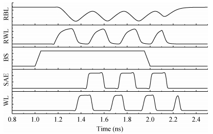
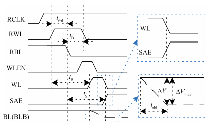
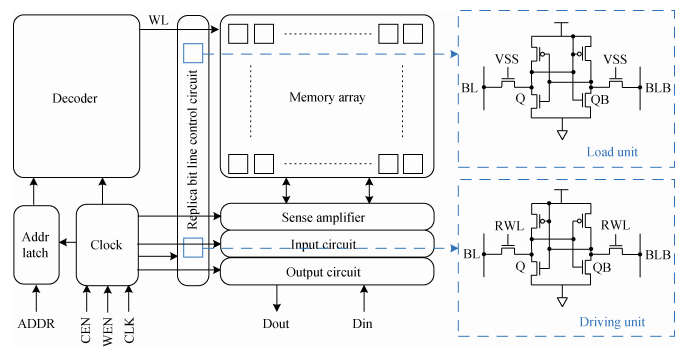
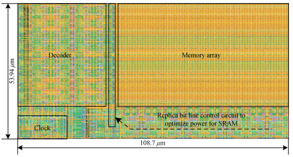
A design of a replica bit line control circuit to optimize power for SRAM is proposed. The proposed design overcomes the limitations of the traditional replica bit line control circuit, which cannot shut off the word line in time. In the novel design, the delay of word line enable and disable paths are balanced. Thus, the word line can be opened and shut off in time. Moreover, the chip select signal is decomposed, which prevents feedback oscillations caused by the replica bit line and the replica word line. As a result, the switch power caused by unnecessary discharging of the bit line is reduced. A 2-kb SRAM is fully custom designed in an SMIC 65-nm CMOS process. The traditional replica bit line control circuit and the new replica bit line control circuit are used in the designed SRAM, and their performances are compared with each other. The experimental results show that at a supply voltage of 1.2 V, the switch power consumption of the memory array can be reduced by 53.7%.