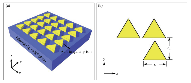
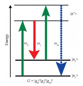
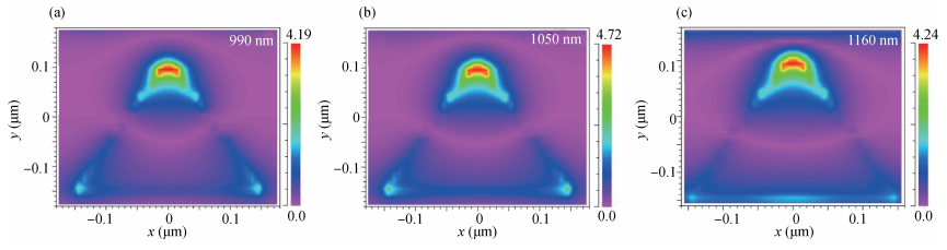
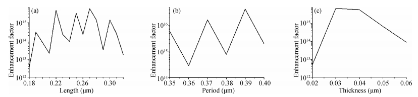
Coherent anti-Stokes Raman scattering spectroscopy(CARS) is a well-known detecting tool in biosensing and nonlinear spectroscopy. It can provide a non-invasive alternative without the need for exogenous labels, while the enhancement factor for surface plasmon resonances(SPR) are extensively used to increase the local field close to the oscillators and which can obtain high enhancement. In this work, we investigate the enhancement factor of our structure for surface-enhanced coherent anti-Stokes Raman scattering. The absorption spectrum of the structure has been studied, a wide range of absorption has been realized. The enhancement can be as high as 1016 over standard CARS. Our design is very useful for improving the enhancement factor of surface-enhanced coherent anti-Stokes Raman scattering.


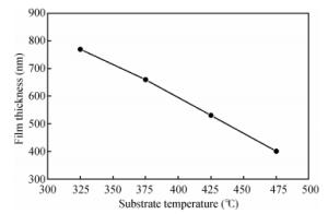
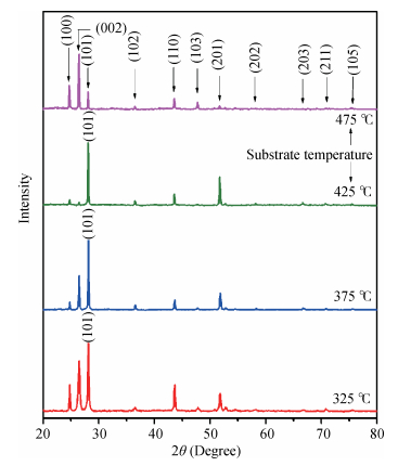
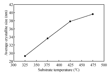
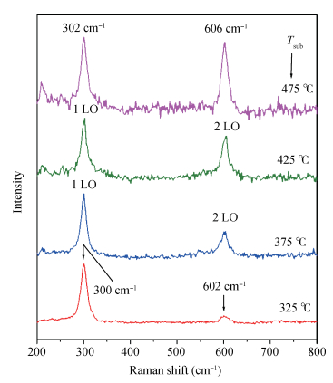
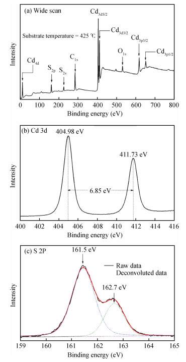
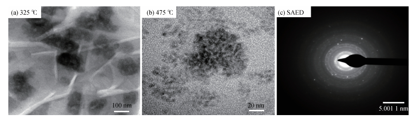
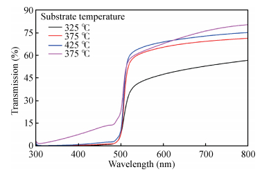
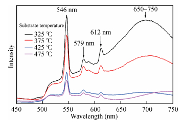
Thin films of CdS have been prepared by chemical spray pyrolysis by spraying precursor solution directly onto soda lime glass(SLG) substrates. Influence of substrate temperature on structural, optical, morphological and electrical properties have been investigated by using various techniques such as low angle X-ray diffraction(XRD), Raman spectroscopy, X-ray photoelectron spectroscopy(XPS), field emission scanning electron microscopy(FESEM), atomic force microscopy(AFM), transmission electron microscopy(TEM), UV-visible spectroscopy photoluminescence(PL) spectroscopy etc. Formation of CdS has been confirmed by low angle XRD, Raman spectroscopy and XPS analysis. XRD pattern showed that CdS films are polycrystalline, have hexagonal structure and prefer orientation of crystallites shifts from(101) to(002) with increase in substrate temperature. Raman spectroscopy revealed that exciton-phonon coupling depends on substrate temperature and hence on crystallite size. Optical band gap increased from 2.43 to 2.99 eV when substrate temperature increased from 325 to 475℃. Transmittance of the film also showed an increasing trend from ~52% to ~80% with increase in substrate temperature. Such high band gap and transmittance values of CdS films prepared at 475℃ make it a useful window material in CdS/CdTe and CdS/Cu2S heterojunction solar cells.


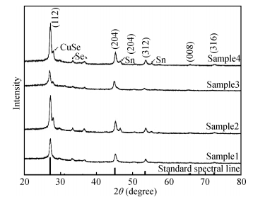
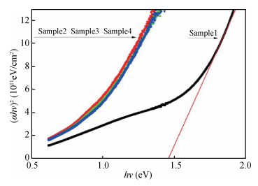
The CuZnSn(CZT) precursor thin films are grown by ion-beam sputtering Cu, Zn, Sn targets with different orders and then sputtering Se target to fabricate Cu2ZnSnSe4(CZTSe) absorber thin films on molybdenum substrates. They are annealed in the same vacuum chamber at 400℃. The characterization methods of CZTSe thin films include X-ray diffraction(XRD), energy dispersive spectroscopy(EDS), scanning electron microscopy(SEM), and X-ray photoelectron spectra(XPS) in order to study the crystallographic properties, composition, surface morphology, electrical properties and so on. The results display that the CZTSe thin films got the strongest diffraction peak intensity and were with good crystalline quality and its morphology appeared smooth and compact with a sequence of Cu/Zn/Sn/Se, which reveals that the expected states for CZTSe are Cu1+, Zn2+, Sn4+, Se2+. With the good crystalline quality and close to ideal stoichiometric ratio the resistivity of the CZTSe film with the sequence of Cu/Zn/Sn/Se is lower, whose optical band gap is about 1.50 eV.


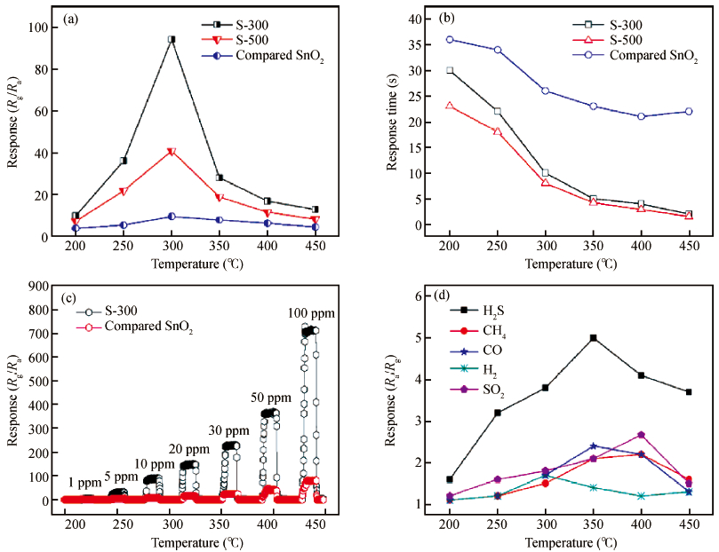
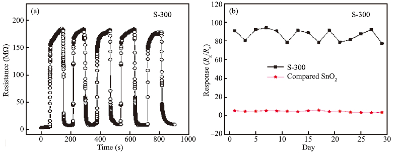
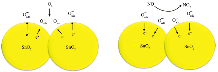
Mesoporous tin oxide(SnO2/with a high surface area of 147.5 m2/g has been successfully synthesized via self-assembly process, combining the driven forces of water-evaporation and molecular interactions. Scanning electron microscope, X-ray diffraction, transmission electron micrograph, Fourier transform infrared and BrunauerEmmett-Teller were employed to analyze the morphology and crystal structure of the as-synthesized mesoporous materials. As a gas sensor, mesoporous SnO2 shows impressive performances towards NOx gas with high selectivity and stability as well as ultra high sensitivity about 94.3 to 10 ppm NOx gas at 300℃. The best response time of the sample S-500 is about 3.4s to 10 ppm NOx at 450℃.


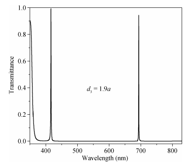
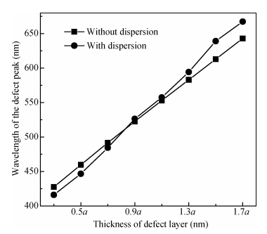
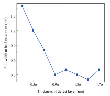
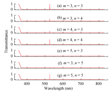
By inserting an air cavity into a one-dimensional photonic crystal of LiF/GaSb, a tunable filter covering the whole visible range is proposed. Following consideration of the dispersion of the materials, through modulating the thickness of the air cavity, we demonstrate that a single resonant peak can shift from 416.1 to 667.3 nm in the band gap at normal incidence by means of the transfer matrix method. The research also shows that the transmittance of the channel can be maximized when the number of periodic LiF/GaSb layers on one side of the air defect layer is equal to that of the other side. When adding a period to both sides respectively, the full width at half maximum of the defect mode is reduced by one order of magnitude. This structure will provide a promising approach to fabricate practical tunable filters in the visible region with ultra-wide tuning range.


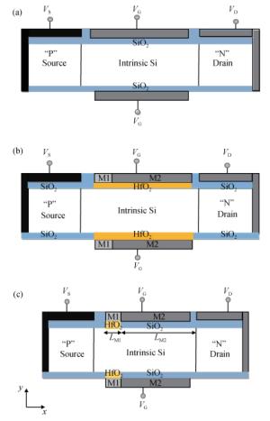
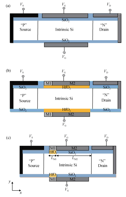
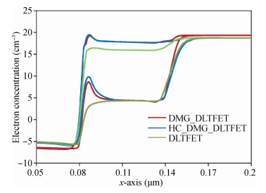
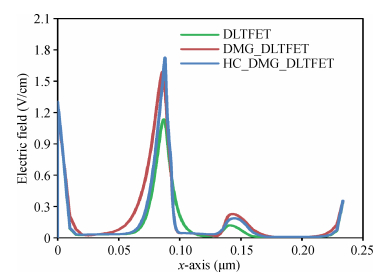
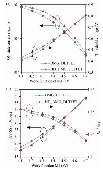
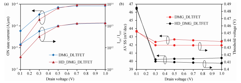
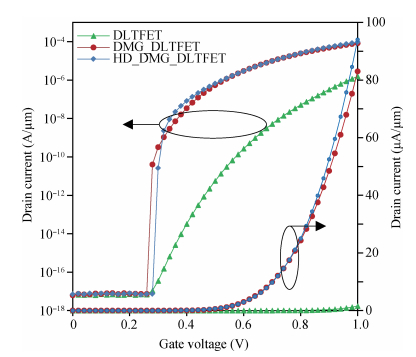
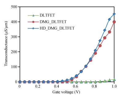
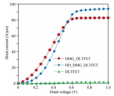
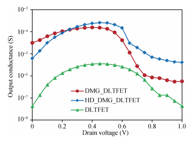
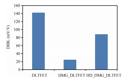
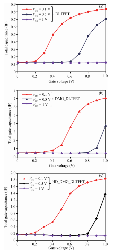
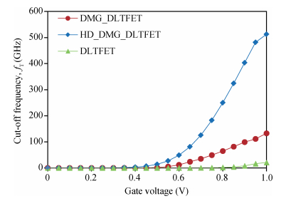
In this paper, charge-plasma-based tunnel FET is proposed by employing dual material gate with hetero gate dielectric technique and it is named hetero-dielectric dual material gate doping-less TFET(HD_DMG_DLTFET). It is compared with conventional doping-less TFET(DLTFET) and dual material gate doping-less TFET(DMG_DLTFET) on the basis of analog and RF performance. The HD_DMG_DLTFET provides better ON state current(ION=94 μA/μm), ION/IOFF(≈ 1:36×1013), point(≈ 3 mV/dec) and average subthreshold slope(AV-SS=40.40 mV/dec). The proposed device offers low total gate capacitance(Cgg)along with higher drive current. However, with a better transconductance(gm) and cut-off frequency(fT), the HD_DMG_DLTFET can be a good candidate for RF circuitry. The early voltage(VEA) and output conductance(gd) are also moderate for the proposed device with comparison to other devices and therefore can be a candidate for analog devices. From all these simulation results and their study, it is observed that HD_DMG_DLTFET has improved analog/RF performance compared to DLTFET and DMG_DLTFET.


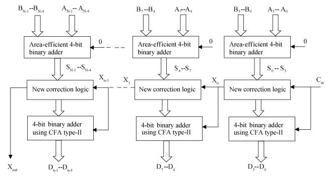
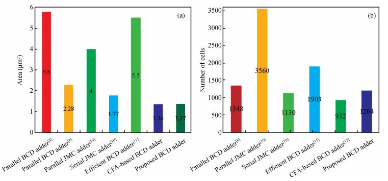
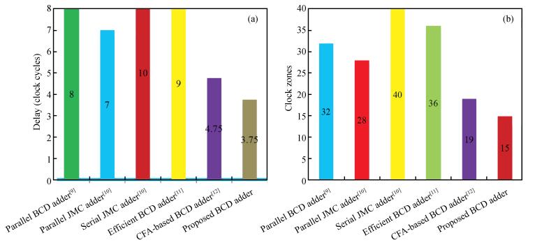
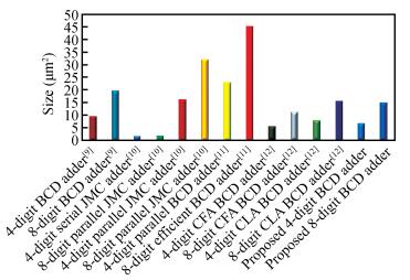
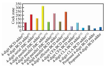
The advent of development of high-performance, low-power digital circuits is achieved by a suitable emerging nanodevice called quantum-dot cellular automata (QCA). Even though many efficient arithmetic circuits were designed using QCA, there is still a challenge to implement high-speed circuits in an optimized manner. Among these circuits, one of the essential structures is a parallel multi-digit decimal adder unit with significant speed which is very attractive for future environments. To achieve high speed, a new correction logic formulation method is proposed for single and multi-digit BCD adder. The proposed enhanced single-digit BCD adder (ESDBA) is 26% faster than the carry flow adder (CFA)-based BCD adder. The multi-digit operations are also performed using the proposed ESDBA, which is cascaded innovatively. The enhanced multi-digit BCD adder (EMDBA) performs two 4-digit and two 8-digit BCD addition 50% faster than the CFA-based BCD adder with the nominal overhead of the area. The EMDBA performs two 4-digit BCD addition 24% faster with 23% decrease in the area, similarly for 8-digit operation the EMDBA achieves 36% increase in speed with 21% less area compared to the existing carry look ahead (CLA)-based BCD adder design. The proposed multi-digit adder produces significantly less delay of (N-1)+3.5 clock cycles compared to the N*One digit BCD adder delay required by the conventional BCD adder method. It is observed that as per our knowledge this is the first innovative proposal for multi-digit BCD addition using QCA.


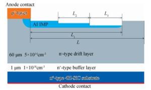
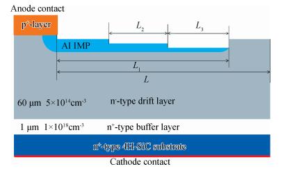
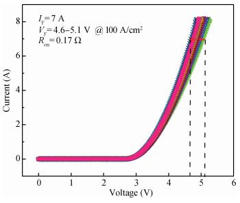
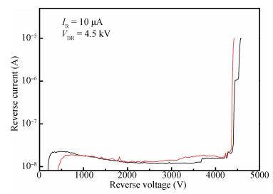
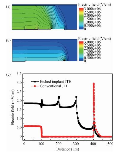
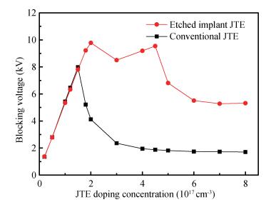
This paper presents the design and fabrication of an etched implant junction termination extension (JTE) for high-voltage 4H-SiC PiN diodes. Unlike the conventional JTE structure, the proposed structure utilizes multiple etching steps to achieve the optimum JTE concentration range. The simulation results show that the etched implant JTE method can improve the blocking voltage of SiC PiN diodes and also provides broad process latitude for parameter variations, such as implantation dose and activation annealing condition. The fabricated SiC PiN diodes with the etched implant JTE exhibit a highest blocking voltage of 4.5 kV and the forward on-state voltage of 4.6 V at room temperature. These results are of interest for understanding the etched implant method in the fabrication of high-voltage power devices.

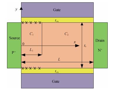
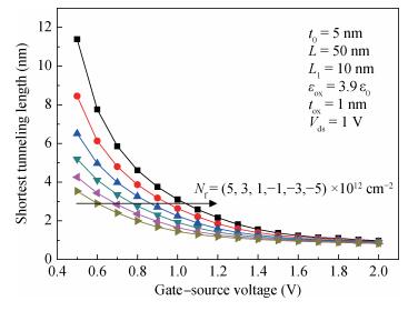
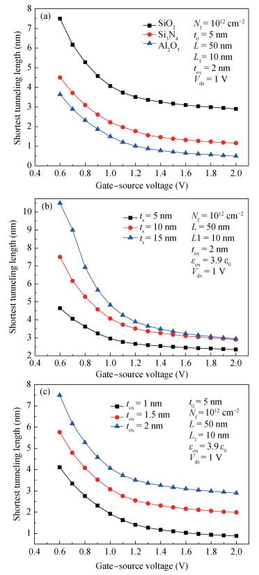
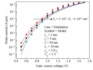
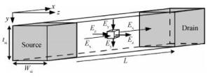
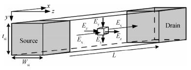
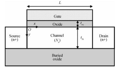
A two-dimensional analytical model of double-gate (DG) tunneling field-effect transistors (TFETs) with interface trapped charges is proposed in this paper. The influence of the channel mobile charges on the potential profile is also taken into account in order to improve the accuracy of the models. On the basis of potential profile, the electric field is derived and the expression for the drain current is obtained by integrating the BTBT generation rate. The model can be used to study the impact of interface trapped charges on the surface potential, the shortest tunneling length, the drain current and the threshold voltage for varying interface trapped charge densities, length of damaged region as well as the structural parameters of the DG TFET and can also be utilized to design the charge trapped memory devices based on TFET. The biggest advantage of this model is that it is more accurate, and in its expression there are no fitting parameters with small calculating amount. Very good agreements for both the potential, drain current and threshold voltage are observed between the model calculations and the simulated results.


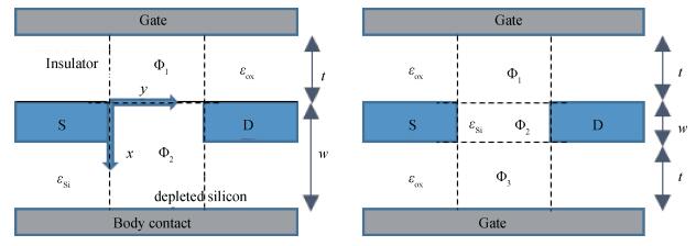
Subthreshold conduction is governed by the potential distribution. We focus on full two-dimensional (2D) analytical modeling in order to evaluate the 2D potential profile within the active area of FinFET structure. Surfaces and interfaces, which are key nanowire elements, are carefully studied. Different structures have different boundary conditions, and therefore different effects on the potential distributions. A range of models in FinFET are reviewed in this paper. Parabolic approximation and evanescent mode are two different basic math methods to simplify the Poisson's equation. Both superposition method and parabolic approximation are widely used in heavily doped devices. It is helpful to learn performances of MOSFETs with different structures. These two methods achieved improvement to face different structures from heavily doped devices or lightly doped devices to junctionless transistors.


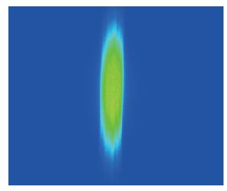
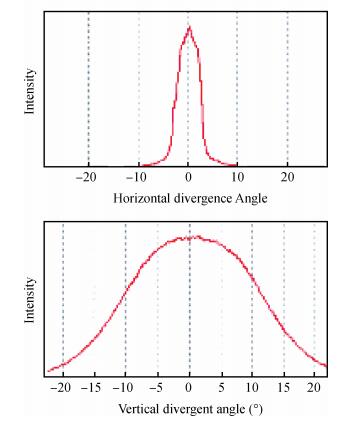
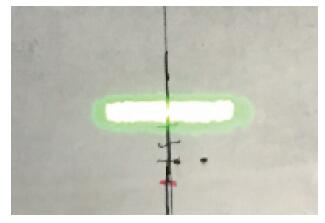
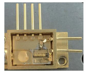
Based on the high-speed development of the fiber laser in recent years, the development of researching 915 nm semiconductor laser as main pumping sources of the fiber laser is at a high speed. Because the beam quality of the laser diode is very poor, the 915 nm laser diode is generally based on optical fiber coupling module to output the laser. Using the beam-shaping and fiber-coupling technology to improve the quality of output beam light, we present a kind of high-power and high-brightness semiconductor laser module, which can output 13.22 W through the optical fiber. Based on 915 nm GaAs semiconductor laser diode which has output power of 13.91 W, we describe a thoroughly detailed procedure for reshaping the beam output from the semiconductor laser diode and coupling the beam into the optical fiber of which the core diameter is 105 μm and the numerical aperture is 0.18. We get 13.22 W from the output fiber of the module at 14.5 A, the coupling efficiency of the whole module is 95.03% and the brightness is 1.5 MW/cm2-str. The output power of the single chip semiconductor laser module achieves the advanced level in the domestic use.


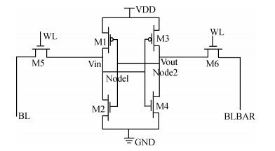
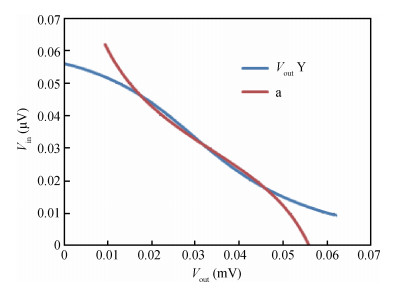
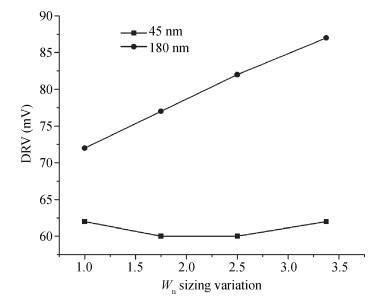
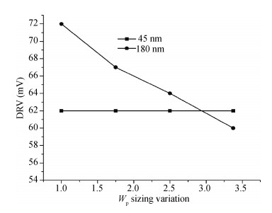
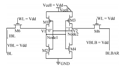
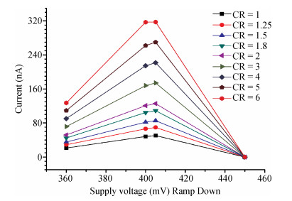
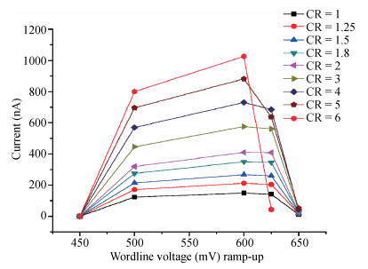
The present paper analyzes the hold and read stability with temperature and aspect ratio variations. To reduce the power dissipation, one of the effective techniques is the supply voltage reduction. At this reduced supply voltage the data must be stable. So, the minimum voltage should be discovered which can also retain the data. This voltage is the data retention voltage (DRV). The DRV for 6T SRAM cell is estimated and analyzed in this paper. The sensitivity analysis is performed for the DRV variation with the variation in the temperature and aspect ratio of the pull up and pull down transistors. Cadence Virtuoso is used for DRV analysis using 45 nm GPDK technology files. After this, the read stability analysis of 6T SRAM cell in terms of SRRV (supply read retention voltage) and WRRV (wordline read retention voltage) is carried out. Read stability in terms of RSNM can be discovered by accessing the internal storage nodes. But in the case of dense SRAM arrays instead of using internal storage nodes, the stability can be discovered by using direct bit line measurements with the help of SRRV and WRRV. SRRV is used to find the minimum supply voltage for which data can be retained during a read operation. Similarly, WRRV is used to find the boosted value of wordline voltage, for which data can be retained during read operation. The SRRV and WRRV values are then analyzed for different Cell Ratios. The results of SRRV and WRRV are then compared with the reported data for the validation of the accuracy of the results.


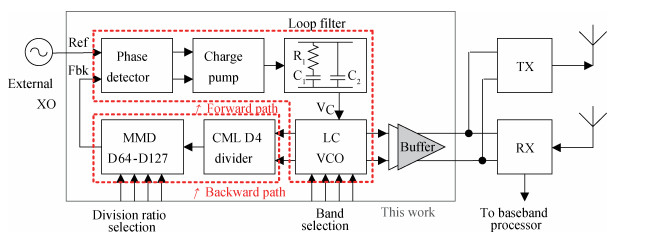
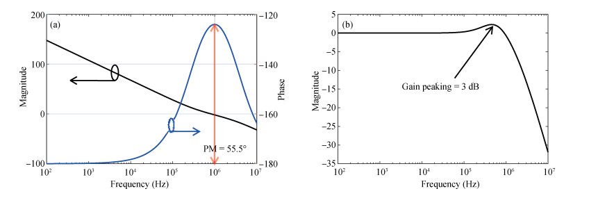
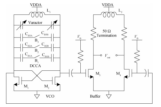
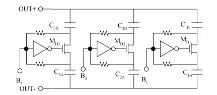
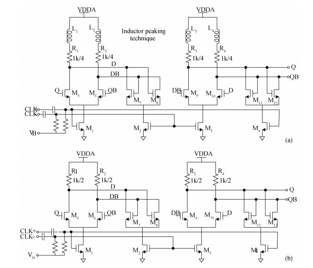
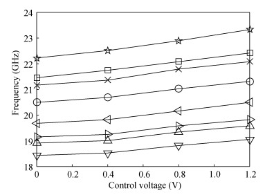
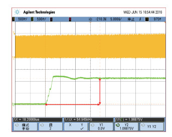
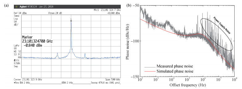
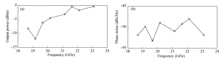
A monolithic K-band phase-locked loop (PLL) for microwave radar application is proposed and implemented in this paper. By eliminating the tail transistor and using optimized high-Q LC-tank, the proposed voltage-controlled oscillator (VCO) achieves a tuning range of 18.4 to 23.3 GHz and reduced phase noise. Two cascaded current-mode logic (CML) divide-by-two frequency prescalers are implemented to bridge the frequency gap, in which inductor peaking technique is used in the first stage to further boost allowable input frequency. Six-stage TSPC divider chain is used to provide programmable division ratio from 64 to 127, and a second-order passive loop filter with 825 kHz bandwidth is also integrated on-chip to minimize required external components. The proposed PLL needs only approximately 18.2 μs settling time, and achieves a wide tuning range from 18.4 to 23.3 GHz, with a typical output power of -0.84 dBm and phase noise of 91:92 dBc/Hz@1 MHz. The chip is implemented in TSMC 65 nm CMOS process, and occupies an area of 0.56 mm2 without pads under a 1.2 V single voltage supply.


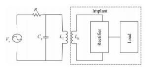
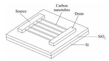
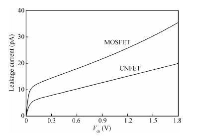
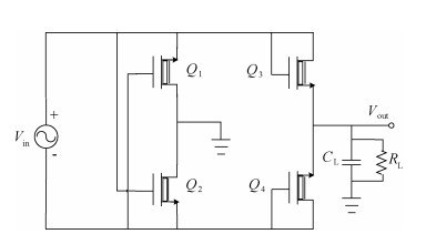
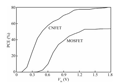
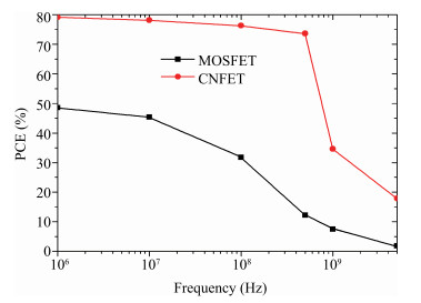
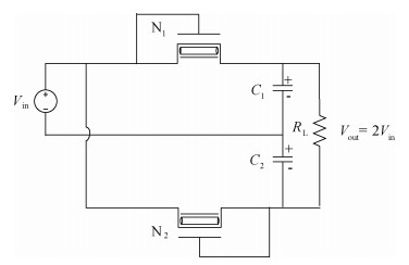
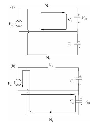
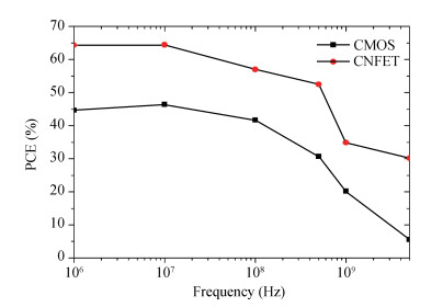
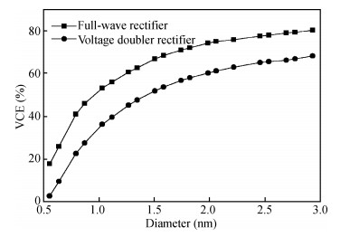
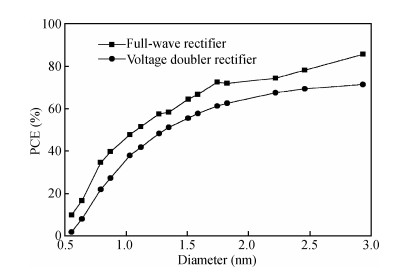
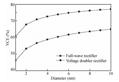
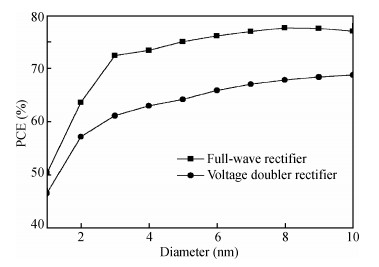
Carbon nanotube field effect transistor (CNFET) shows lower threshold voltage and smaller leakage current in comparison to its CMOS counterpart. In this paper, two kinds of CNFET-based rectifiers, full-wave rectifiers and voltage doubler rectifiers are presented for biomedical implantable applications. Based on the standard 32 nm CNFET model, the electrical performance of CNFET rectifiers is analyzed and compared. Simulation results show the voltage conversion efficiency (VCE) and power conversion efficiency (PCE) achieve 70.82% and 72.49% for CNFET full-wave rectifiers and 56.60% and 61.17% for CNFET voltage double rectifiers at typical 1.0 V input voltage excitation, which are higher than that of CMOS design. Moreover, considering the controllable property of CNFET threshold voltage, the effect of various design parameters on the electrical performance is investigated. It is observed that the VCE and PCE of CNFET rectifier increase with increasing CNT diameter and number of tubes. The proposed results would provide some guidelines for design and optimization of CNFET-based rectifier circuits.


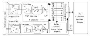
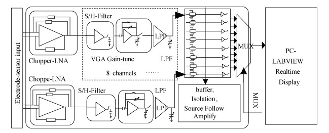
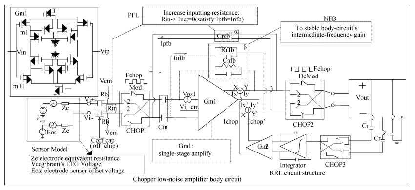
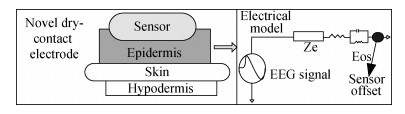
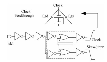
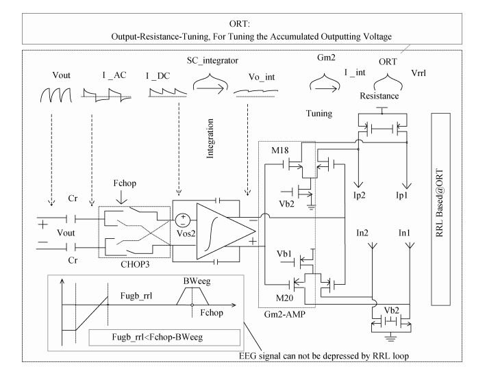
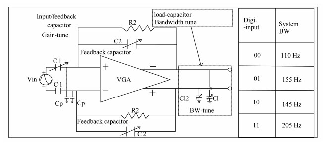
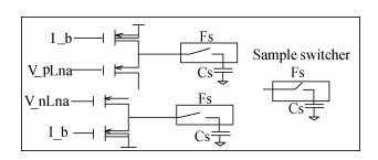
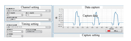
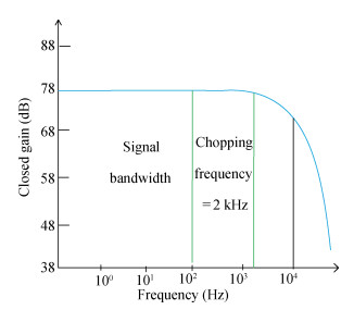
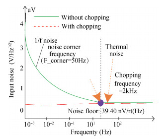
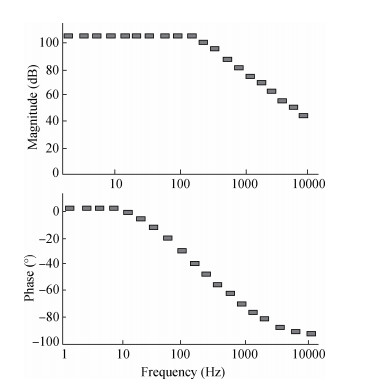
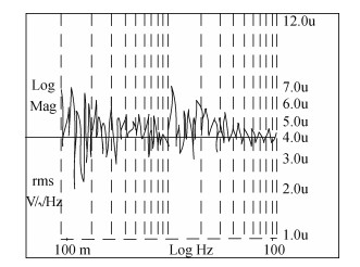
Facing the body's EEG (electroencephalograph, 0.5-100Hz, 5-100 μV) and ECG's (electrocardiogram, < 100Hz, 0.01-5mV) micro signal detection requirement, this paper develops a pervasive application micro signal detection ASIC chip with the chopping modulation/demodulation method. The chopper-stabilization circuit with the RRL (ripple reduction loop) circuit is to suppress the ripple voltage, which locates at the single-stage amplifier's outputting terminal. The single-stage chopping core's noise has been suppressed too, and it is beneficial for suppressing noises of post-circuit. The chopping core circuit uses the PFB (positive feedback loop) to increase the inputting resistance, and the NFB (negative feedback loop) to stabilize the 40 dB intermediate frequency gain. The cascaded switch-capacitor sample/hold circuit has been used for deleting spike noises caused by non-ideal MOS switches, and the VGA/BPF (voltage gain amplifier/band pass filter) circuit is used to tune the chopper system's gain/bandwidth digitally. Assisted with the designed novel dry-electrode, the real test result of the chopping amplifying circuit gives some critical parameters:8.1 μW/channel, 0.8 μVrms (@band-width=100 Hz), 4216-11220 times digitally tuning gain range, etc. The data capture system uses the NI CO's data capturing DAQmx interface, and the captured micro EEG/ECG's waves are real-time displayed with the PC-Labview. The proposed chopper system is a unified EEG/ECG signal's detection instrument and has a critical real application value.