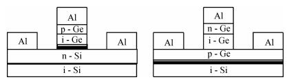
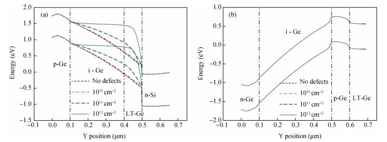
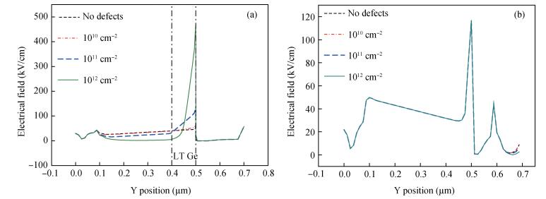
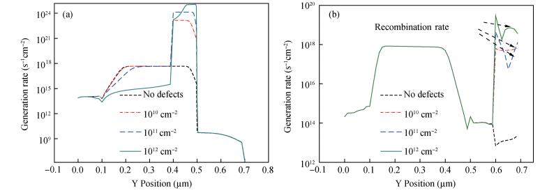
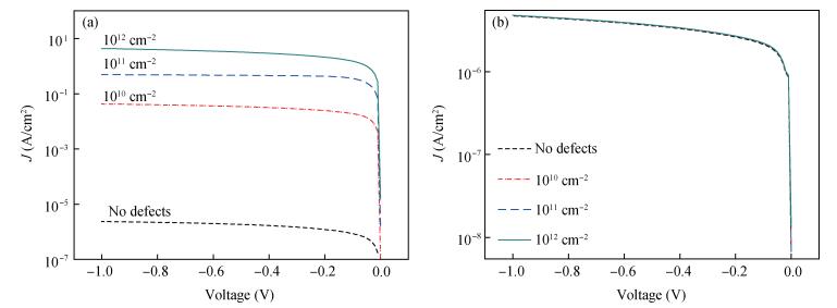
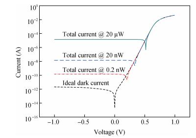
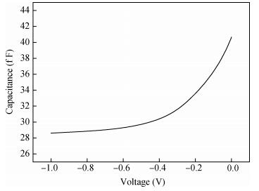
The influence of defects in low temperature Ge layer on electrical characteristics of p-Ge/i-Ge/n-Si and n-Ge/i-Ge/p-Ge photodiodes (PDs) was studied. Due to a two-step growth method, there are high defect densities in low-temperature buffer Ge layer. It is shown that the defects in low-temperature Ge layer change the band diagrams and the distribution of electric field, leading to the increase of the total dark current for p-Ge/i-Ge/n-Si PDs, whereas these defects have no influence on the dark current for n-Ge/i-Ge/p-Ge PDs. As a complement, a three-dimensional simulation of the total current under illumination was also performed.
Issue Browser
Volume 38, Issue 4,
Apr 2017
J. Semicond.
2017, 38(4): 042002 doi: 10.1088/1674-4926/38/4/042002
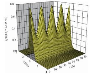
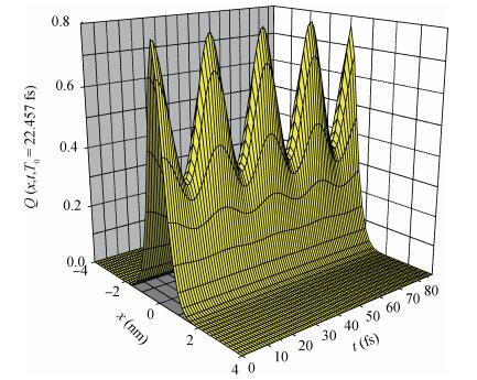
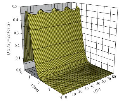
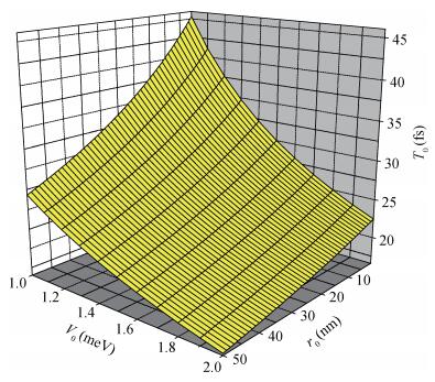
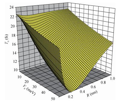
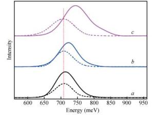
With the circumstance of the electron strongly coupled to LO-phonon and using the variational method of Pekar type (VMPT), we study the eigenenergies and the eigenfunctions (EE) of the ground and the first excited states (GFES) in a RbCl crystal asymmetric Gaussian potential quantum well (AGPQW). It concludes: (i) Two-energy-level of the AGPQW may be seen as a qubit. (ii) When the electron located in the superposition state of the two-energy-level system, the time evolution and the coordinate changes of the electron probability density oscillated periodically in the AGPQW with every certain period T0=22.475 fs. (iii) Due to the confinement that is a two dimensional x-y plane symmetric structure in the AGPQW and the asymmetrical Gaussian potential (AGP) in the AGPQW growth direction, the electron probability density presents only one peak configuration located in the coordinate of z>0, whereas it is zero in the range of z < 0. (iv) The oscillatory period is a decreasing function of the AGPQW height and the polaron radius. (v) The oscillating period is a decreasing one in the confinement potential R < 0.24 nm, whereas it is an increasing one in the confinement potential R>0.24 nm and it takes a minimum value in R=0.24 nm.

J. Semicond.
2017, 38(4): 042003 doi: 10.1088/1674-4926/38/4/042003

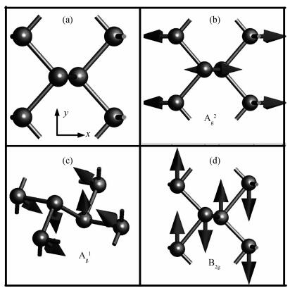
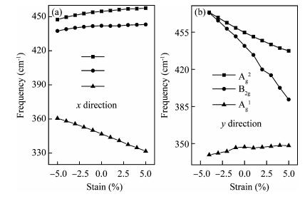
Phosphorene has a very high hole mobility and can be a tuned band structure, and has become an ideal material for electronic devices. For this new type of two-dimensional material, in the applied strain, black phosphorus (BP) can be changed into an indirect band gap and metallic materials from the direct band gap semiconductor material, which greatly affect its inherent physical characteristics. How to identify strained microstructure changes becomes an important problem. The calculated Raman spectra disclose that the Ag2 mode and B2g mode will split and the Raman spectra appear, while the Ag1 mode is shifted to low-frequency region. The deformation induced by strain will effectively change the Raman mode position and intensity, this can be used to identify phosphorus changes.


J. Semicond.
2017, 38(4): 042004 doi: 10.1088/1674-4926/38/4/042004

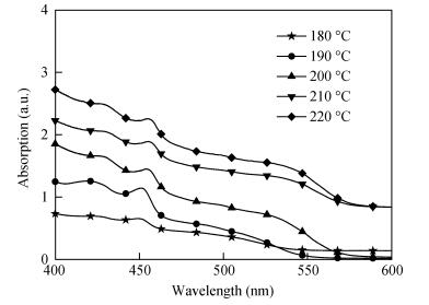
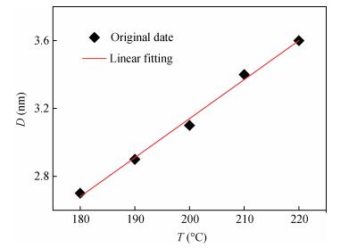
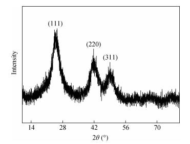
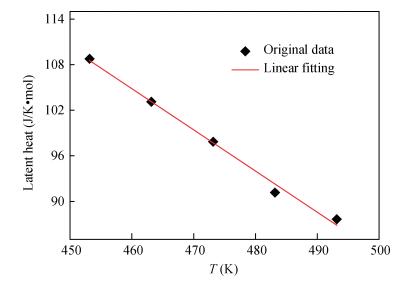
This work studied the effect of differential temperatures on the latent heat in the nucleation of CdSe quantum dots (QDs). The result showed that, by the formula of phase change, with increasing the reaction temperature, the latent heat in the nucleation of QDs reduced. CdSe QDs with the size-dispersion from 2.7 to 3.6 nm were synthesized via oleic acid-paraffin liquid system by controlling the reaction temperature from 180 to 220 ℃. Synthesized QDs were characterized by UV-vis absorption spectra and X-ray diffraction (XRD). The result of UV-vis absorption spectra showed that with increasing of reaction temperature, the first absorption peak was red-shifted and the size of QD increased. The result of XRD showed that the synthesized QDs were zinc-blende structure.
J. Semicond.
2017, 38(4): 043001 doi: 10.1088/1674-4926/38/4/043001
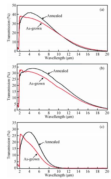
GaSb is the most suitable substrate in the epitaxial growth of mixed semiconductors of GaSb system. In this work, Te-doped GaSb bulk crystals with different doping concentration have been annealed at 550 ℃ for 100 h in ambient antimony. The annealed samples have been studied by Hall effect measurement, infrared (IR) optical transmission, Glow discharge mass spectroscopy (GDMS) and photoluminescence (PL) spectroscopy. After annealing, Te-doped GaSb samples exhibit a decrease of carrier concentration and increase of mobility, along with an improvement of below gap IR transmission. Native acceptor related electrical compensation analysis suggests a formation of donor defect with deeper energy level. The mechanism of the variation of the defect and its influence on the material properties are discussed.
J. Semicond.
2017, 38(4): 043002 doi: 10.1088/1674-4926/38/4/043002
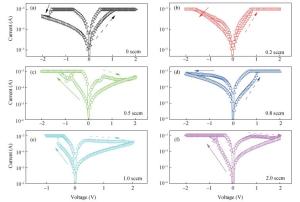
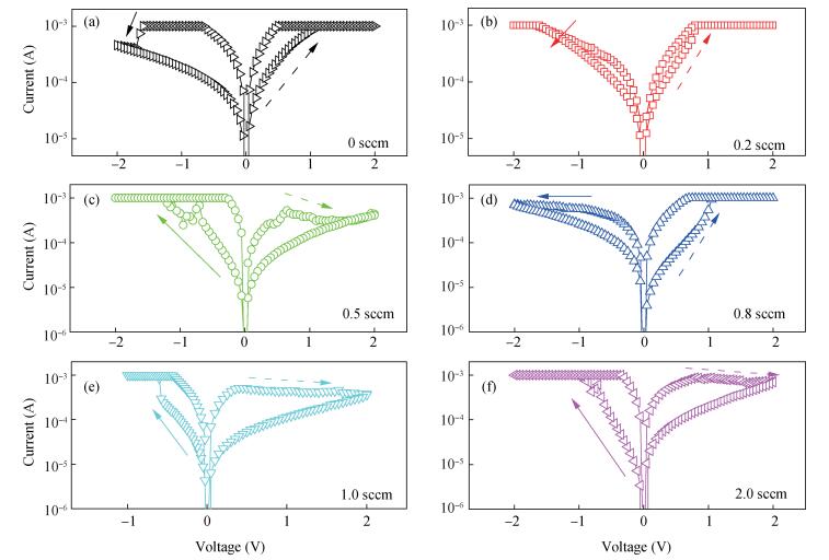
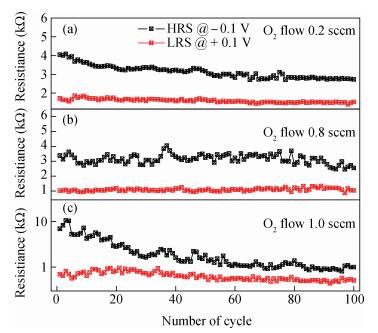
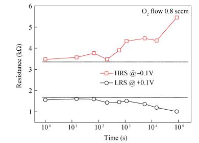
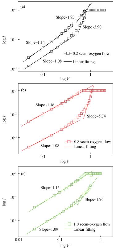
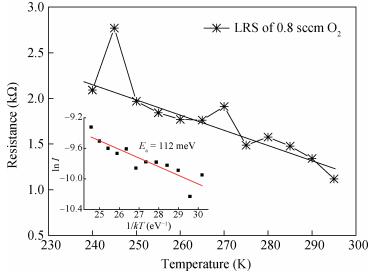
SiOxNy films with different oxygen concentrations were fabricated by reactive magnetron sputtering, and the resistive switching characteristics and conduction mechanism of Cu/SiOxNy/ITO devices were investigated. The Cu/SiOxNy/ITO device with SiOxNy deposited in 0.8-sccm O2 flow shows a reliable resistive switching behavior, including good endurance and retention properties. As the conductivity of SiOxNy increases with the increase of the oxygen content dynamical electron trapping and detrapping is suggested to be the conduction mechanism. The temperature dependent I-V measurement indicates that the carrier transport can be ascribed to the hopping conduction rather than the metallic conductive filament.
J. Semicond.
2017, 38(4): 044001 doi: 10.1088/1674-4926/38/4/044001
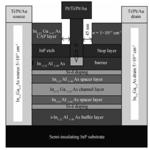
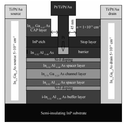
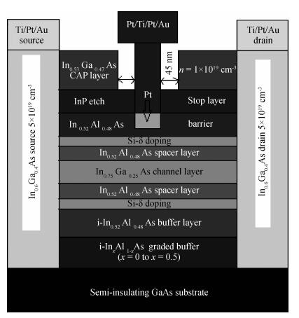
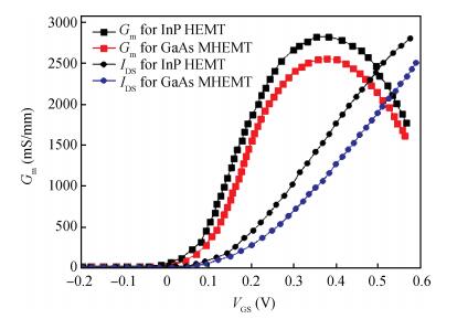
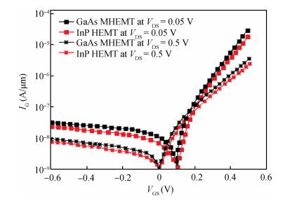
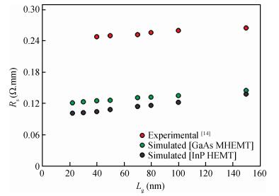
In this work, the performance of Lg=22 nm In0.75Ga0.25As channel-based high electron mobility transistor (HEMT) on InP substrate is compared with metamorphic high electron mobility transistor (MHEMT) on GaAs substrate. The devices features heavily doped In0.6Ga0.4As source/drain (S/D) regions, Si double δ-doping planar sheets on either side of the In0.75Ga0.25As channel layer to enhance the transconductance, and buried Pt metal gate technology for reducing short channel effects. The TCAD simulation results show that the InP HEMT performance is superior to GaAs MHEMT in terms of fT, fmax and transconductance (gm_max). The 22 nm InP HEMT shows an fT of 733 GHz and an fmax of 1340 GHz where as in GaAs MHEMT it is 644 GHz and 924 GHz, respectively. InGaAs channel-based HEMTs on InP/GaAs substrates are suitable for future sub-millimeter and millimeter wave applications.


J. Semicond.
2017, 38(4): 044002 doi: 10.1088/1674-4926/38/4/044002

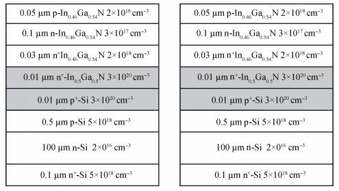
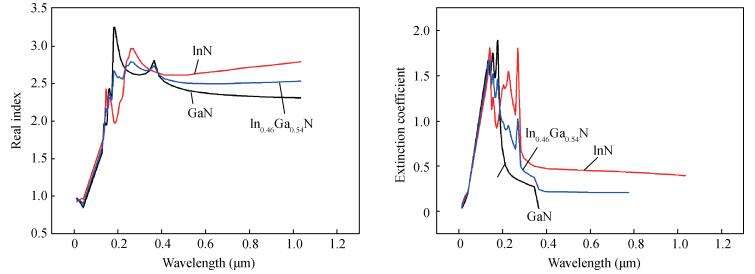
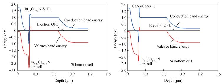
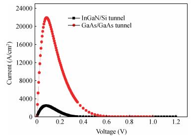
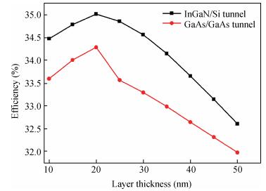
A comprehensive study of high efficiency In0.46Ga0.54N/Si tandem solar cell is presented. A tunnel junction (TJ) was needed to interconnect the top and bottom sub-cells. Two TJ designs, integrated within this tandem: GaAs (n+)/GaAs (p+) and In0.5Ga0.5N (n+)/Si (p+) were considered. Simulations of GaAs (n+)/GaAs (p+) and In0.5Ga0.5N (n+)/Si (p+) TJ I-V characteristics were studied for integration into the proposed tandem solar cell. A comparison of the simulated solar cell I-V characteristics under 1 sun AM1.5 spectrum was discussed in terms of short circuit current density (Jsc), open circuit voltage (VOC), fill factor (FF) and efficiency (η) for both tunnel junction designs. Using GaAs (n+)/GaAs (p+) tunnel junction, the obtained values of Jsc=21.74 mA/cm2, VOC=1.81 V, FF=0.87 and η=34.28%, whereas the solar cell with the In0.5Ga0.5N/Si tunnel junction reported values of Jsc=21.92 mA/cm2, VOC=1.81 V, FF=0.88 and η=35.01%. The results found that required thicknesses for GaAs (n+)/GaAs (p+) and In0.5Ga0.5N (n+)/Si (p+) tunnel junctions are around 20 nm, the total thickness of the top InGaN can be very small due to its high optical absorption coefficient and the use of a relatively thick bottom cell is necessary to increase the conversion efficiency.

J. Semicond.
2017, 38(4): 044003 doi: 10.1088/1674-4926/38/4/044003
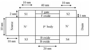
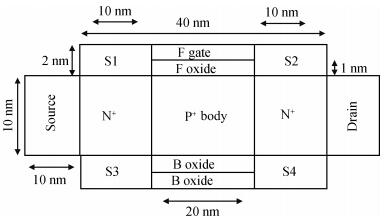
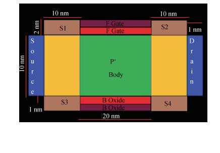
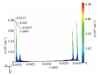
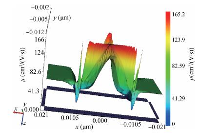
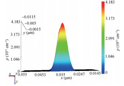
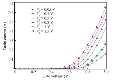
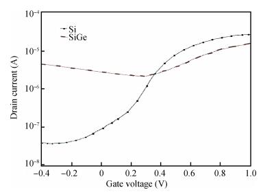
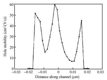
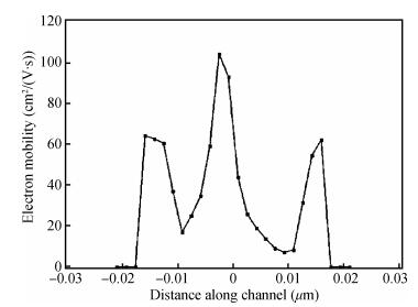
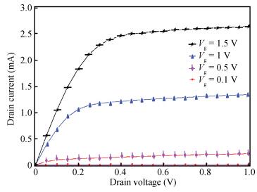
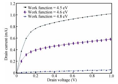
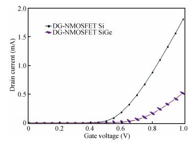
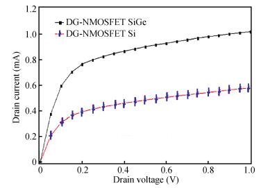
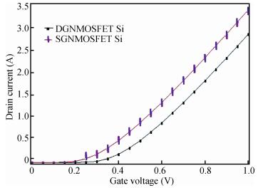
The major purpose of this paper is to find an alternative configuration that not only minimizes the limitations of single-gate (SG) MOSFETs but also provides the better replacement for future technology. In this paper, the electrical characteristics of SiGe double-gate N-MOSFET are demonstrated and compared with electrical characteristics of Si double-gate N-MOSFET. Furthermore, in this paper the electrical characteristics of Si double-gate N-MOSFET are demonstrated and compared with electrical characteristics of Si single-gate N-MOSFET. The simulations are carried out for the device at different operational voltages using Cogenda Visual TCAD tool. Moreover, we have designed its structure and studied both Id-Vg characteristics for different voltages namely 0.05, 0.1, 0.5, 0.8, 1 and 1.5 V and Id-Vd characteristics for different voltages namely 0.1, 0.5, 1 and 1.5 V at work functions 4.5, 4.6 and 4.8 eV for this structure. The performance parameters investigated in this paper are threshold voltage, DIBL, subthreshold slope, GIDL, volume inversion and MMCR.


J. Semicond.
2017, 38(4): 044004 doi: 10.1088/1674-4926/38/4/044004

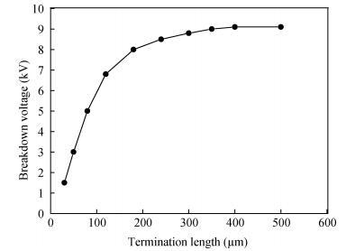
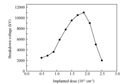
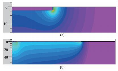
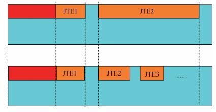
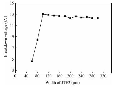
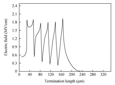
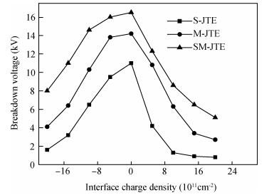
Numerical simulations on the optimization of junction termination extension (JTE) have been performed. Various termination techniques have been applied and simulated in this paper, such as single-zone JTE (S-JTE), multi-zone JTE (M-JTE), and space-modulated JTE (SM-JTE). A completely novel and efficient method is demonstrated in this paper to determine total length of SM-JTE, and it is verified through simulation results. The simulation results show that the SM-JTE could provide a protection efficiency (defined in Section 2) of 95.2%, which is much higher than that of M-JTE (82.4%) and S-JTE (64.7%). Based on the fabricated MOSFETs, the interface charge density is extracted and the approximate range of charge density has been determined. The influences of different interface charge densities have been investigated for the three termination techniques respectively. According to the previous reports, the JTE is quite sensitive to the implanted dose, so the blocking capability of each termination structure with different implanted doses is also simulated. The results show that when interface charge is considered, the SM-JTE always shows an enormous advantage over the other two junction termination structures, however the interface charge densities varied. The space-modulated JTE is also applicable to the power planar devices such as MOSFETs and IGBTs, which would provide a very promising lower fabrication cost.


J. Semicond.
2017, 38(4): 044005 doi: 10.1088/1674-4926/38/4/044005
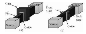
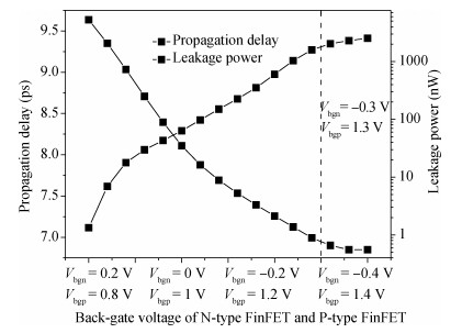
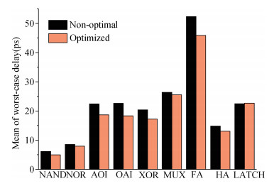
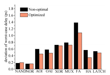
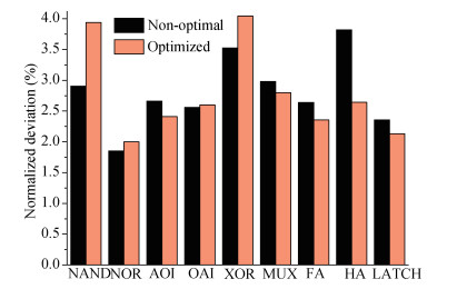
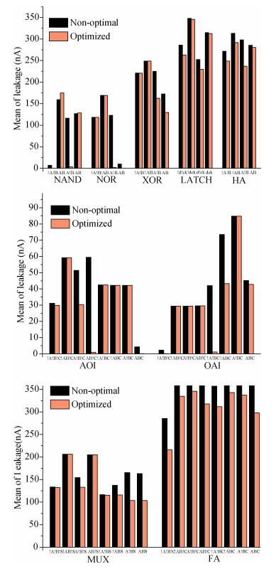
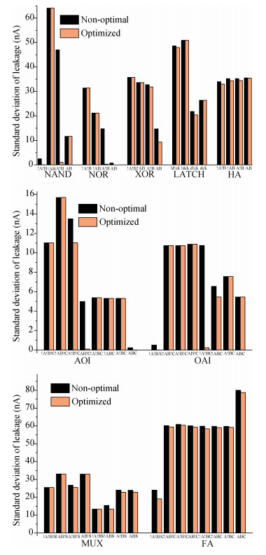
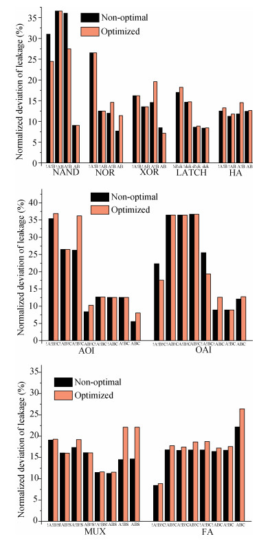
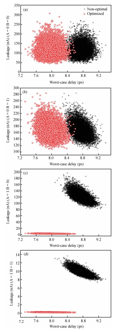
With shrinking transistor feature size, the fin-type field-effect transistor (FinFET) has become the most promising option in low-power circuit design due to its superior capability to suppress leakage. To support the VLSI digital system flow based on logic synthesis, we have designed an optimized high-performance low-power FinFET standard cell library based on employing the mixed FBB/RBB technique in the existing stacked structure of each cell. This paper presents the reliability evaluation of the optimized cells under process and operating environment variations based on Monte Carlo analysis. The variations are modelled with Gaussian distribution of the device parameters and 10000 sweeps are conducted in the simulation to obtain the statistical properties of the worst-case delay and input-dependent leakage for each cell. For comparison, a set of non-optimal cells that adopt the same topology without employing the mixed biasing technique is also generated. Experimental results show that the optimized cells achieve standard deviation reduction of 39.1% and 30.7% at most in worst-case delay and input-dependent leakage respectively while the normalized deviation shrinking in worst-case delay and input-dependent leakage can be up to 98.37% and 24.13%, respectively, which demonstrates that our optimized cells are less sensitive to variability and exhibit more reliability.


J. Semicond.
2017, 38(4): 044006 doi: 10.1088/1674-4926/38/4/044006

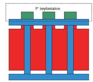
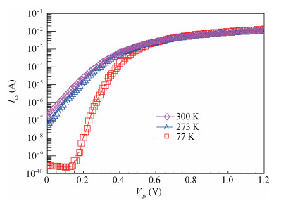
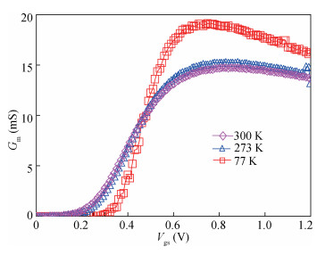
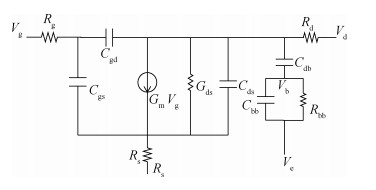
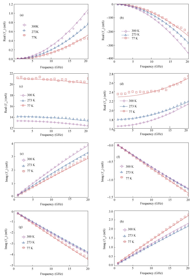
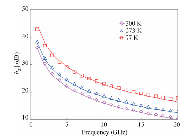
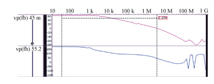
This paper investigated the temperature dependence of the cryogenic small-signal ac performances of multi-finger partially depleted (PD) silicon-on-insulator (SOI) metal oxide semiconductor field effect transistors (MOSFETs), with T-gate body contact (TB) structure. The measurement results show that the cut-off frequency increases from 78 GHz at 300 K to 120 GHz at 77 K and the maximum oscillation frequency increases from 54 GHz at 300 K to 80 GHz at 77 K, and these are mainly due to the effect of negative temperature dependence of threshold voltage and transconductance. By using a simple equivalent circuit model, the temperature-dependent small-signal parameters are discussed in detail. The understanding of cryogenic small-signal performance is beneficial to develop the PD SOI MOSFETs integrated circuits for ultra-low temperature applications.


J. Semicond.
2017, 38(4): 044007 doi: 10.1088/1674-4926/38/4/044007

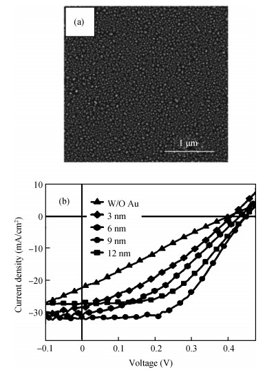
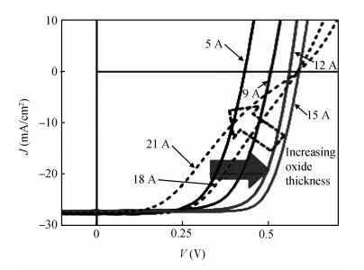
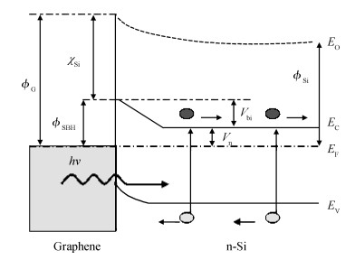
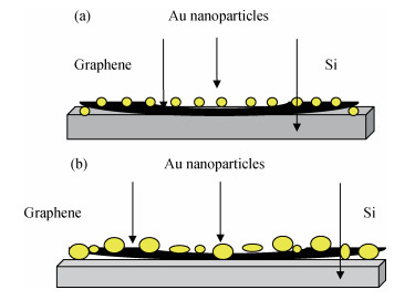
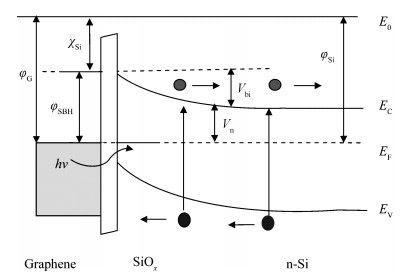
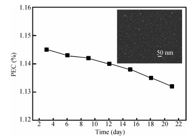
Here, we reply to comments by Valentic et al. on our paper published in Electrochimica Acta (2014, 130: 279). They commented that Au nanoparticles played the dominant role on the whole cell's performances in our improved graphene/Si solar cell. We argued that our devices are Au-doped graphene/n-Si Schottky barrier devices, not Au nanoparticles (film)/n-Si Schottky barrier devices. During the doping process, most of the Au nanopatricles covered the surfaces of the graphene. Schottky barriers between doped graphene and n-Si dominate the total cells properties. Through doping, by adjusting and tailoring the Fermi level of the graphene, the Fermi level of n-Si can be shifted down in the graphene/Si Schottky barrier cell. They also argued that the instability of our devices were related to variation in series resistance reduced at the beginning due to slightly lowered Fermi level and increased at the end by the self-compensation by deep in-diffusion of Au nanoparticles. But for our fabricated devices, we know that an oxide layer covered the Si surface, which makes it difficult for the Au ions to diffuse into the Si layer, due to the continuous growth of SiO2 layer on the Si surface which resulted in series resistance decreasing at first and increasing in the end.

J. Semicond.
2017, 38(4): 044008 doi: 10.1088/1674-4926/38/4/044008

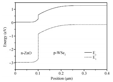
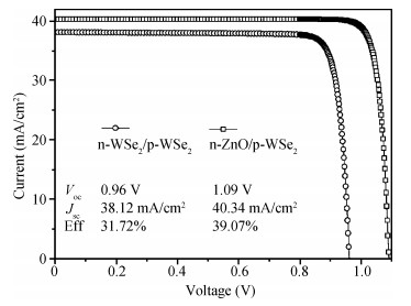
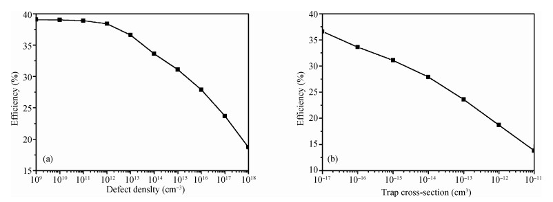
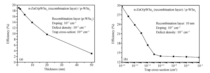
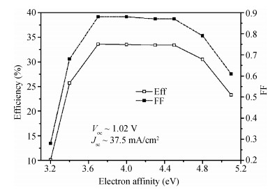
Taking into account defect density in WSe2, interface recombination between ZnO and WSe2, we presented a simulation study of ZnO/crystalline WSe2 heterojunction (HJ) solar cell using wxAMPS simulation software. The optimal conversion efficiency 39.07% for n-ZnO/p-c-WSe2 HJ solar cell can be realized without considering the impact of defects. High defect density (> 1.0 × 1011 cm-2) in c-WSe2 and large trap cross-section (> 1.0 × 10⁻¹⁰ cm2) have serious impact on solar cell efficiency. A thin p-WSe2 layer is intentionally inserted between ZnO layer and c-WSe2 to investigate the effect of the interface recombination. The interface properties are very crucial to the performance of ZnO/c-WSe2HJ solar cell. The affinity of ZnO value range between 3.7-4.5 eV gives the best conversion efficiency.
J. Semicond.
2017, 38(4): 044009 doi: 10.1088/1674-4926/38/4/044009
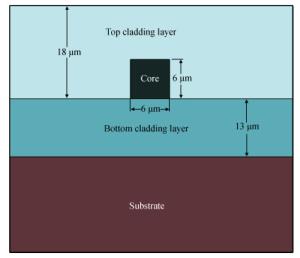
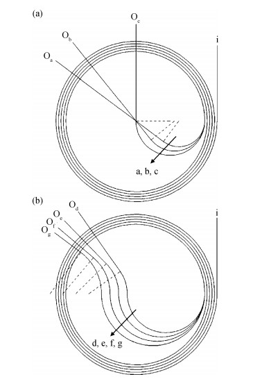
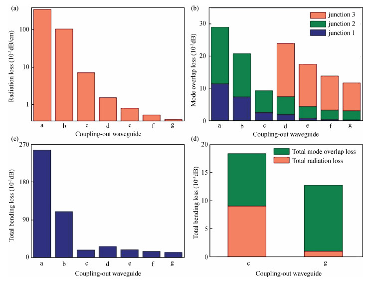
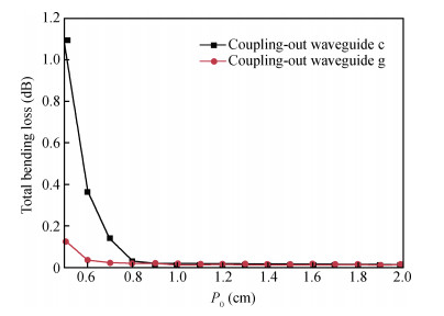
With the development of manufacturing technology, the propagation loss of the planar waveguide is getting lower and lower, and the shot-noise-limited sensitivity of an IIOG will be greatly improved. When the propagation loss is getting lower, improper coupling-out waveguide in the waveguide coil may lead to non-ignorable bending loss and crosstalk because of the small radius of curvature and X-junction. In this paper, different coupling-out waveguides have been designed. After calculation and optimization by the beam propagation method, we found the proper coupling-out waveguide having relatively low propagation loss, which can improve the sensitivity of the IIOG.


J. Semicond.
2017, 38(4): 044010 doi: 10.1088/1674-4926/38/4/044010

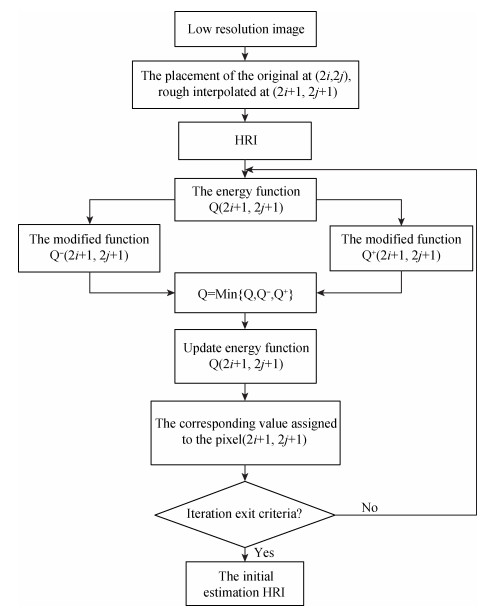
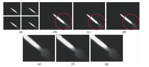
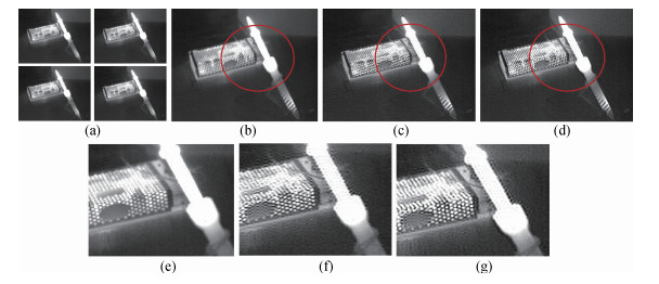
Aiming at the disadvantages of the traditional projection onto convex sets of blurry edges and lack of image details, this paper proposes an improved projection onto convex sets (POCS) method to enhance the quality of image super-resolution reconstruction (SRR). In traditional POCS method, bilinear interpolation easily blurs the image. In order to improve the initial estimation of high-resolution image (HRI) during reconstruction of POCS algorithm, the initial estimation of HRI is obtained through iterative curvature-based interpolation (ICBI) instead of bilinear interpolation. Compared with the traditional POCS algorithm, the experimental results in subjective evaluation and objective evaluation demonstrate the effectiveness of the proposed method. The visual effect is improved significantly and image detail information is preserved better.
J. Semicond.
2017, 38(4): 045001 doi: 10.1088/1674-4926/38/4/045001

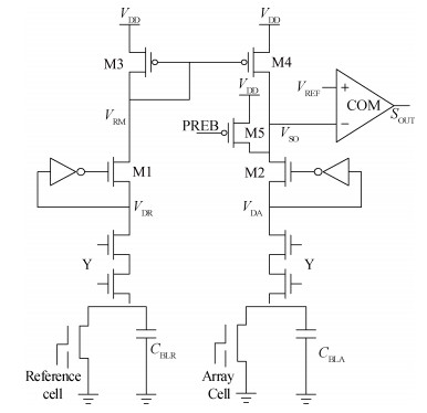
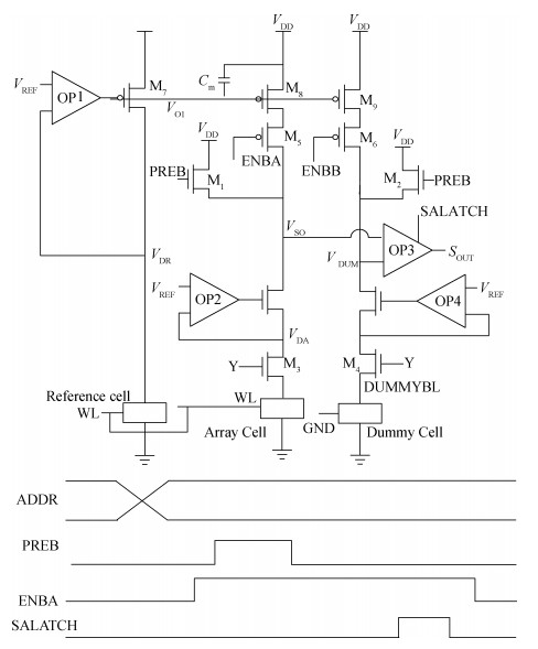
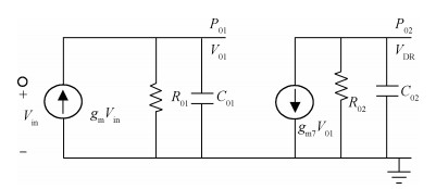
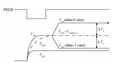
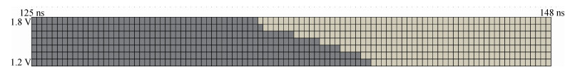
A low-voltage sense amplifier with reference current generator utilizing two-stage operational amplifier clamp structure for flash memory is presented in this paper, capable of operating with minimum supply voltage at 1 V. A new reference current generation circuit composed of a reference cell and a two-stage operational amplifier clamping the drain pole of the reference cell is used to generate the reference current, which avoids the threshold limitation caused by current mirror transistor in the traditional sense amplifier. A novel reference voltage generation circuit using dummy bit-line structure without pull-down current is also adopted, which not only improves the sense window enhancing read precision but also saves power consumption. The sense amplifier was implemented in a flash realized in 90 nm flash technology. Experimental results show the access time is 14.7 ns with power supply of 1.2 V and slow corner at 125 ℃.

J. Semicond.
2017, 38(4): 045002 doi: 10.1088/1674-4926/38/4/045002
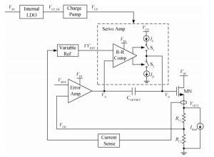
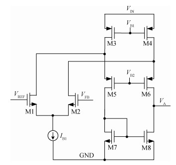
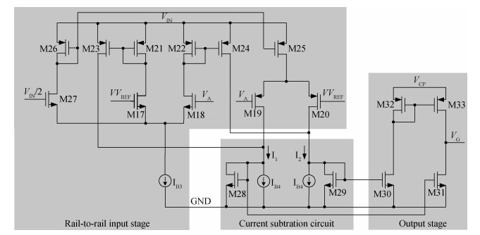
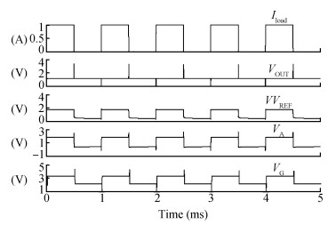
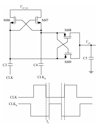
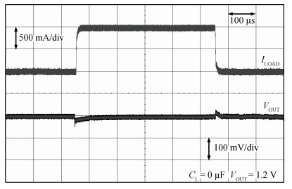
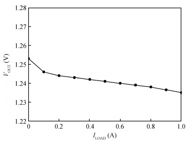
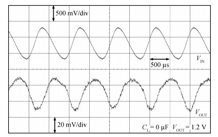
This paper presents a fully on-chip NMOS low-dropout regulator (LDO) for portable applications with quasi floating gate pass element and fast transient response. The quasi floating gate structure makes the gate of the NMOS transistor only periodically charged or refreshed by the charge pump, which allows the charge pump to be a small economical circuit with small silicon area. In addition, a variable reference circuit is introduced enlarging the dynamic range of error amplifier during load transient. The proposed LDO has been implemented in a 0.35 μm BCD process. From experimental results, the regulator can operate with a minimum dropout voltage of 250 mV at a maximum 1 A load and IQ of 395 μA. Under full-range load current step, the voltage undershoot and overshoot of the proposed LDO are reduced to 50 and 26 mV, respectively.


J. Semicond.
2017, 38(4): 045003 doi: 10.1088/1674-4926/38/4/045003
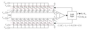
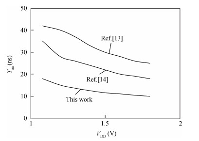
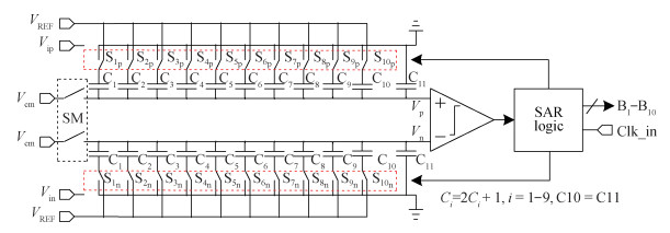
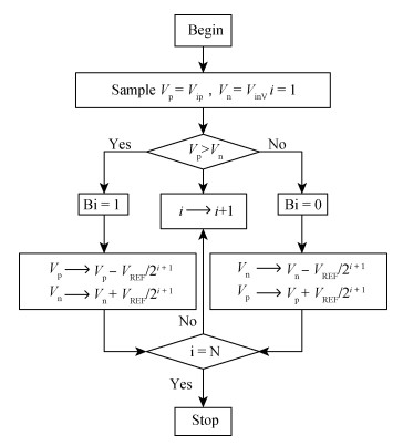
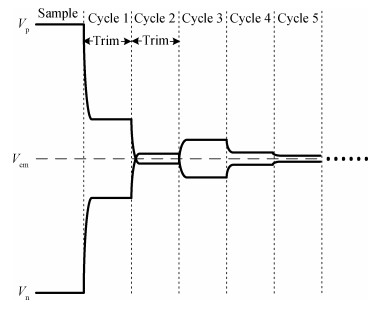
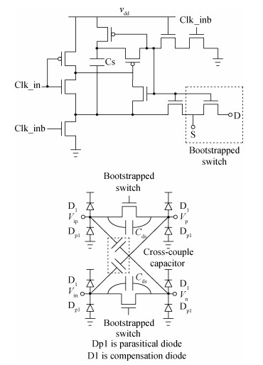
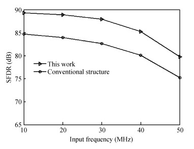
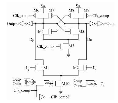
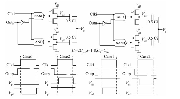
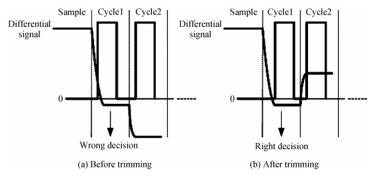
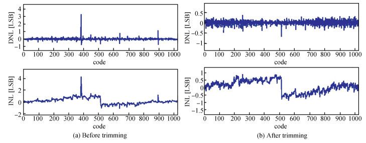
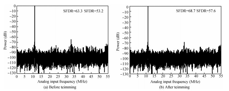
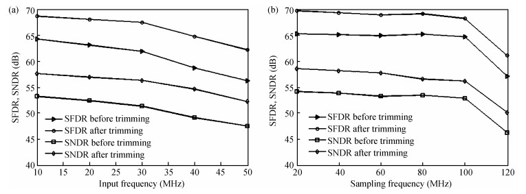
A 10-bit 110 MHz SAR ADC with asynchronous trimming is presented. In this paper, a high linearity sampling switch is used to produce a constant parasitical barrier capacitance which would not change with the range of input signals. As a result, the linearity of the SAR ADC will increase with high linearity sampled signals. Farther more, a high-speed and low-power dynamic comparator is proposed which would reduce the comparison time and save power consumption at the same time compared to existing technology. Additionally, the proposed comparator provides a better performance with the decreasing of power supply. Moreover, a highspeed successive approximation register is exhibited to speed up the conversion time and will reduce about 50% register delay. Lastly, an asynchronous trimming method is provided to make the capacitive-DAC settle up completely instead of using the redundant cycle which would prolong the whole conversion period. This SAR ADC is implemented in 65-nm CMOS technology the core occupies an active area of only 0.025 mm2 and consumes 1.8 mW. The SAR ADC achieves SFDR > 68 dB and SNDR > 57 dB, resulting in the FOM of 28 fJ/conversion-step. From the test results, the presented SAR ADC provides a better FOM compared to previous research and is suitable for a kind of ADC IP in the design SOC.


J. Semicond.
2017, 38(4): 046001 doi: 10.1088/1674-4926/38/4/046001
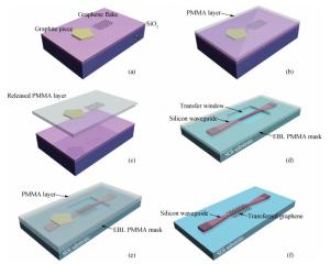
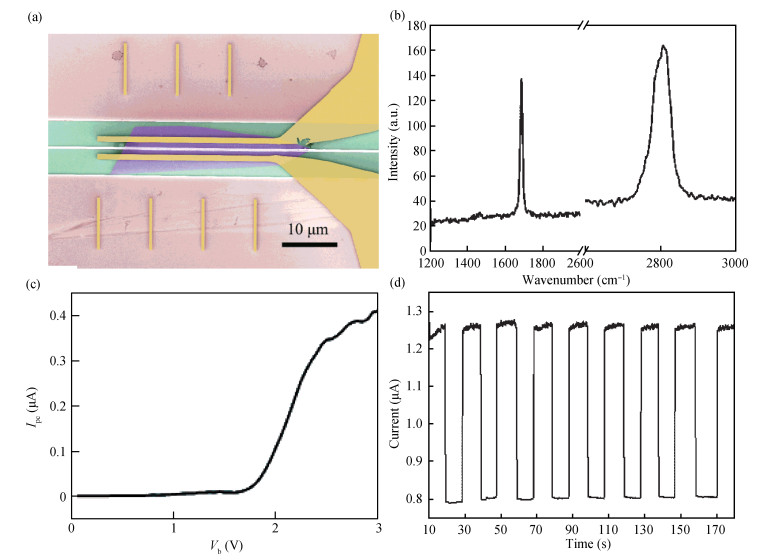
Graphene field-effect transistors have been intensively studied. However, in order to fabricate devices with more complicated structures, such as the integration with waveguide and other two-dimensional materials, we need to transfer the exfoliated graphene samples to a target position. Due to the small area of exfoliated graphene and its random distribution, the transfer method requires rather high precision. In this paper, we systematically study a method to selectively transfer mechanically exfoliated graphene samples to a target position with a precision of sub-micrometer. To characterize the doping level of this method, we transfer graphene flakes to pre-patterned metal electrodes, forming graphene field-effect transistors. The hole doping of graphene is calculated to be 2.16 × 1012 cm-2. In addition, we fabricate a waveguide-integrated multilayer graphene photodetector to demonstrate the viability and accuracy of this method. A photocurrent as high as 0.4 μA is obtained, corresponding to a photoresponsivity of 0.48 mA/W. The device performs uniformly in nine illumination cycles.