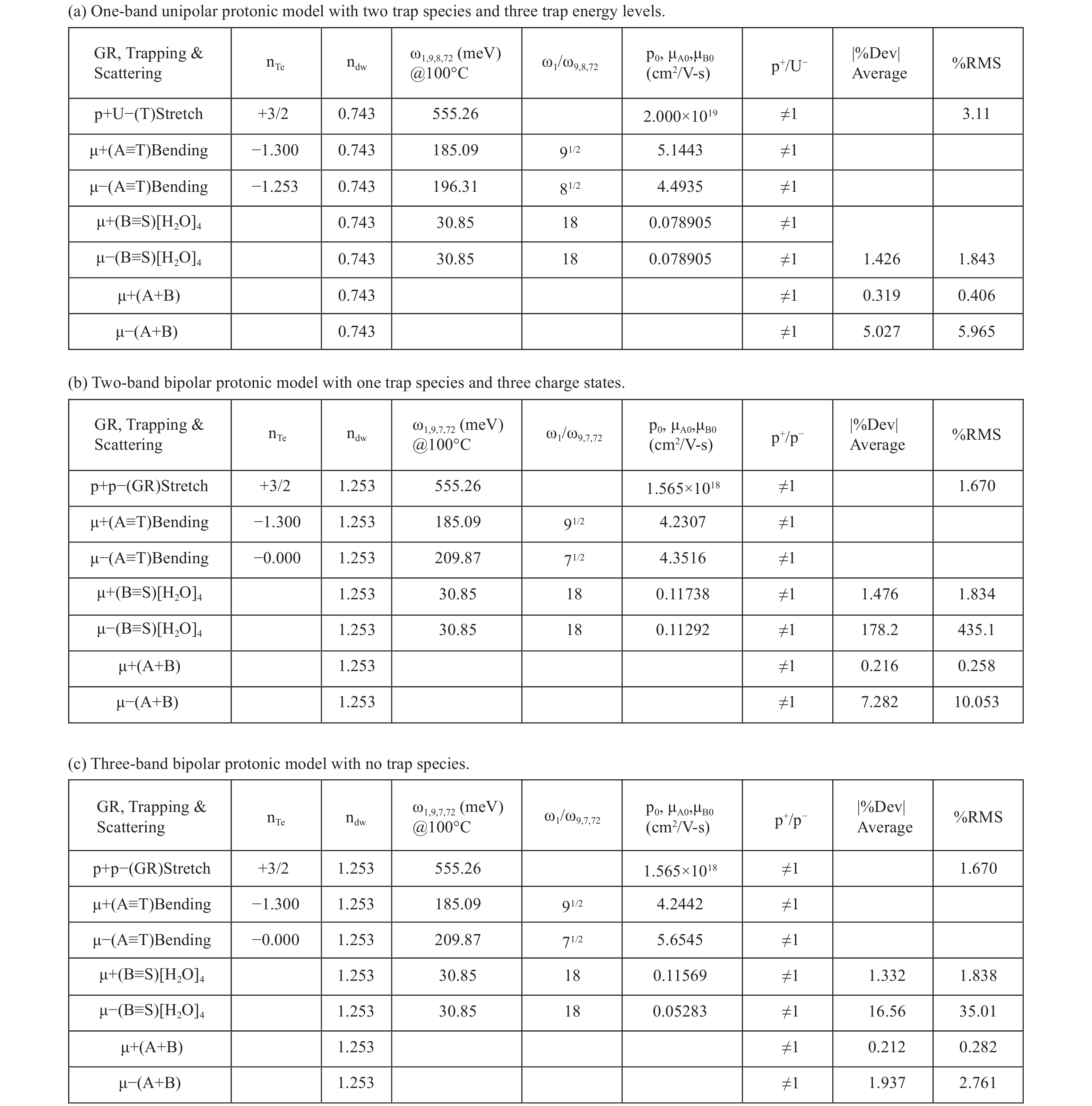
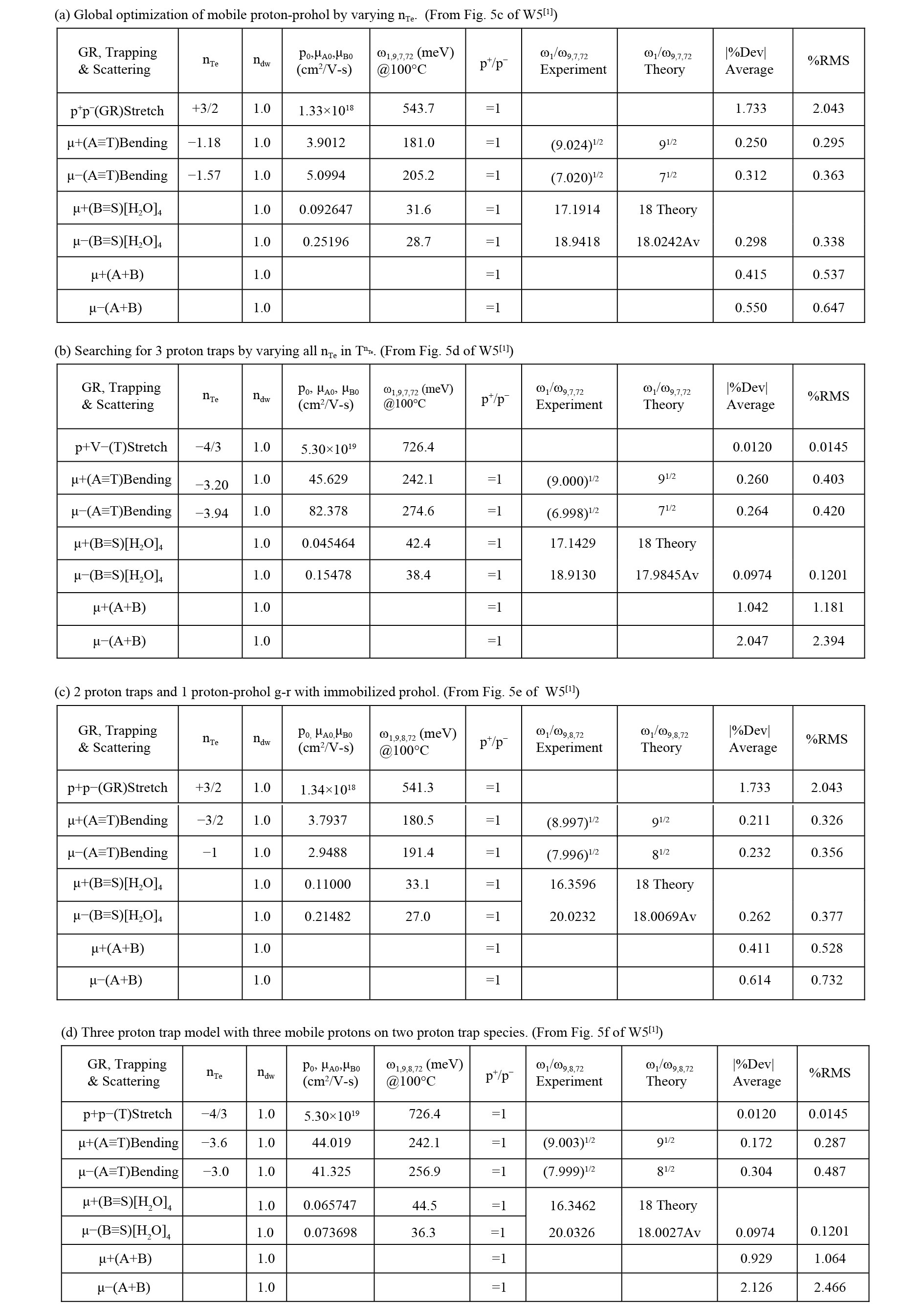
This report adds three protonic semiconductor models to explain the " abnormally” high electrical conductivity of pure liquid water characterized by the three industrial consensus parameters, the ion product (or pH) and the two ion mobilities. Existence of long-range order in fluid water under numerous daily conditions led us to extend the 1933 Bernal-Fowler hexagonally close packed crystalline Ice Lattice to model liquid water as Melted Ice. Protonic kinetic energy band and bound (trap) pictures provide semiconductor-physics based new models of these three parameters. They are extrapolatable engineered-models for developing novel biological, chemical, electrical, mechanical and medical applications of liquid water.
Issue Browser
Volume 39, Issue 11,
Nov 2018

J. Semicond.
2018, 39(11): 112001 doi: 10.1088/1674-4926/39/11/112001

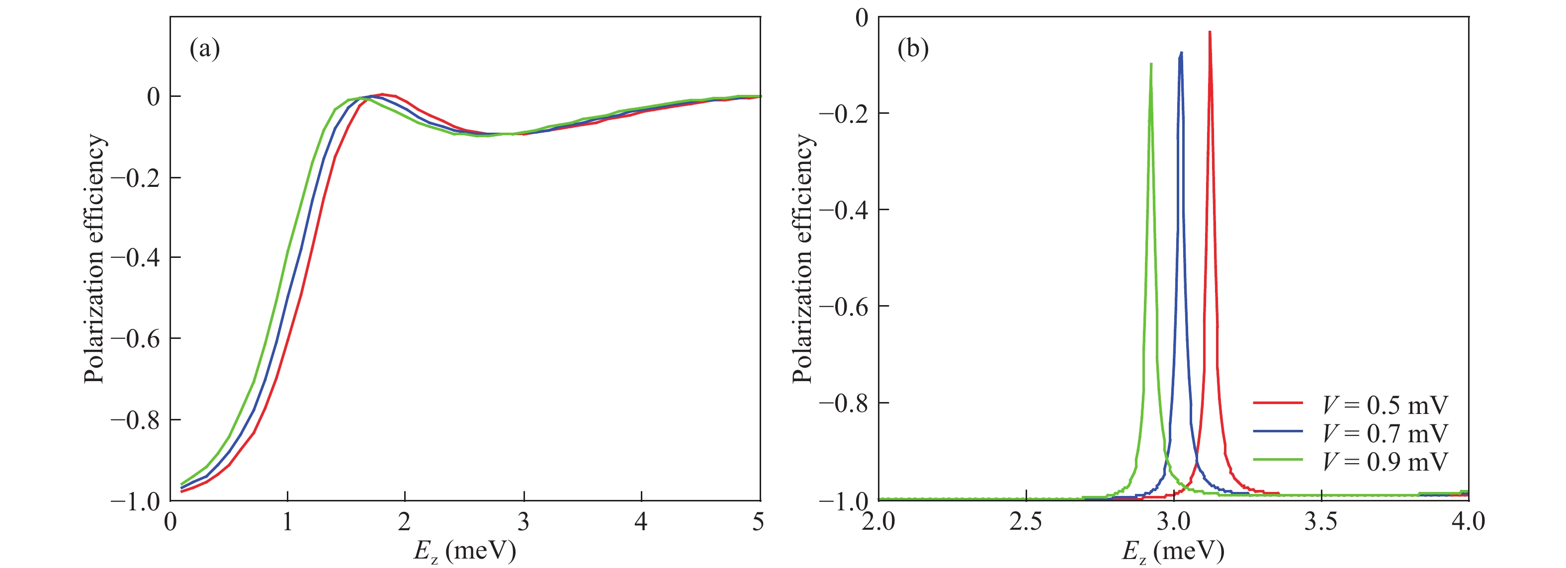
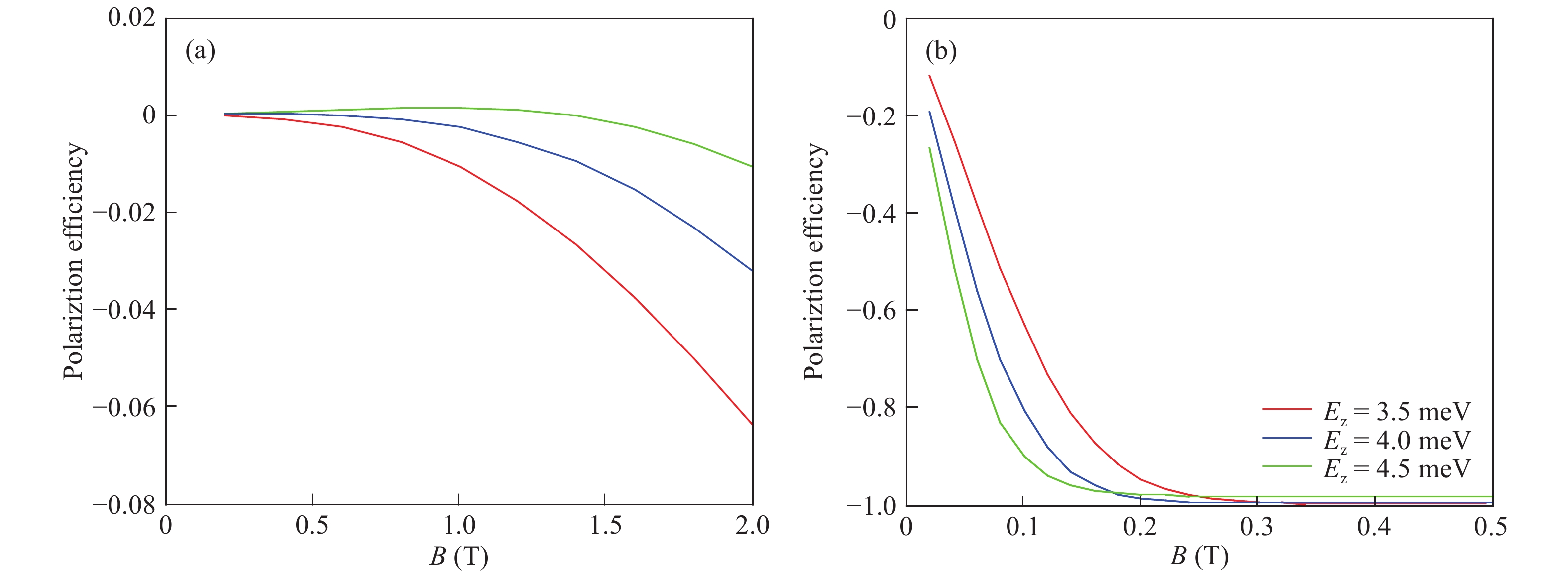
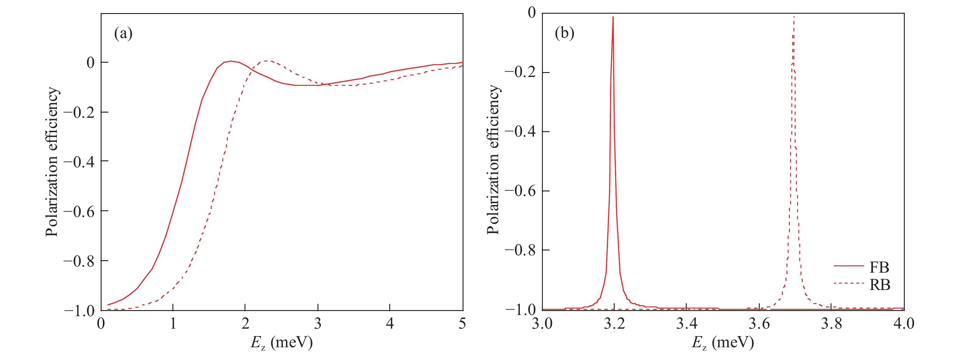
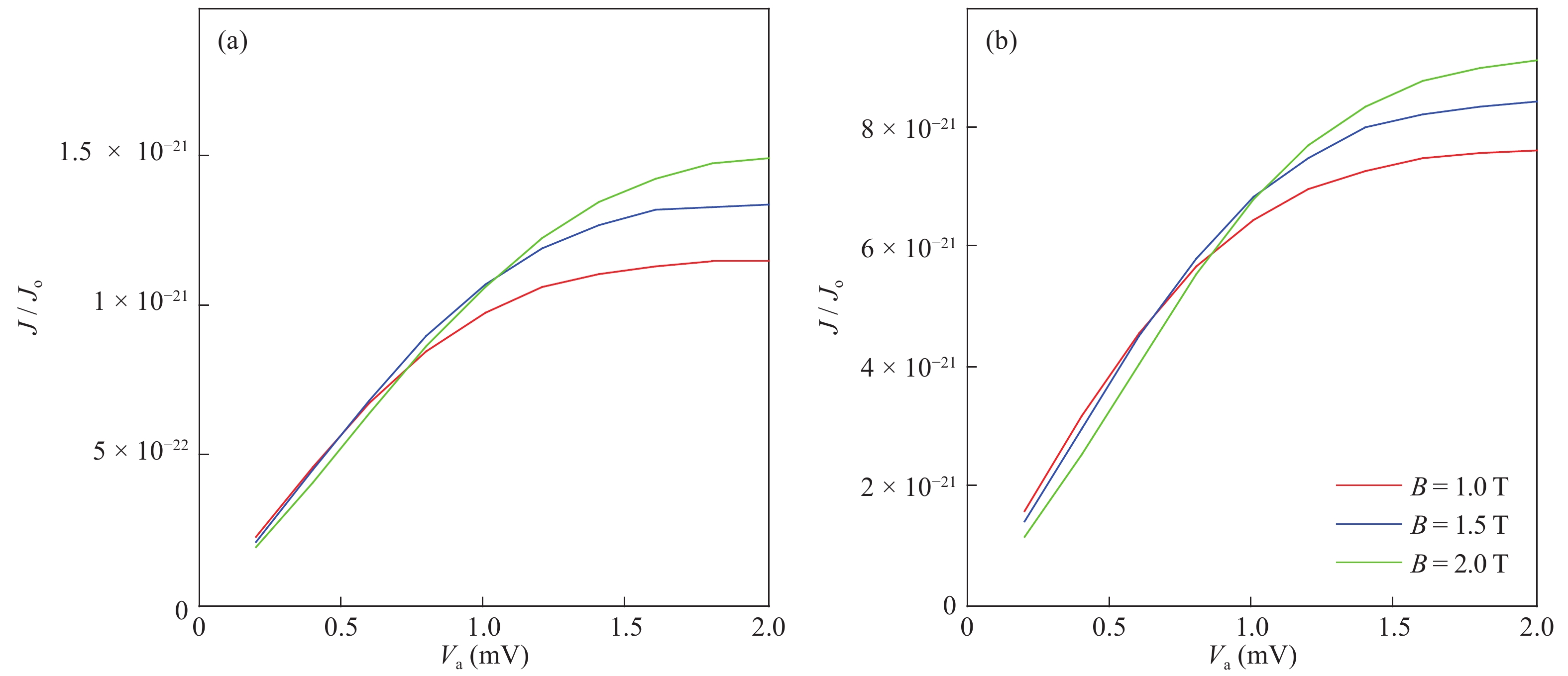
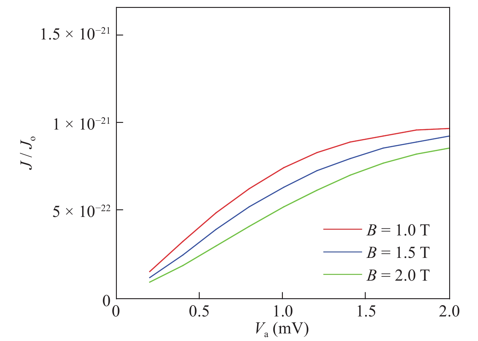
The spin-dependent tunneling of light holes and heavy holes was analysed in a symmetrical heterostructure with externally applied electric and magnetic fields. The effects of the applied bias voltage, magnetic field and reverse bias were discussed for the polarization efficiency of light holes and heavy holes. The current density of spin-up and spin-down light holes increases as the bias voltage increases and reaches the saturation, whereas the current density of spin-up heavy holes is almost negligible. The applied bias voltage and the magnetic field highly influence the energy of resonance polarization, polarization efficiency, and the current density of heavy holes more than for the light holes.
J. Semicond.
2018, 39(11): 113001 doi: 10.1088/1674-4926/39/11/113001
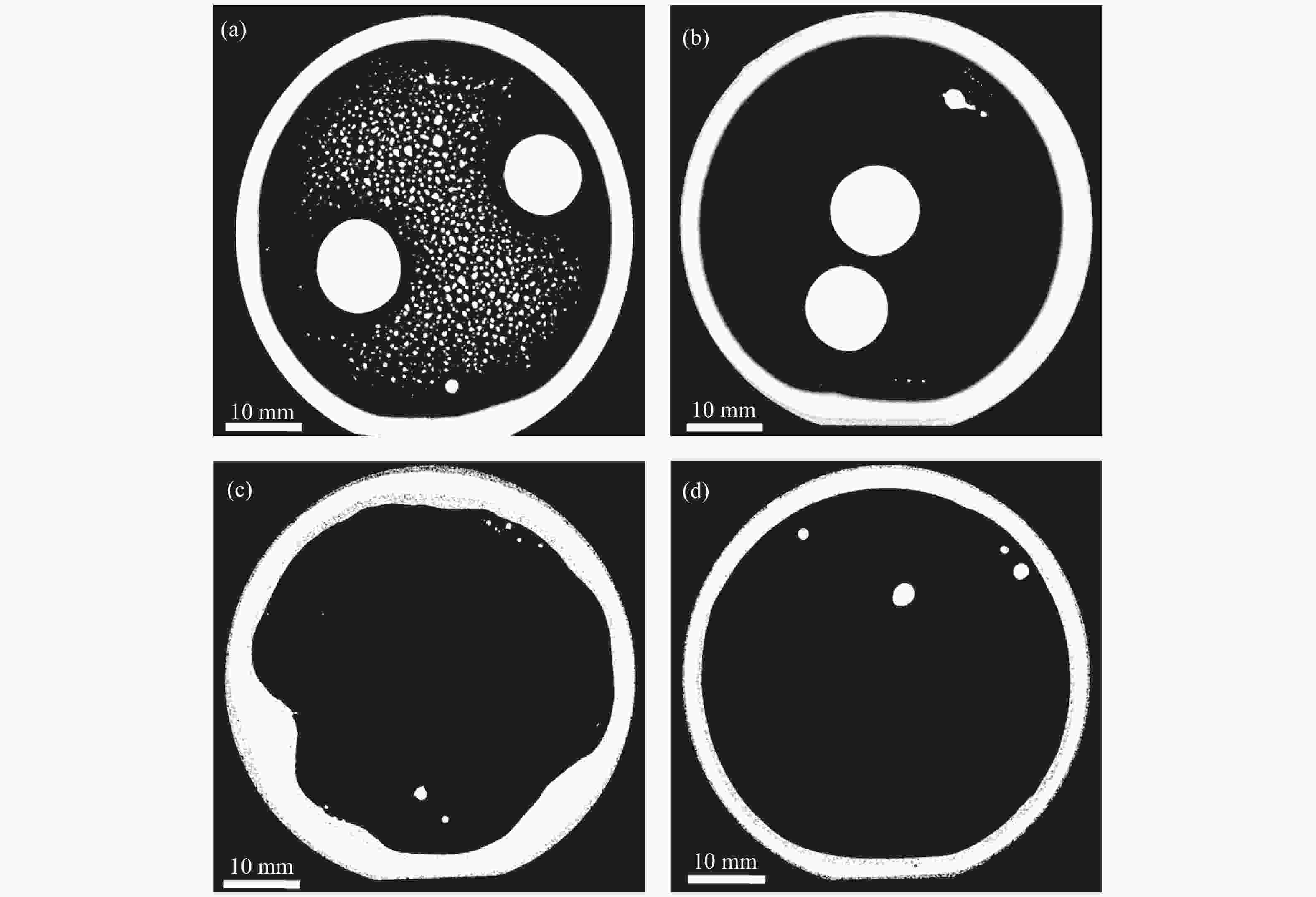
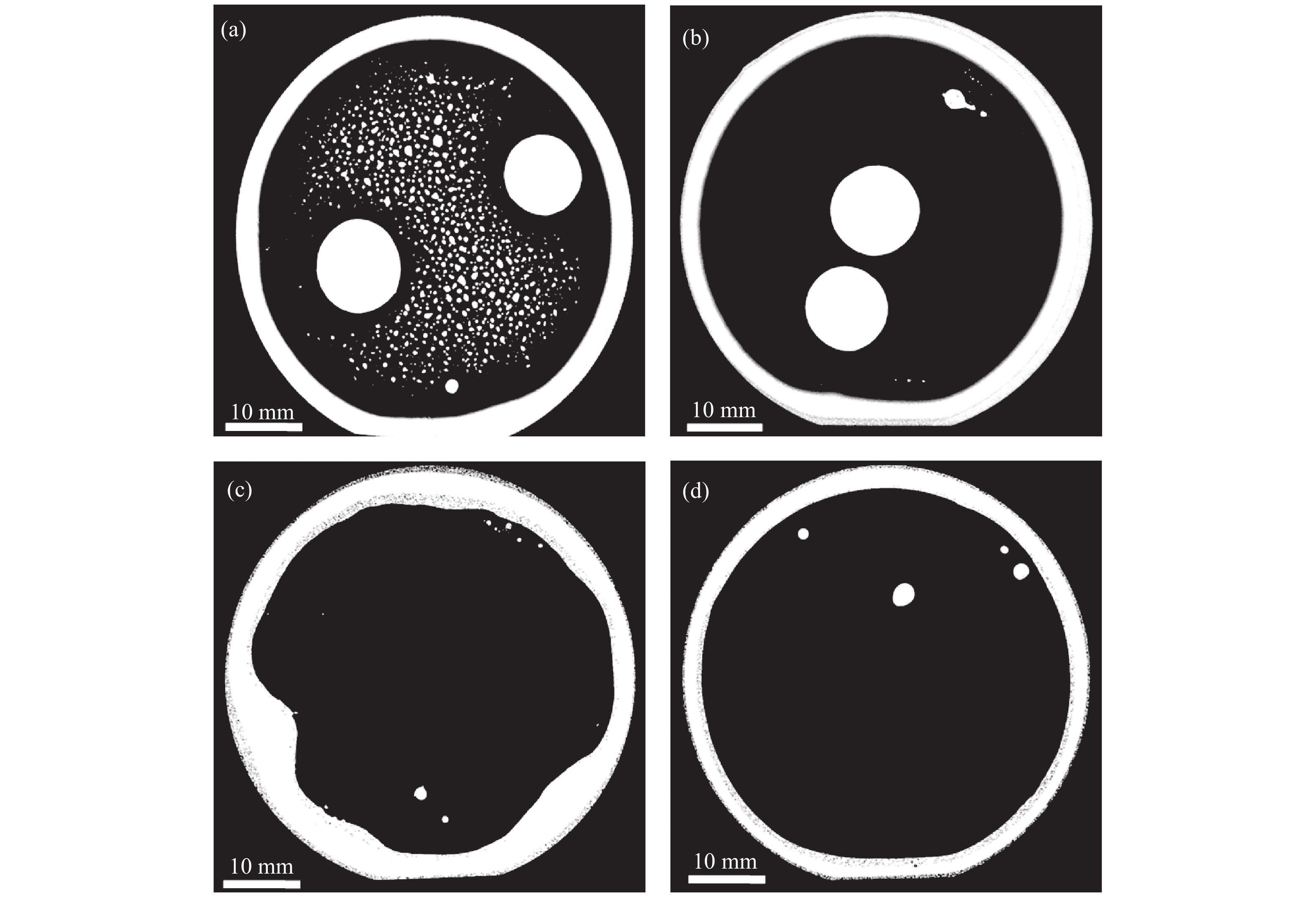
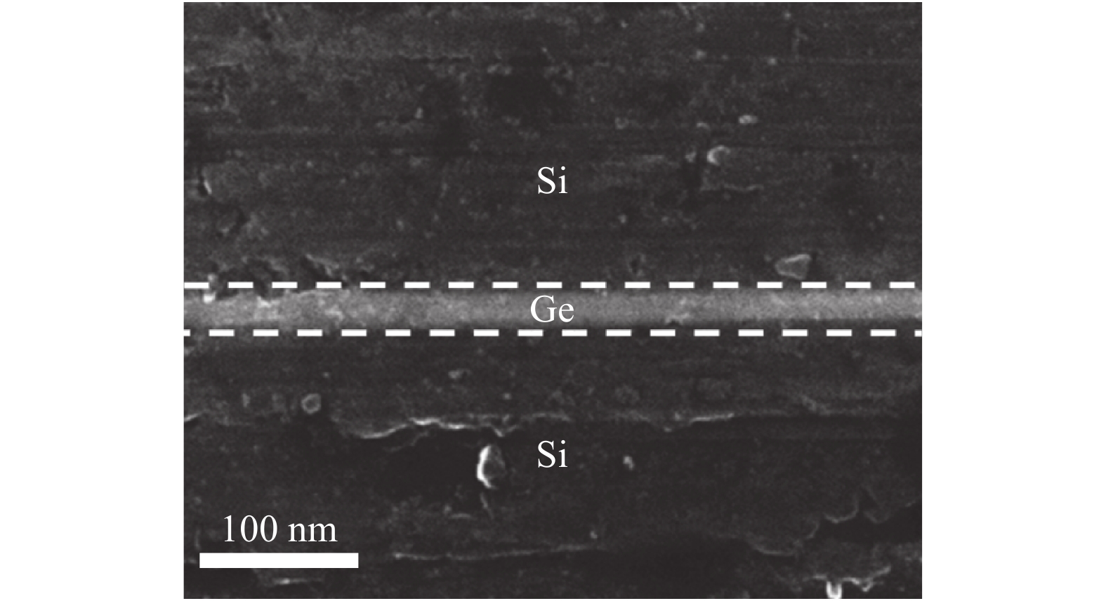
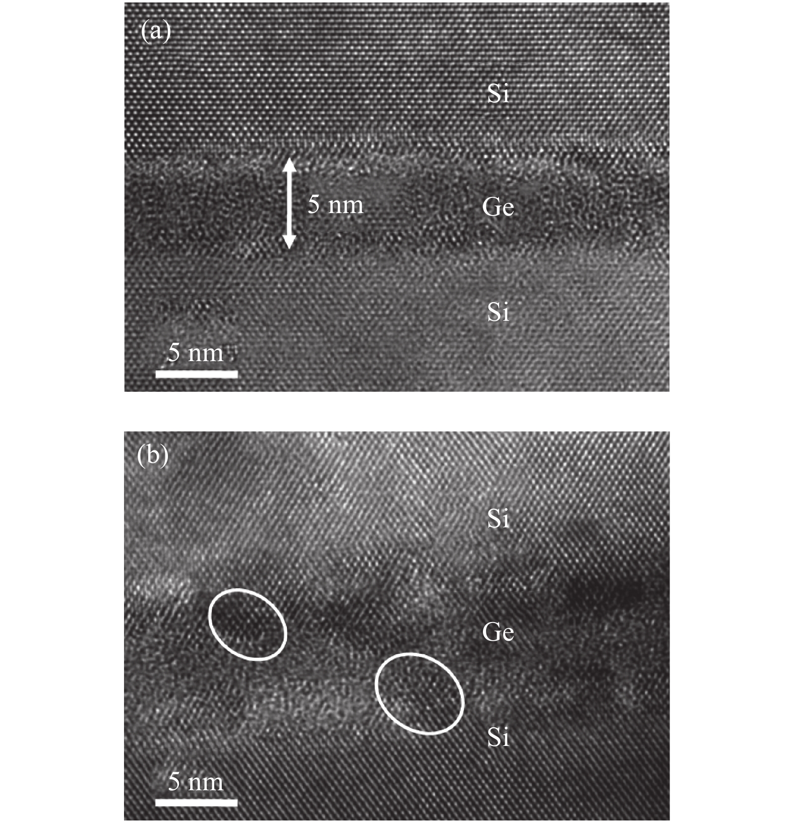
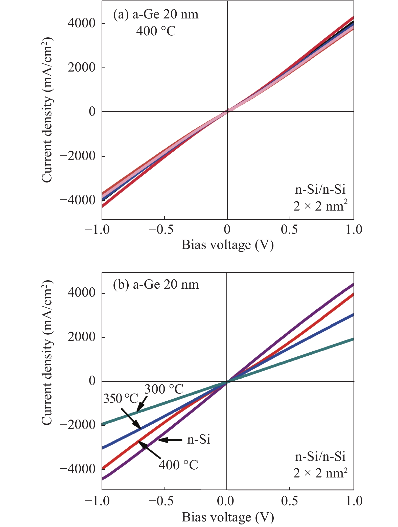
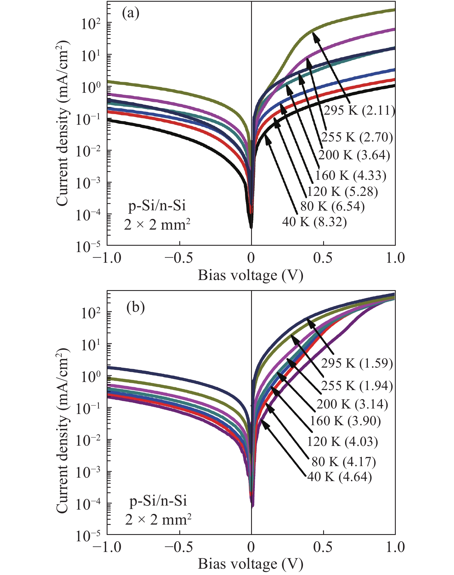
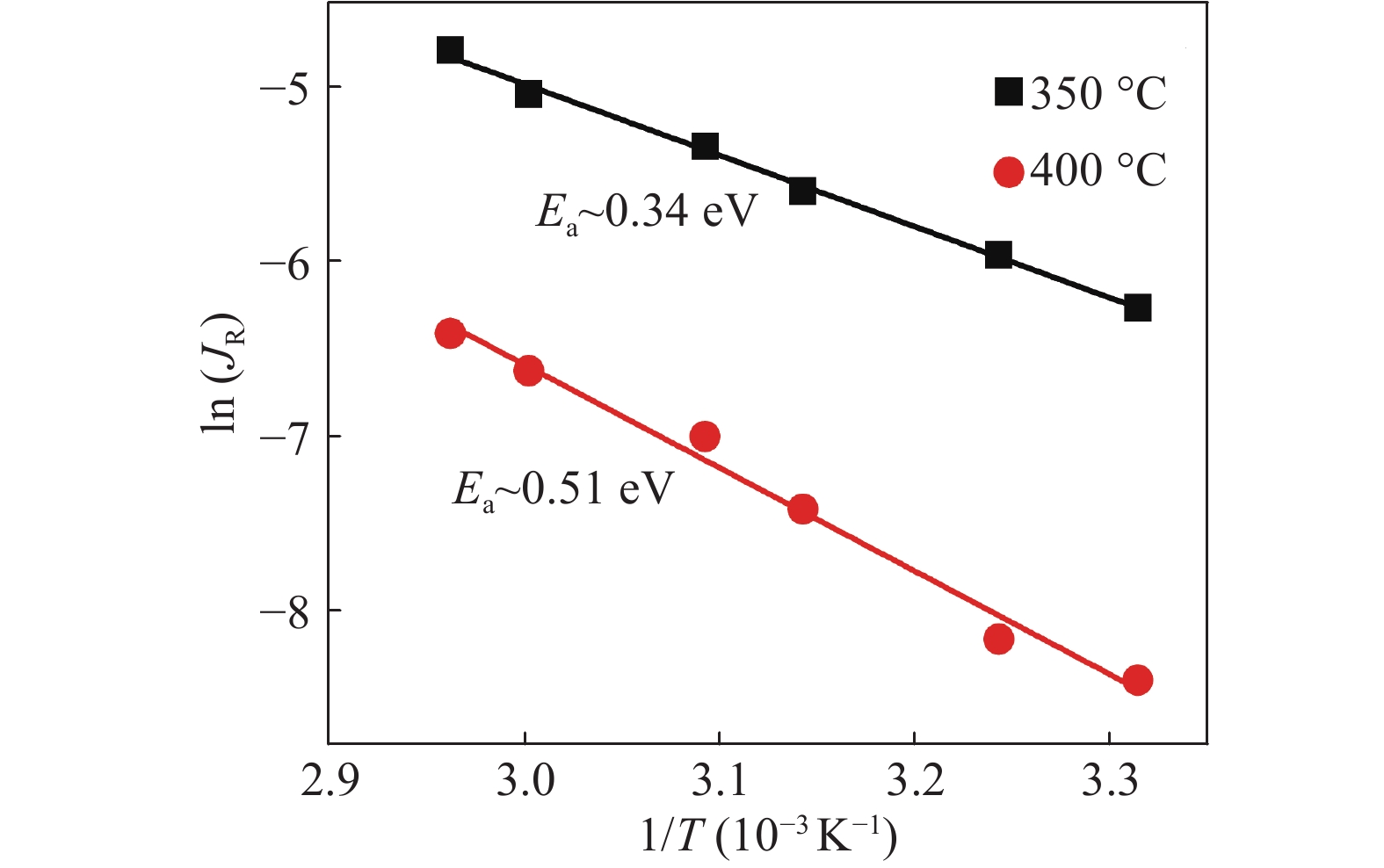
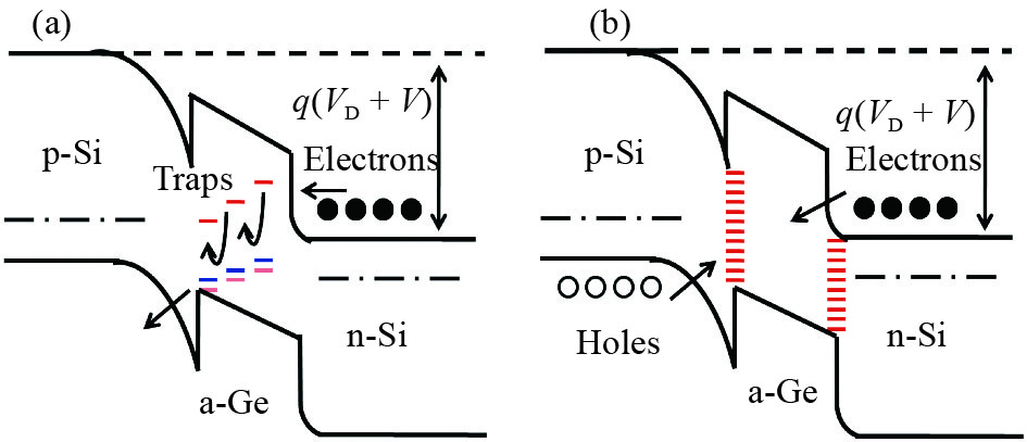
An amorphous Ge (a-Ge) intermediate layer is introduced into the Si bonded interface to lower the annealing temperature and achieve good electrical characteristics. The interface and electrical characteristics of n-Si/n-Si and p-Si/n-Si junctions manufactured by low-temperature wafer bonding based on a thin amorphous Ge are investigated. It is found that the bubble density tremendously decreases when the a-Ge film is not immersed in DI water. This is due to the decrease of the –OH groups. In addition, when the samples are annealed at 400 °C for 20 h, the bubbles totally disappear. This can be explained by the appearance of the polycrystalline Ge (absorption of H2) at the bonded interface. The junction resistance of the n-Si/n-Si bonded wafers decreases with the increase of the annealing temperature. This is consistent with the recrystallization of the a-Ge when high-temperature annealing is conducted. The carrier transport of the Si-based PN junction annealed at 350 °C is consistent with the trap-assisted tunneling model and that annealed at 400 °C is related to the carrier recombination model.

J. Semicond.
2018, 39(11): 113002 doi: 10.1088/1674-4926/39/11/113002
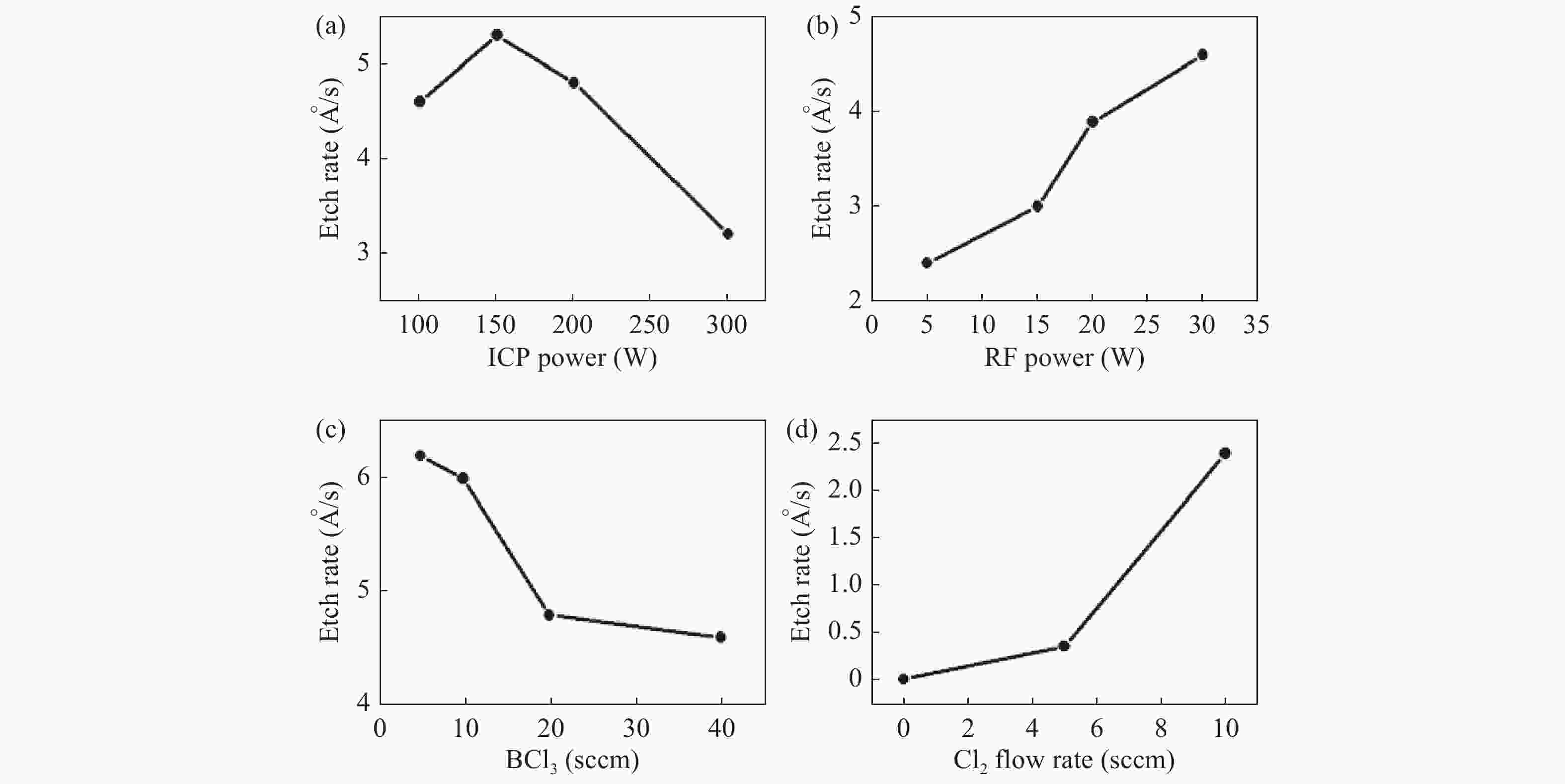
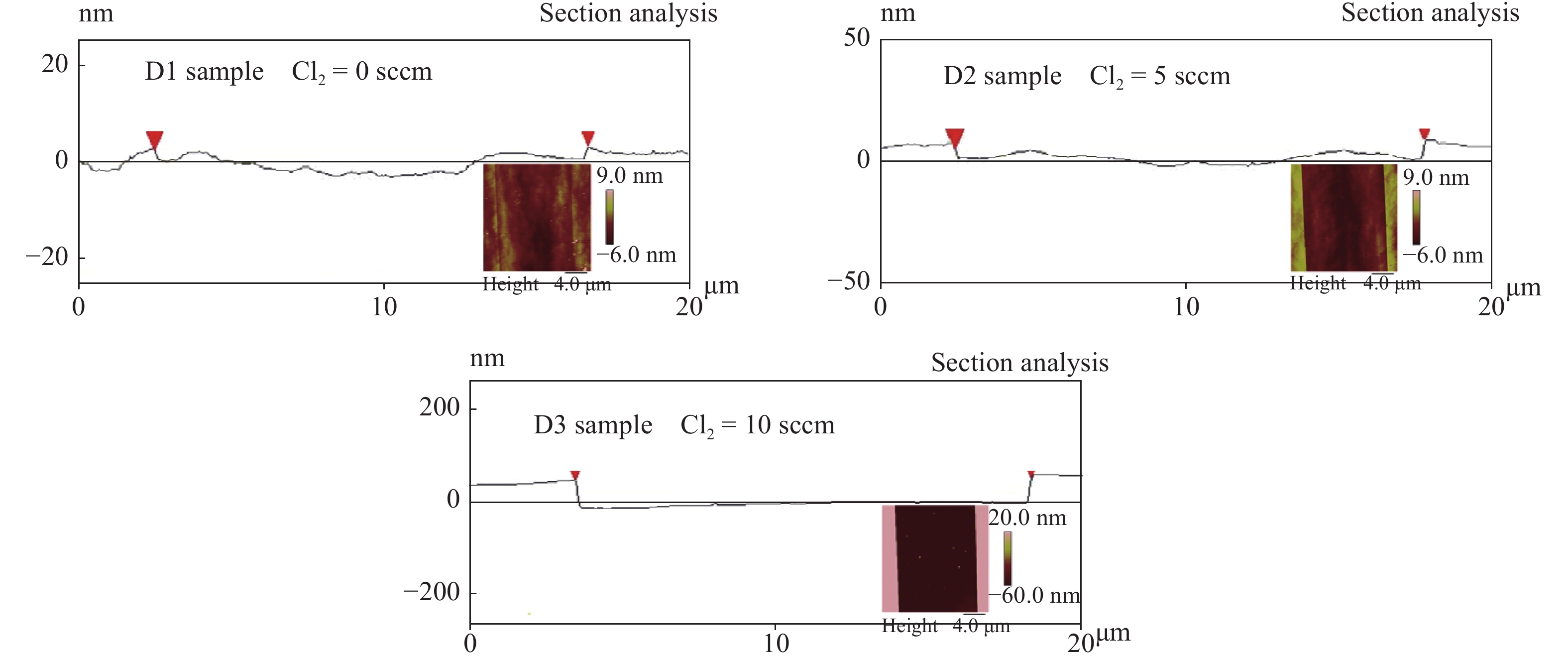
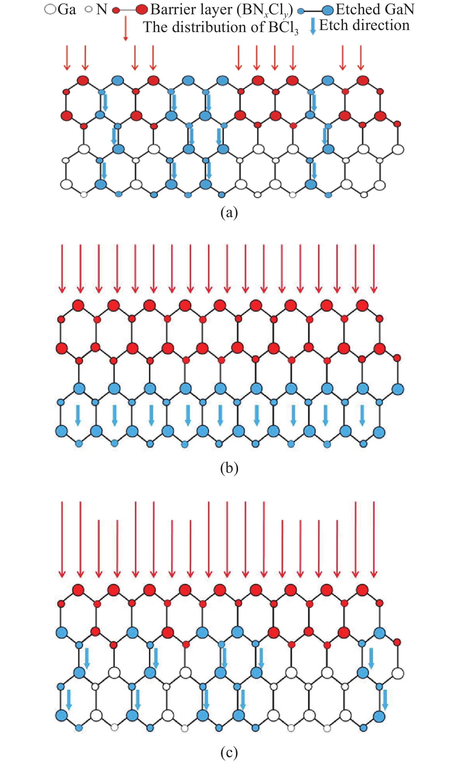
Slow and smooth etching of gallium nitride (GaN) by BCl3/Cl2-based inductively coupled plasma (ICP) is investigated in this paper. The effects of etch parameters, including ICP power, radio frequency (RF) power, the flow rate of Cl2 and BCl3, on GaN etch rate and etch surface roughness RMS are discussed. A new model is suggested to explain the impact mechanism of the BCl3 flow rate on etch surface roughness. An optimized etch result of a slow and smooth etch surface was obtained; the etch rate and RMS were 0.36 Å/s and 0.9 nm, respectively.


J. Semicond.
2018, 39(11): 114001 doi: 10.1088/1674-4926/39/11/114001
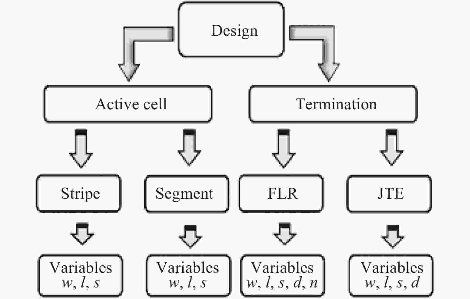
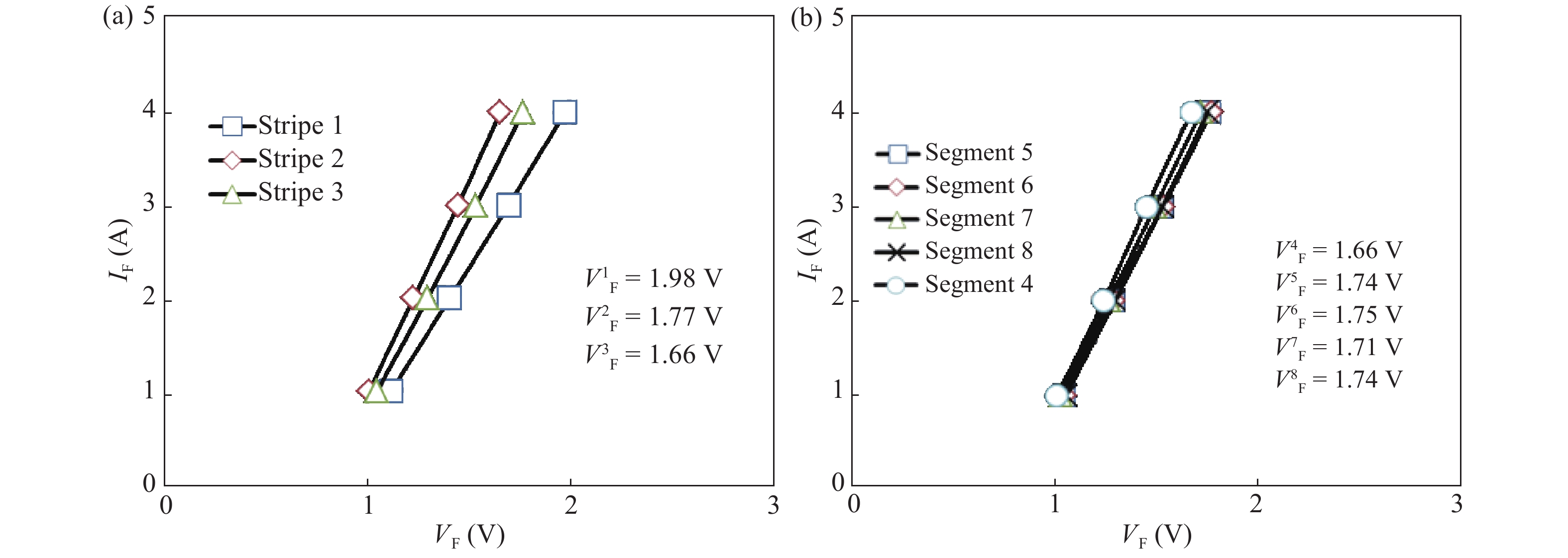
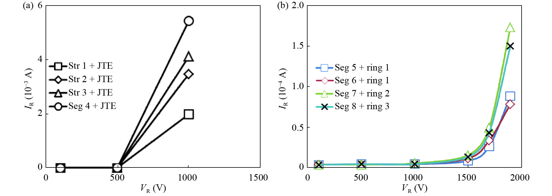
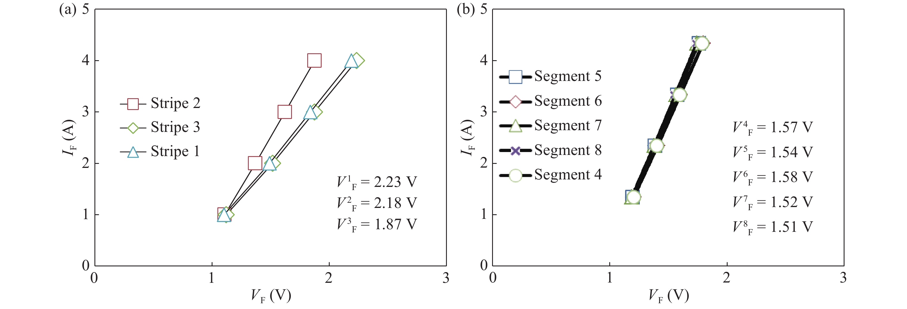
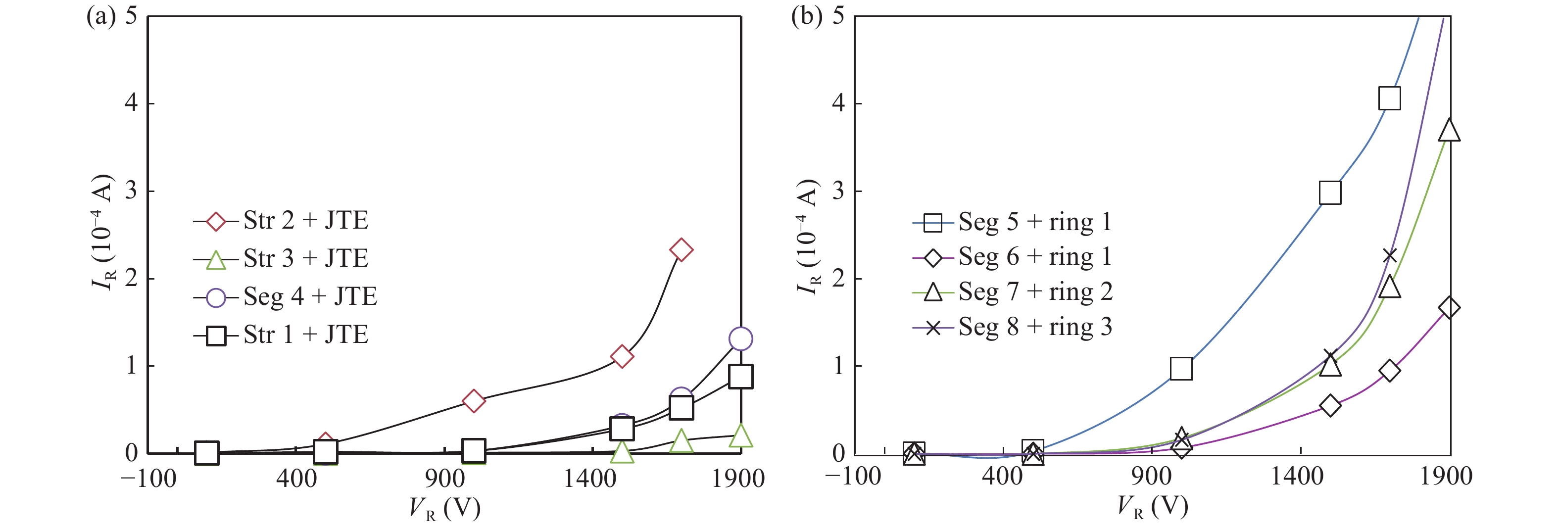
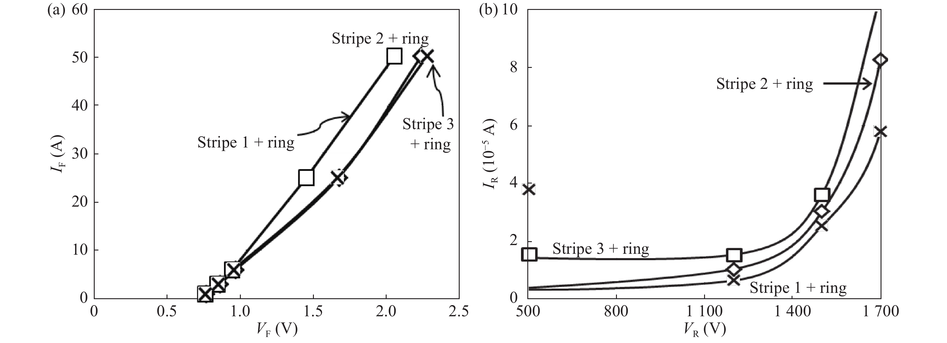
We have studied the influence of design and process variations on the electrical performance of SiC Schottky diodes. On the design side, two design variations are used in the active cell of the diode (segment design and stripe design). In addition, there are two more design variations employed for the edge termination layout of the diodes, namely, field limiting ring (FLR) and junction termination extension (JTE). On the process side, some diodes have gone through an N2O annealing step. The segment design resulted in a lower forward voltage drop (VF) in the diodes and the FLR design turned out to be a better choice for blocking voltages, in the reverse bias. Also, N2O annealing has shown a detrimental effect on the diodes’ blocking performance, which have JTE as their termination design. It degrades the blocking capability of the diodes significantly.


J. Semicond.
2018, 39(11): 114002 doi: 10.1088/1674-4926/39/11/114002
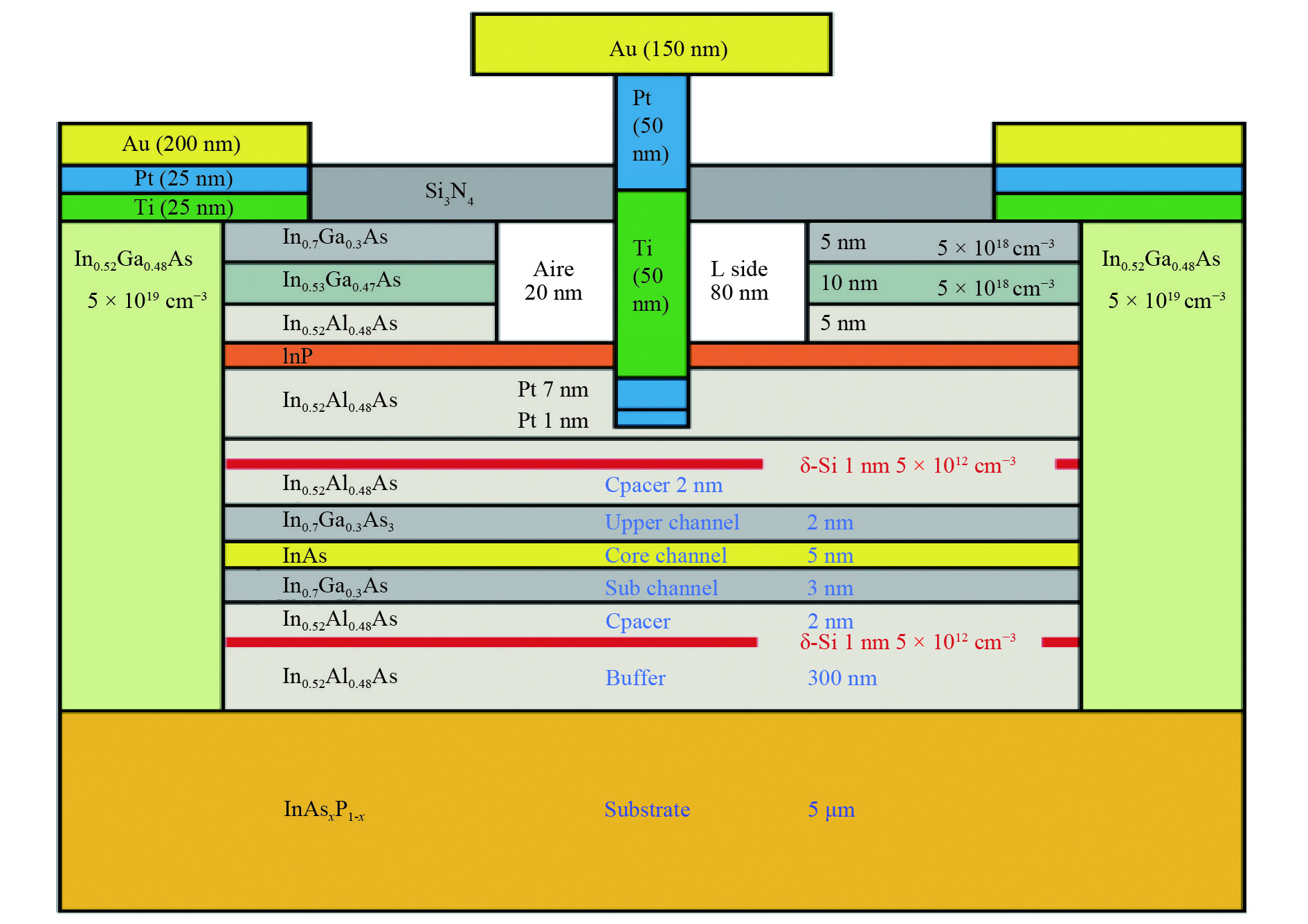
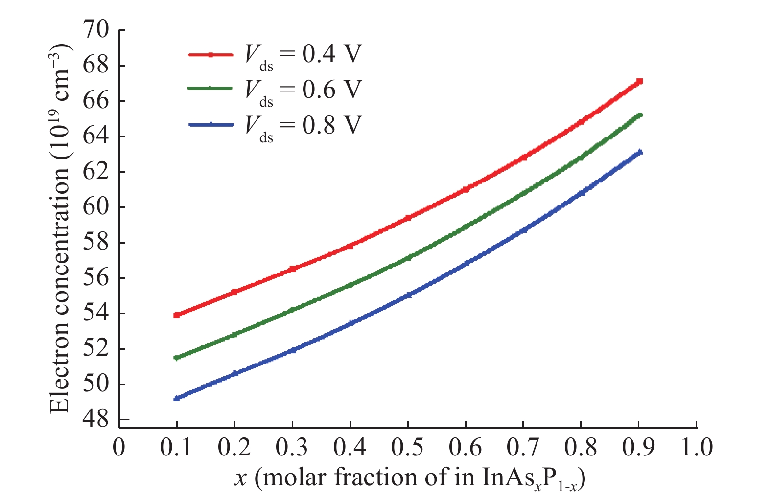
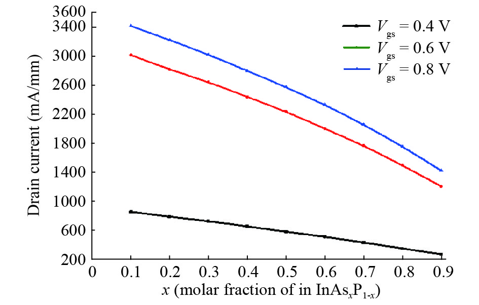
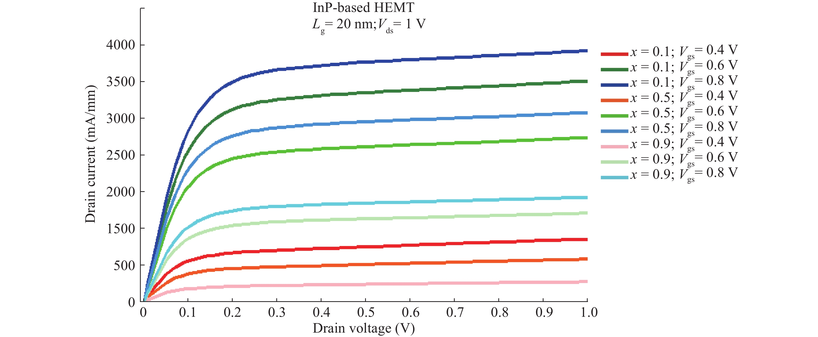
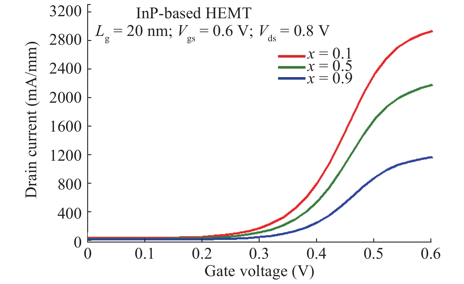
We present the drain current modulation for an HEMT using the TCAD SILVACO simulation tool with a drift–diffusion model at ambient temperature. The obtained results show that the decreases of substrate energies induce the decreasing of the obtained drain current similarly to the transconductance, which described the device due to increasing the transferred electrons concentration towards the substrate region, consequently to increase the molar fraction where the concentration of transferred electrons increases from 49 × 1019 to 65 × 1019 cm−3 when the molar fraction increases from 0.1 to 0.9. On the other hand, the decrease of molar fraction from 0.9 to 0.1 induces the increasing of drain current by 63%, where it increases from 1.1 mA/mm to 3 mA/mm at Vgs = 0.6 V and Vds = 1 V. This fact leads to ensuring the possibility of using the obtained results of this work related to drain current for producing performances devices that brings together the AC characteristics of HEMT with a weak drain current, which is important in the bioengineering domain.


J. Semicond.
2018, 39(11): 114003 doi: 10.1088/1674-4926/39/11/114003
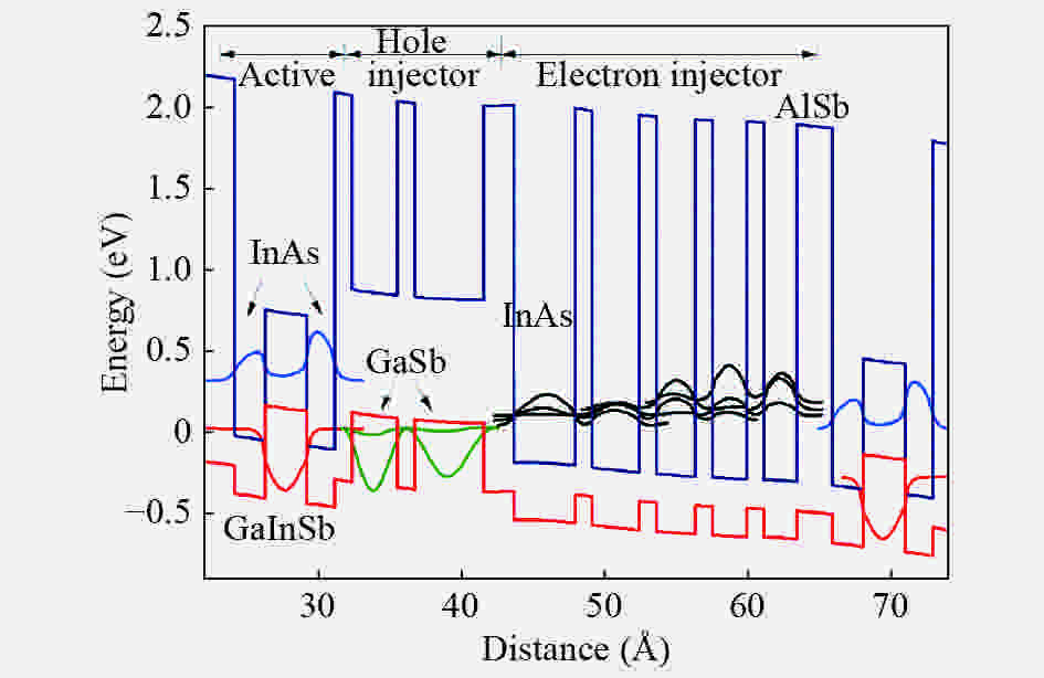
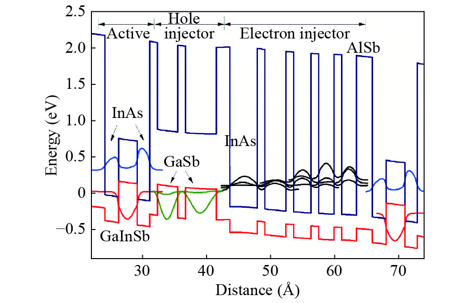
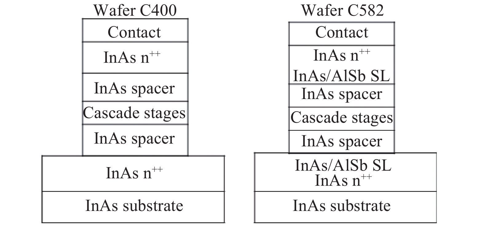
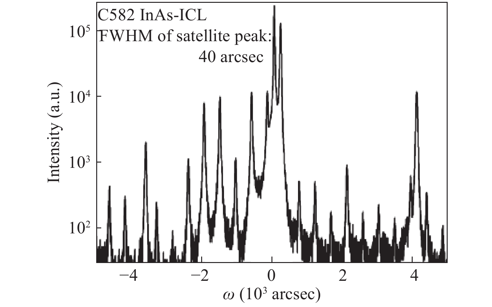
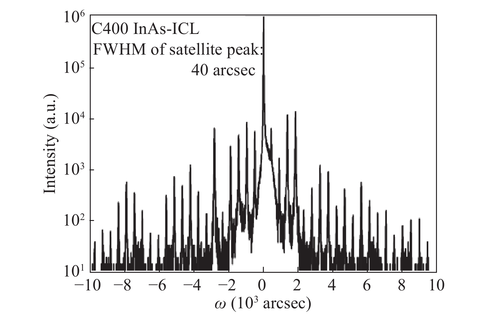
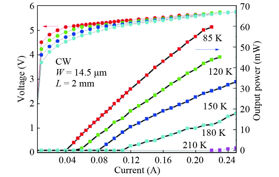
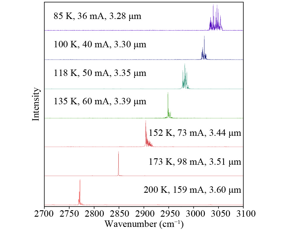
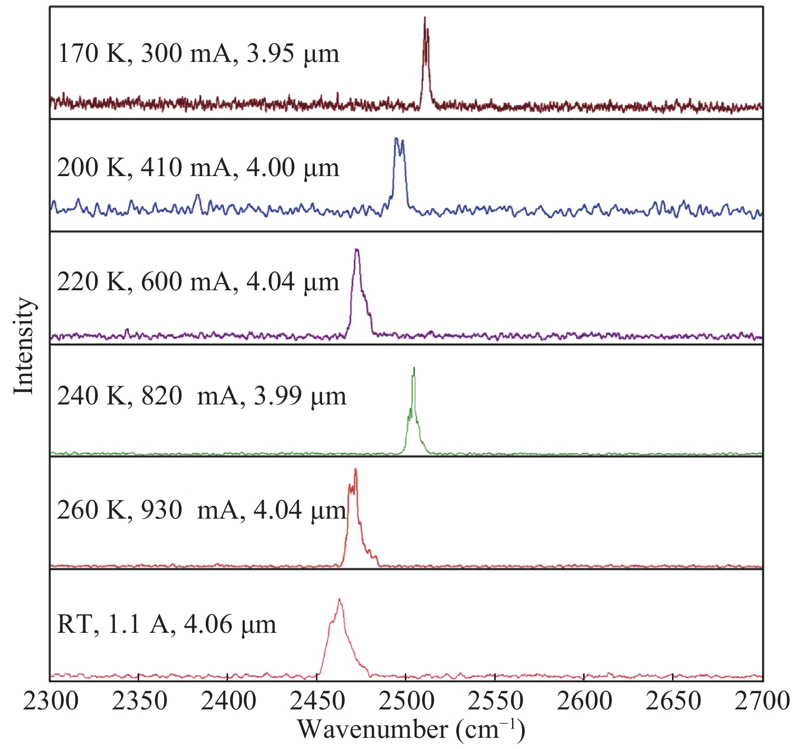
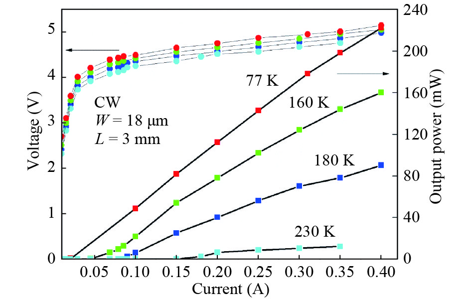
InAs-based interband cascade lasers (ICLs) with InAs plasmon waveguides or InAs/AlSb superlattice (SL) waveguides were demonstrated at emission wavelengths below 4.1 μm. The threshold current densities of the lasers with SL waveguides were 37 A/cm2 at 77 K in continuous wave mode. The operation temperature of these lasers reached room temperature in pulsed mode. Compared with the thick InAs n++ plasmon cladding layer, the InAs/AlSb superlattice cladding layers have greater advantages for ICLs with wavelengths less than 4 μm even in InAs based ICLs because in the short-wavelength region they have a higher confinement factor than InAs plasmon waveguides.

J. Semicond.
2018, 39(11): 114004 doi: 10.1088/1674-4926/39/11/114004
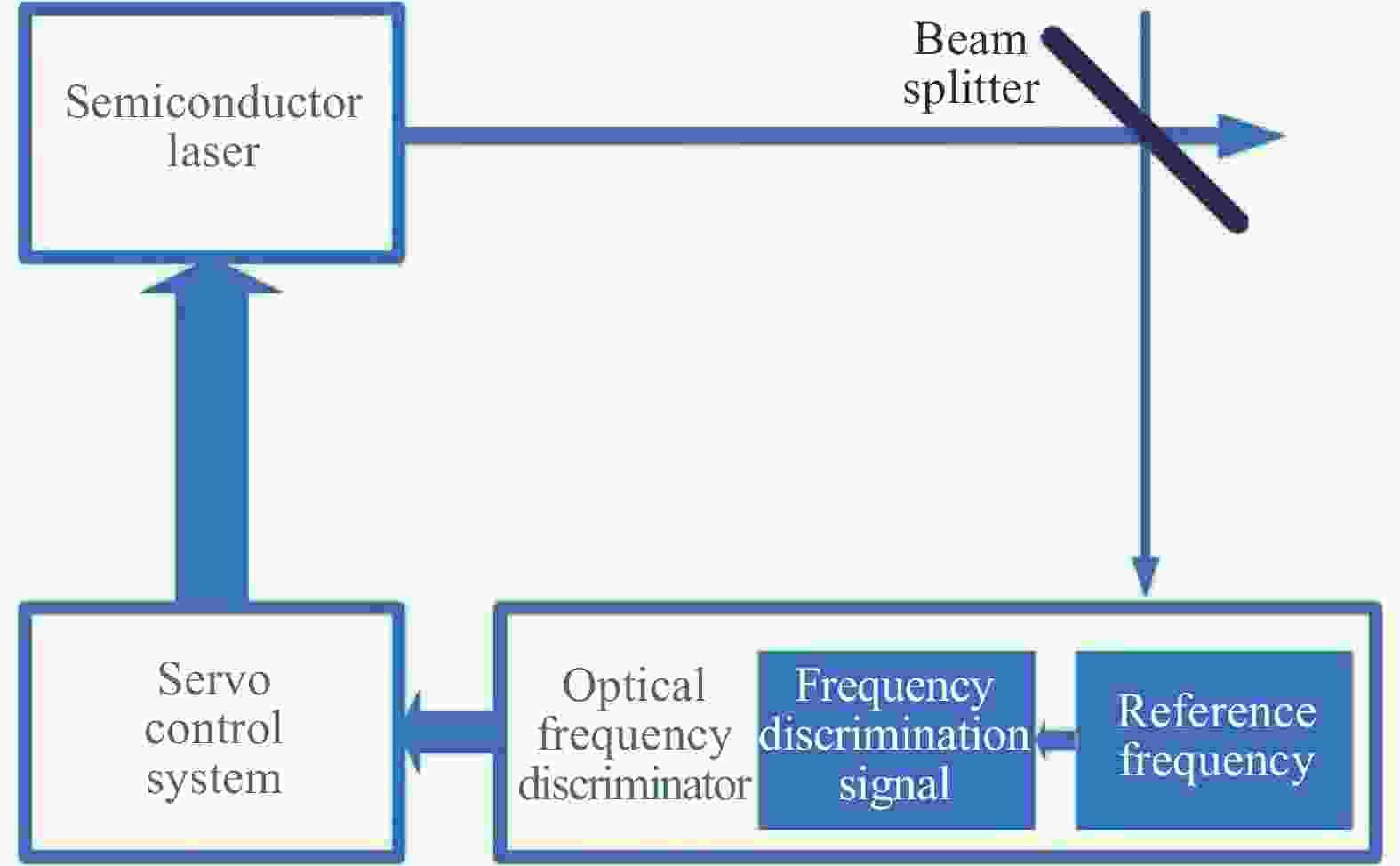
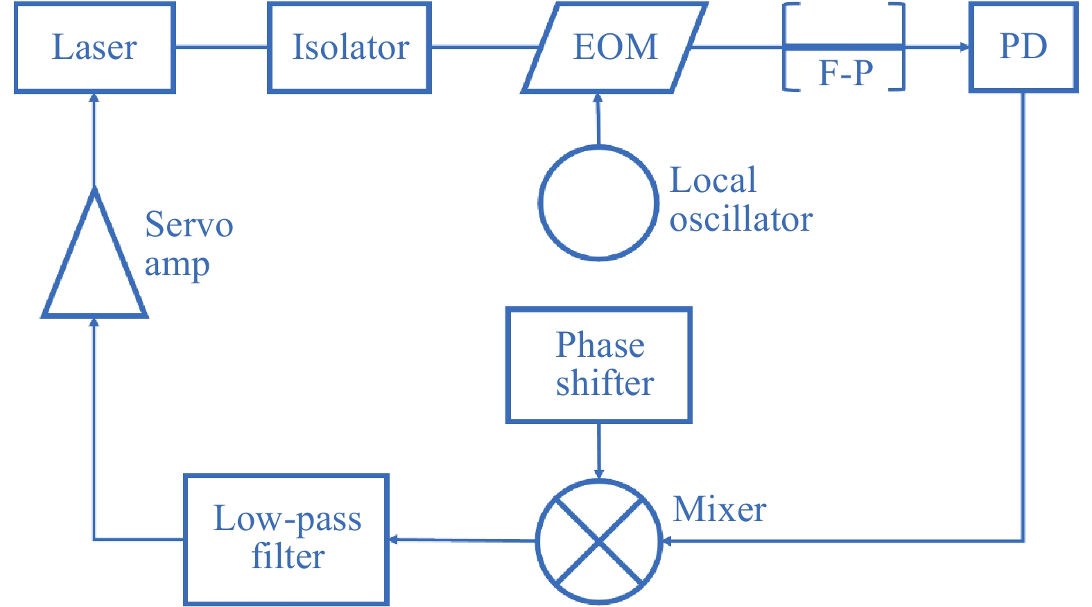
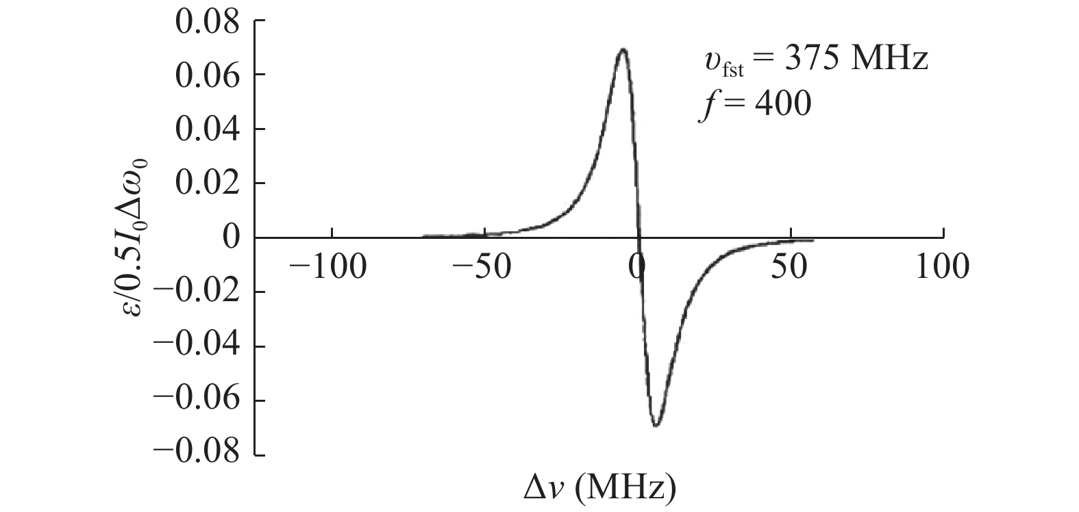
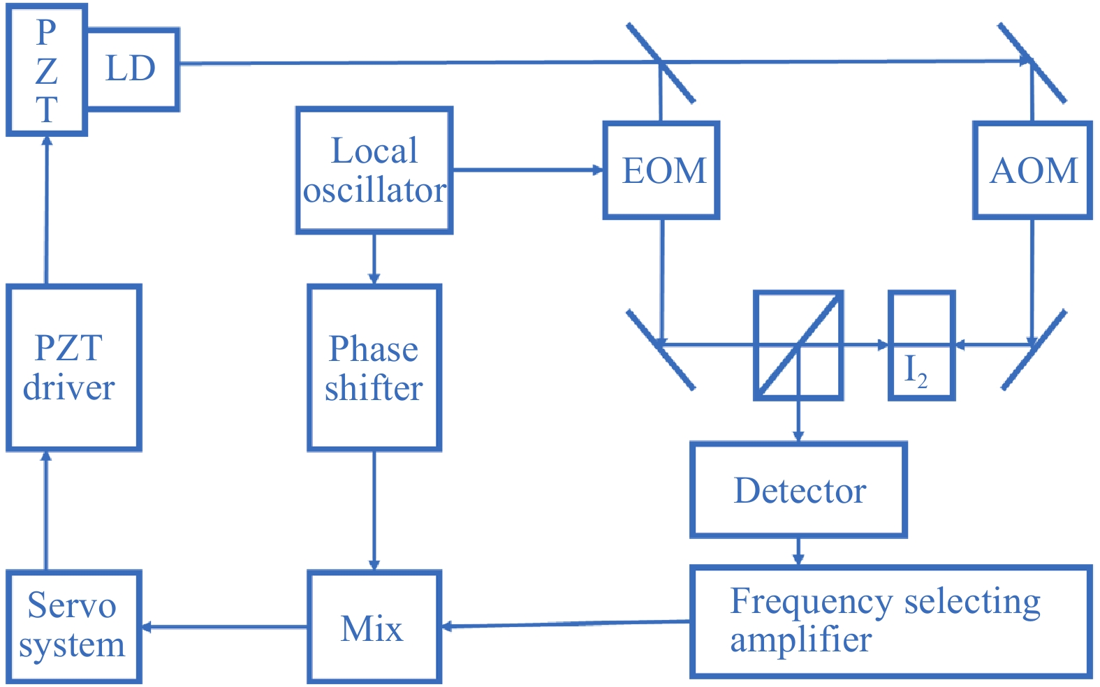
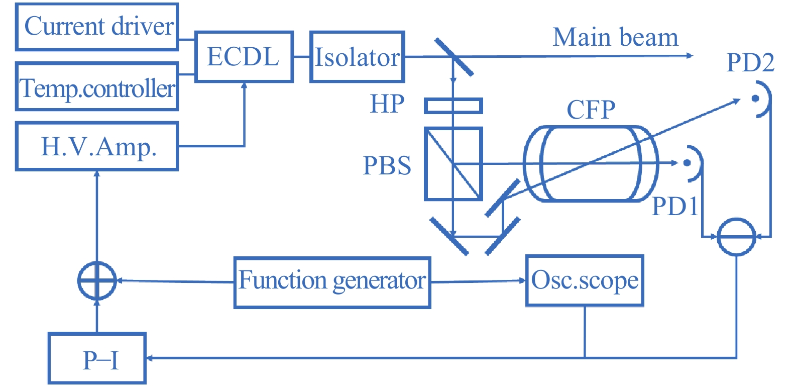
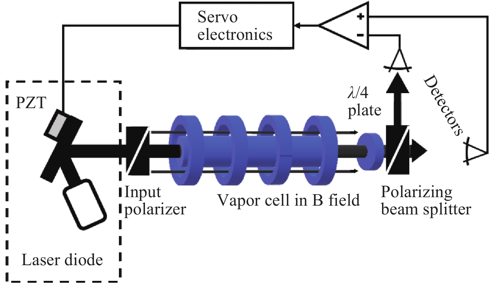
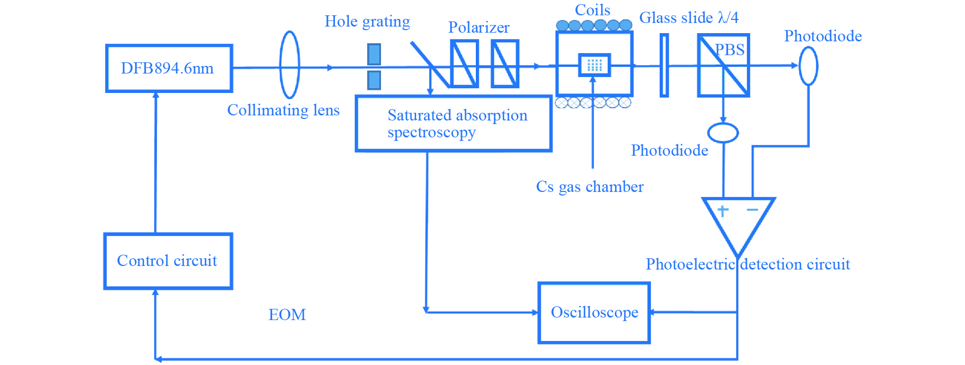
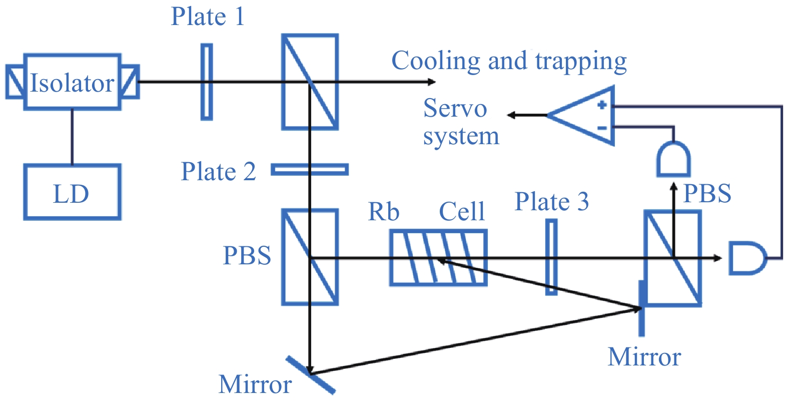
The frequency stability of free-running semiconductor lasers is influenced by several factors, such as driving current and external operating environment. The frequency stabilization of laser has become an international research hotspot in recent years. This paper reviews active frequency stabilization technologies of laser diodes and elaborates their principles. Based on differences of frequency discrimination curves, these active frequency stabilization technologies are classified into three major types, which are harmonic frequency stabilization, Pound-Drever-Hall (PDH) technology and curve subtraction frequency stabilization. Further, merits and demerits of each technology are compared from aspects of frequency stability and structure complexity. Finally, prospects of frequency stabilization technologies of semiconductor lasers are discussed in detail. Combining several of these methods are future trends, especially the combination of frequency stabilization of F–P cavity. And PID electronic control for optimizing the servo system is generally added in the methods mentioned above.


J. Semicond.
2018, 39(11): 114005 doi: 10.1088/1674-4926/39/11/114005
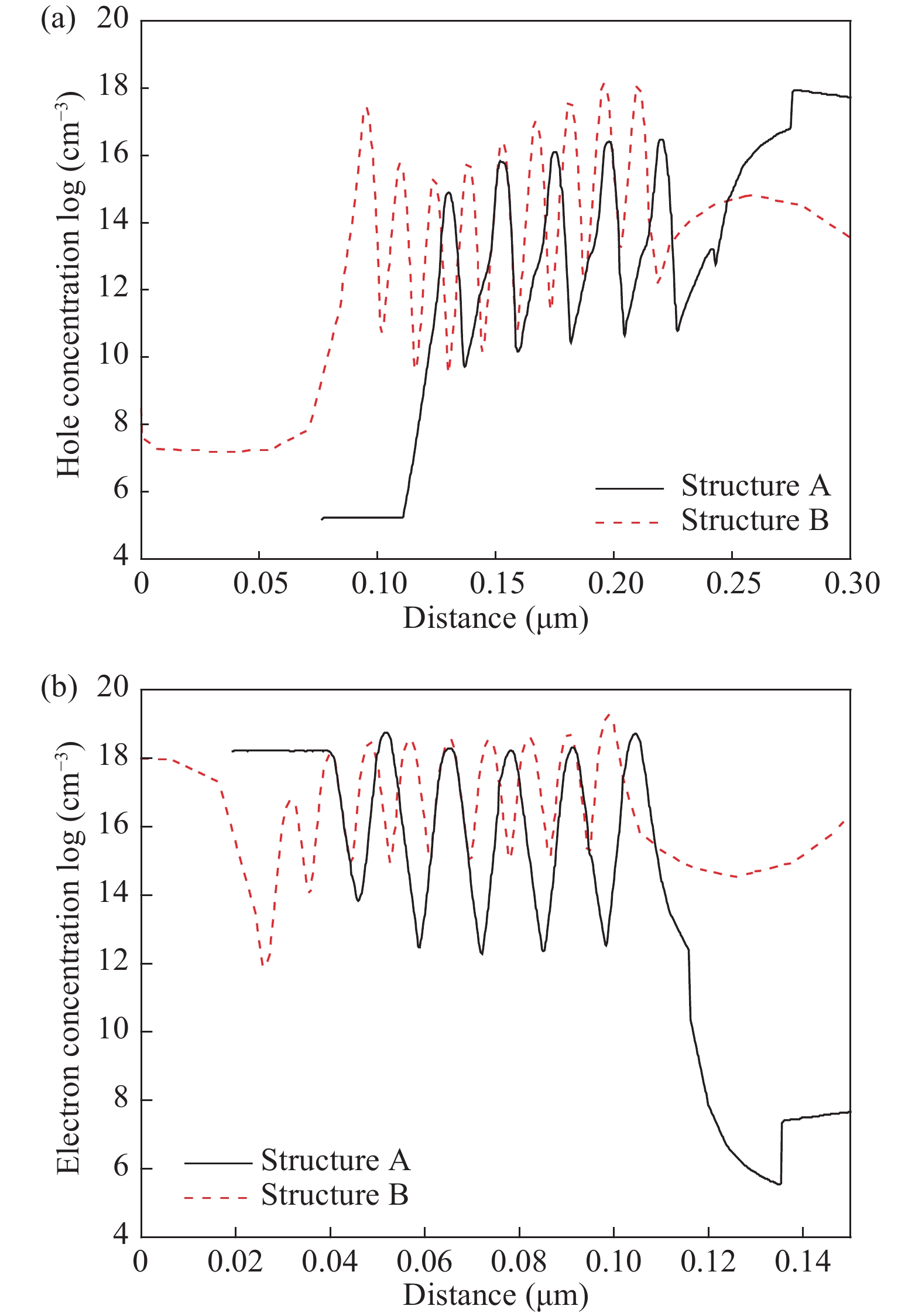
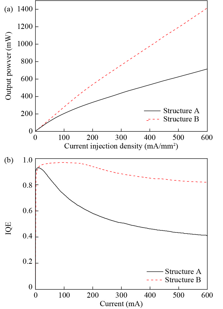
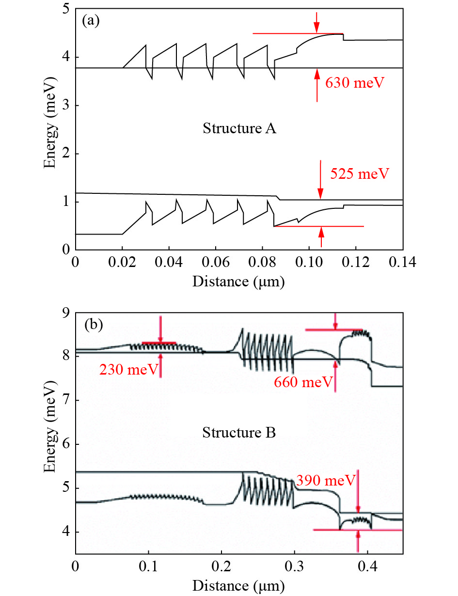
In this study, the effect of double superlattices on GaN-based blue light-emitting diodes (LEDs) is analyzed numerically. One of the superlattices is composed of InGaN/GaN, which is designed before the multiple quantum wells (MQWs). The other one is AlInGaN/AlGaN, which is inserted between the last QB (quantum barriers) and p-GaN. The crucial characteristics of double superlattices LEDs structure, including the energy band diagrams, carrier concentrations in the active region, light output power, internal quantum efficiency, respectively, were analyzed in detail. The simulation results suggest that compared with the conventional AlGaN electron-blocking layer (EBL) LED, the LED with double superlattices has better performance due to the enhancement of electron confinement and the increase of hole injection. The double superlattices can make it easier for the carriers tunneling to the MQWs, especially for the holes. Furthermore, the LED with the double superlattices can effectively suppress the electron overflow out of multiple quantum wells simultaneously. From the result, we argue that output power is enhanced dramatically, and the efficiency droop is substantially mitigated when the double superlattices are used.
J. Semicond.
2018, 39(11): 114006 doi: 10.1088/1674-4926/39/11/114006
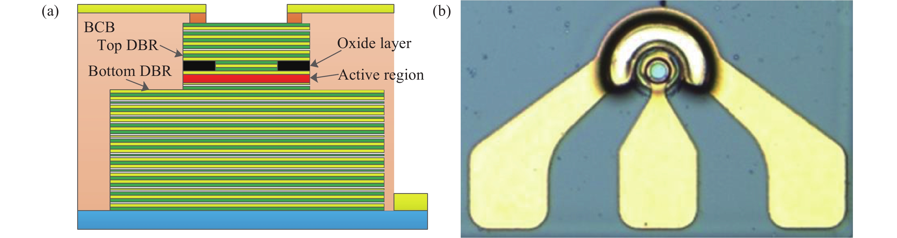
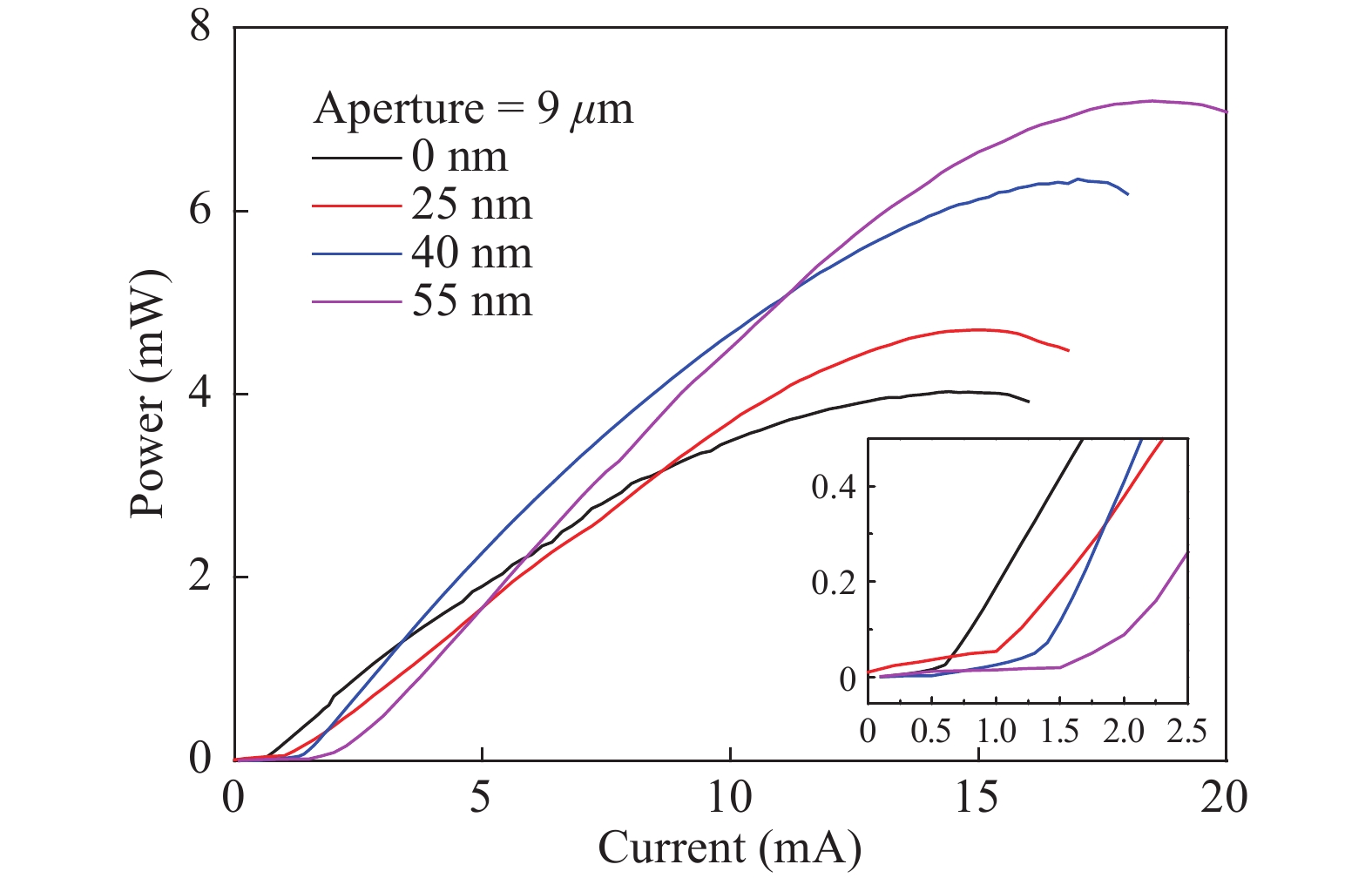
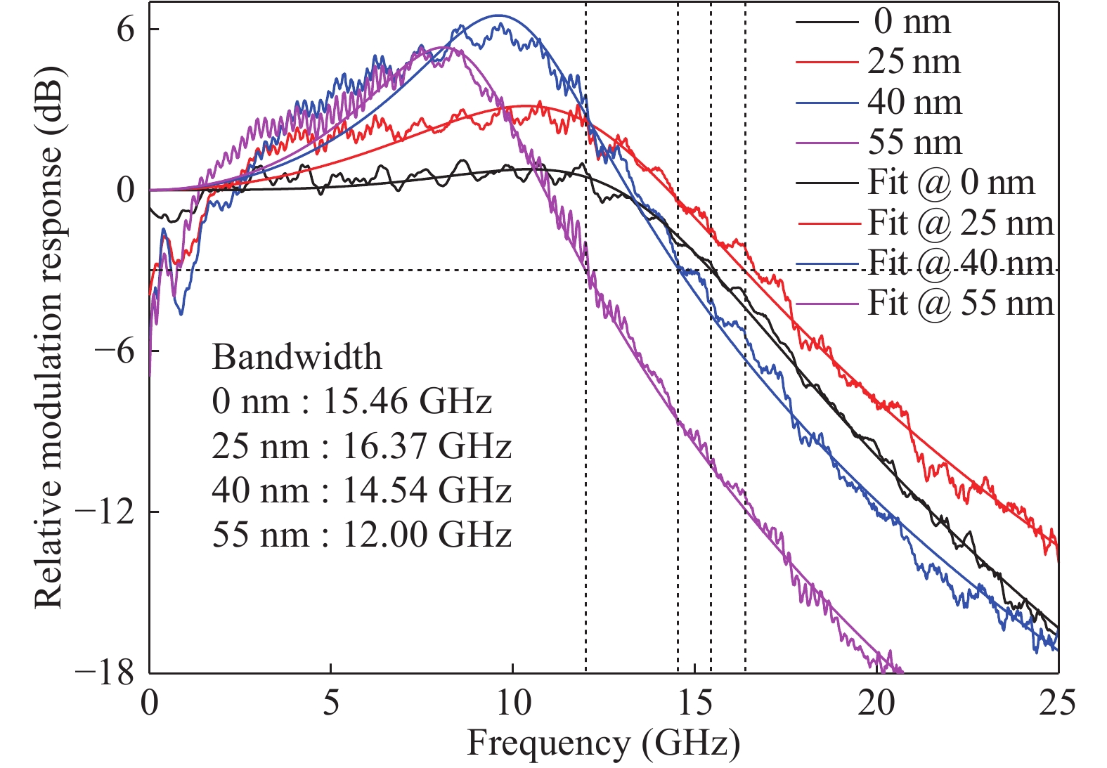
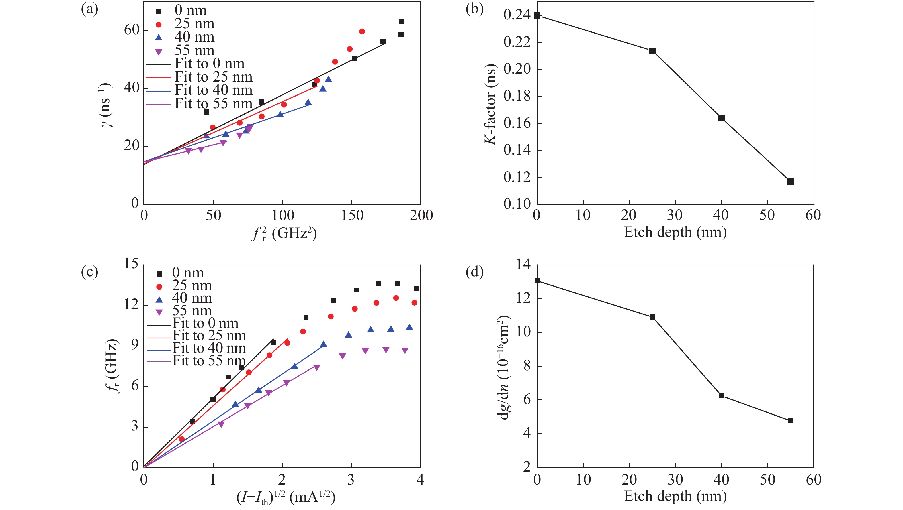
High speed VCSELs are important optical devices in short-reach optical communication links and interconnects because of their low cost and high modulation speeds. In this paper, the impact of damping on the their static and dynamic characteristics is analyzed and demonstrated. Through the shallow corrosion of the top layer DBR, the VCSELs with different damping is designed and fabricated. With the increase of the surface etch depth from 0 to ~55 nm for 9 μm oxide-aperture VCSEL, the K factor related with the damping is reduced from 0.31 to 0.23 ns−1. When the etch depth of the VCSEL with 9 μm oxide-aperture is decreased to ~25 nm, output power is increased from 4.03 to 4.70 mW and small signal modulation bandwidth is also increased from 15.46 to 16.37 GHz. It shows that there is a tradeoff between damping and differential gain for improving modulation speed.

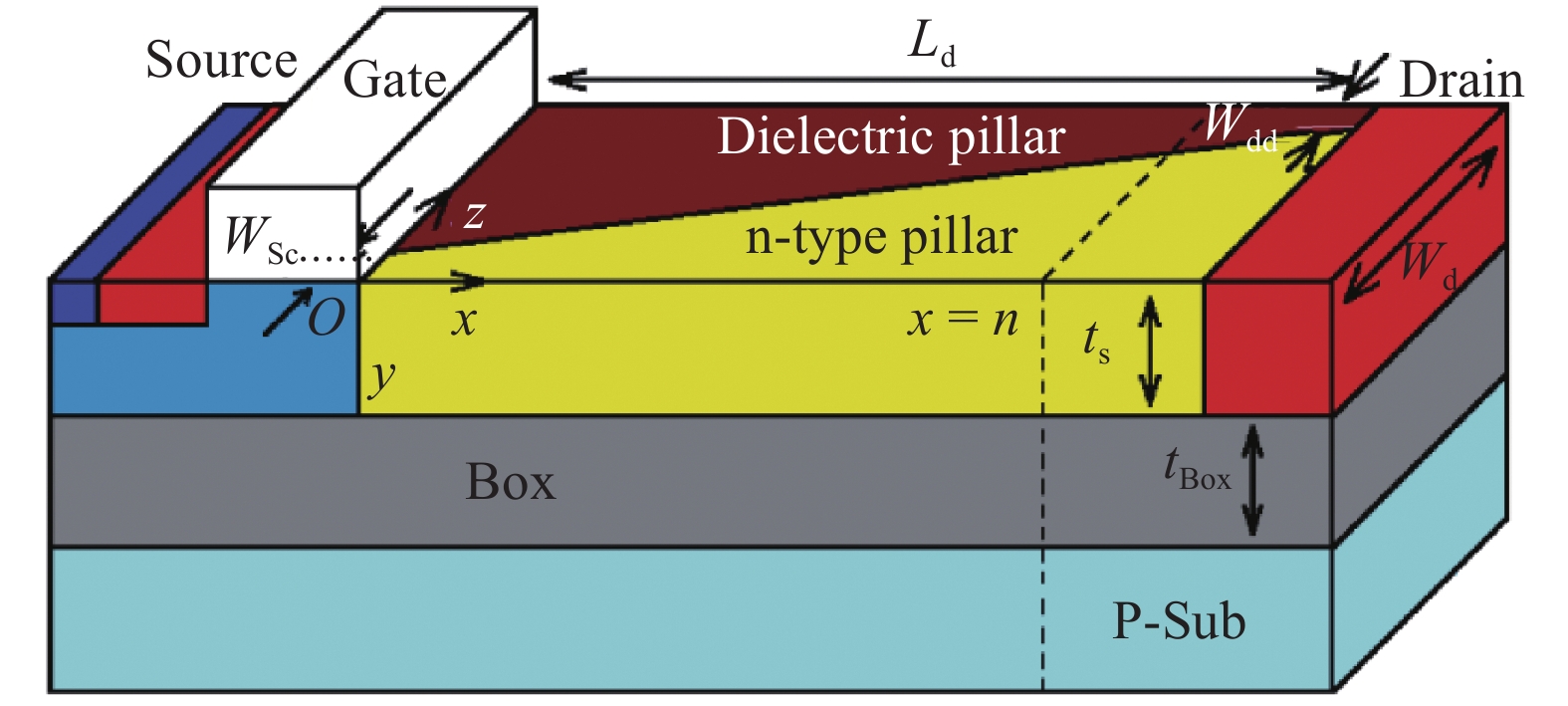
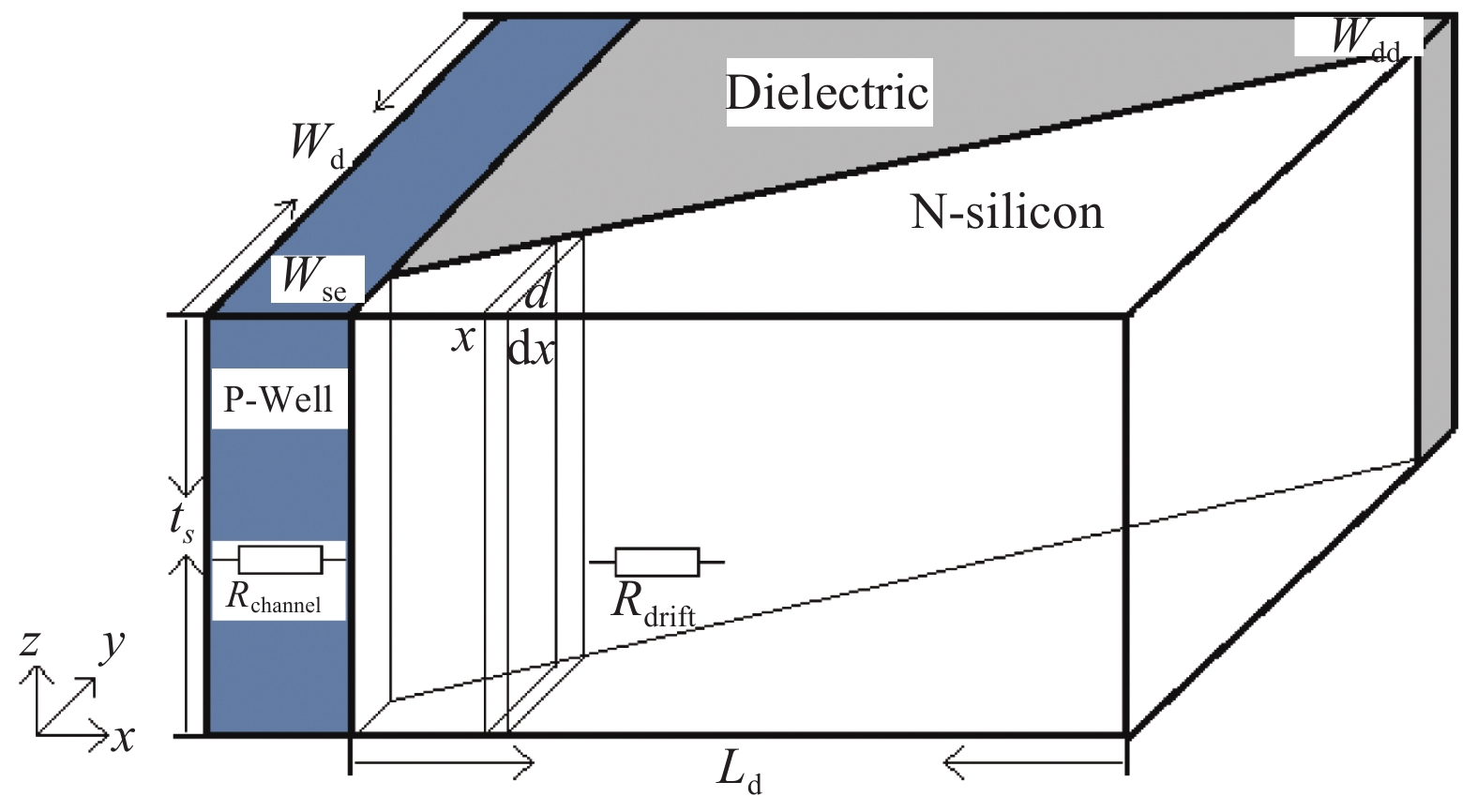
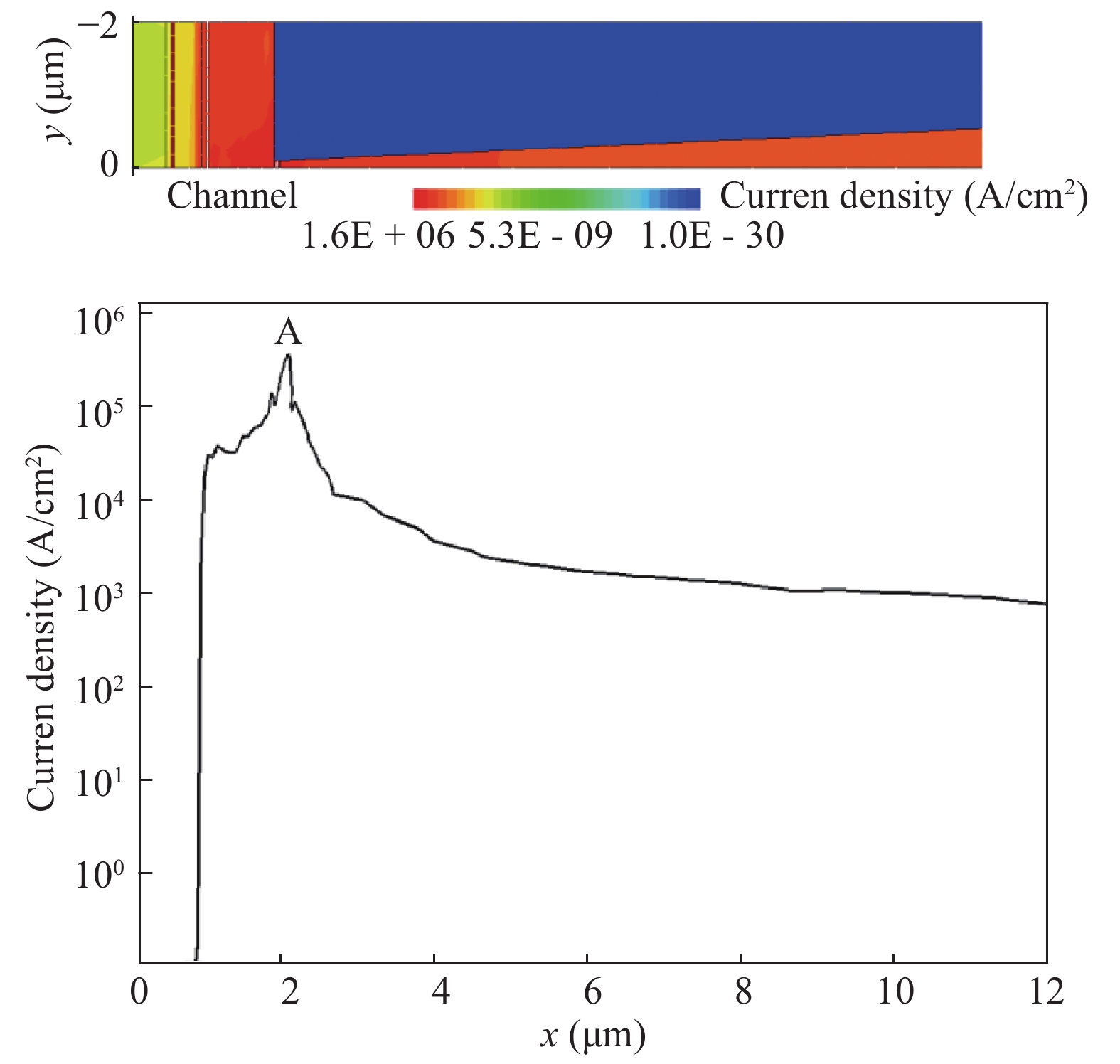
Investigation of the on-state behaviors of the variation of lateral width LDMOS device by simulation
J. Semicond.
2018, 39(11): 114007 doi: 10.1088/1674-4926/39/11/114007
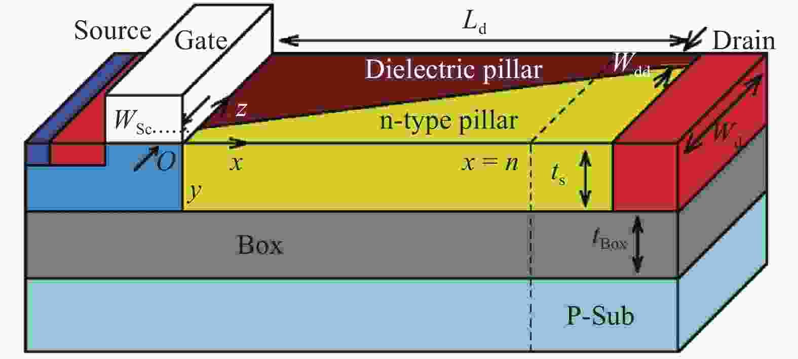
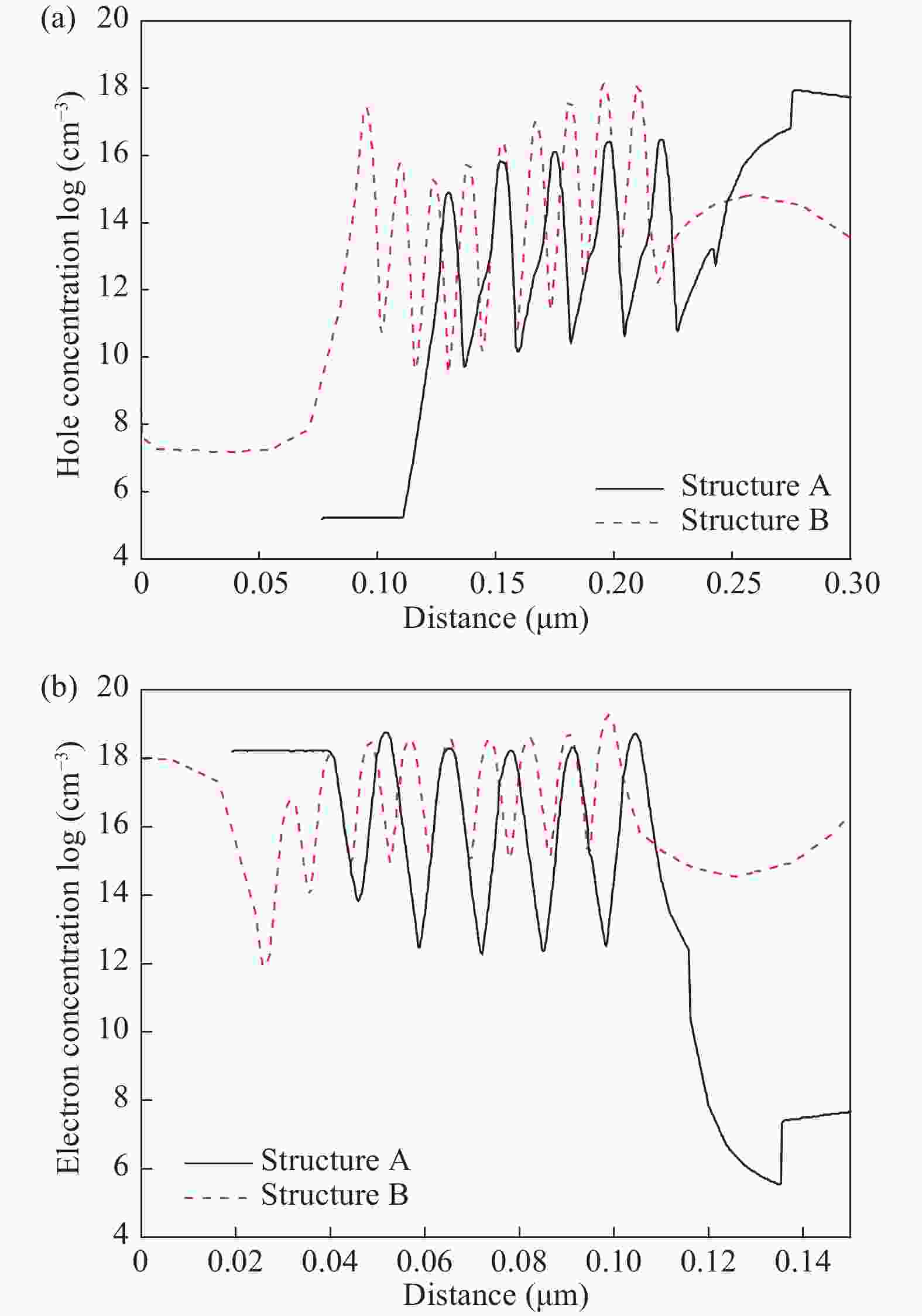
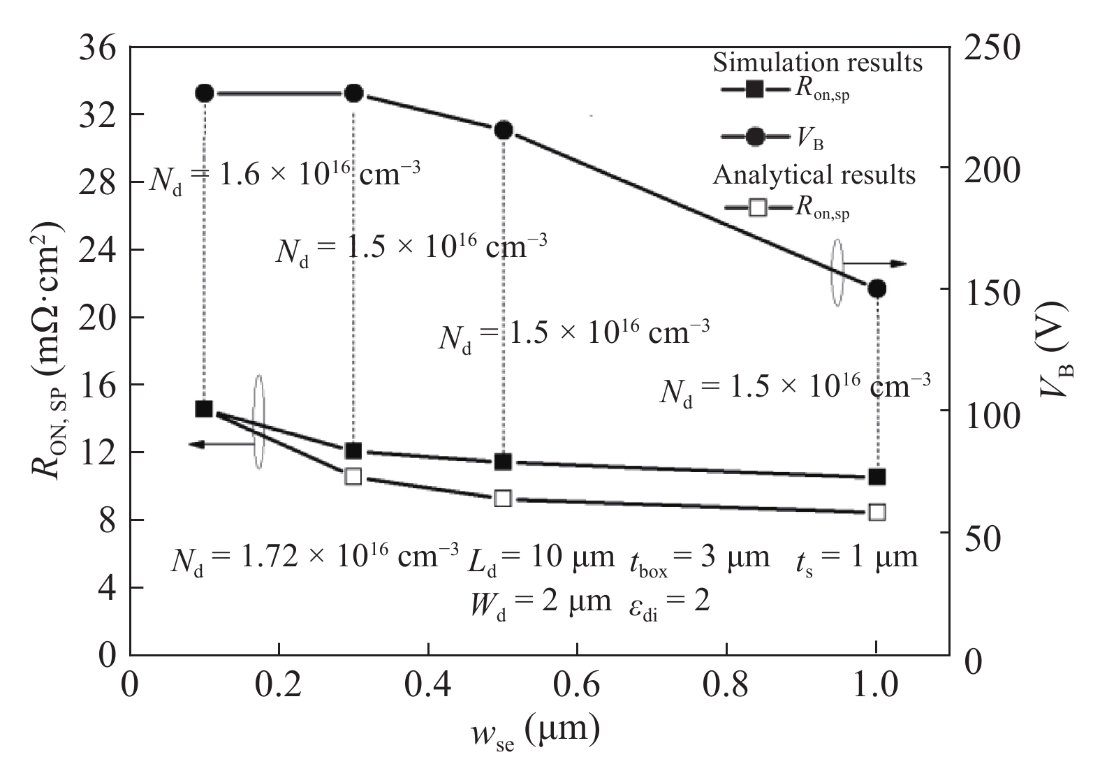
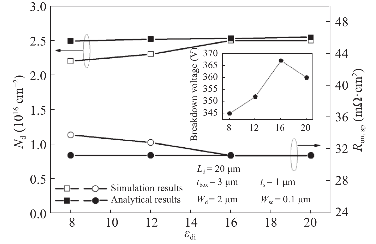
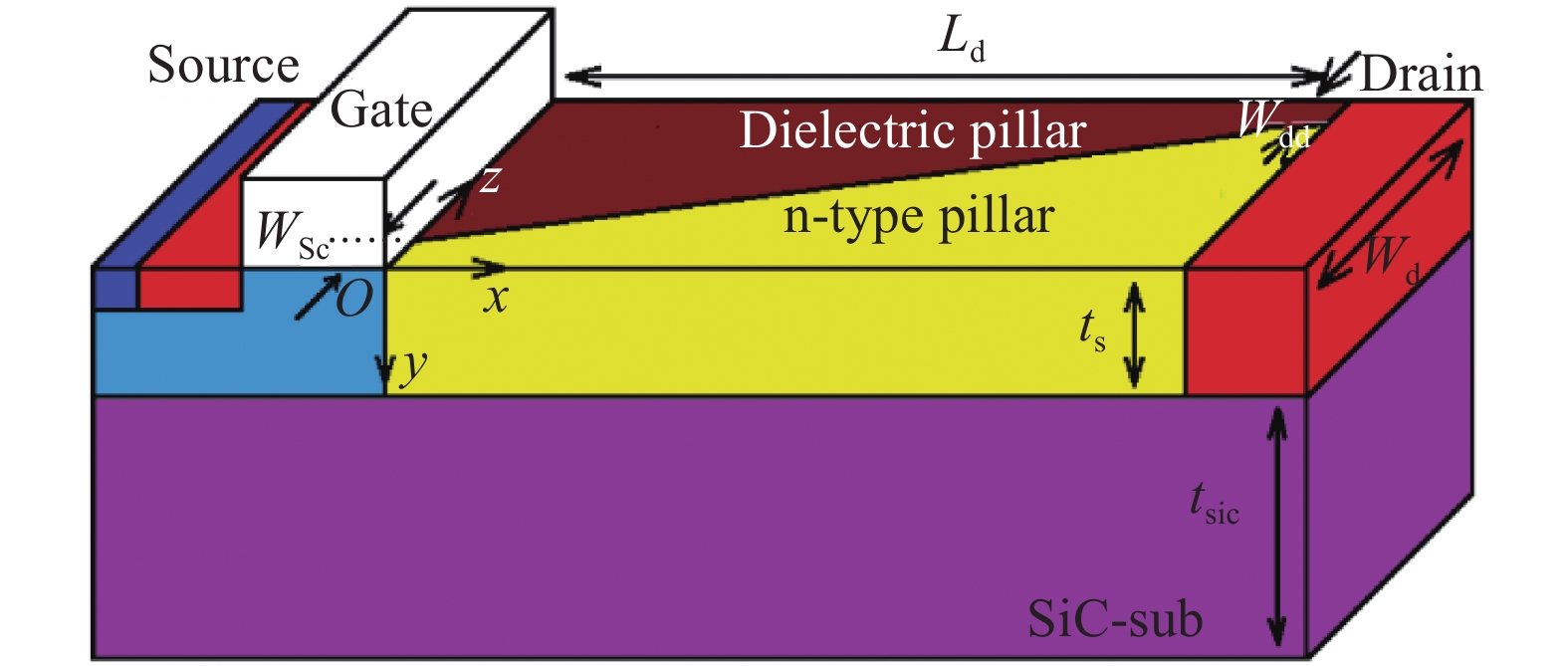
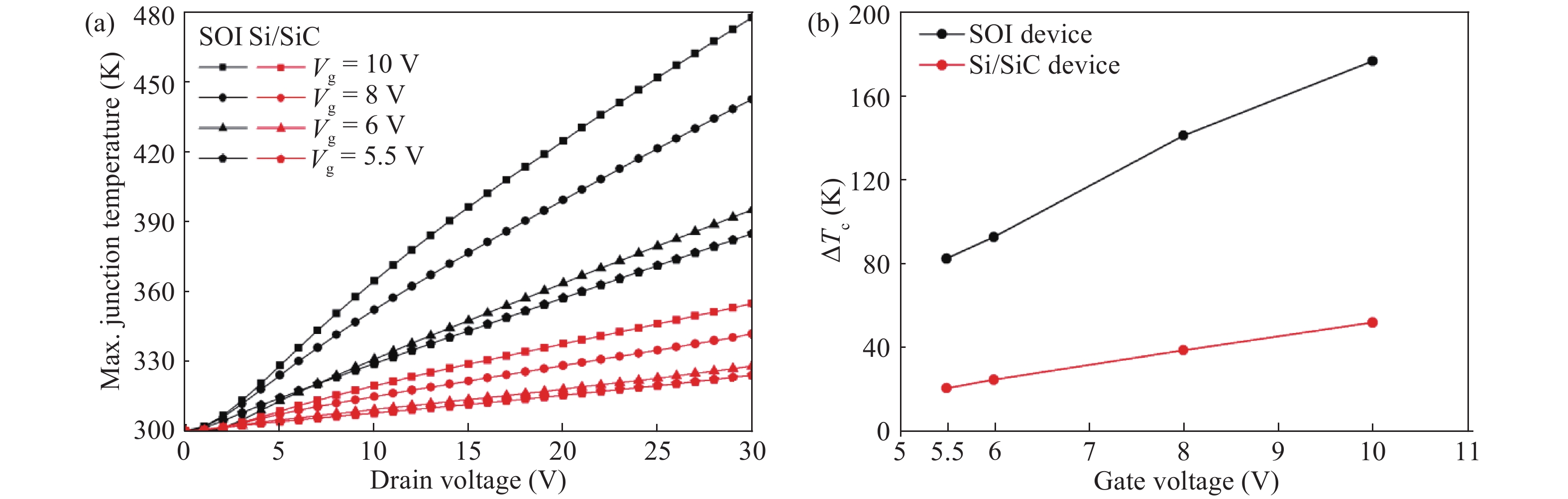
The main content revolves round the on-state characteristics of the variation of a lateral width (VLW) LDMOS device. A three-dimensional numerical analysis is performed to investigate the specific on-resistance of the VLW LDMOS device, the simulation results are in good agreement with the analytical calculation results combined with device dimensions. This provides a theoretical basis for the design of devices in the future. Then the self-heating effect of the VLW structure with a silicon-on-oxide (SOI) substrate is compared with that of a silicon carbide (SiC) substrate by 3D thermoelectric simulation. The electrical characteristic and temperature distribution indicate that taking into account the SiC as the substrate can mitigate the self- heating penalty effectively, alleviating the self heating effect and improving reliability.


J. Semicond.
2018, 39(11): 114008 doi: 10.1088/1674-4926/39/11/114008
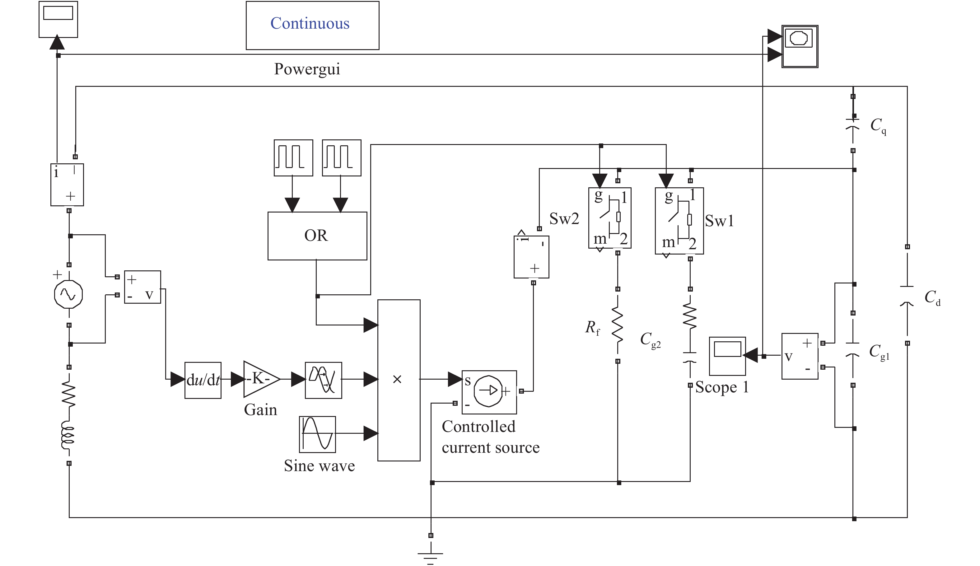
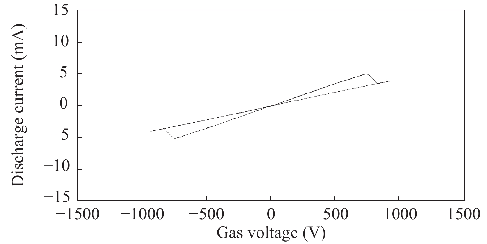
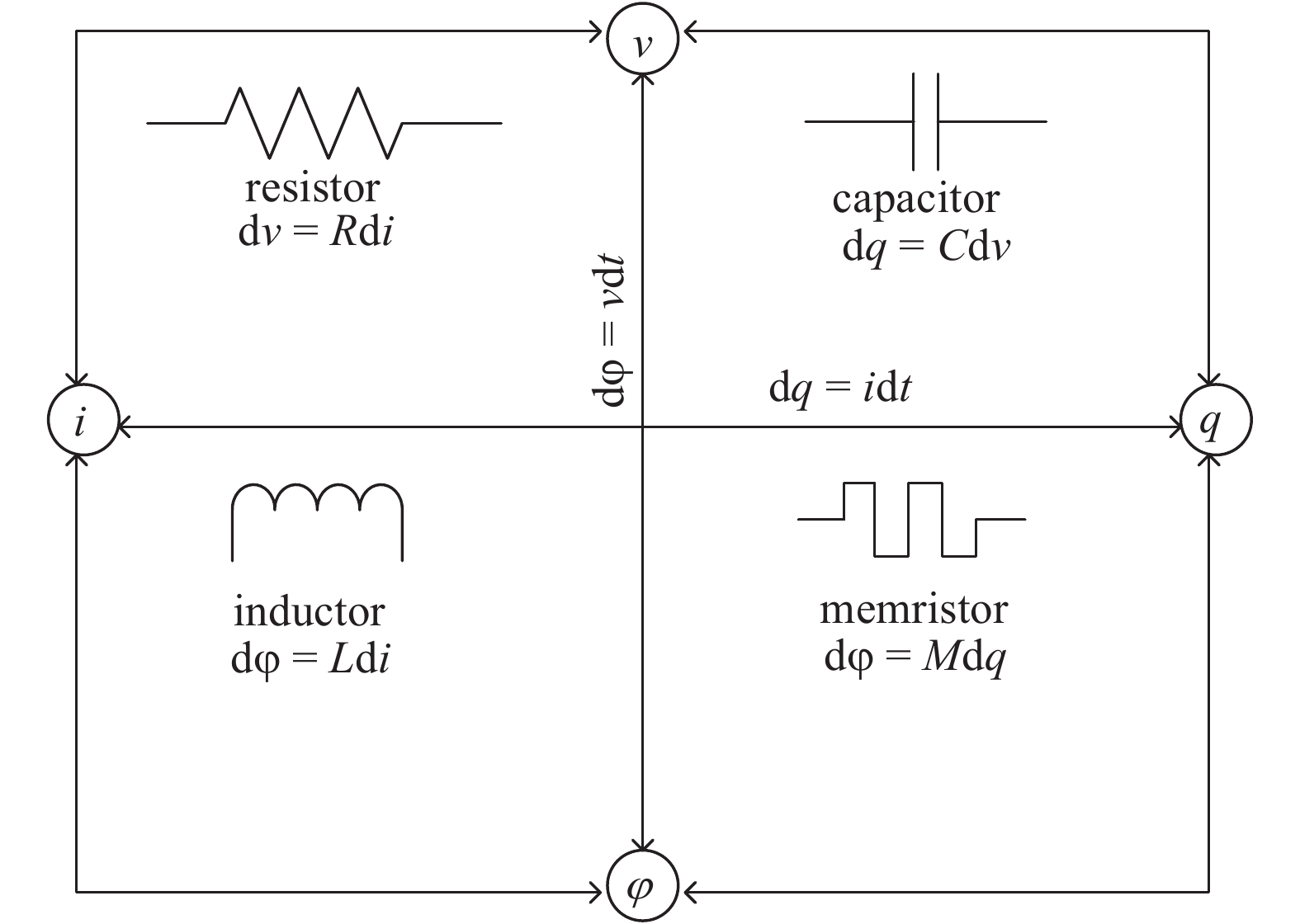
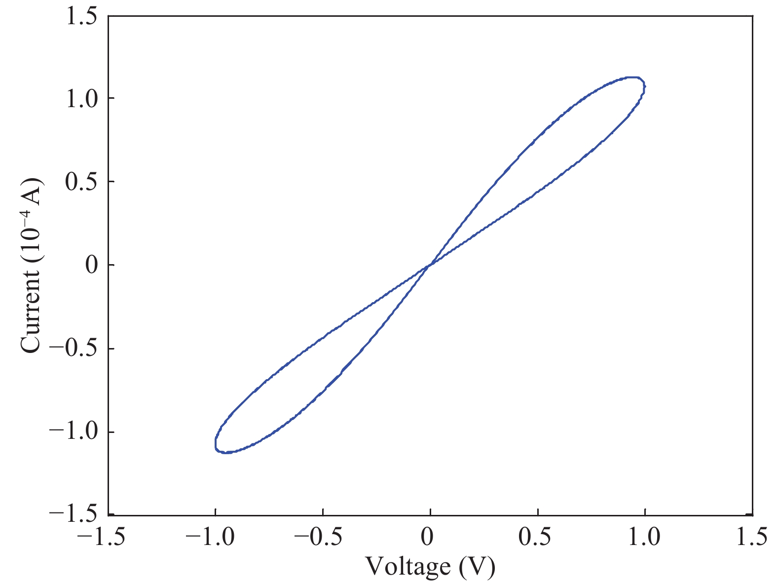
The nonlinear resistance characteristics of microcavity dielectric barrier discharge are mainly studied in the paper. A simulation model of microcavity dielectric barrier discharge is herein built to study the relationship between voltage and current in the process of discharge, and thus its I–V characteristic curve can be obtained. The I–V characteristics of the memristor are analyzed and compared with the I–V characteristics of the dielectric barrier discharge; it can be found that the I–V characteristics of the microcavity dielectric barrier discharge are similar to the characteristics of the memristor by analyzing them. The memory characteristics of microcavity dielectric barrier discharge are further analyzed.

J. Semicond.
2018, 39(11): 115001 doi: 10.1088/1674-4926/39/11/115001
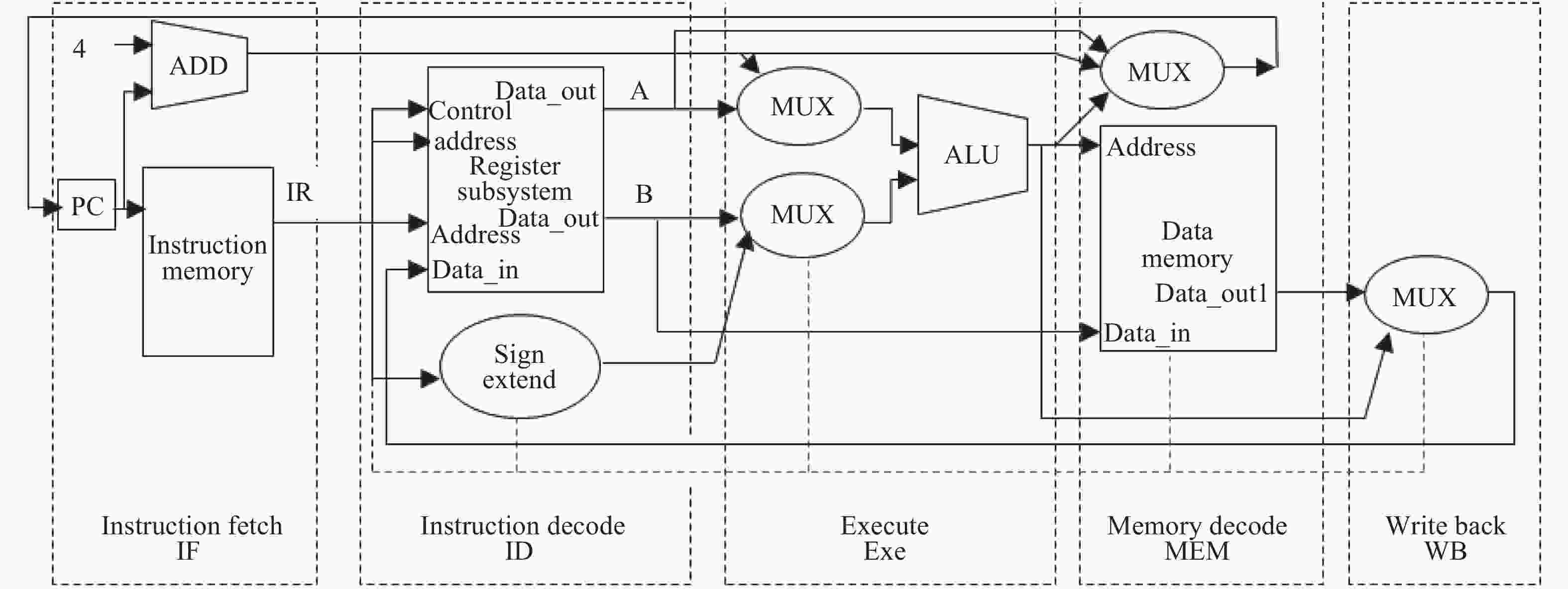
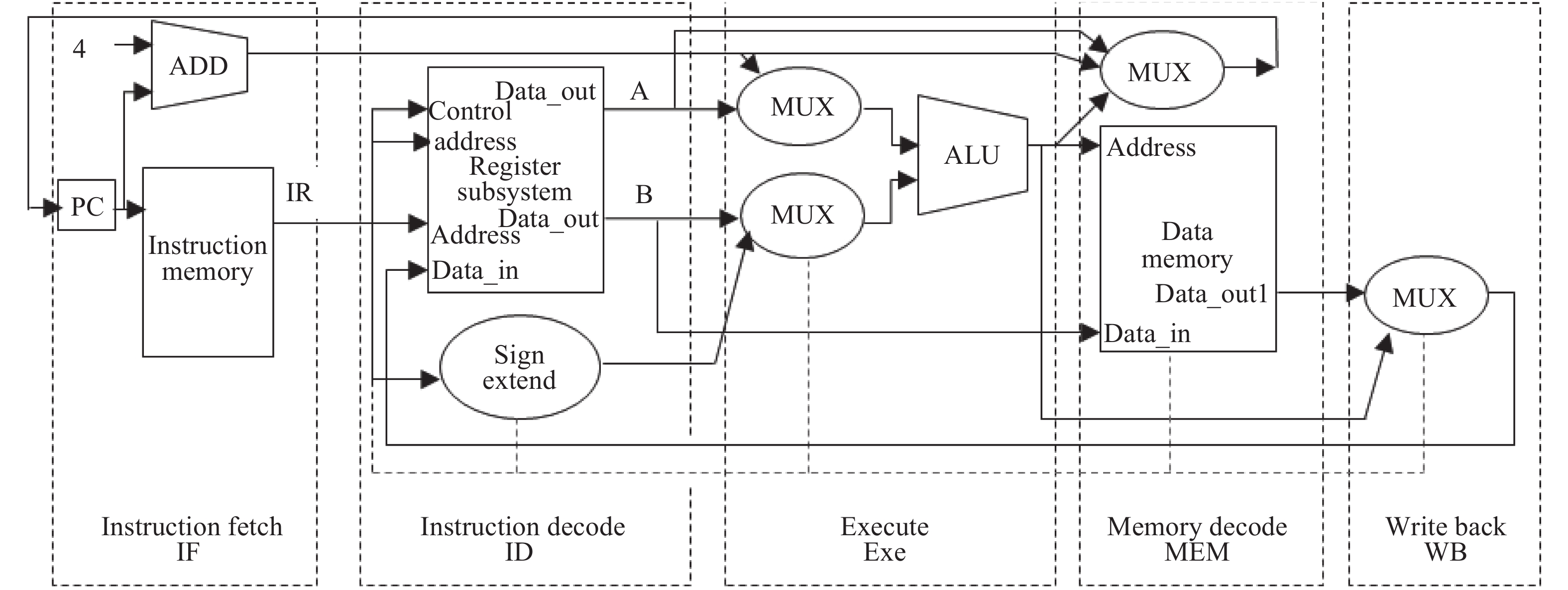
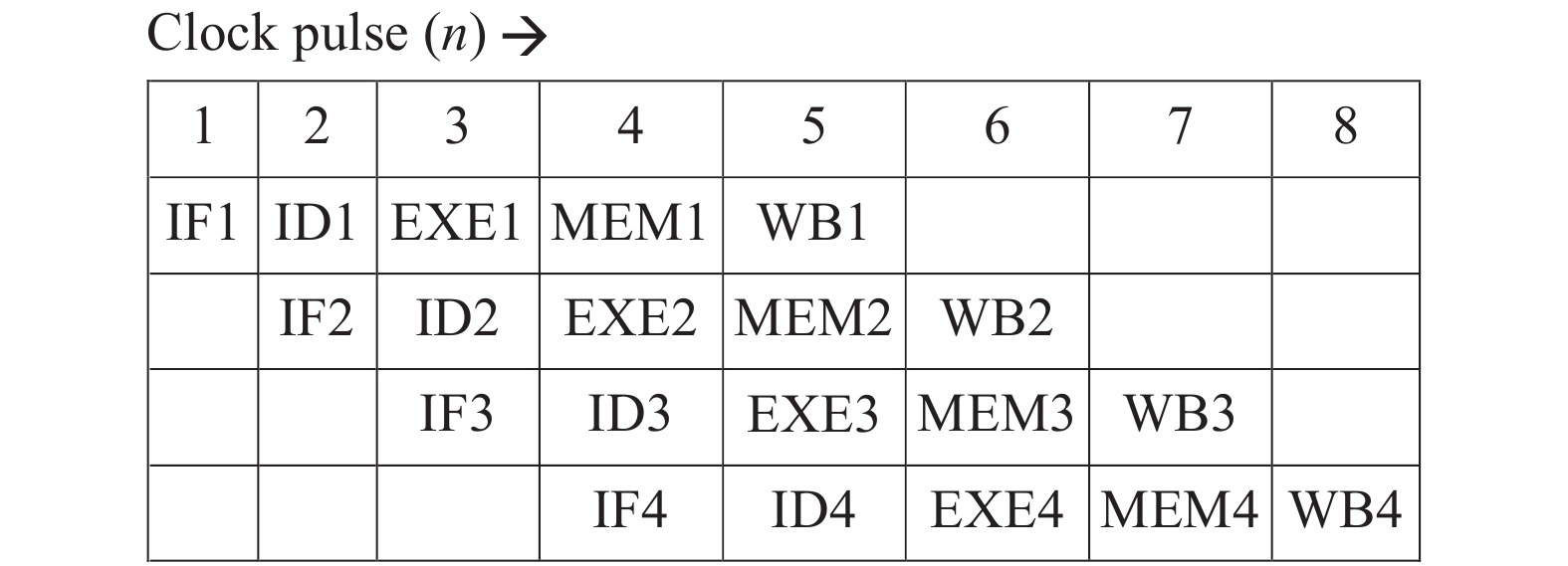
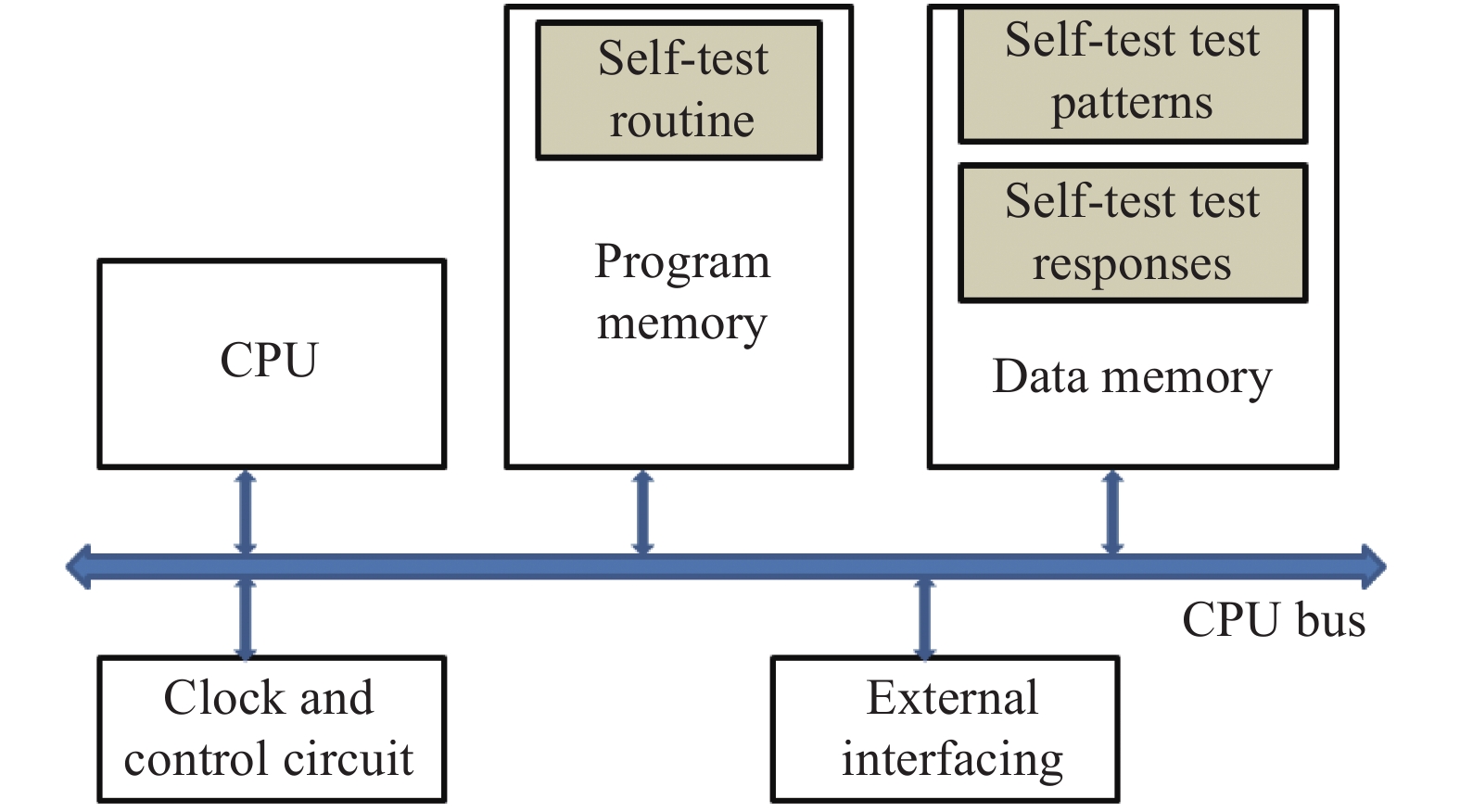
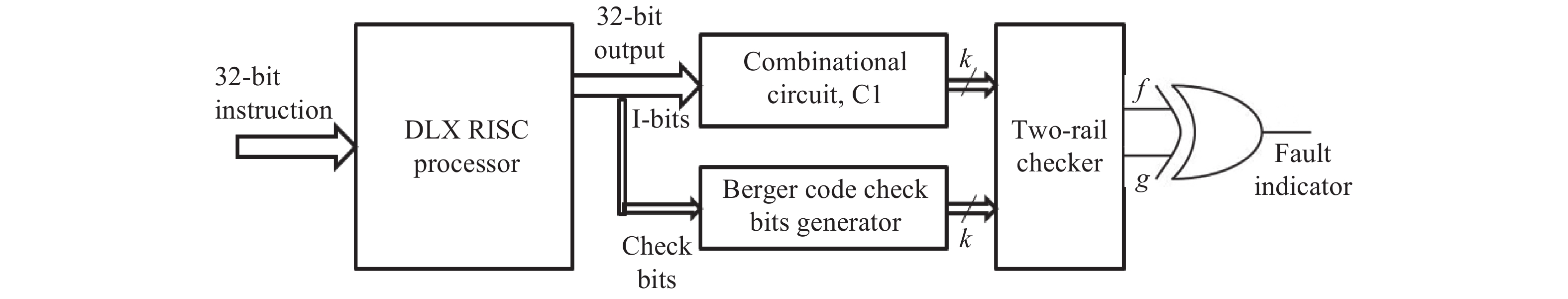
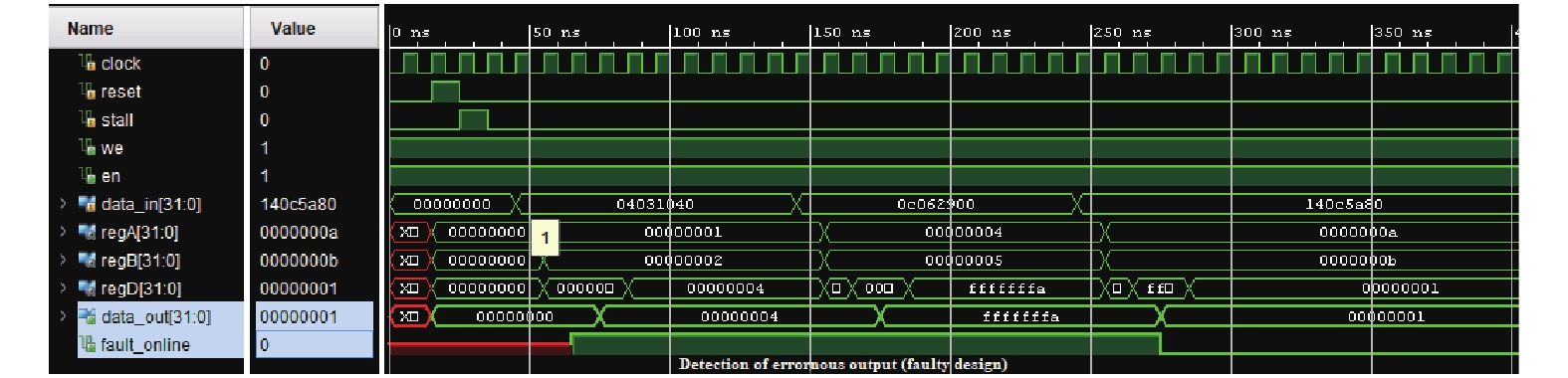
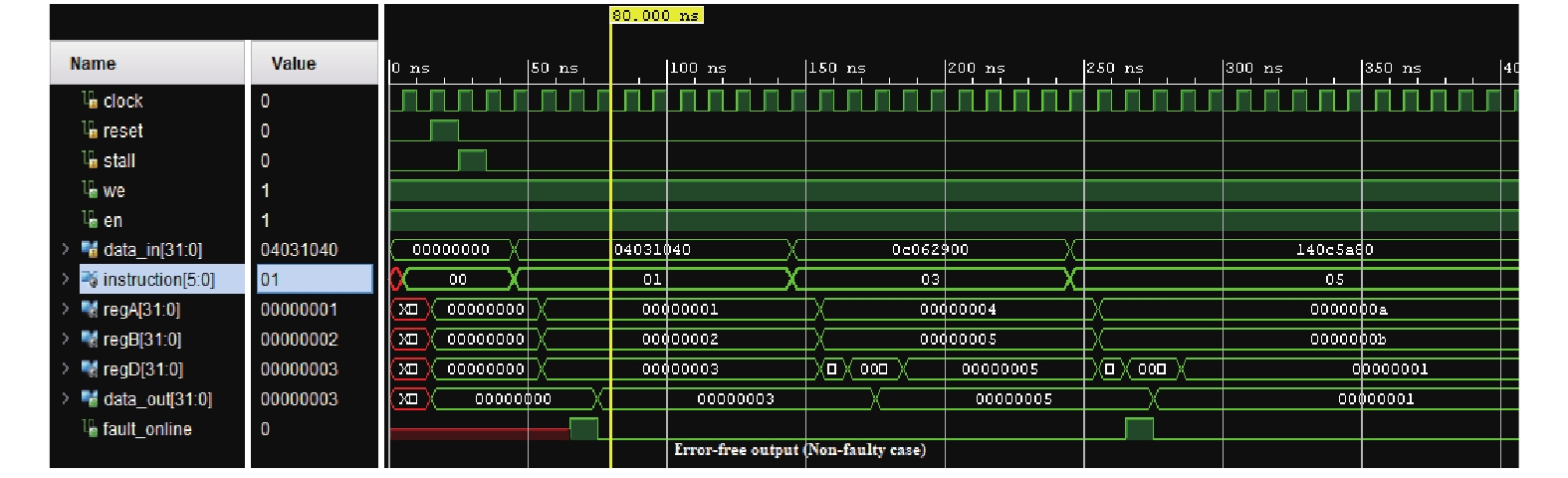
We propose an approach to detect the temporary faults induced by an environmental phenomenon called single event upset (SEU). Berger code based self-checking checkers provides an online detection of faults in digital circuits as well as in memory arrays. In this work, a concurrent Berger code based online self- testable architecture is proposed and integrated in 32-bit DLX reduced instruction set computer (RISC) processor on a single silicon chip. The proposed concurrent test methodology is implemented and verified for various arithmetic and logical operations of the DLX processor. The FPGA implementation of the proposed design shows that a meager increase in hardware utilization facilitates online self-testing to detect temporary faults.

J. Semicond.
2018, 39(11): 115002 doi: 10.1088/1674-4926/39/11/115002

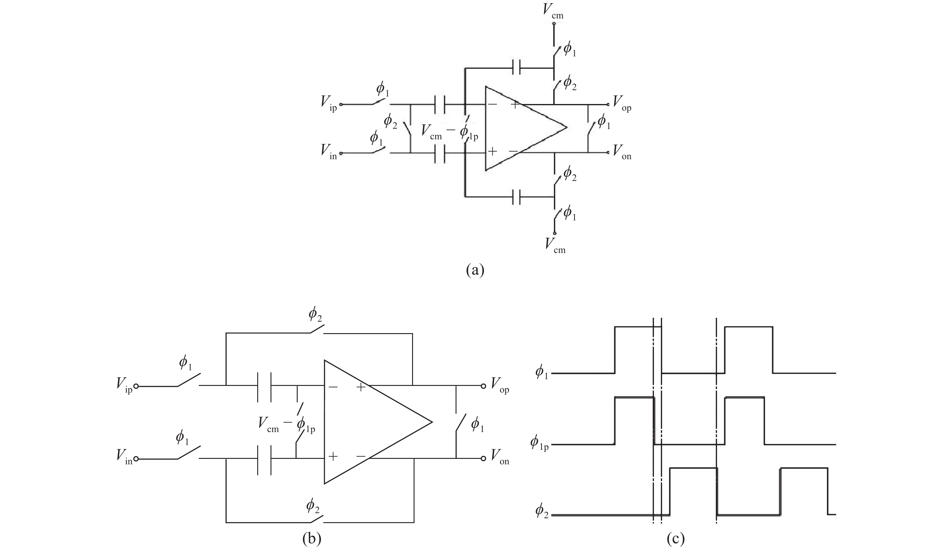
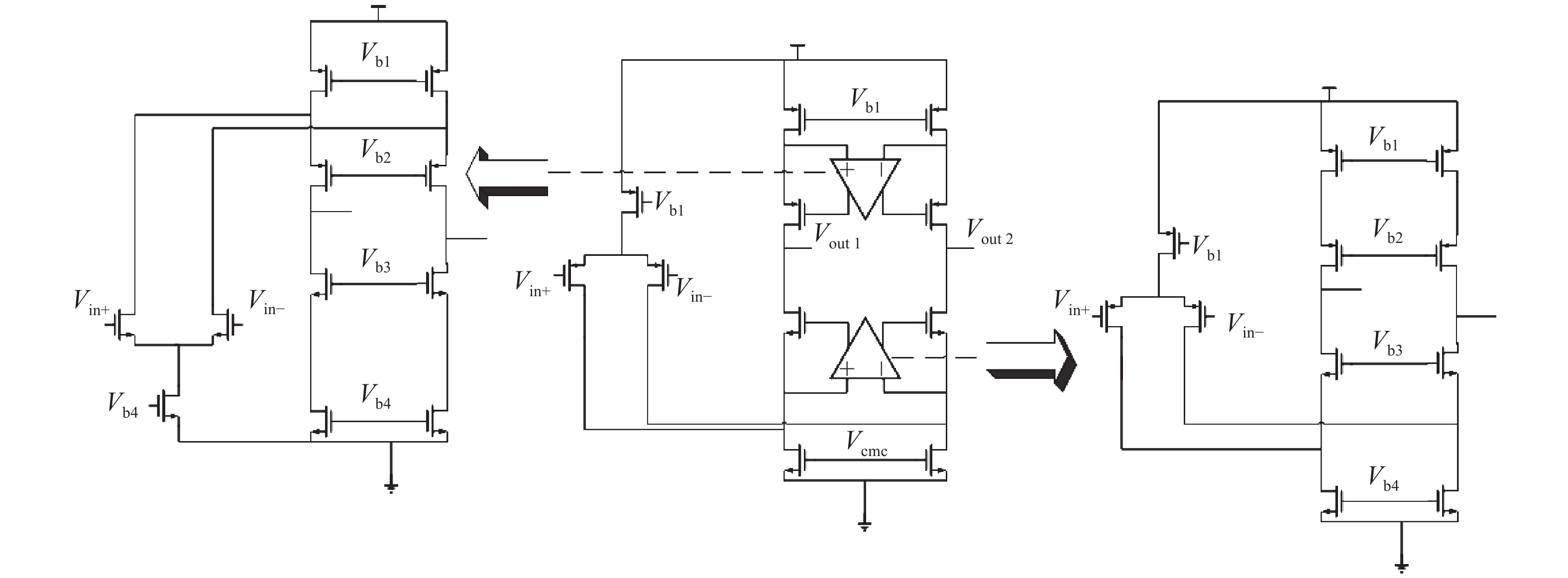
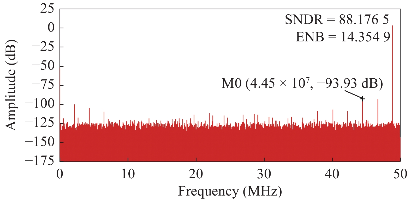
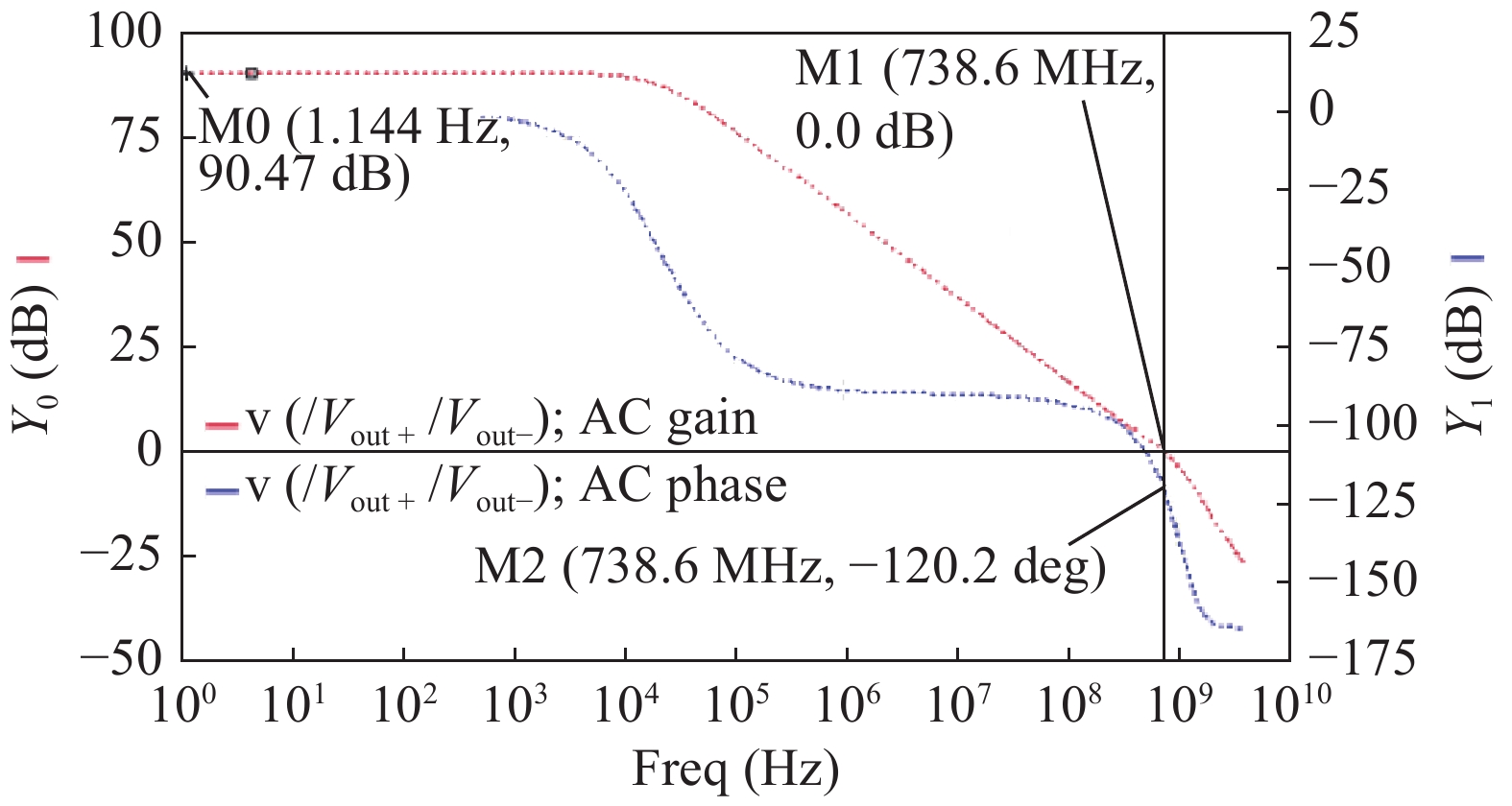
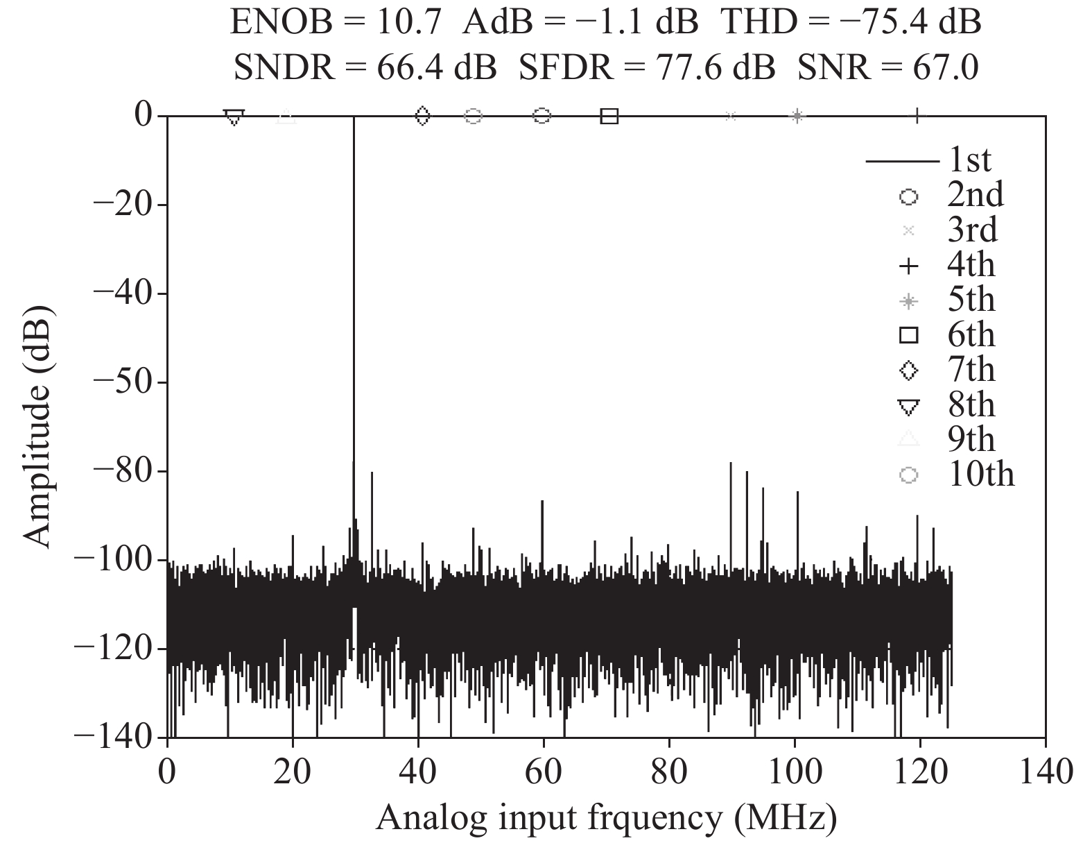
A high performance sample-and-hold (S/H) circuit used in a pipelined analog-to-digital converter (ADC) is presented in this paper. Fully-differential capacitor flip-around architecture was used in this S/H circuit. A gain-boosted folded cascode operational transconductance amplifier (OTA) with a DC gain of 90 dB and a GBW of 738 MHz was designed. A low supply voltage bootstrapped switch was used to improve the linearity of the S/H circuit. With these techniques, the designed S/H circuit can reach 94 dB SFDR for a 48.9 MHz input frequency with 100 MS/s sampling rate. Measurement results of a 14-bit 100-MS/s pipeline ADC with designed S/H circuit are presented.


J. Semicond.
2018, 39(11): 115003 doi: 10.1088/1674-4926/39/11/115003

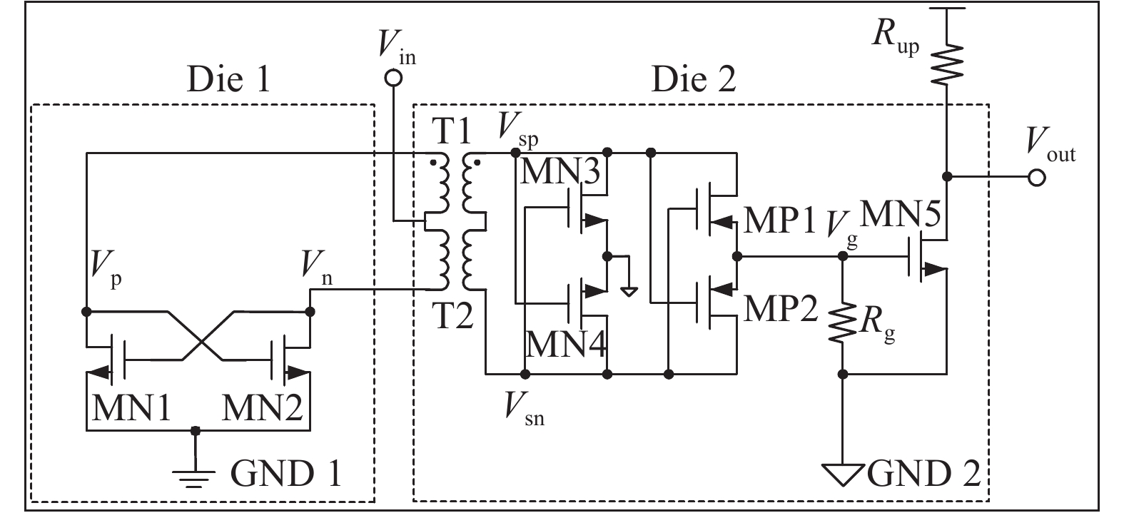
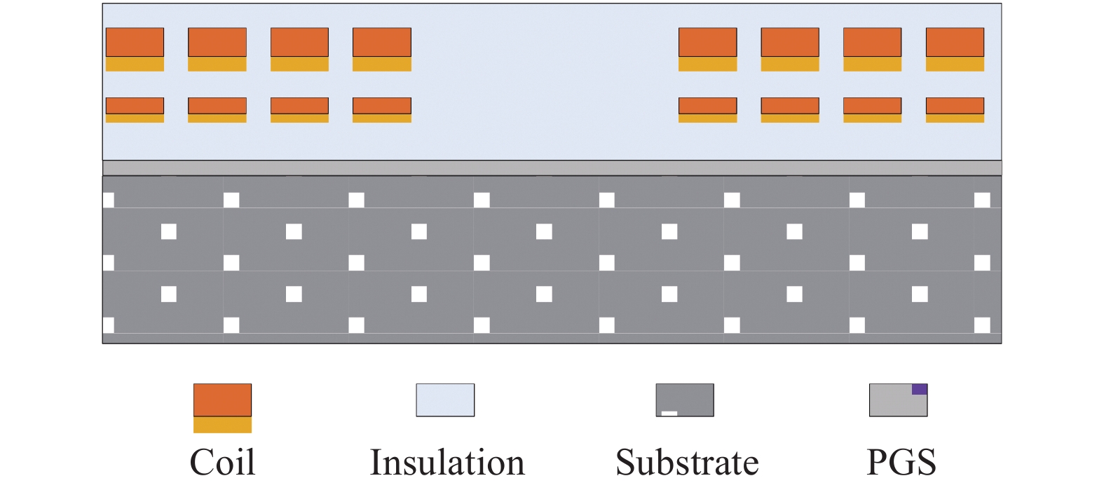
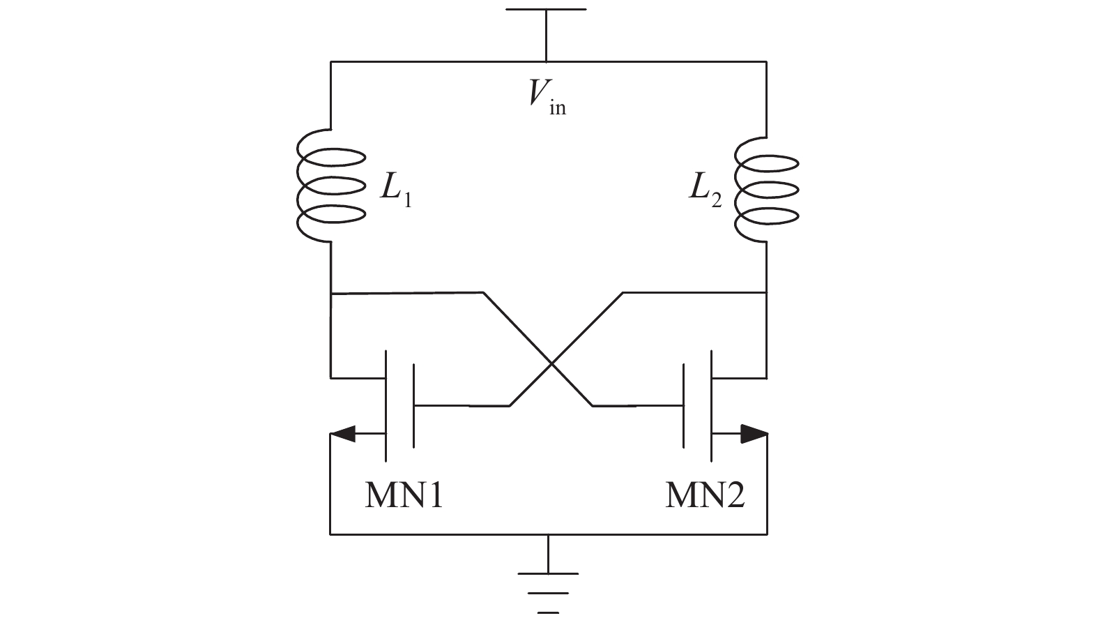
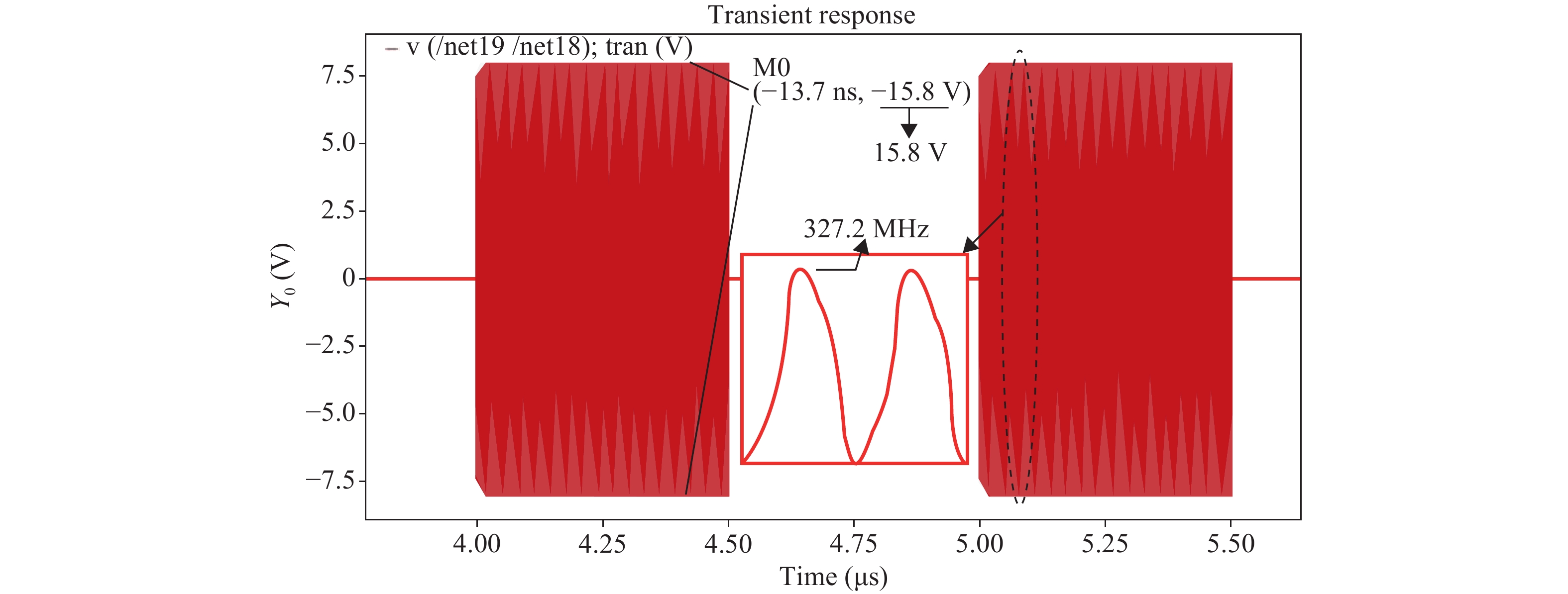
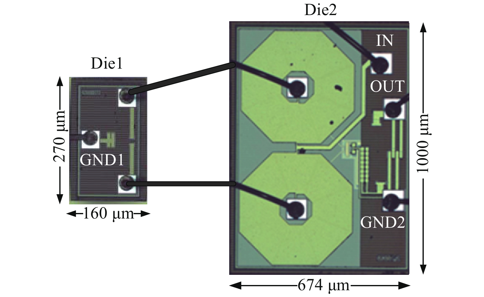
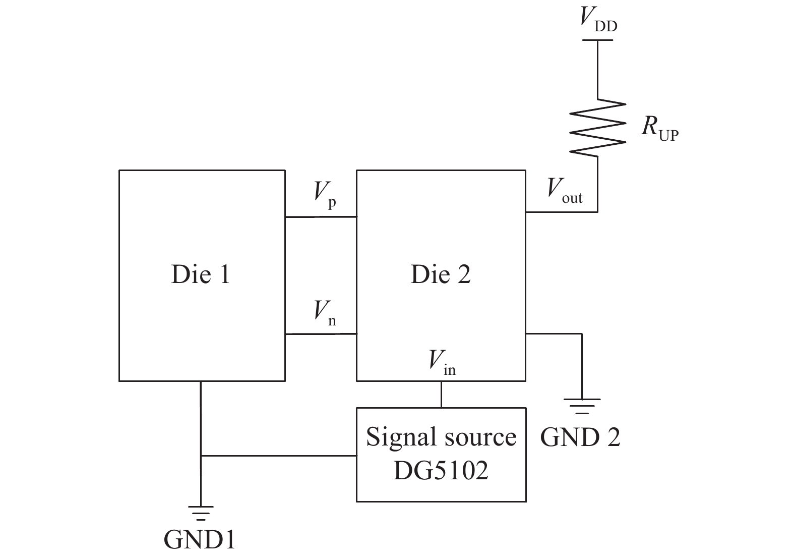
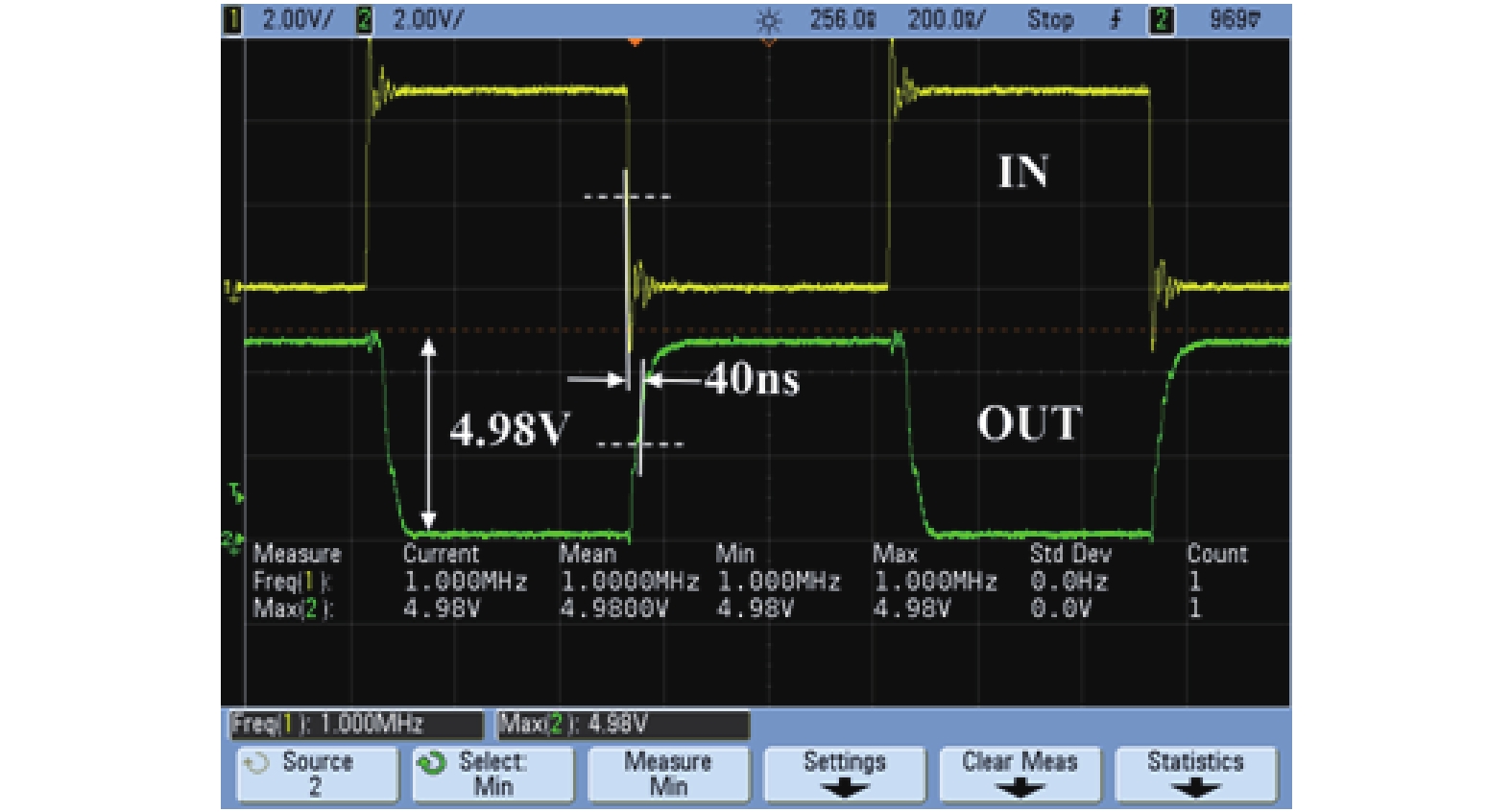
The design and fabrication results of a 4-port digital isolator based on an on-chip transformer for galvanic isolation are presented. An ON–OFF keying modulation scheme is used to transmit the digital signal. The proposed digital isolator is fabricated by the 0.18 μm CMOS process. A test chip can achieve a 1 MHz signal bandwidth, a 40 ns propagation delay, a 35.5 mW input power and a 50 mA drive output current. The proposed digital isolator is pin-compatible, of small volume and low power replacement for the common 4-port optocoupler.