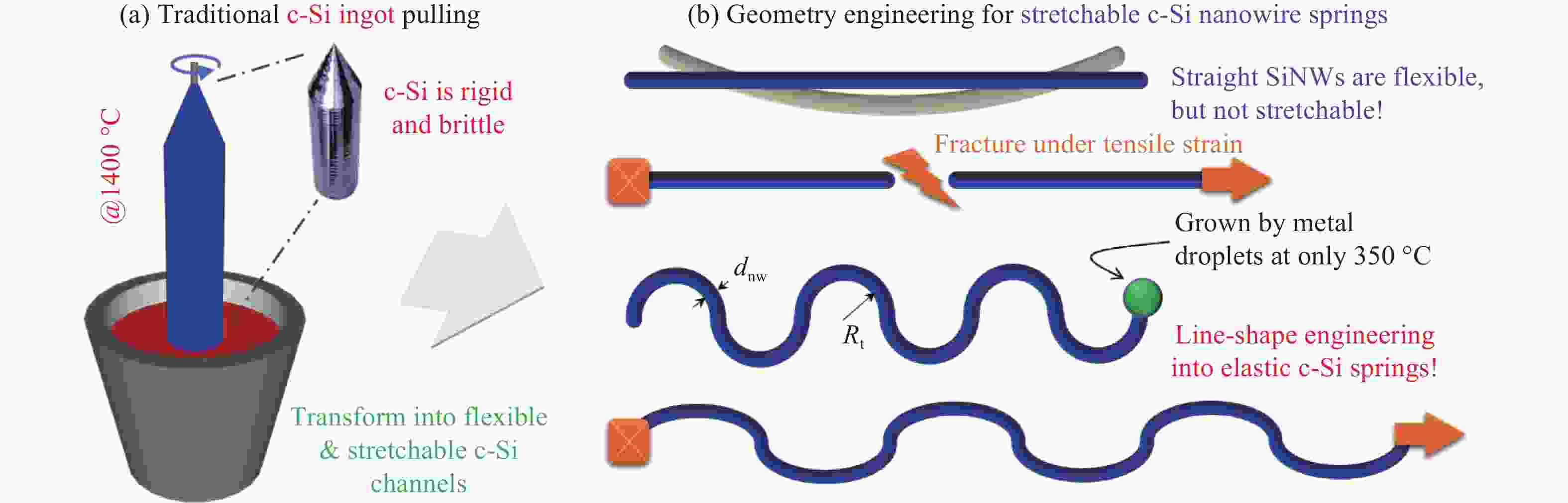
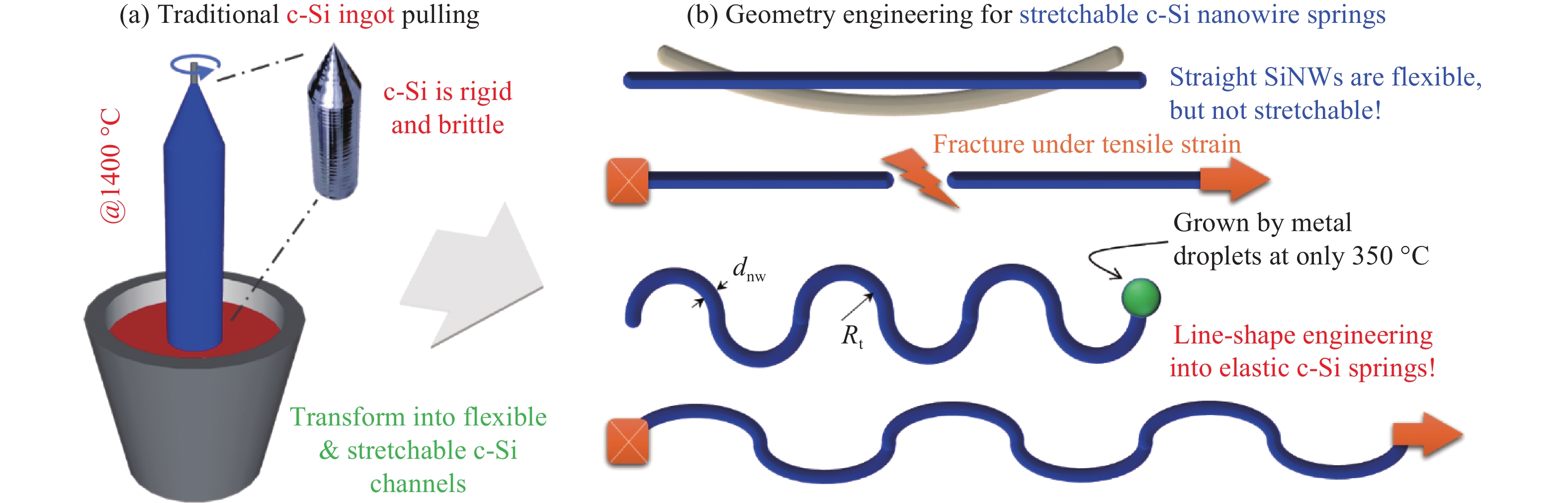
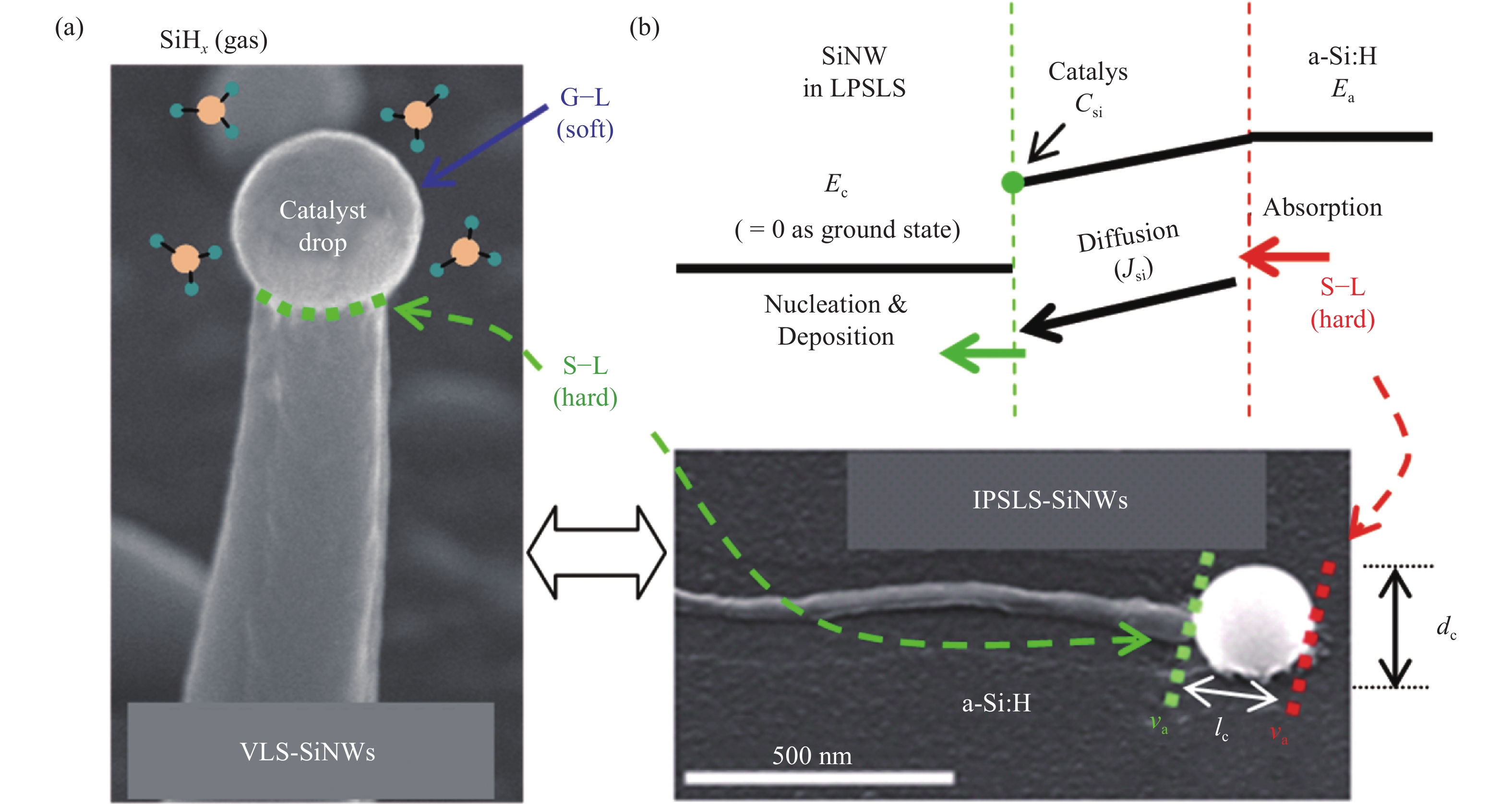
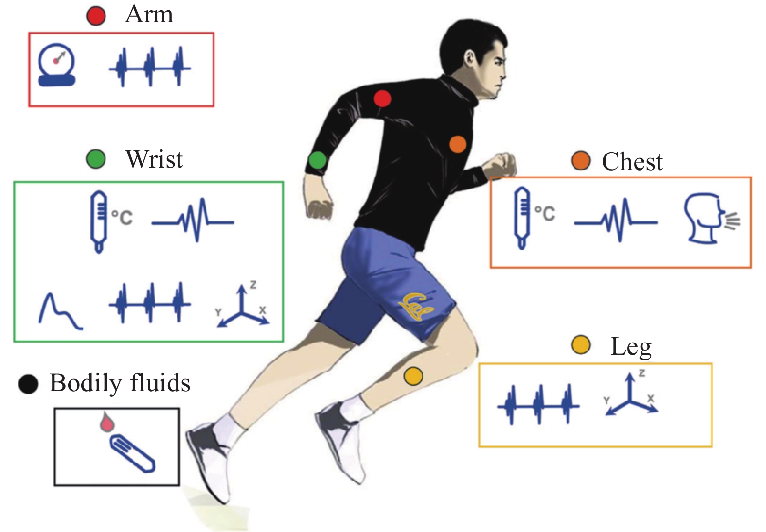
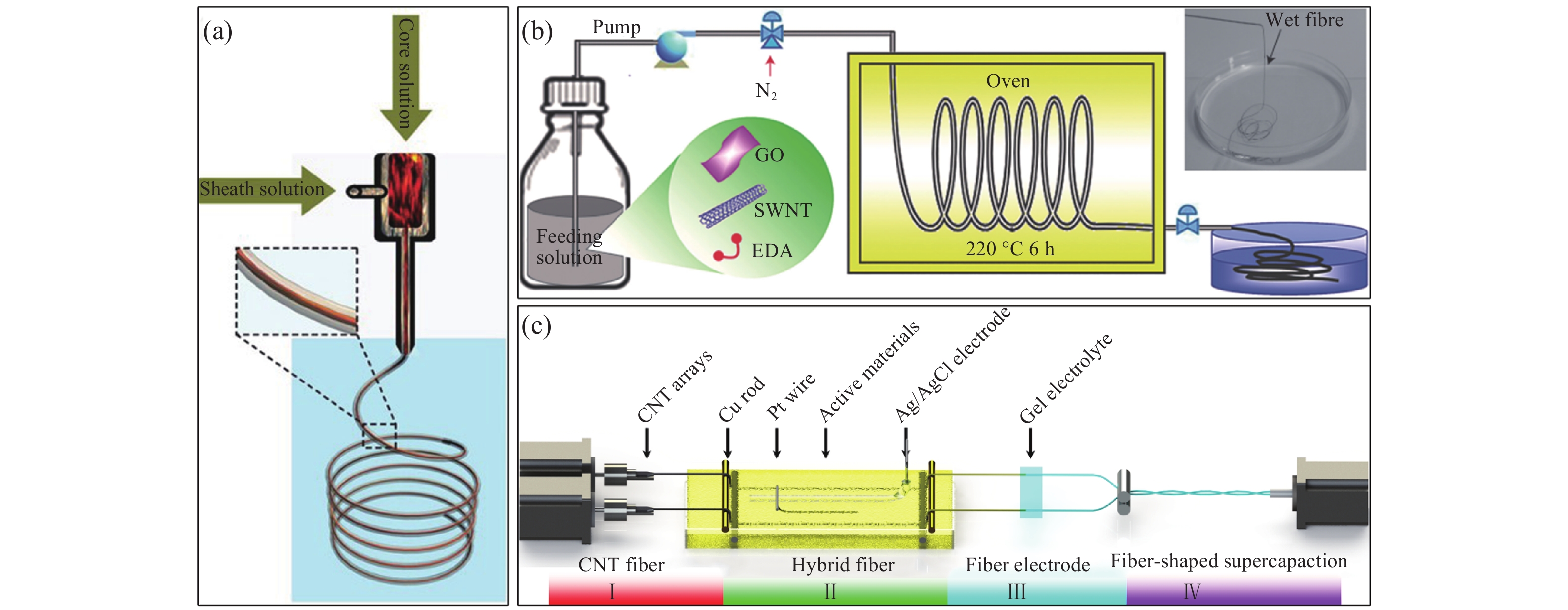
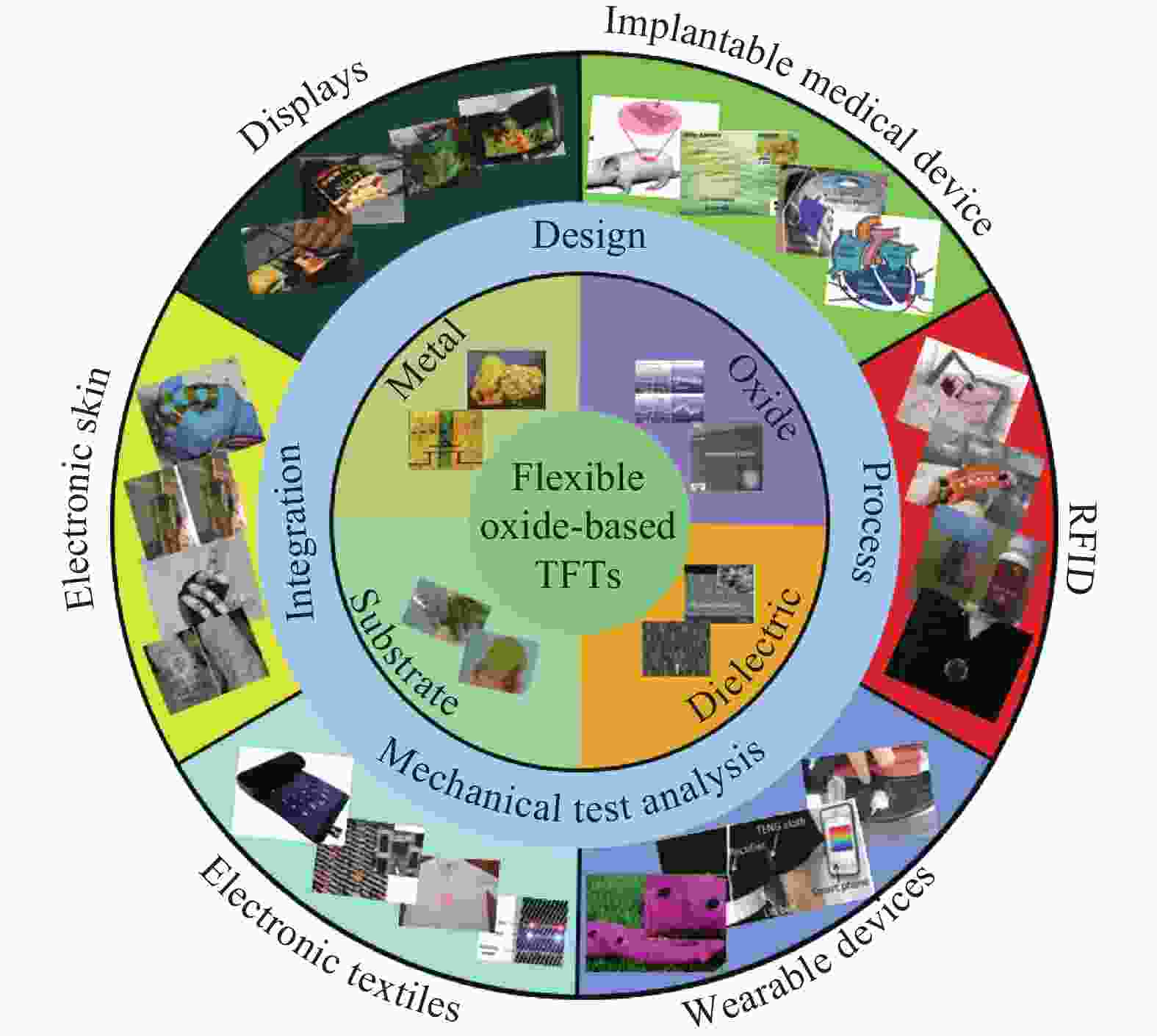
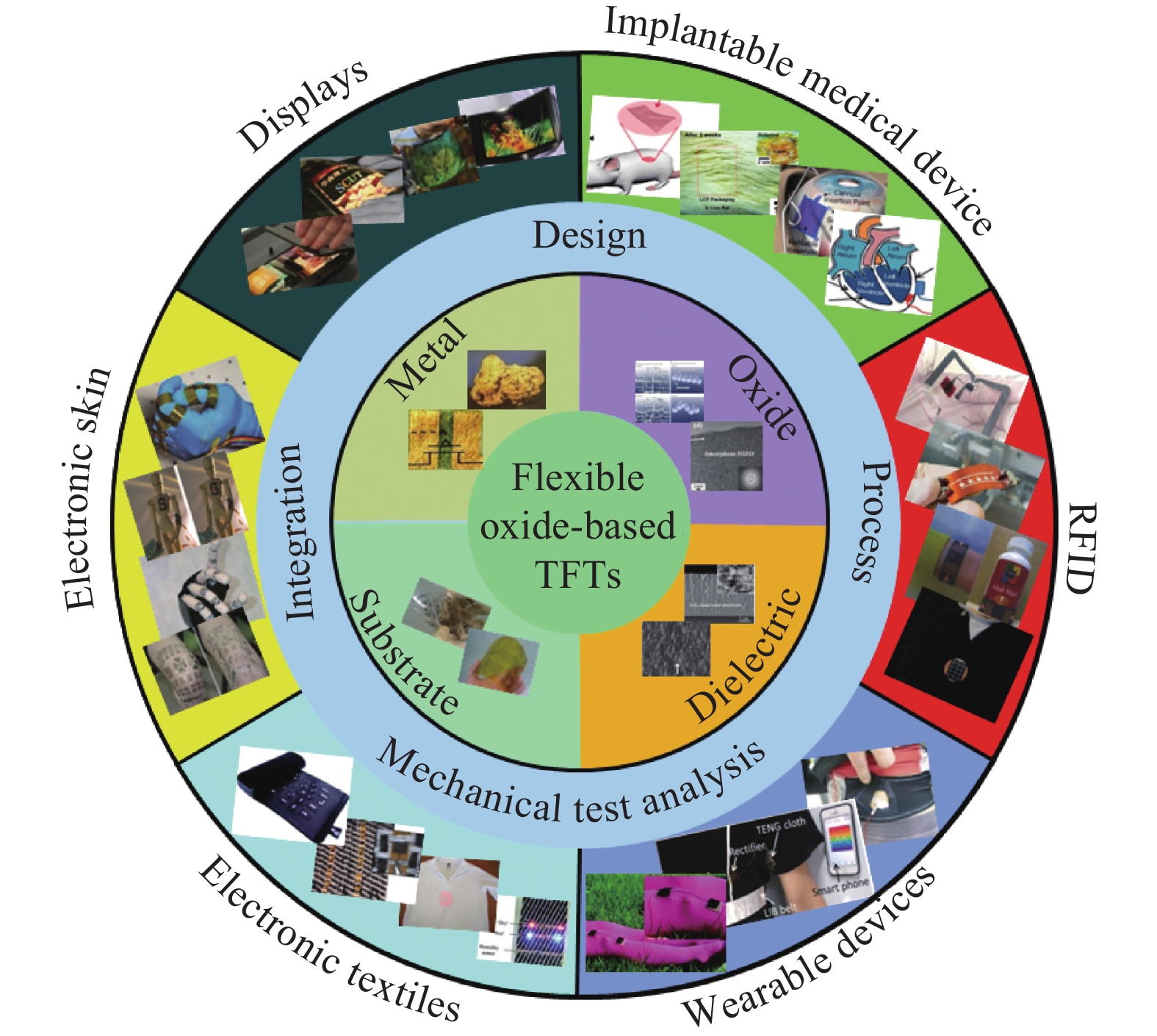
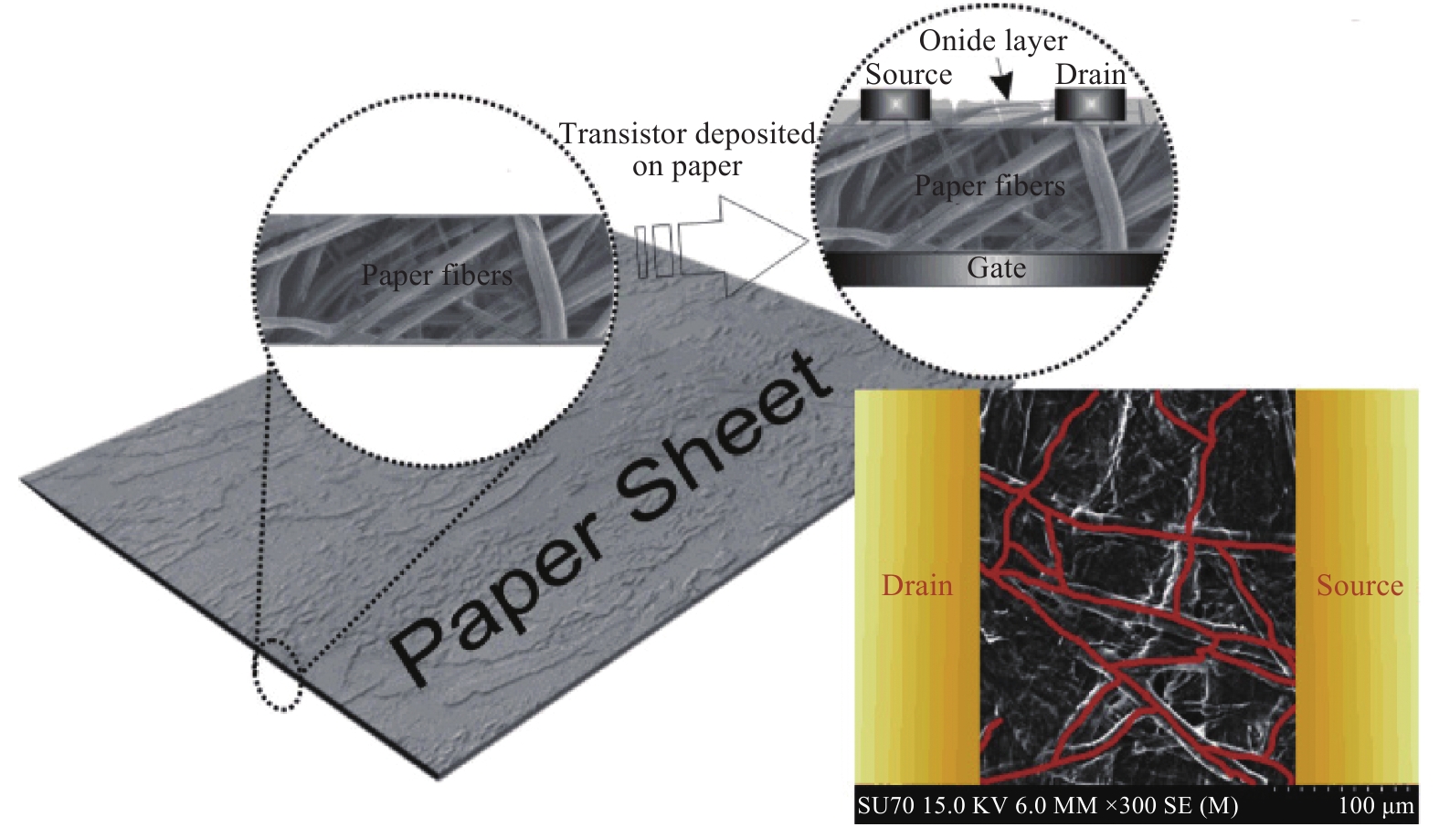
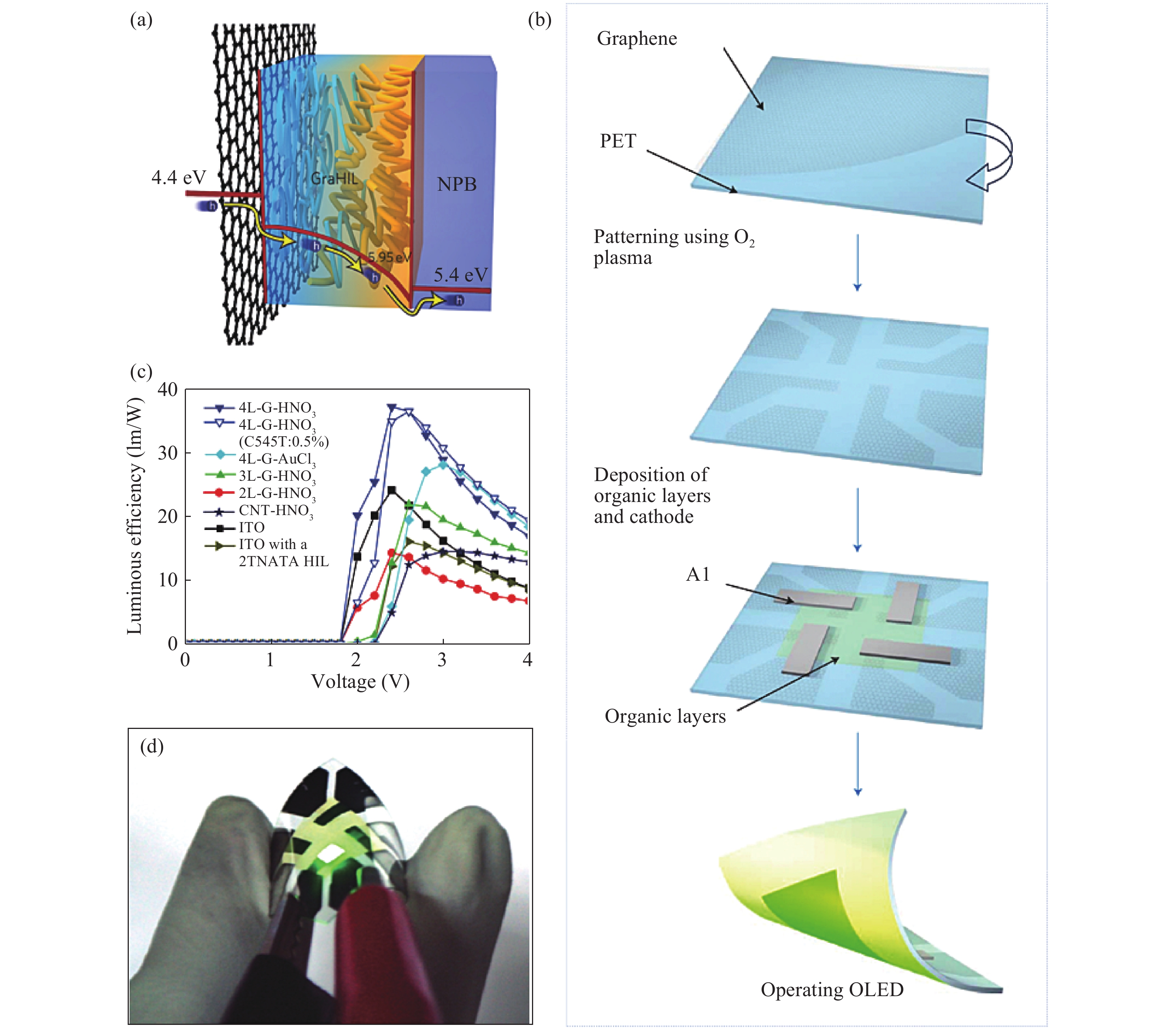
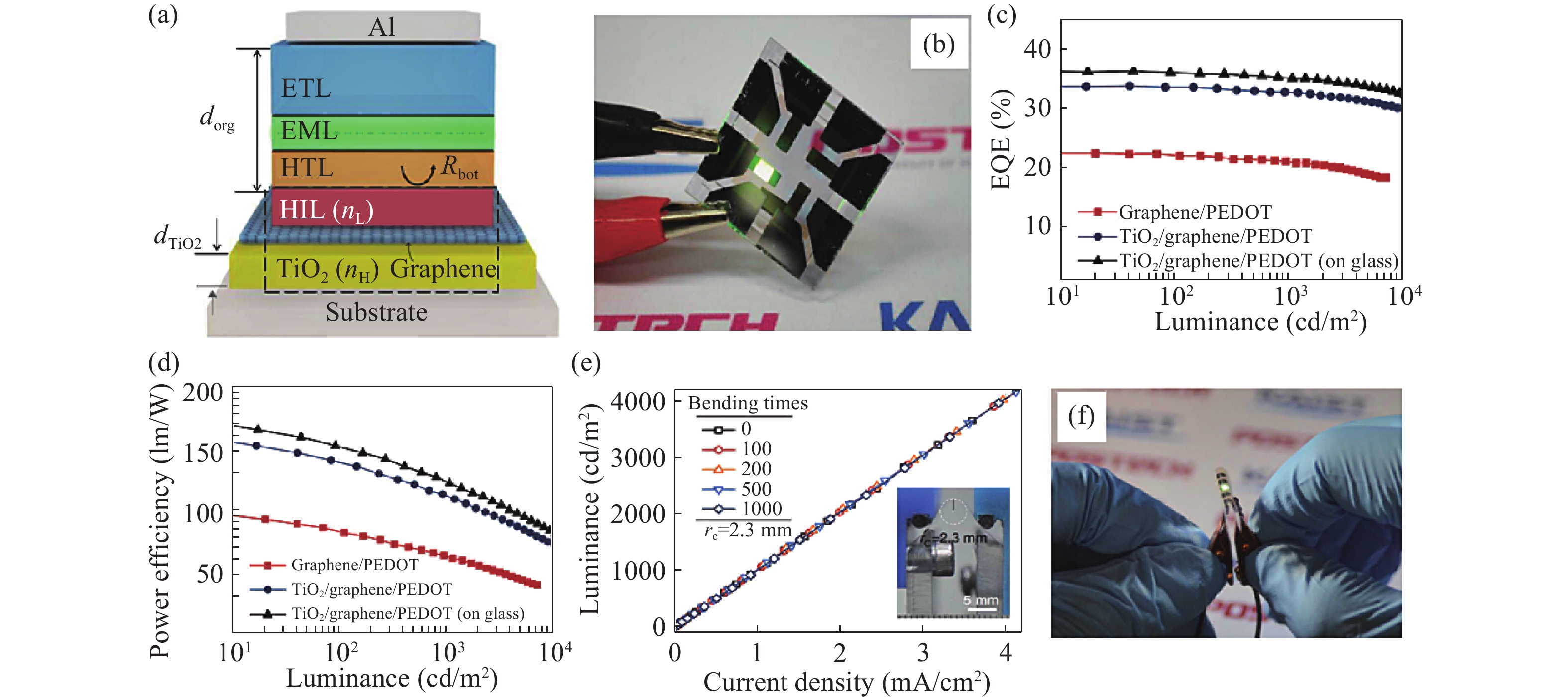
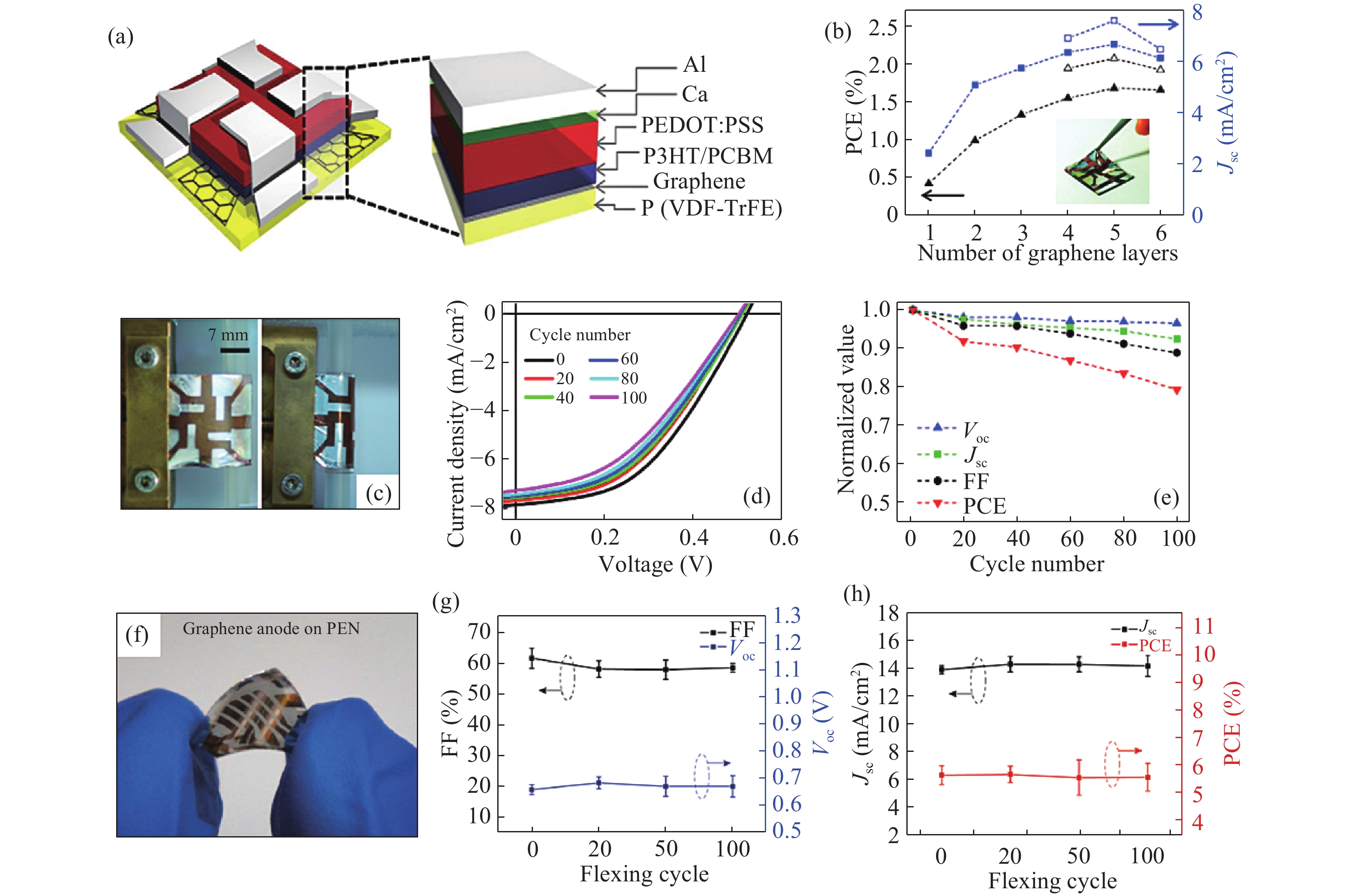
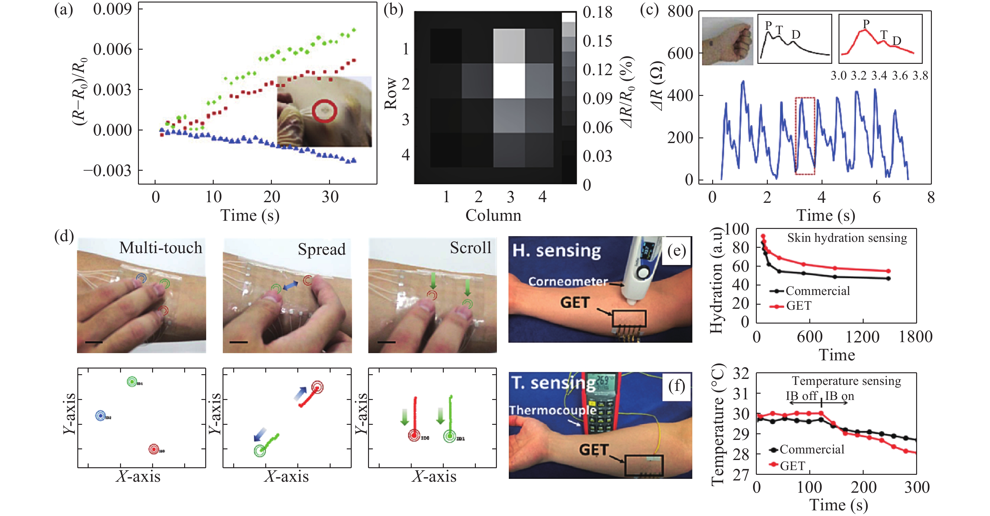
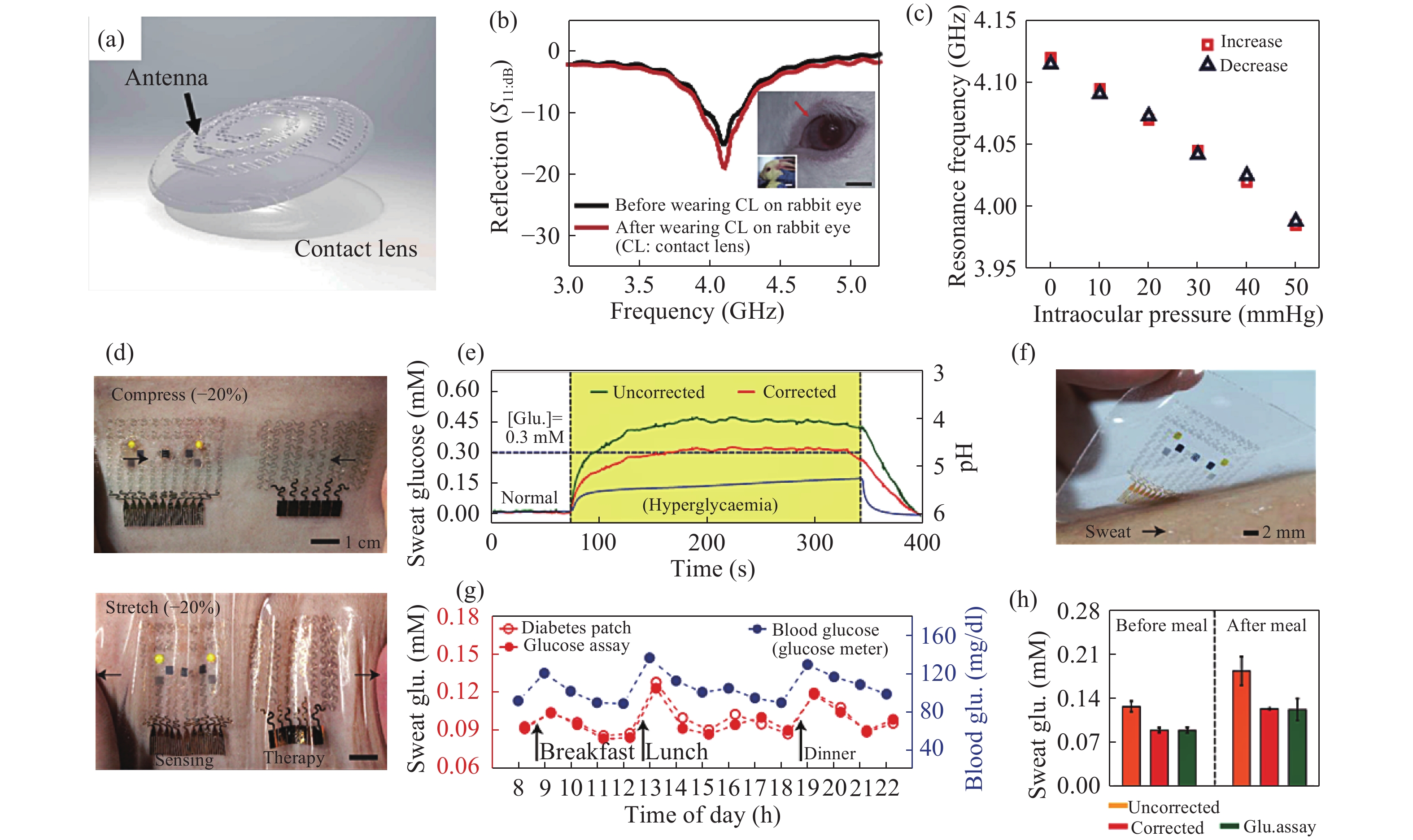
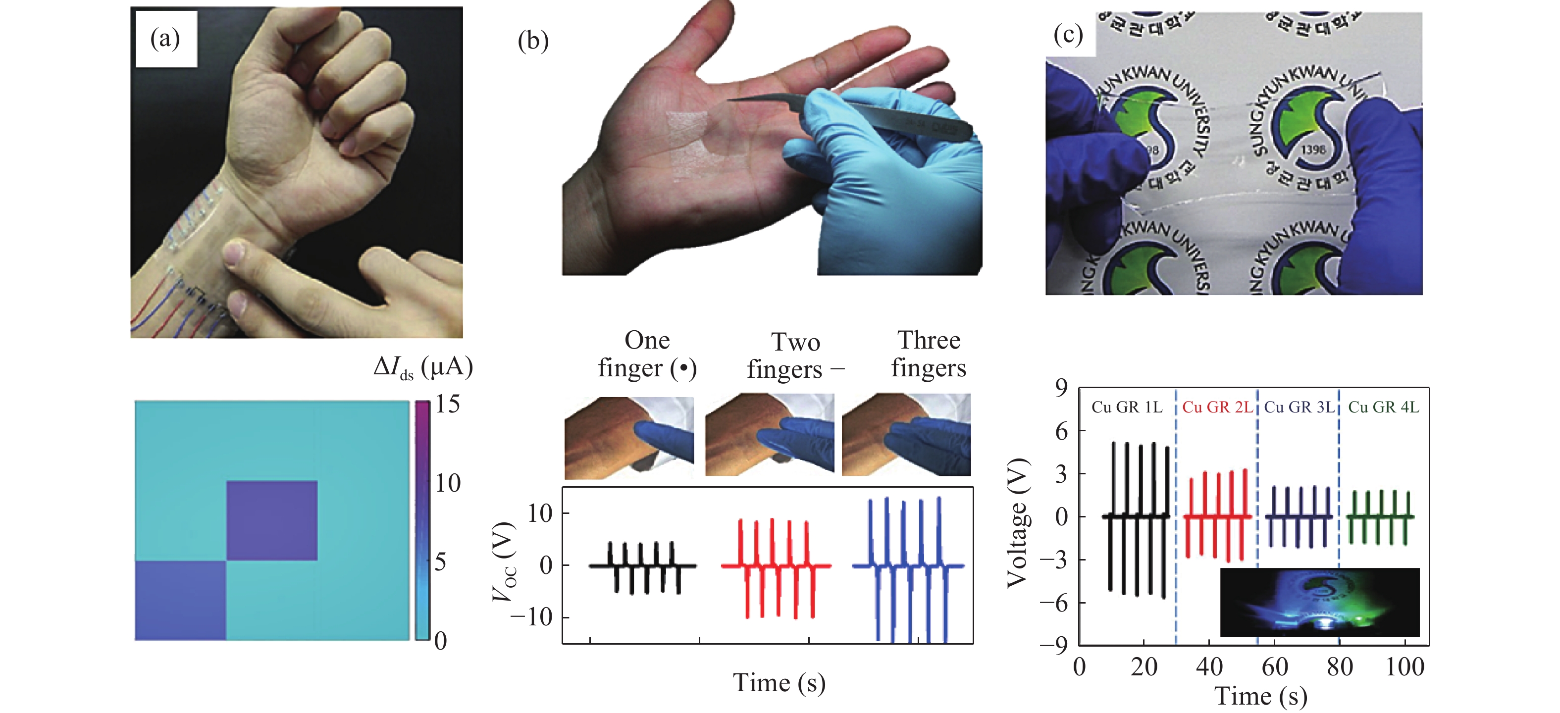
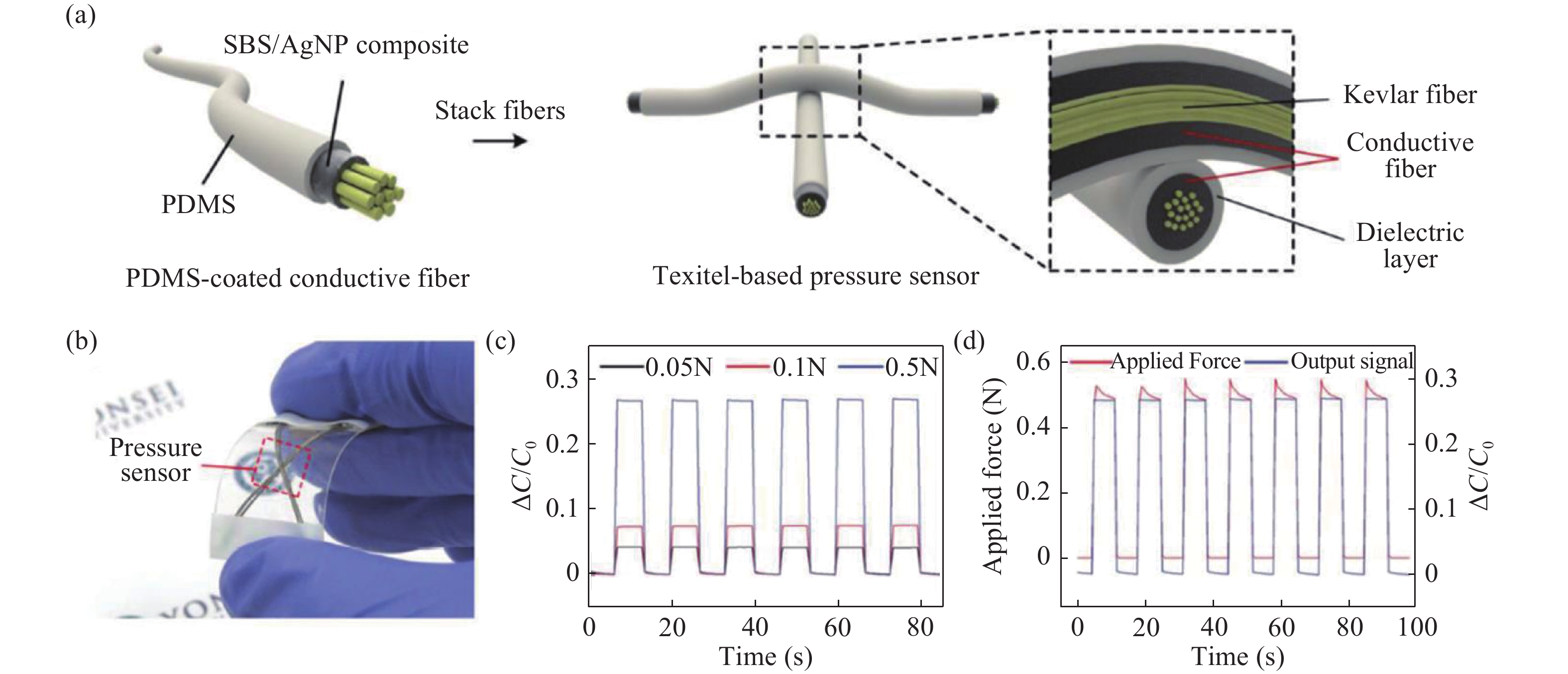
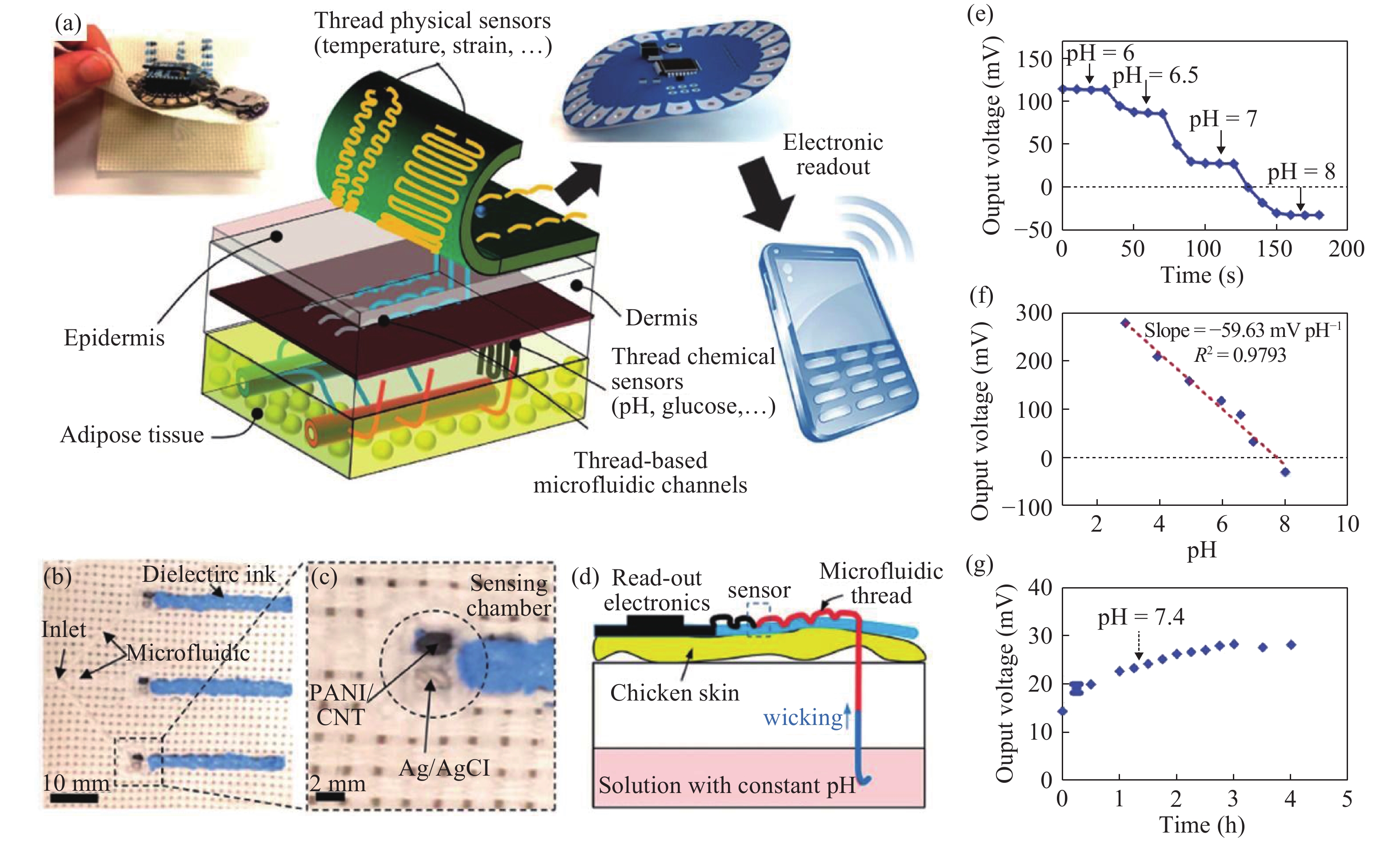
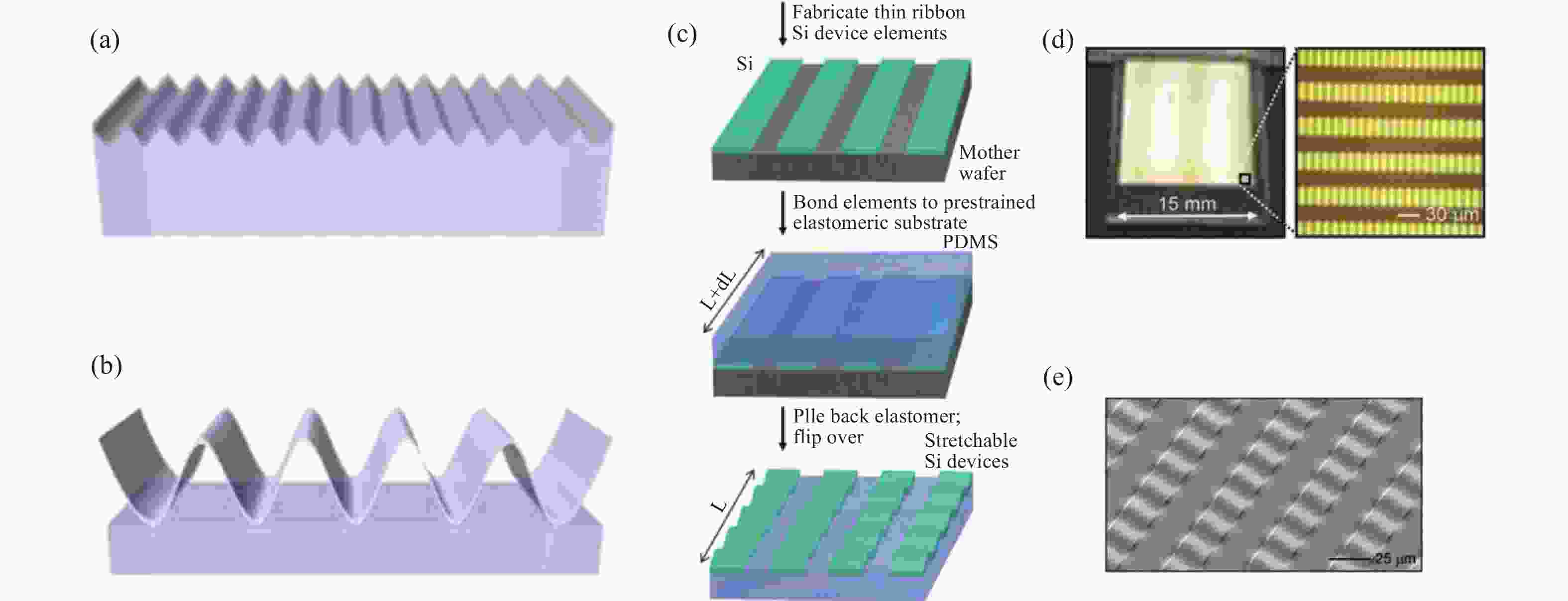
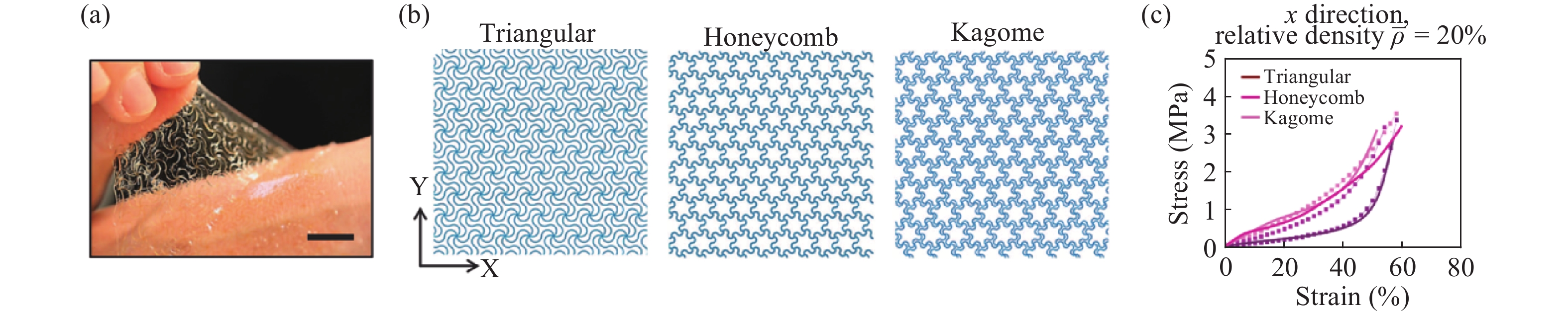
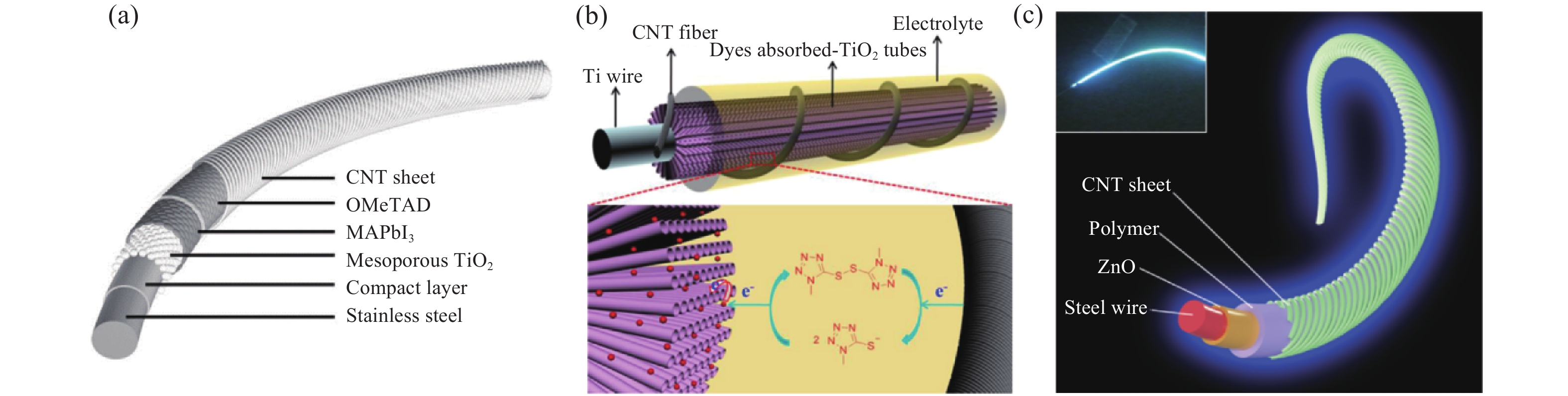
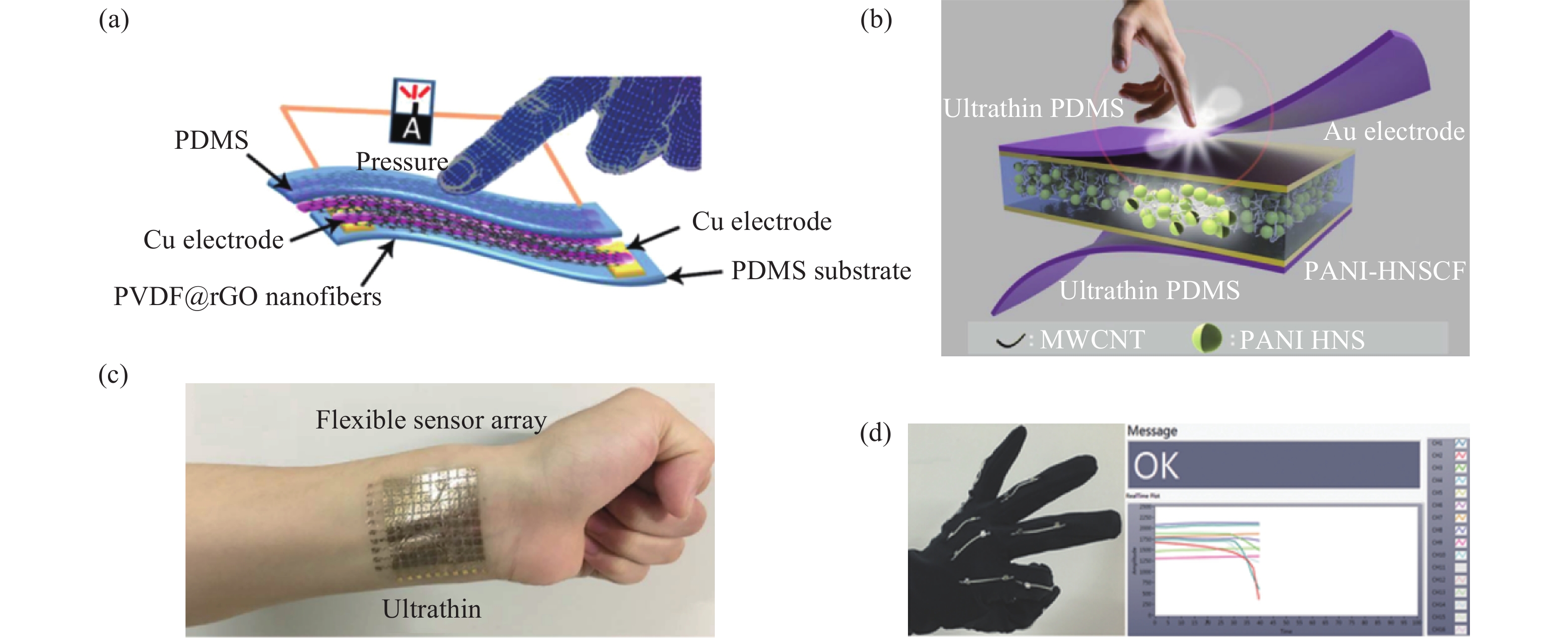
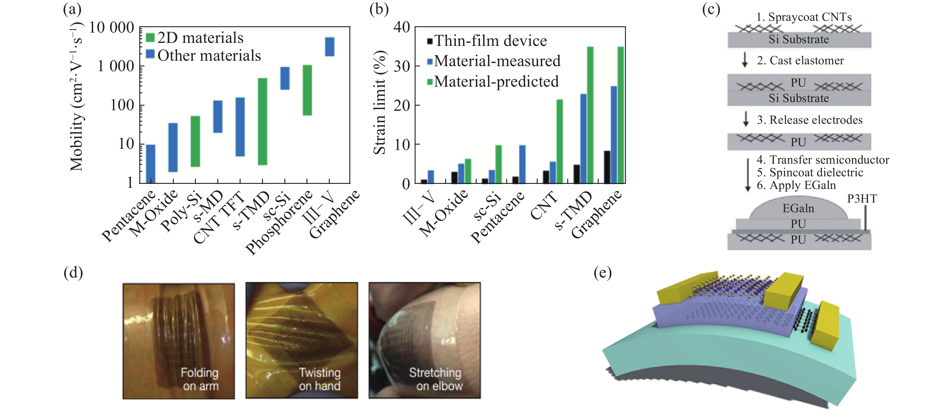
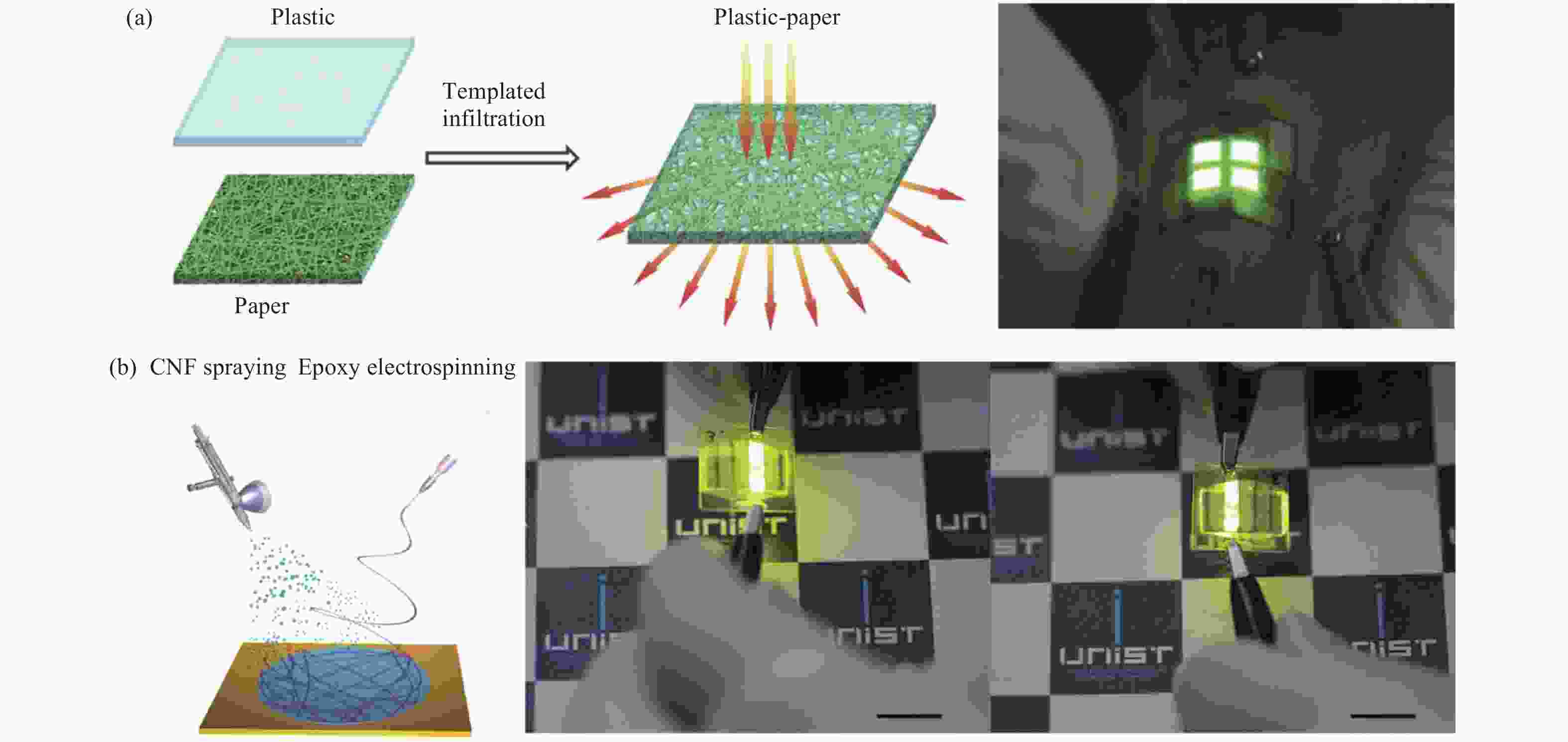
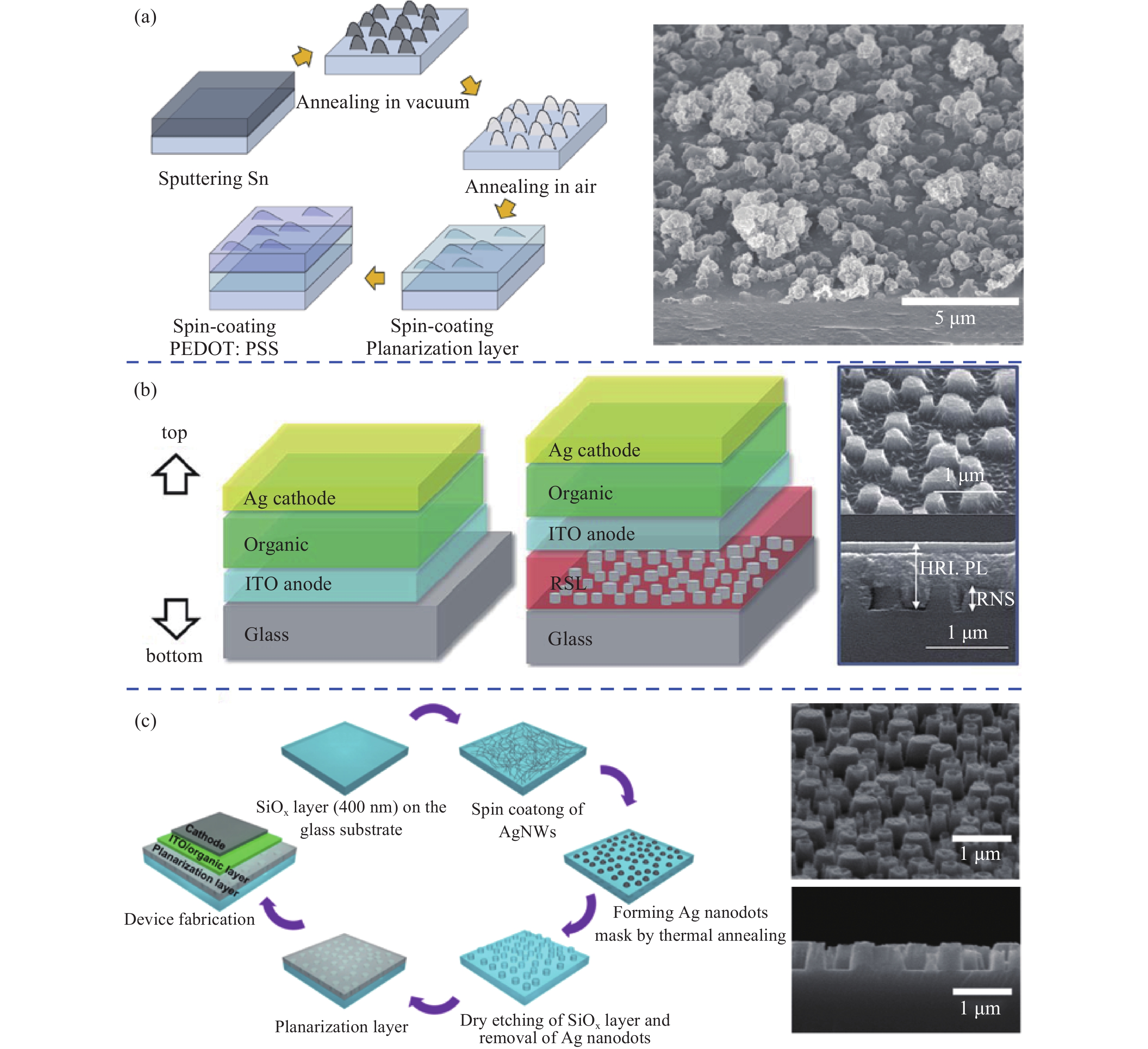
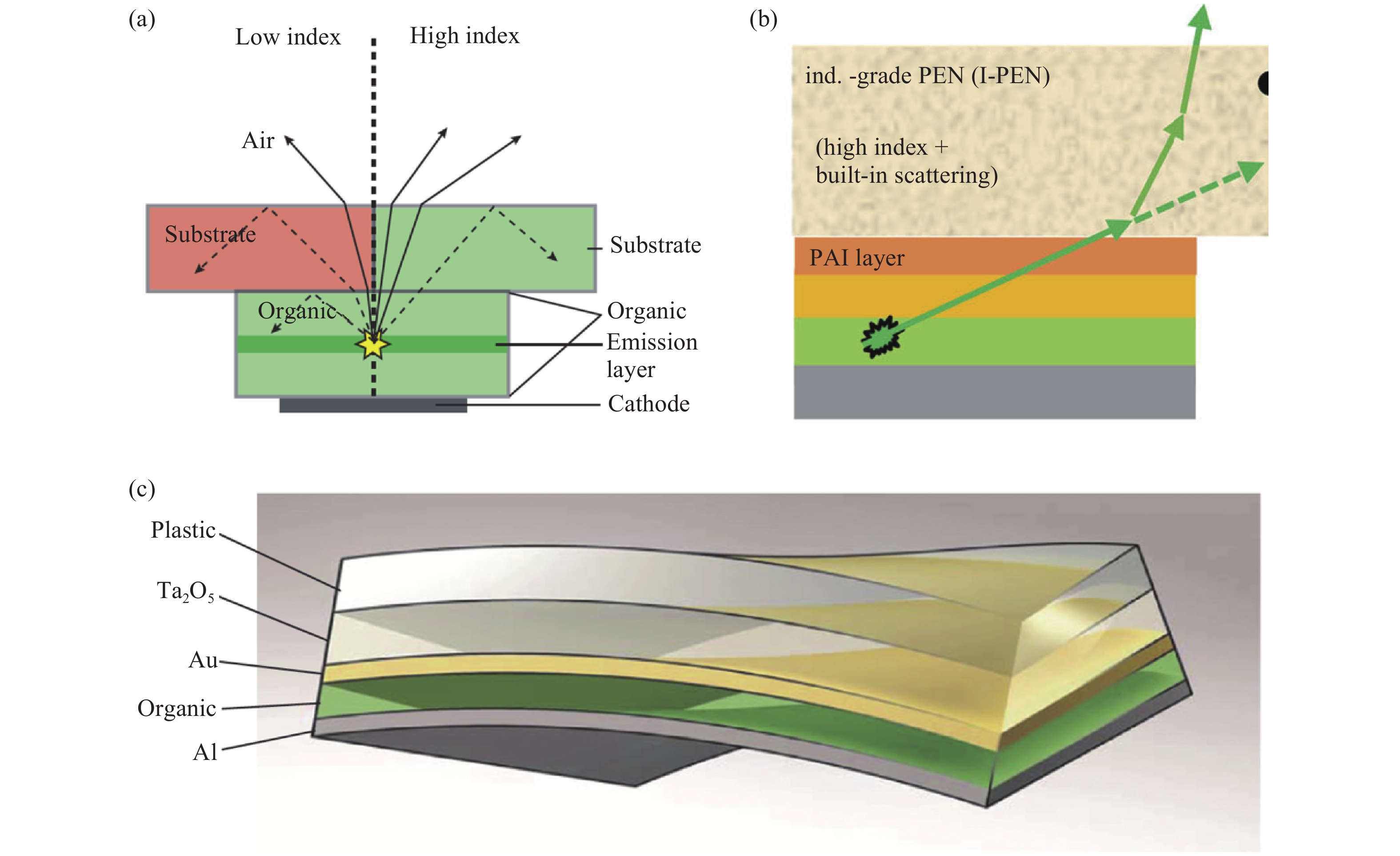
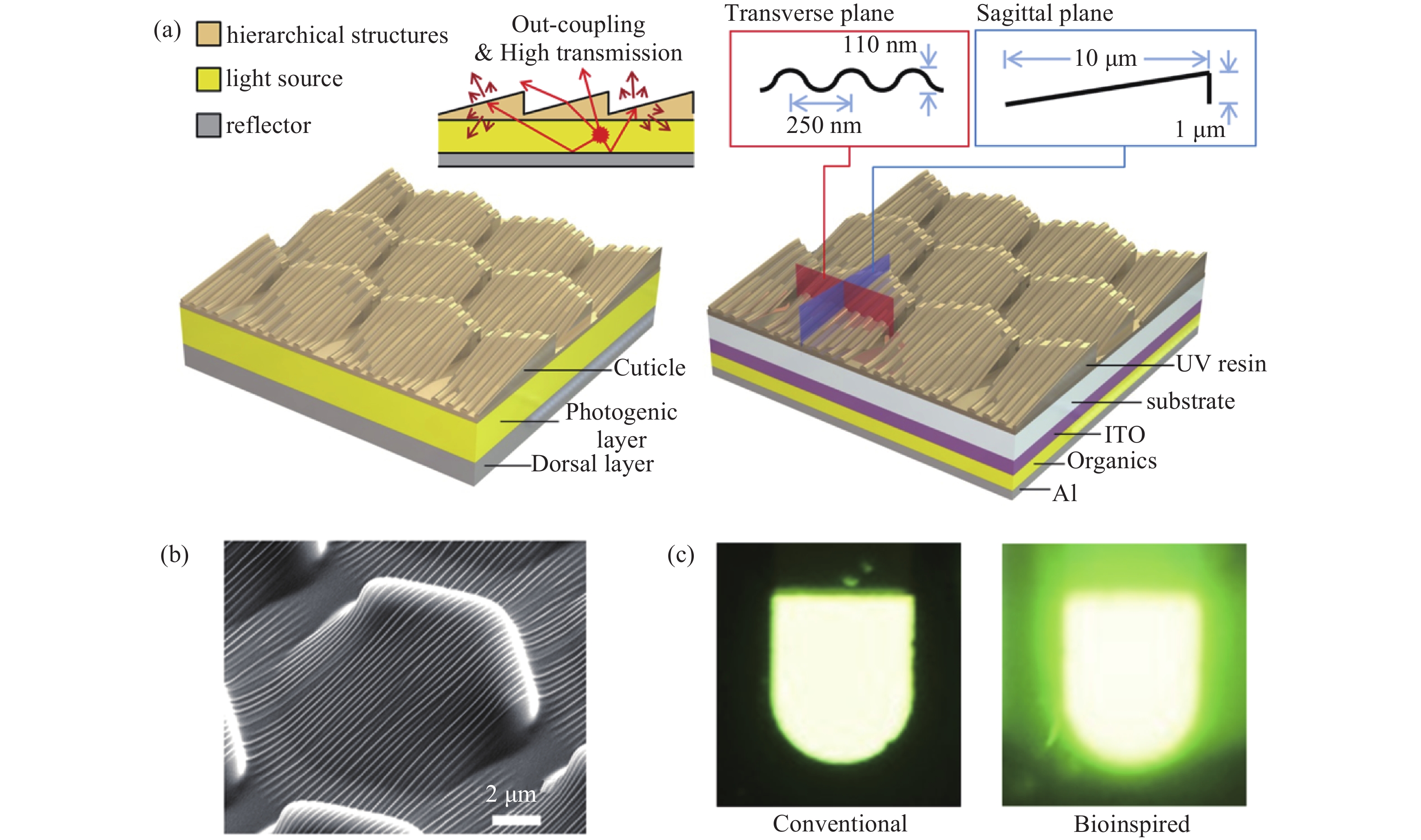
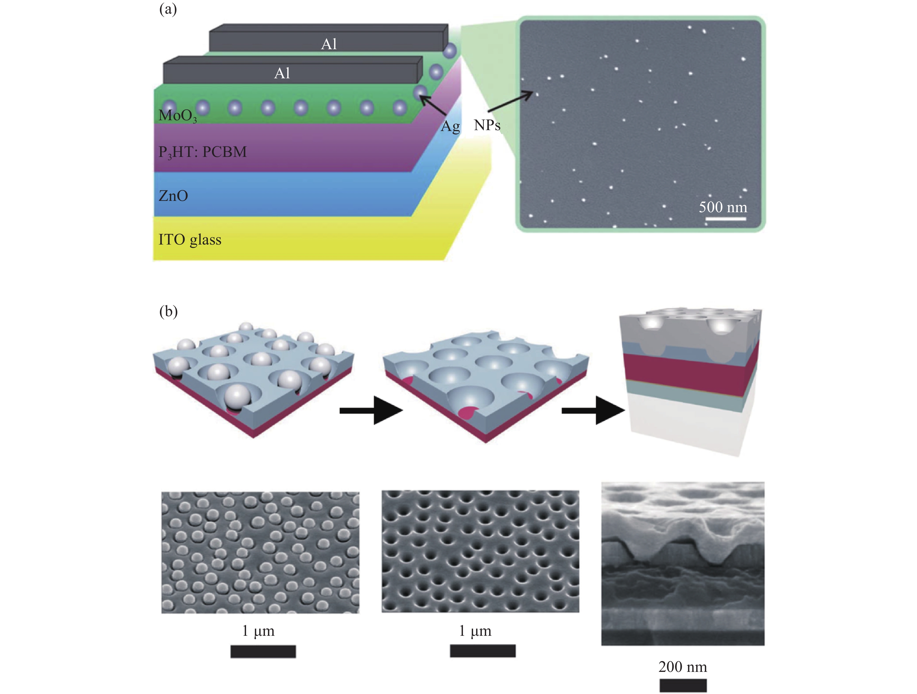
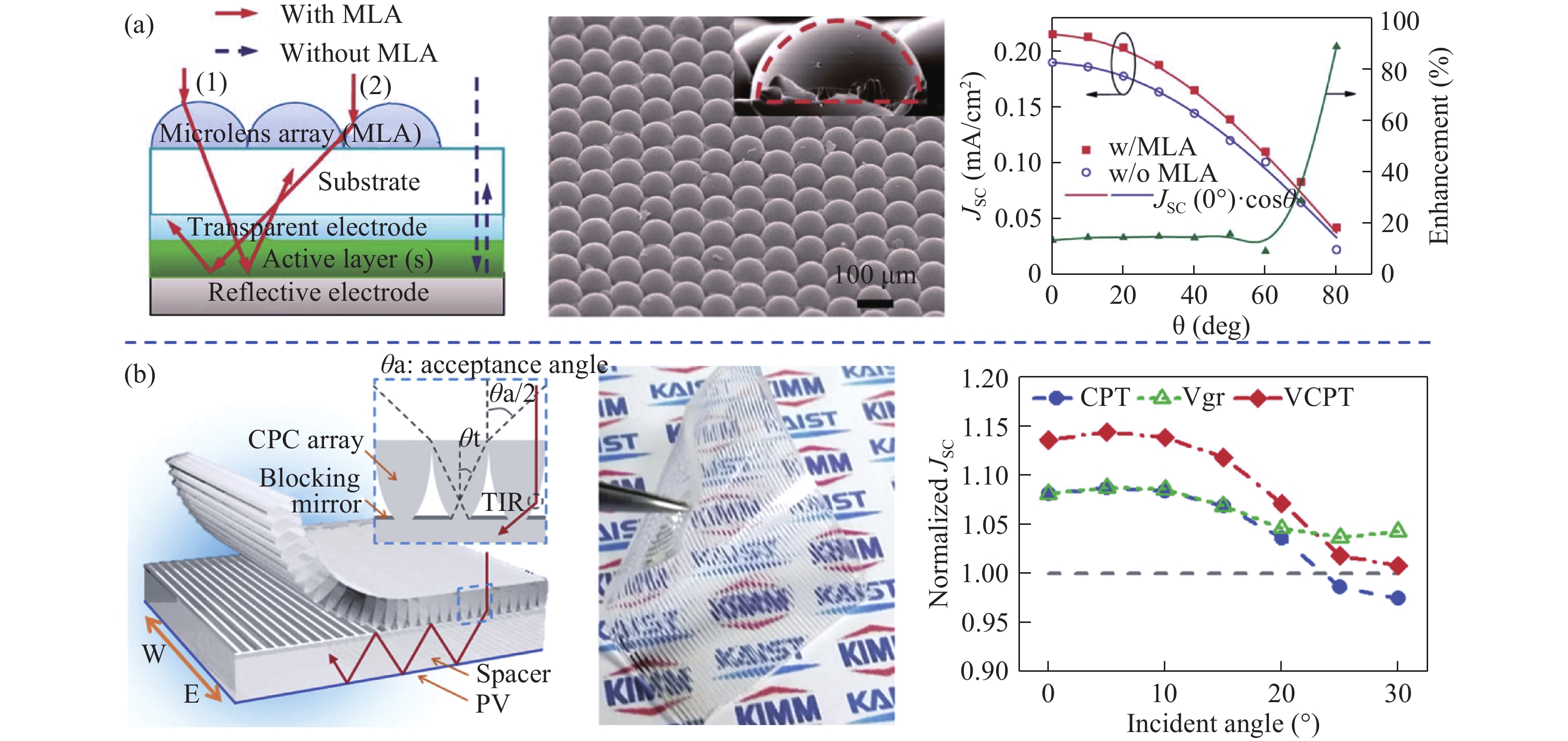
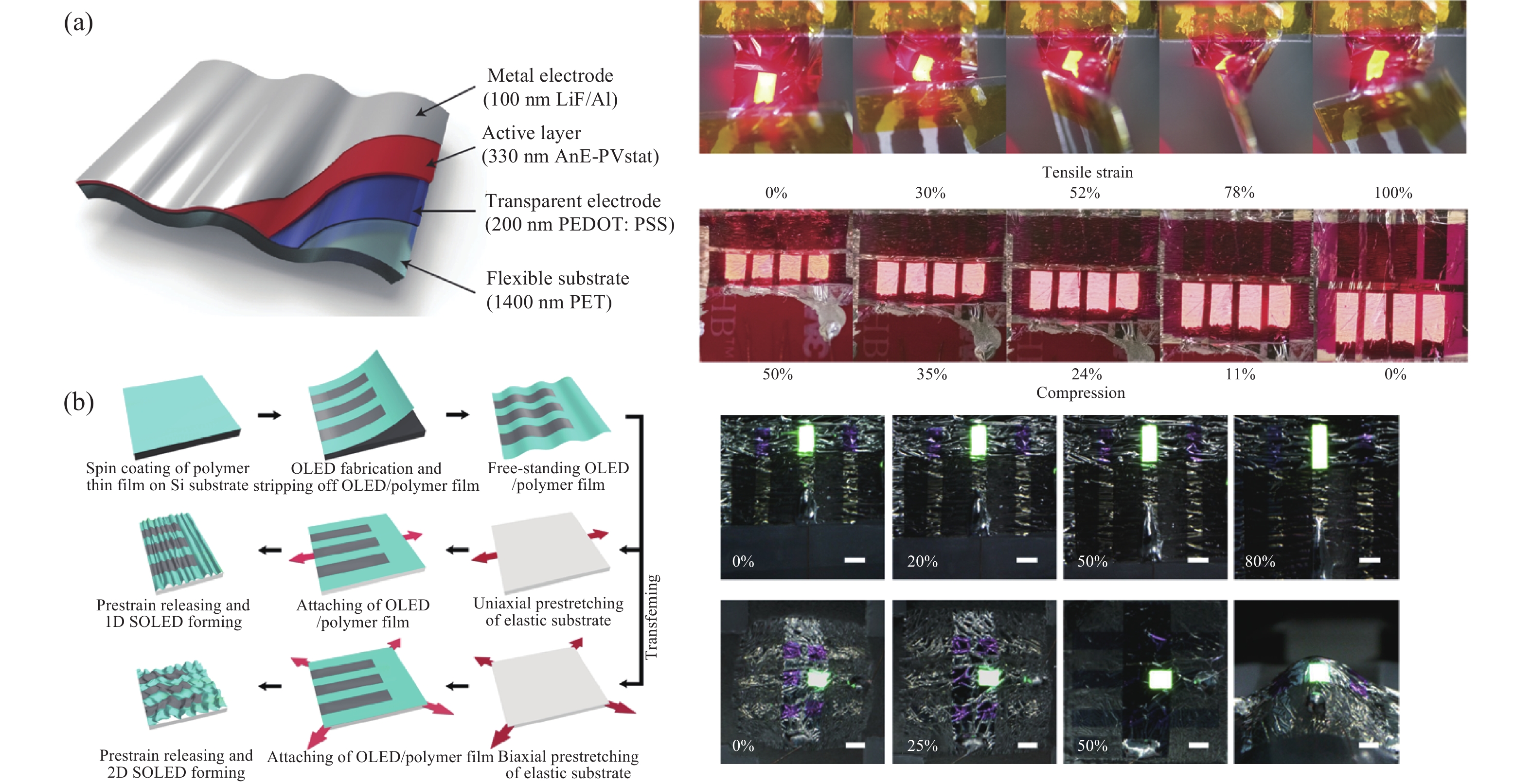
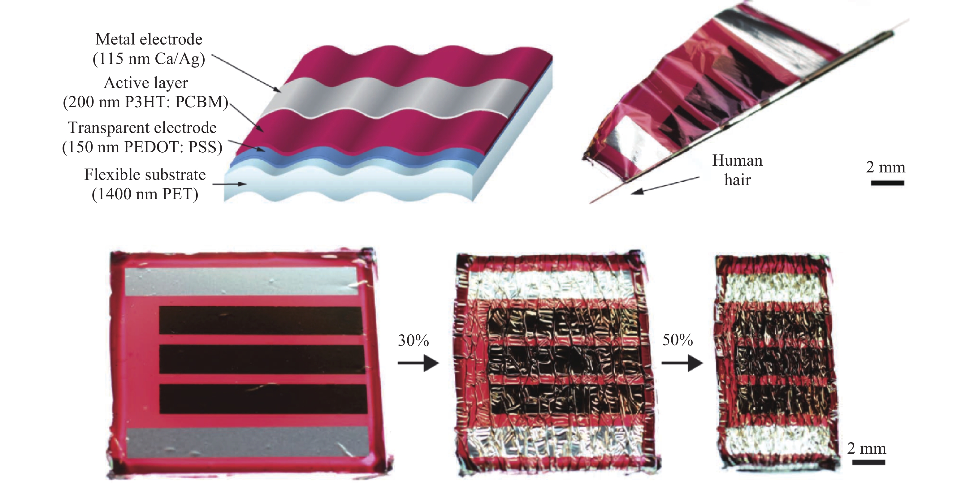
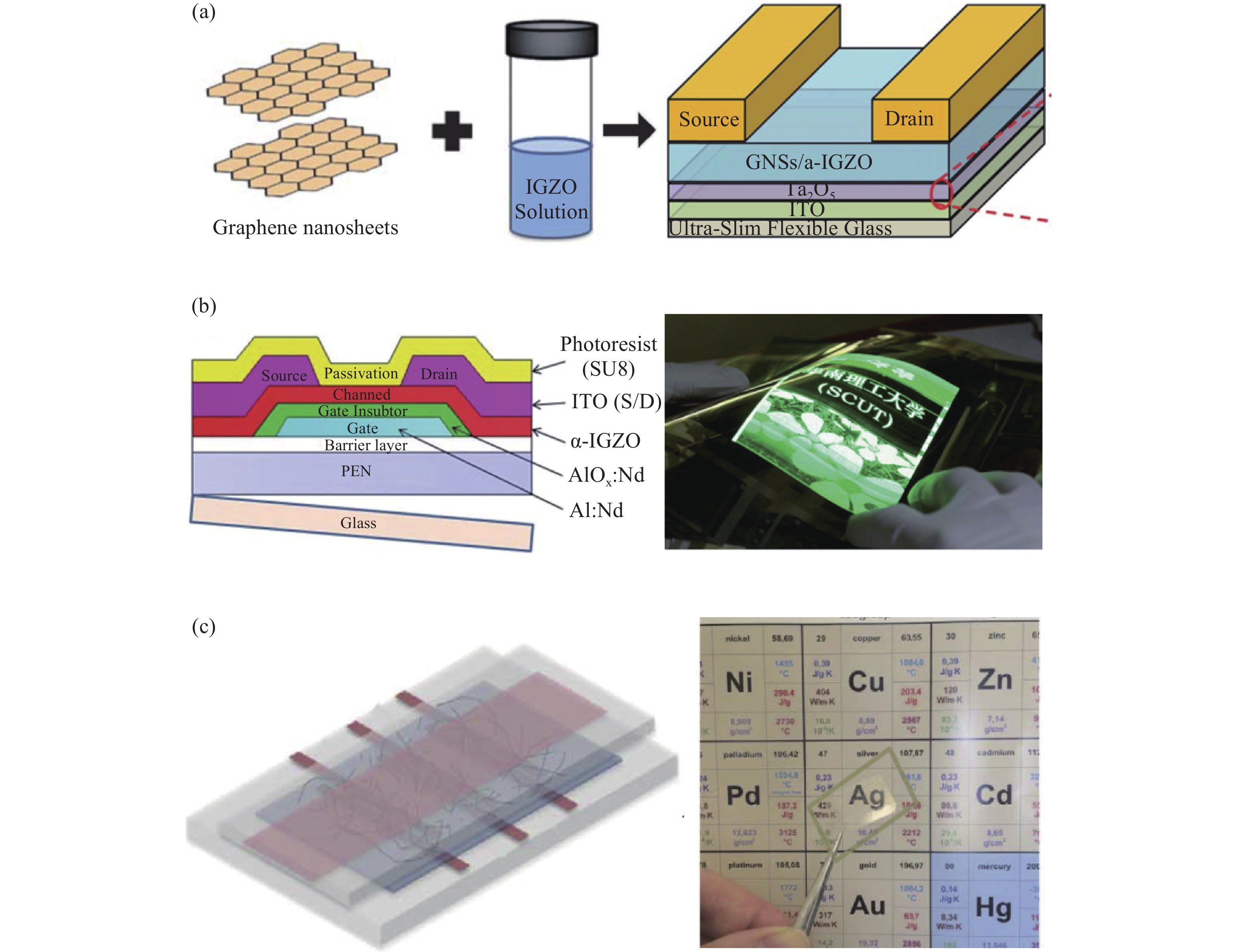
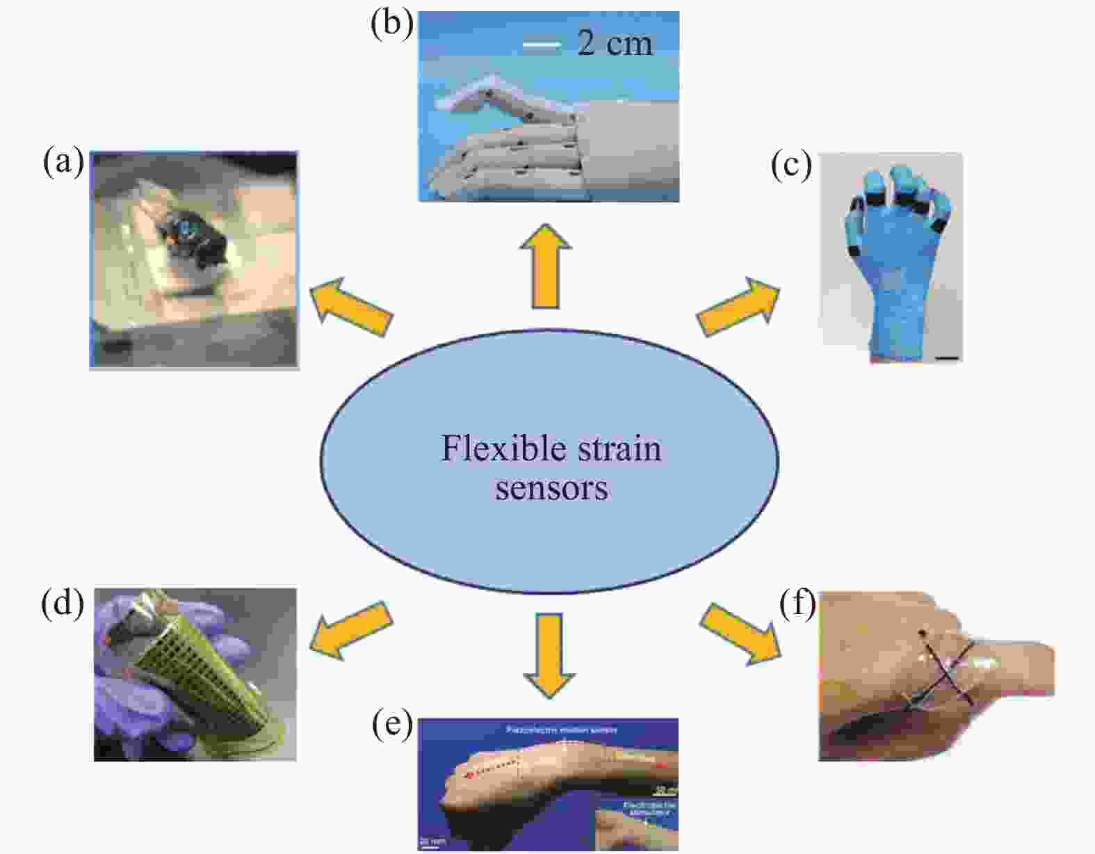
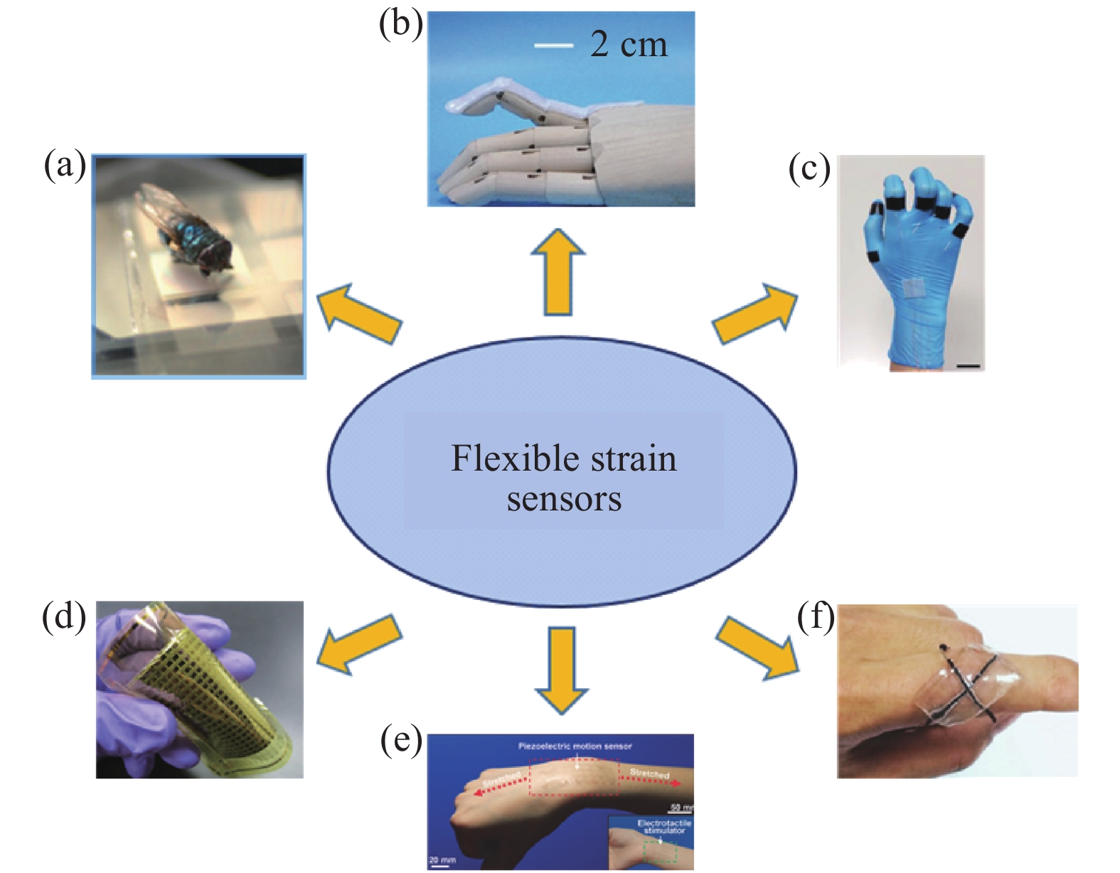
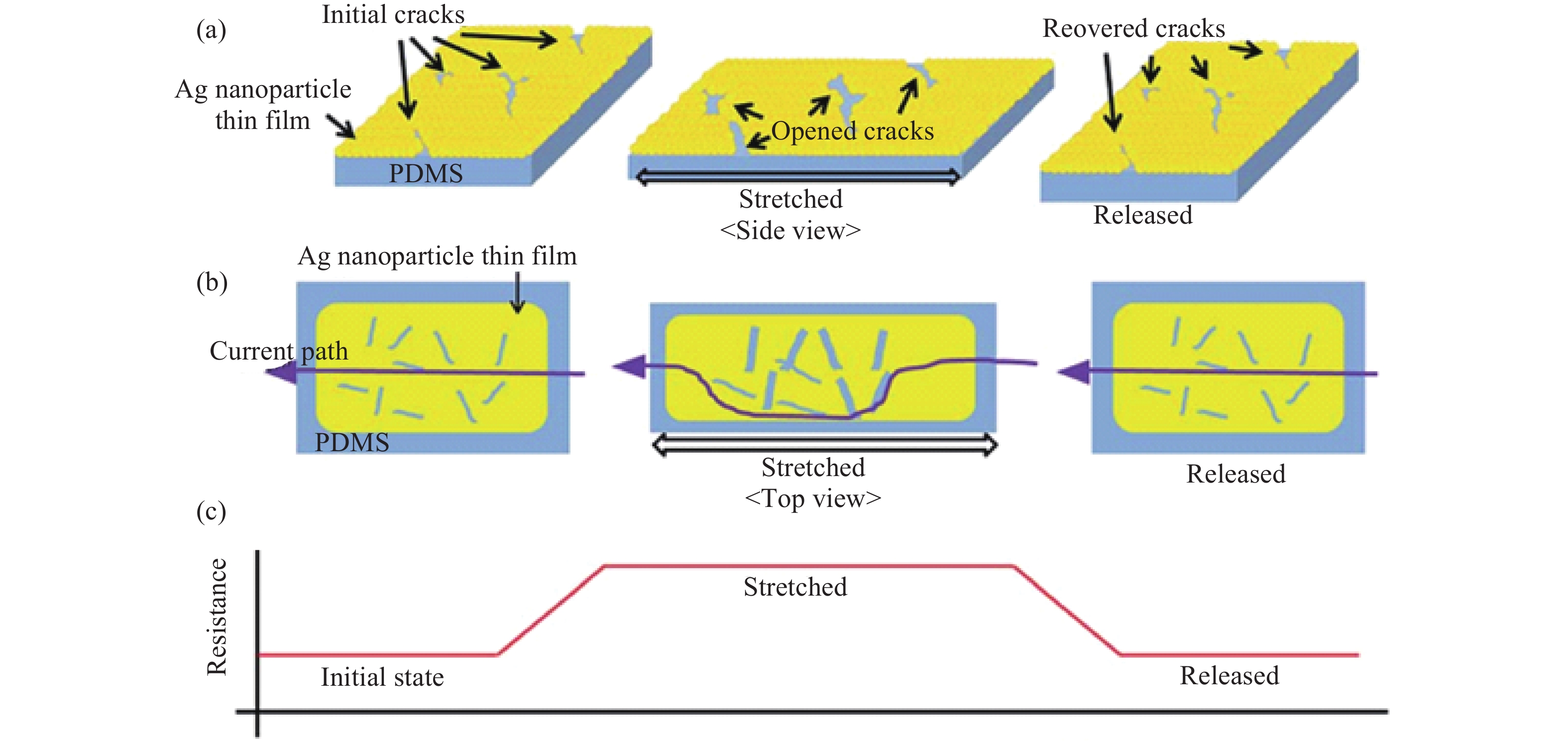
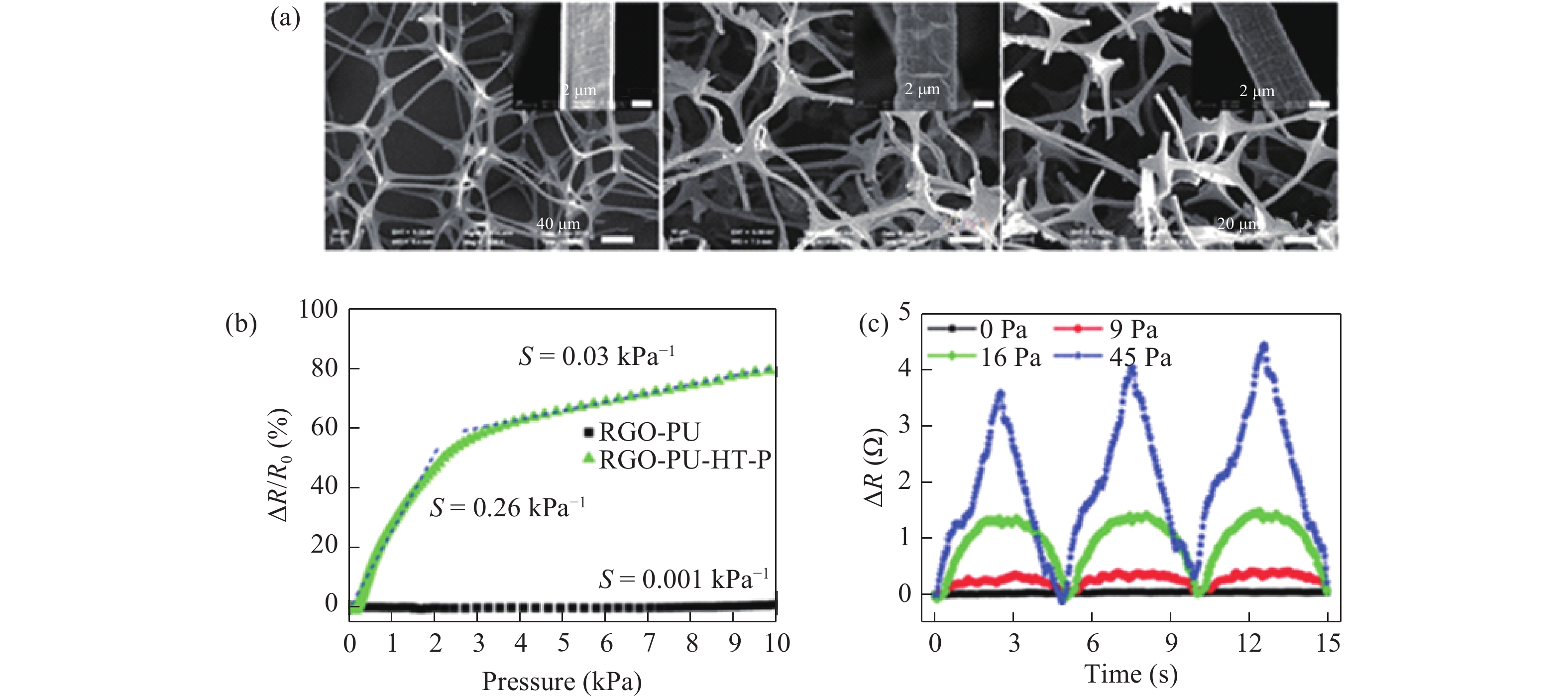
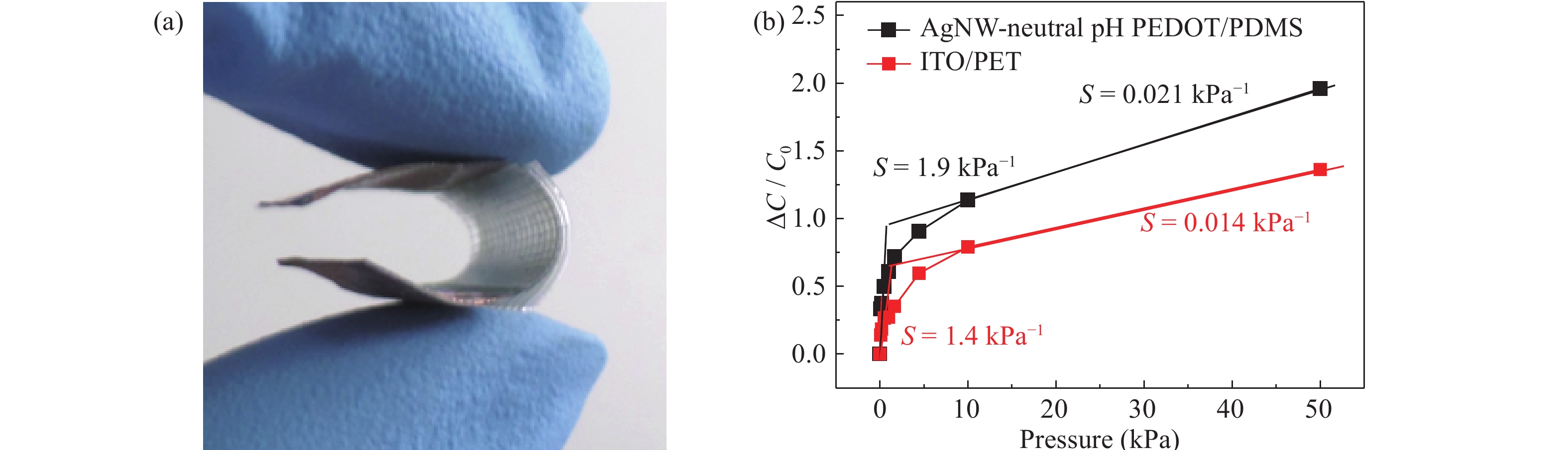
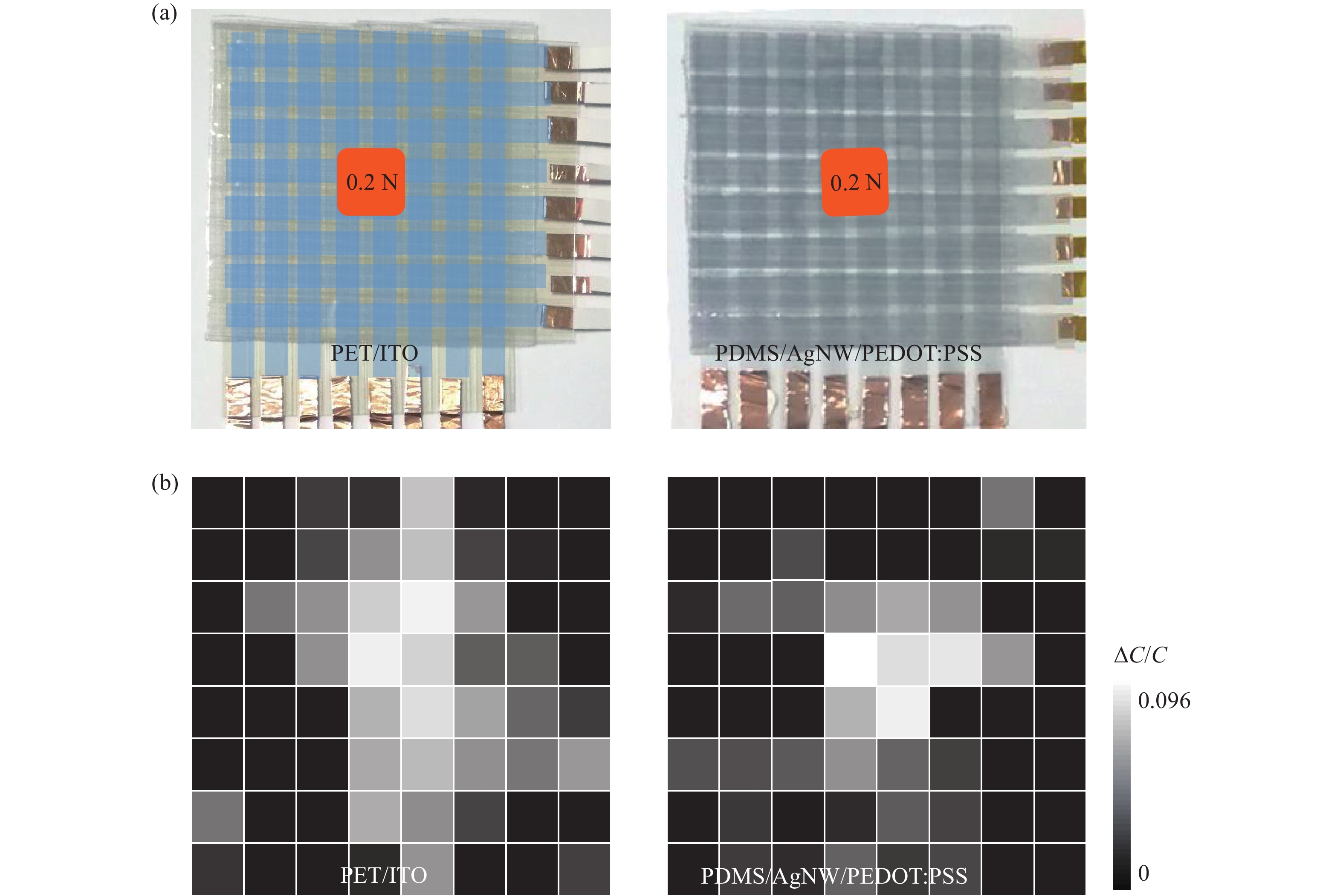
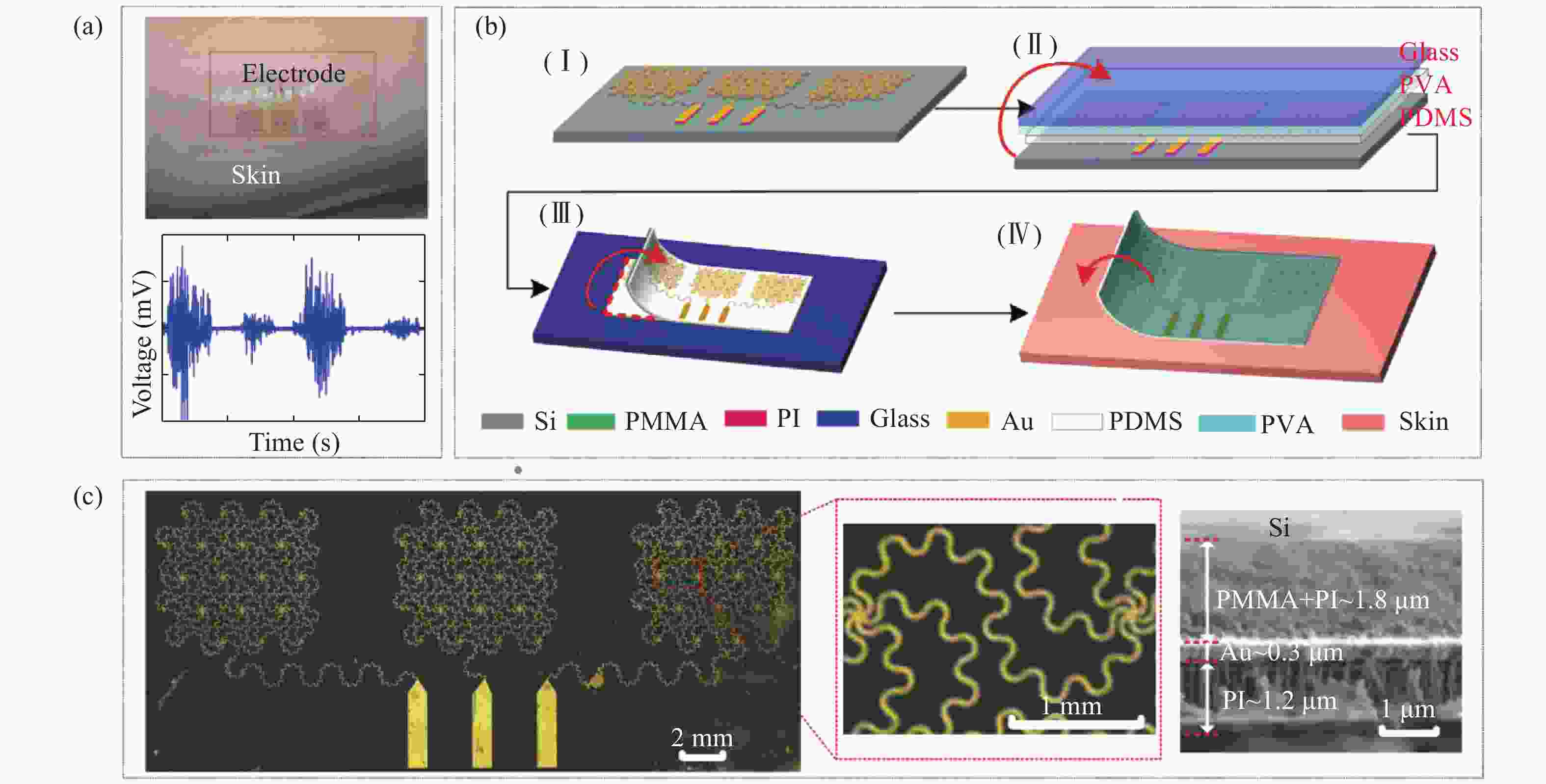
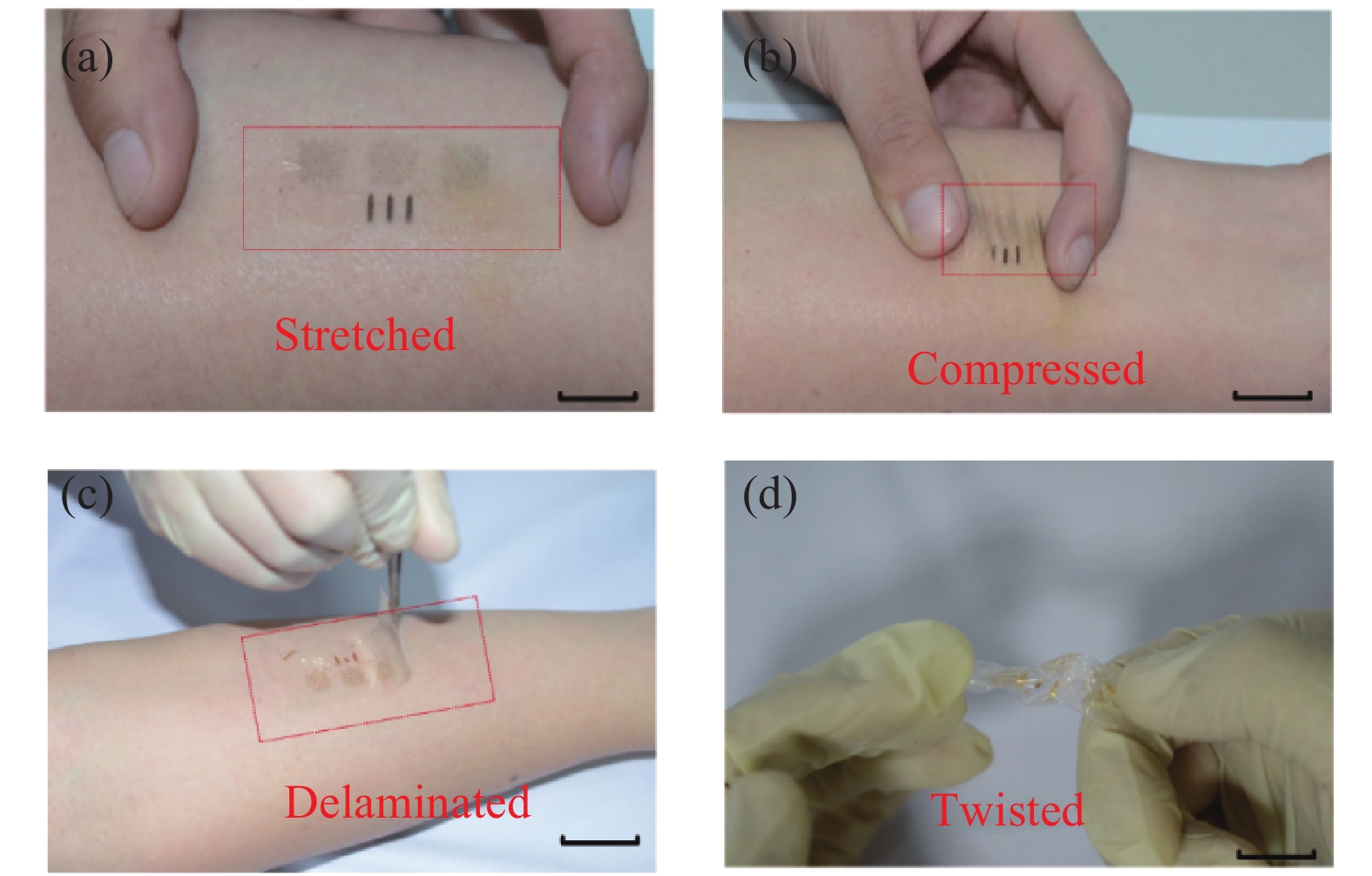
Electronic systems that can cover large areas on flexible/ stretchable substrates have received increasing attention in the past several years because they enable new classes of applications that lie outside those easily addressed with wafer-based microelectronics. Some attractive examples include flexible displays, flexible solar cells, electronic textiles, sensory skins, detectors, active antennas, etc. The field expends very fast and great developments have been obtained during the past several years. Recent exciting progresses such as highly flexible/stretchable E-skins, large area flexible displays, highly sensitive sensors, wearable electronic devices suggest that there are still a lot of room needs to be exploited including materials, devices and systems.
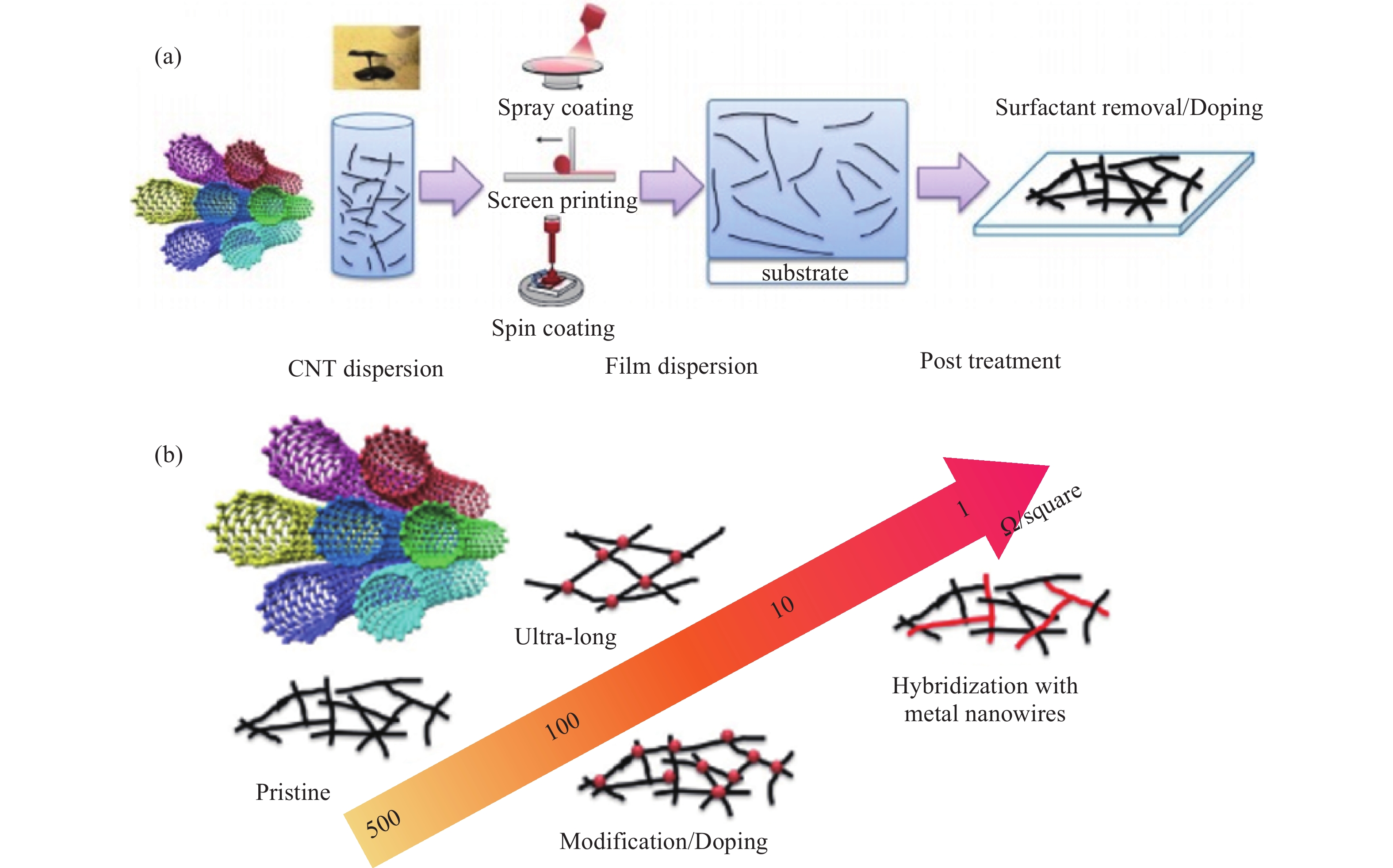
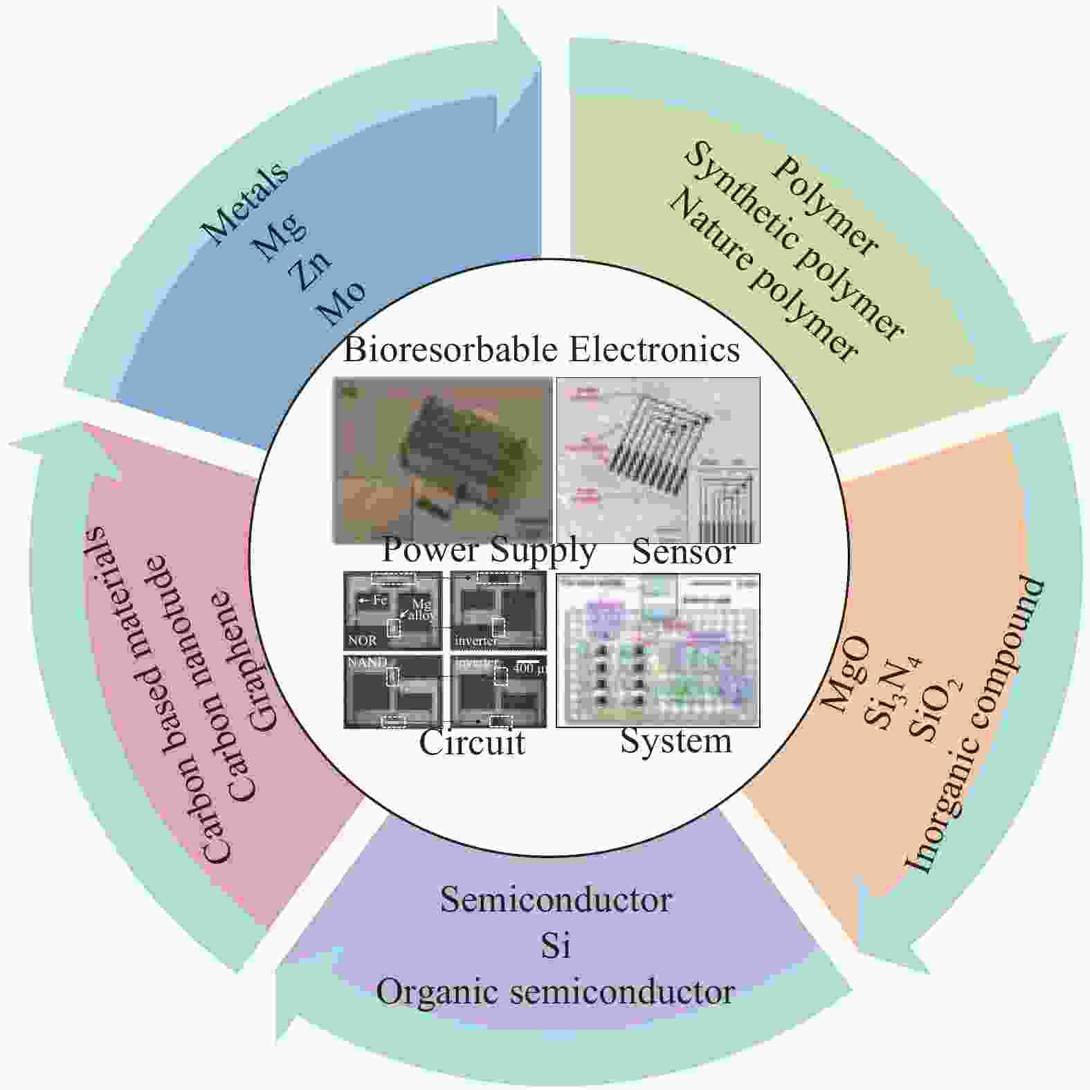
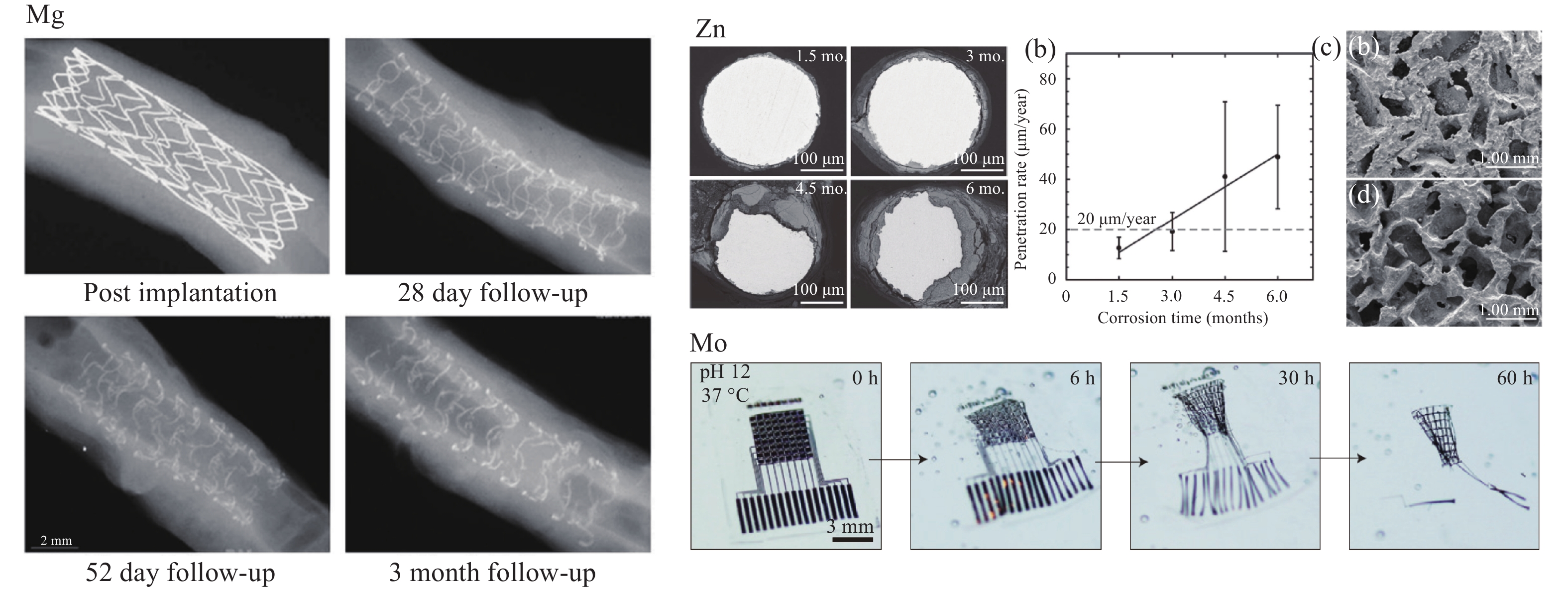
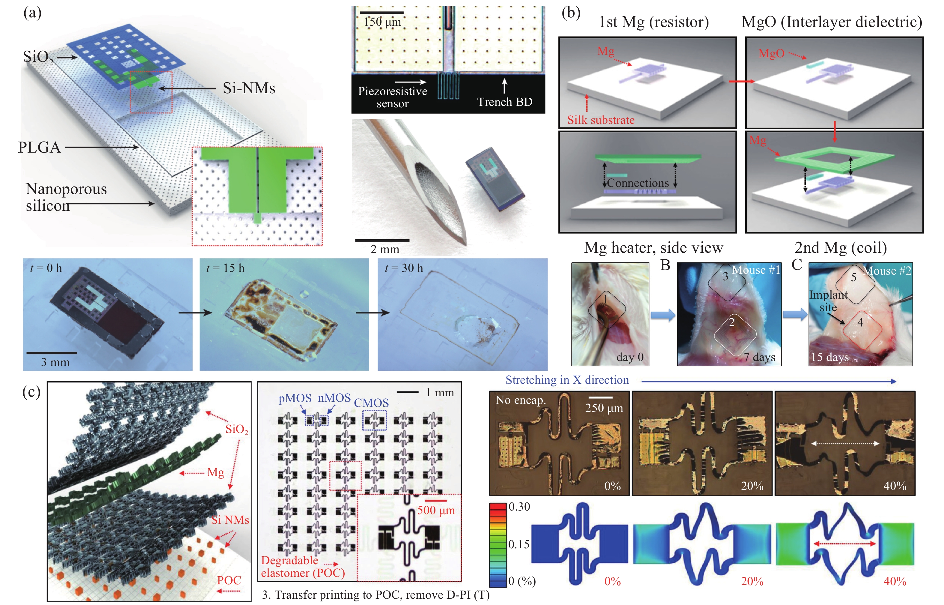
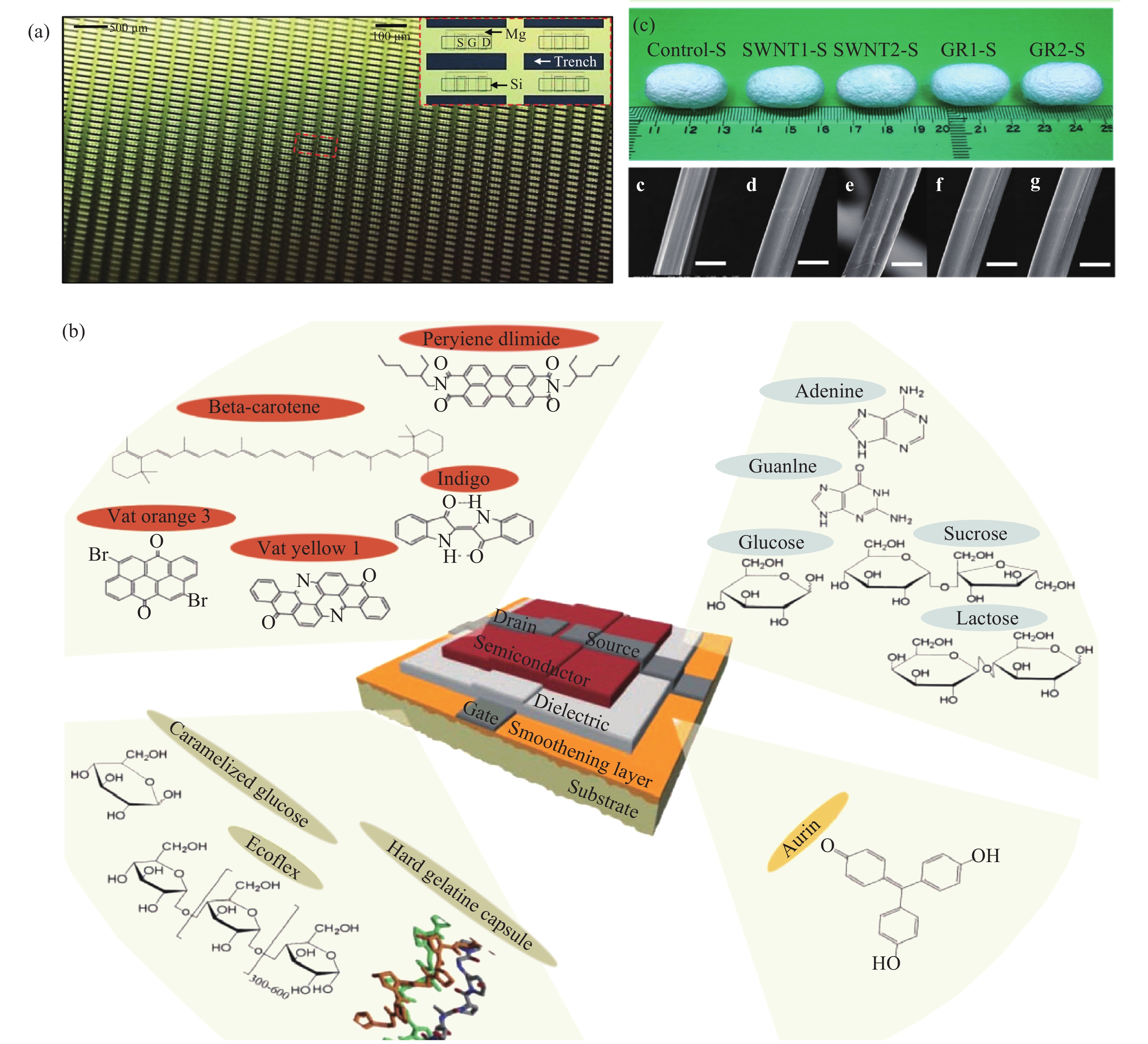
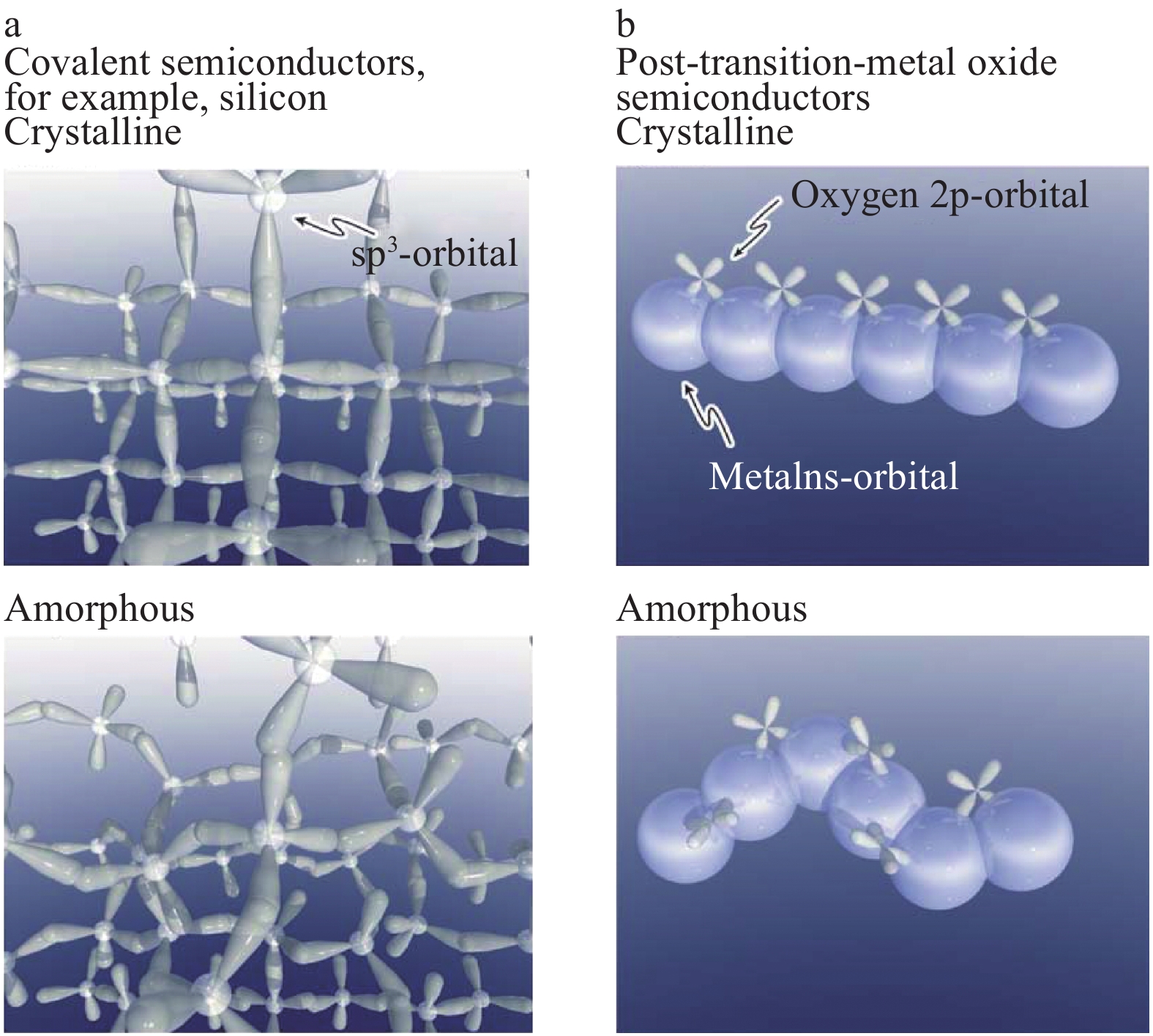
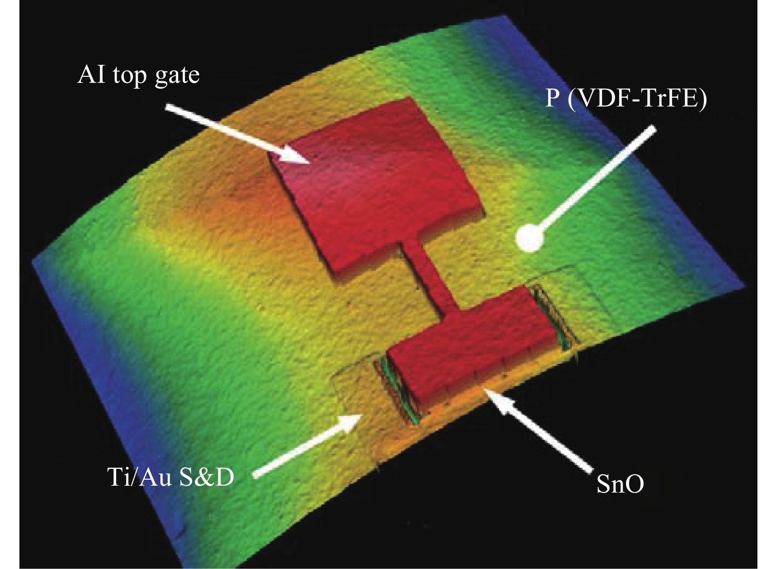
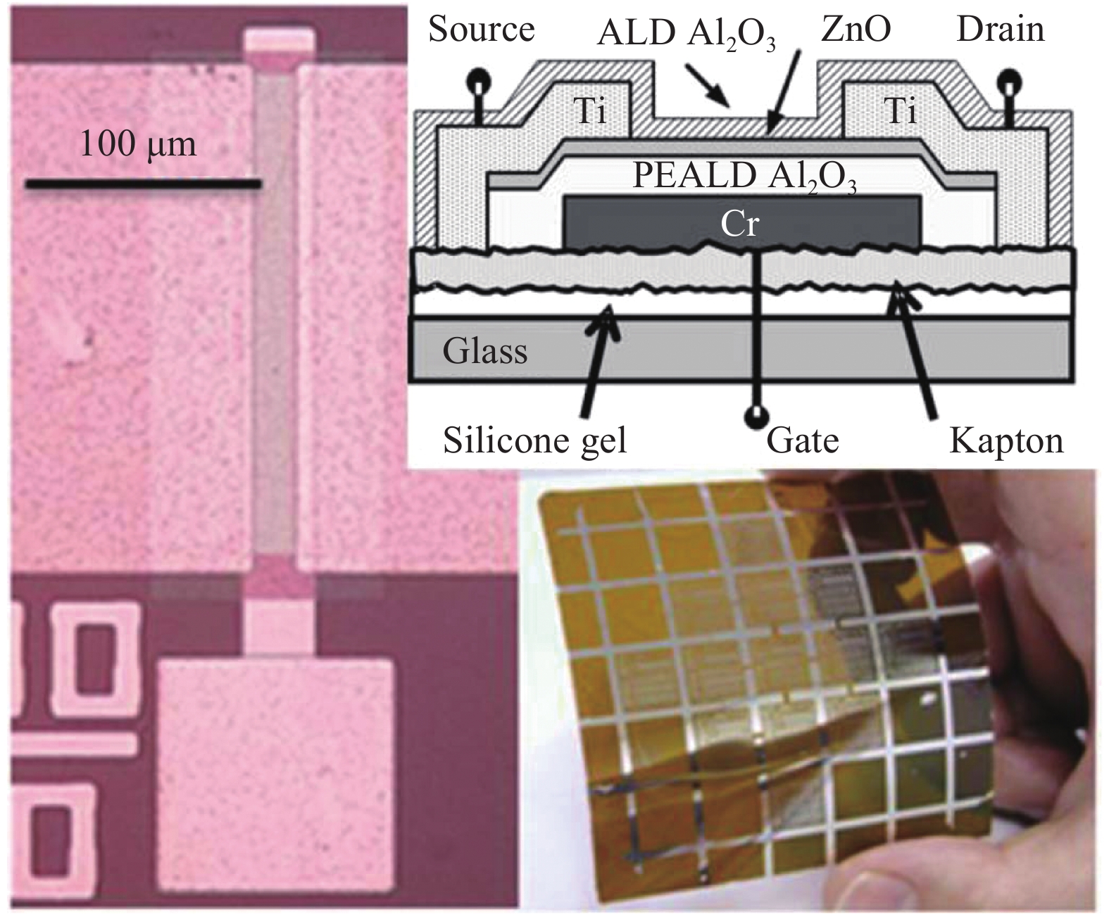
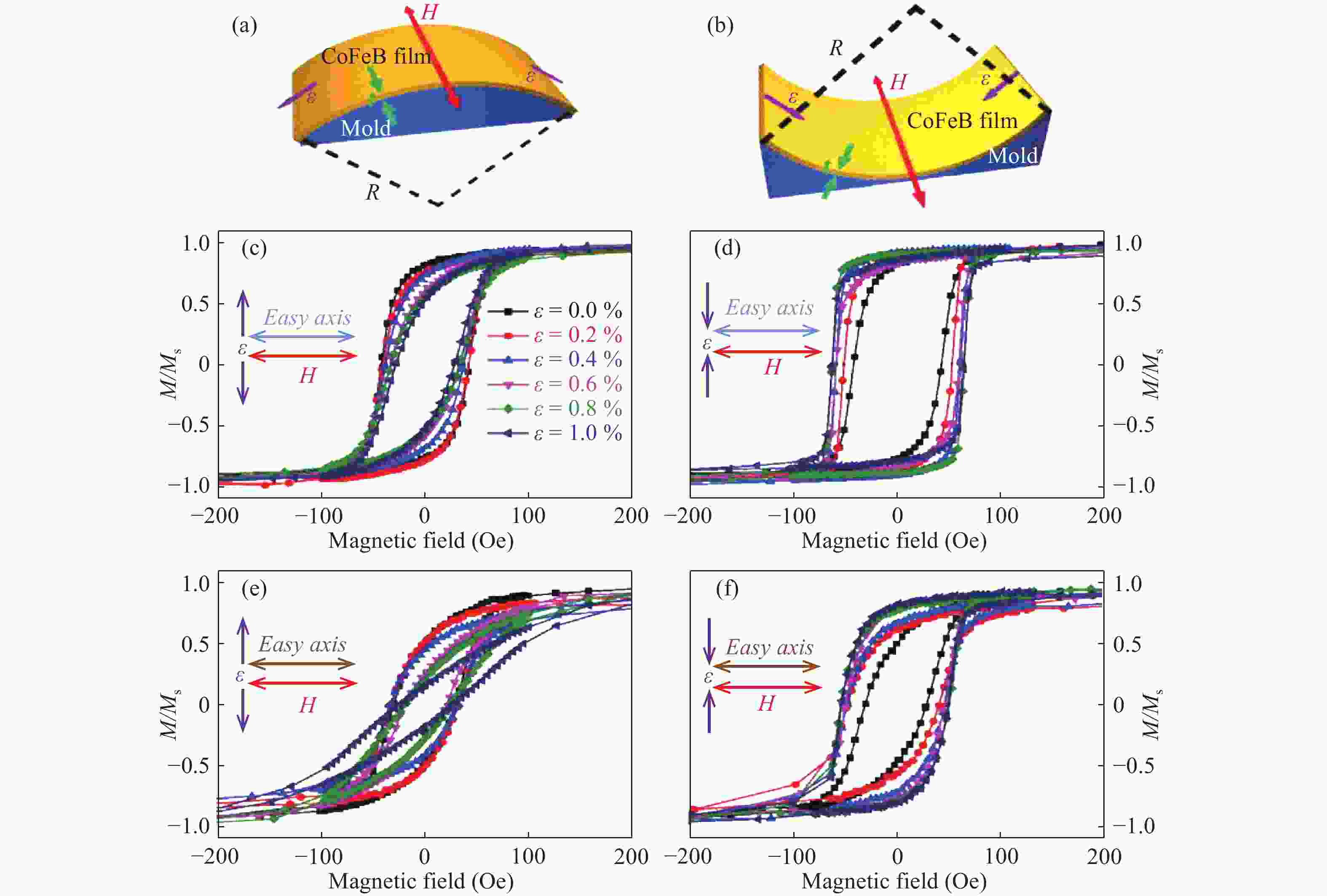
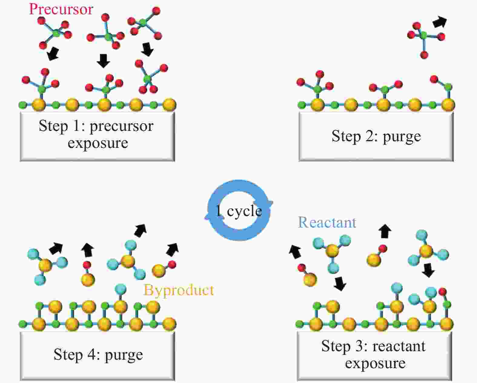
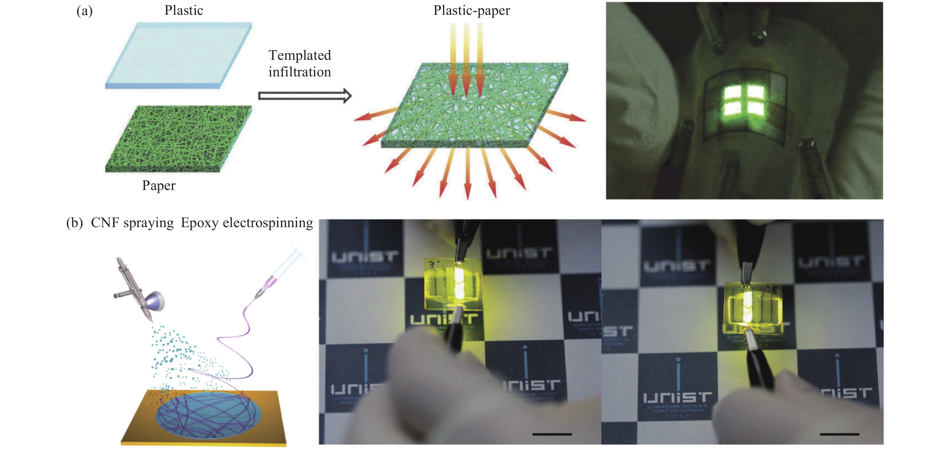
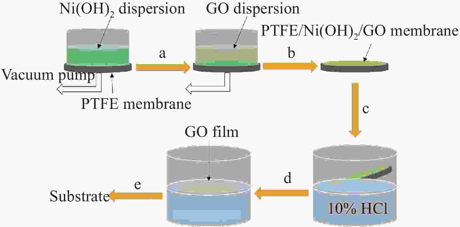
In this special issue, we organized a special issue on flexible and wearable electronics. Our aim is to highlight remarkable contributions made by the leading scientists in this important research area and broad impacts of flexible and wearable electronics. This special issue contains 12 review articles and 6 original research articles. One important issue include in this special issue collection is materials used for flexible/wearable electronics such as carbon nanomaterials, graphene, metal oxides, organic semiconductors, silicon, etc. Materials processing and flexible device fabrication techniques are also included in this special issue such as atomic layer deposition to metal oxides for thin-film transistors, printing techniques to flexible or stretchable circuits, etc. Another important issue includes in this issue is flexible electronic devices such as flexible sensors, textile energy storage devices and biosensors, flexible thin-film transistors, magnetic thin film devices, organic optoelectronic devices, stretchable human-machine interface, etc.
We sincerely hope that this special issue could provide a valuable reference and perspective for the research community working in this exciting field and inspire many more to enter this field. We would like to thank all the authors who have contributed high-quality peer-reviewed articles to this special issue. We are also grateful to the editorial and production staff of Journal of Semiconductors for their superb assistance.