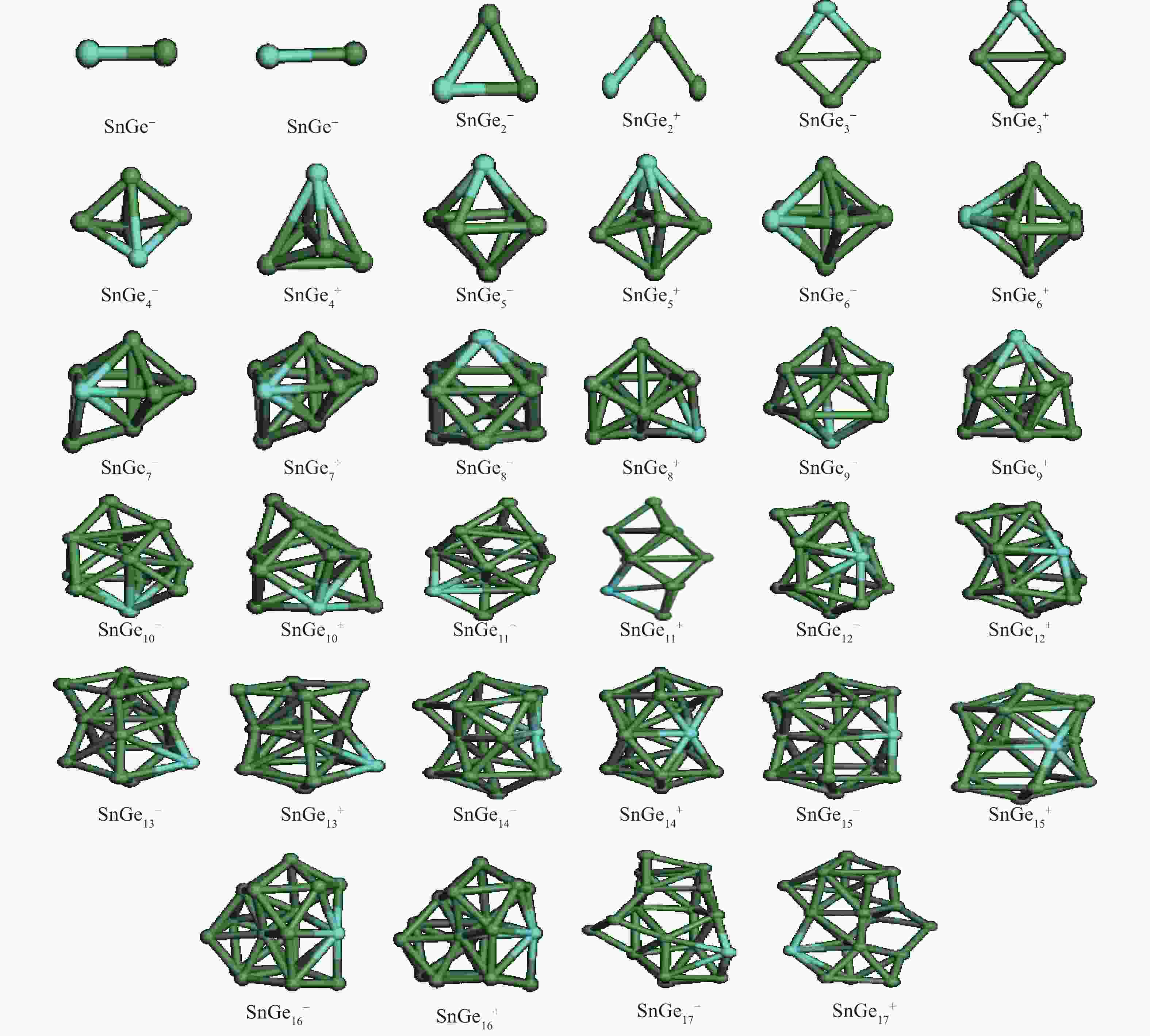
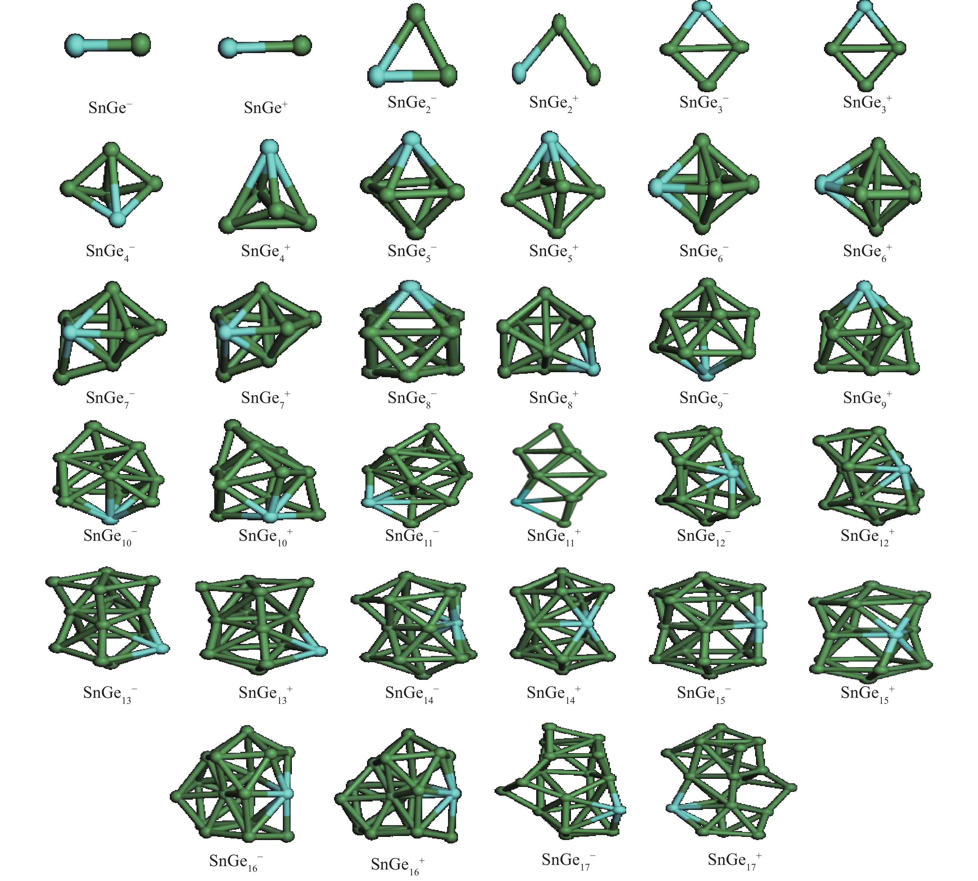
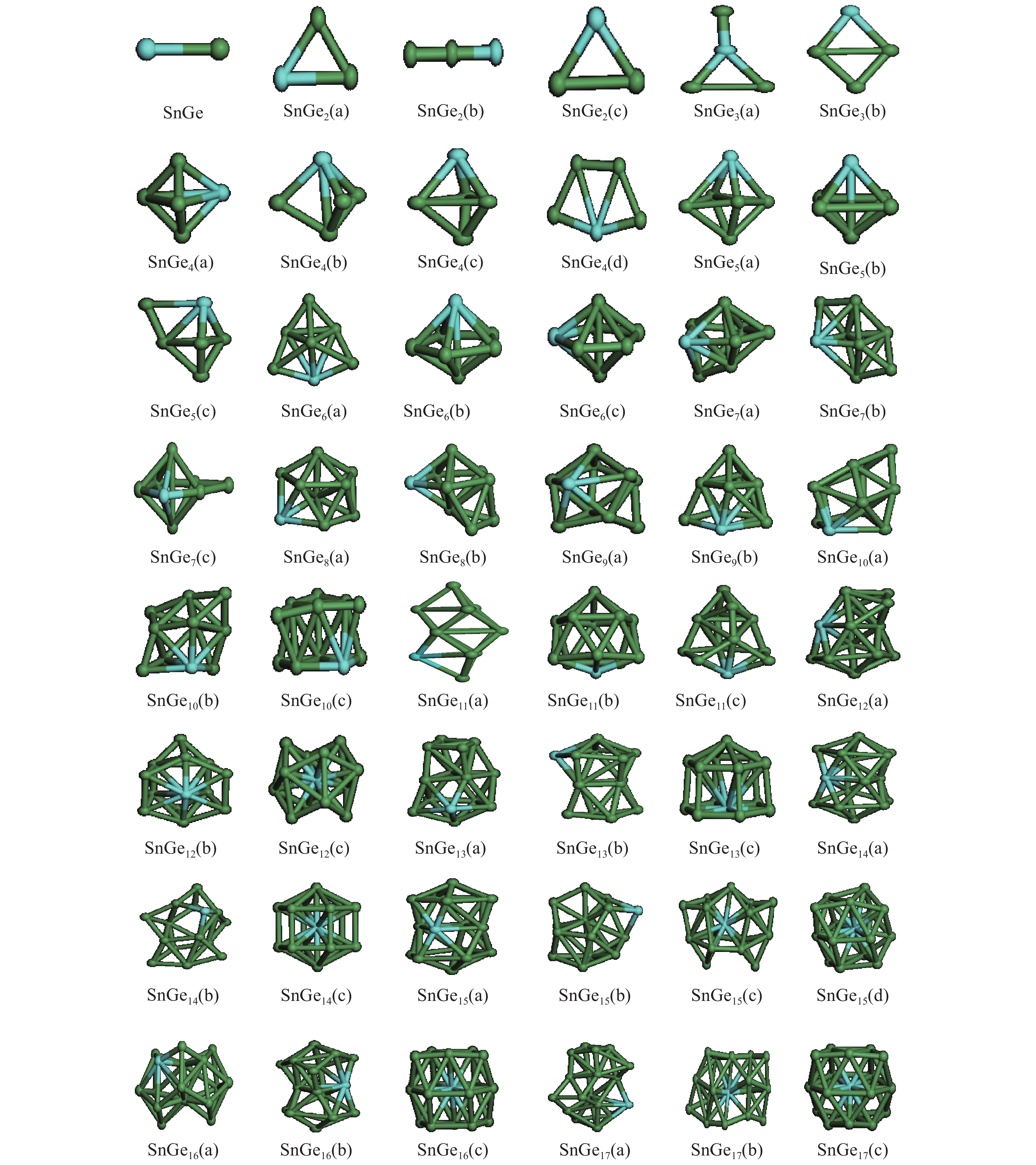
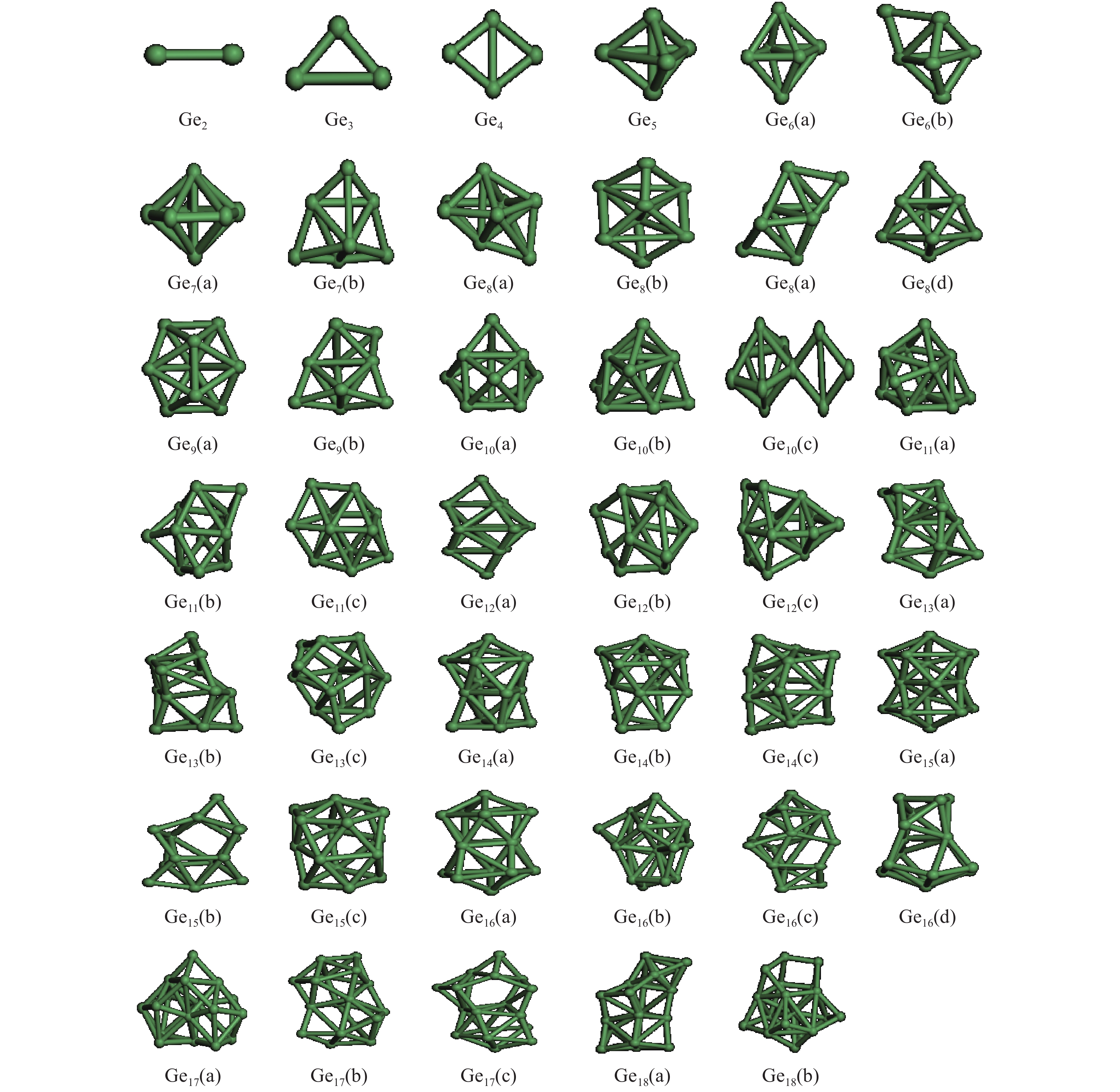
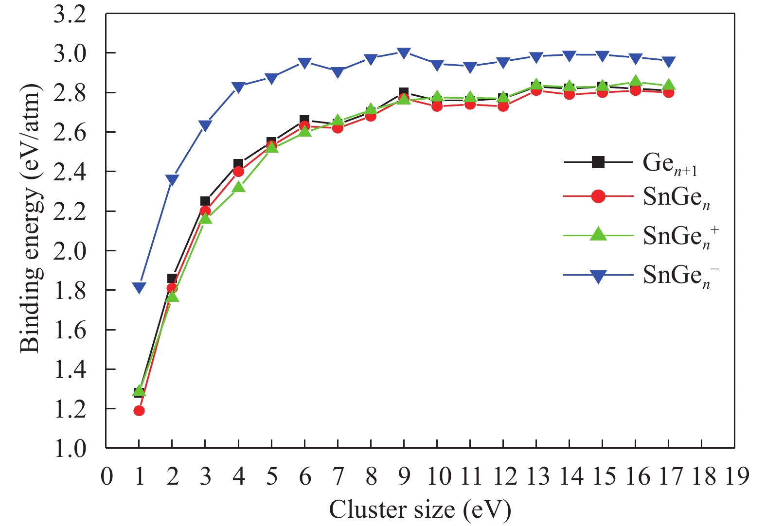
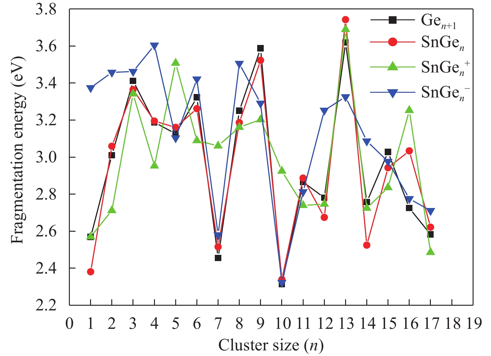
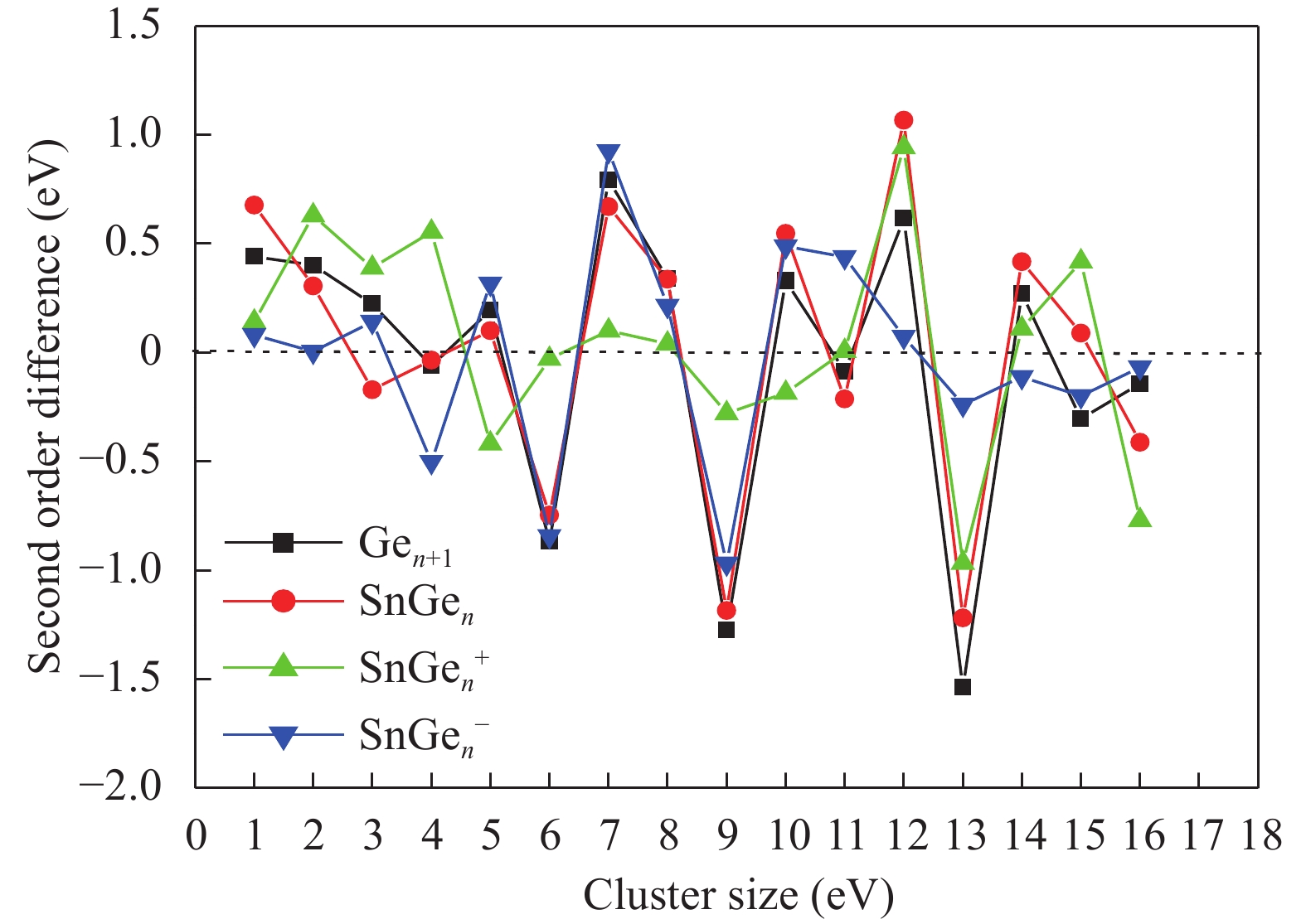
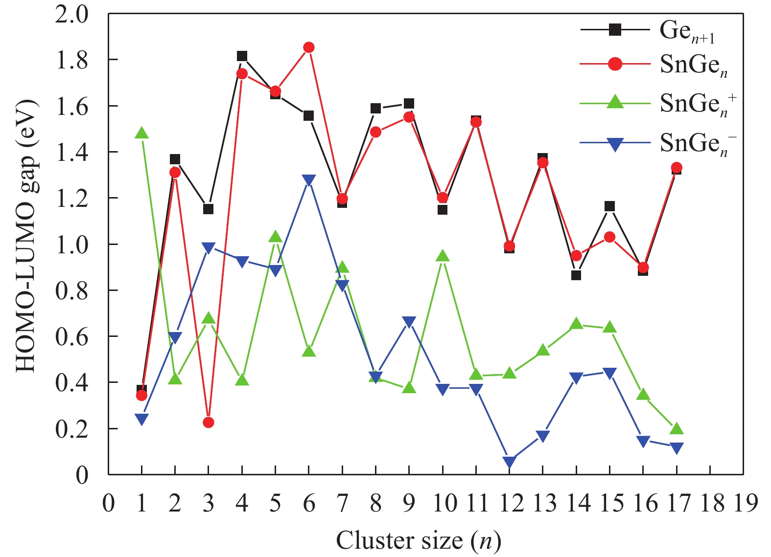
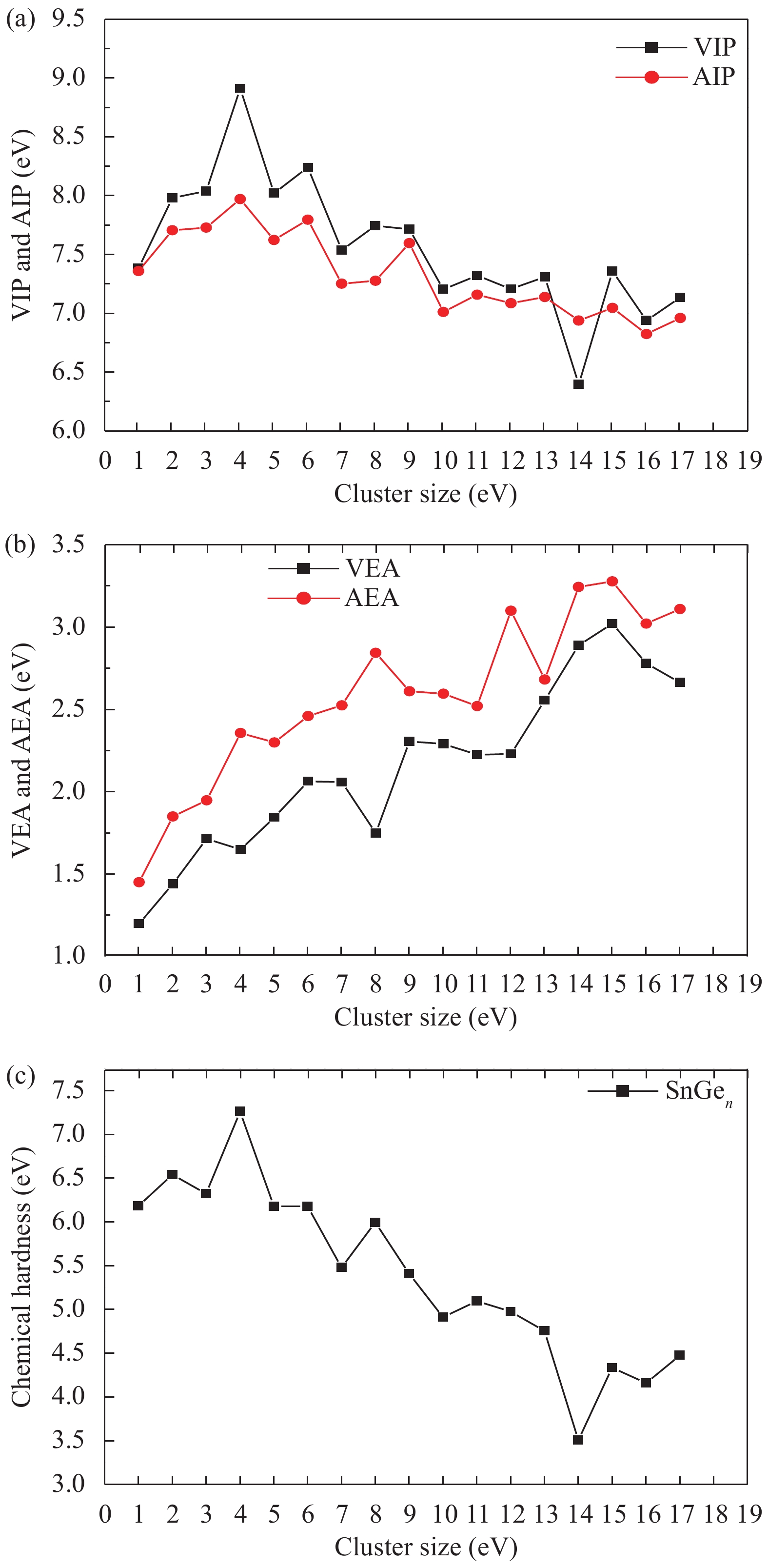
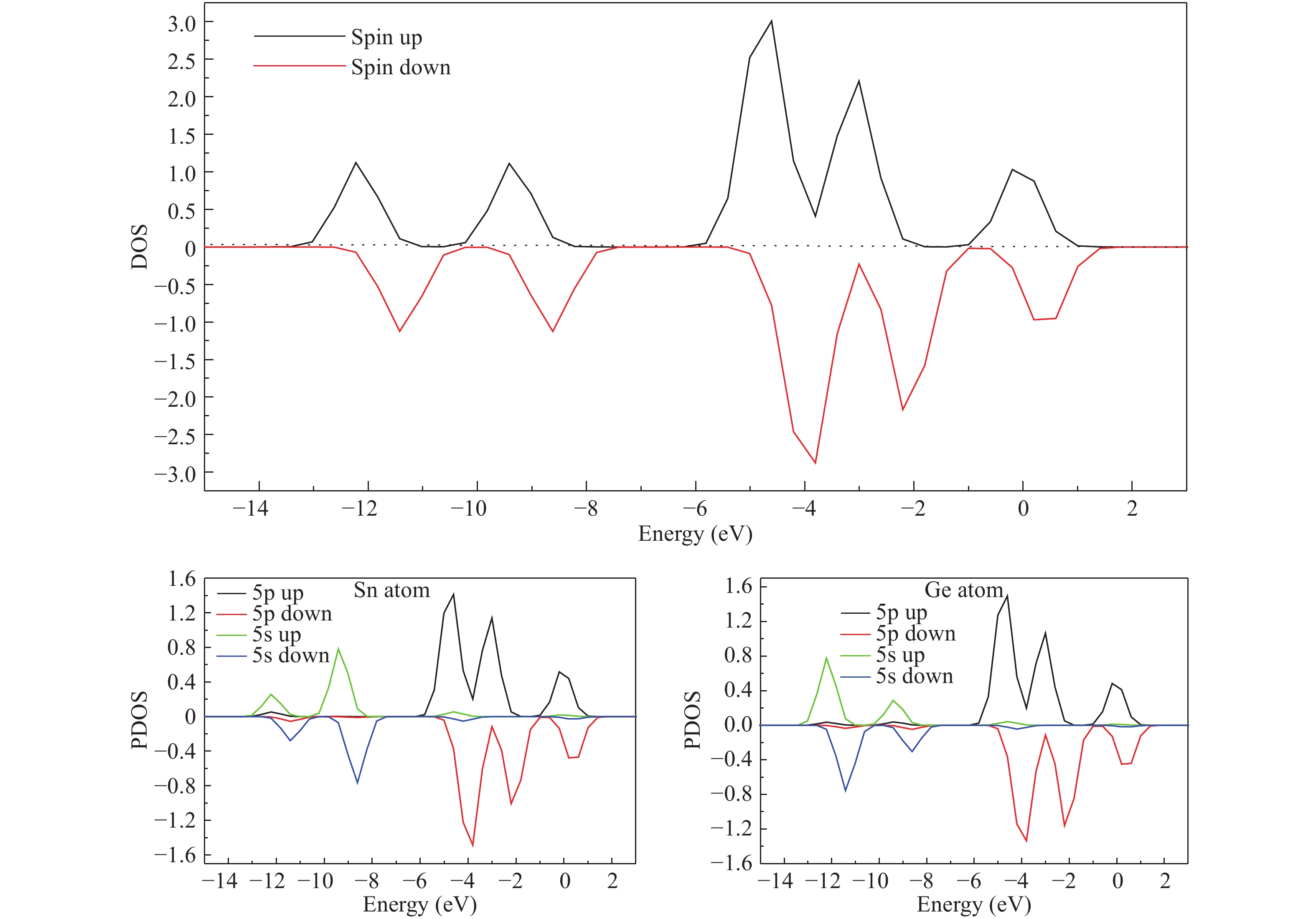
The structures, relative stability and magnetic properties of pure Gen+1, neutral cationic and anionic SnGen (n = 1–17) clusters have been investigated by using the first principles density functional theory implemented in SIESTA packages. We find that with the increasing of cluster size, the Gen+1 and SnGen(0, ±1) clusters tend to adopt compact structures. It has been also found that the Sn atom occupied a peripheral position for SnGen clusters when n < 12 and occupied a core position for n > 12. The structural and electronic properties such as optimized geometries, fragmentation energy, binding energy per atom, HOMO–LUMO gaps and second-order differences in energy of the pure Ge n+1 and SnGen clusters in their ground state are calculated and analyzed. All isomers of neutral SnGen clusters are generally nonmagnetic except for n = 1 and 4, where the total spin magnetic moments is 2μb. The total (DOS) and partial density of states of these clusters have been calculated to understand the origin of peculiar magnetic properties. The cluster size dependence of vertical ionization potentials, vertical electronic affinities, chemical hardness, adiabatic electron affinities and adiabatic ionization potentials have been calculated and discussed.

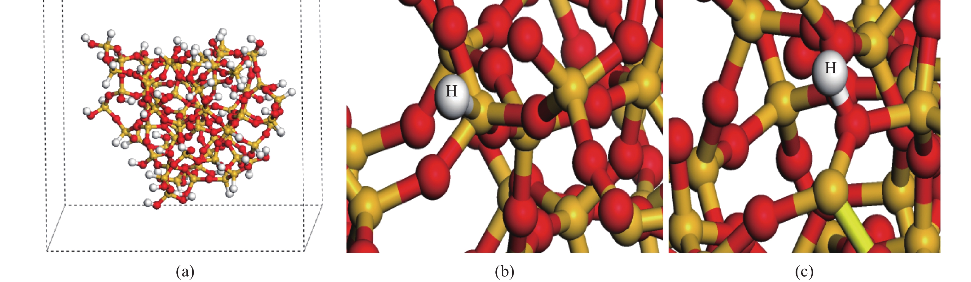
Hydrogen can be trapped in the bulk materials in four forms: interstitial molecular H2, interstitial atom H, O−H+(2Si=O–H)+, Si−H−(


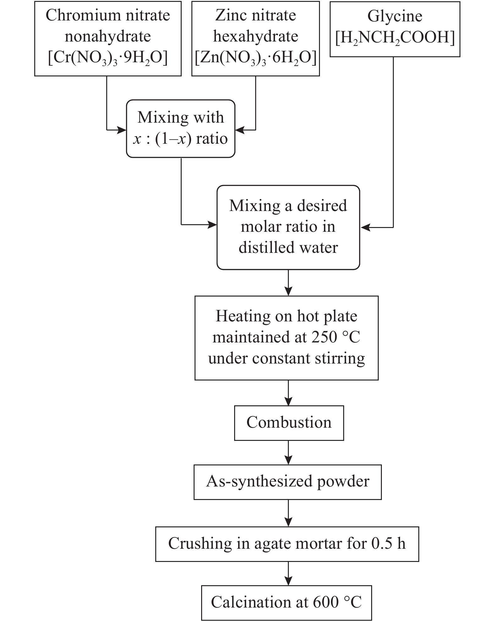
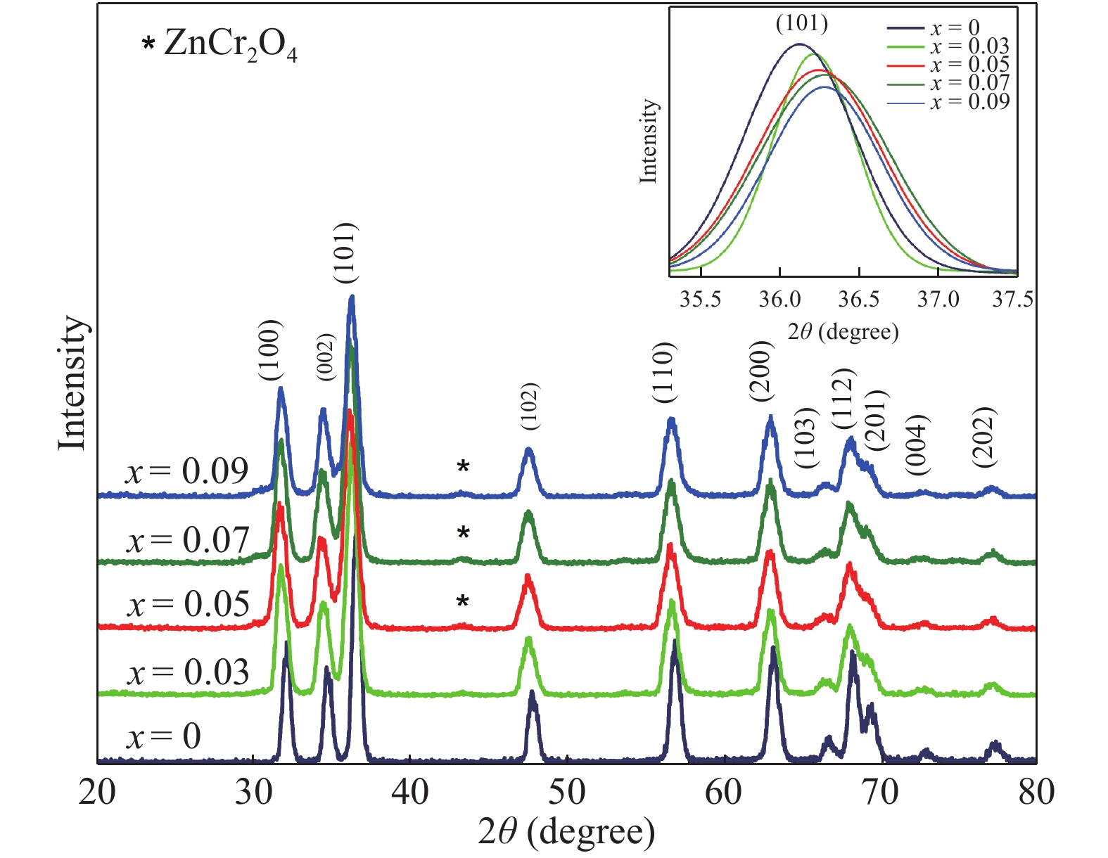
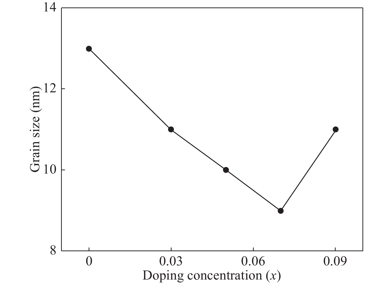
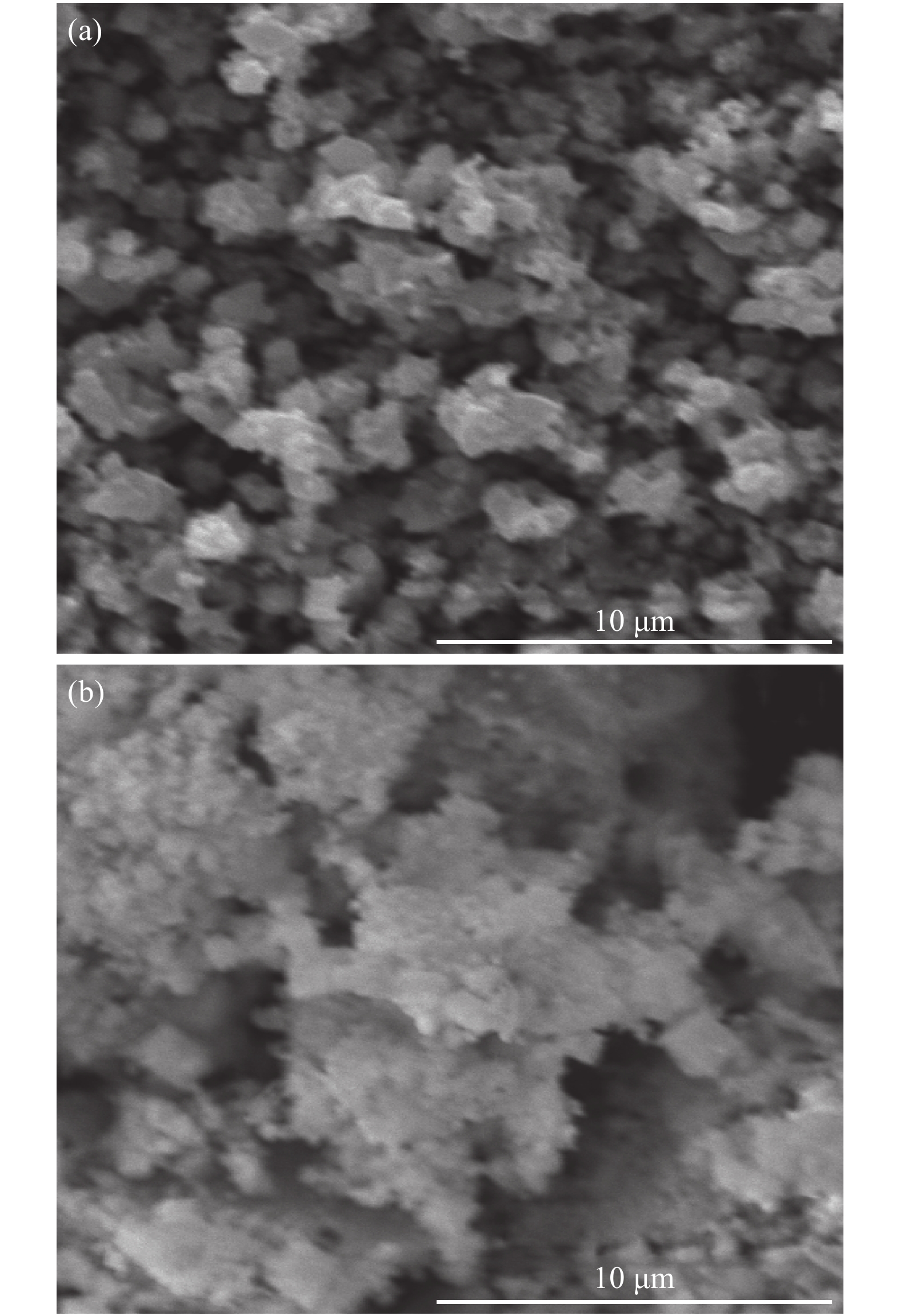
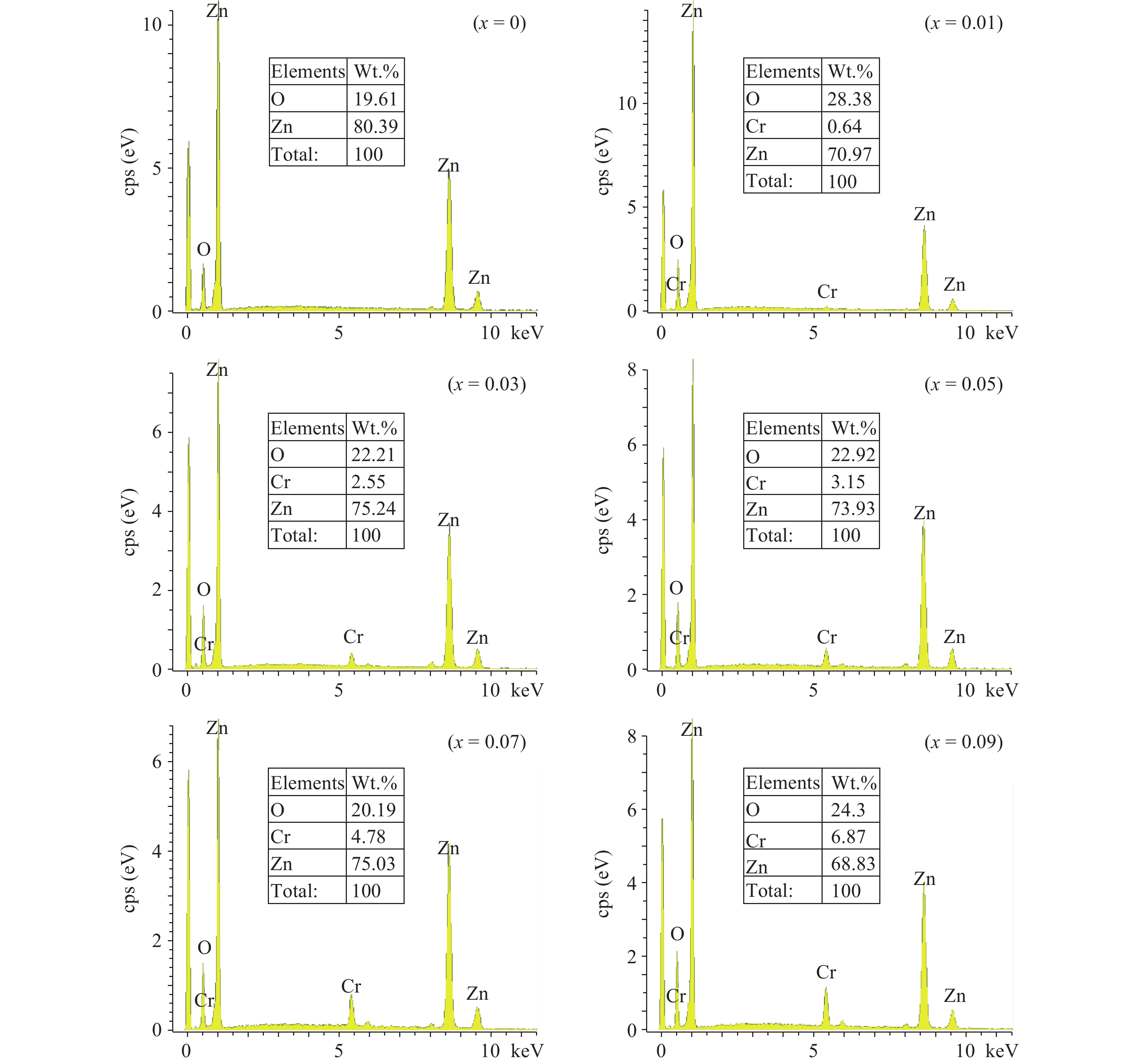
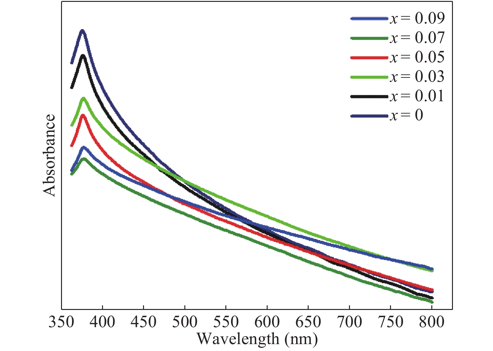
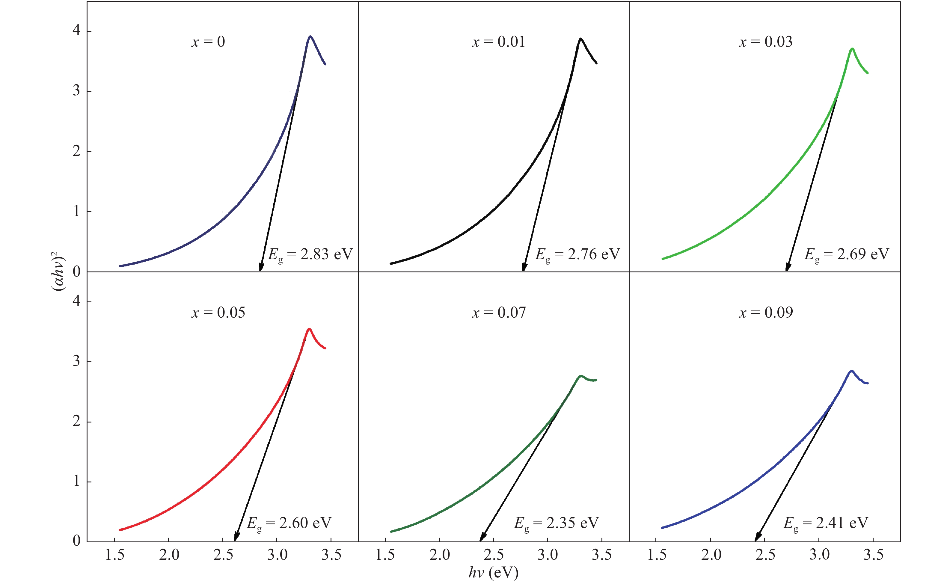
Zn1−xCrxO (x = 0.00, 0.01, 0.03, 0.05, 0.07, and 0.09) nanoparticles were synthesized, by an auto-combustion method. Structural, optical, and magnetic characteristics of Cr-doped ZnO samples calcined at 600 °C have been analyzed by using X-ray diffraction (XRD), field emission scanning electron microscope (FESEM), UV–Vis spectroscopy and vibrating sample magnetometer (VSM). The XRD data confirmed the hexagonal wurtzite structure of pure and Cr-doped ZnO nanoparticles. The calculated values of grain size using Scherrer's formula are in the range of 30.7–9.2 nm. The morphology of nanopowders has been observed by FESEM, and EDS results confirmed a systematic increase of Cr content in the samples and clearly indicate with no impurity element. The band gaps, computed by UV–Vis spectroscopy, are in the range of 2.83–2.35 eV for different doping concentrations. By analyzing VSM data, significantly enhanced room temperature ferromagnetism is identified in Cr-doped ZnO samples. The value of magnetization is a 12 times increased of the value reported by Daunet al. (2010). Room temperature ferromagnetism of the nanoparticles is of vital prominence for spintronics applications.

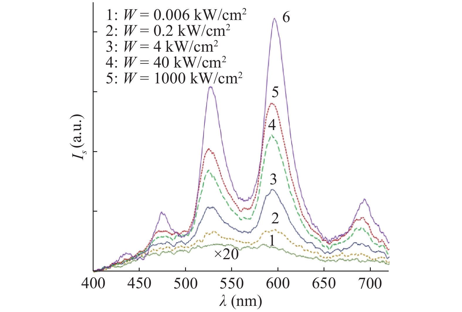
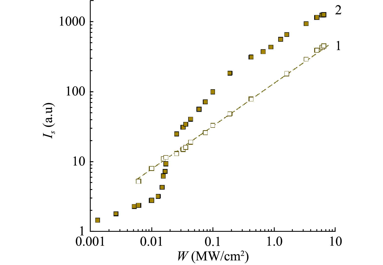
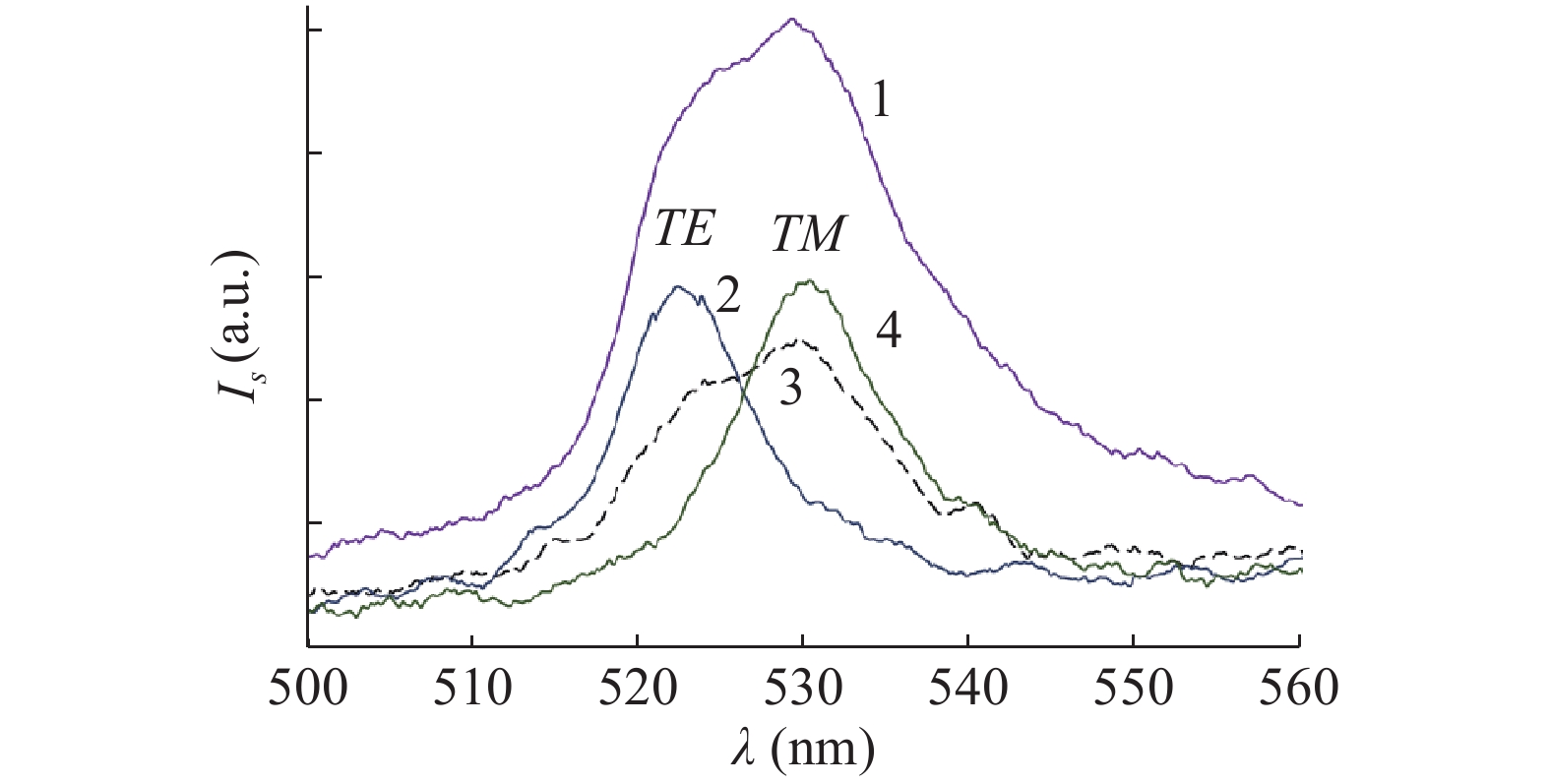
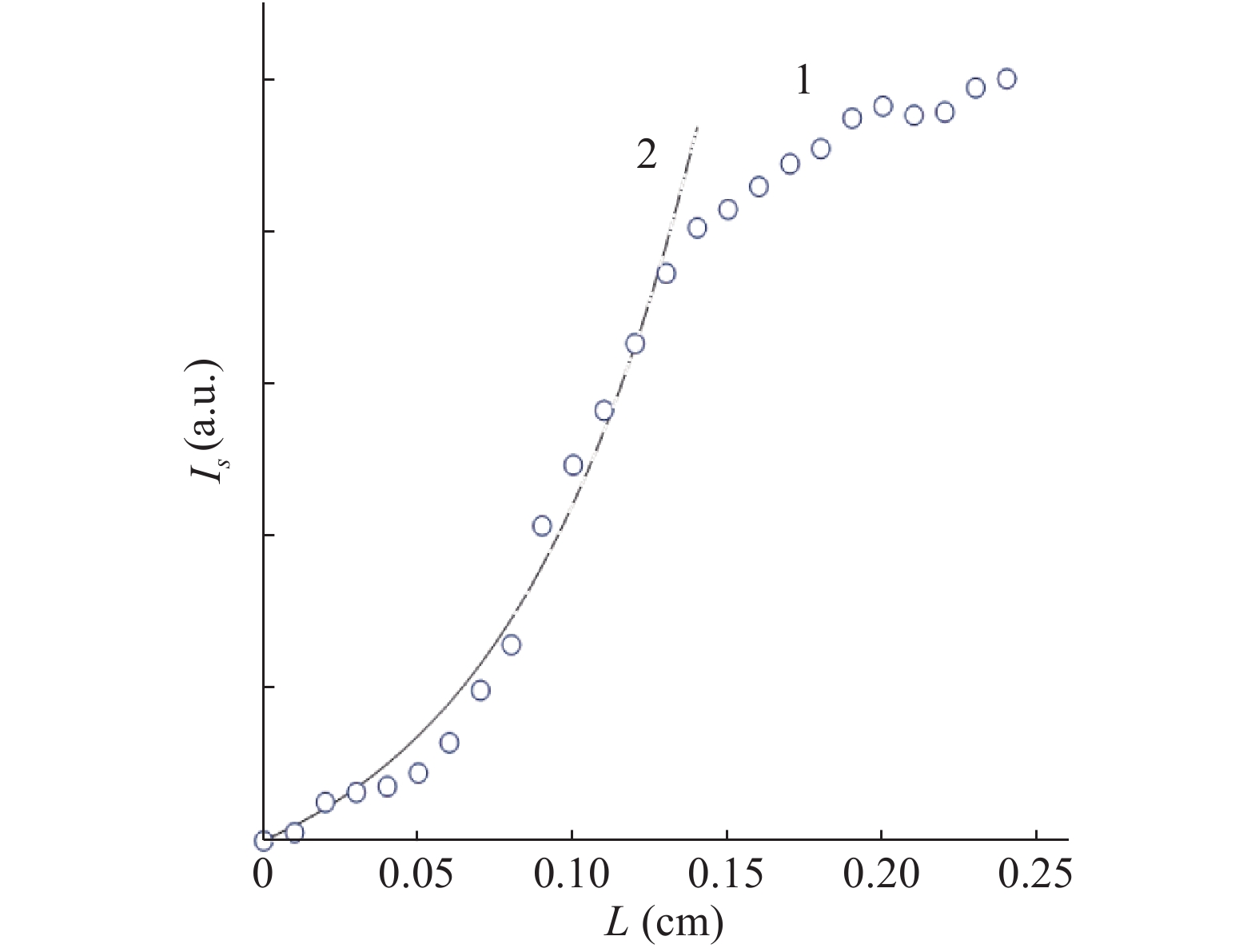
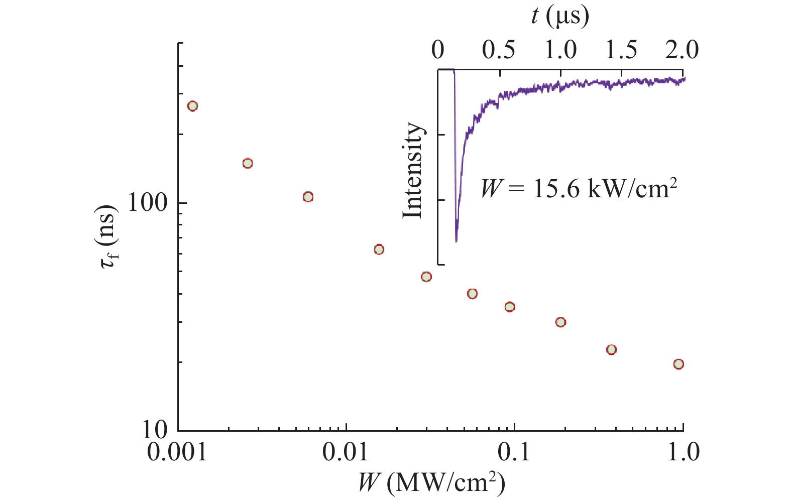
Spectral, temporal and polarization characteristics of spontaneous and stimulated luminescence of Al0.5Ga0.5N/AlN structures grown by molecular beam epitaxy were studied at the optical pulsed pumping with λ = 266 nm. Samples with a high degree of silicon doping were investigated. The vast majority of radiation falls on transitions within the band gap between the levels of defects. As a result, the radiation band embracing the whole visible range of more than 300 THz is observed in both spontaneous radiation and induced luminescence. In spontaneous radiation the band has a smooth spectral intensity distribution over the wavelengths, whereas induced radiation has its sharp peaks corresponding to the mode structure of the planar waveguide. The measured gain of the active medium is g ≈ 70 cm−1 for a weak signal.


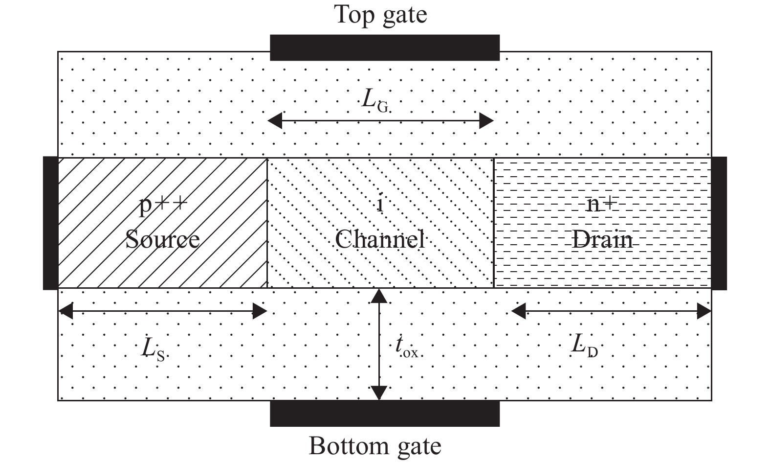
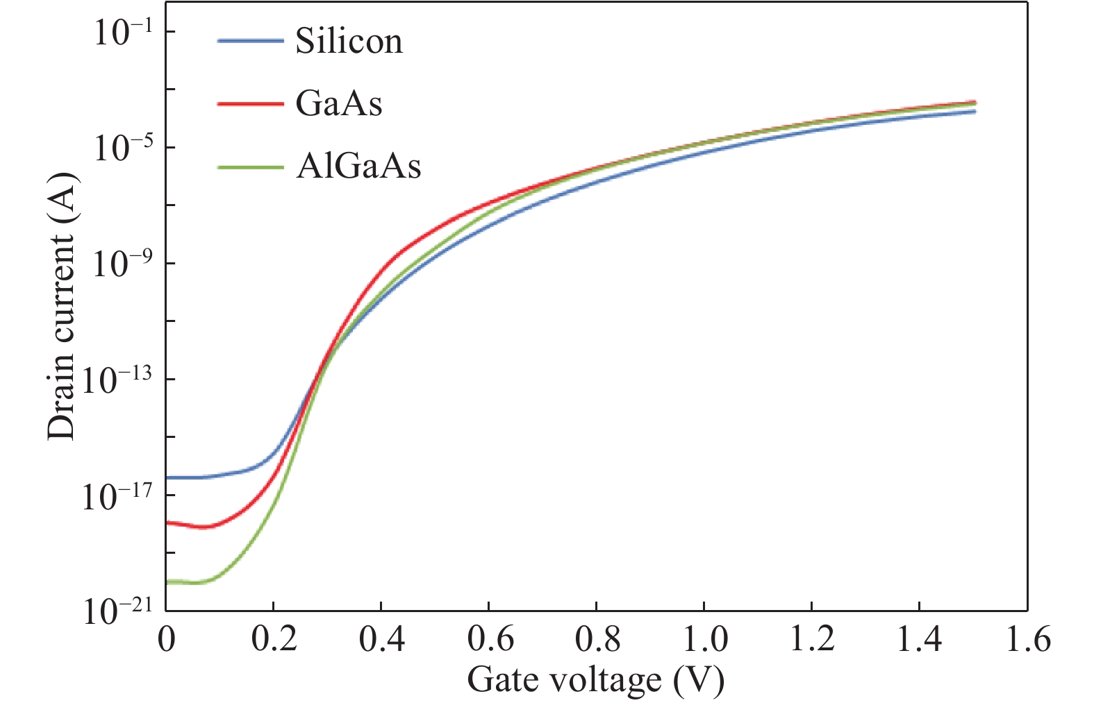
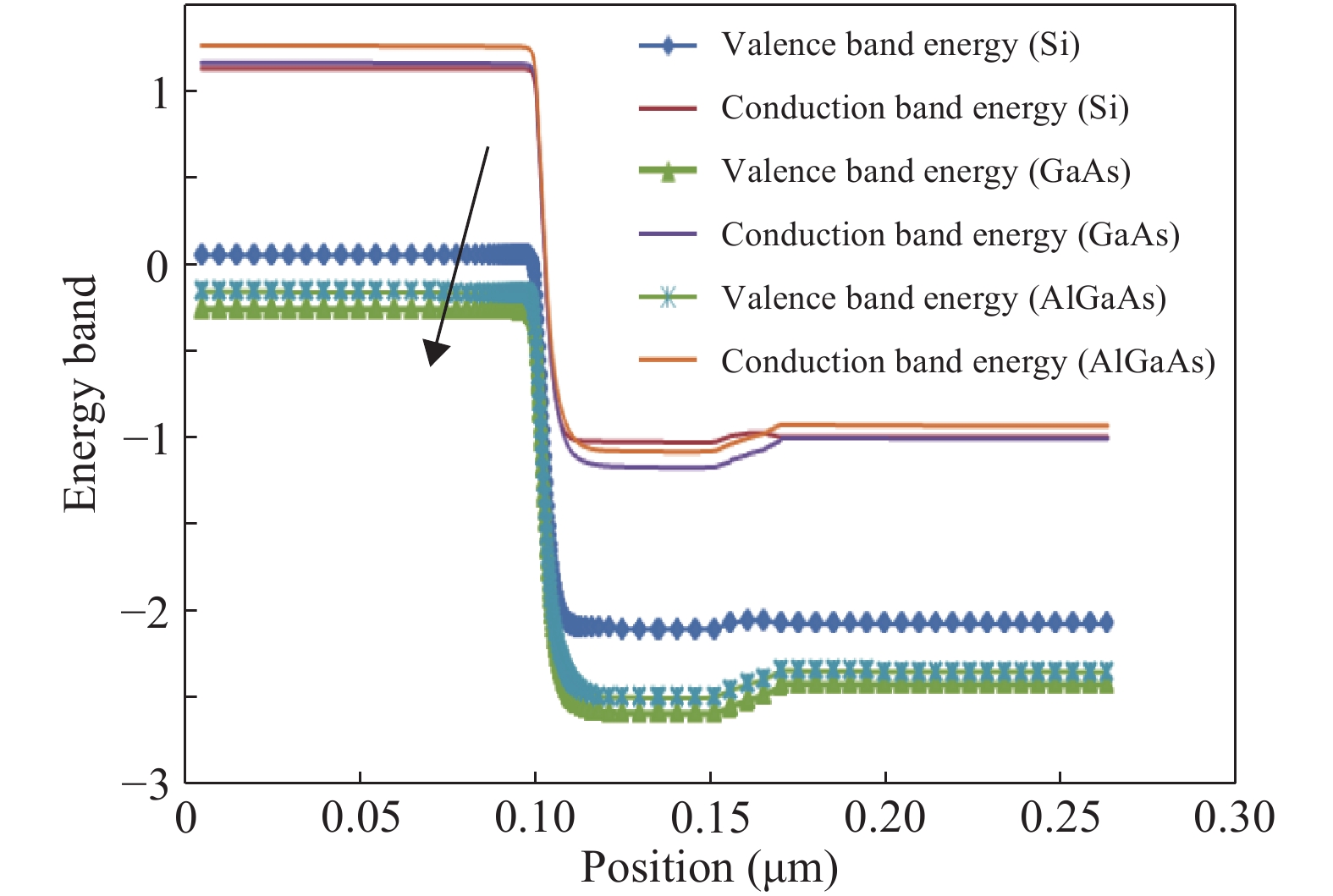
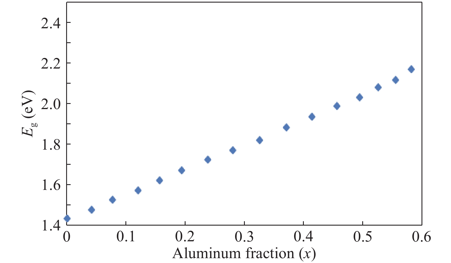
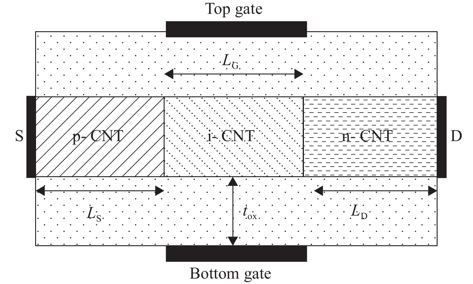
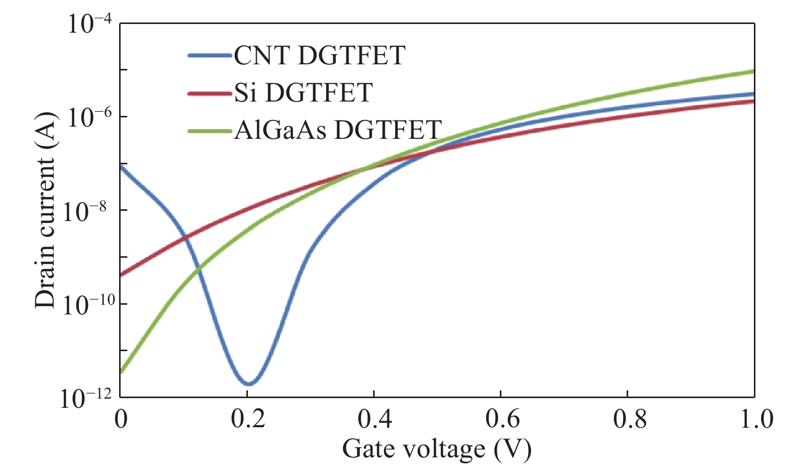
A double-gate tunnel field-effect transistor (DG tunnel FET) has been designed and investigated for various channel materials such as silicon (Si), gallium arsenide (GaAs), alminium gallium arsenide (AlxGa1−xAs) and CNT using a nano ViDES Device and TCAD SILVACO ATLAS simulator. The proposed devices are compared on the basis of inverse subthreshold slope (SS), ION/IOFF current ratio and leakage current. Using Si as the channel material limits the property to reduce leakage current with scaling of channel, whereas the AlxGa1−xAs based DG tunnel FET provides a better ION/IOFF current ratio (2.51 × 10⁶) as compared to other devices keeping the leakage current within permissible limits. The performed silmulation of the CNT based channel in the double-gate tunnel field-effect transistor using the nano ViDES shows better performace for a sub-threshold slope of 29.4 mV/dec as the channel is scaled down. The proposed work shows the potential of the CNT channel based DG tunnel FET as a futuristic device for better switching and high retention time, which makes it suitable for memory based circuits.


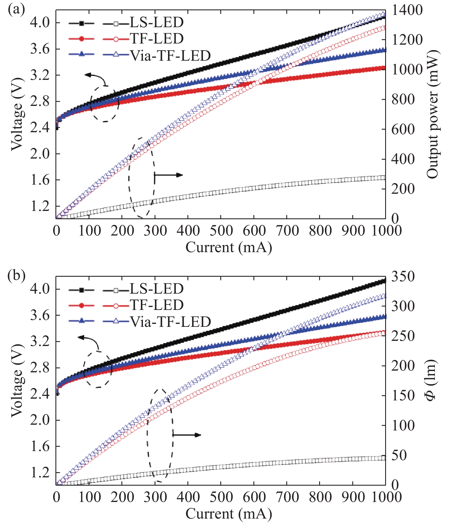
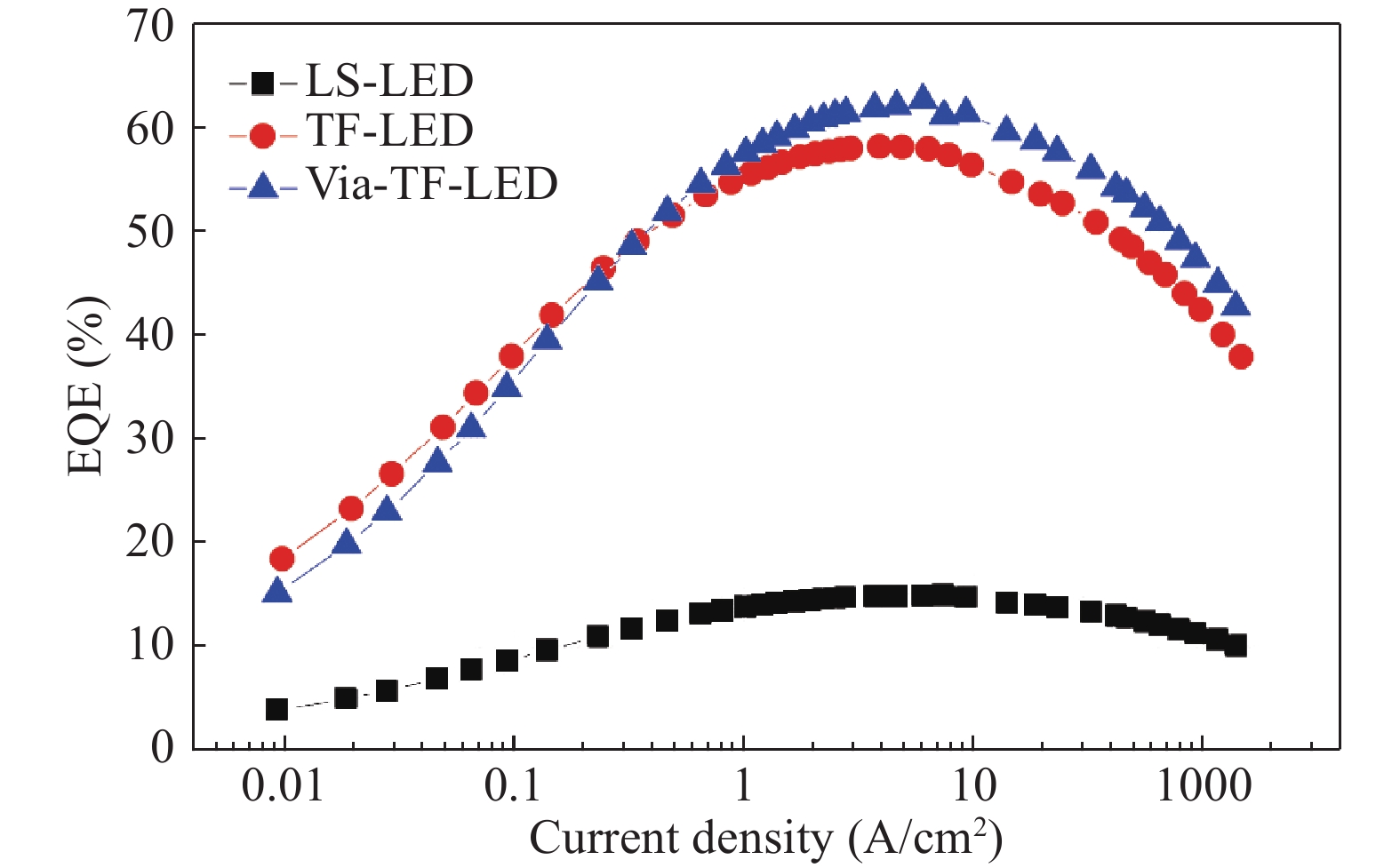
This work reports the fabrication of via-thin-film light-emitting diode (via-TF-LED) to improve the light output power (LOP) of blue/white GaN-based LEDs grown on Si (111) substrates. The as-fabricated via-TF-LEDs were featured with a roughened n-GaN surface and the p-GaN surface bonded to a wafer carrier with a silver-based reflective electrode, together with an array of embedded n-type via pillar metal contact from the p-GaN surface etched through the multiple-quantum-wells (MQWs) into the n-GaN layer. When operated at 350 mA, the via-TF-LED gave an enhanced blue LOP by 7.8% and over 3.5 times as compared to the vertical thin-film LED (TF-LED) and the conventional lateral structure LED (LS-LED). After covering with yellow phosphor that converts some blue photons into yellow light, the via-TF-LED emitted an enhanced white luminous flux by 13.5% and over 5 times, as compared with the white TF-LED and the white LS-LED, respectively. The significant LOP improvement of the via-TF-LED was attributed to the elimination of light absorption by the Si (111) epitaxial substrate and the finger-like n-electrodes on the roughened emitting surface.

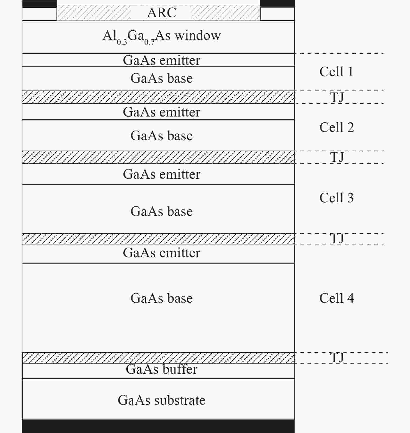
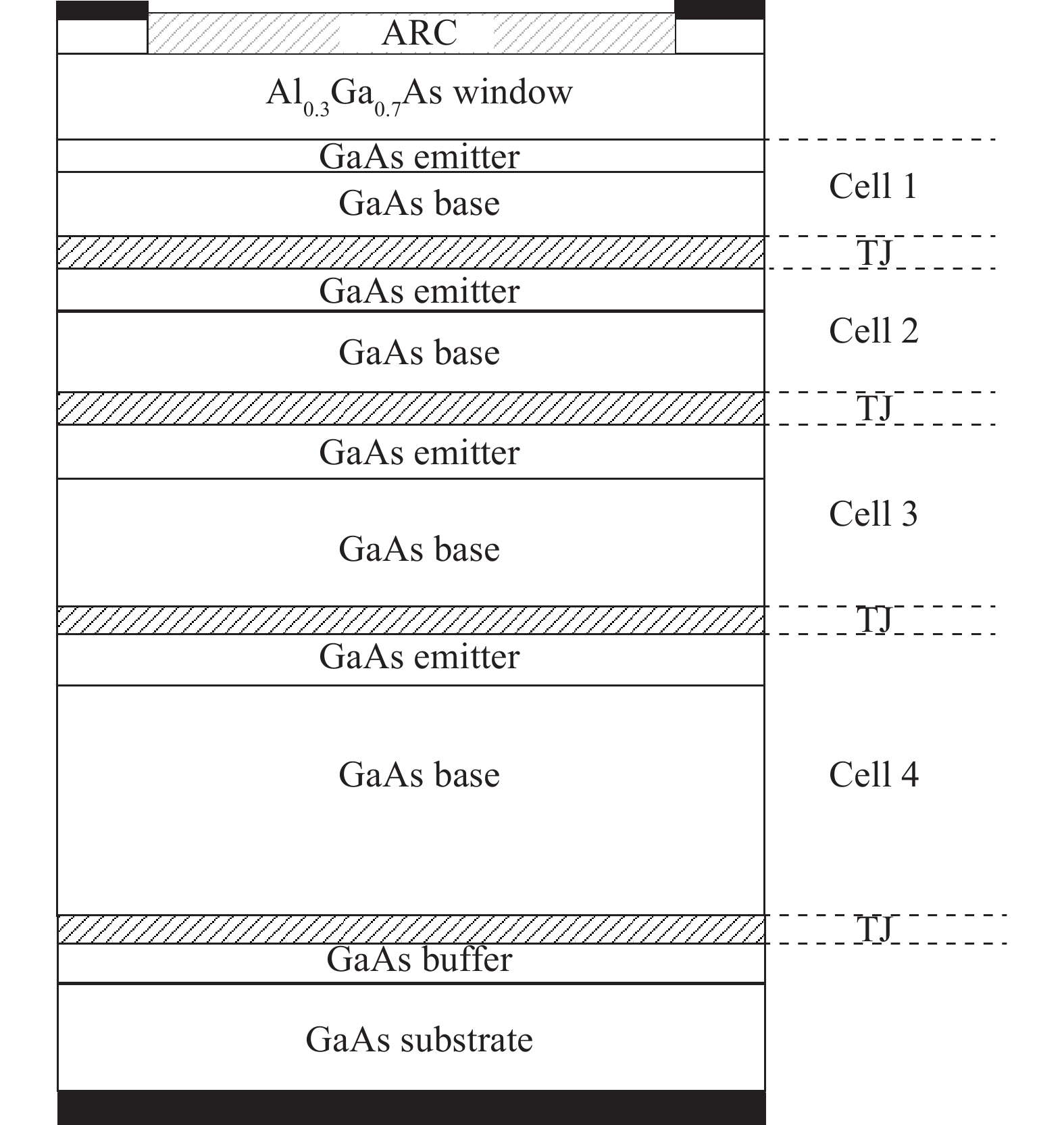
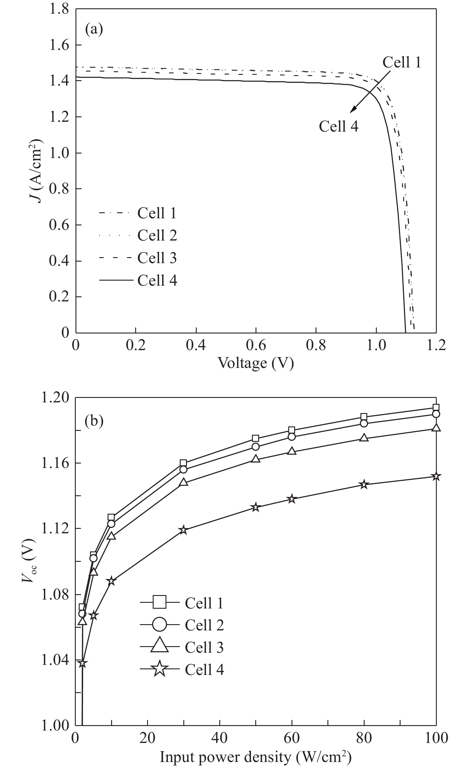
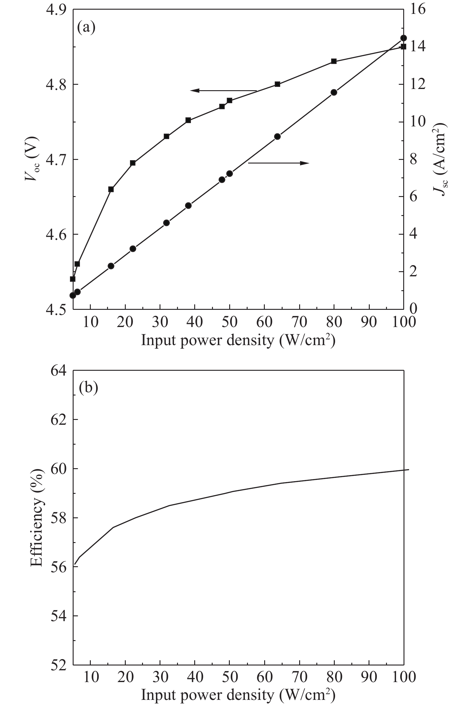
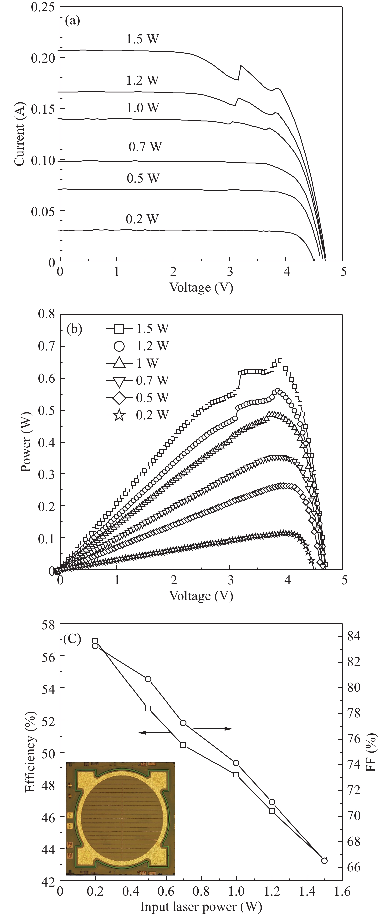
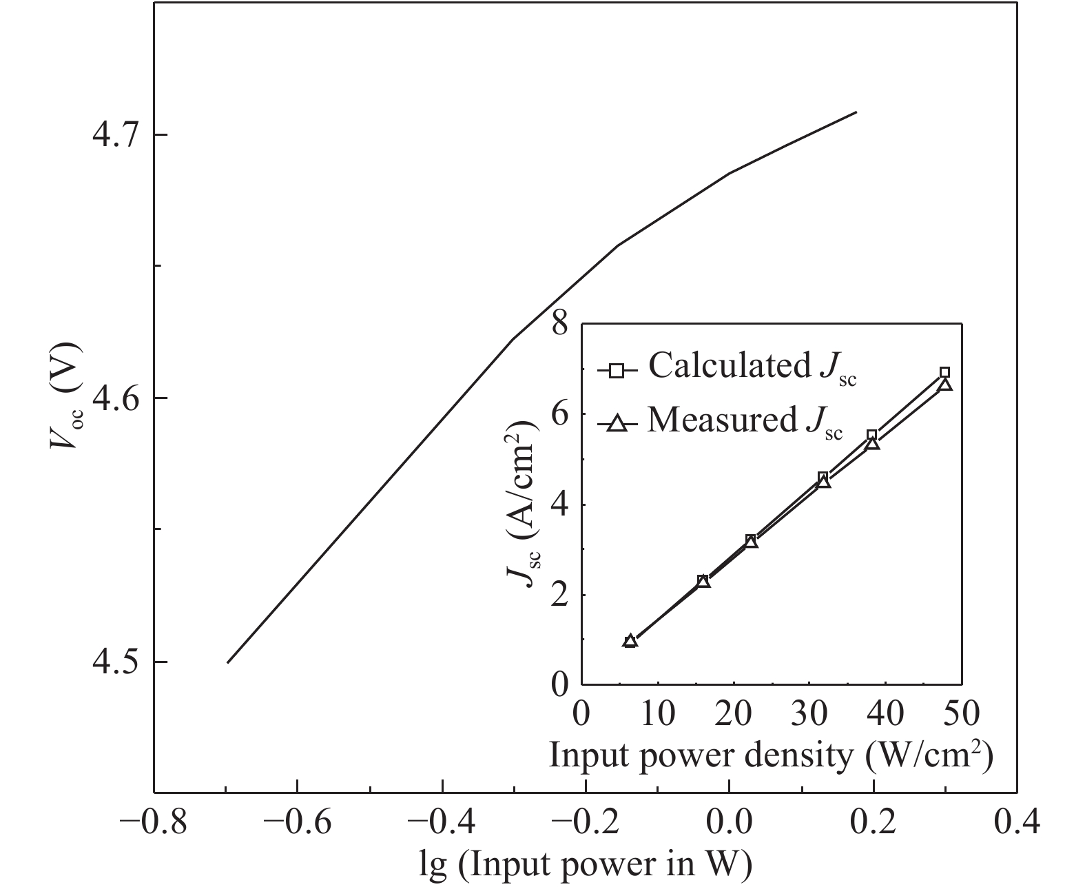
Four-junction AlGaAs/GaAs laser power converters (LPCs) with n+-GaAs/p+-Al0.37Ga0.63As heterostructure tunnel junctions (TJs) have been designed and grown by metal-organic chemical vapor deposition (MOCVD) for converting the power of 808 nm lasers. A maximum conversion efficiency ηc of 56.9% ± 4% is obtained for cells with an aperture of 3.14 mm2 at an input laser power of 0.2 W, while dropping to 43.3% at 1.5 W. Measured current–voltage (I–V) characteristics indicate that the performance of the LPC can be further improved by increasing the tunneling current density of TJs and optimizing the thicknesses of sub-cells to achieve current matching in LPC.
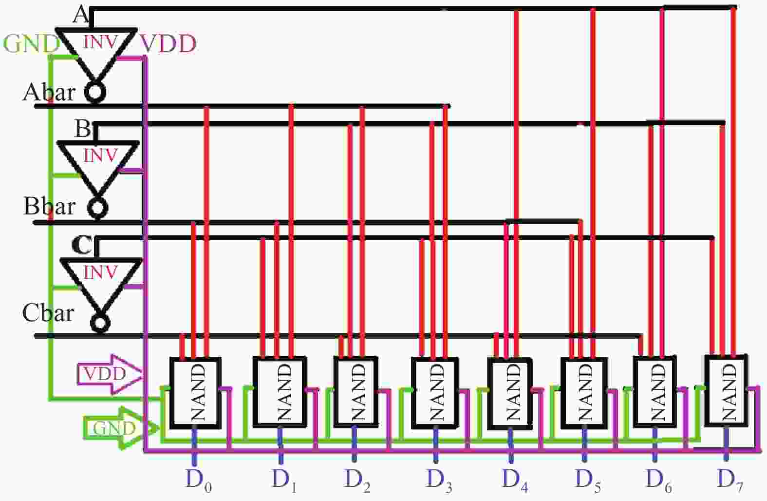
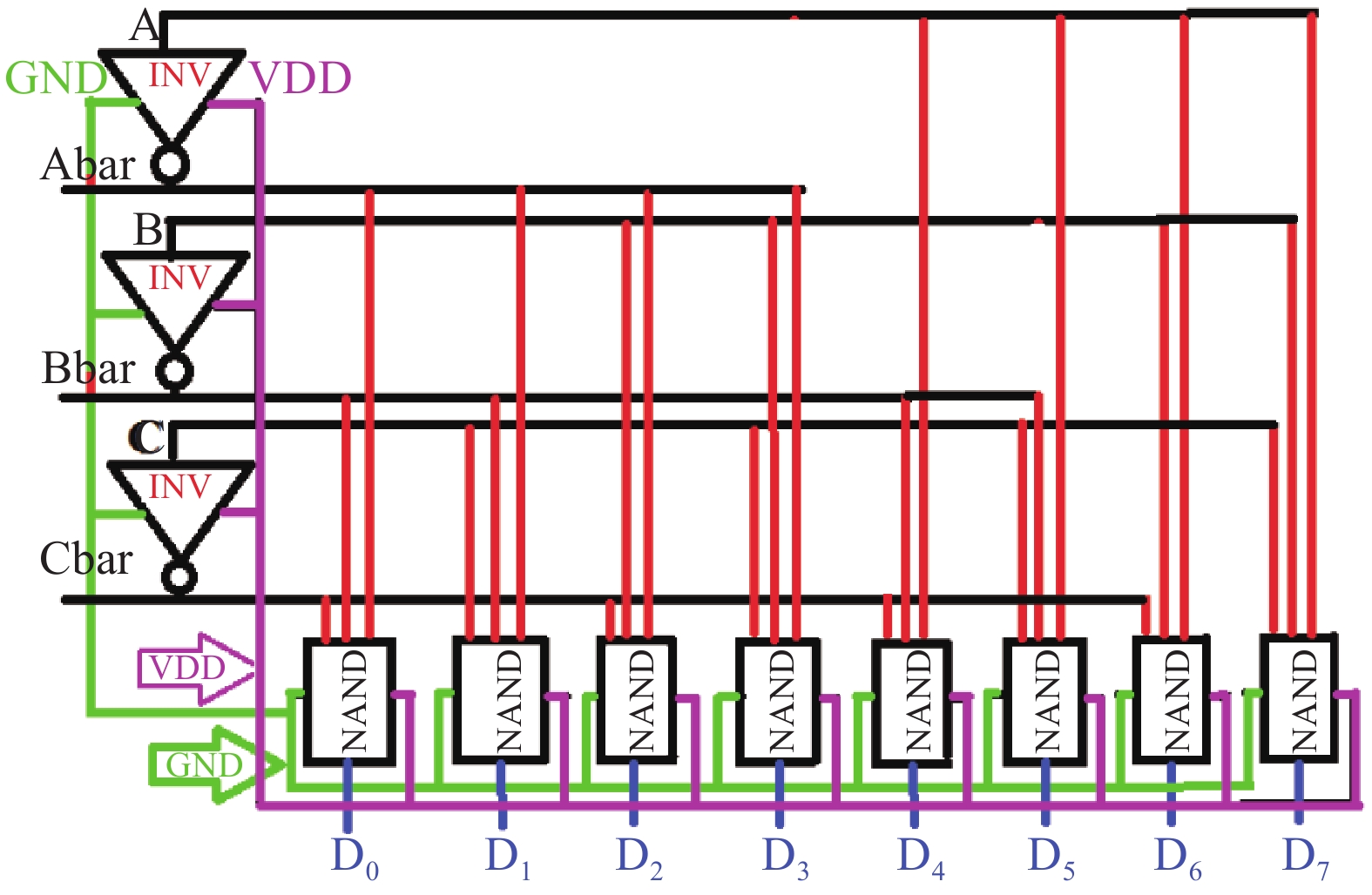
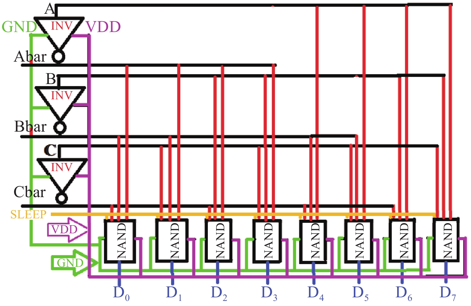
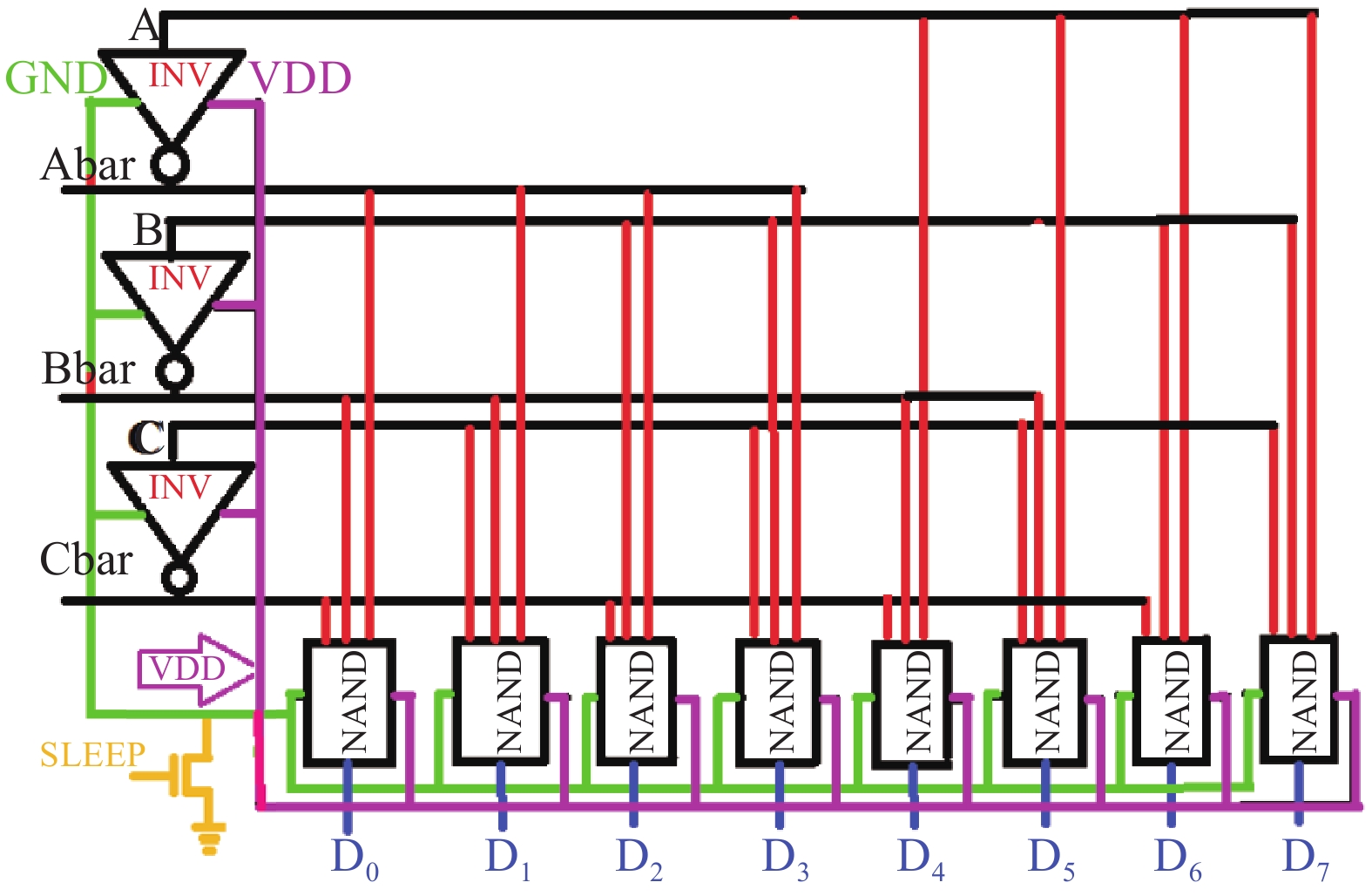
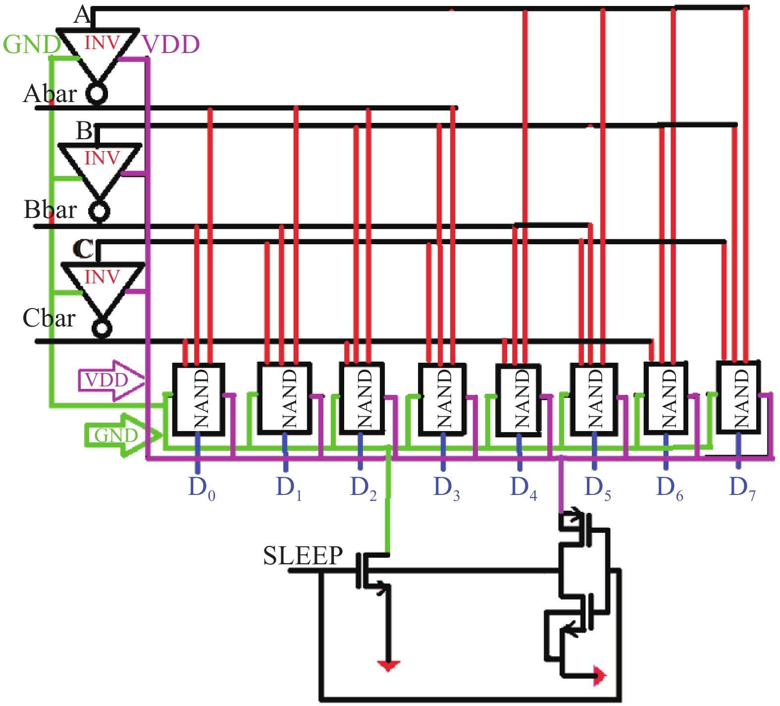
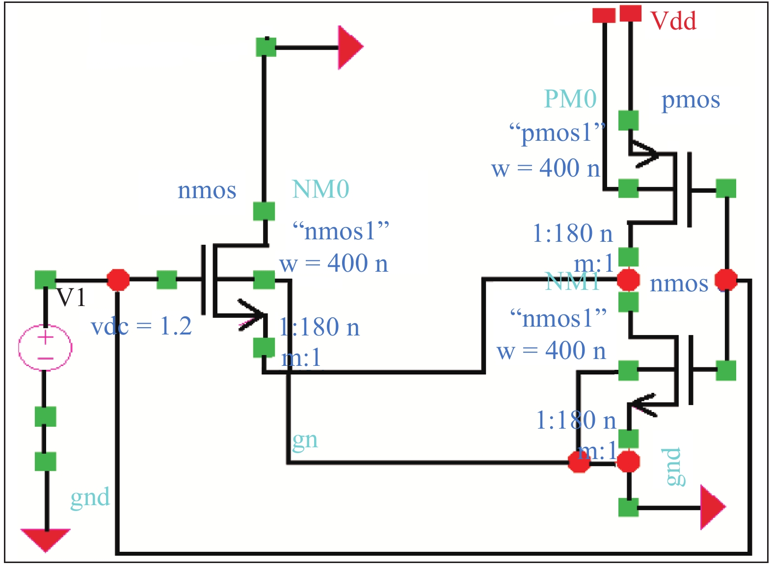
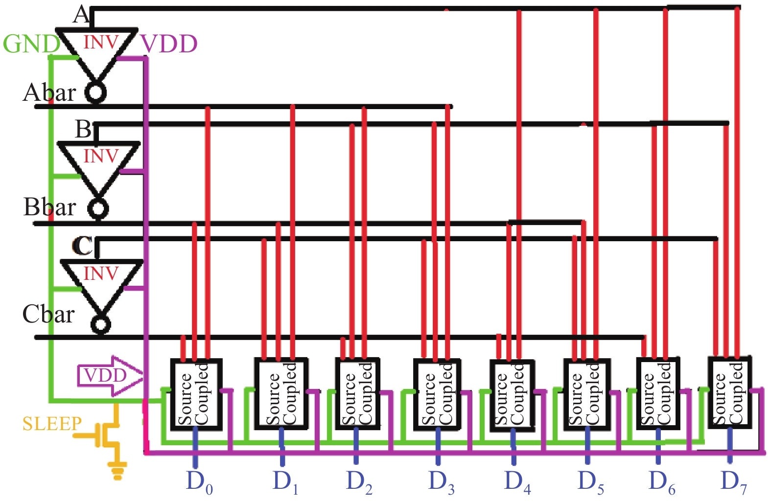
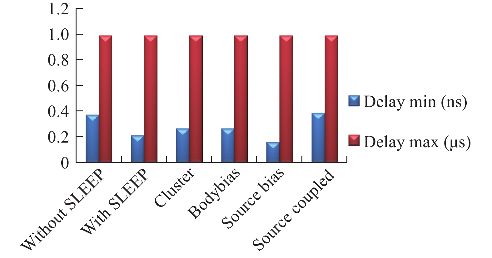
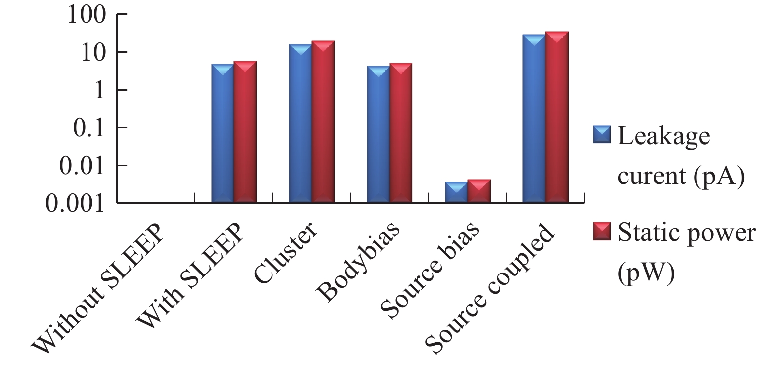
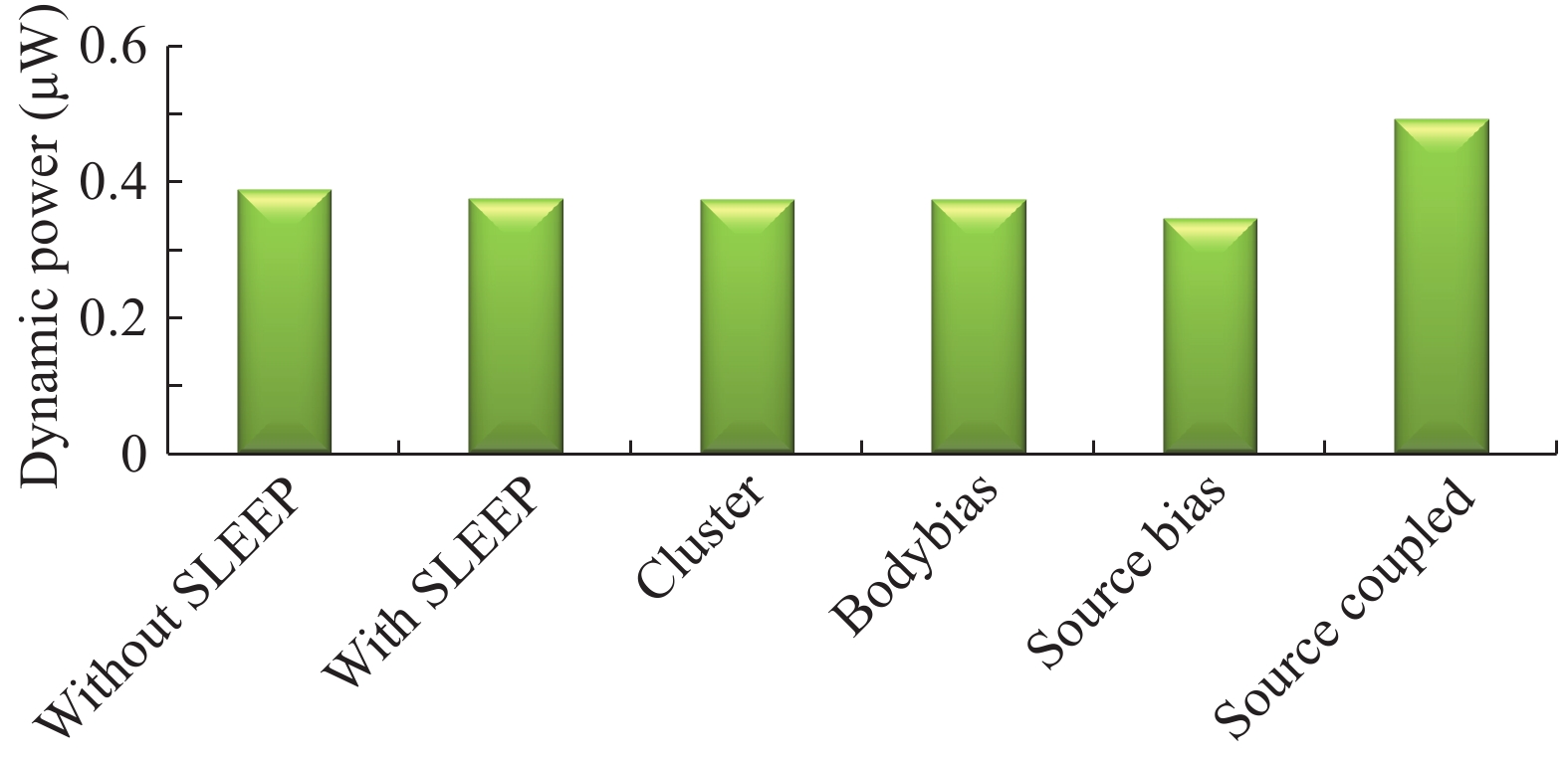
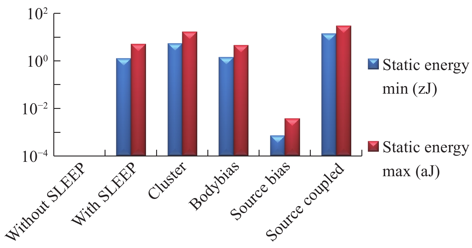
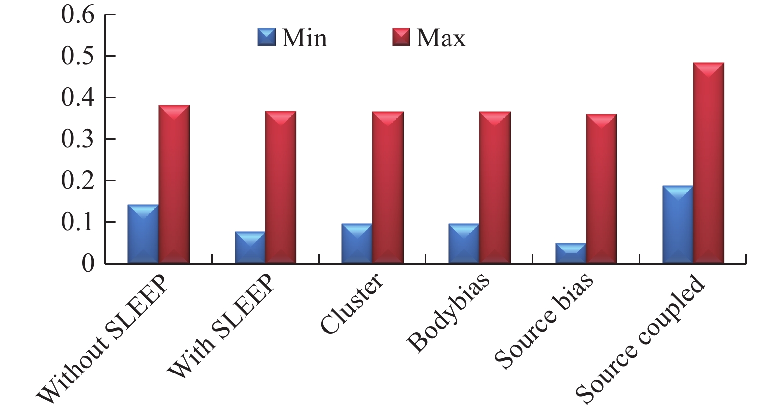
Researchers have proposed many circuit techniques to reduce leakage power dissipation in memory cells. If we want to reduce the overall power in the memory system, we have to work on the input circuitry of memory architecture i.e. row and column decoder. In this research work, low leakage power with a high speed row and column decoder for memory array application is designed and four new techniques are proposed. In this work, the comparison of cluster DECODER, body bias DECODER, source bias DECODER, and source coupling DECODER are designed and analyzed for memory array application. Simulation is performed for the comparative analysis of different DECODER design parameters at 180 nm GPDK technology file using the CADENCE tool. Simulation results show that the proposed source bias DECODER circuit technique decreases the leakage current by 99.92% and static energy by 99.92% at a supply voltage of 1.2 V. The proposed circuit also improves dynamic power dissipation by 5.69%, dynamic PDP/EDP 65.03% and delay 57.25% at 1.2 V supply voltage.


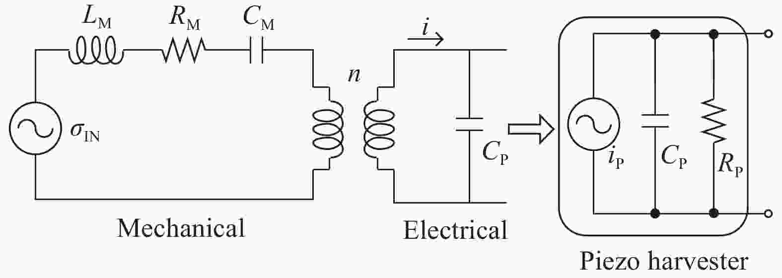
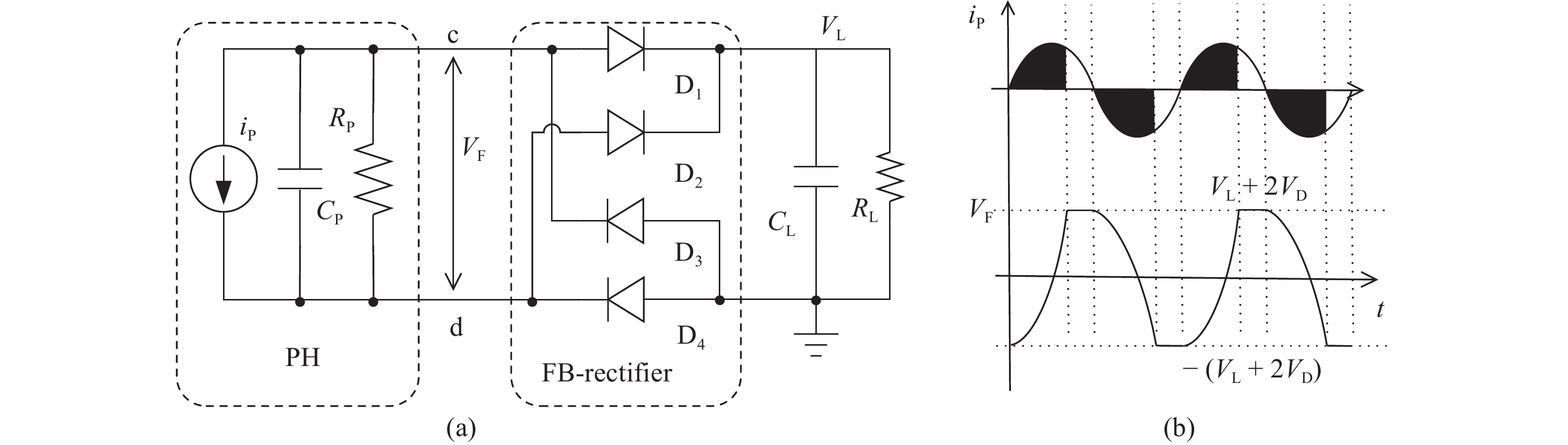
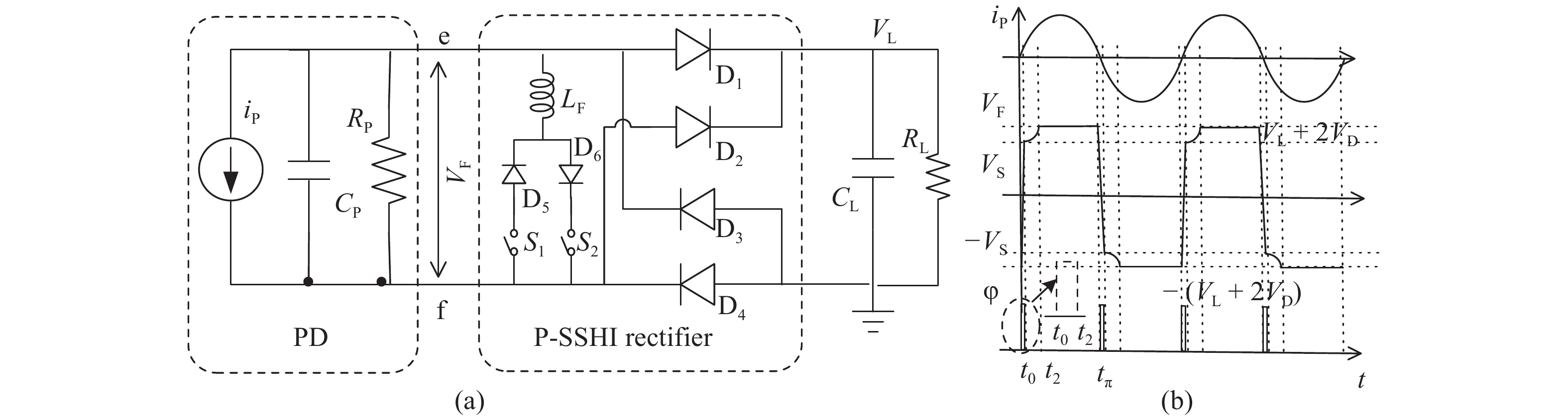
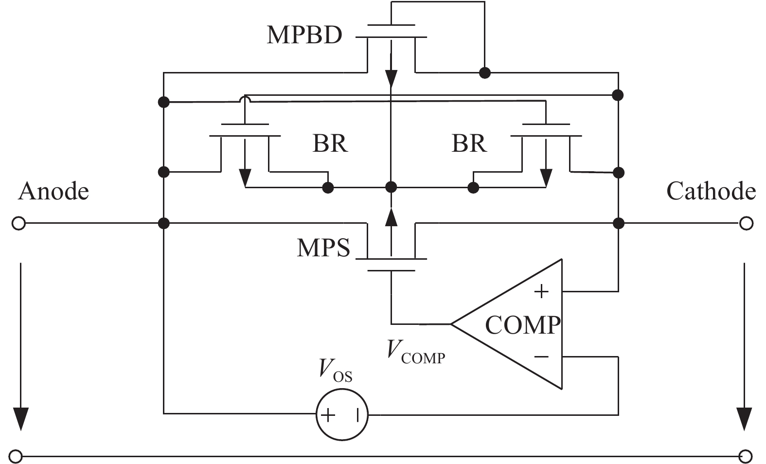
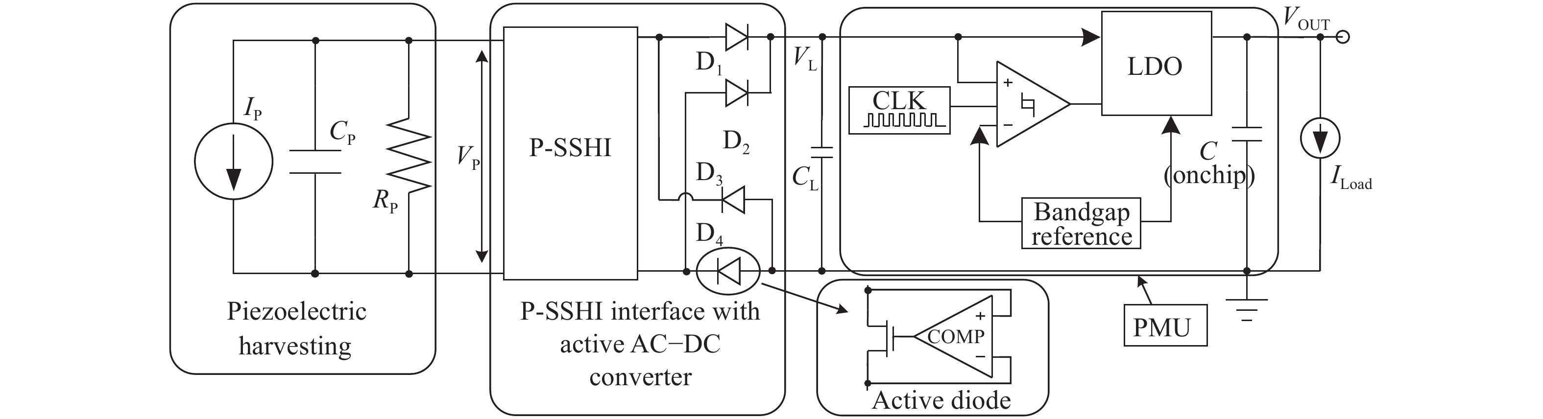
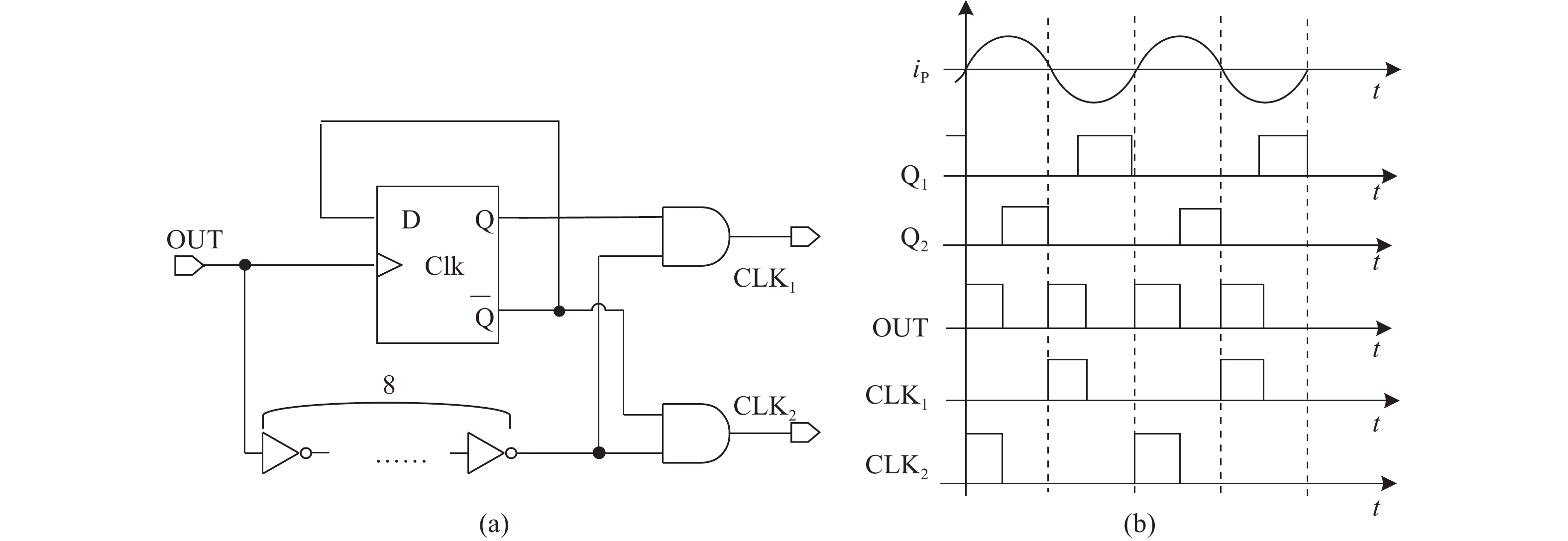
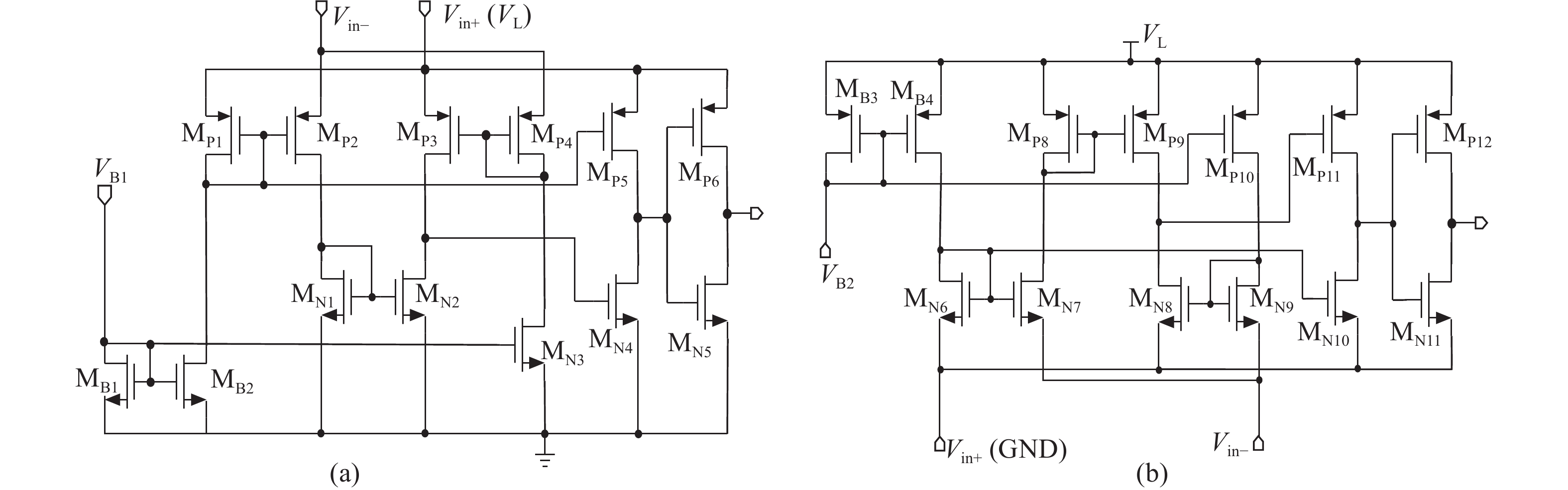
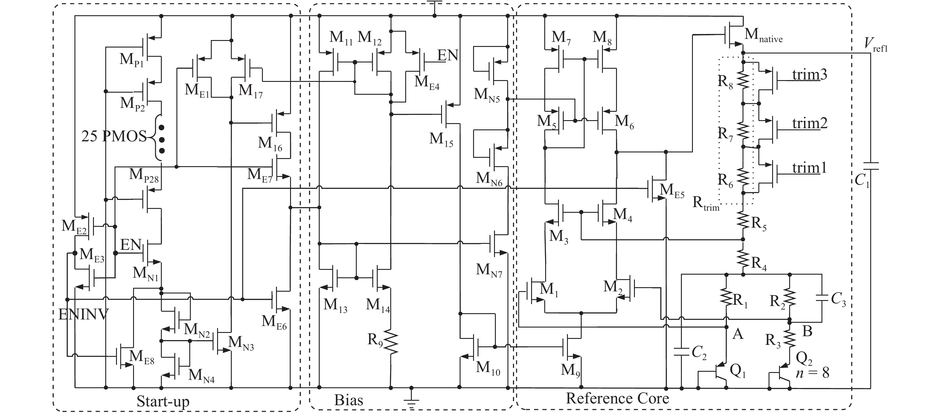
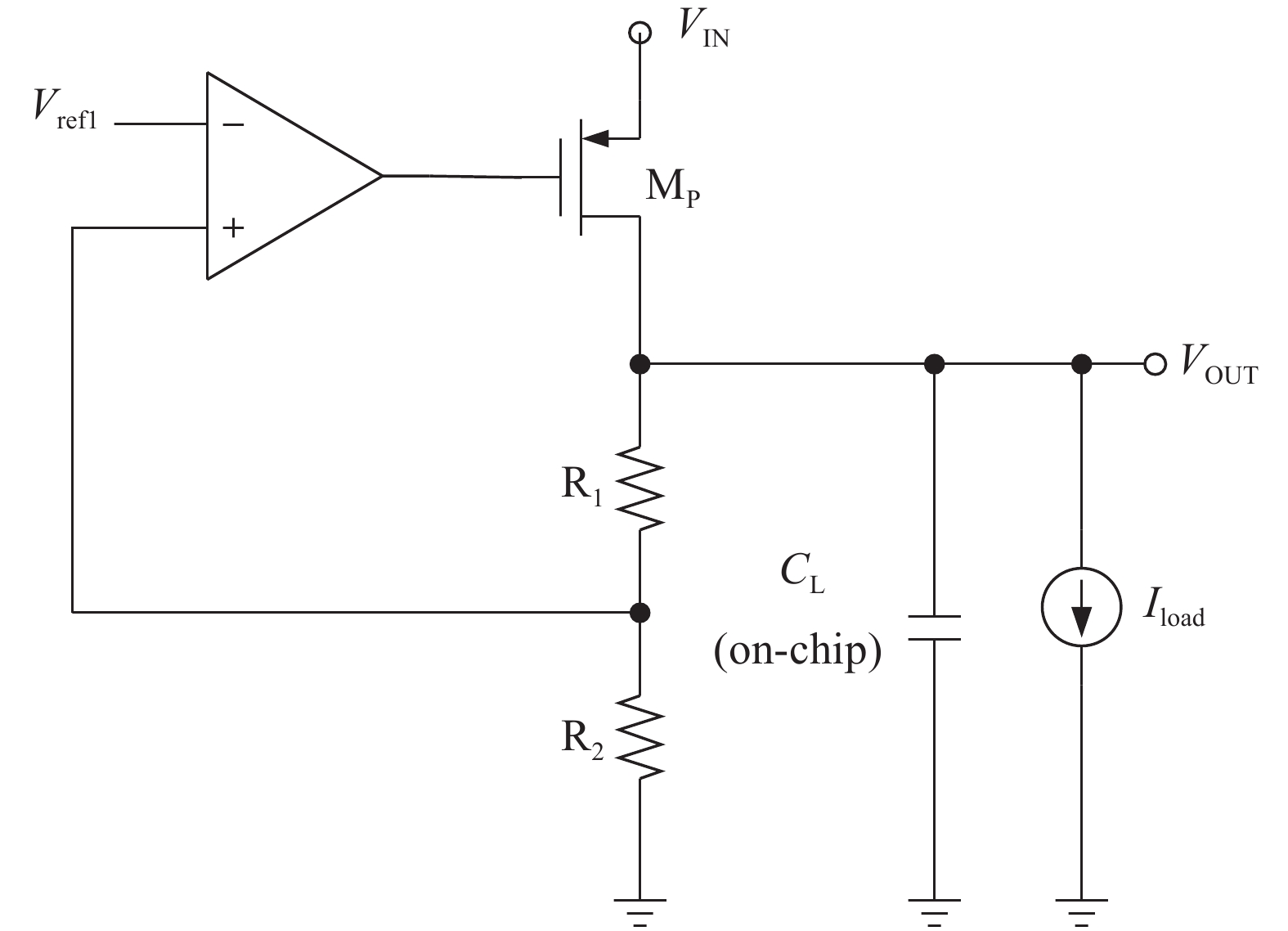
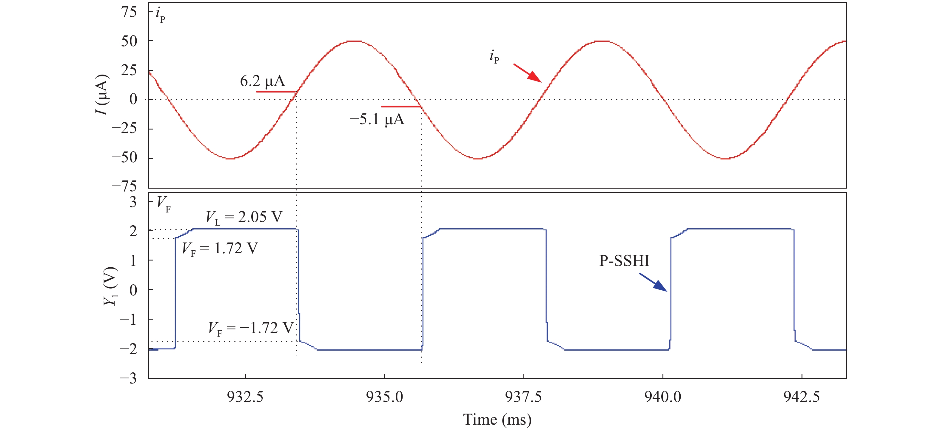
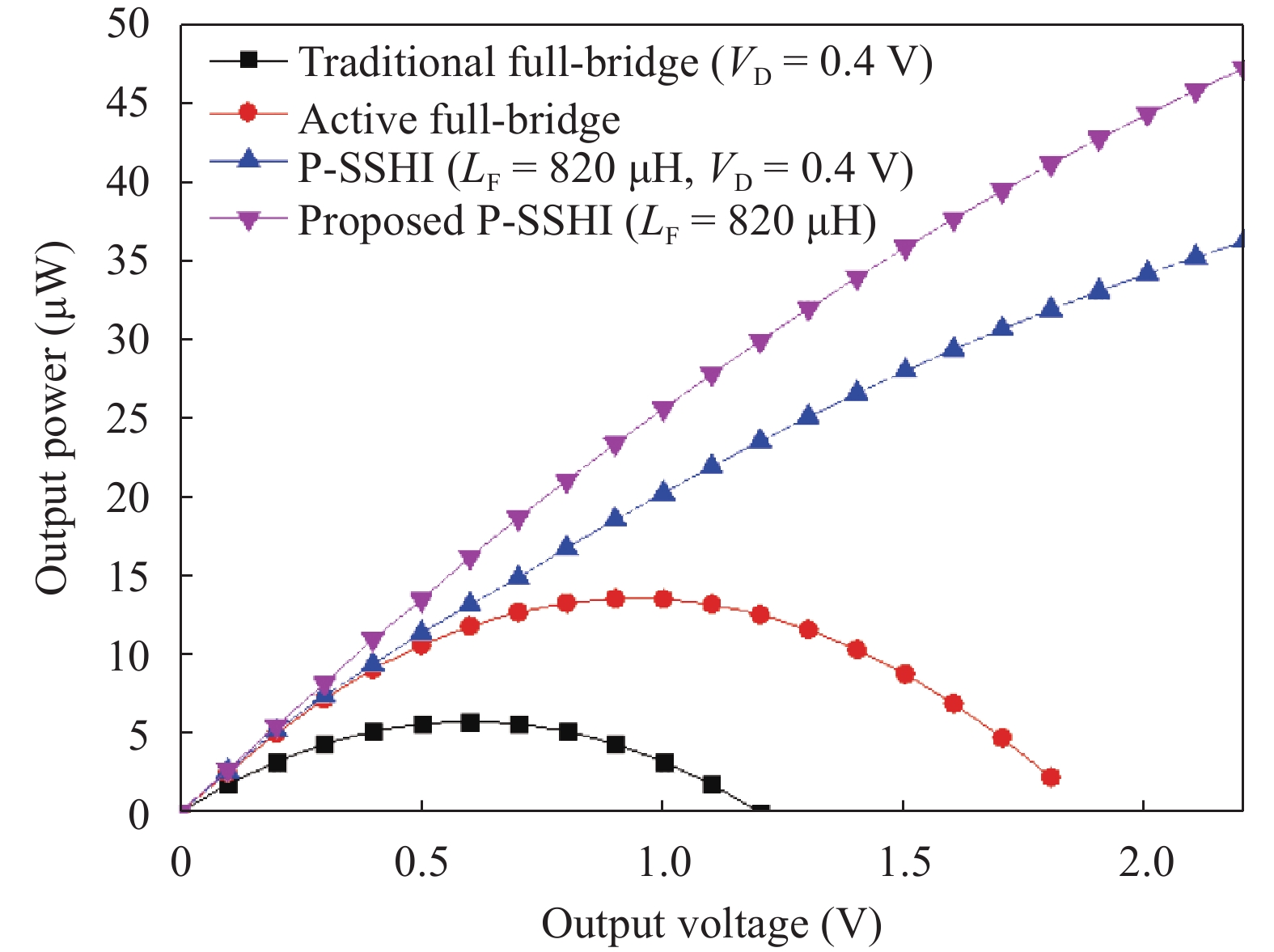
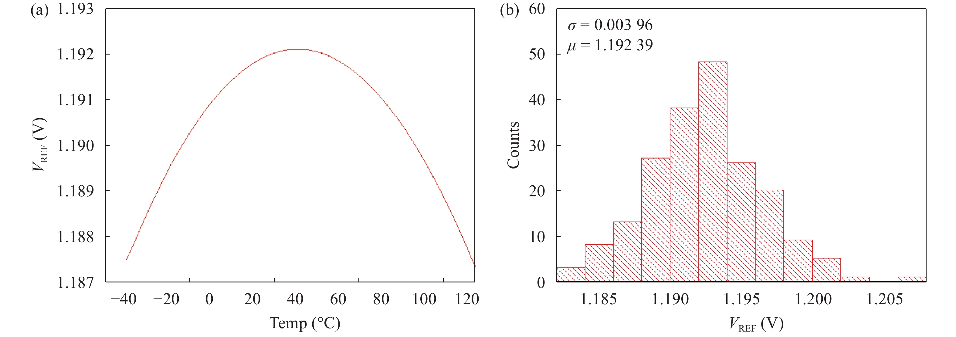
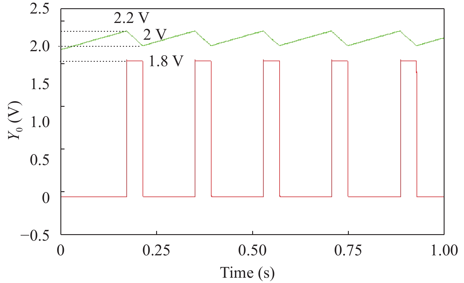
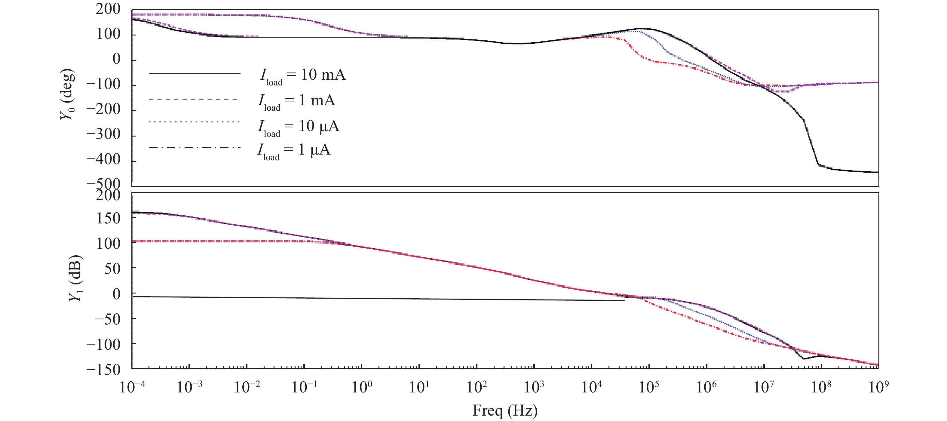
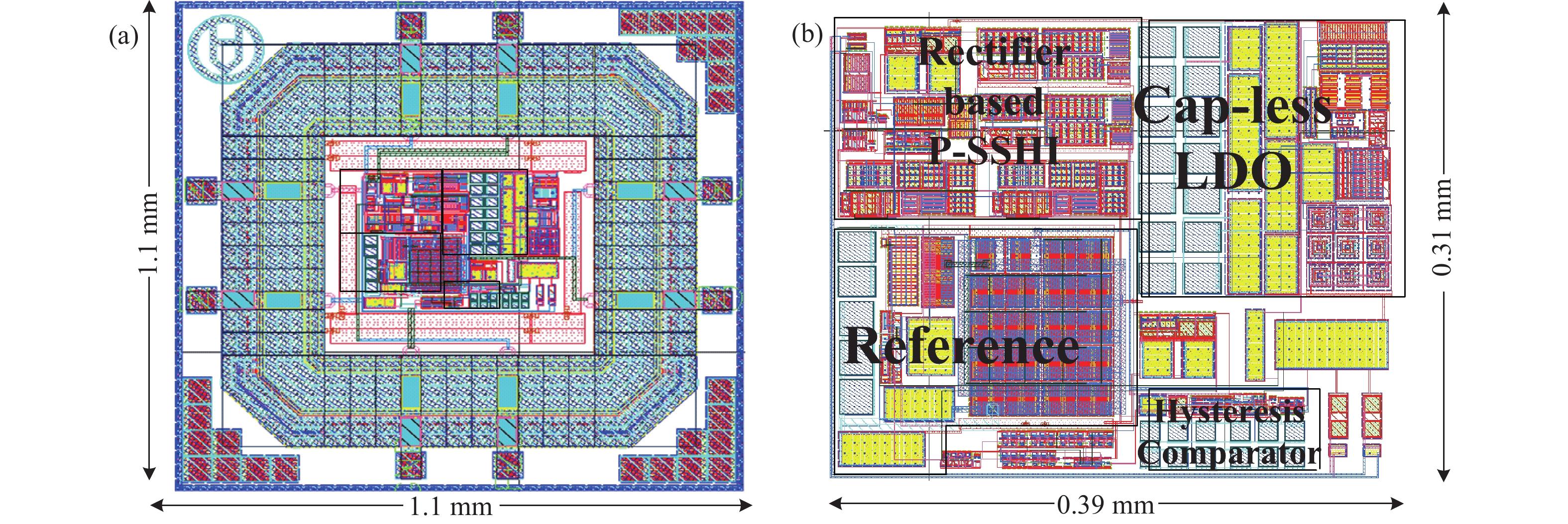
The key to self-powered technique is initiative to harvest energy from the surrounding environment. Harvesting energy from an ambient vibration source utilizing piezoelectrics emerged as a popular method. Efficient interface circuits become the main limitations of existing energy harvesting techniques. In this paper, an interface circuit for piezoelectric energy harvesting is presented. An active full bridge rectifier is adopted to improve the power efficiency by reducing the conduction loss on the rectifying path. A parallel synchronized switch harvesting on inductor (P-SSHI) technique is used to improve the power extraction capability from piezoelectric harvester, thereby trying to reach the theoretical maximum output power. An intermittent power management unit (IPMU) and an output capacitor-less low drop regulator (LDO) are also introduced. Active diodes (AD) instead of traditional passive ones are used to reduce the voltage loss over the rectifier, which results in a good power efficiency. The IPMU with hysteresis comparator ensures the interface circuit has a large transient output power by limiting the output voltage ranges from 2.2 to 2 V. The design is fabricated in a SMIC 0.18 μm CMOS technology. Simulation results show that the flipping efficiency of the P-SSHI circuit is over 80% with an off-chip inductor value of 820 μH. The output power the proposed rectifier can obtain is 44.4 μW, which is 6.7× improvement compared to the maximum output power of a traditional rectifier. Both the active diodes and the P-SSHI help to improve the output power of the proposed rectifier. LDO outputs a voltage of 1.8 V with the maximum 90% power efficiency. The proposed P-SSHI rectifier interface circuit can be self-powered without the need for additional power supply.


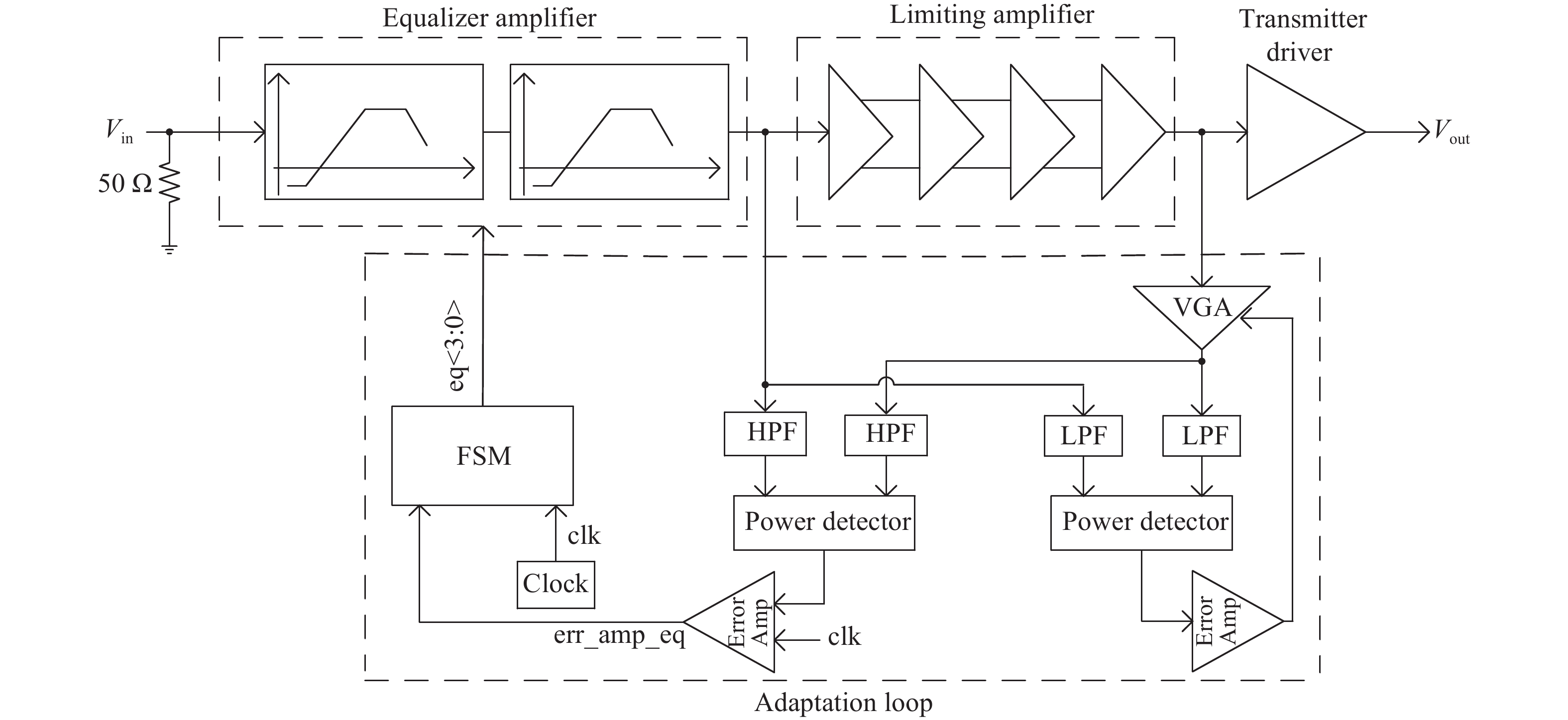
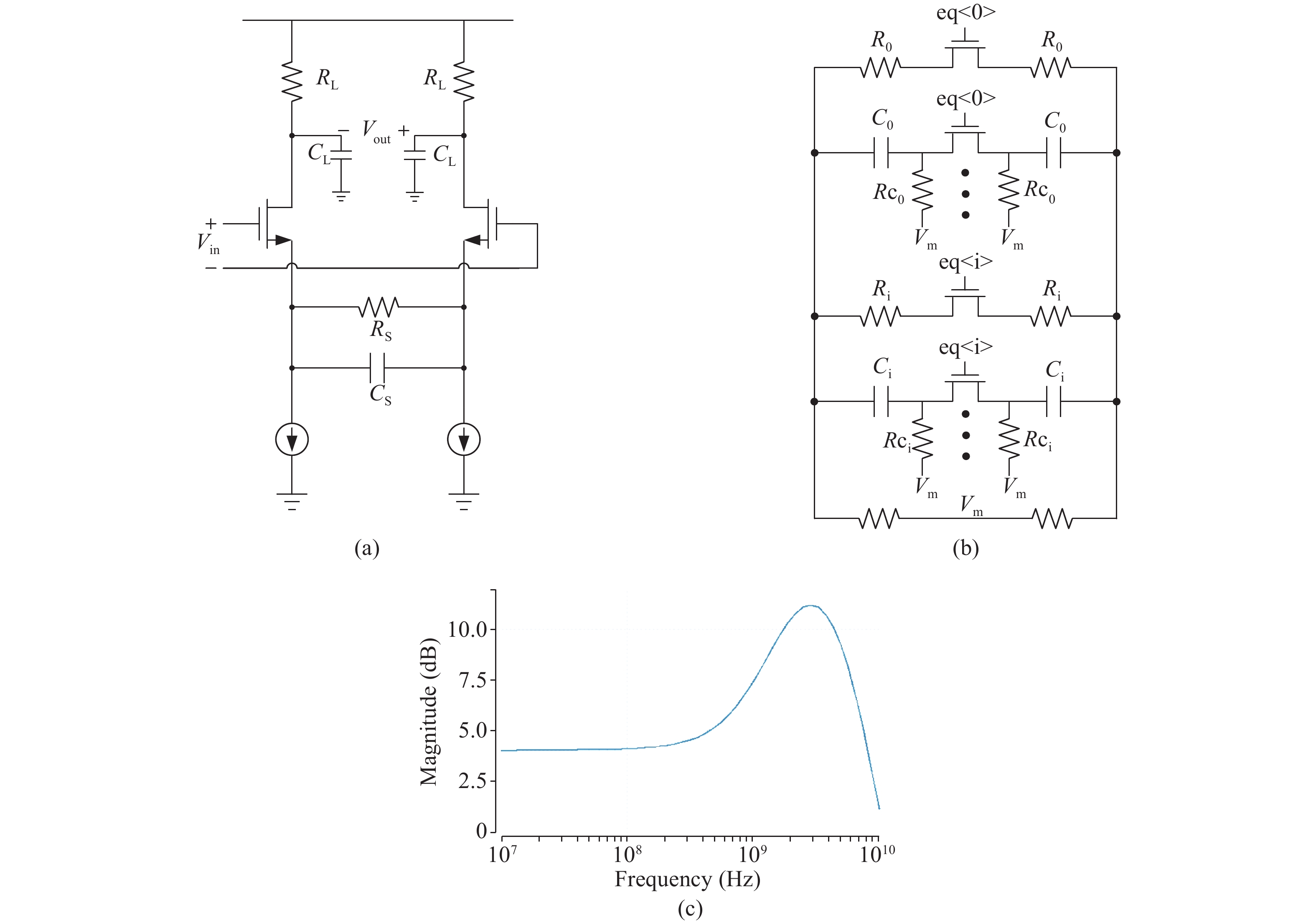
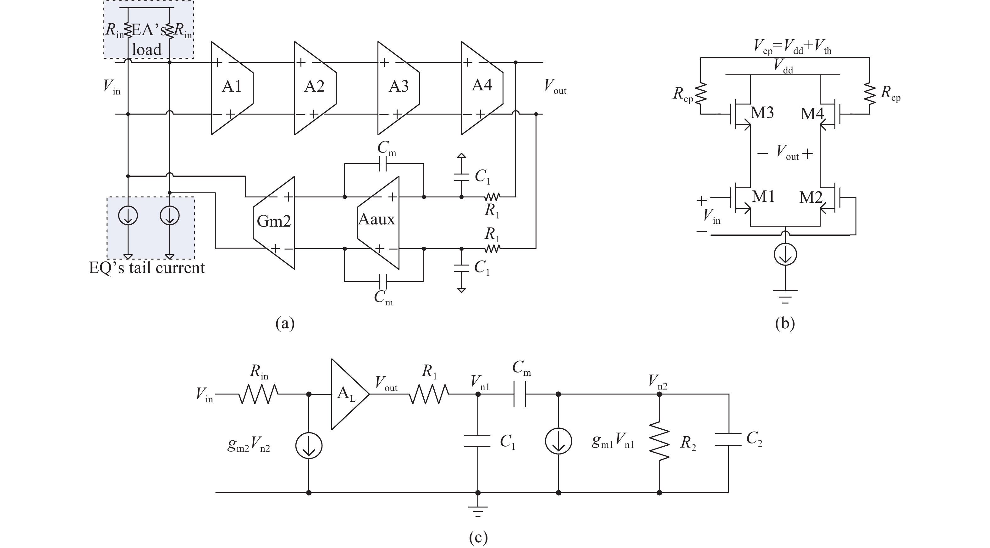
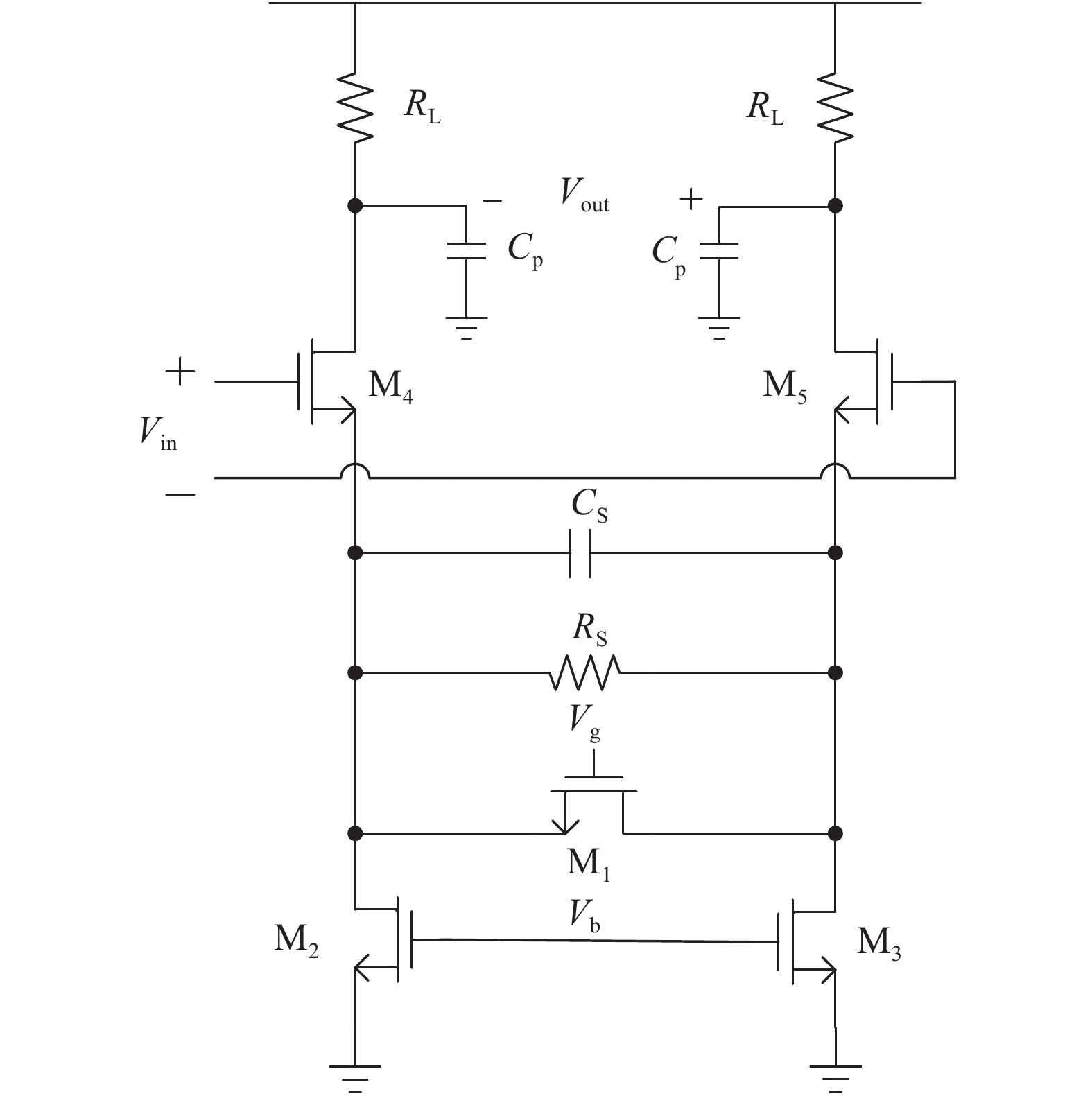
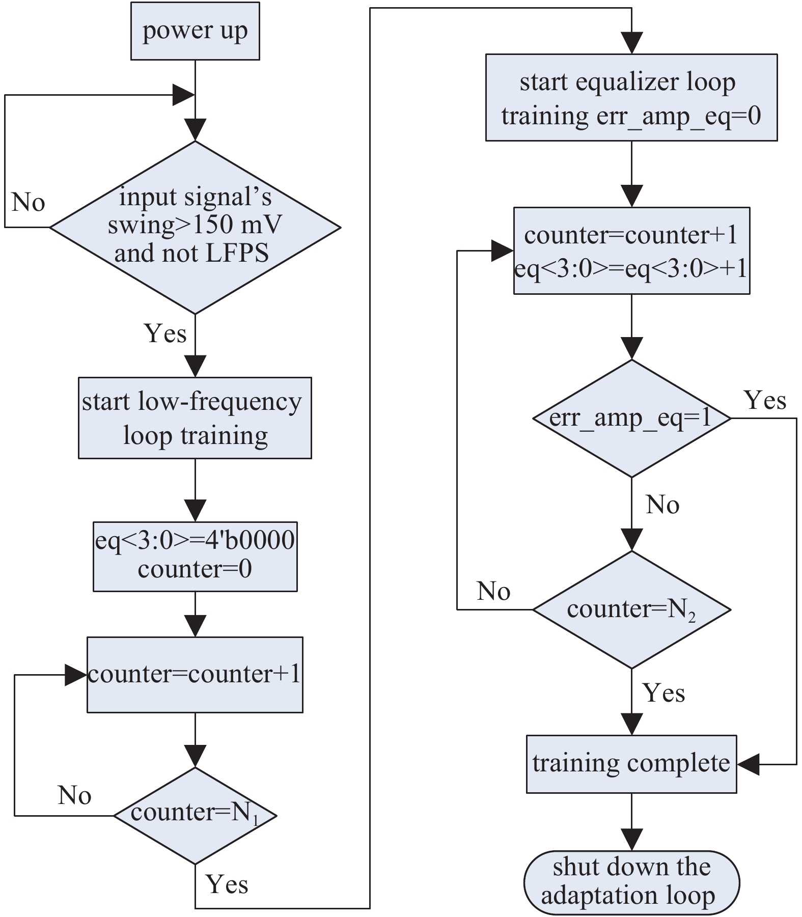
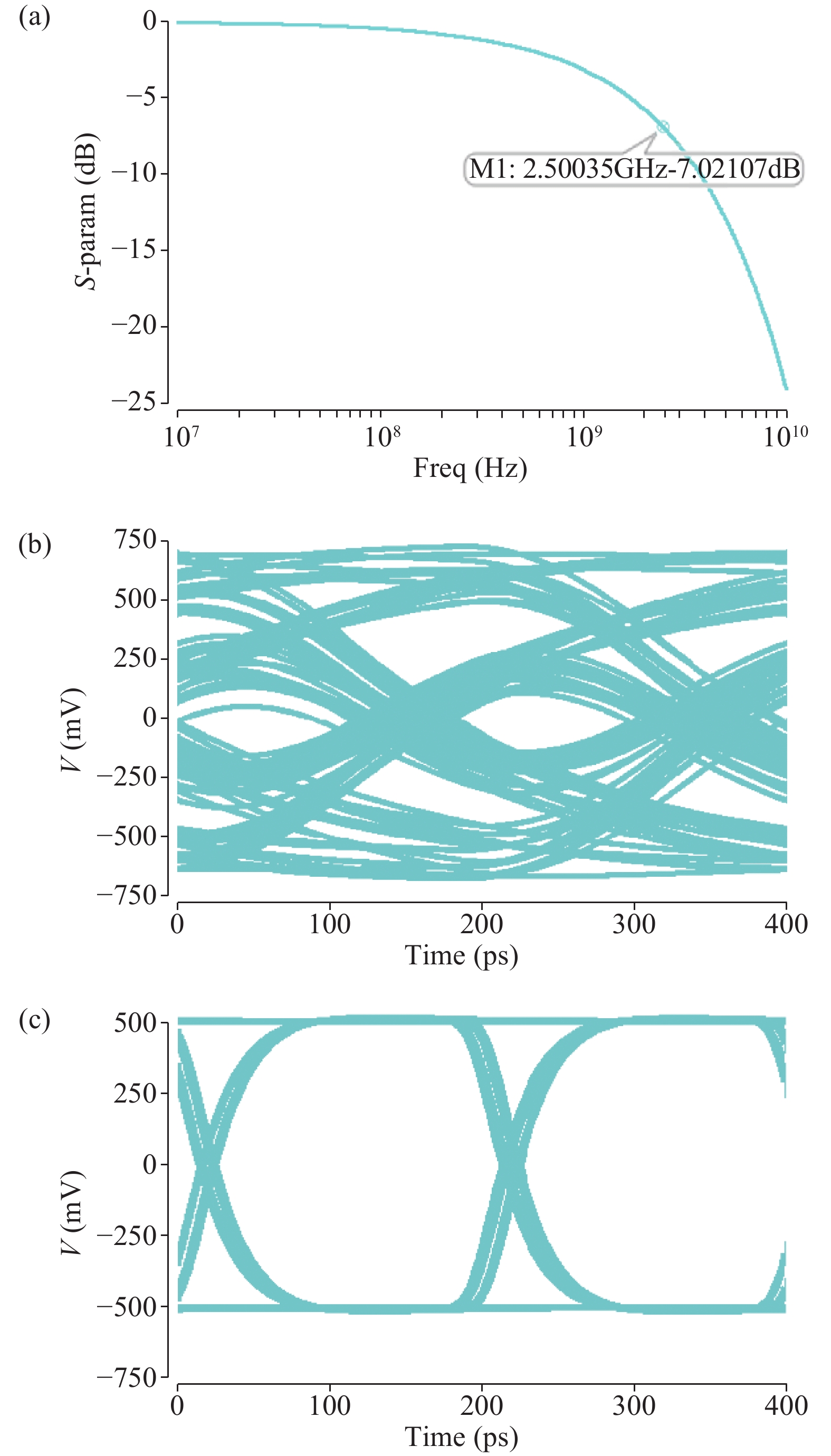
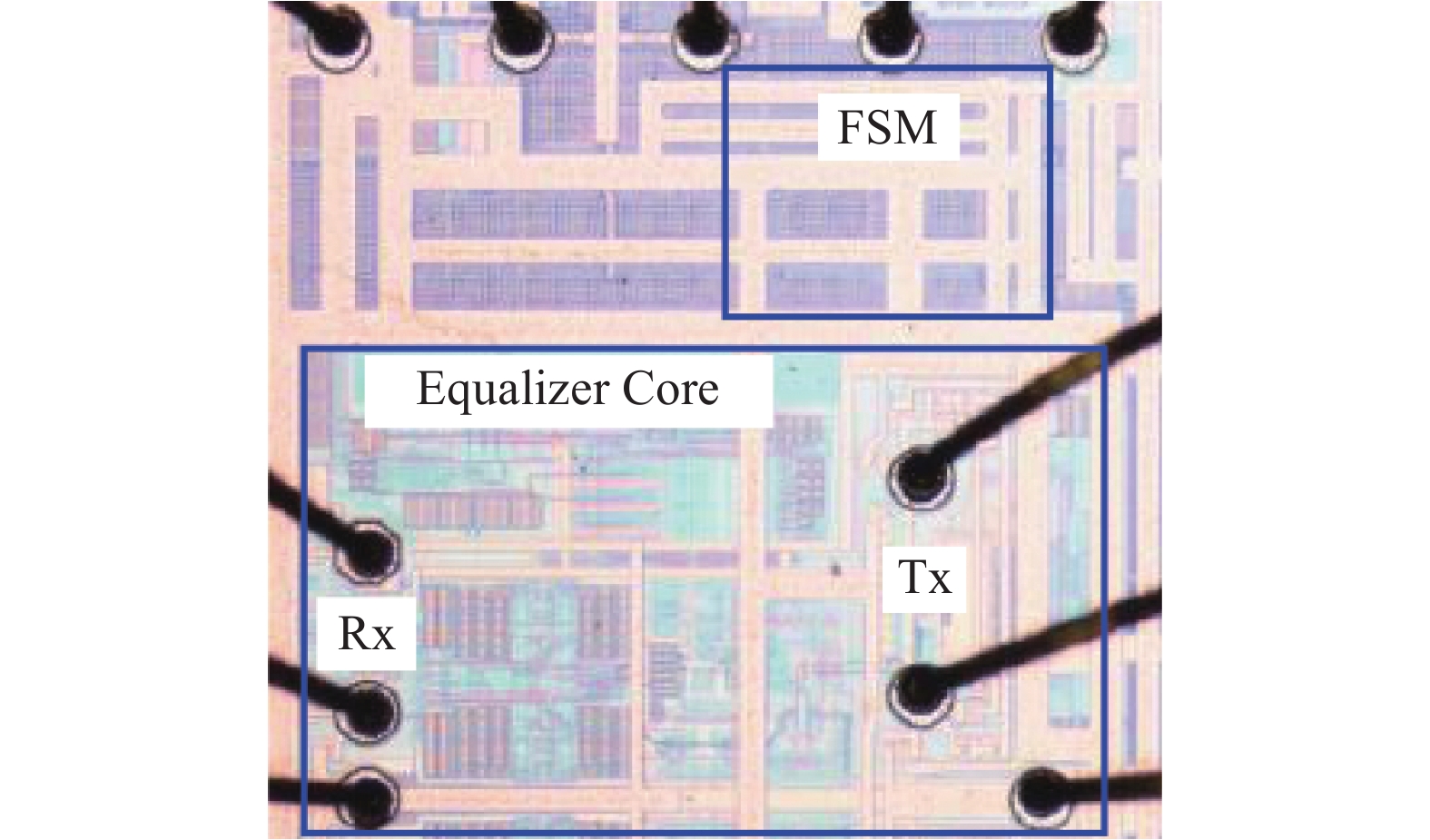
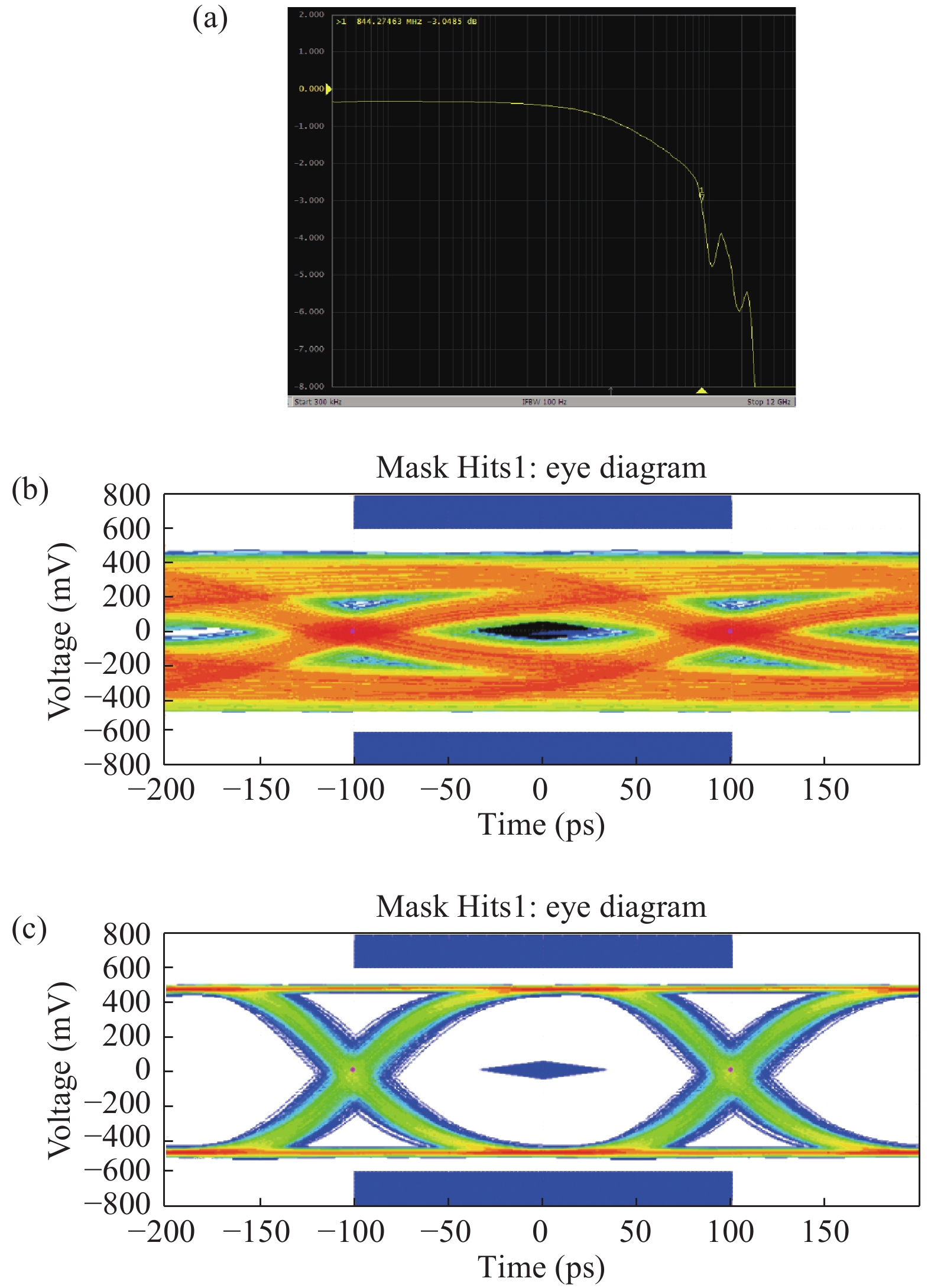
A 5 Gb/s adaptive equalizer with a new adaptation scheme is presented here by using 0.13 μm CMOS process. The circuit consists of the combination of equalizer amplifier, limiter amplifier and adaptation loop. The adaptive algorithm exploits both the low frequency gain loop and the equalizer loop to minimize the inter-symbol interference (ISI) for a variety of cable characteristics. In addition, an offset cancellation loop is used to alleviate the offset influence of the signal path. The adaptive equalizer core occupies an area of 0.3567 mm2 and consumes a power consumption of 81.7 mW with 1.8 V power supply. Experiment results demonstrate that the equalizer could compensate for a designed cable loss with 0.23 UI peak-to-peak jitter.
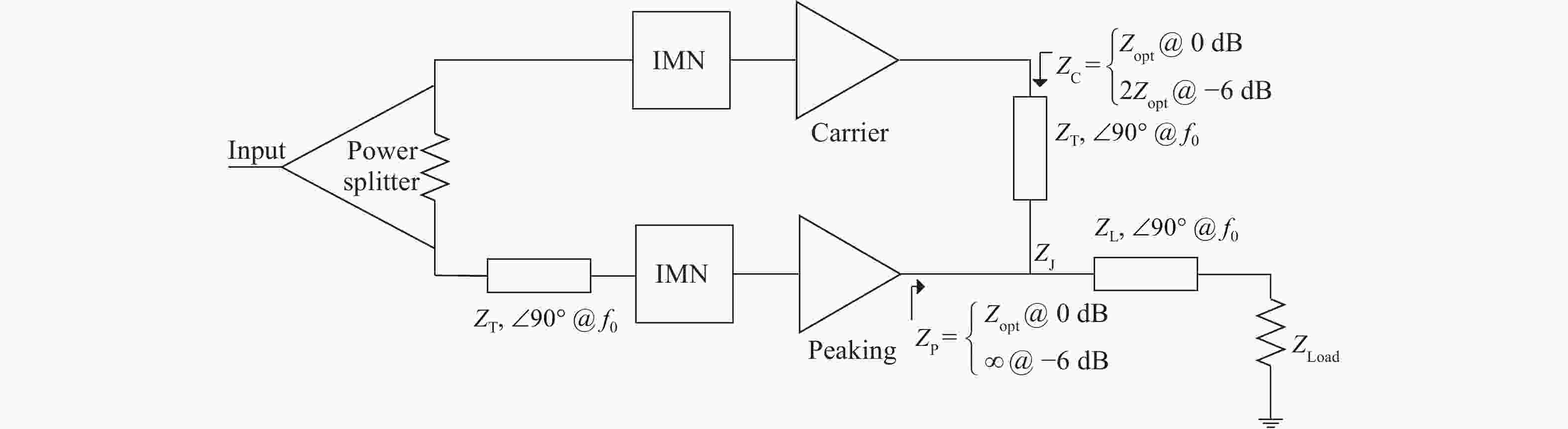
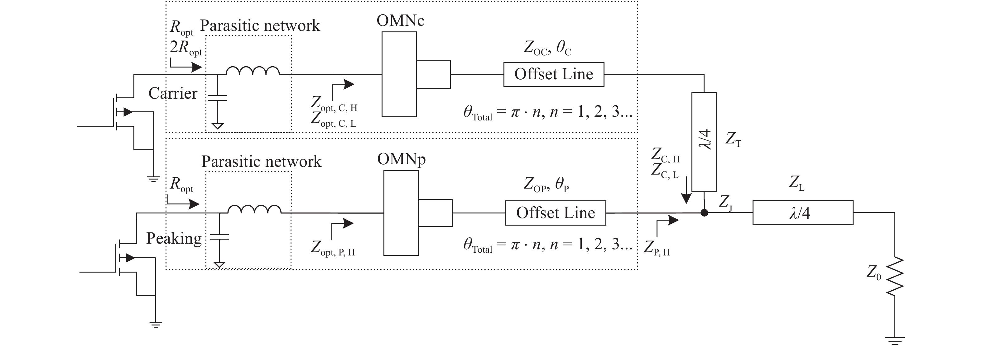
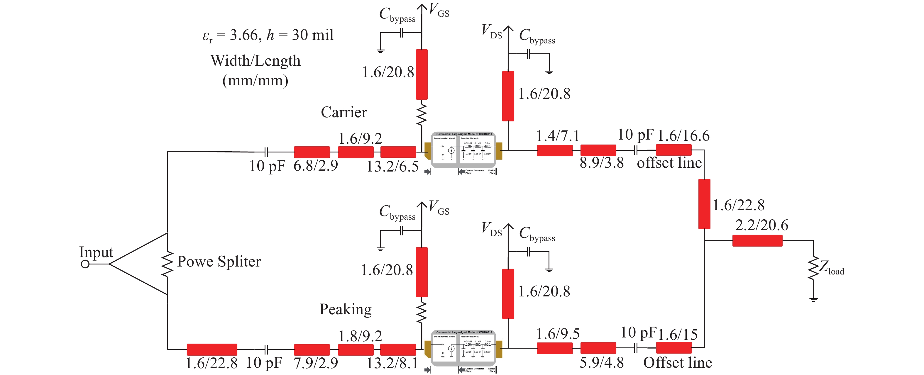
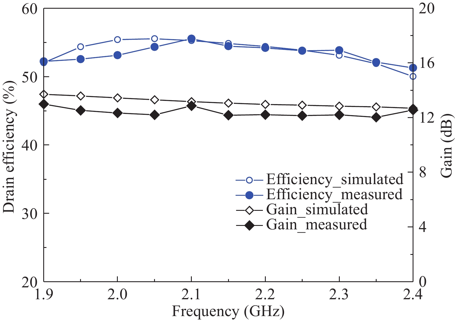
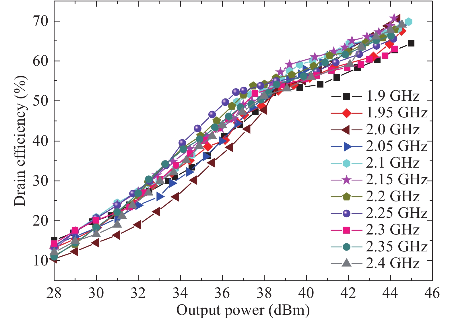
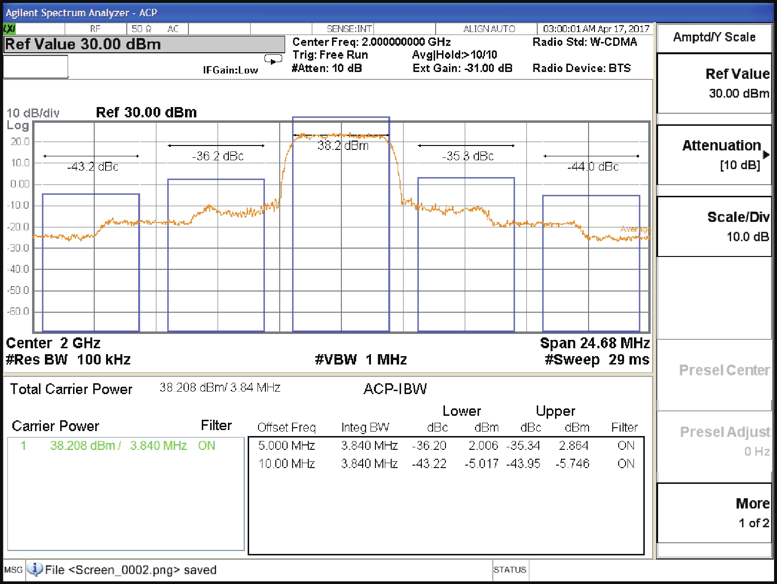
This paper proposes a method for broadband and high-efficiency amplification of Doherty power amplifier (DPA) using symmetric devices. In order to achieve the perfect load modulation, the carrier amplifier output circuit total power length is designed to odd multiple of 90°, and the peak amplifier output total power length is designed to even multiple of 180°. The proposed method is demonstrated by designing a broadband high-efficiency DPA using identical 10-W packaged GaN HEMT devices. Measurement results show that over 51% drain efficiency is achieved at 6-dB back-off power, over the frequency band of 1.9–2.4 GHz.


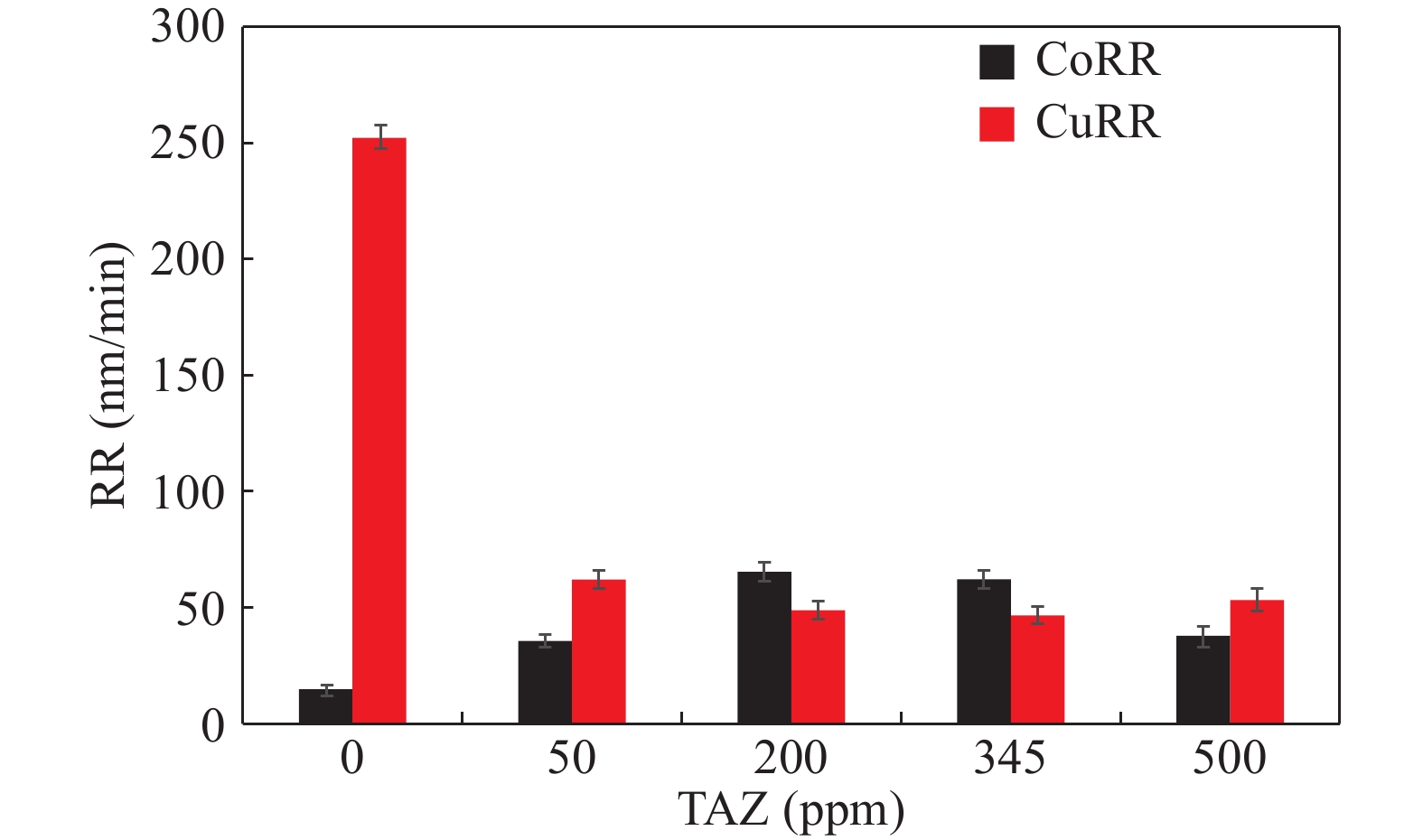
Cobalt has become a new type of barrier material with its unique advantages since the copper-interconnects in the great-large scale integrated circuits (GLSI) into 10 nm and below technical nodes, but cobalt and copper have severe galvanic corrosion during chemical–mechanical flattening. The effect of 1,2,4-triazole on Co/Cu galvanic corrosion in alkaline slurry and the control of rate selectivity of copper and cobalt were investigated in this work. The results of electrochemical experiments and polishing experiments had indicated that a certain concentration of 1,2,4-triazole could form a layer of insoluble and dense passive film on the surface of cobalt and copper, which reduced the corrosion potential difference between cobalt and copper. Meantime, the removal rate of cobalt and copper could be effectively controlled according to demand during the CMP process. When the study optimized slurry was composed of 0.5 wt% colloidal silica, 0.1 %vol. hydrogen peroxide, 0.05 wt% FA/O, 345 ppm 1,2,4-triazole, cobalt had higher corrosion potential than copper and the galvanic corrosion could be reduced effectively when the corrosion potential difference between them decreased to 1 mV and the galvanic corrosion current density reached 0.02 nA/cm2. Meanwhile, the removal rate of Co was 62.396 nm/min, the removal rate of Cu was 47.328 nm/min, so that the removal rate ratio of cobalt and copper was 1.32 : 1, which was a good amendment to the dishing pits. The contact potential corrosion of Co/Cu was very weak, which could be better for meeting the requirements of the barrier CMP.