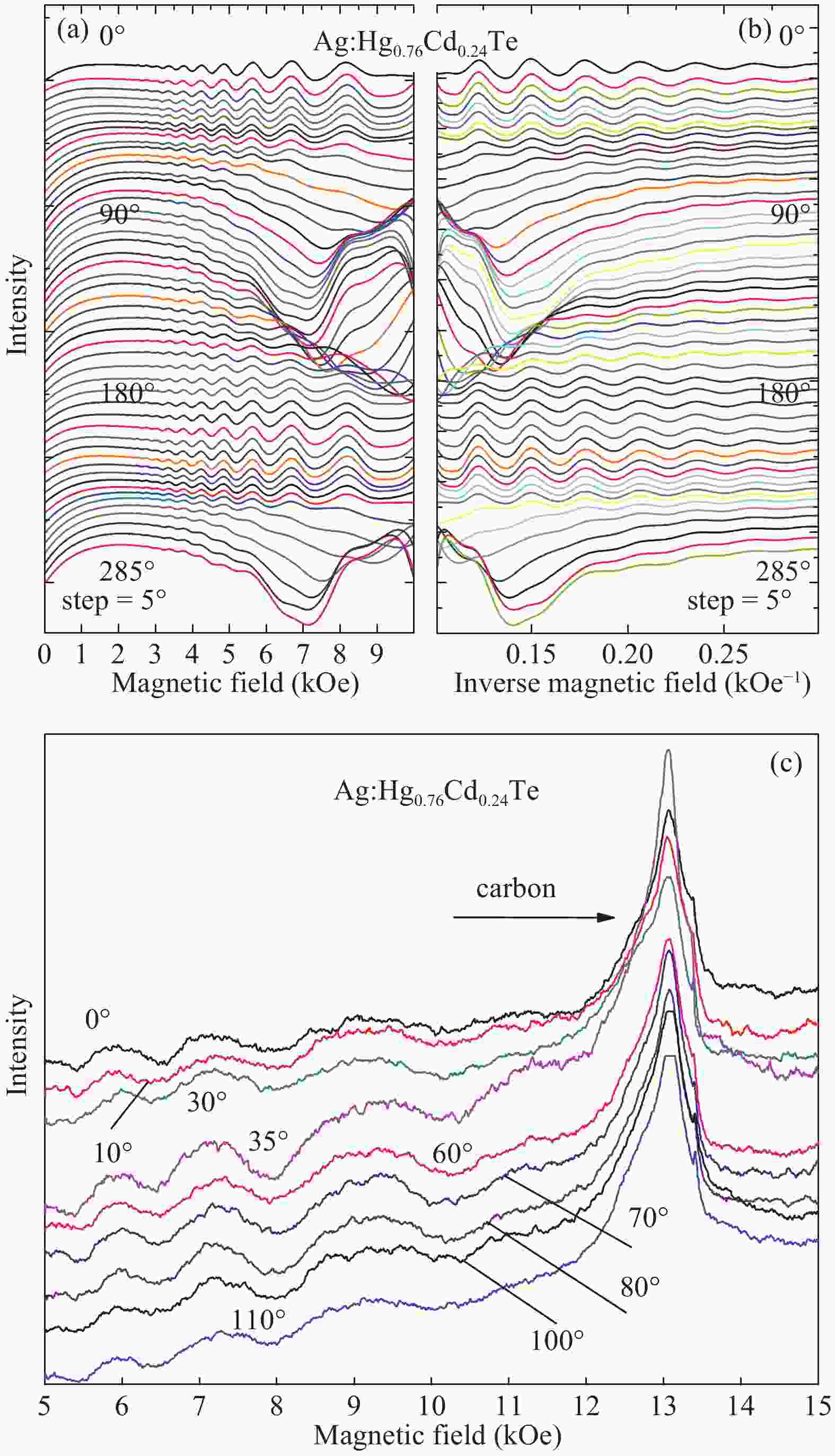
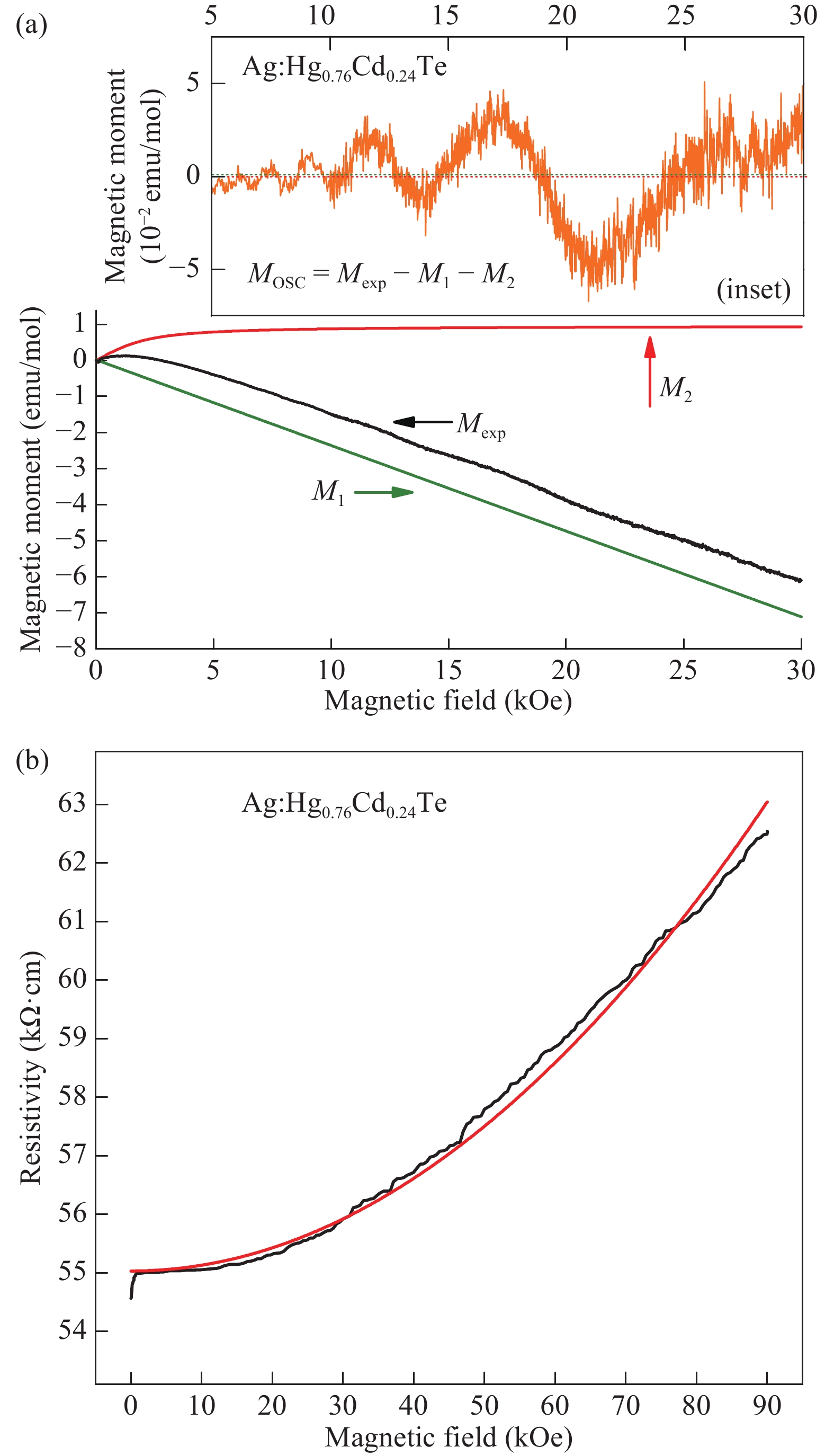
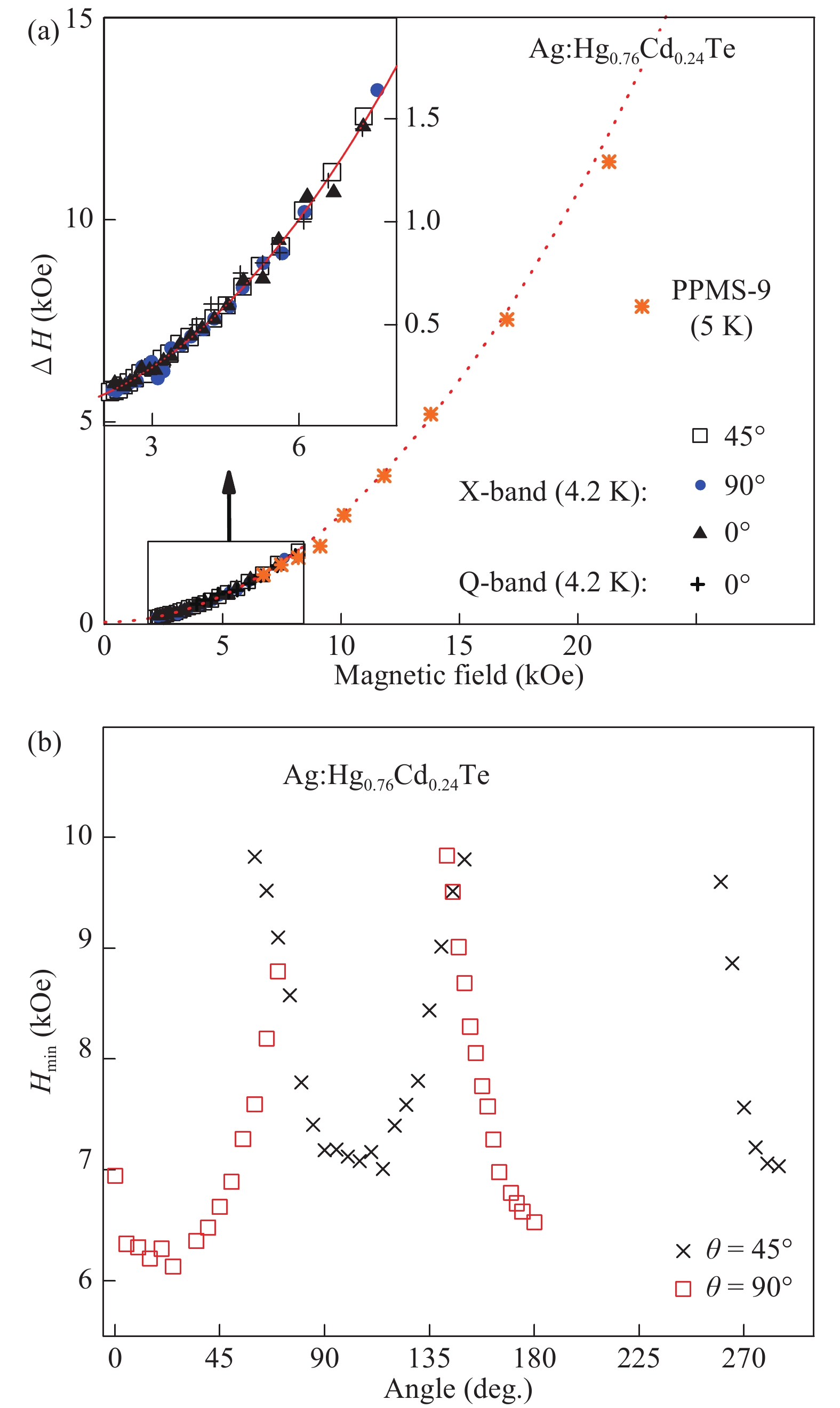
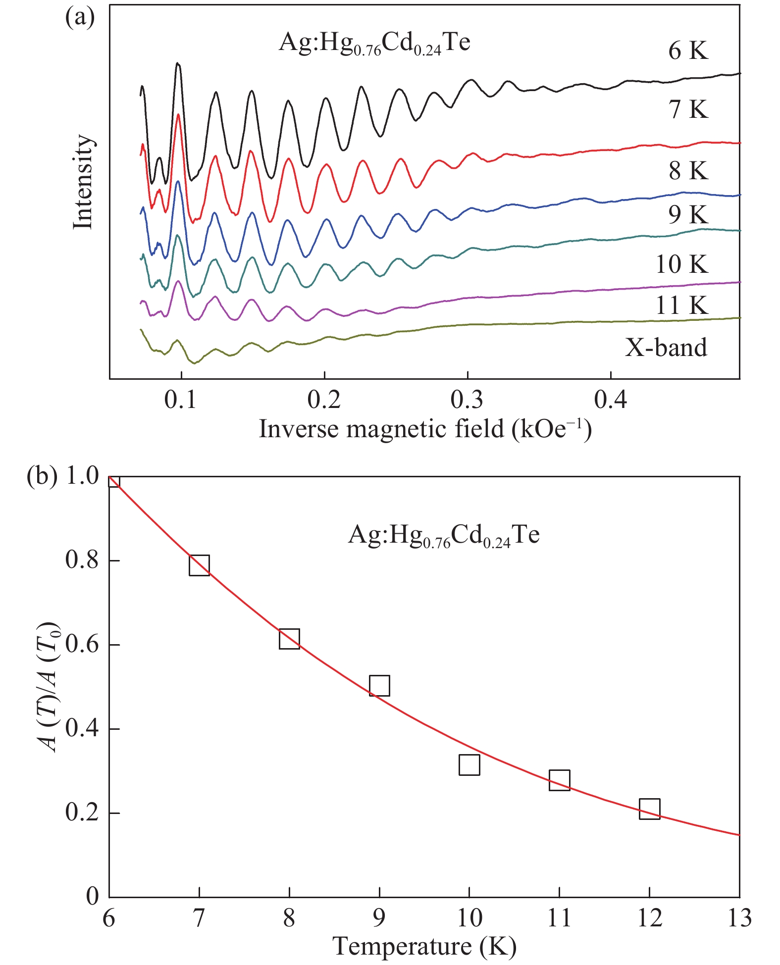
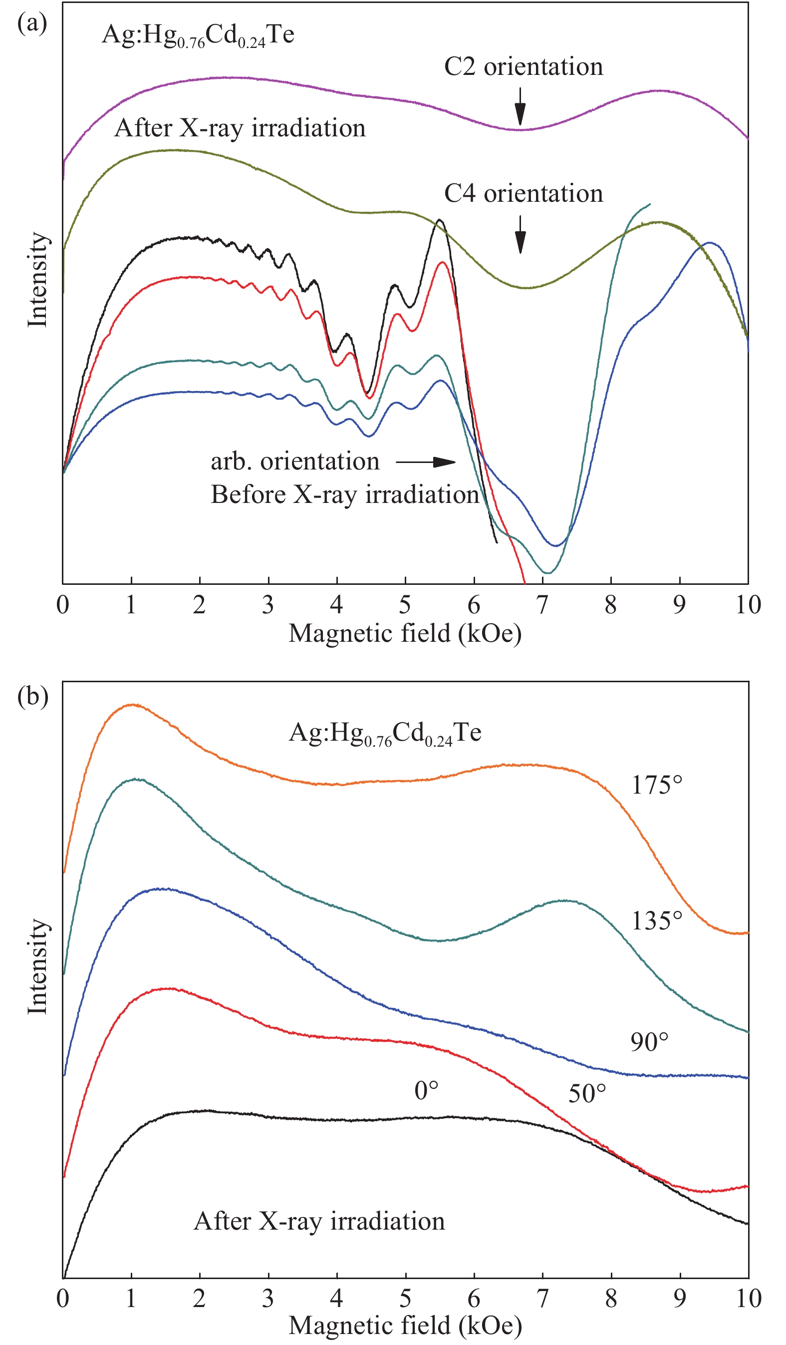
The objects of the investigation were uniformly Ag+ doped Hg0.76Cd0.24Te mercury chalcogenide monocrystals obtained by ion implantation with subsequent thermal annealing over 20 days. After implantation and annealing the conductivity was inverted from n-type with carrier concentration of 1016 cm−3 to p-type with carrier concentration of ≈ 3.9 × 1015 cm−3. The investigations of microwave absorption derivative (dP/dH) showed the existence of strong oscillations in the magnetic field for Ag:Hg0.76Cd0.24Te in the temperature range 4.2–12 K. The concentration and effective mass of charge carrier were determined from oscillation period and temperature dependency of oscillation amplitude. We suppose that this phenomenon is similar to the de Haas–van Alphen effect in weakly correlated electron system with imperfect nesting vector.

We introduce a model of redistribution of point radiation defects, their interaction between themselves and redistribution of their simplest complexes (divacancies and diinterstitials) in a multilayer structure. The model gives a possibility to describe qualitatively nonmonotonicity of distributions of concentrations of radiation defects on interfaces between layers of the multilayer structure. The nonmonotonicity was recently found experimentally. To take into account the nonmonotonicity we modify recently used in literature model for analysis of distribution of concentration of radiation defects. To analyze the model we used an approach of solution of boundary problems, which could be used without crosslinking of solutions on interfaces between layers of the considered multilayer structures.
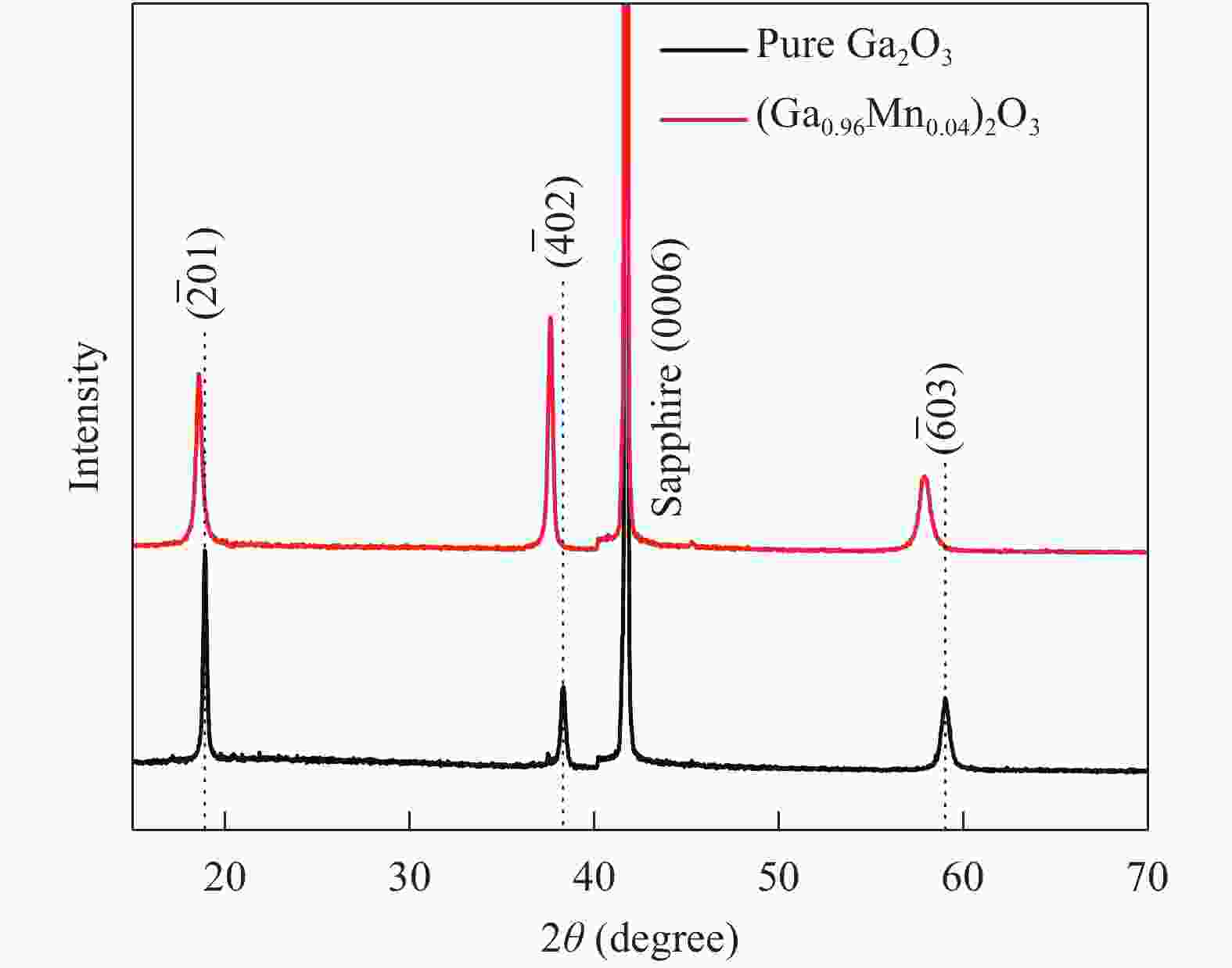
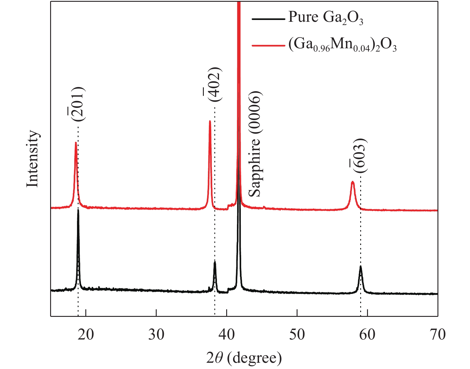
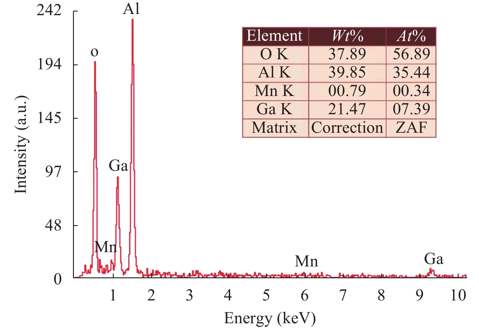
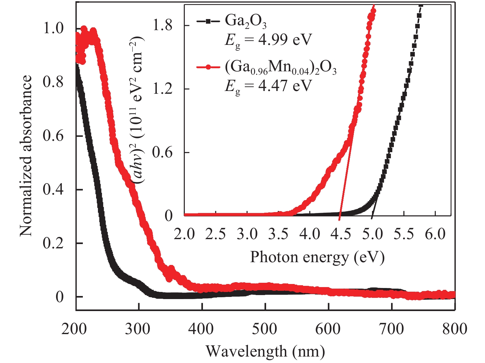
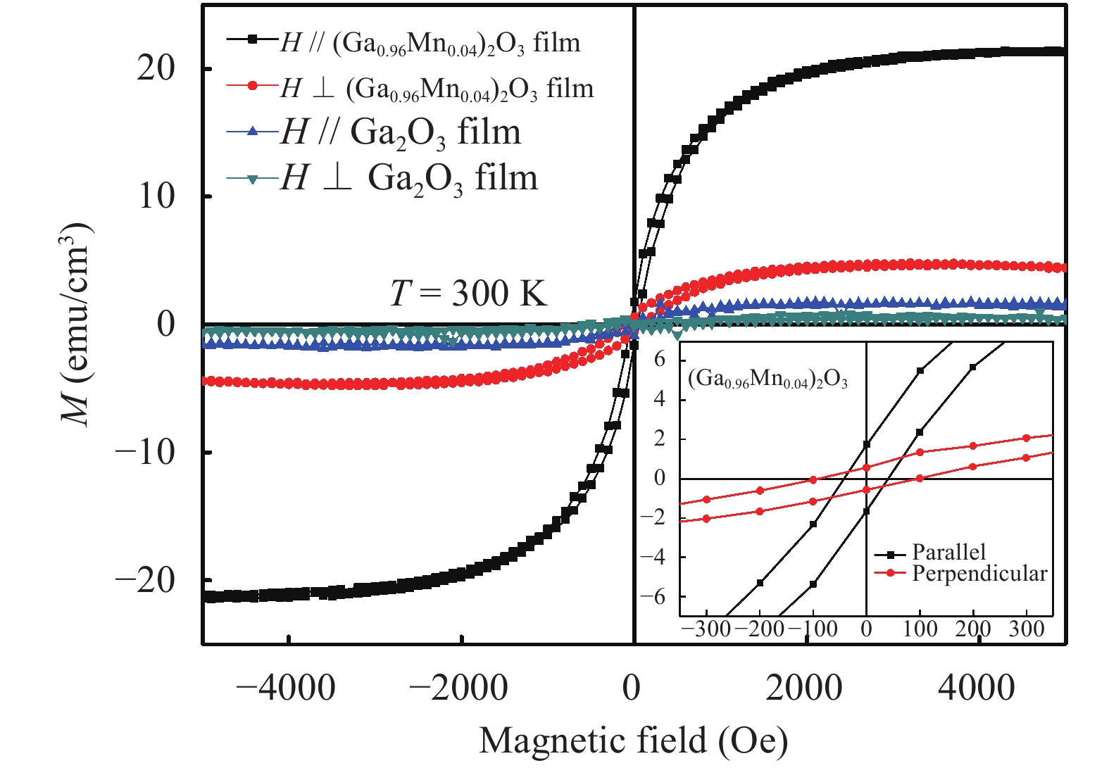
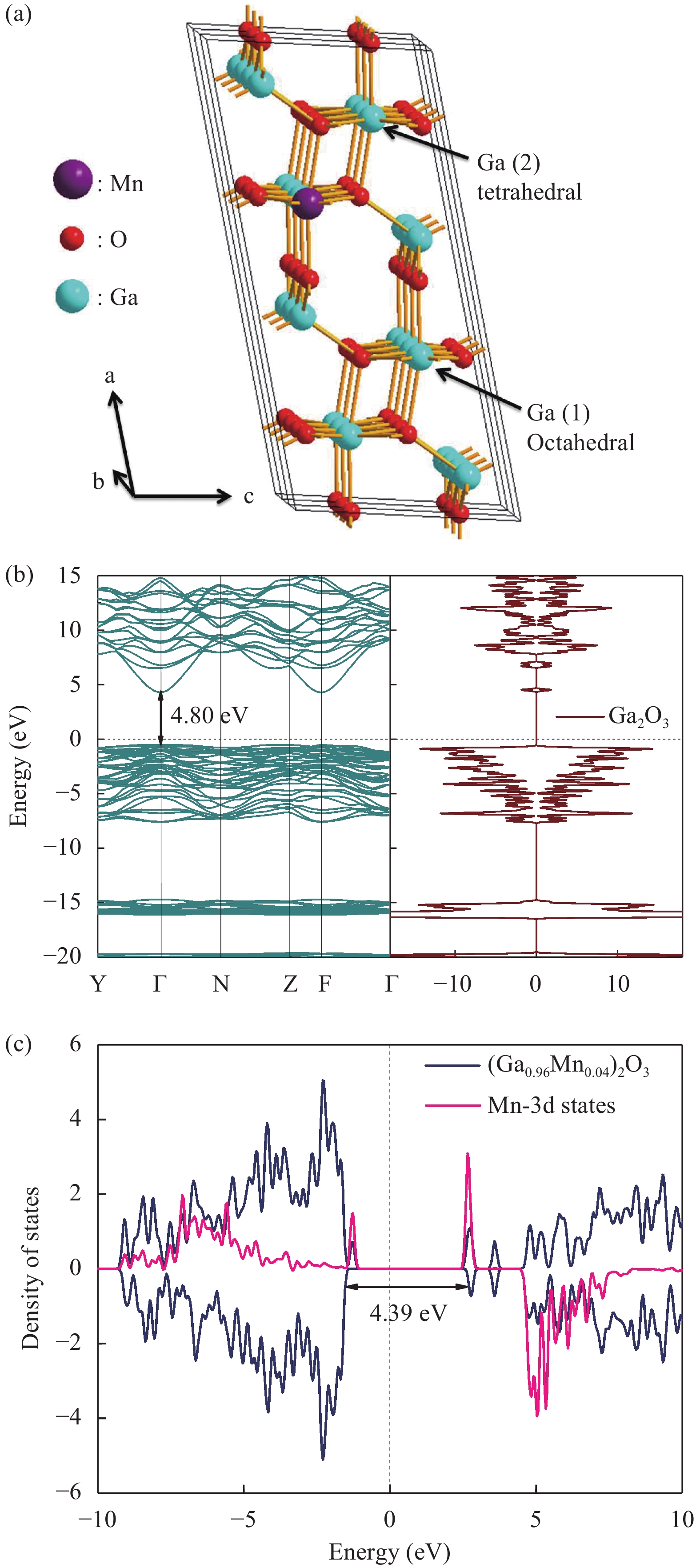
High quality epitaxial single phase (Ga0.96Mn0.04)2O3 and Ga2O3 thin films have been prepared on sapphire substrates by using laser molecular beam epitaxy (L-MBE). X-ray diffraction results indicate that the thin films have the monoclinic structure with a


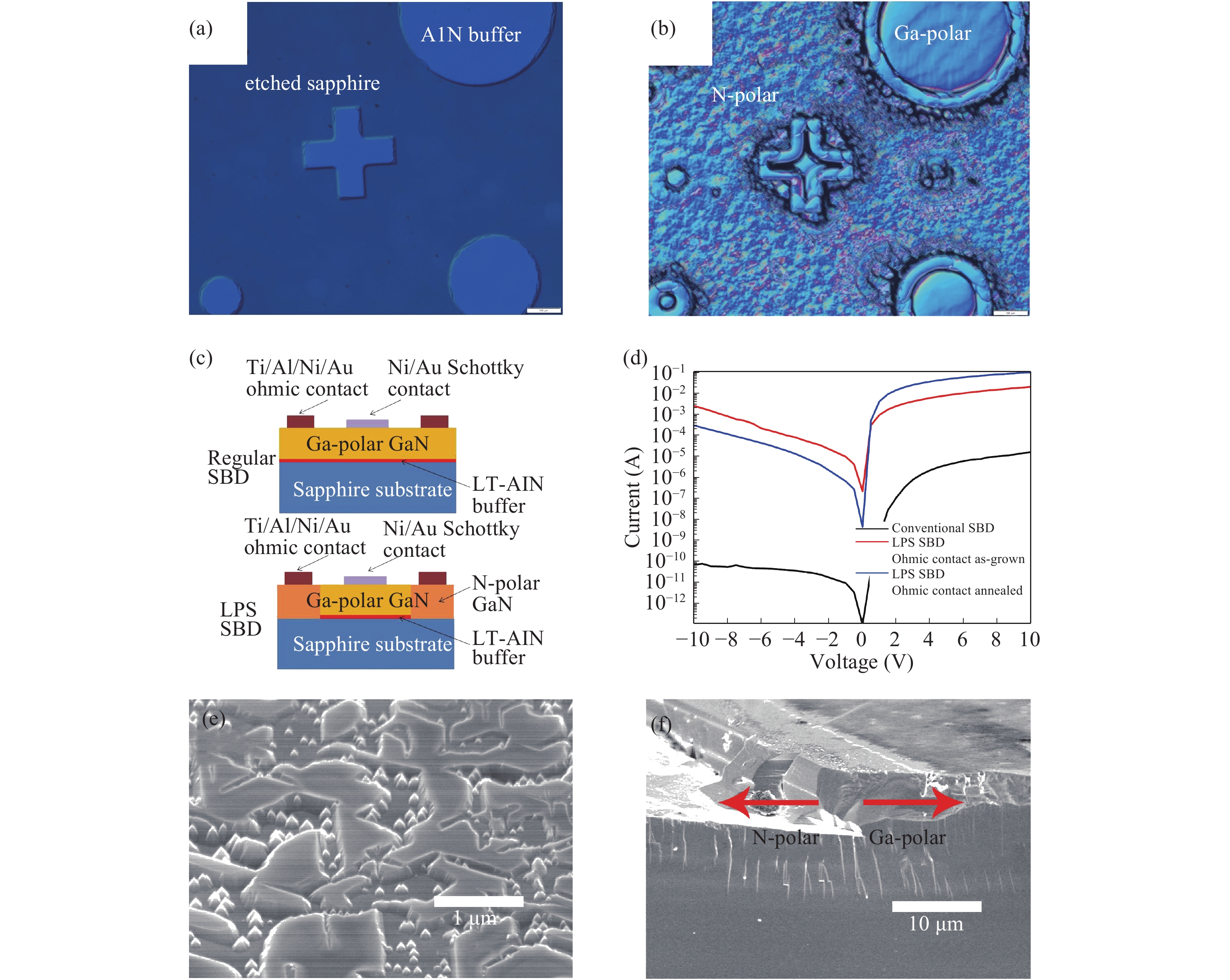
N-polar and III-polar GaN and AlN epitaxial thin films grown side by side on single sapphire substrate was reported. Surface morphology, wet etching susceptibility and bi-axial strain conditions were investigated and the polarity control scheme was utilized in the fabrication of Schottky barrier diode where ohmic contact and Schottky contact were deposited on N-polar domains and Ga-polar domains, respectively. The influence of N-polarity on on-state resistivity and I–V characteristic was discussed, demonstrating that lateral polarity structure of GaN and AlN can be widely used in new designs of optoelectronic and electronic devices.


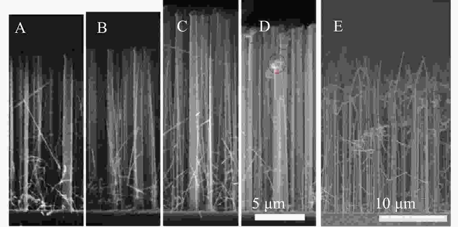
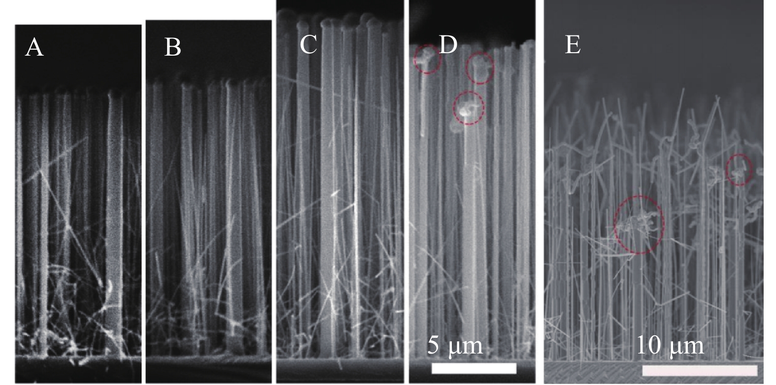
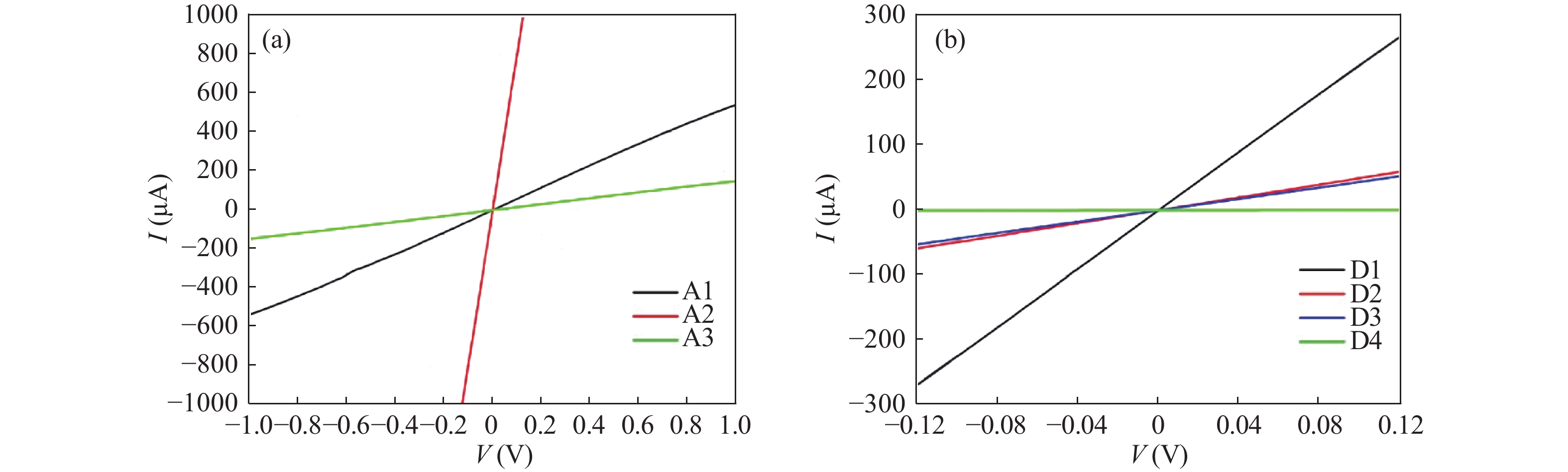
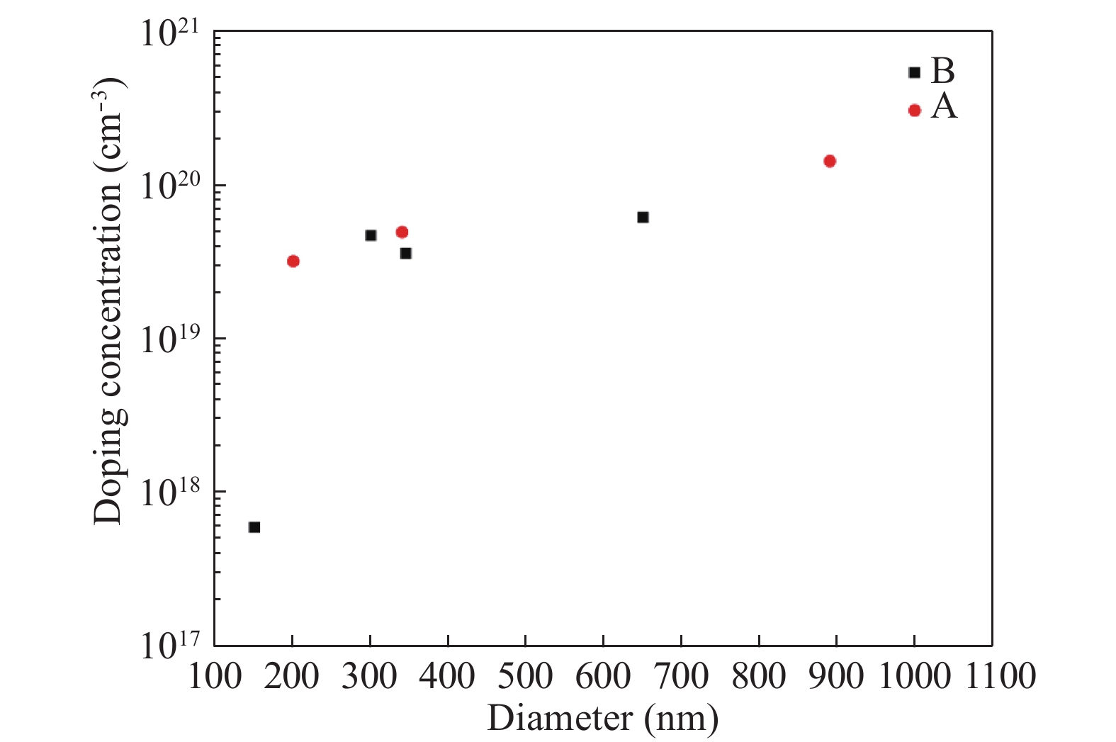
The growth of p-type GaAs nanowires (NWs) on GaAs (111) B substrates by metal-organic chemical vapor deposition (MOCVD) has been systematically investigated as a function of diethyl zinc (DEZn) flow. The growth rate of GaAs NWs was slightly improved by Zn-doping and kink is observed under high DEZn flow. In addition, the I–V curves of GaAs NWs has been measured and the p-type dope concentration under the II/III ratio of 0.013 and 0.038 approximated to 1019–1020 cm−3.


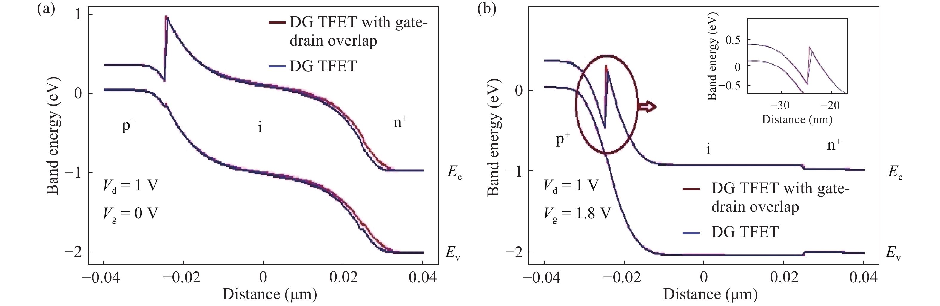
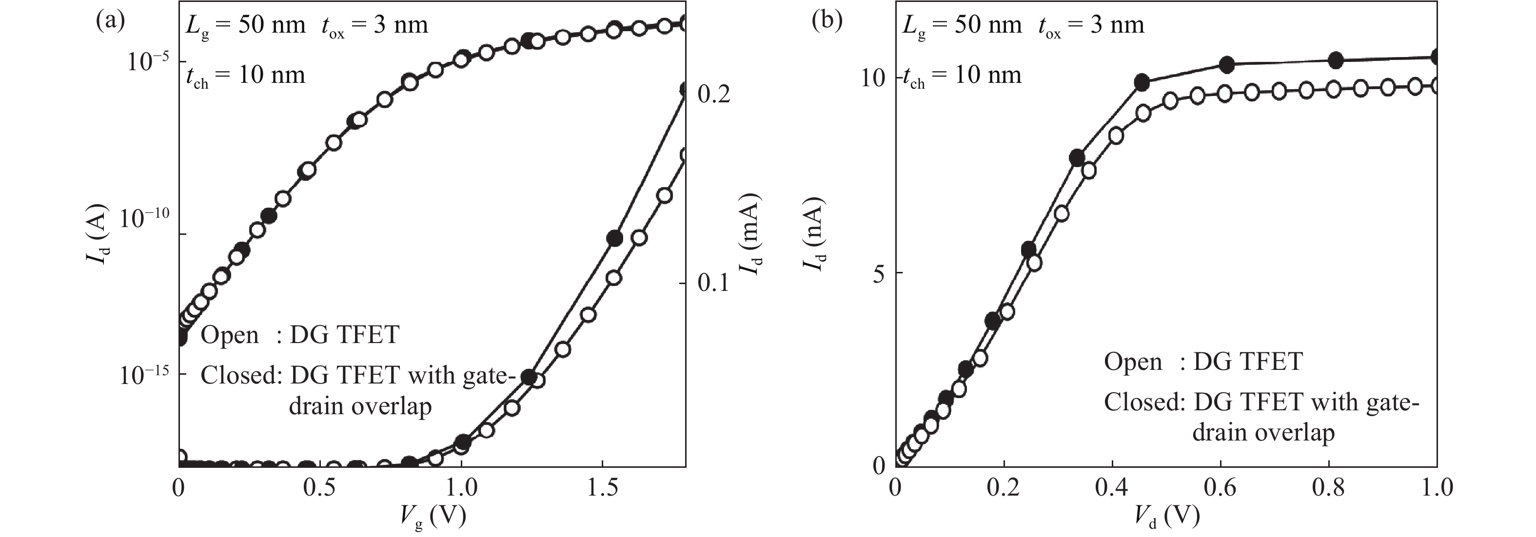
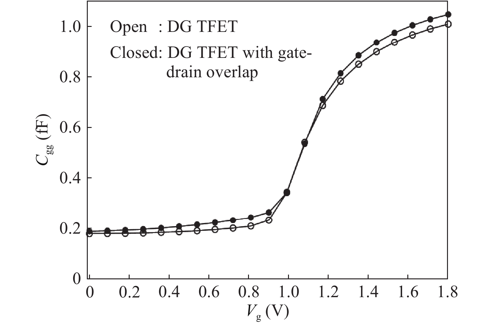
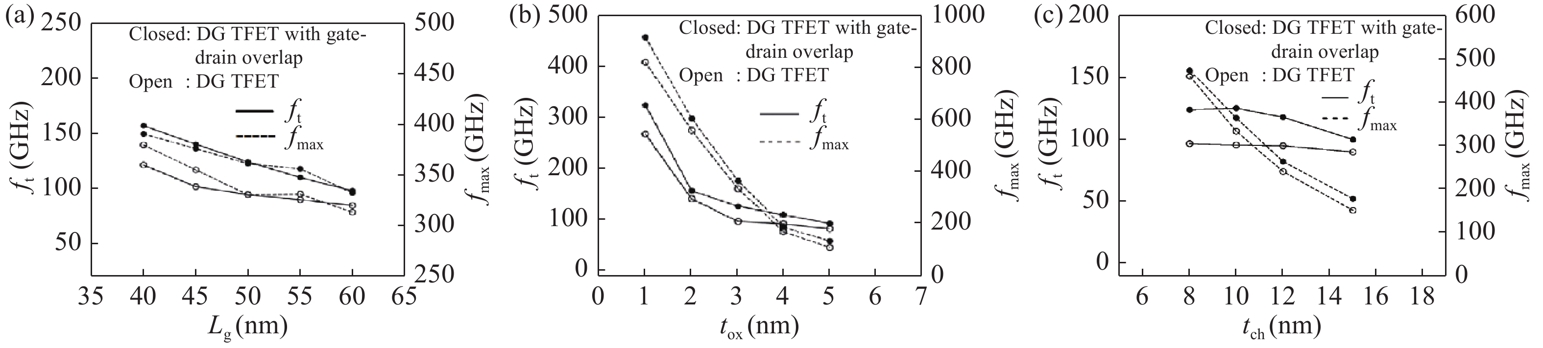
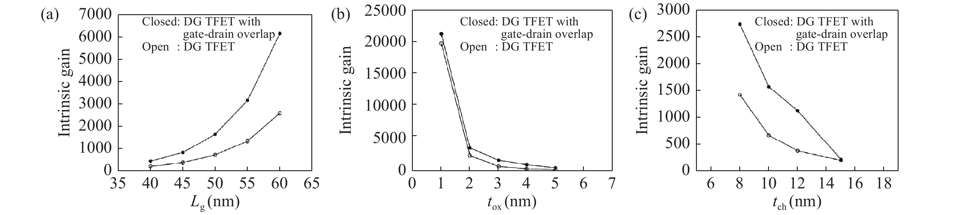
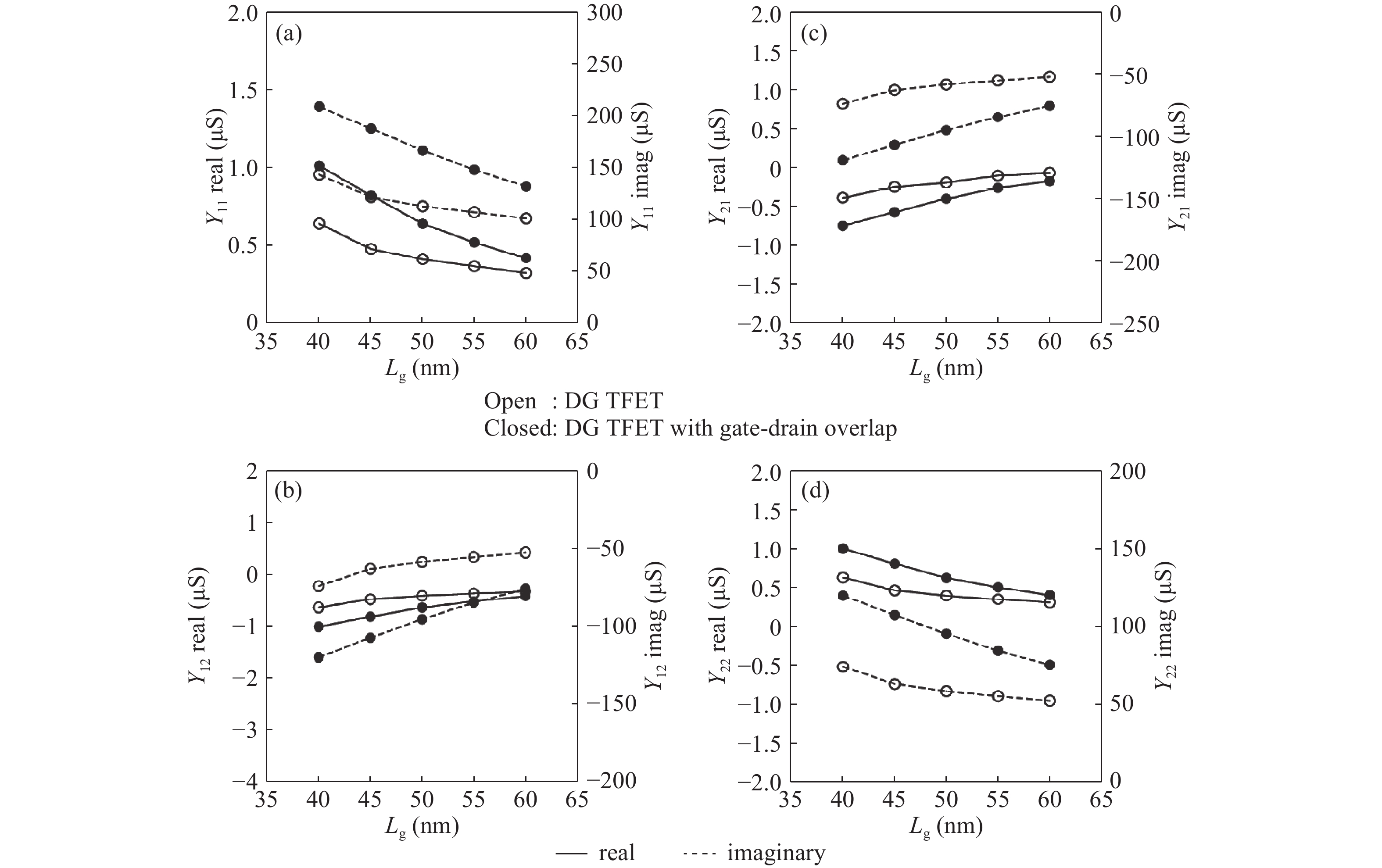
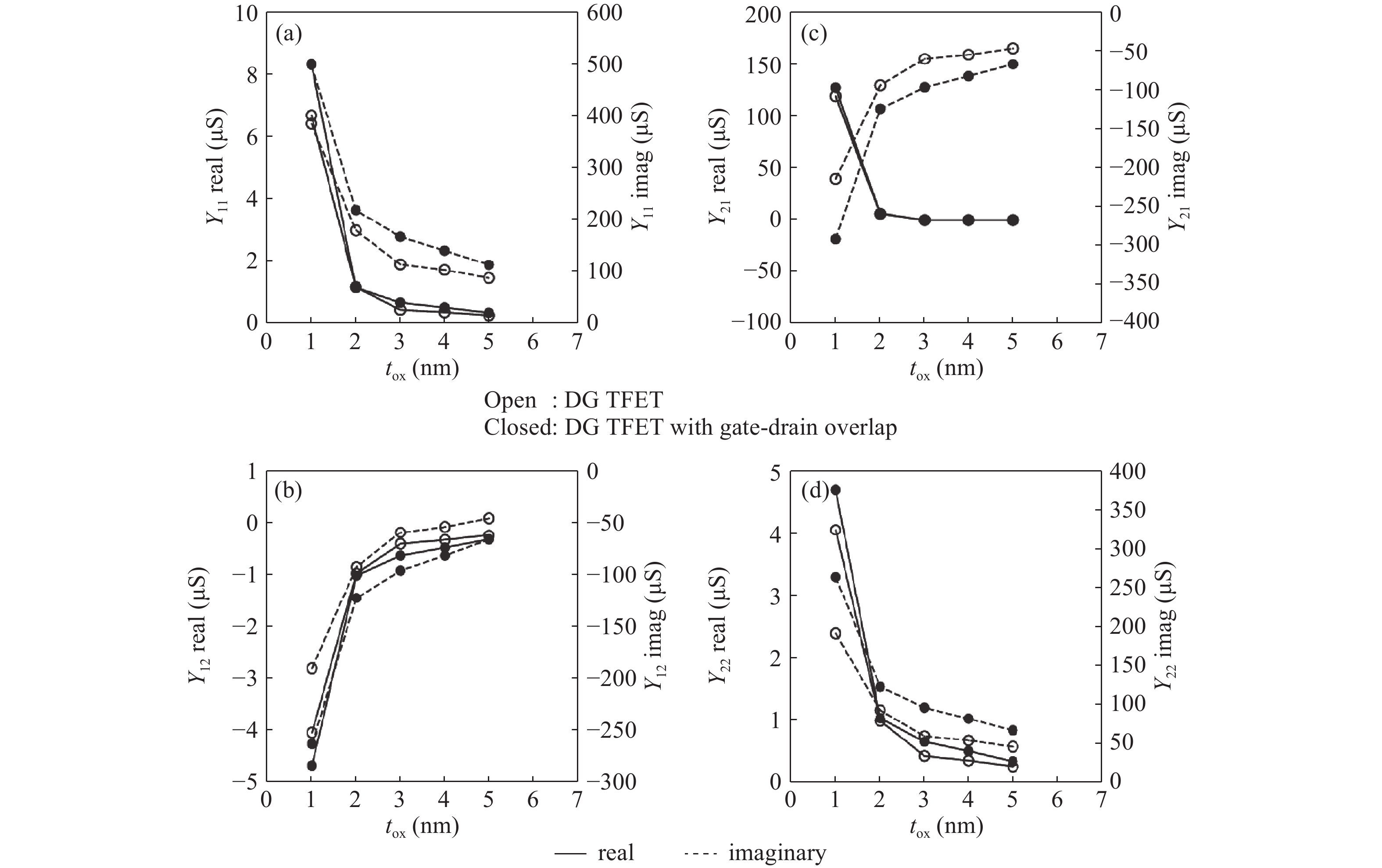
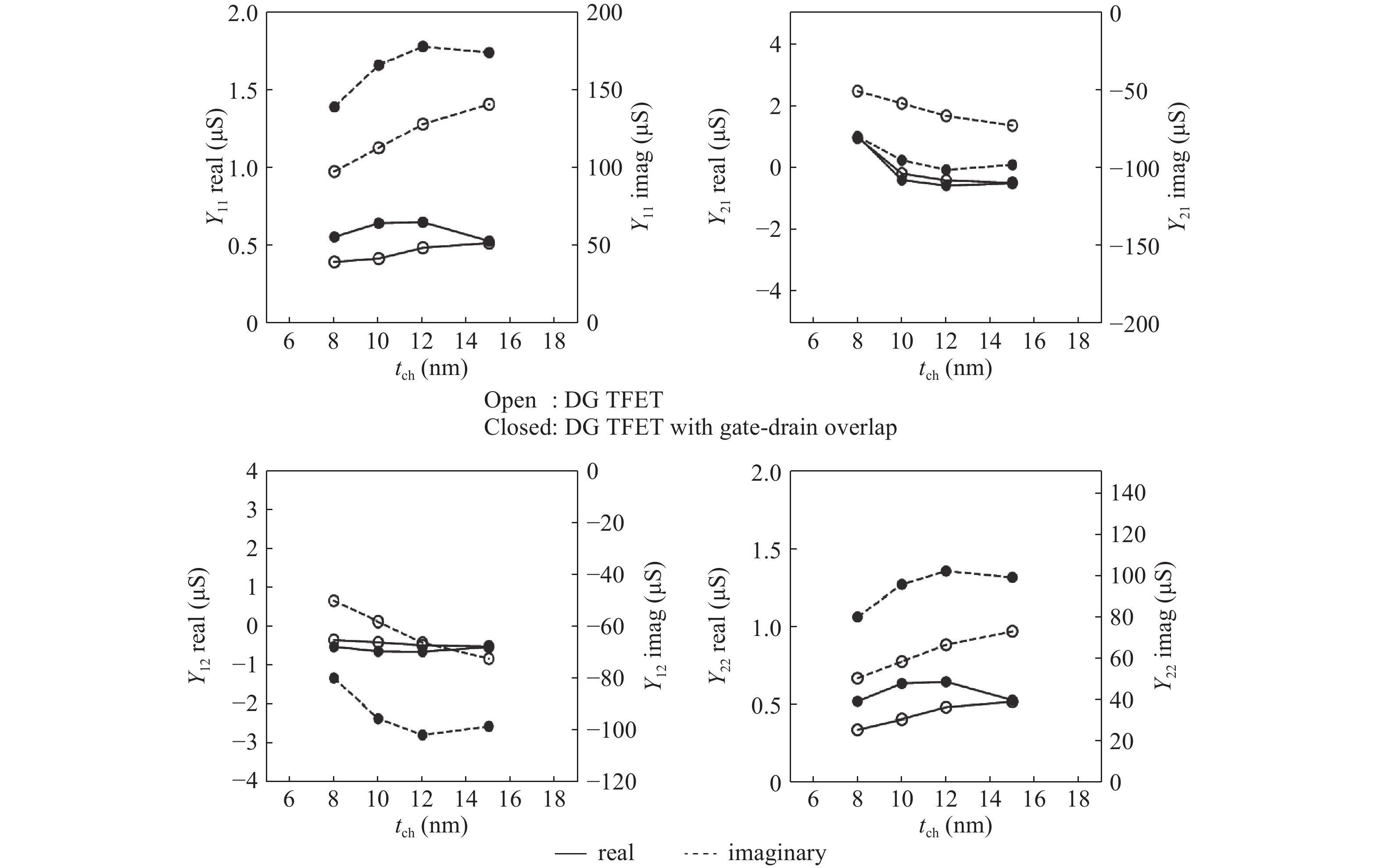
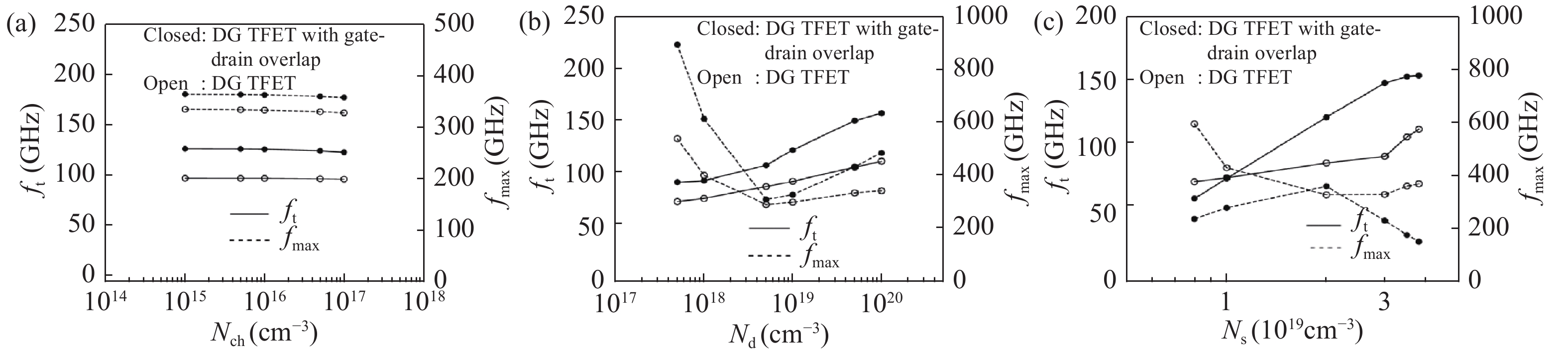
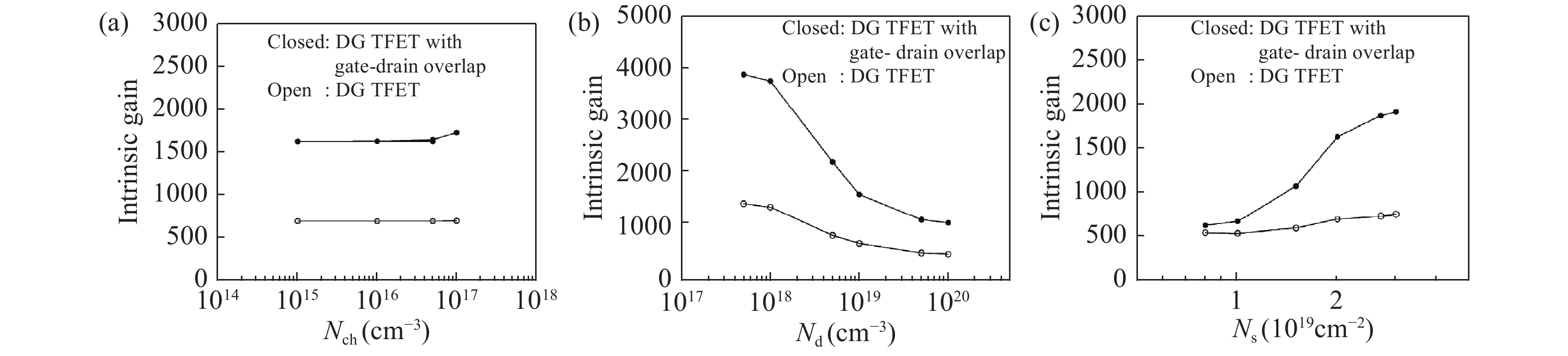
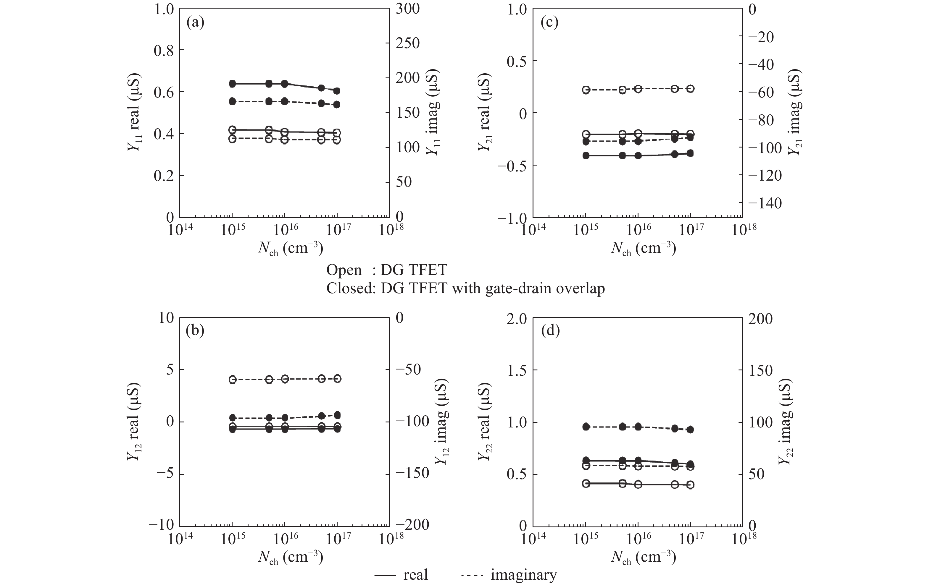
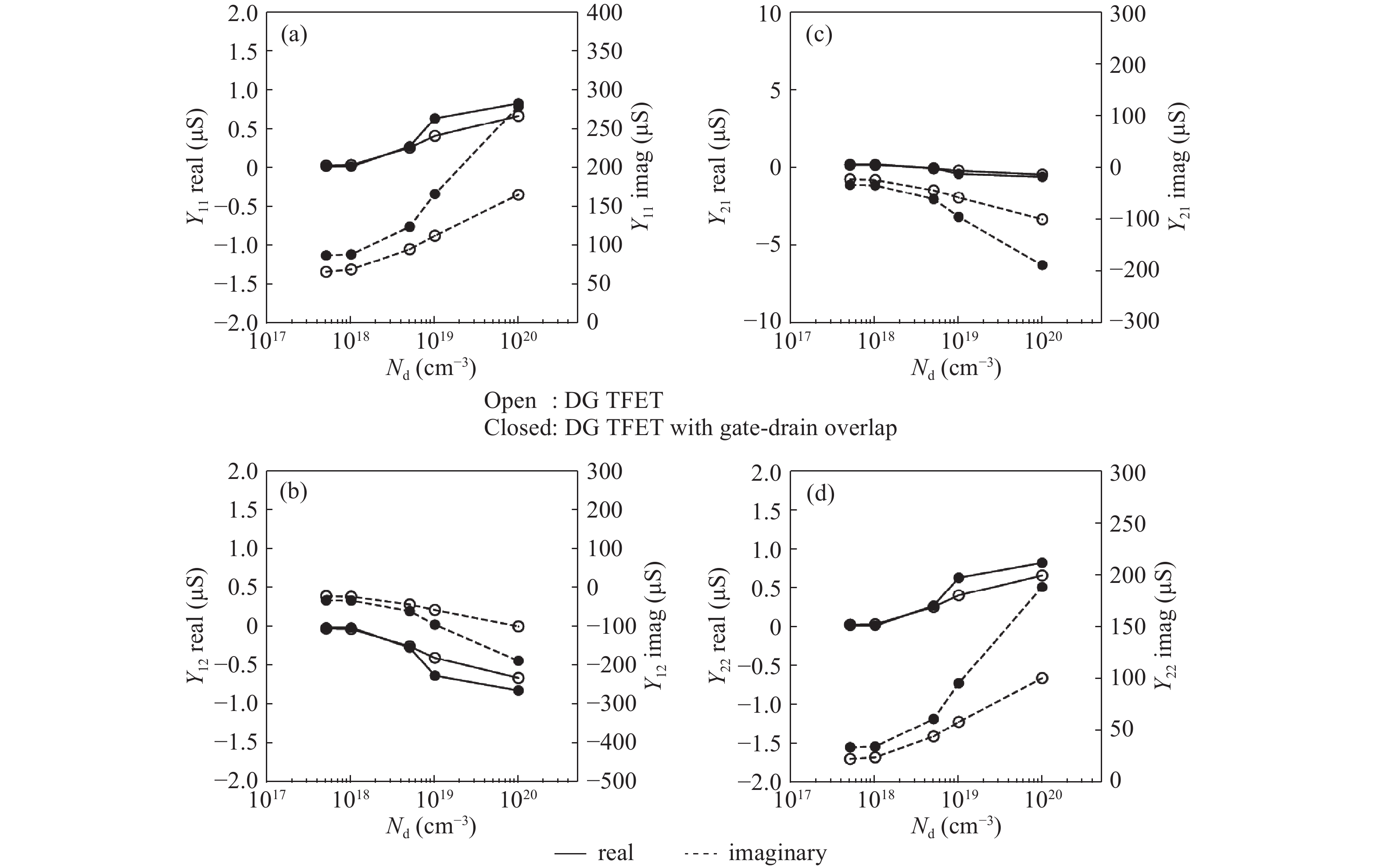
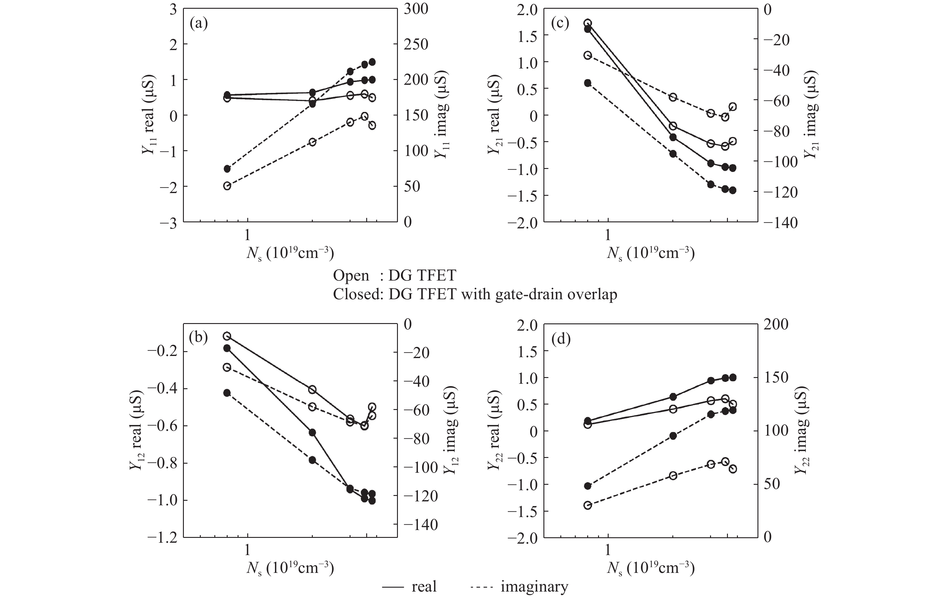
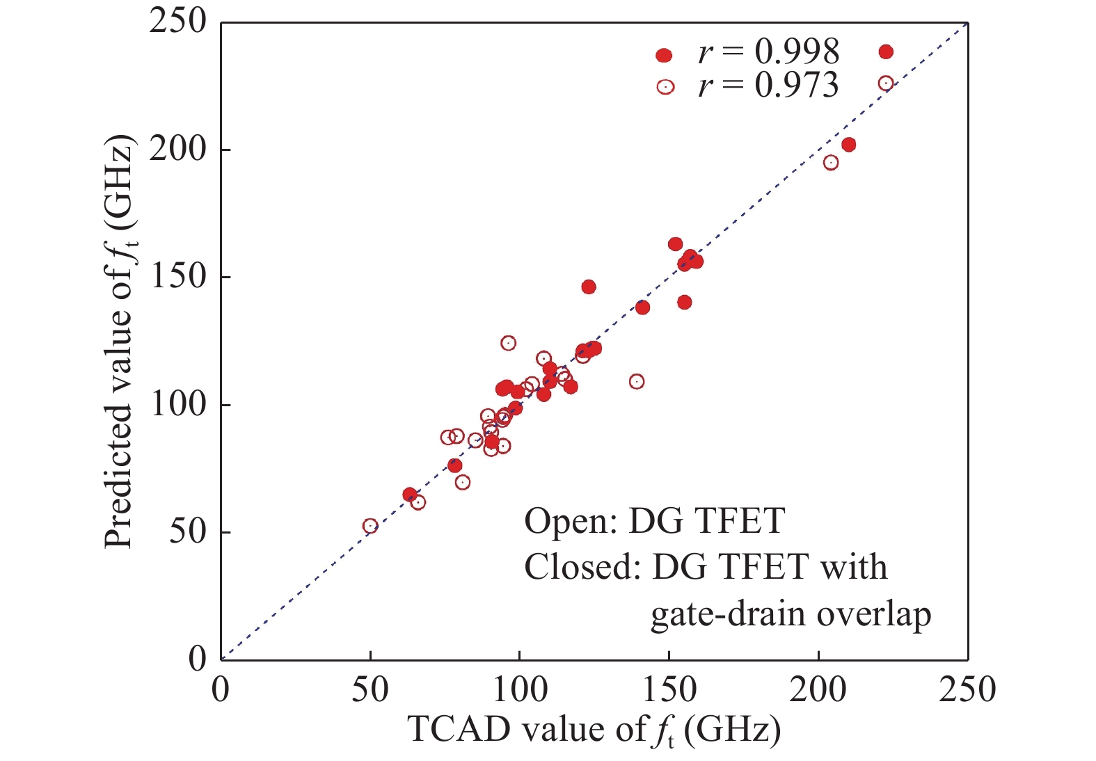
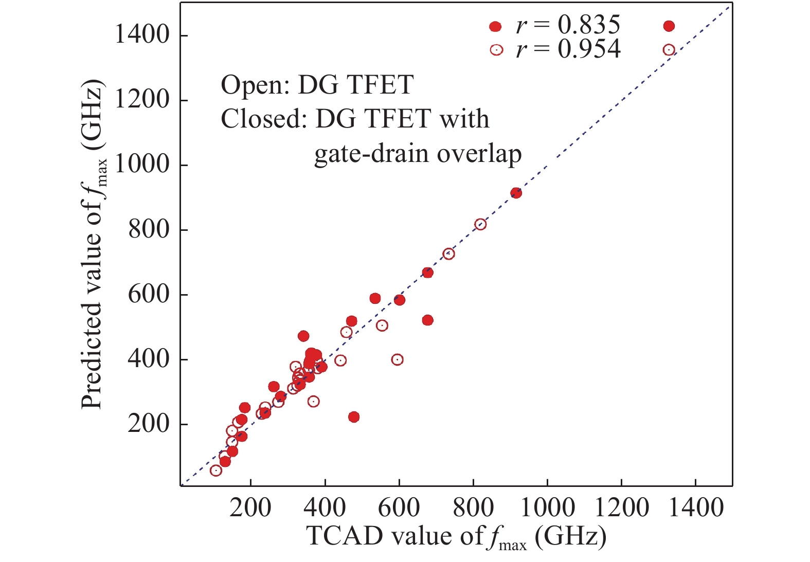
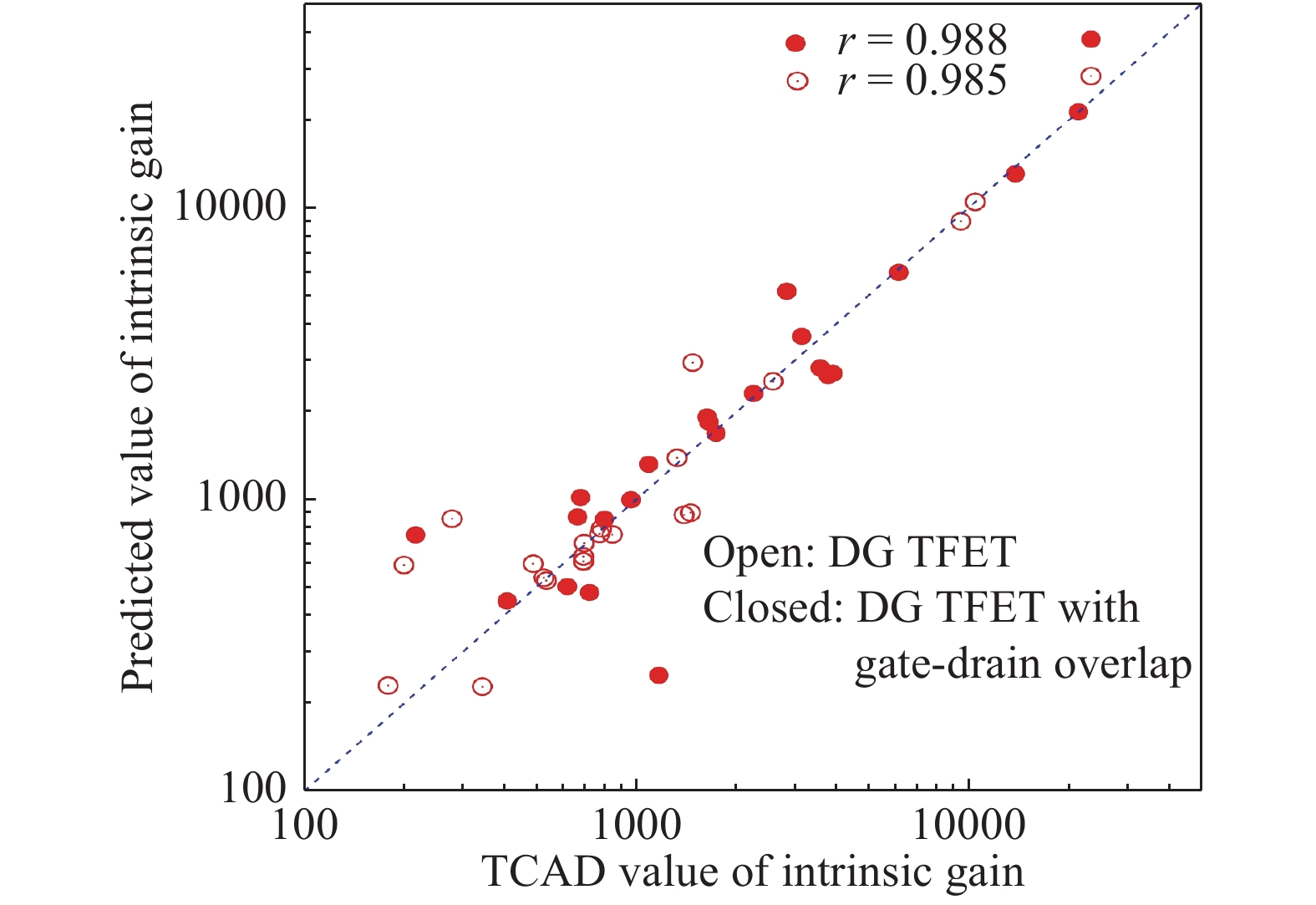
In this paper, RF performance analysis of InAs-based double gate (DG) tunnel field effect transistors (TFETs) is investigated in both qualitative and quantitative fashion. This investigation is carried out by varying the geometrical and doping parameters of TFETs to extract various RF parameters, unity gain cut-off frequency (ft), maximum oscillation frequency (fmax), intrinsic gain and admittance (Y) parameters. An asymmetric gate oxide is introduced in the gate-drain overlap and compared with that of DG TFETs. Higher ON-current (ION) of about 0.2 mA and less leakage current (IOFF) of 29 fA is achieved for DG TFET with gate-drain overlap. Due to increase in transconductance (gm), higher ft and intrinsic gain is attained for DG TFET with gate-drain overlap. Higher fmax of 985 GHz is obtained for drain doping of 5 × 1017 cm−3 because of the reduced gate-drain capacitance (Cgd) with DG TFET with gate-drain overlap. In terms of Y-parameters, gate oxide thickness variation offers better performance due to the reduced values of Cgd. A second order numerical polynomial model is generated for all the RF responses as a function of geometrical and doping parameters. The simulation results are compared with this numerical model where the predicted values match with the simulated values.


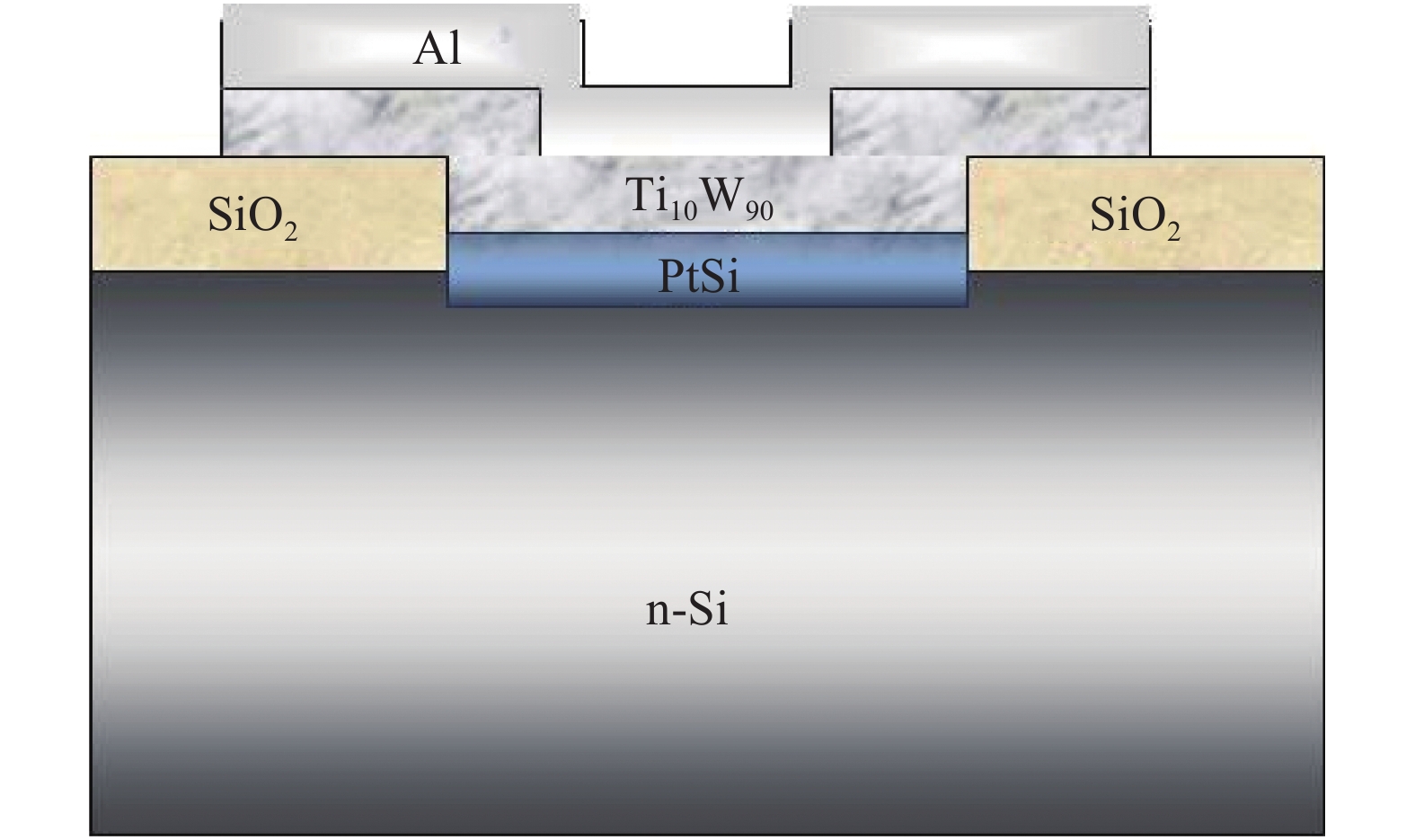
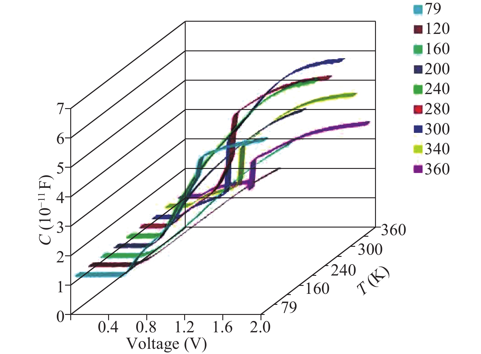
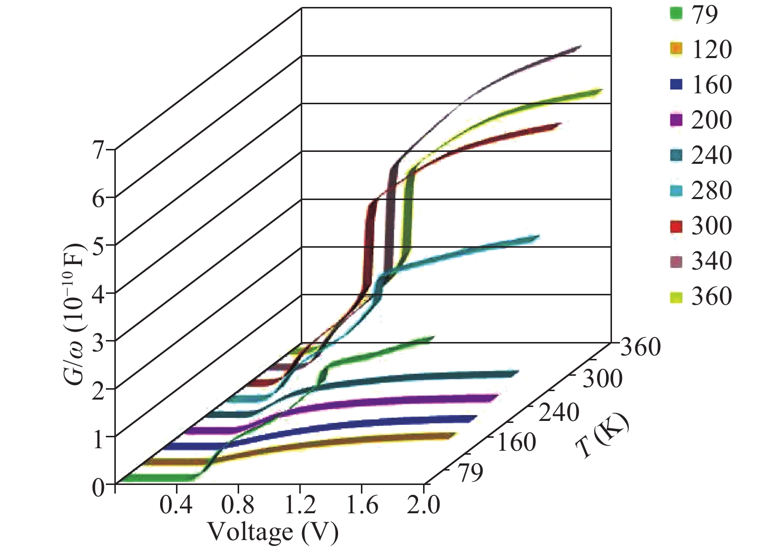
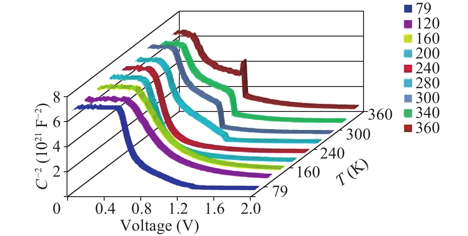
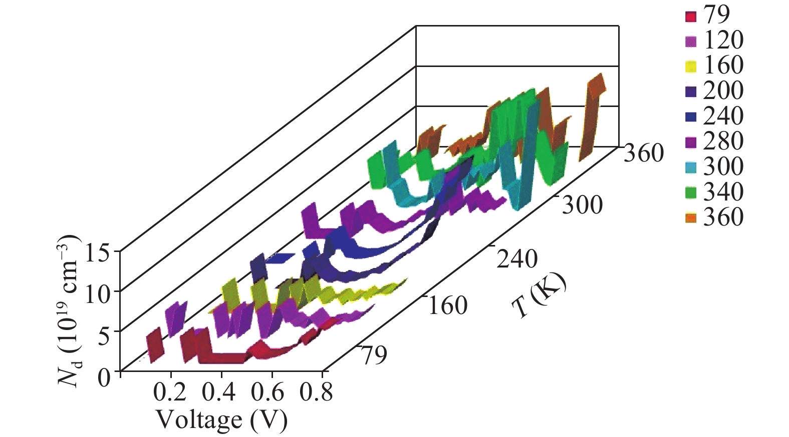
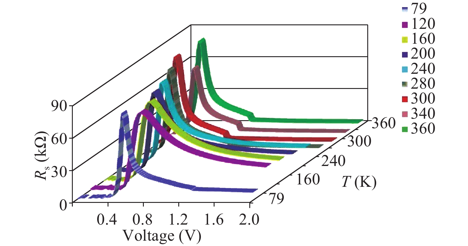
Using the effect of the temperature on the capacitance–voltage (C–V) and conductance–voltage (G/ω–V) characteristics of PtSi/n-Si (111) Schottky diodes the profile of apparent doping concentration (NDapp), the potential difference between the Fermi energy level and the bottom of the conduction band (Vn), apparent barrier height (ΦBapp), series resistance (Rs) and the interface state density Nss have been investigated. From the temperature dependence of (C–V) it was found that these parameters are non-uniformly changed with increasing temperature in a wide temperature range of 79–360 K. The voltage and temperature dependences of apparent carrier distribution we attributed to the existence of self-assembled patches similar the quantum wells, which formed due to the process of PtSi formation on semiconductor and the presence of hexagonal voids of Si (111).


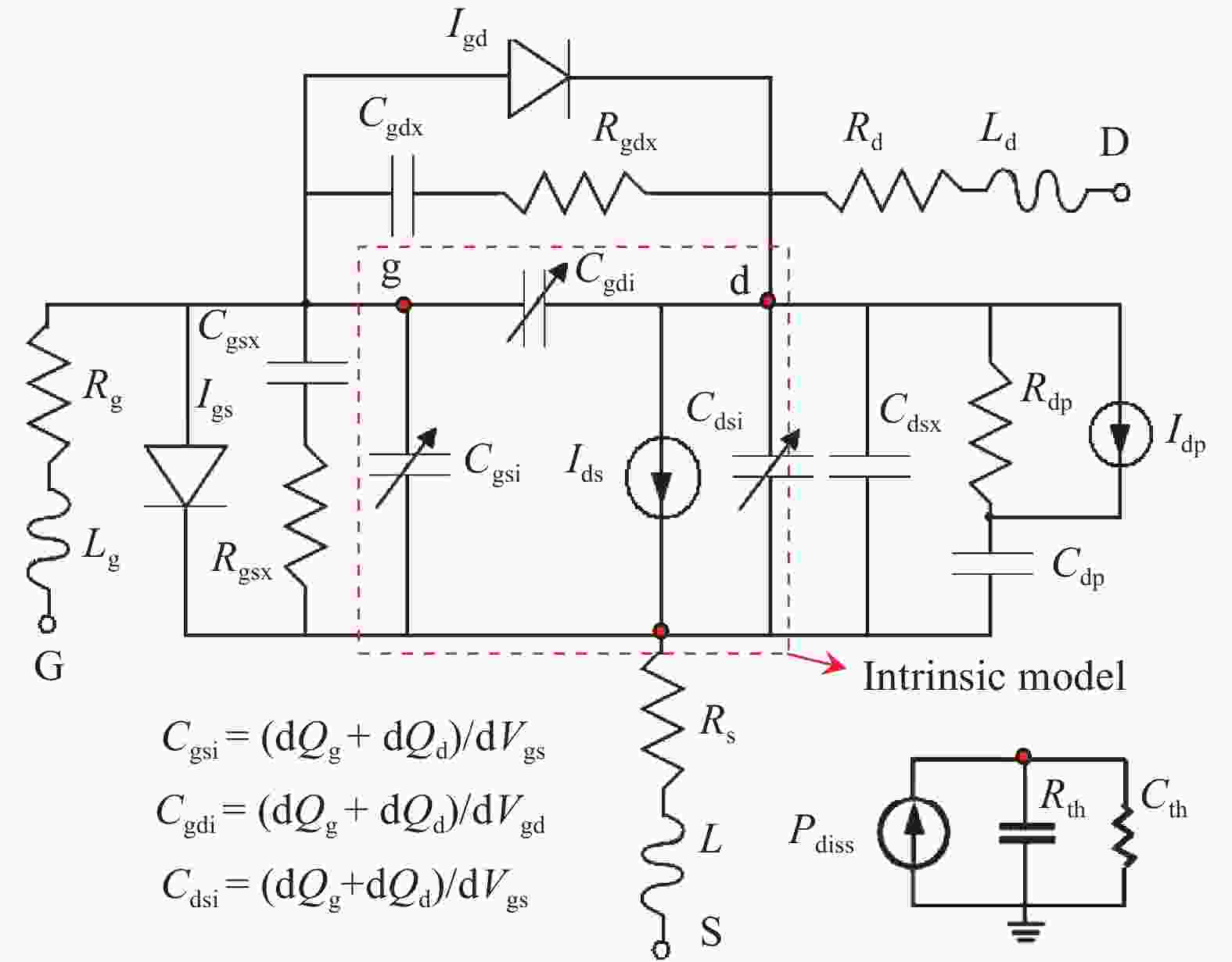
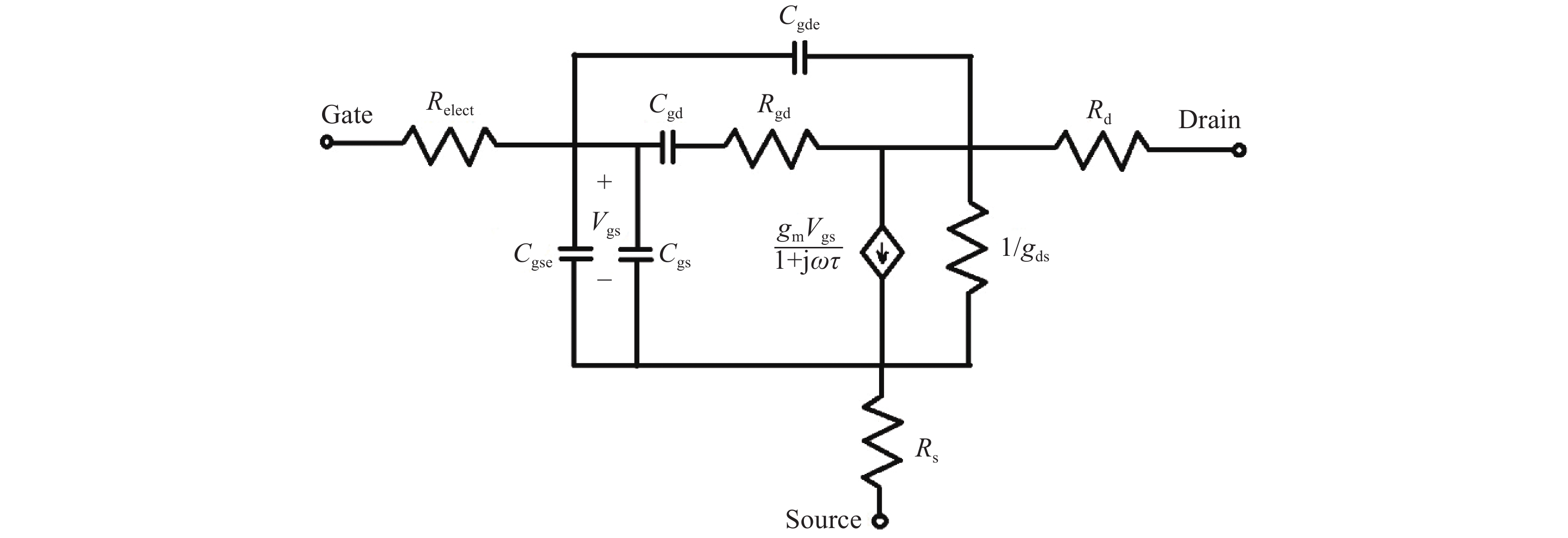
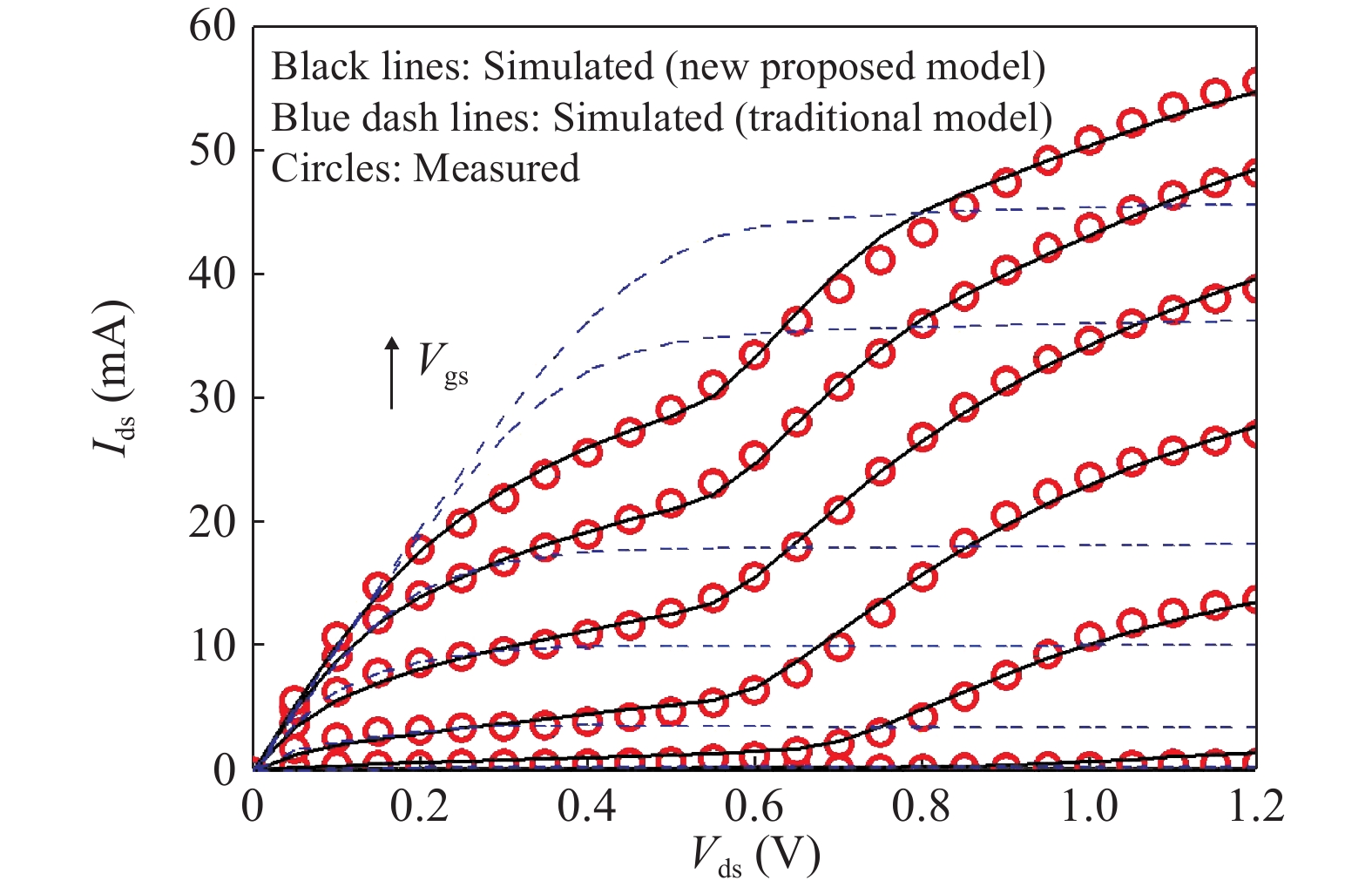
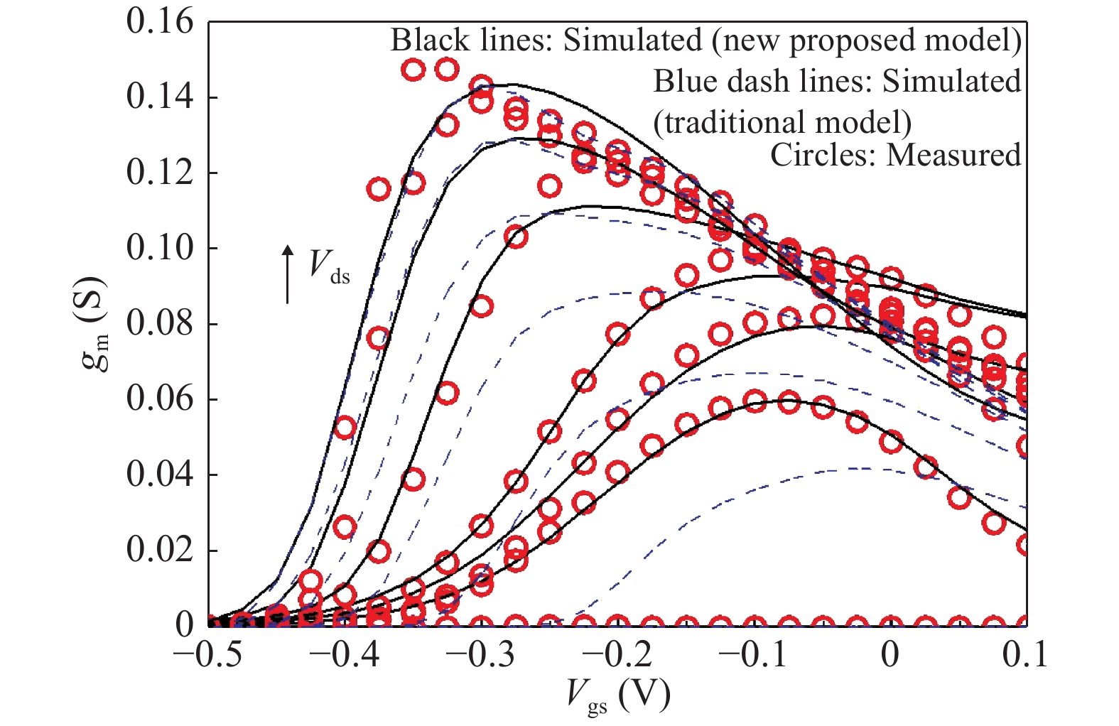
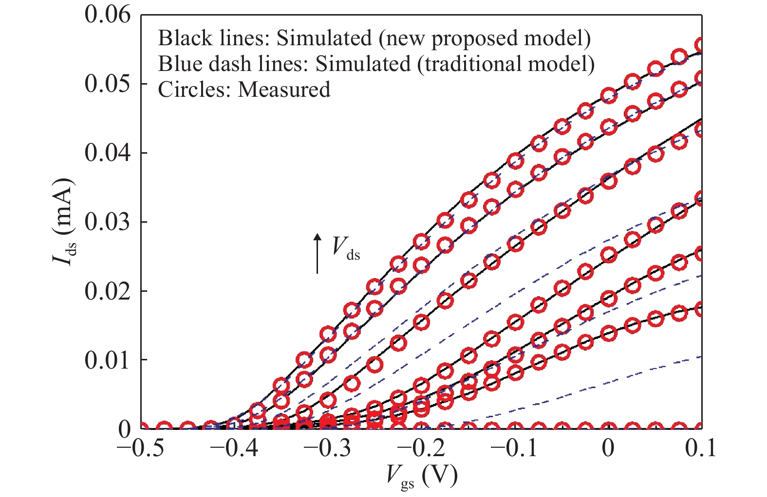
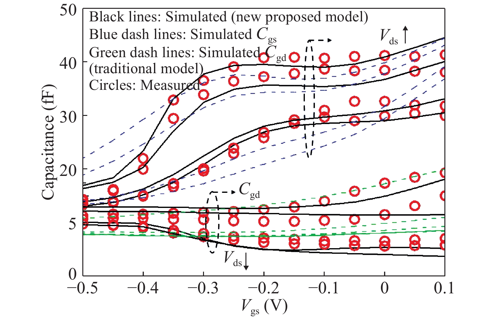
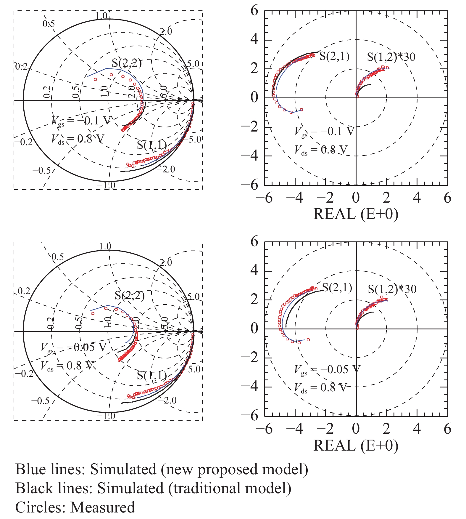
An improved large signal model for InP HEMTs is proposed in this paper. The channel current and charge model equations are constructed based on the Angelov model equations. Both the equations for channel current and gate charge models were all continuous and high order drivable, and the proposed gate charge model satisfied the charge conservation. For the strong leakage induced barrier reduction effect of InP HEMTs, the Angelov current model equations are improved. The channel current model could fit DC performance of devices. A 2 × 25 μm × 70 nm InP HEMT device is used to demonstrate the extraction and validation of the model, in which the model has predicted the DC I–V, C–V and bias related S parameters accurately.


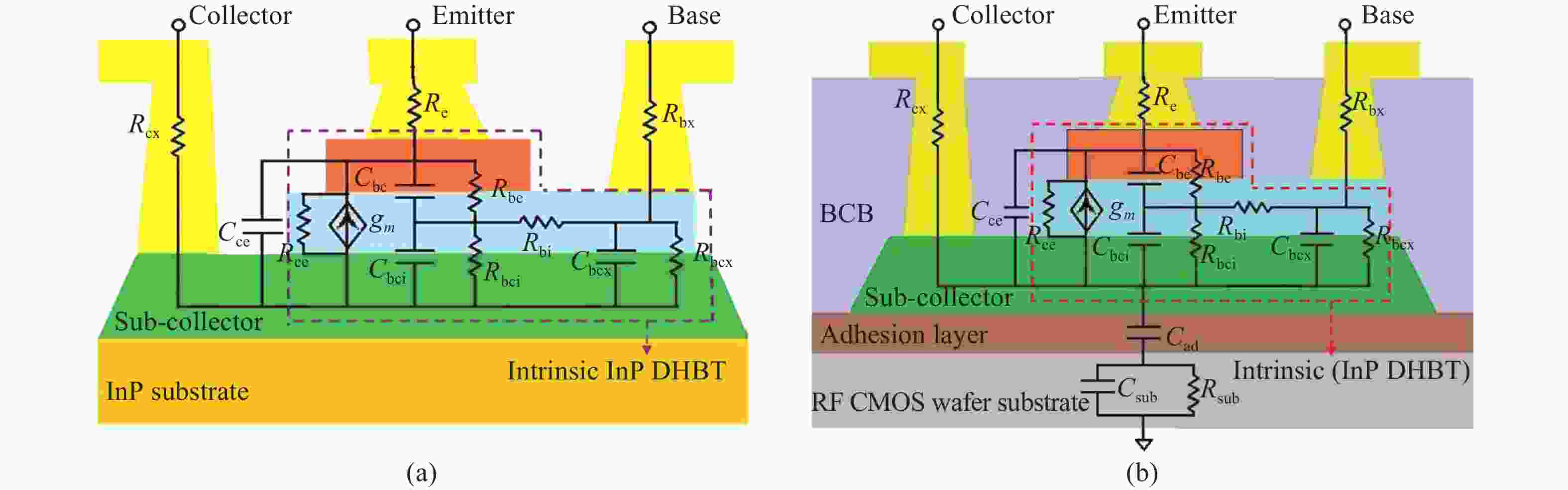
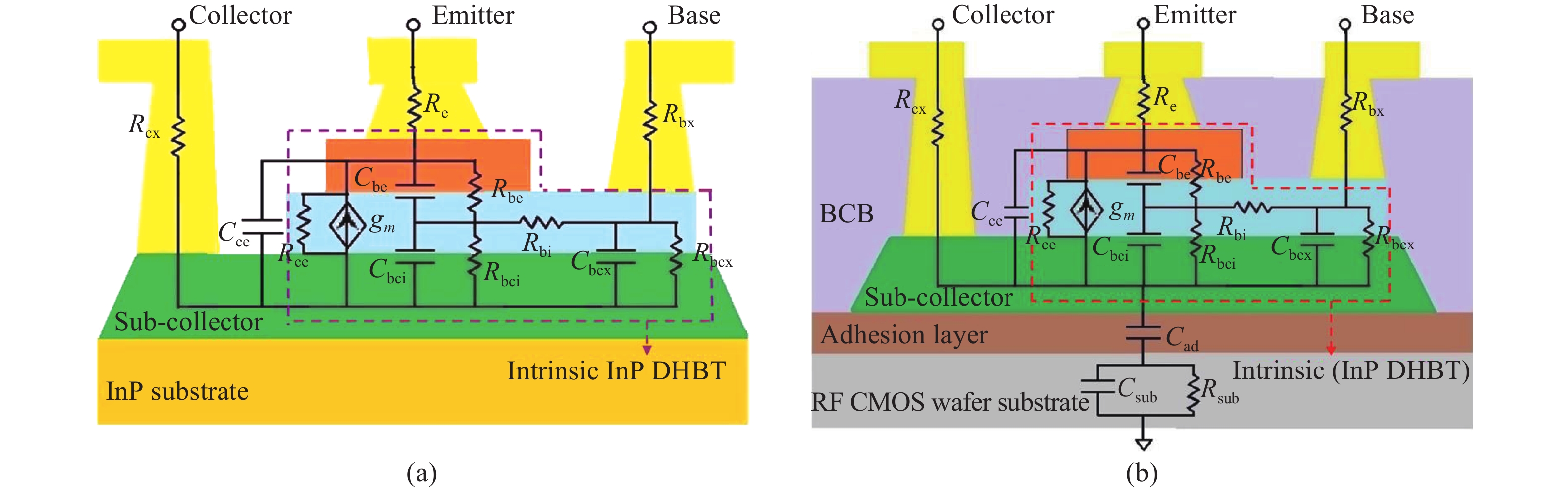
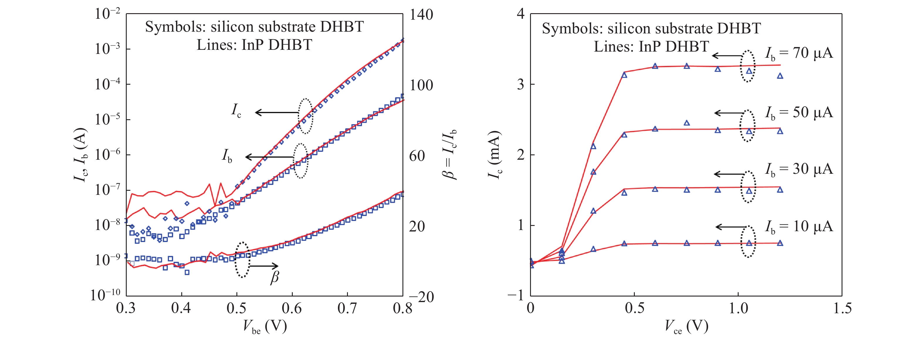
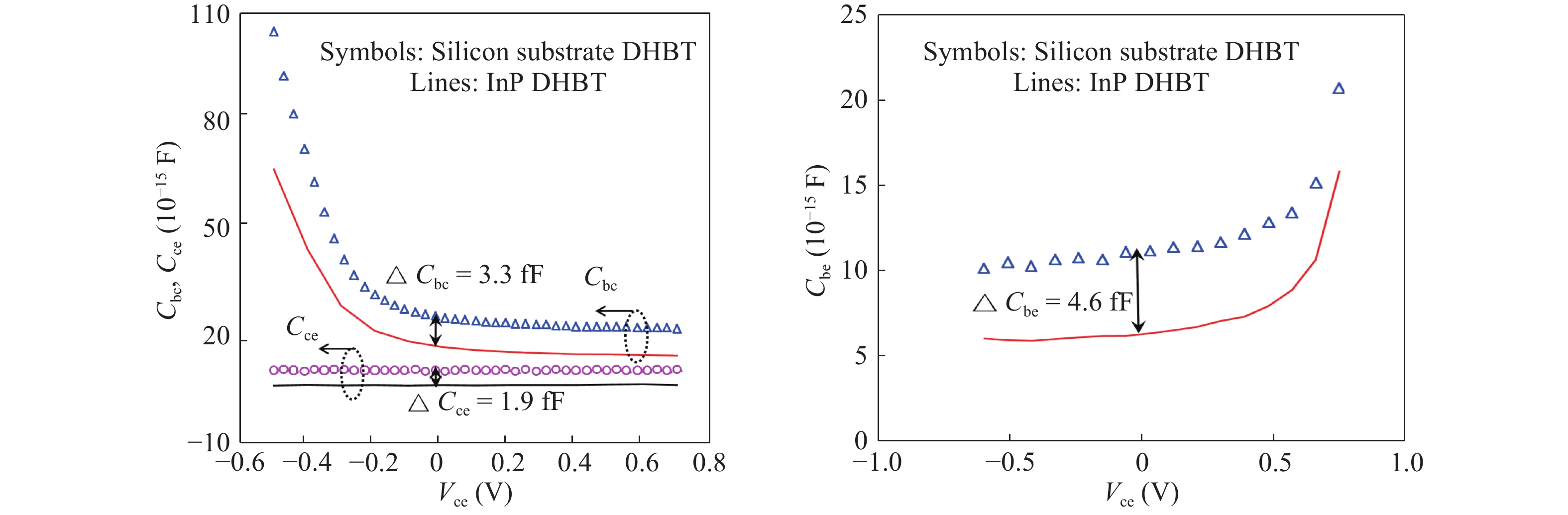
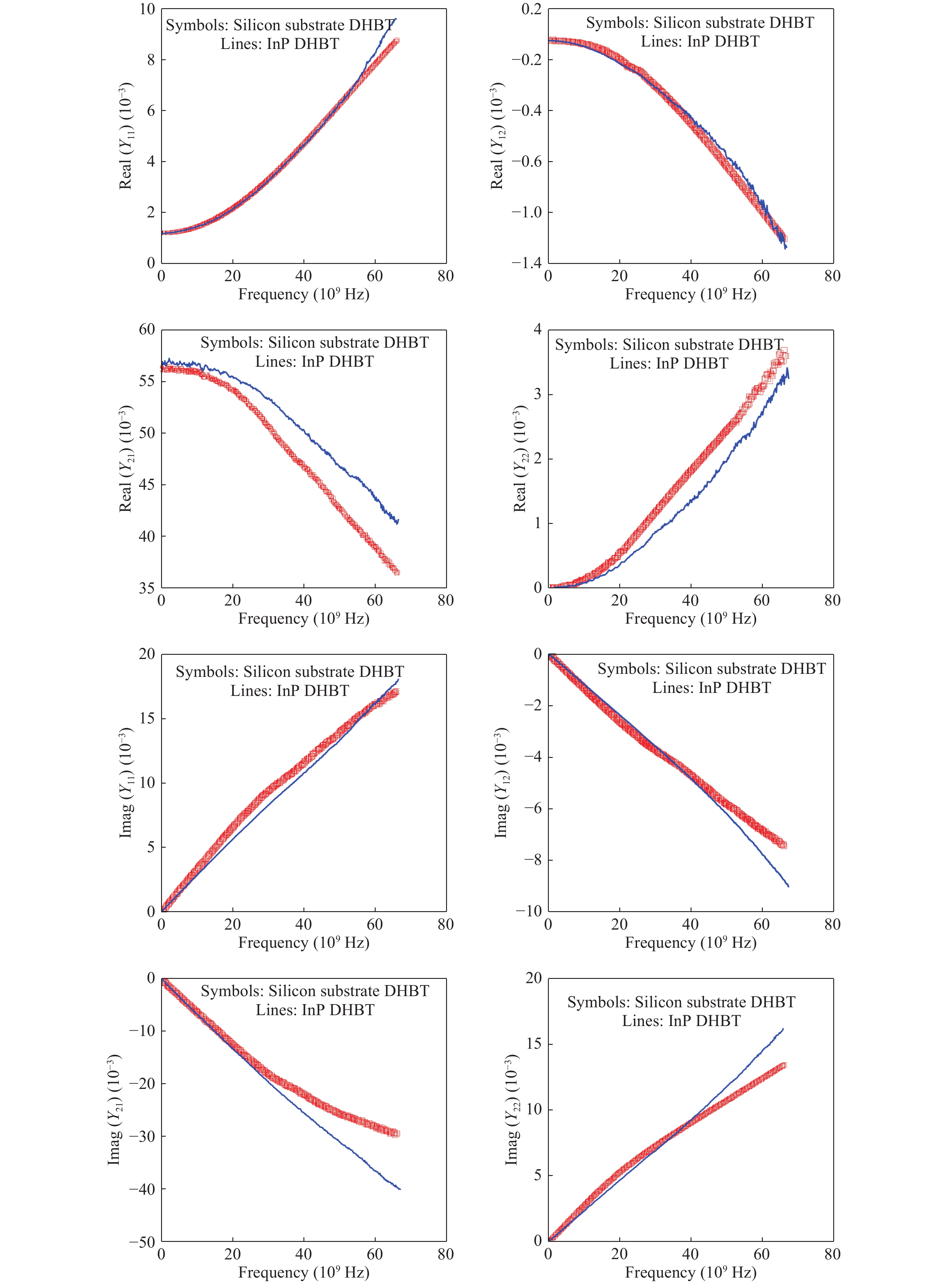
This paper investigated the DC and RF performance of the InP double heterojunction bipolar transistors (DHBTs) transferred to RF CMOS wafer substrate. The measurement results show that the maximum values of the DC current gain of a substrate transferred device had one emitter finger, of 0.8 μm in width and 5 μm in length, are changed unobviously, while the cut-off frequency and the maximum oscillation frequency are decreased from 220 to 171 GHz and from 204 to 154 GHz, respectively. In order to have a detailed insight on the degradation of the RF performance, small-signal models for the InP DHBT before and after substrate transferred are presented and comparably extracted. The extracted results show that the degradation of the RF performance of the device transferred to RF CMOS wafer substrate are mainly caused by the additional introduced substrate parasitics and the increase of the capacitive parasitics induced by the substrate transfer process itself.

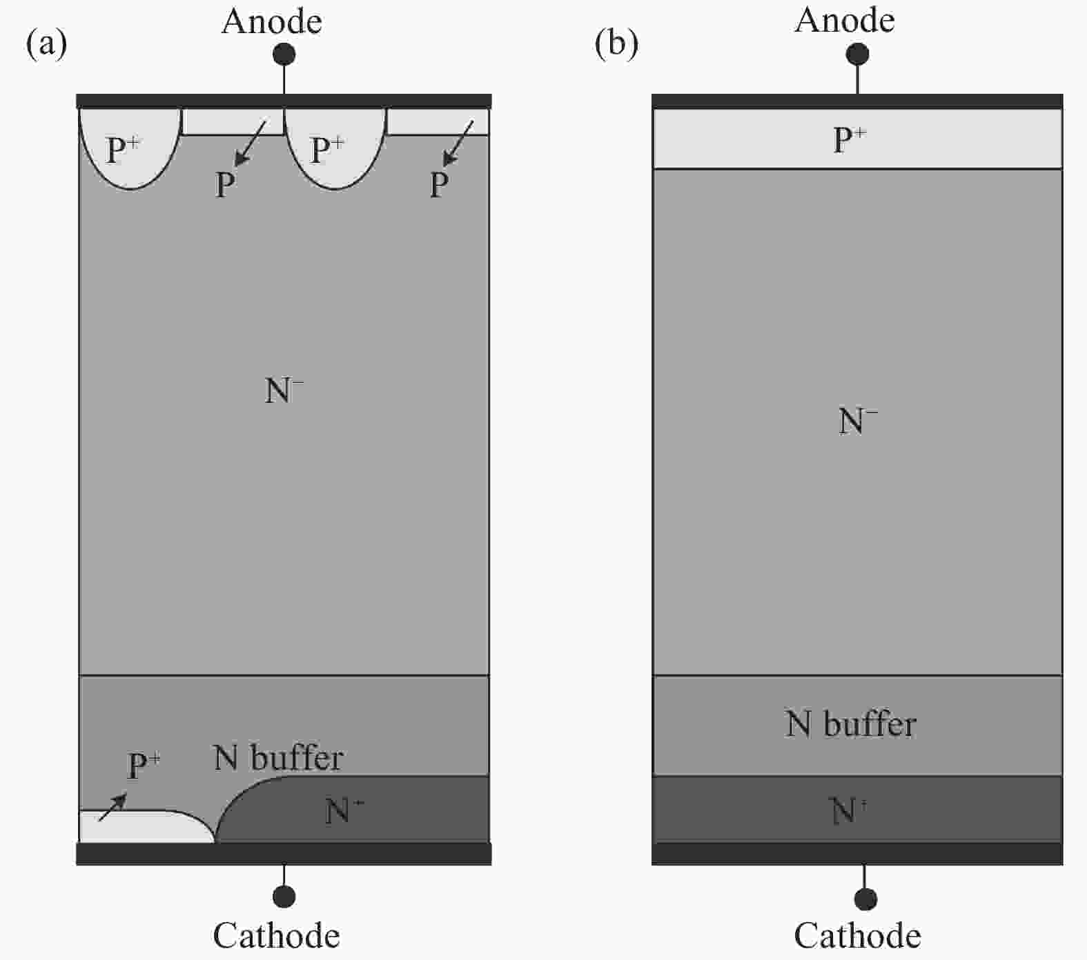
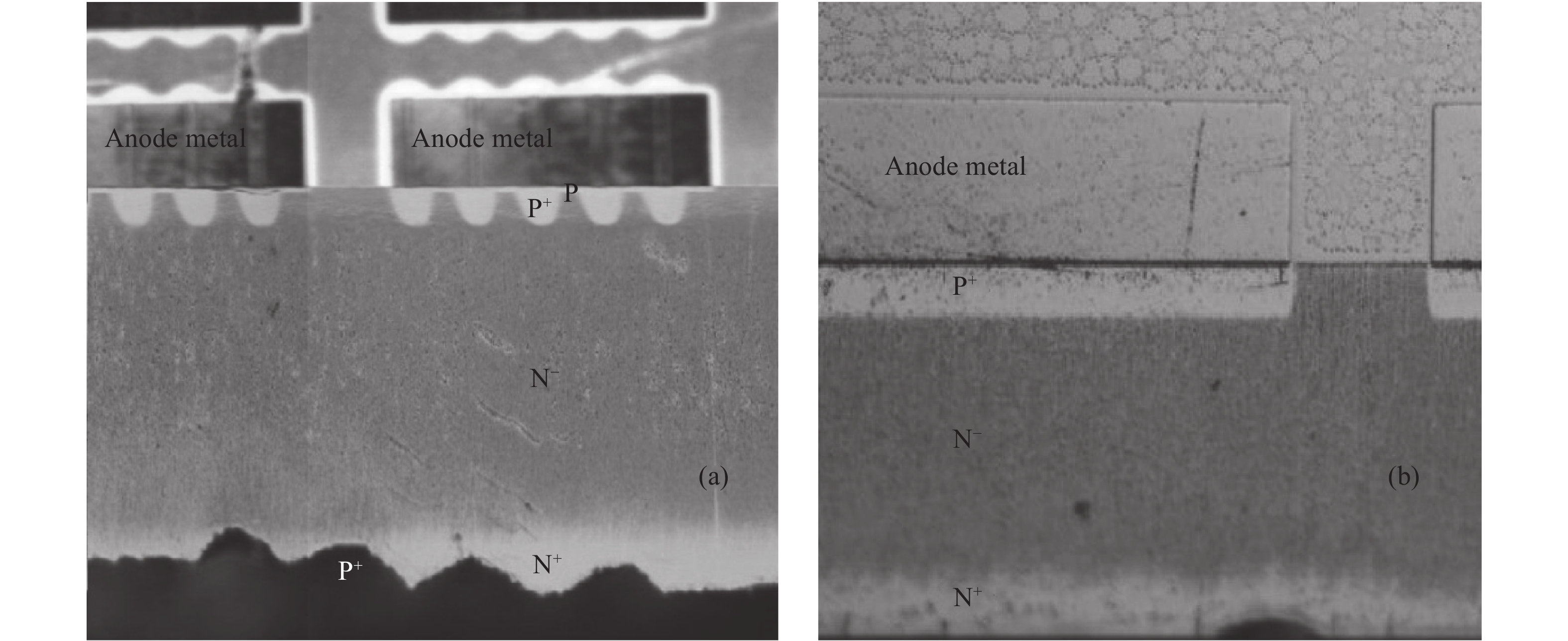
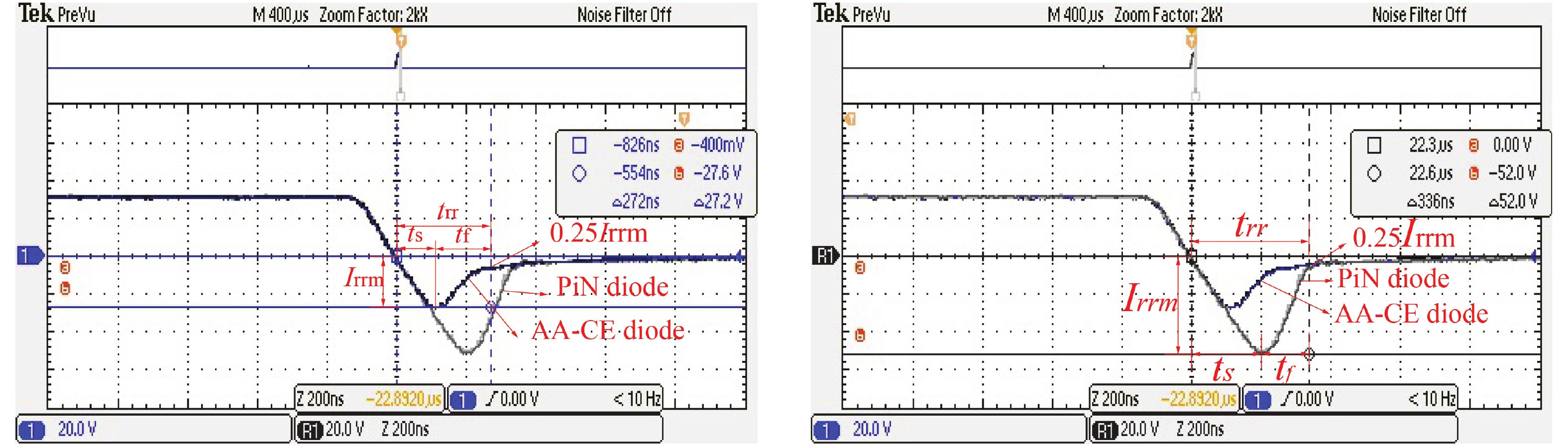
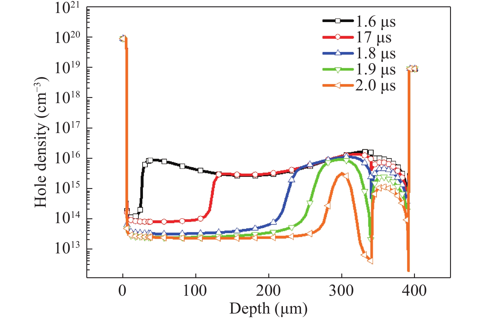
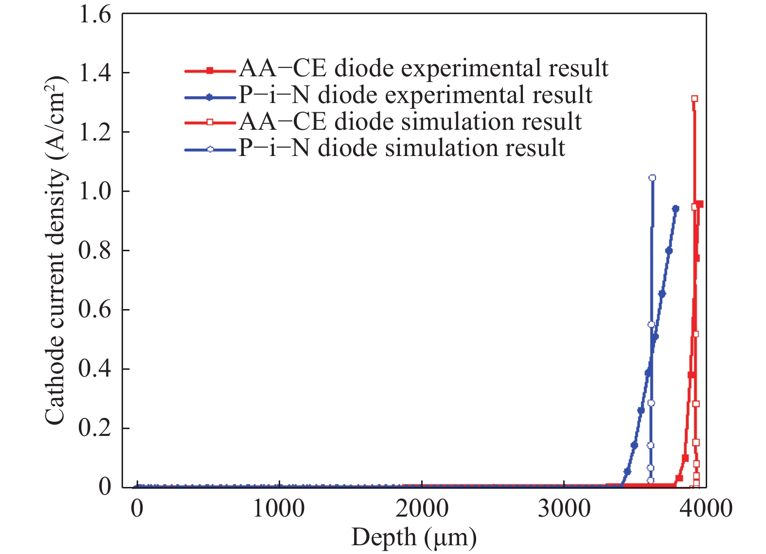
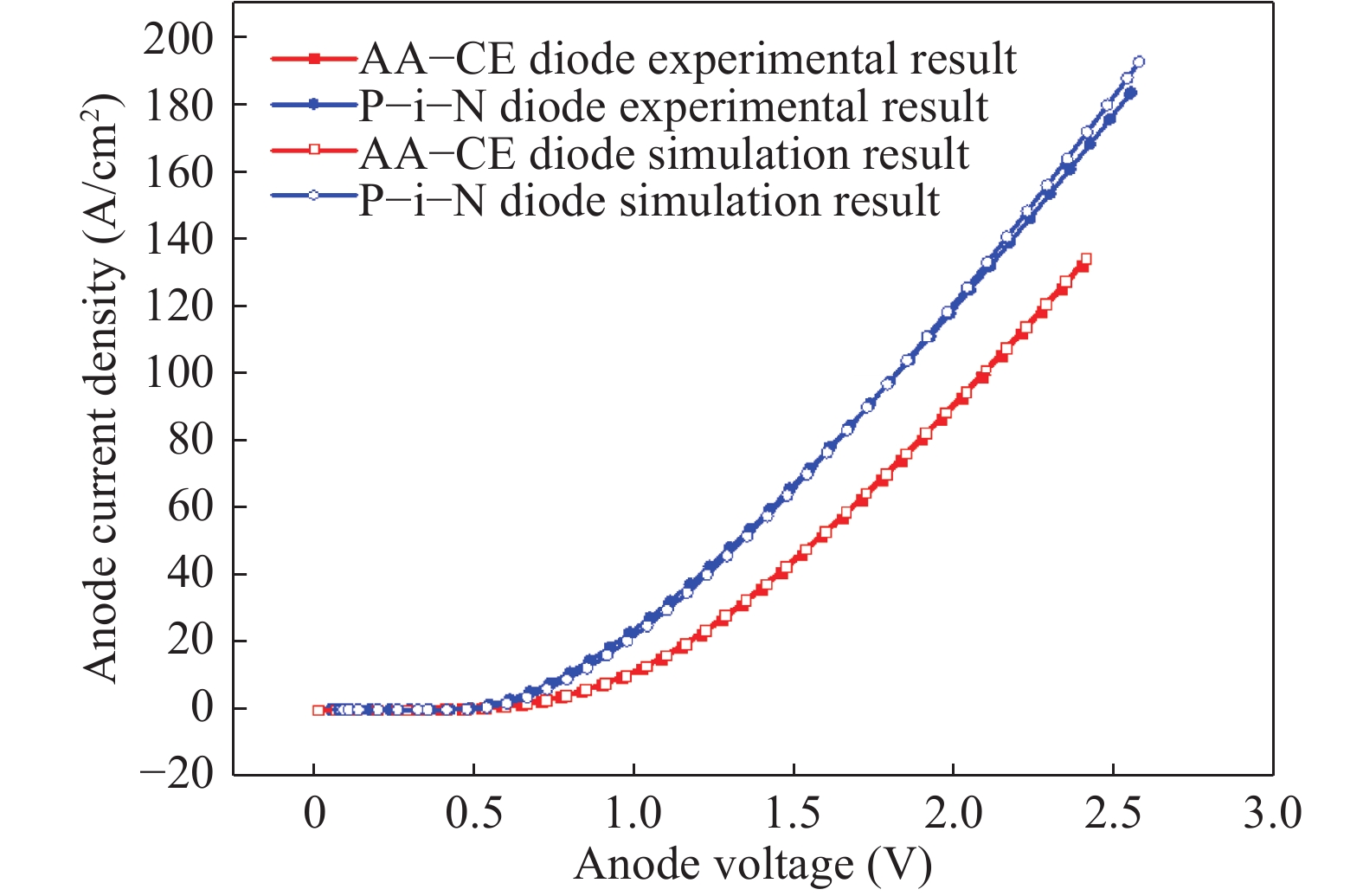
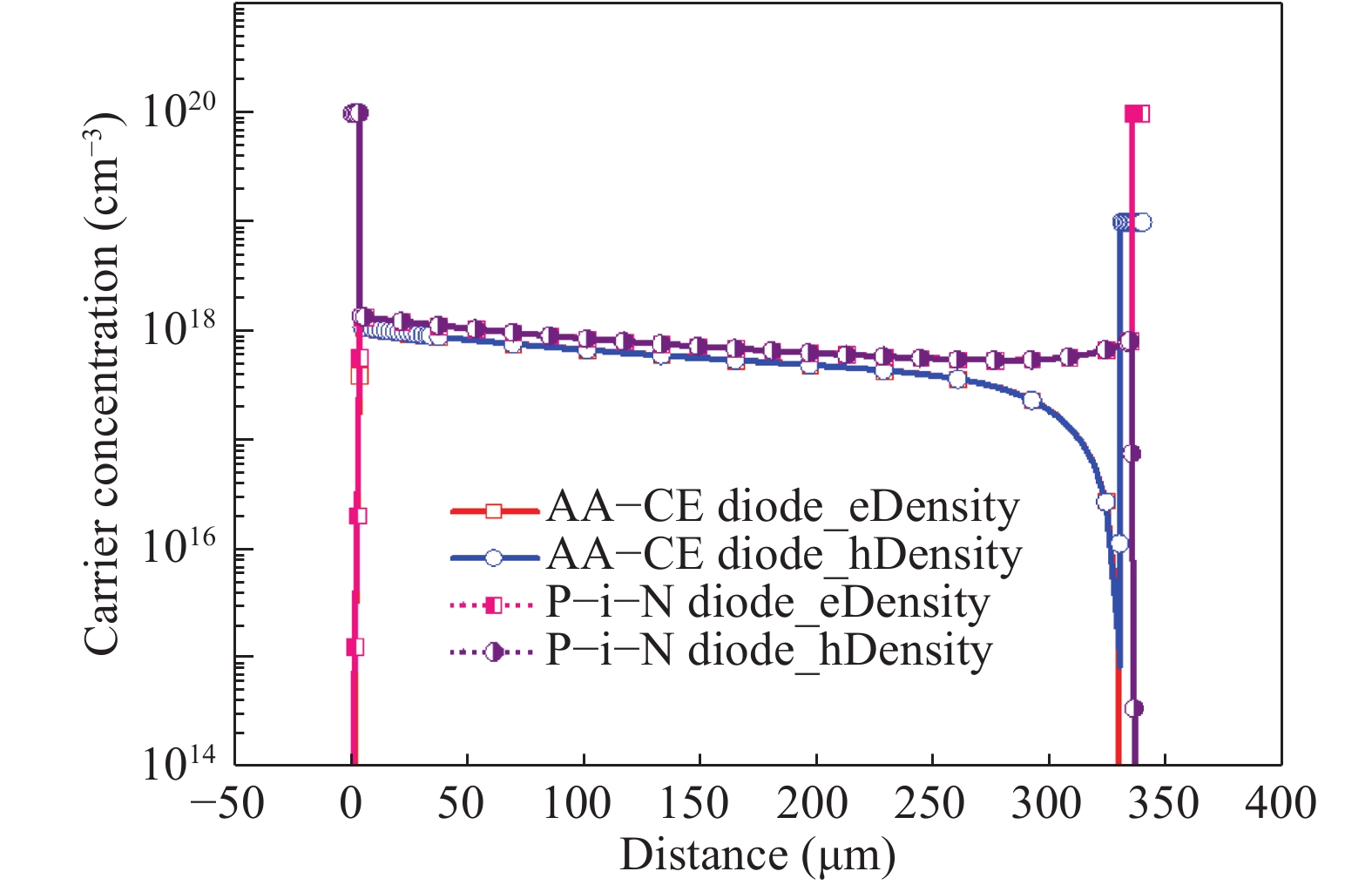
This paper presents an asymmetric anode structure and cathode extraction fast and soft recovery diode. The device anode is partial-heavily doped and partial-lightly doped. The P+ region is introduced into the cathode. Firstly, the characteristics of the diode are simulated and analyzed. Secondly, the diode was fabricated and its characteristics were tested. The experimental results are in good agreement with the simulation results. The results show that, compared with the P–i–N diode, although the forward conduction characteristic of the diode is declined, the reverse recovery peak current is reduced by 47%, the reverse recovery time is shortened by 20% and the softness factor is doubled. In addition, the breakdown voltage is increased by 10%.


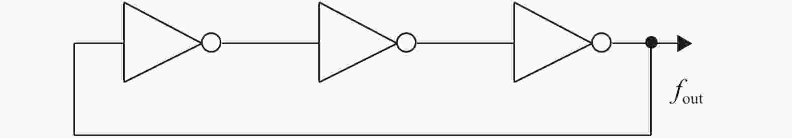
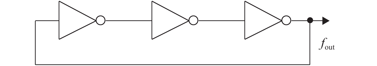
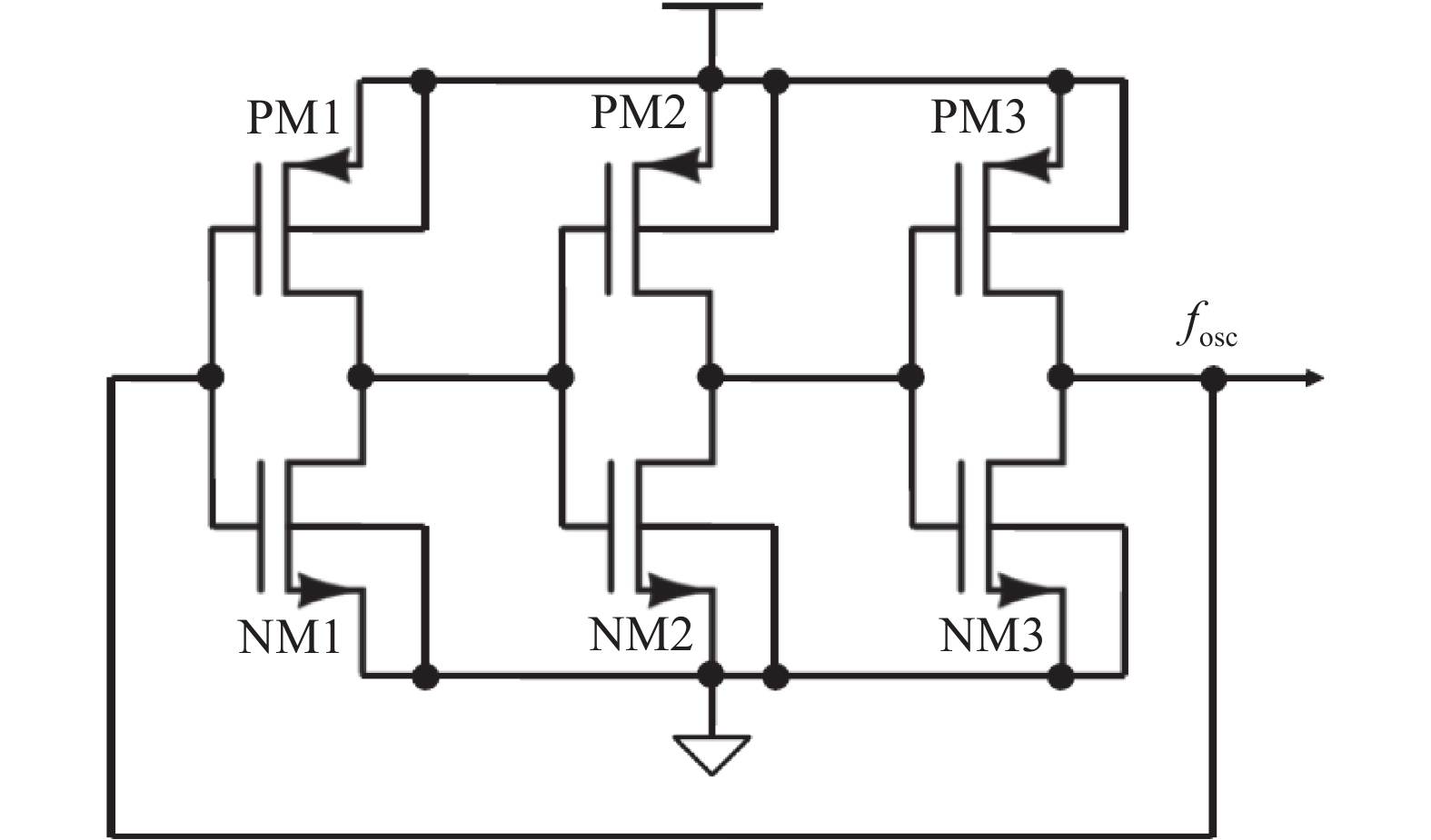
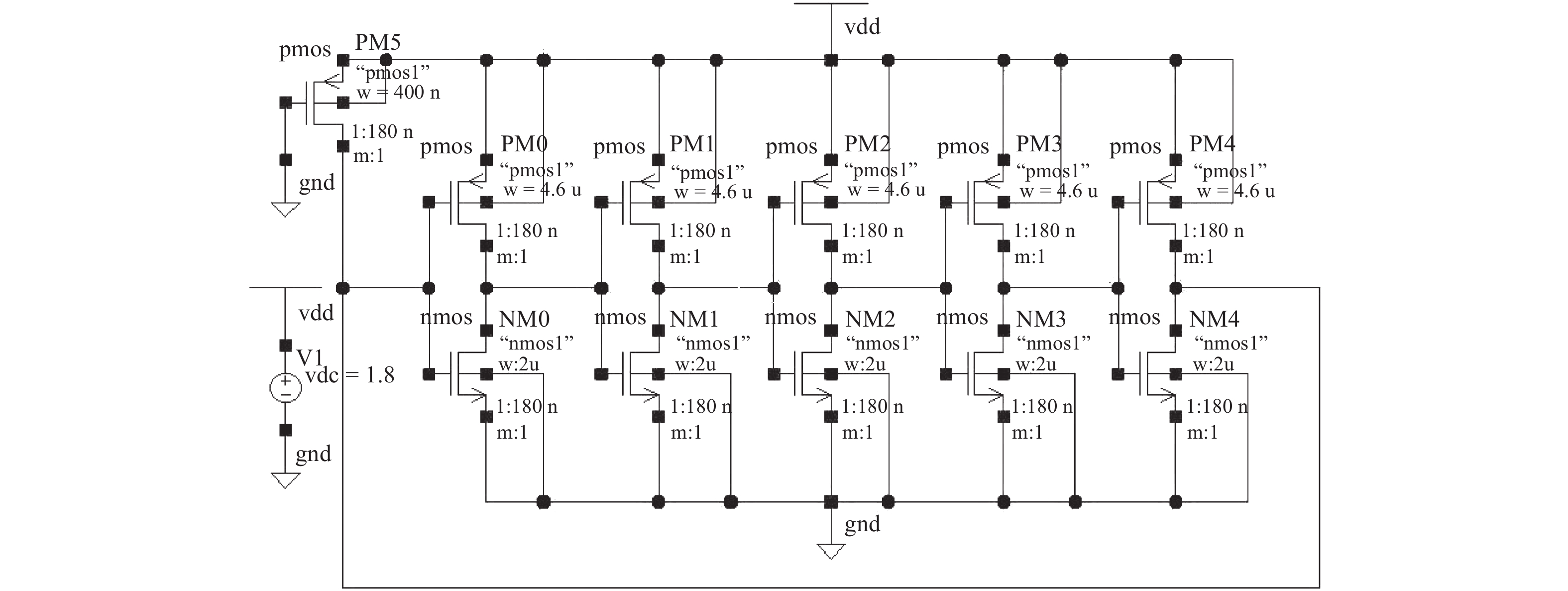
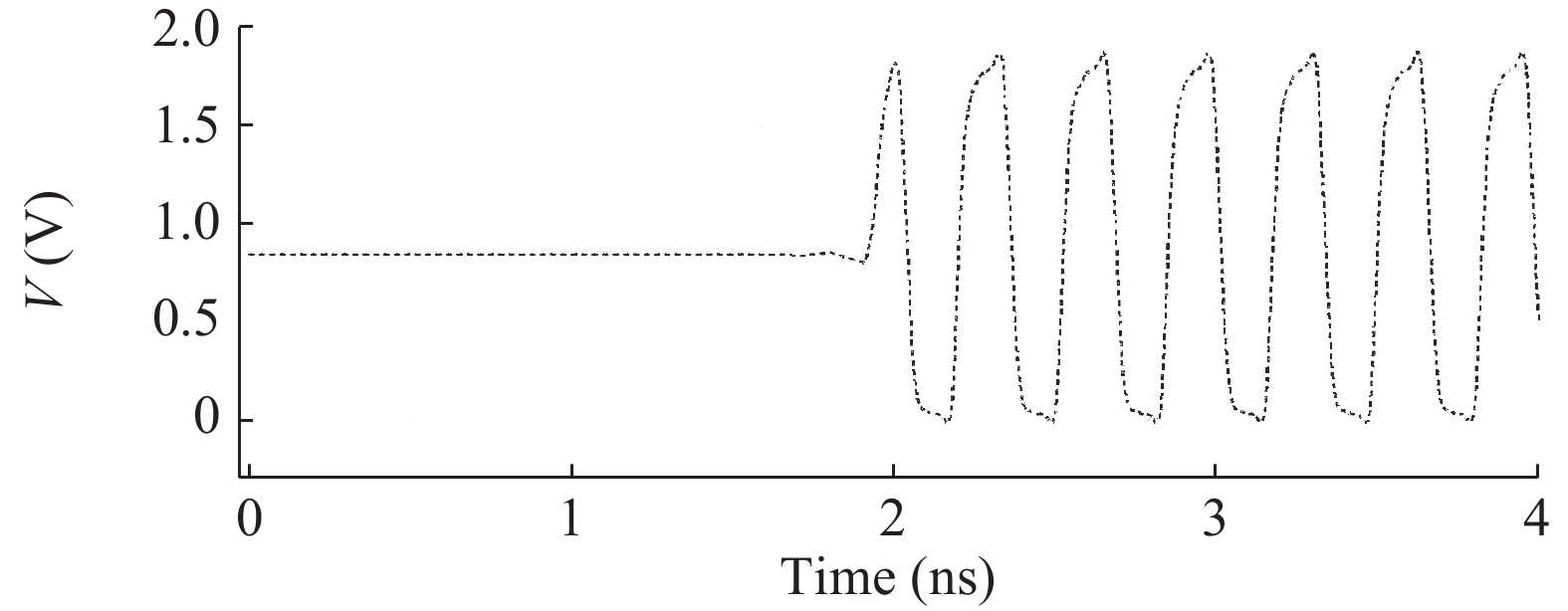
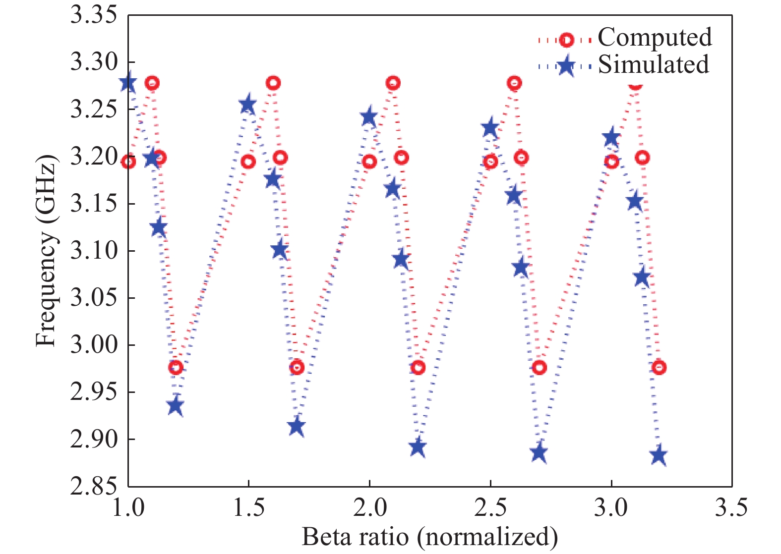
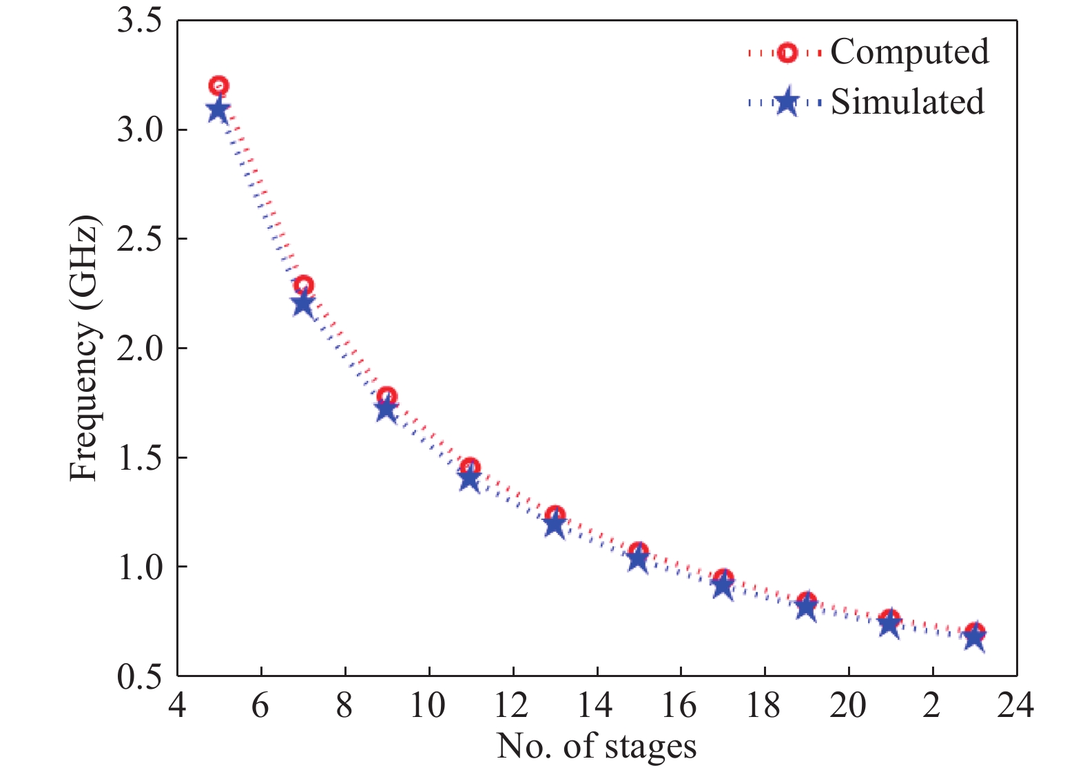
By utilizing the first order behavior of the device, an equation for the frequency of operation of the submicron CMOS ring oscillator is presented. A 5-stage ring oscillator is utilized as the initial design, with different Beta ratios, for the computation of the operating frequency. Later on, the circuit simulation is performed from 5-stage till 23-stage, with the range of oscillating frequency being 3.0817 and 0.6705 GHz respectively. It is noted that the output frequency is inversely proportional to the square of the device length, and when the value of Beta ratio is used as 2.3, a difference of 3.64% is observed on an average, in between the computed and the simulated values of frequency. As an outcome, the derived equation can be utilized, with the inclusion of an empirical constant in general, for arriving at the ring oscillator circuit’s output frequency.
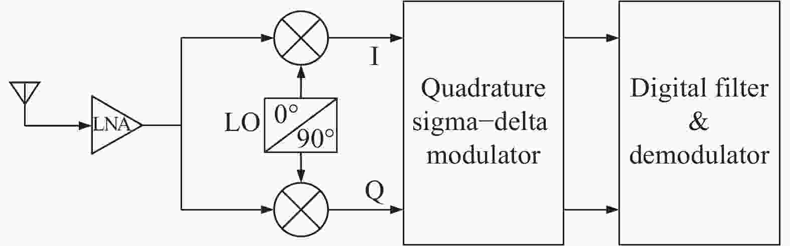
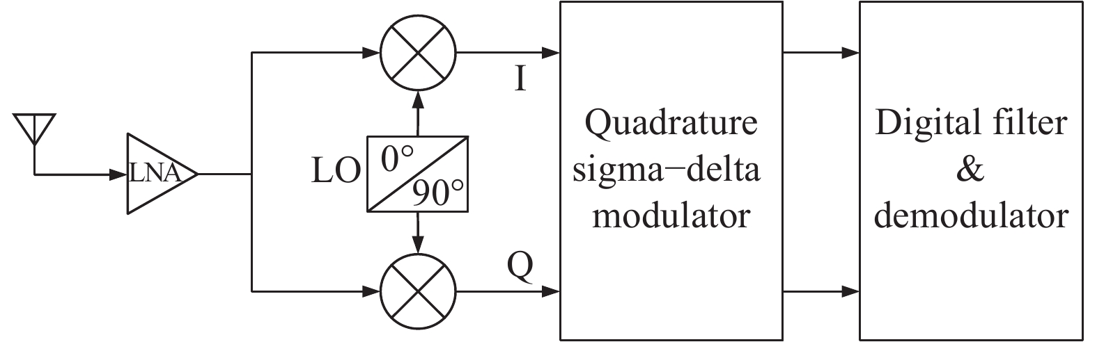
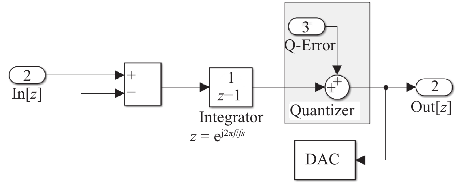
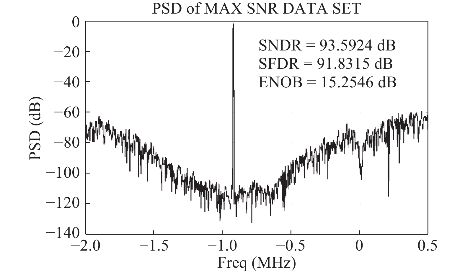
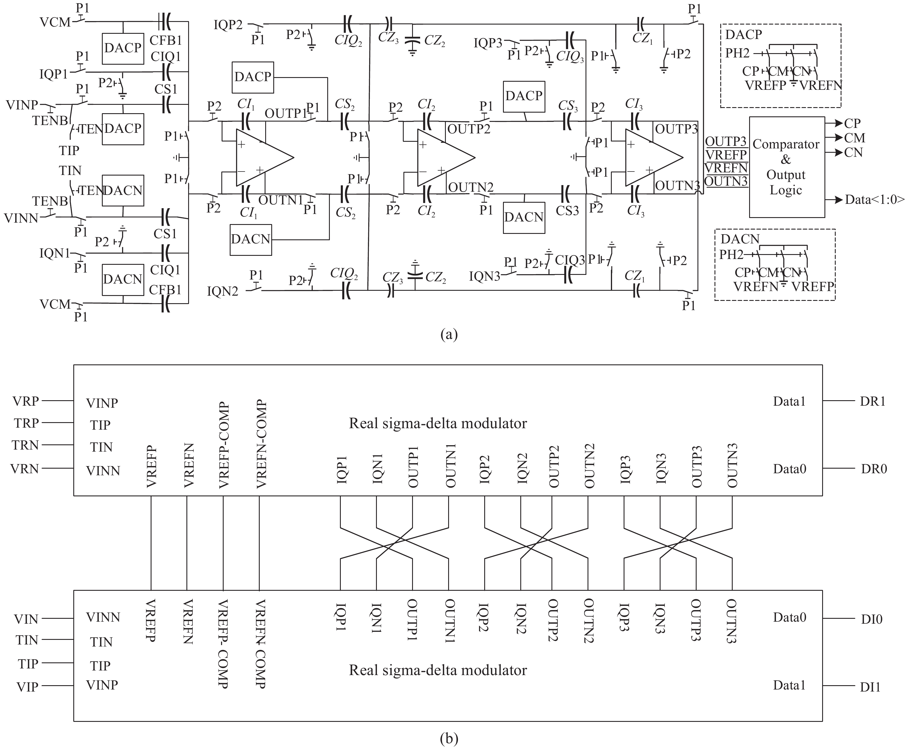
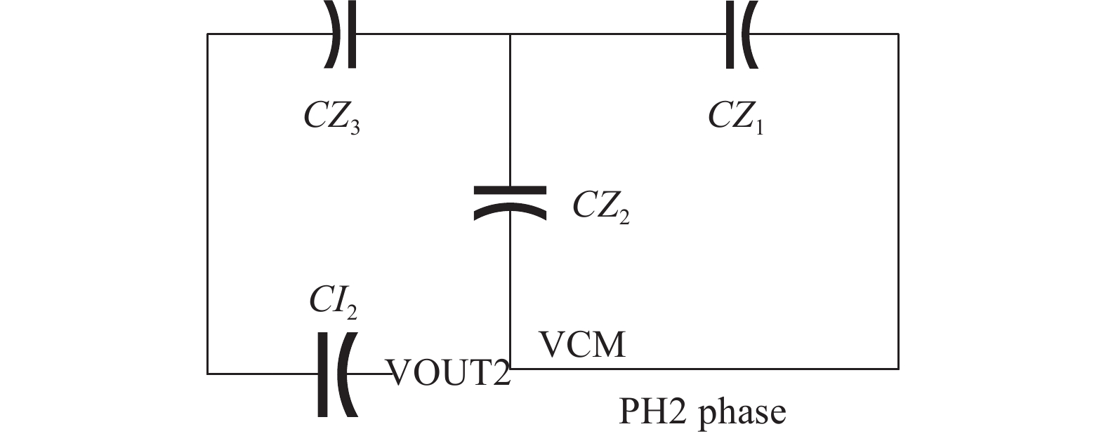
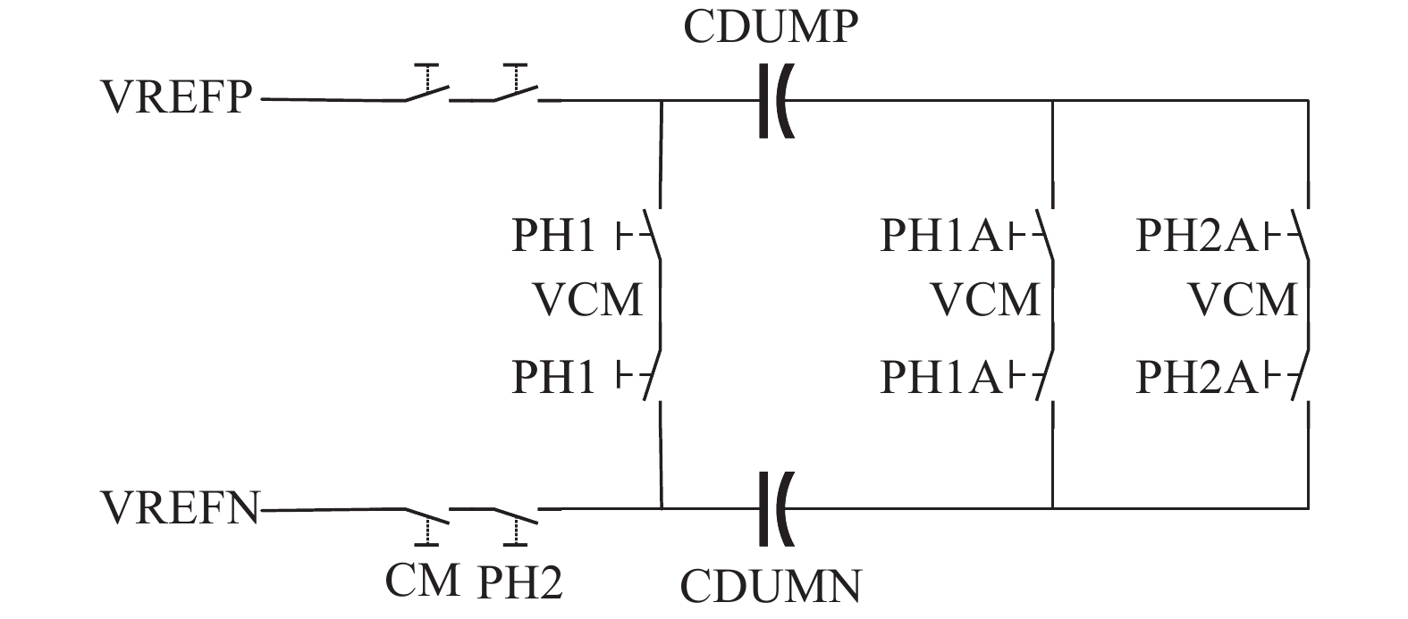
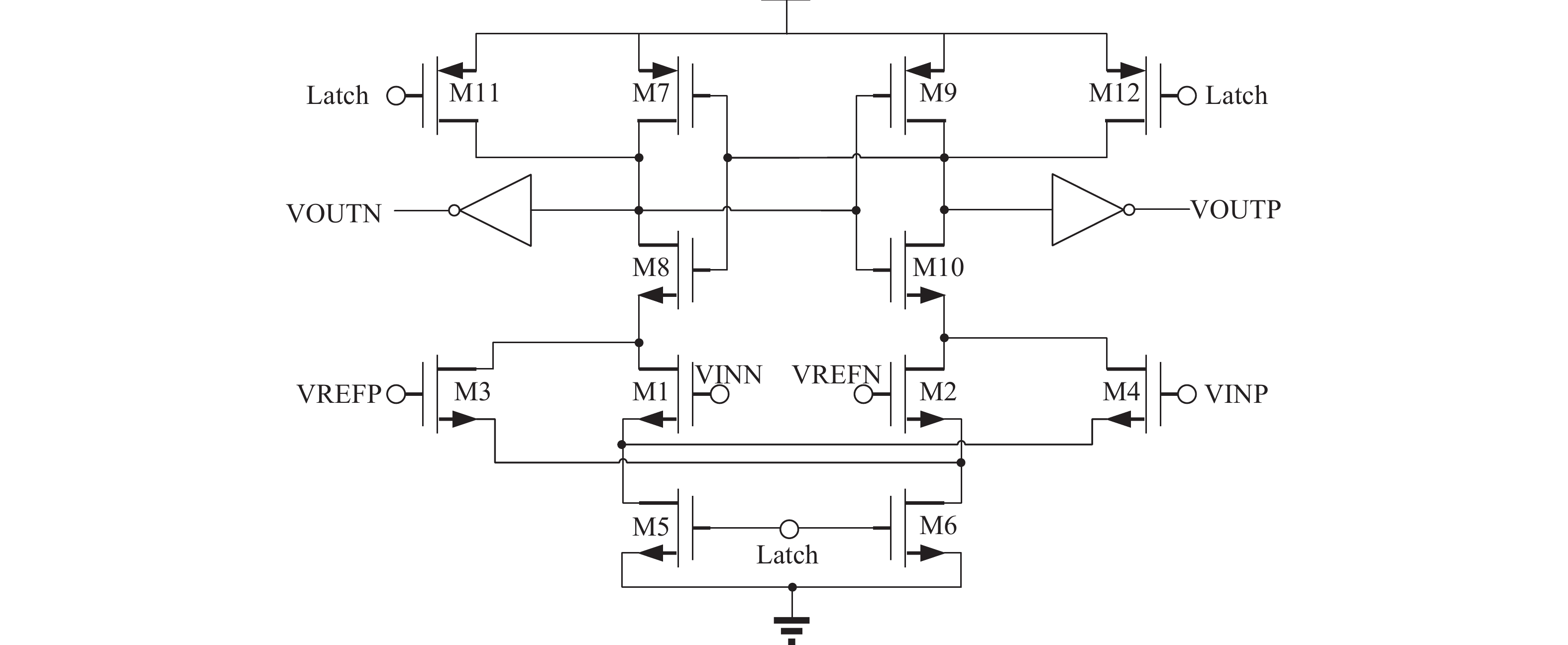
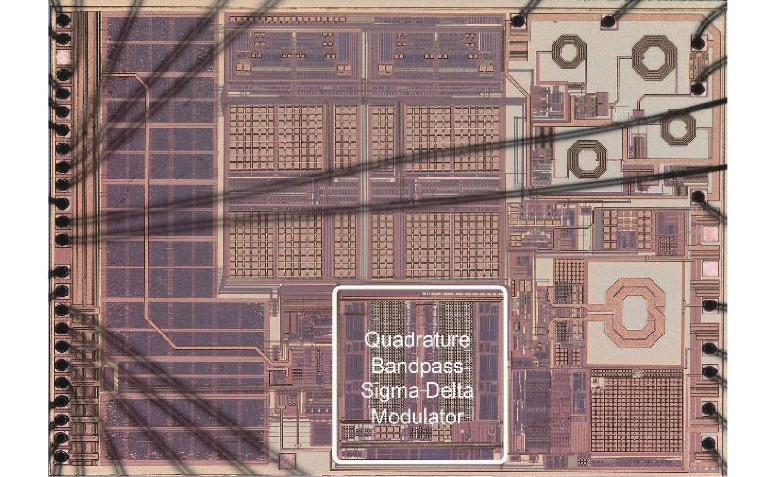
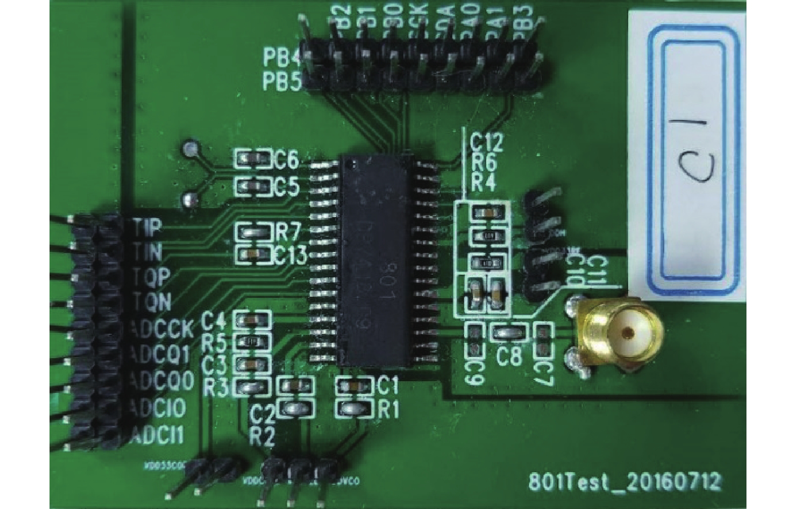
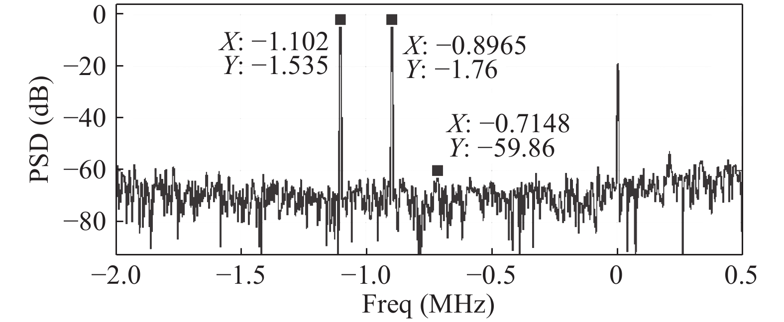
This paper presents the design and implementation of quadrature bandpass sigma–delta modulator. A pole movement method for transforming real sigma–delta modulator to a quadrature one is proposed by detailed study of the relationship of noise-shaping center frequency and integrator pole position in sigma–delta modulator. The proposed modulator uses sampling capacitor sharing switched capacitor integrator, and achieves a very small feedback coefficient by a series capacitor network, and those two techniques can dramatically reduce capacitor area. Quantizer output-dependent dummy capacitor load for reference voltage buffer can compensate signal-dependent noise that is caused by load variation. This paper designs a quadrature bandpass Sigma-Delta modulator for 2.4 GHz low IF receivers that achieve 69 dB SNDR at 1 MHz BW and −1 MHz IF with 48 MHz clock. The chip is fabricated with SMIC 0.18 μm CMOS technology, it achieves a total power current of 2.1 mA, and the chip area is 0.48 mm2.


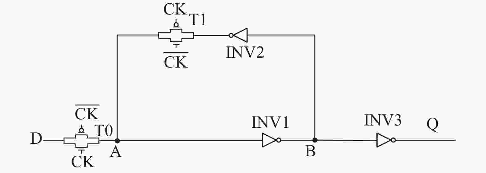
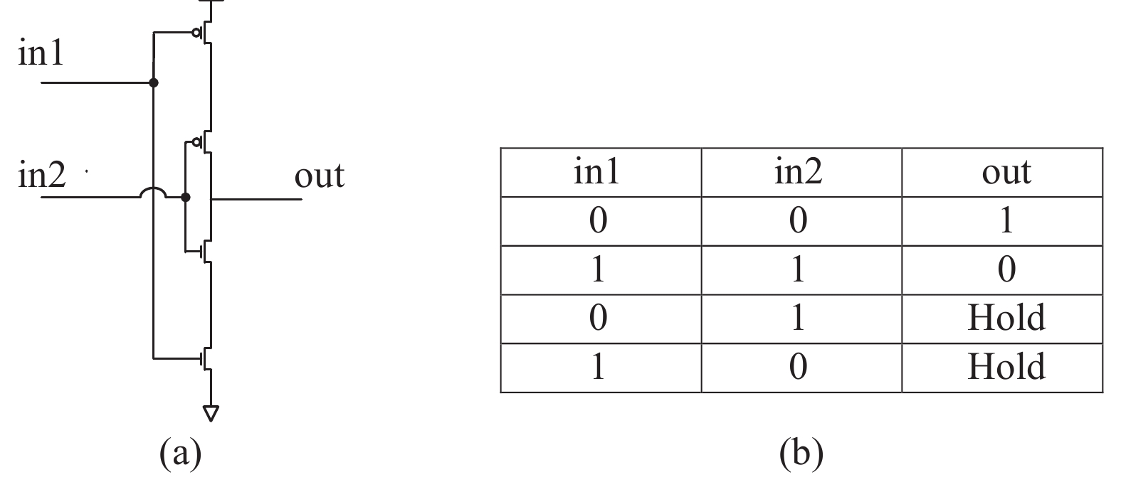
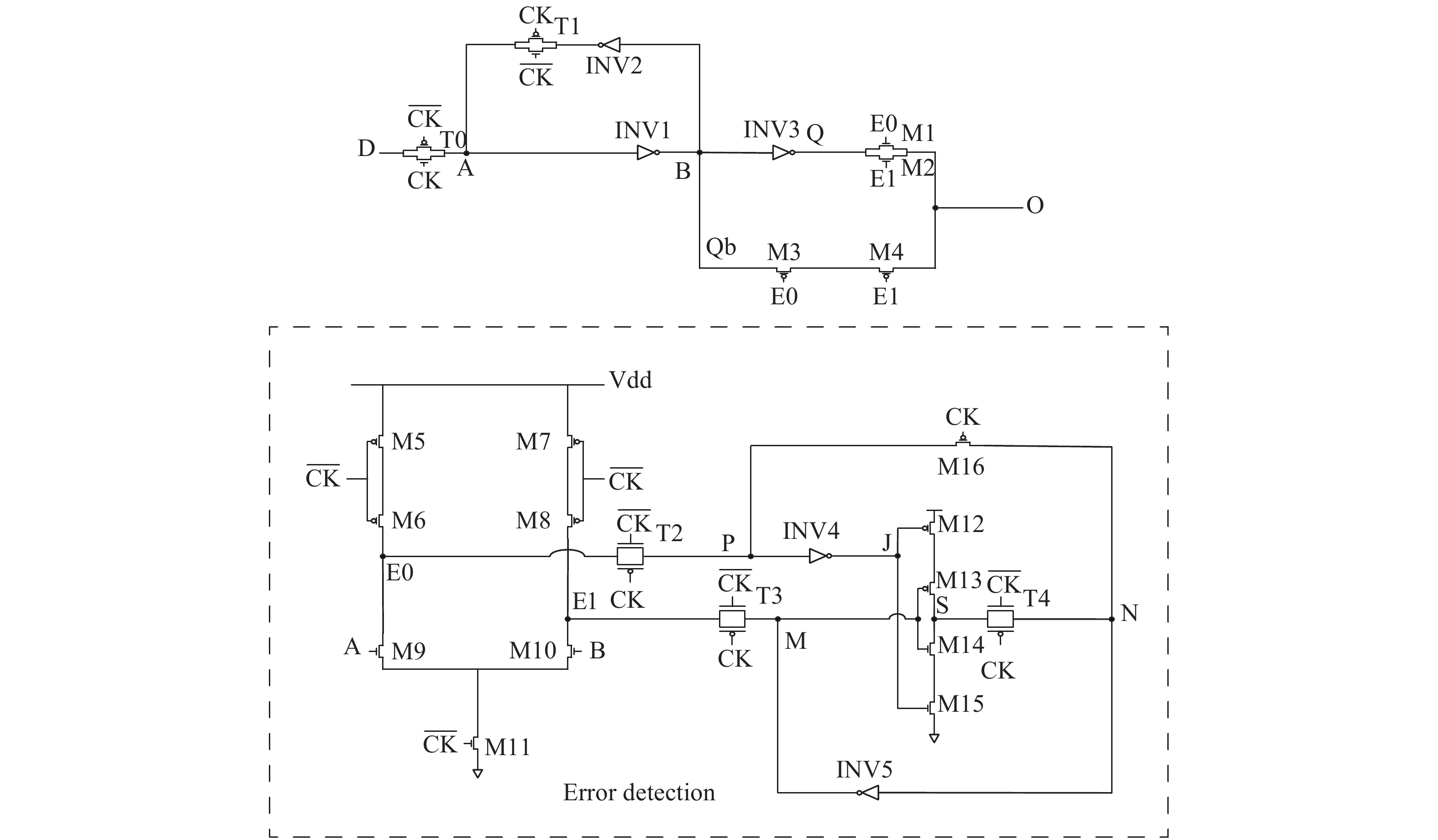
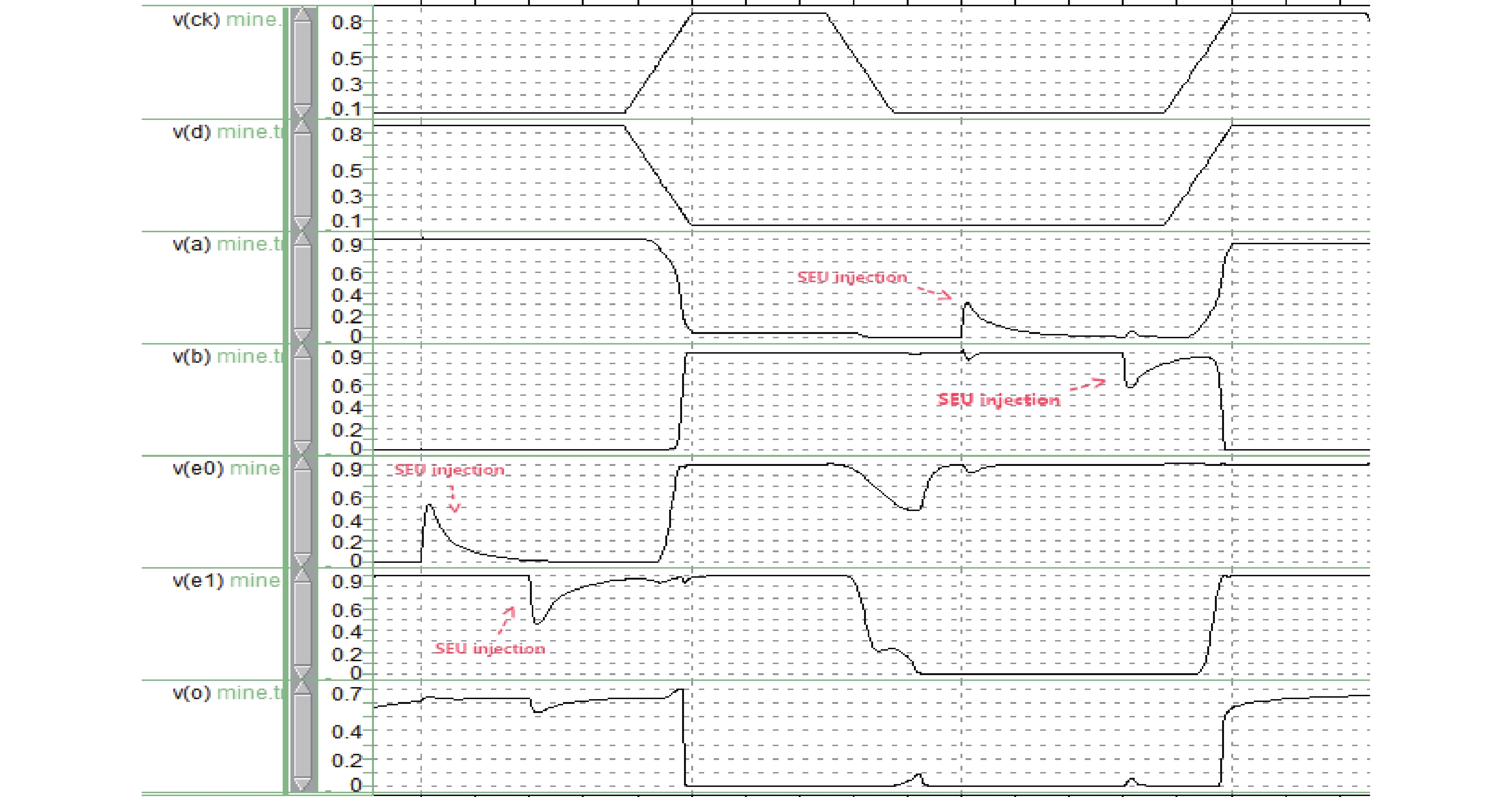
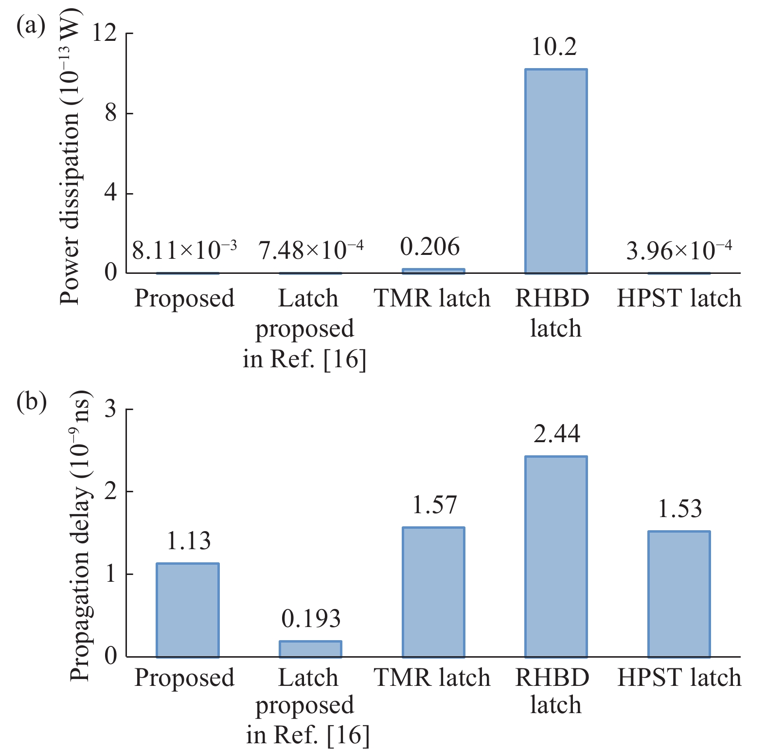
This paper proposes a latch that can mitigate SEUs via an error detection circuit. The error detection circuit is hardened by a C-element and a stacked PMOS. In the hold state, a particle strikes the latch or the error detection circuit may cause a fault logic state of the circuit. The error detection circuit can detect the upset node in the latch and the fault output will be corrected. The upset node in the error detection circuit can be corrected by the C-element. The power dissipation and propagation delay of the proposed latch are analyzed by HSPICE simulations. The proposed latch consumes about 77.5% less energy and 33.1% less propagation delay than the triple modular redundancy (TMR) latch. Simulation results demonstrate that the proposed latch can mitigate SEU effectively.