J. Semicond.
2018, 39(6): 061001
doi: 10.1088/1674-4926/39/6/061001
Xiaoxin Wang, Jifeng Liu. Emerging technologies in Si active photonics[J]. Journal of Semiconductors, 2018, 39(6): 061001. doi: 10.1088/1674-4926/39/6/061001.
X X Wang, J F Liu. Emerging technologies in Si active photonics[J]. J. Semicond., 2018, 39(6): 061001. doi: 10.1088/1674-4926/39/6/061001.Export: BibTex EndNote
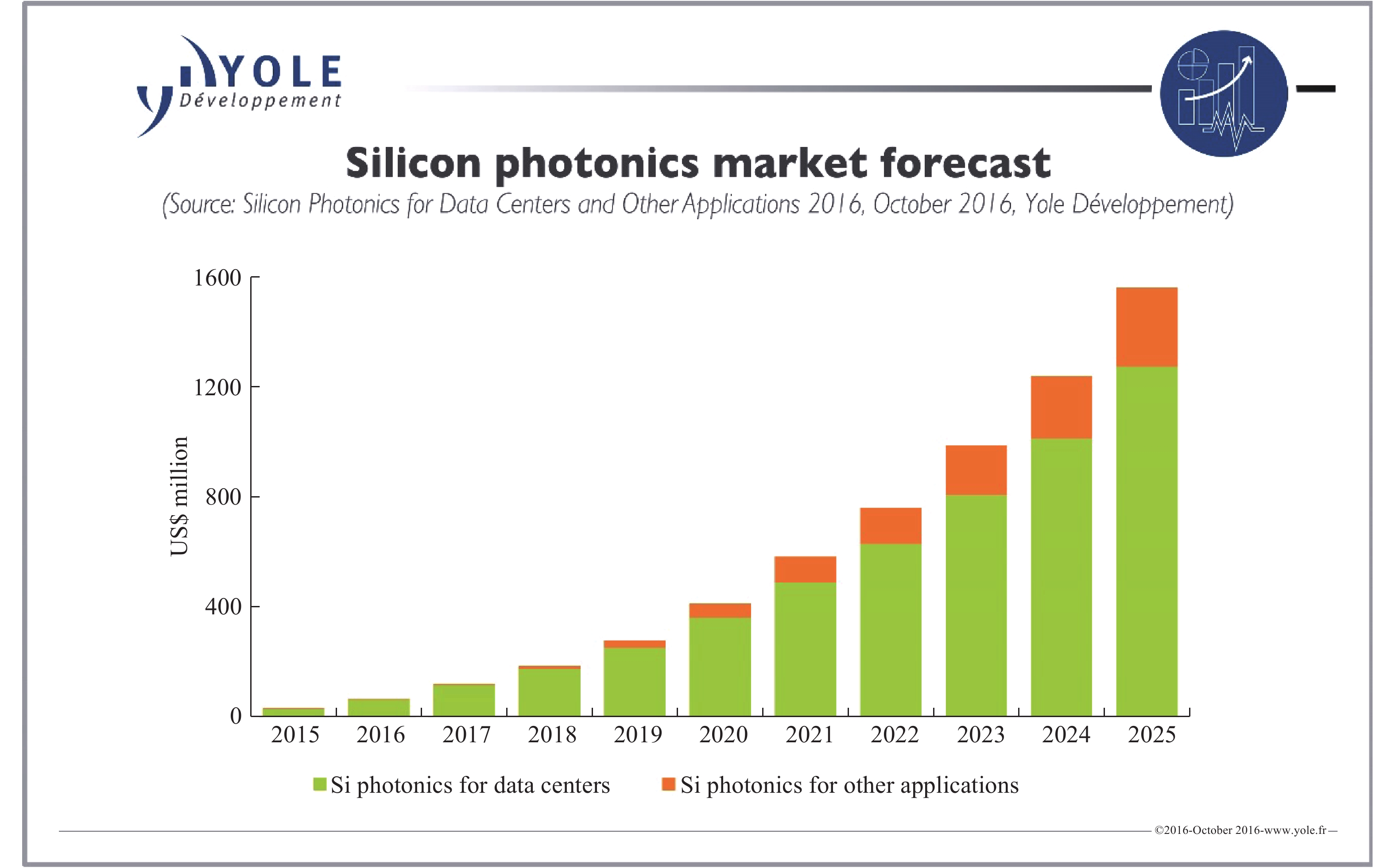
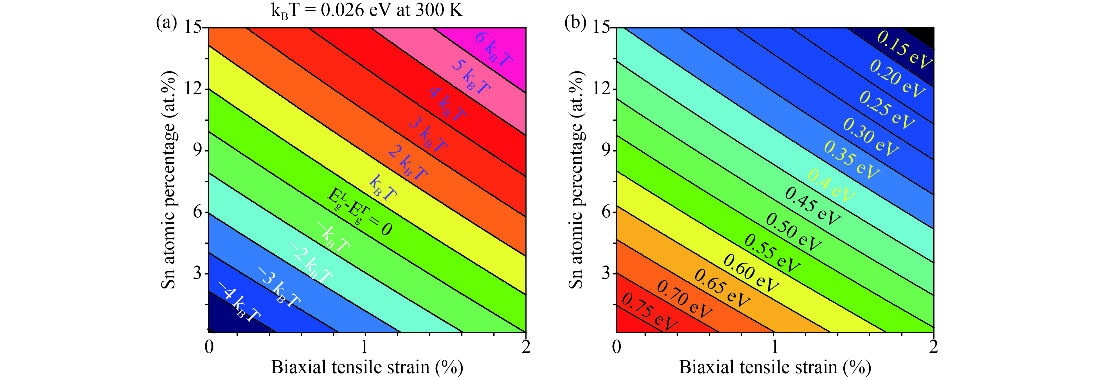
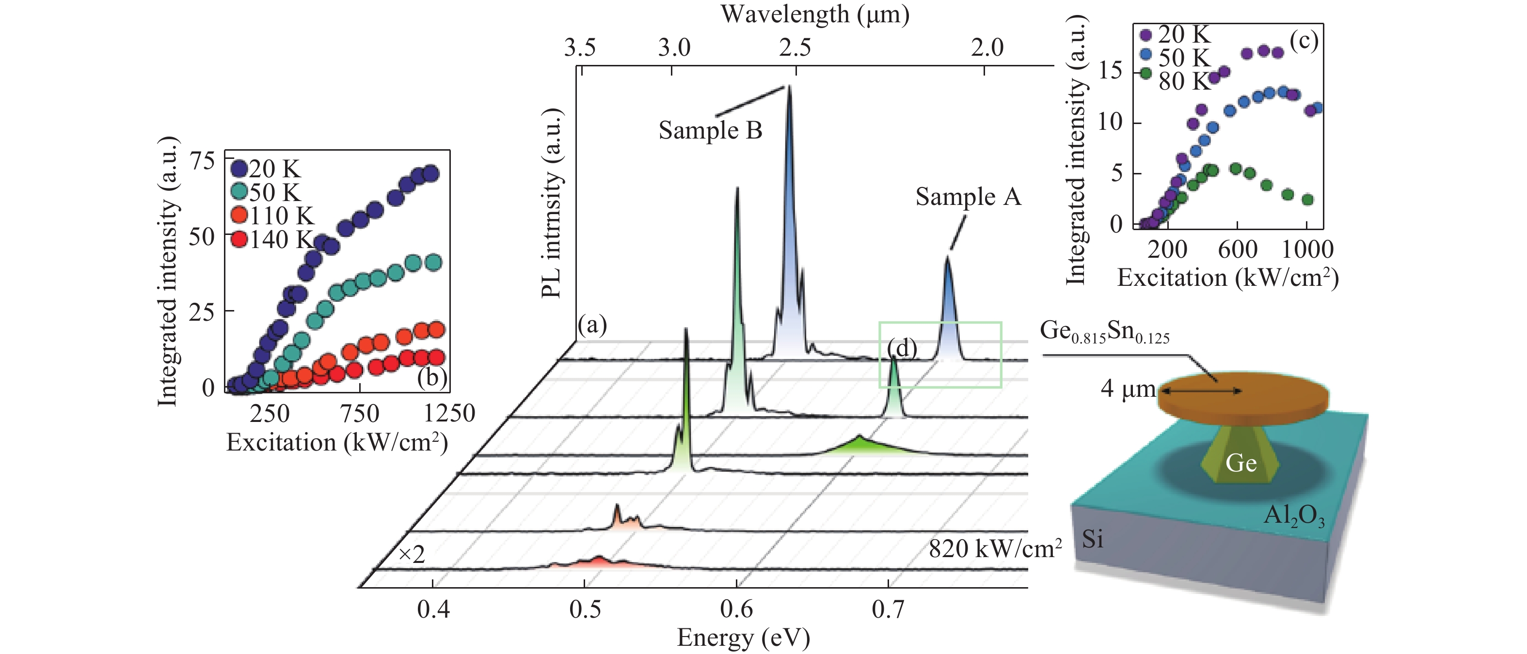
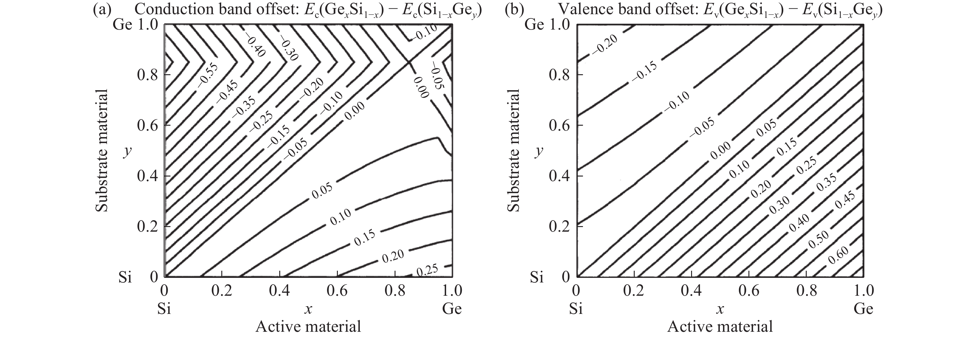
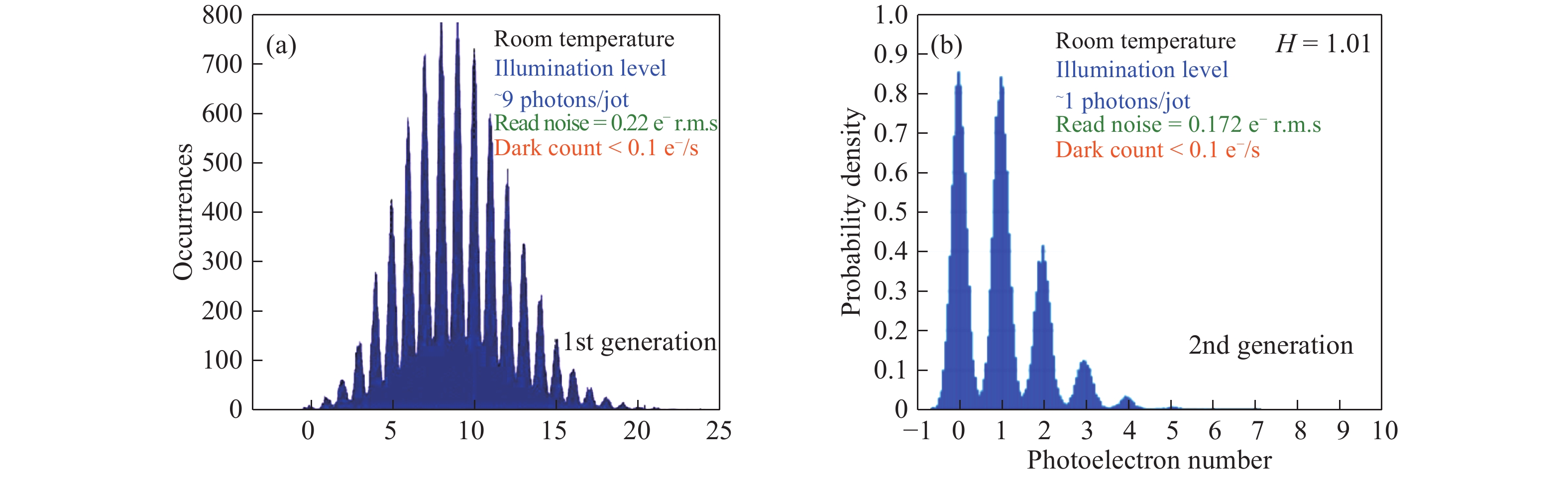
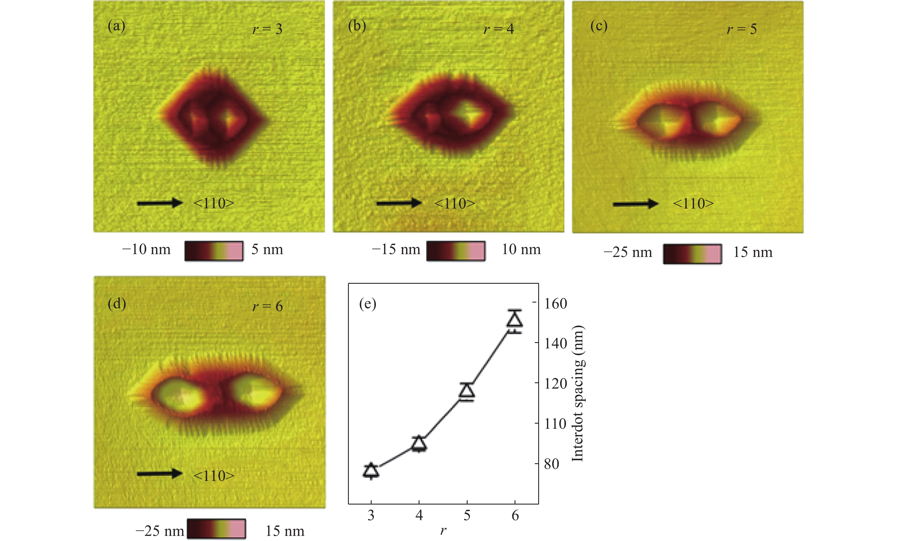
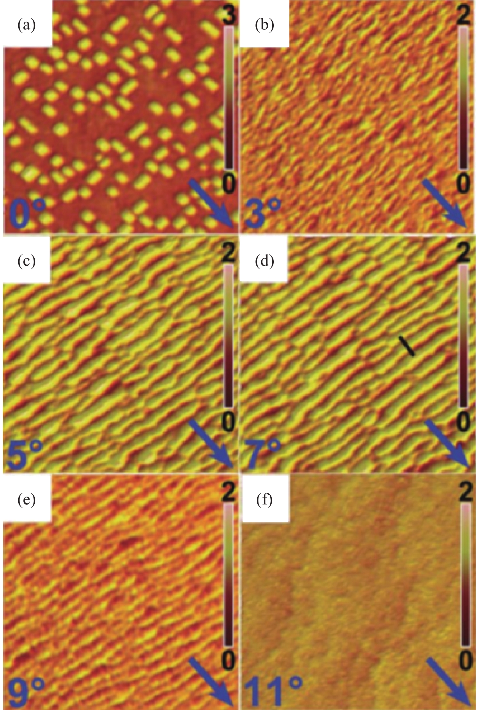
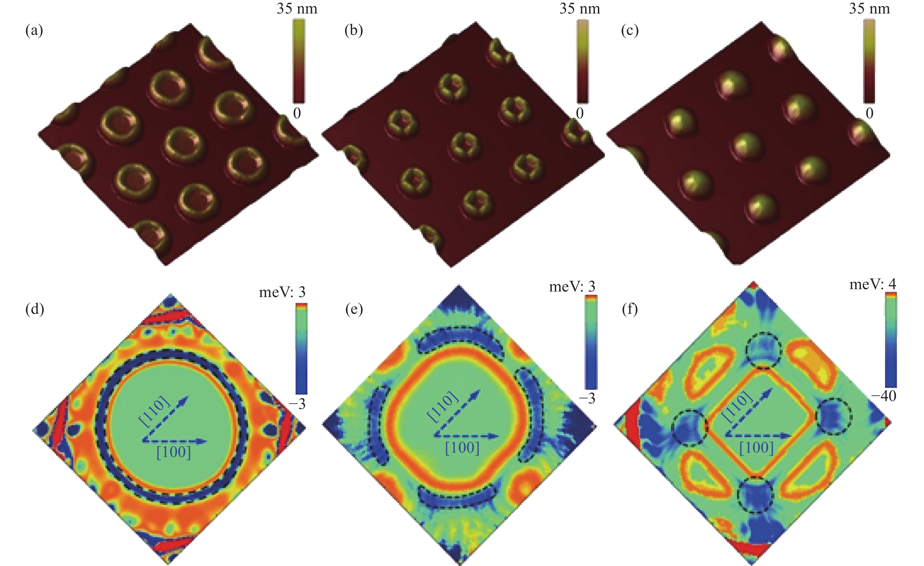
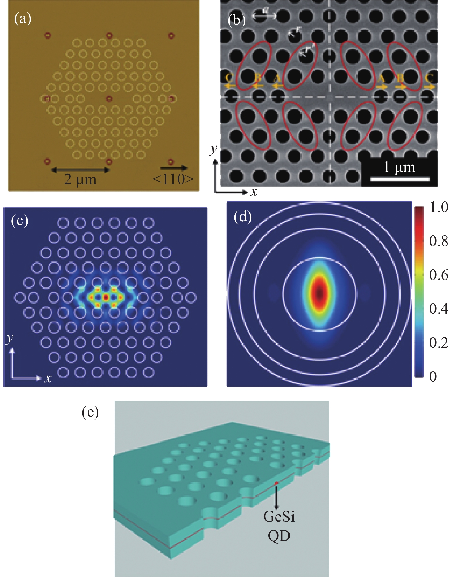
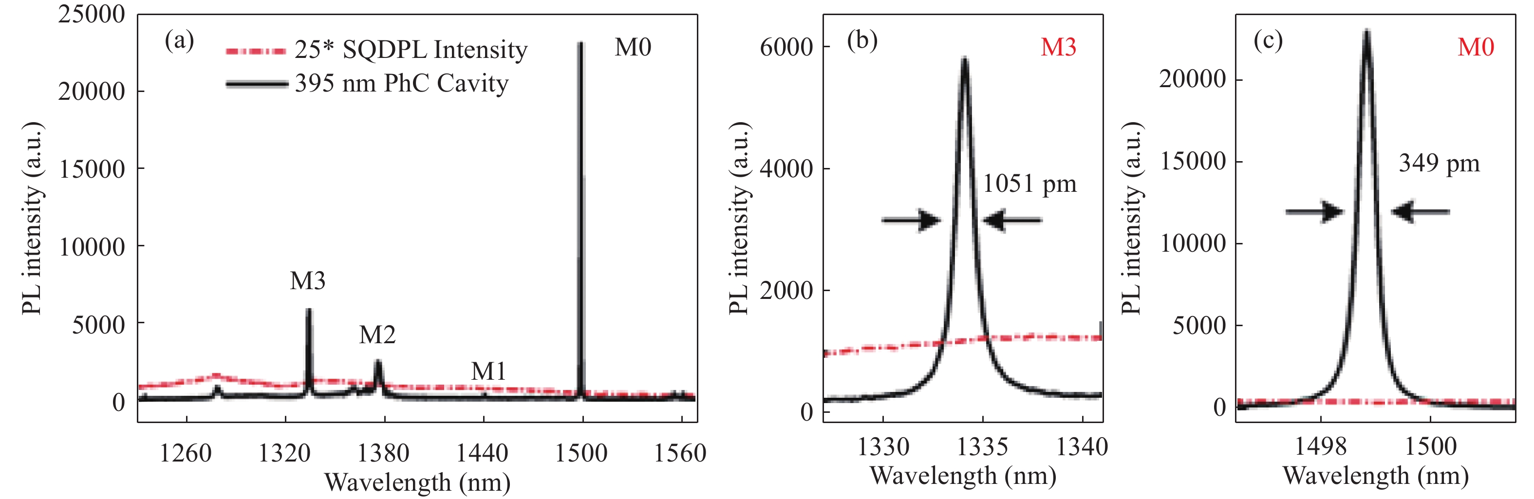
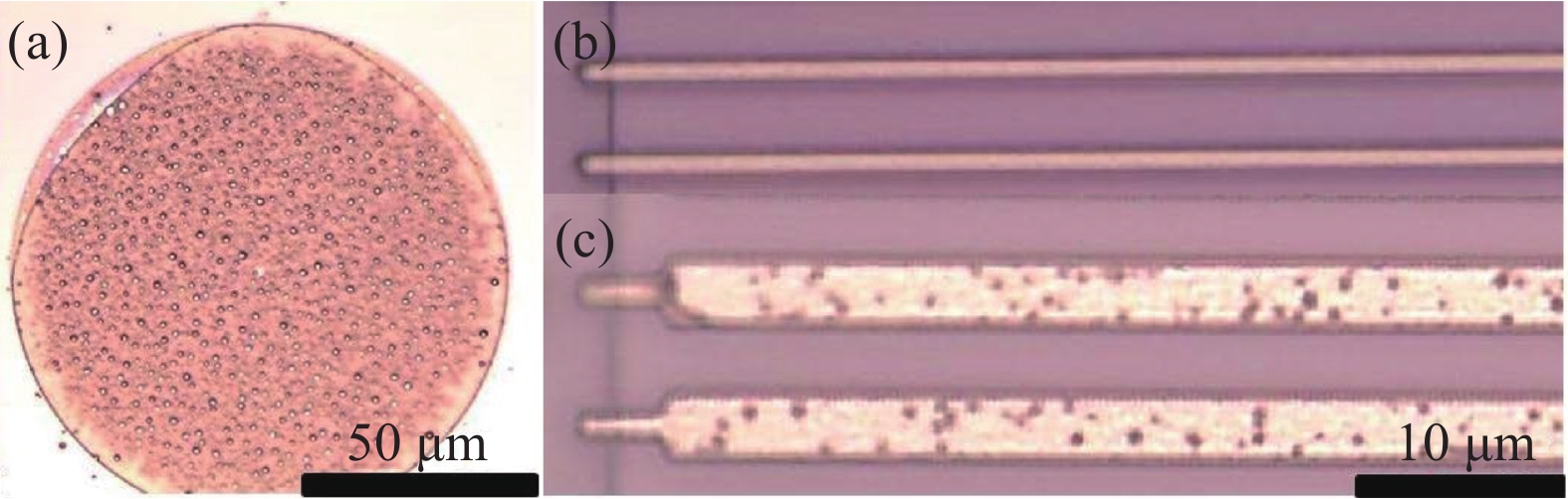
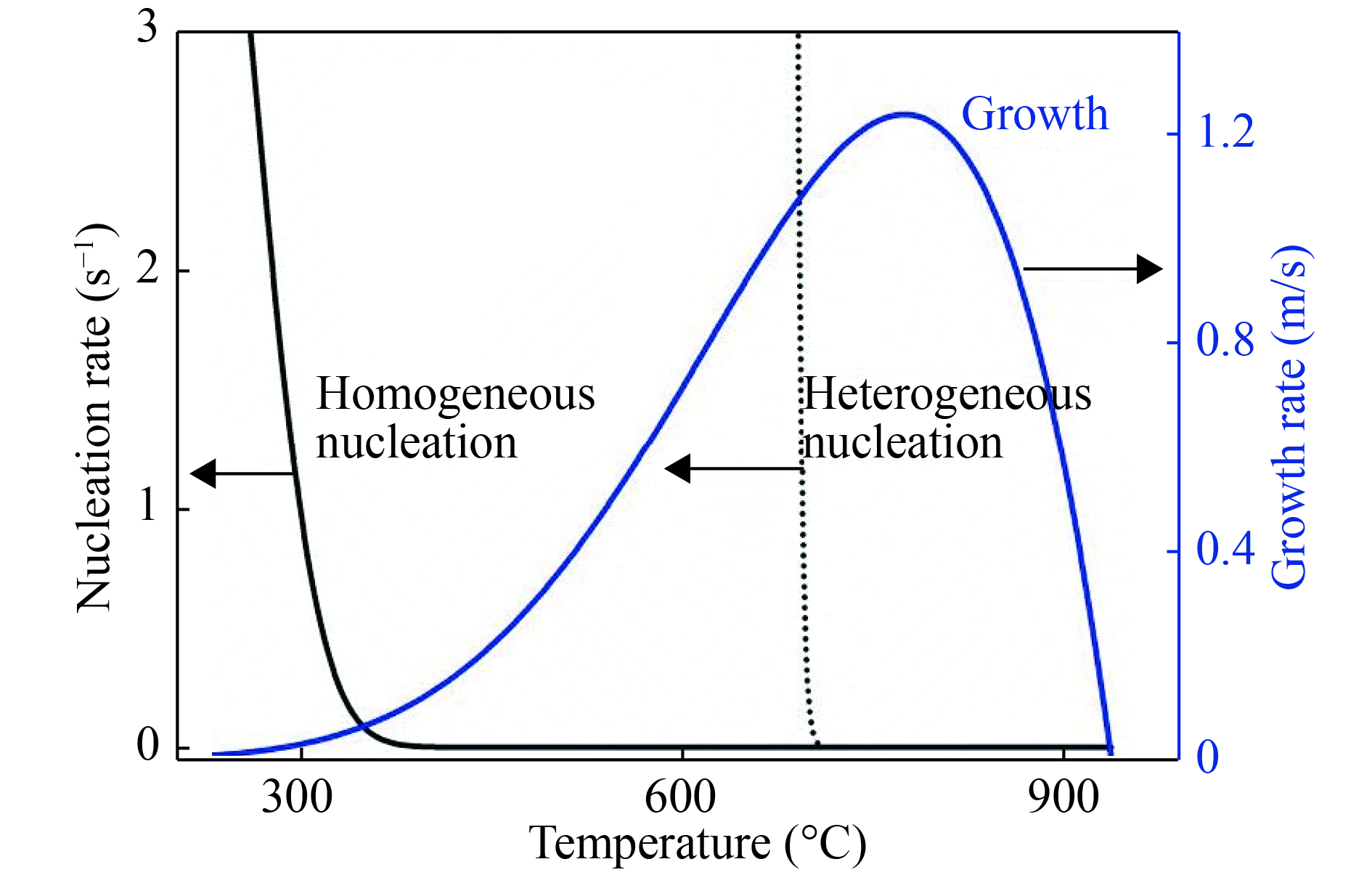
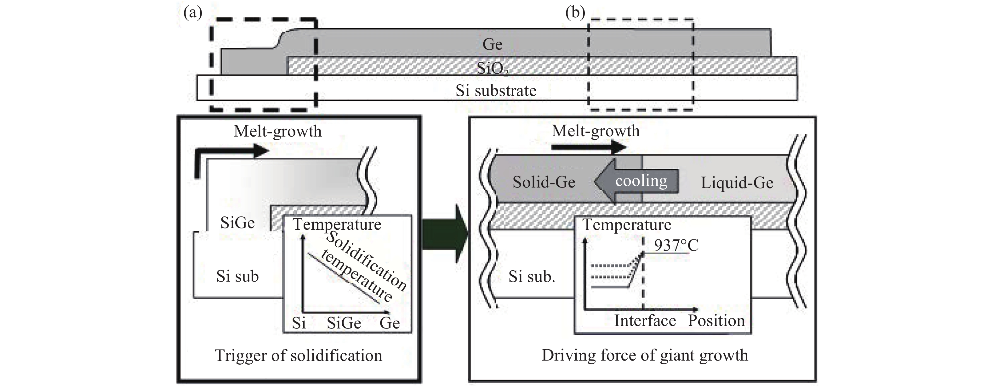
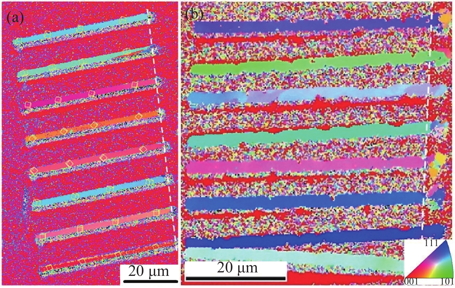
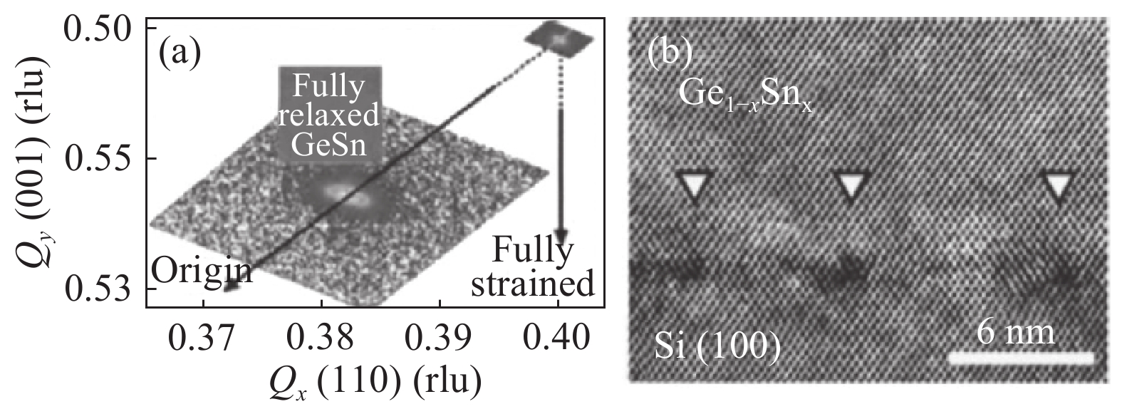
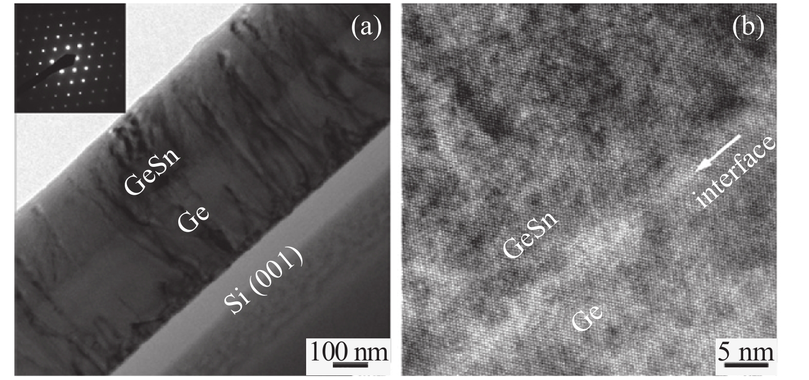
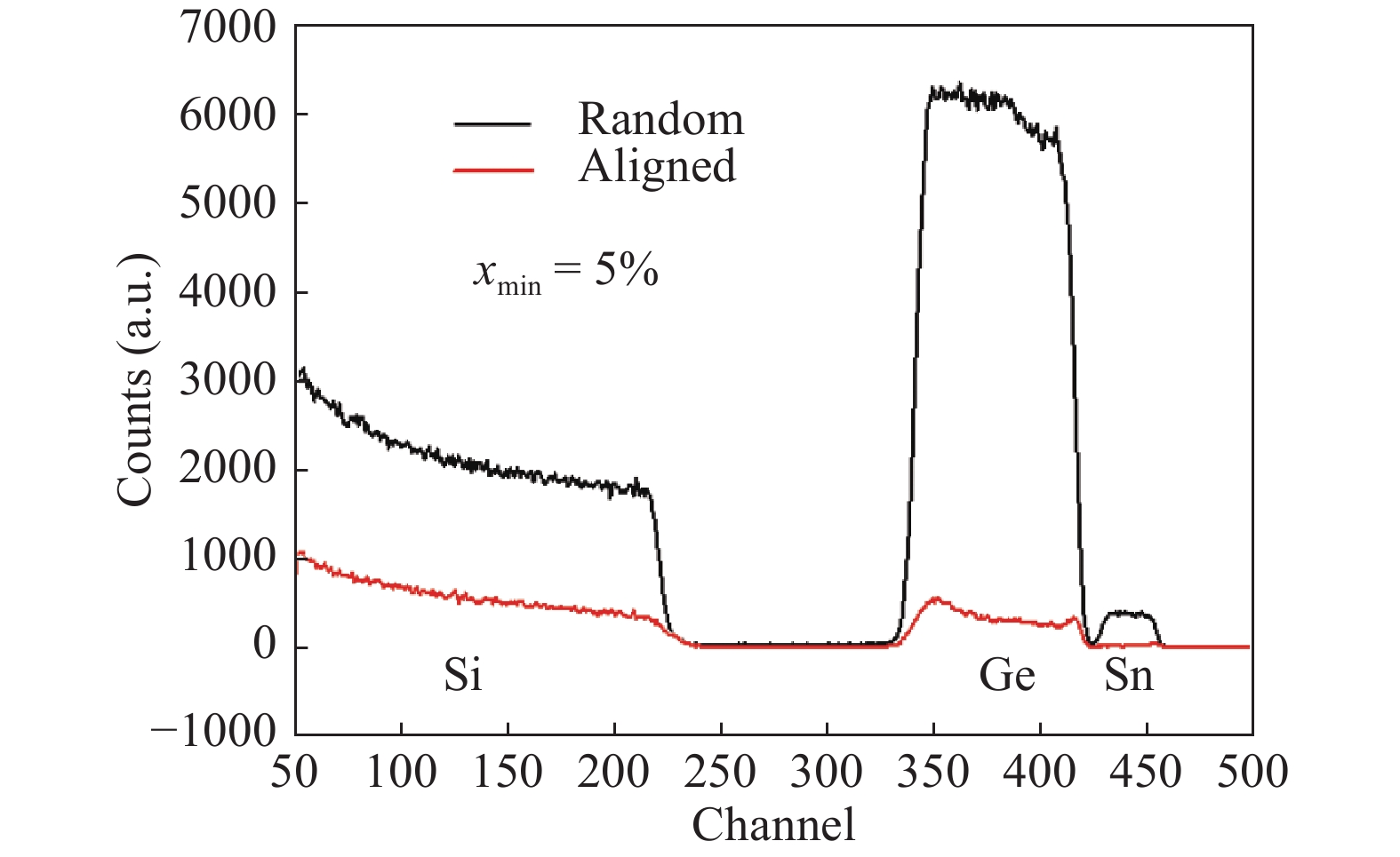
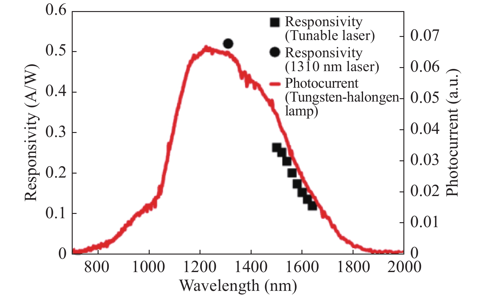
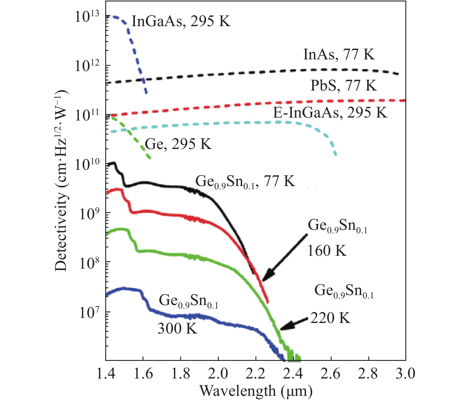
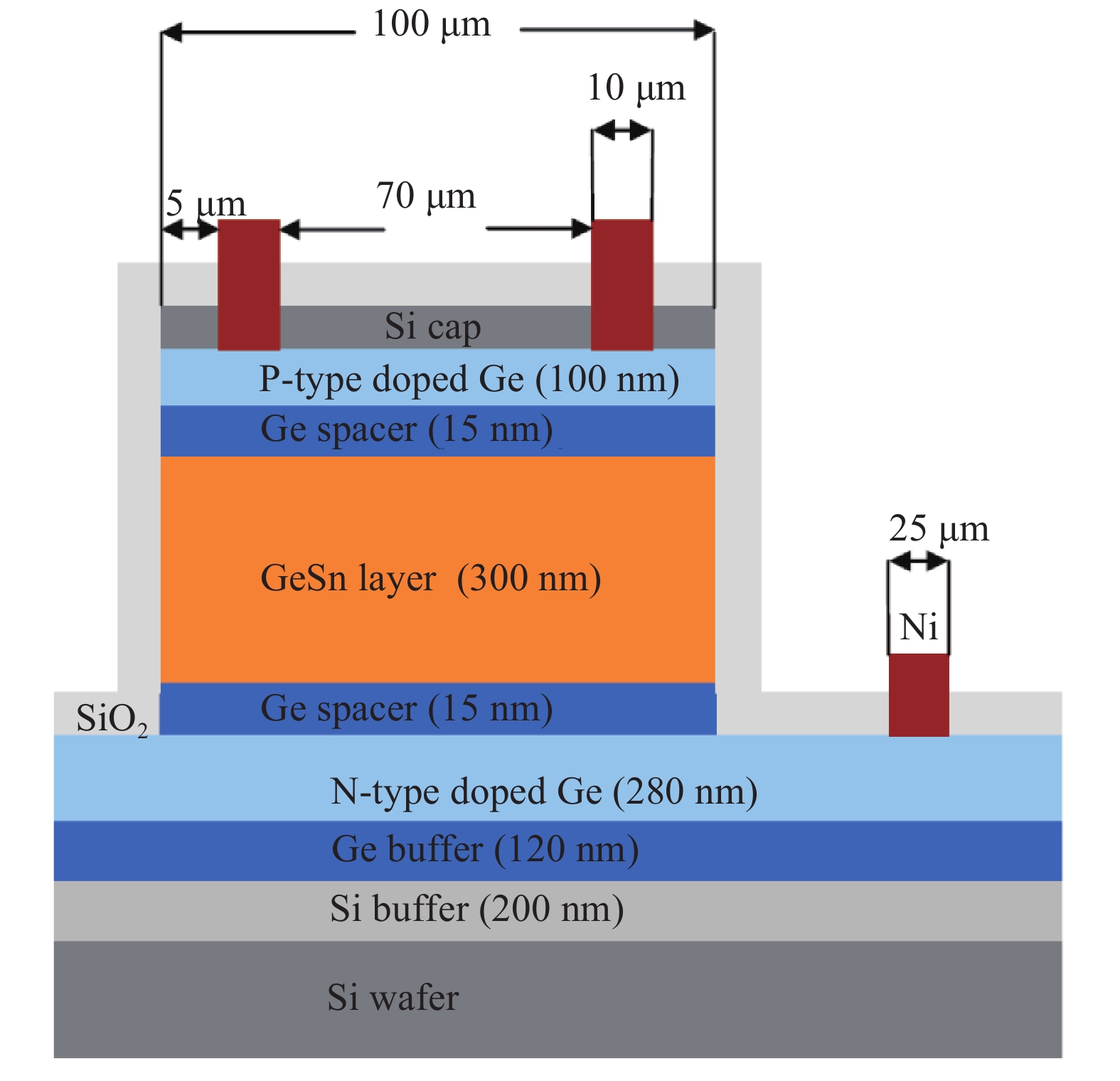
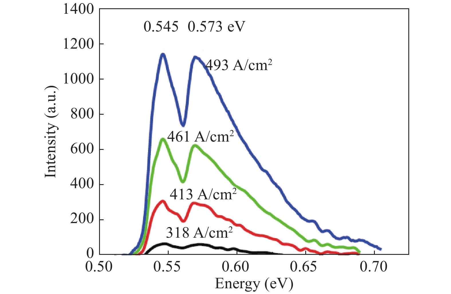
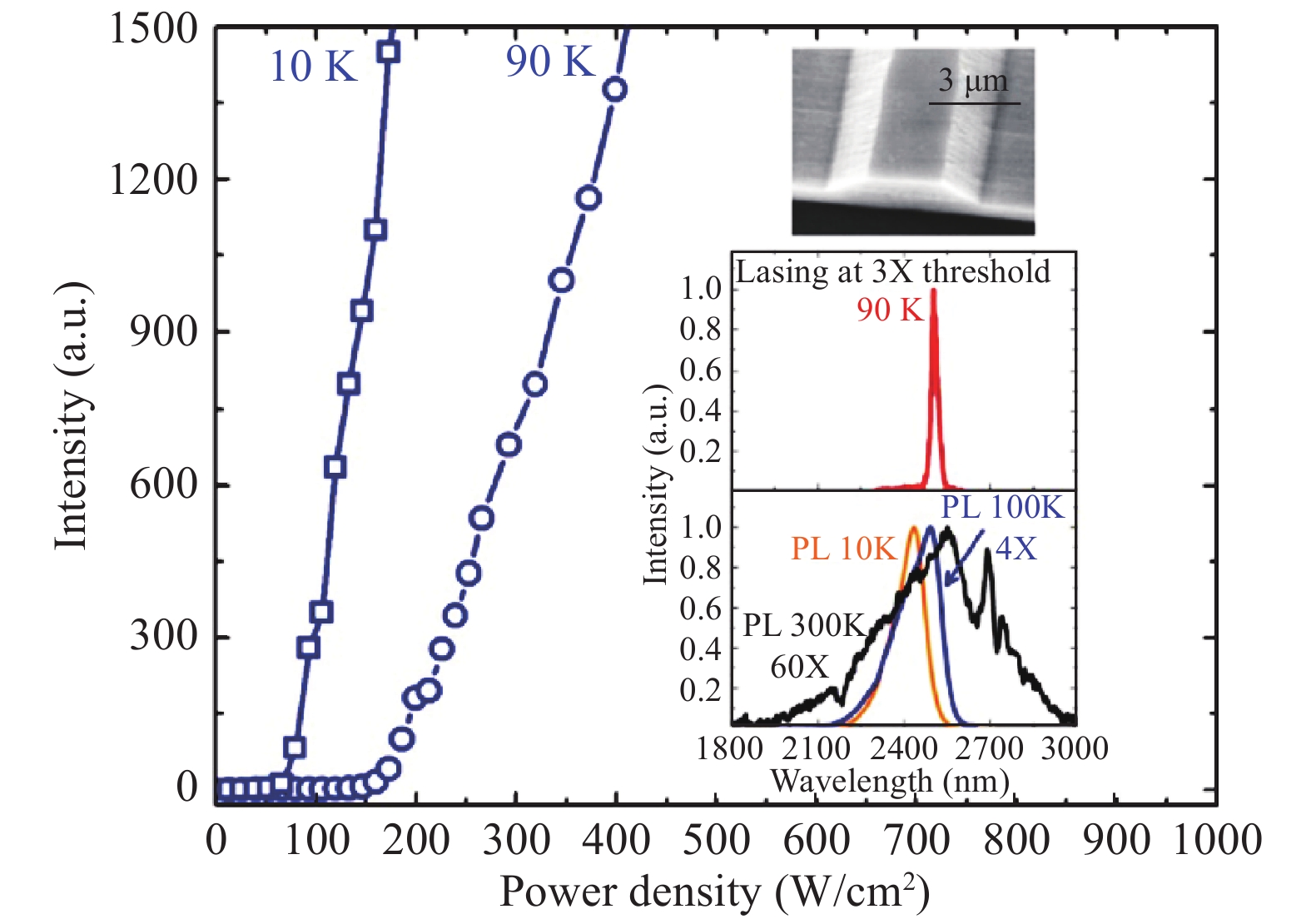
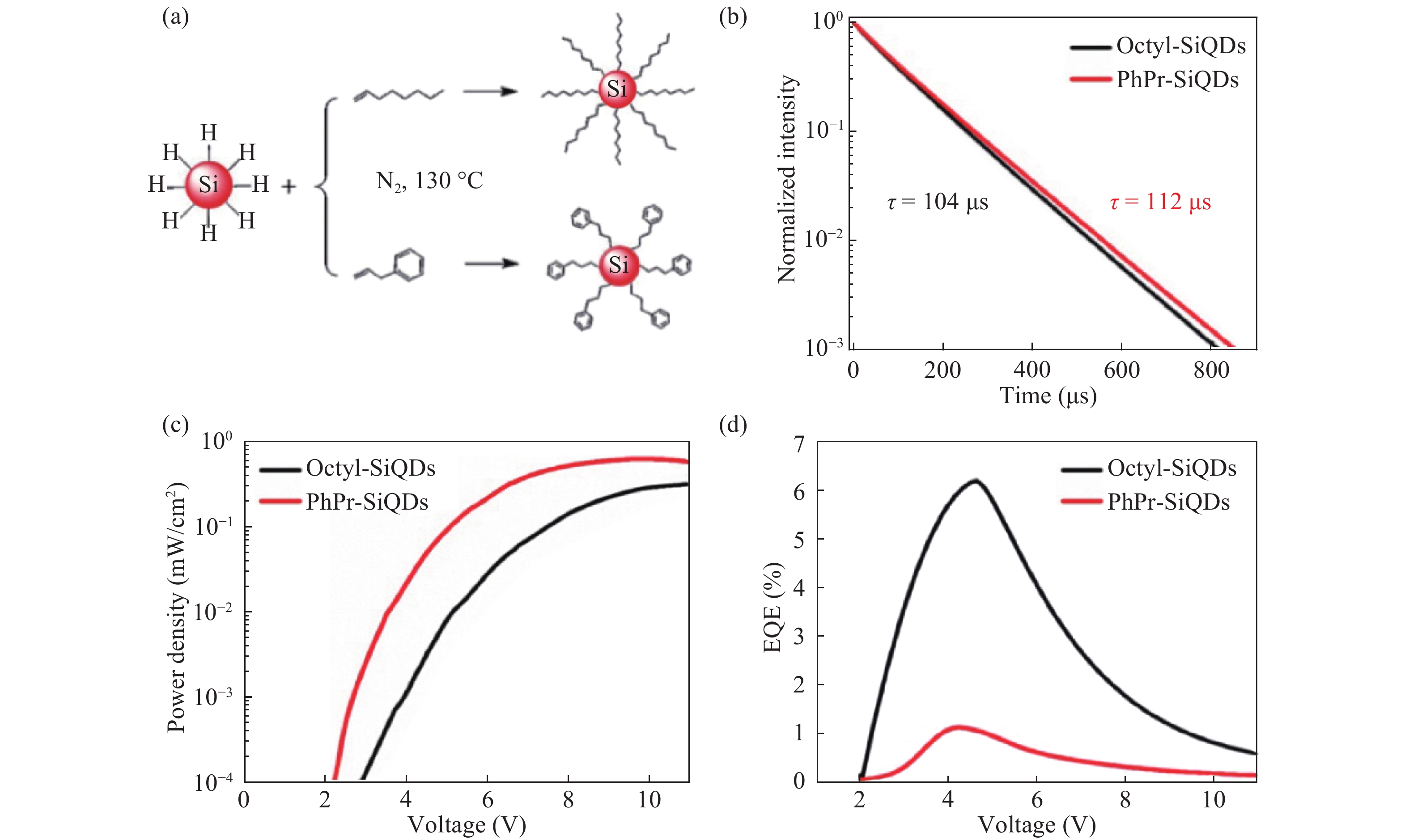
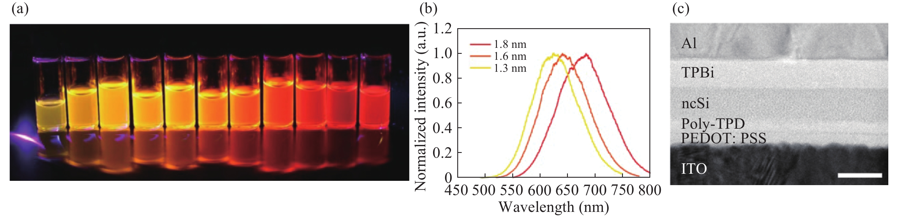
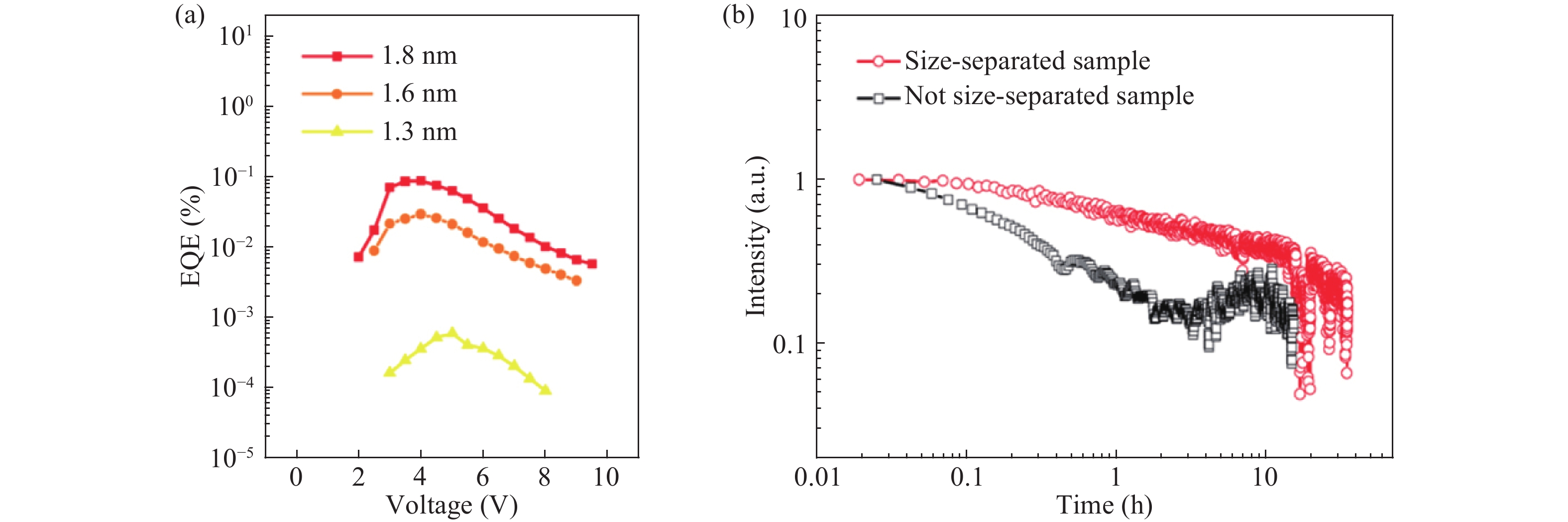
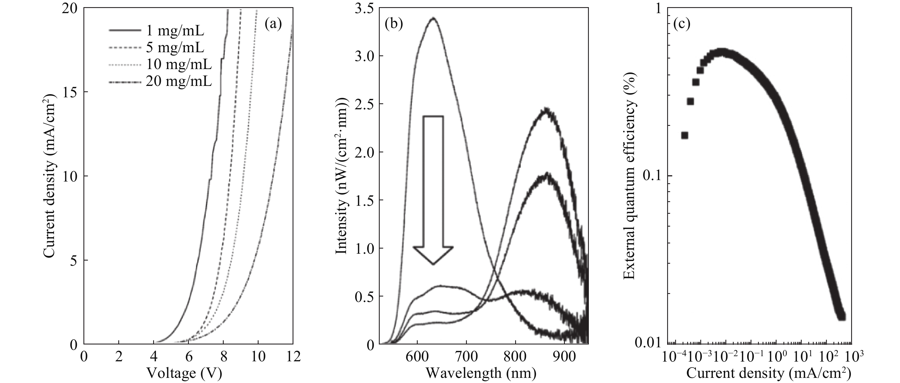
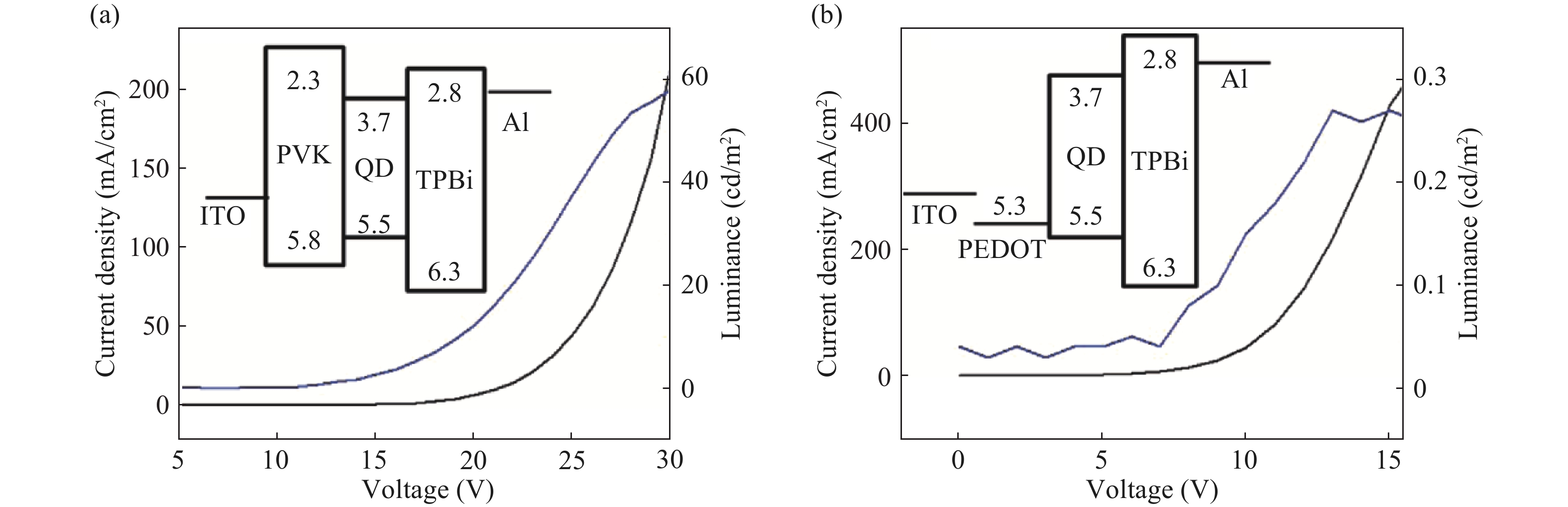
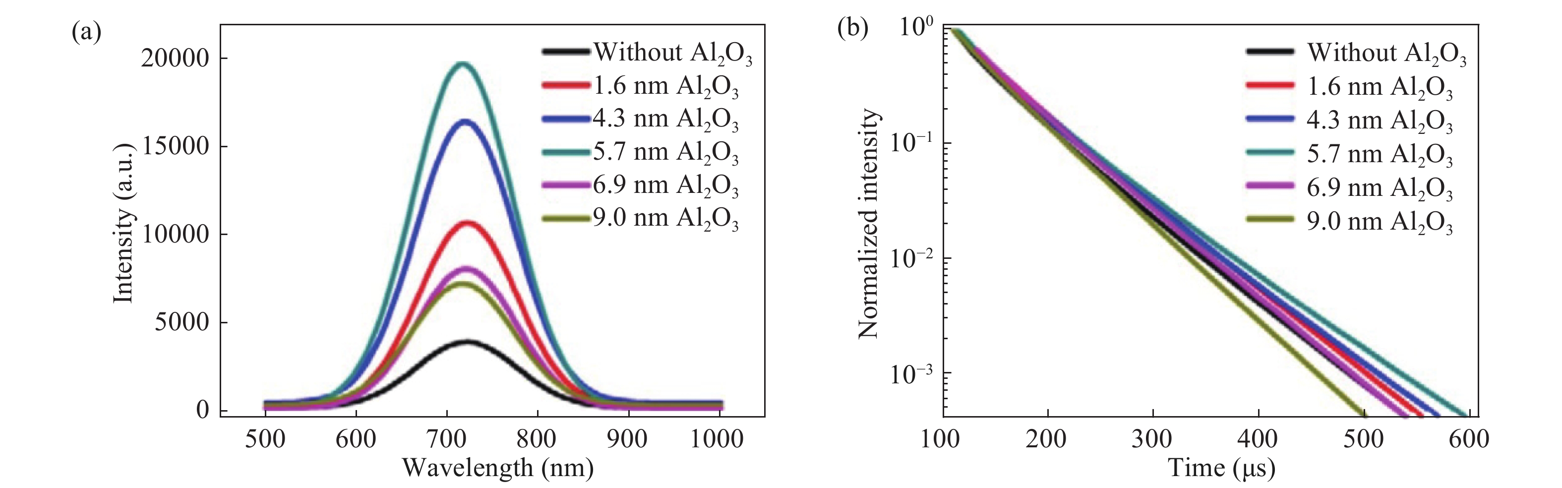
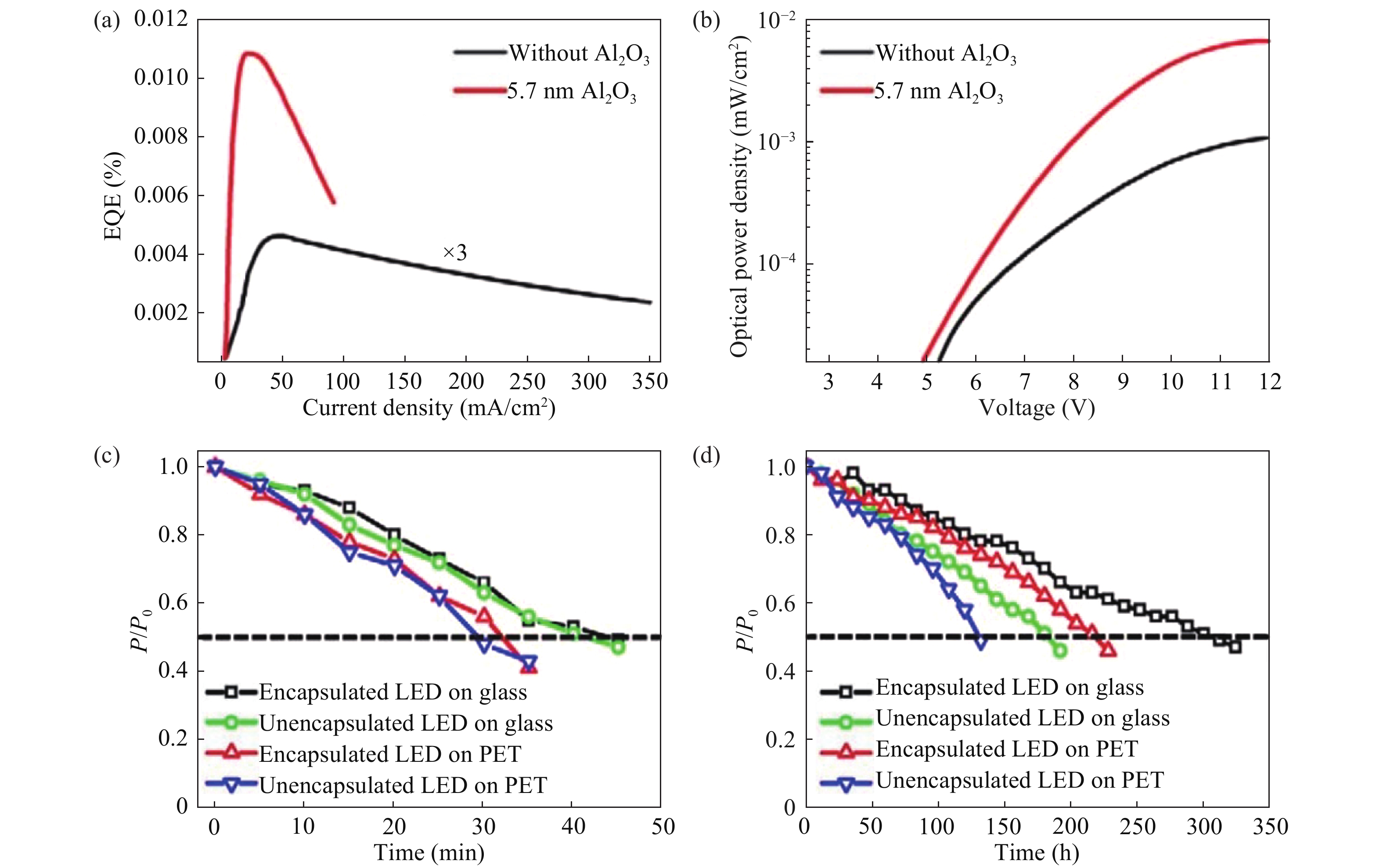
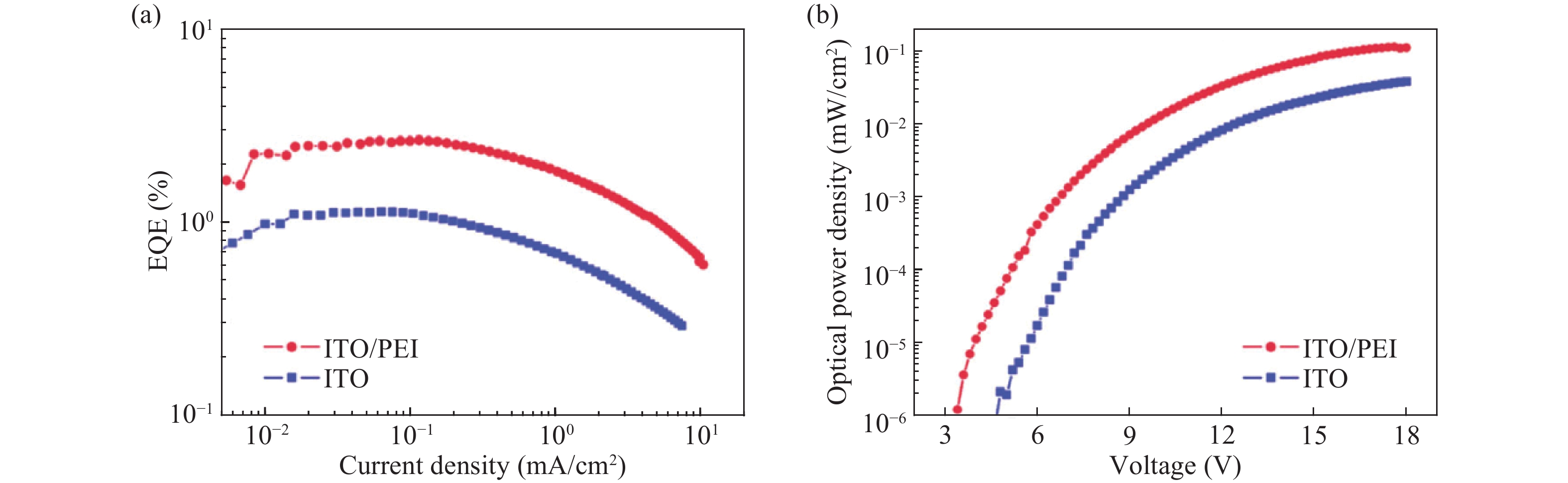
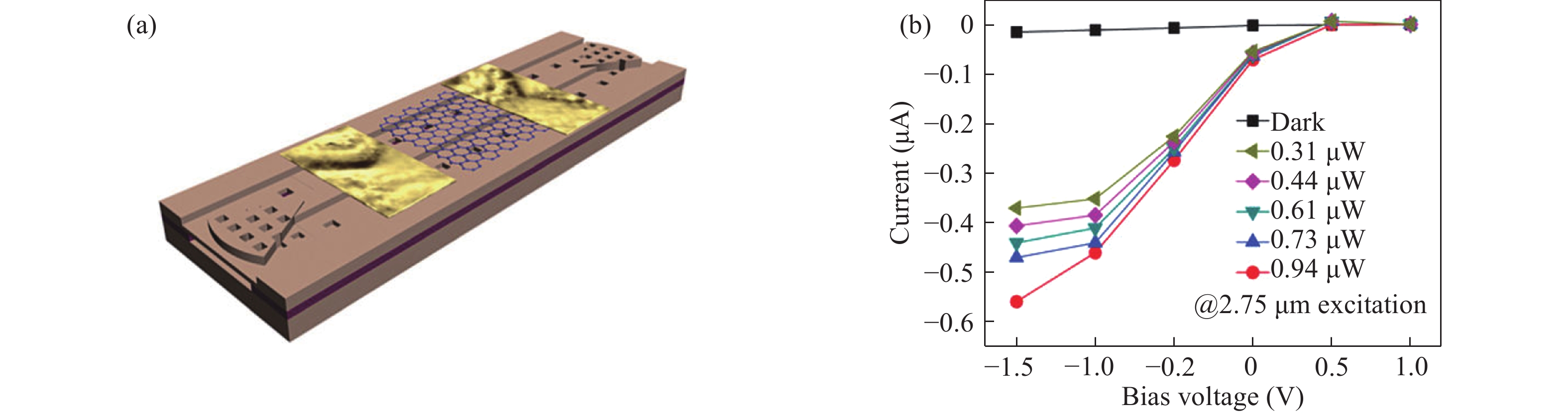
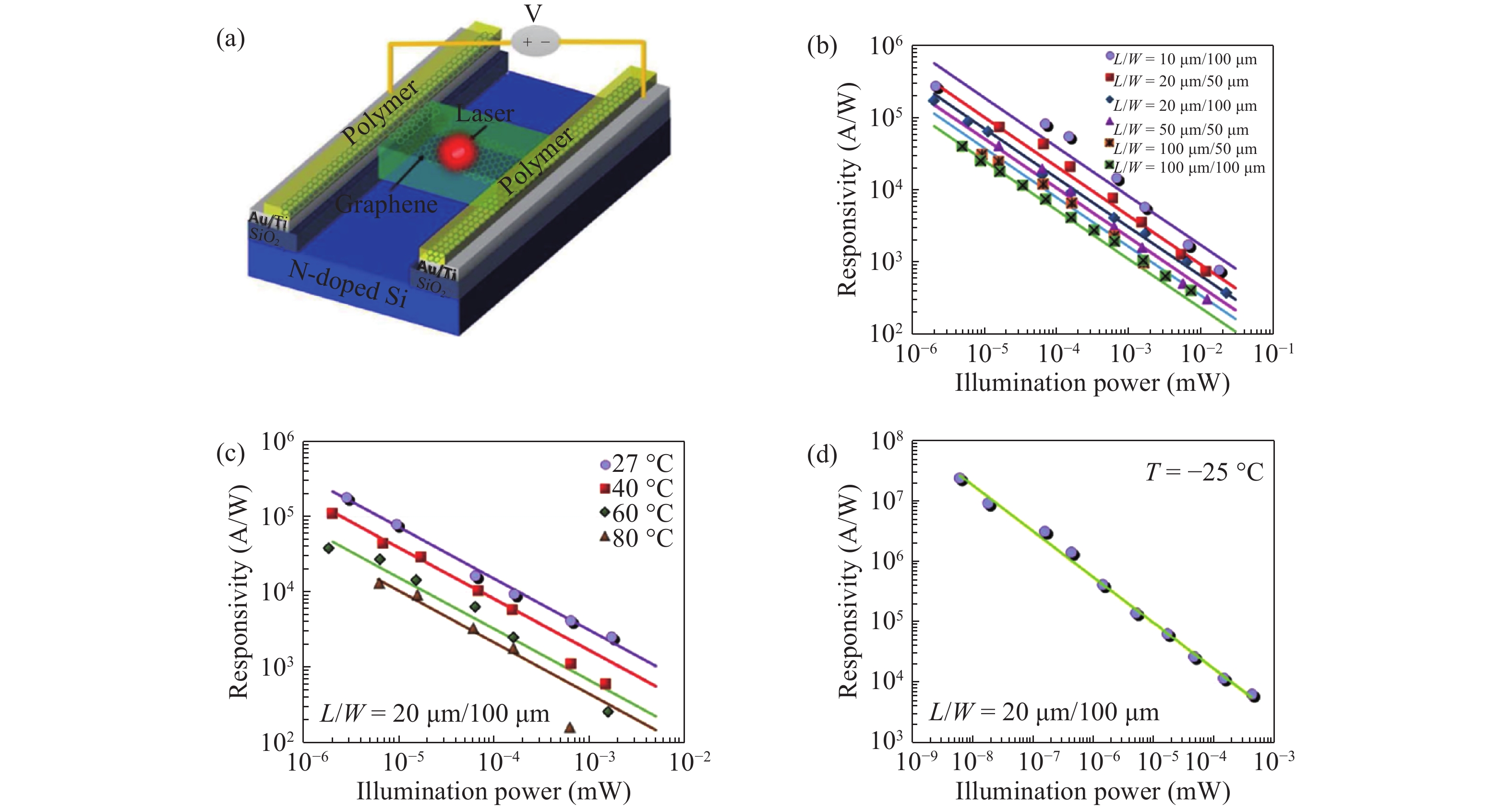
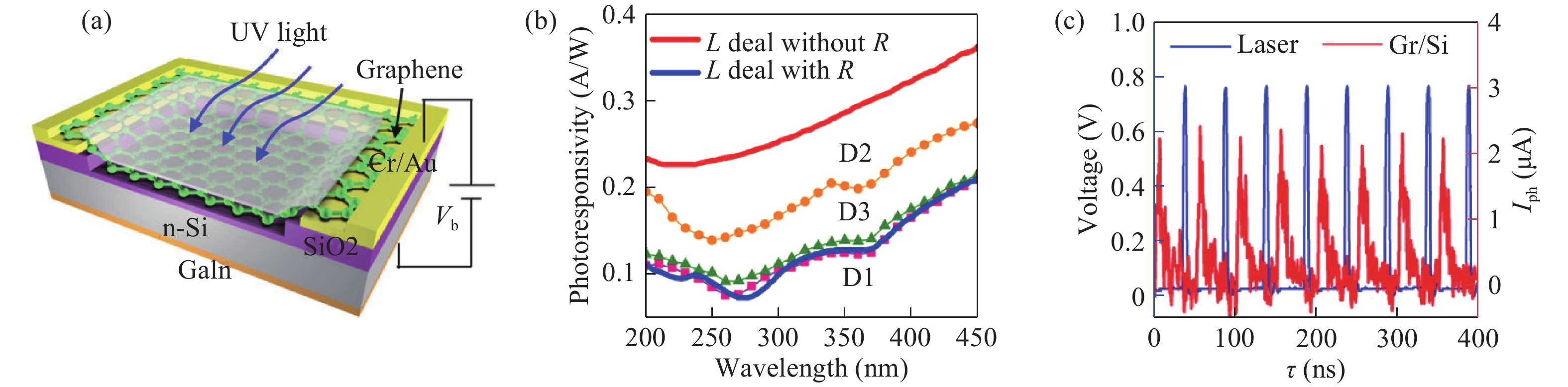
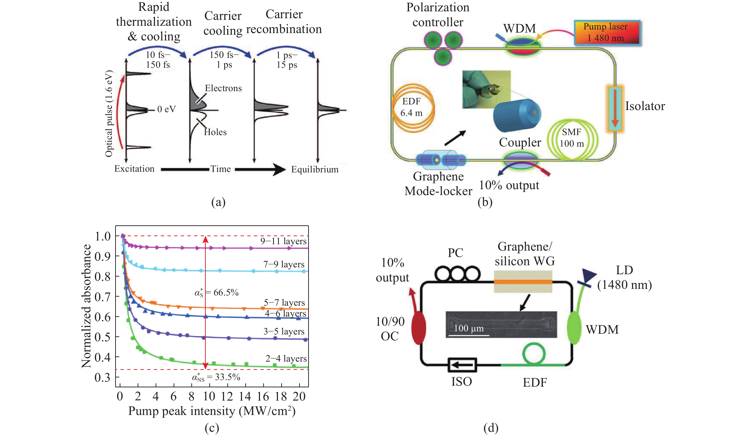
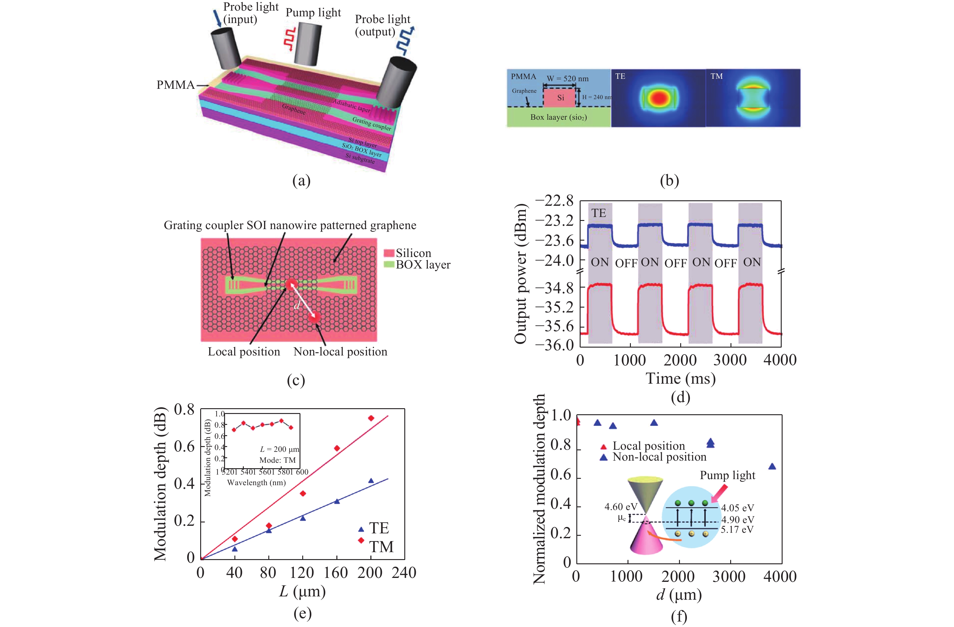
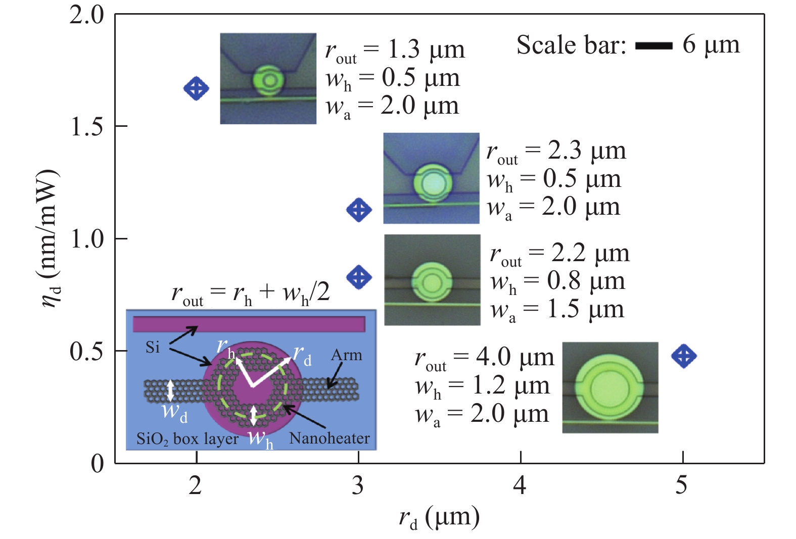
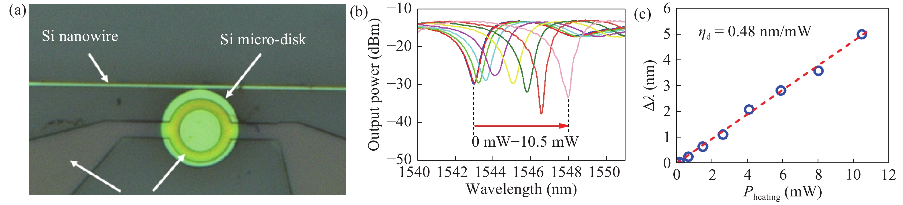
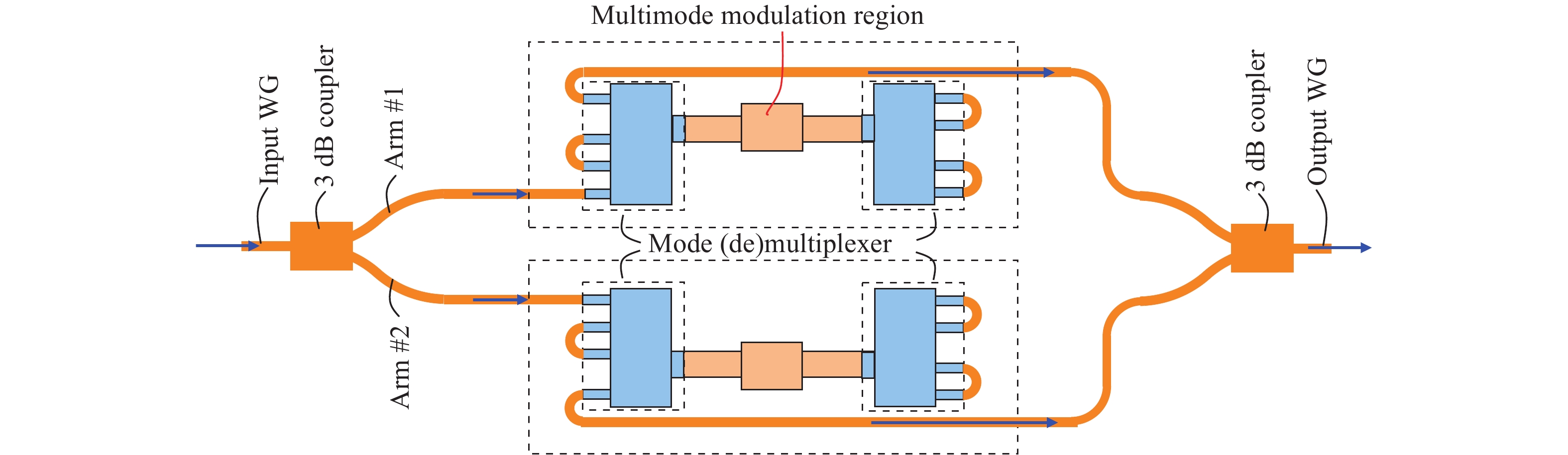
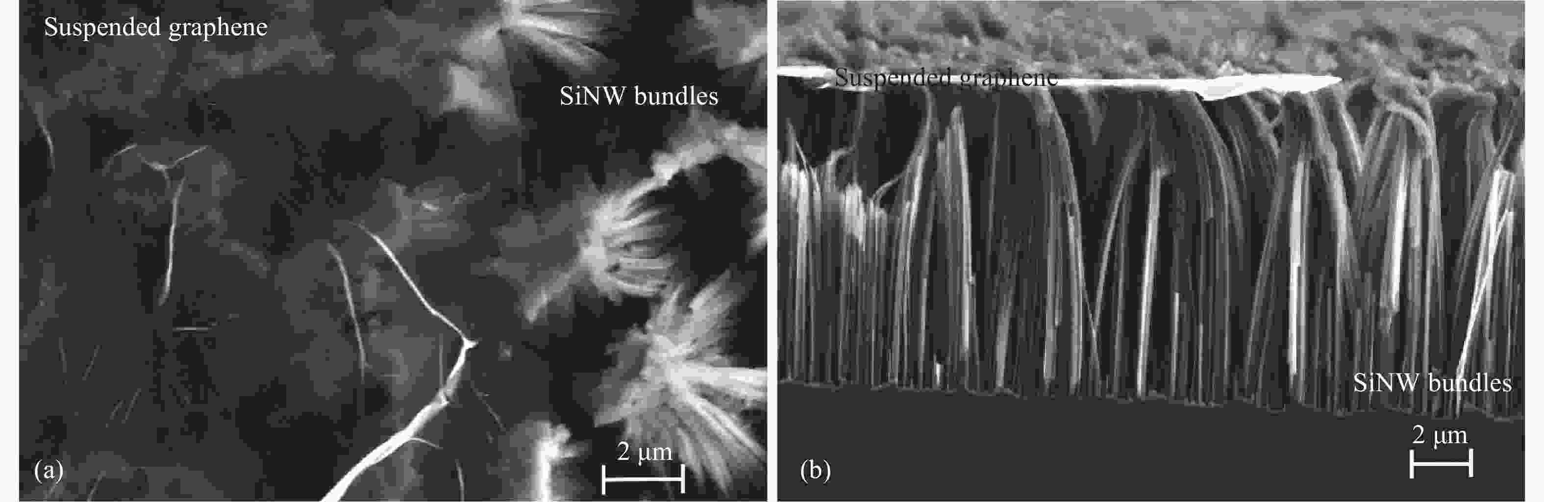
Silicon photonics for synergistic electronic–photonic integration has achieved remarkable progress in the past two decades. Active photonic devices, including lasers, modulators, and photodetectors, are the key challenges for Si photonics to meet the requirement of high bandwidth and low power consumption in photonic datalinks. Here we review recent efforts and progress in high-performance active photonic devices on Si, focusing on emerging technologies beyond conventional foundry-ready Si photonics devices. For emerging laser sources, we will discuss recent progress towards efficient monolithic Ge lasers, mid-infrared GeSn lasers, and high-performance InAs quantum dot lasers on Si for data center applications in the near future. We will then review novel modulator materials and devices beyond the free carrier plasma dispersion effect in Si, including GeSi and graphene electro-absorption modulators and plasmonic-organic electro-optical modulators, to achieve ultralow power and high speed modulation. Finally, we discuss emerging photodetectors beyond epitaxial Ge p–i–n photodiodes, including GeSn mid-infrared photodetectors, all-Si plasmonic Schottky infrared photodetectors, and Si quanta image sensors for non-avalanche, low noise single photon detection and photon counting. These emerging technologies, though still under development, could make a significant impact on the future of large-scale electronicSilicon photonics for synergistic electronic-photonic integration has achieved remarkable progress in the past two decades. Active photonic devices, including lasers, modulators, and photodetectors, are the key challenges for Si photonics to meet the requirement of high bandwidth and low power consumption in photonic datalinks. Here we review recent efforts and progress in high-performance active photonic devices on Si, focusing on emerging technologies beyond conventional foundry-ready Si photonics devices. For emerging laser sources, we will discuss recent progress towards efficient monolithic Ge lasers, mid-infrared GeSn lasers, and high-performance InAs quantum dot lasers on Si for data center applications in the near future. We will then review novel modulator materials and devices beyond the free carrier plasma dispersion effect in Si, including GeSi and graphene electro-absorption modulators and plasmonic-organic electro–optical modulators, to achieve ultralow power and high speed modulation. Finally, we discuss emerging photodetectors beyond epitaxial Ge p–i–n photodiodes, including GeSn mid-infrared photodetectors, all-Si plasmonic Schottky infrared photodetectors, and Si quanta image sensors for non-avalanche, low noise single photon detection and photon counting. These emerging technologies, though still under development, could make a significant impact on the future of large-scale electronic–photonic integration with performance inaccessible from conventional Si photonics technologies-photonic integration with performance inaccessible from conventional Si photonics technologies.
Silicon photonics for synergistic electronic–photonic integration has achieved remarkable progress in the past two decades. Active photonic devices, including lasers, modulators, and photodetectors, are the key challenges for Si photonics to meet the requirement of high bandwidth and low power consumption in photonic datalinks. Here we review recent efforts and progress in high-performance active photonic devices on Si, focusing on emerging technologies beyond conventional foundry-ready Si photonics devices. For emerging laser sources, we will discuss recent progress towards efficient monolithic Ge lasers, mid-infrared GeSn lasers, and high-performance InAs quantum dot lasers on Si for data center applications in the near future. We will then review novel modulator materials and devices beyond the free carrier plasma dispersion effect in Si, including GeSi and graphene electro-absorption modulators and plasmonic-organic electro-optical modulators, to achieve ultralow power and high speed modulation. Finally, we discuss emerging photodetectors beyond epitaxial Ge p–i–n photodiodes, including GeSn mid-infrared photodetectors, all-Si plasmonic Schottky infrared photodetectors, and Si quanta image sensors for non-avalanche, low noise single photon detection and photon counting. These emerging technologies, though still under development, could make a significant impact on the future of large-scale electronicSilicon photonics for synergistic electronic-photonic integration has achieved remarkable progress in the past two decades. Active photonic devices, including lasers, modulators, and photodetectors, are the key challenges for Si photonics to meet the requirement of high bandwidth and low power consumption in photonic datalinks. Here we review recent efforts and progress in high-performance active photonic devices on Si, focusing on emerging technologies beyond conventional foundry-ready Si photonics devices. For emerging laser sources, we will discuss recent progress towards efficient monolithic Ge lasers, mid-infrared GeSn lasers, and high-performance InAs quantum dot lasers on Si for data center applications in the near future. We will then review novel modulator materials and devices beyond the free carrier plasma dispersion effect in Si, including GeSi and graphene electro-absorption modulators and plasmonic-organic electro–optical modulators, to achieve ultralow power and high speed modulation. Finally, we discuss emerging photodetectors beyond epitaxial Ge p–i–n photodiodes, including GeSn mid-infrared photodetectors, all-Si plasmonic Schottky infrared photodetectors, and Si quanta image sensors for non-avalanche, low noise single photon detection and photon counting. These emerging technologies, though still under development, could make a significant impact on the future of large-scale electronic–photonic integration with performance inaccessible from conventional Si photonics technologies-photonic integration with performance inaccessible from conventional Si photonics technologies.
X X Wang, J F Liu. Emerging technologies in Si active photonics[J]. J. Semicond., 2018, 39(6): 061001. doi: 10.1088/1674-4926/39/6/061001.