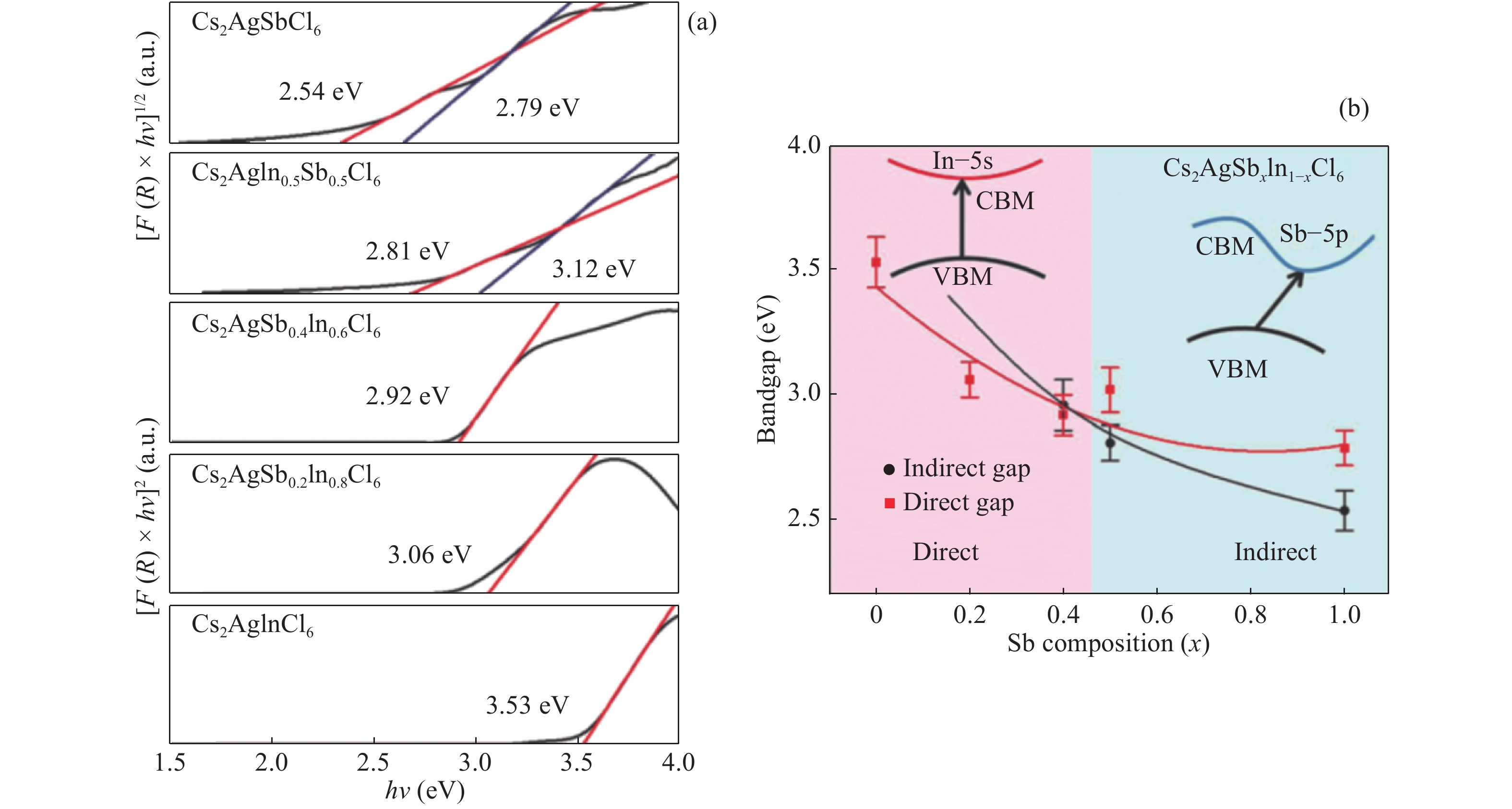
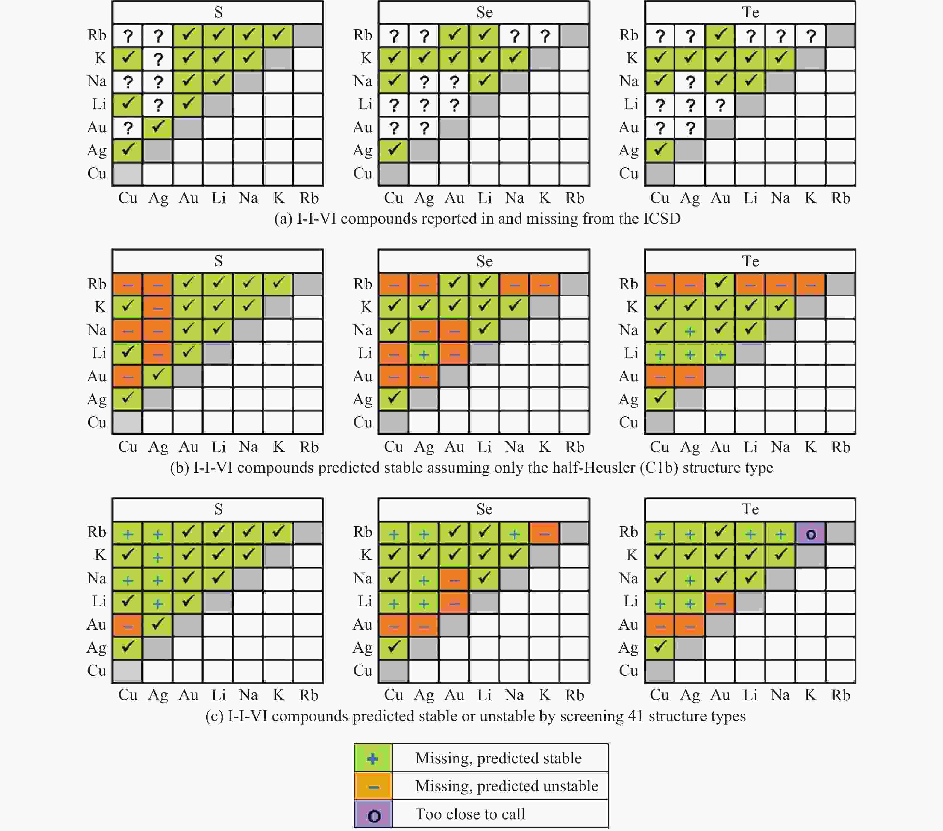
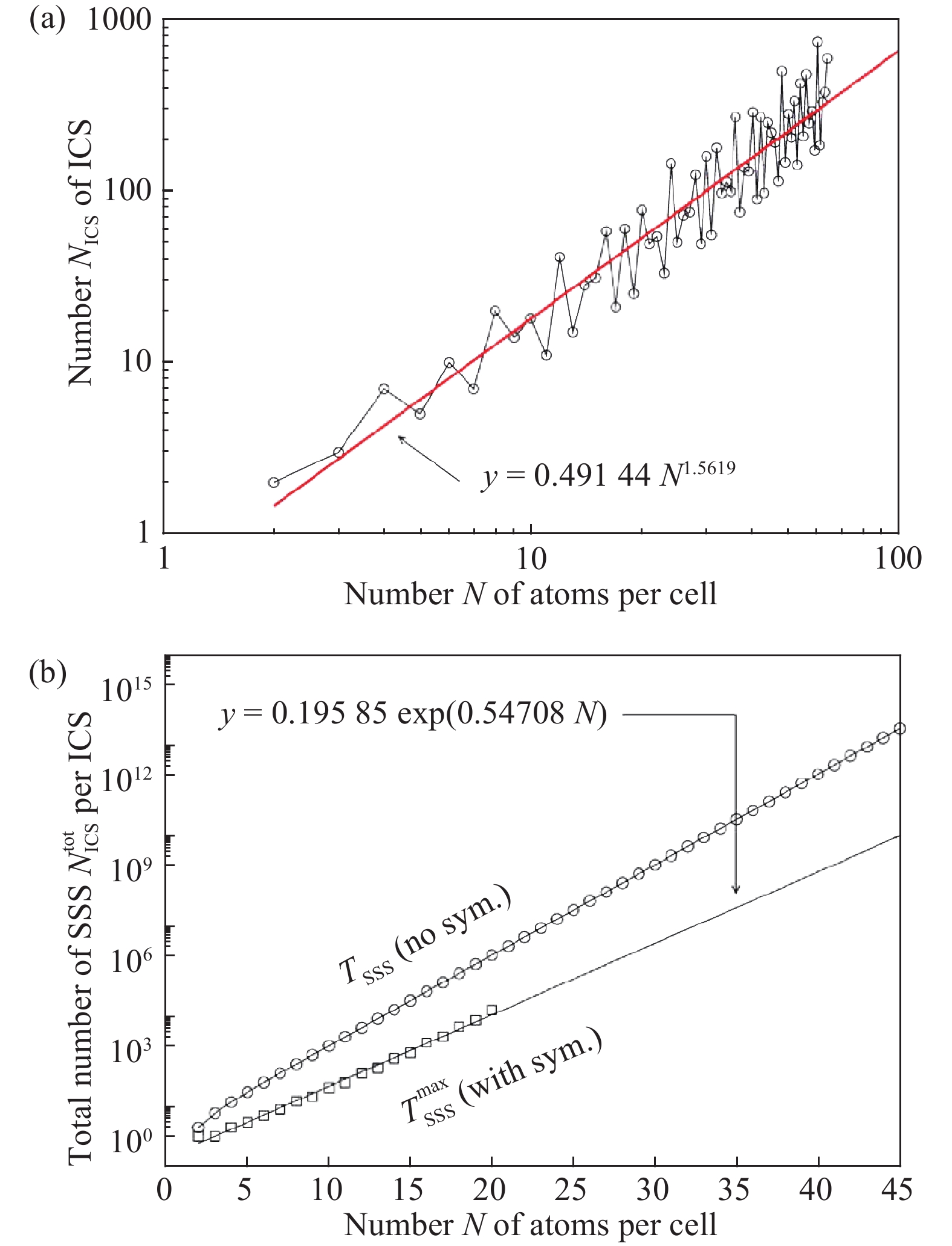
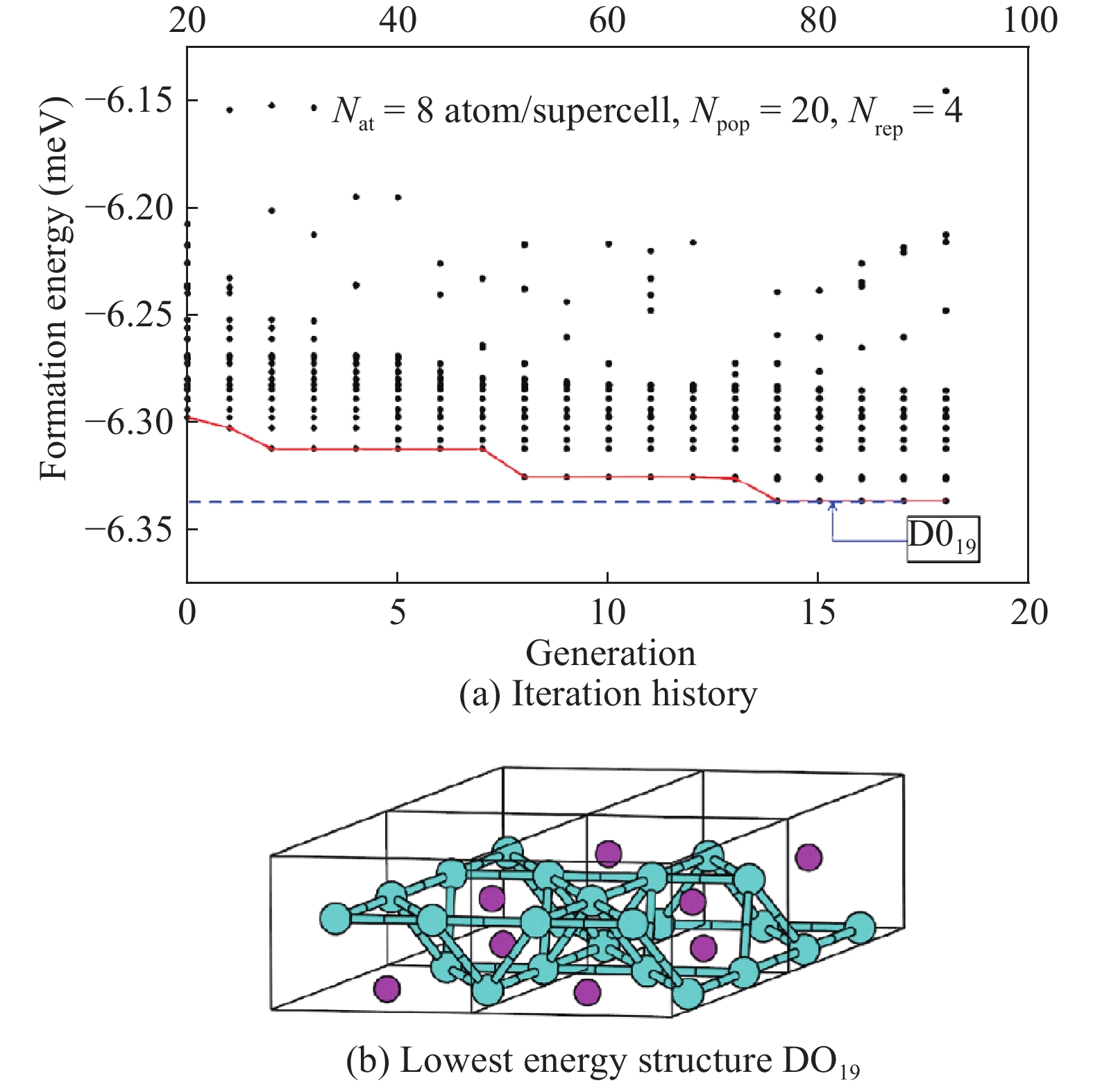
Advanced semiconducting materials have many applications in information technology and clean energy, thus they are critical to sustained economic and environmental development. However, in the past, many important technology-enabling materials were discovered by trial and error, which tends to take long time and high cost to discover and move them from research laboratory to market. Therefore, accelerating the pace of discovery and deployment of advanced semiconducting materials are crucial to achieving rapid development in the 21st century.In recent years, great progresses have been made in theory and computational algorithms to discover and design new functional materials using materials genome techniques and high-throughput calculations. These recent advances in the ability of new material discoveries have transformed our understanding of the field and provided both opportunity and challenge in developing new semiconductor technology.
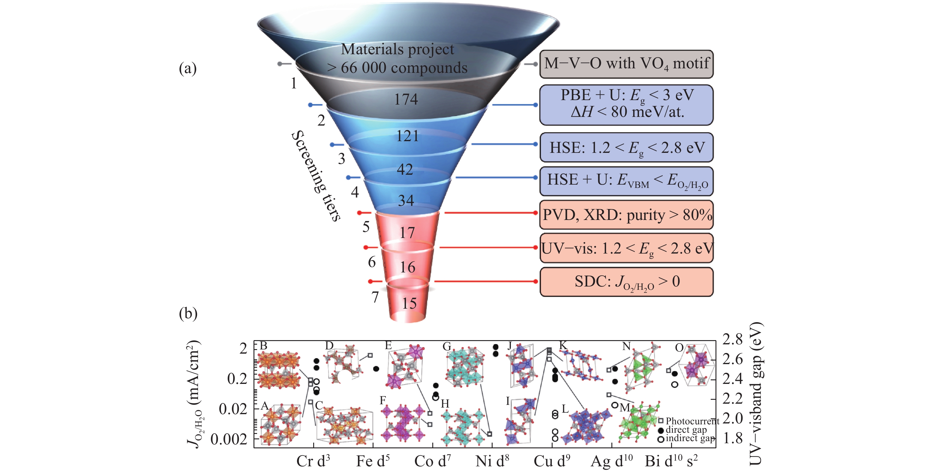
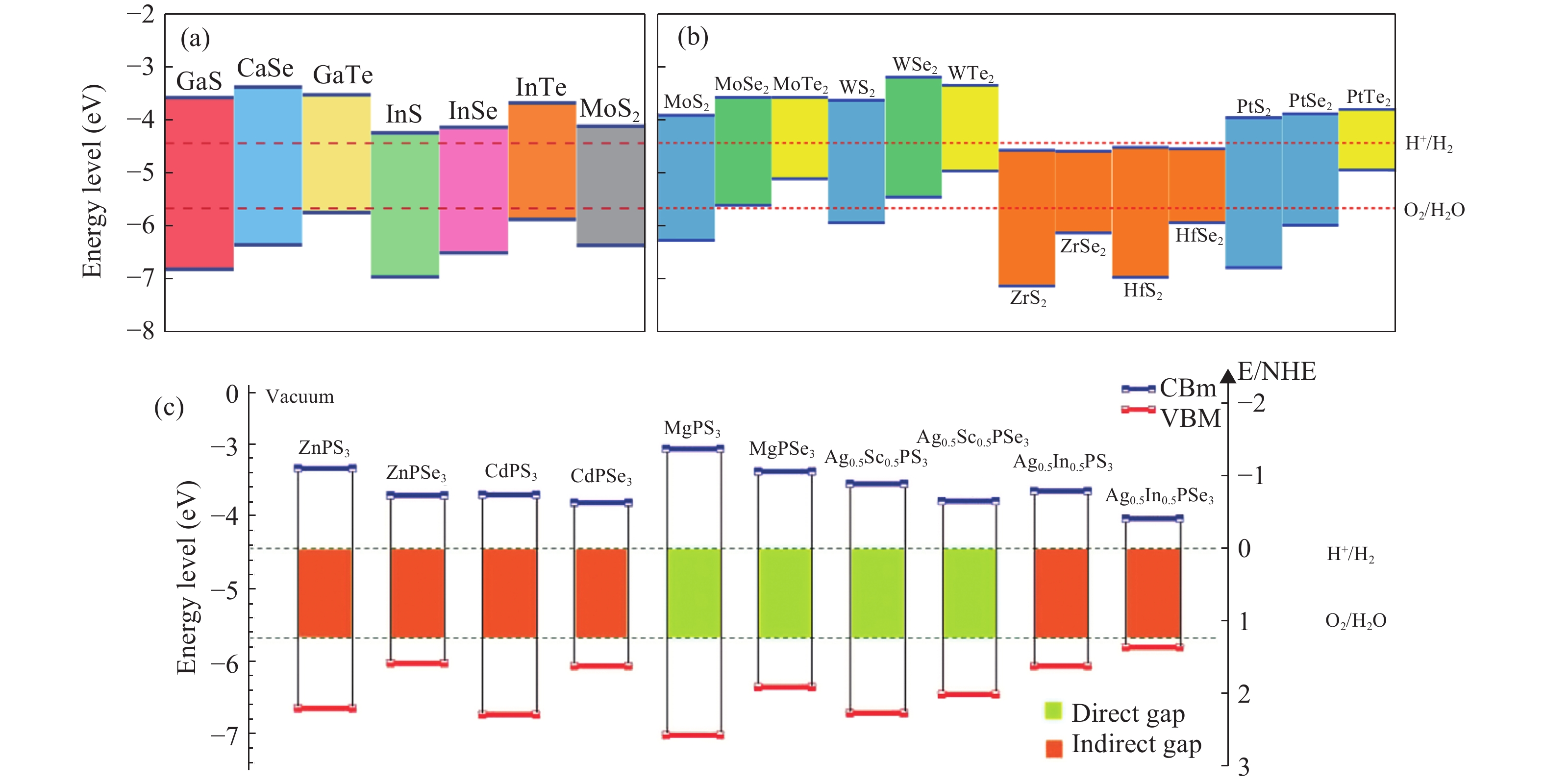
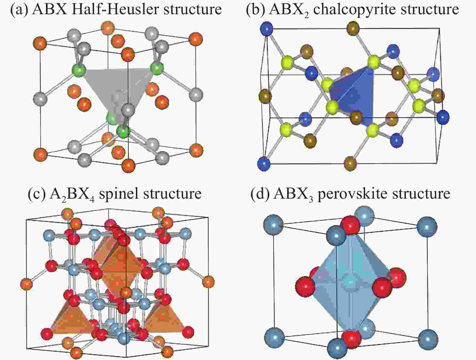
In this special topical issue, we invite leading scientists in this field to present their achievements and viewpoints as well as the state-of-the-art modelling methods on the material genome techniques, high-throughput calculations, machine learning, modeling and simulation of semiconducting materials.This special issue features four reviews ranging from data-driven material discovery for photocatalysis; approaches to design inorganic semiconductors while maintaining structural motifs; recent progress in Pb-free stable inorganic double halide perovskites; crystal structure prediction in the context of inverse materials design; and an article on first-principle high-throughput calculations of carrier effective masses of two-dimensional transition metal dichalcogenides.
We sincerely hope that this special issue could provide a valuable reference and perspective for the research community working in this exciting field and inspire many more to enter this field. We would like to thank all the authors who have contributed high-quality peer-reviewed articles to this special issue. We are also grateful to the editorial and production staff of Journal of Semiconductors for their superb assistance.