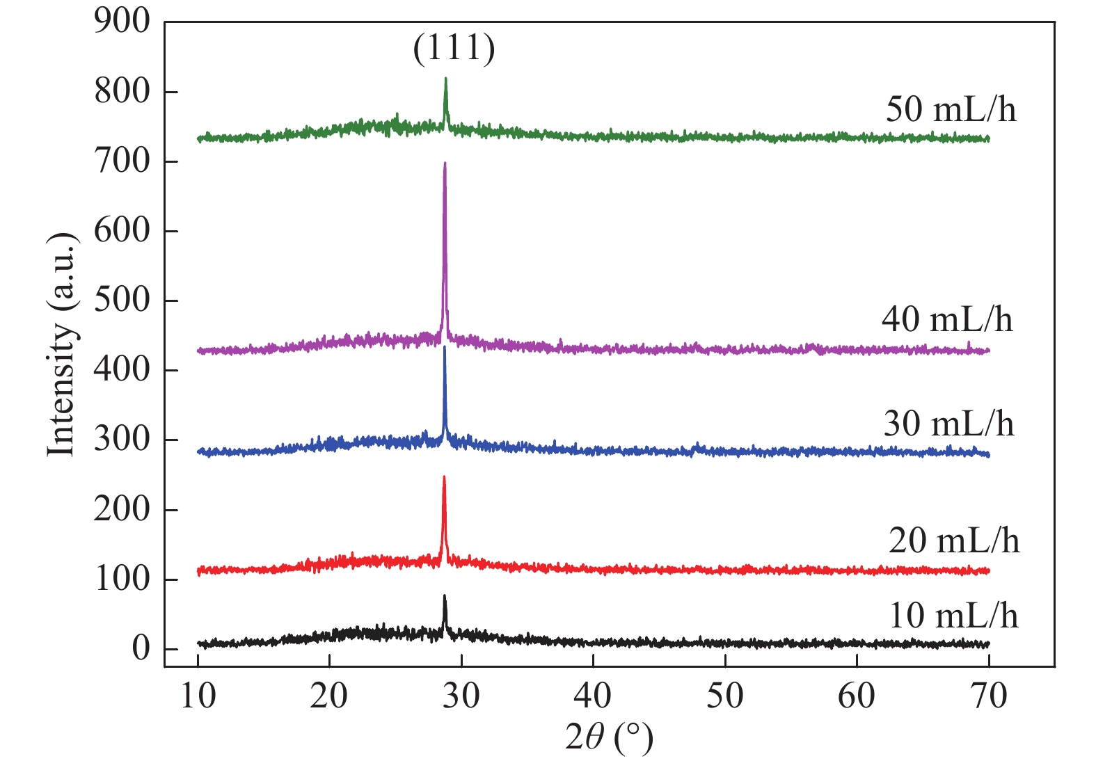
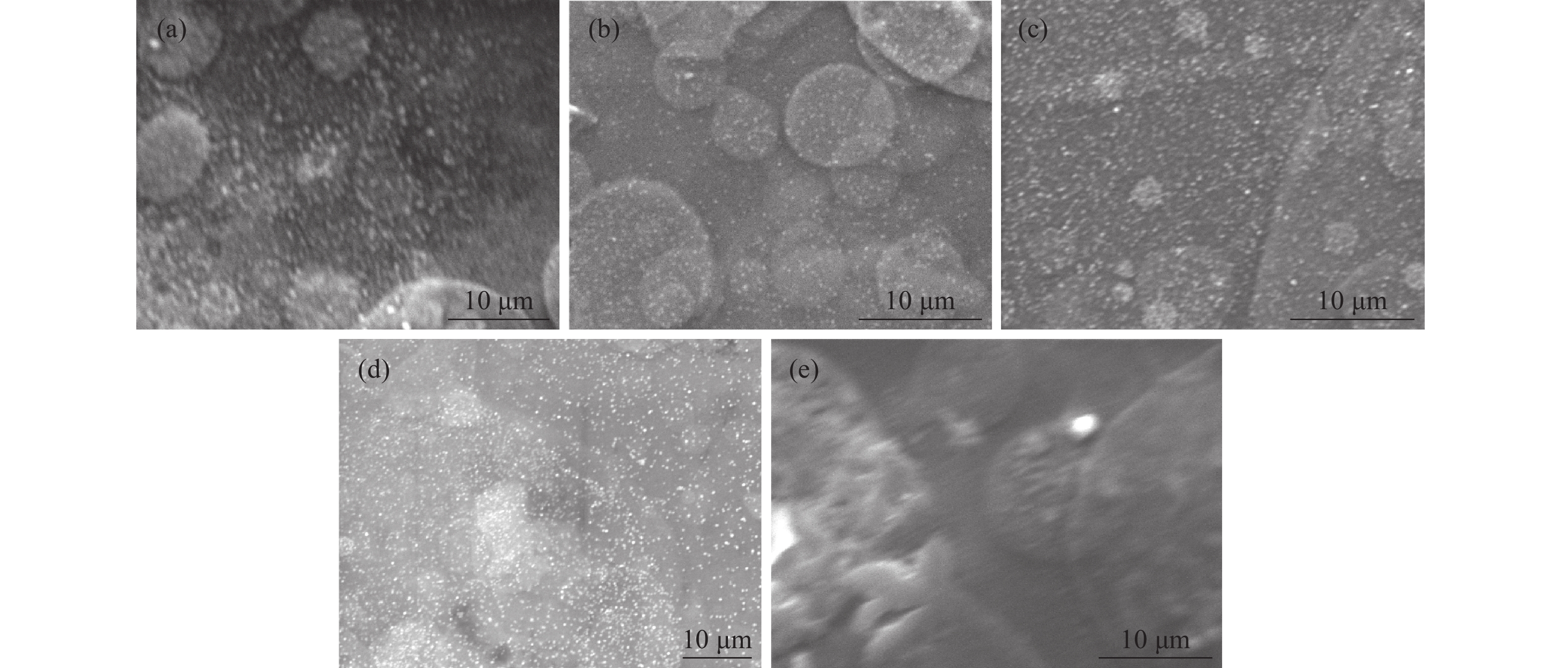
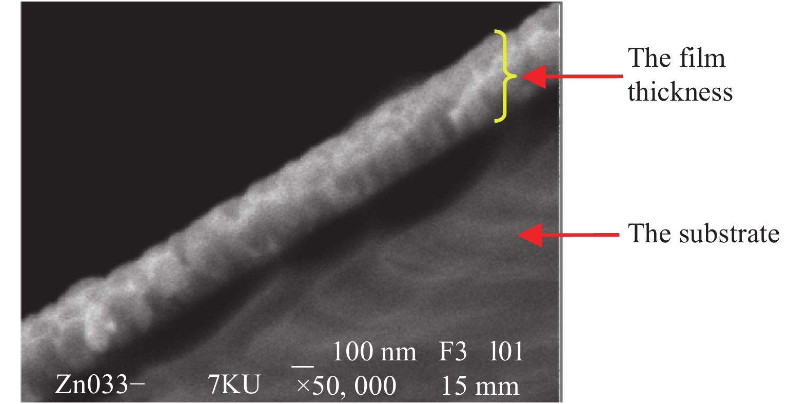
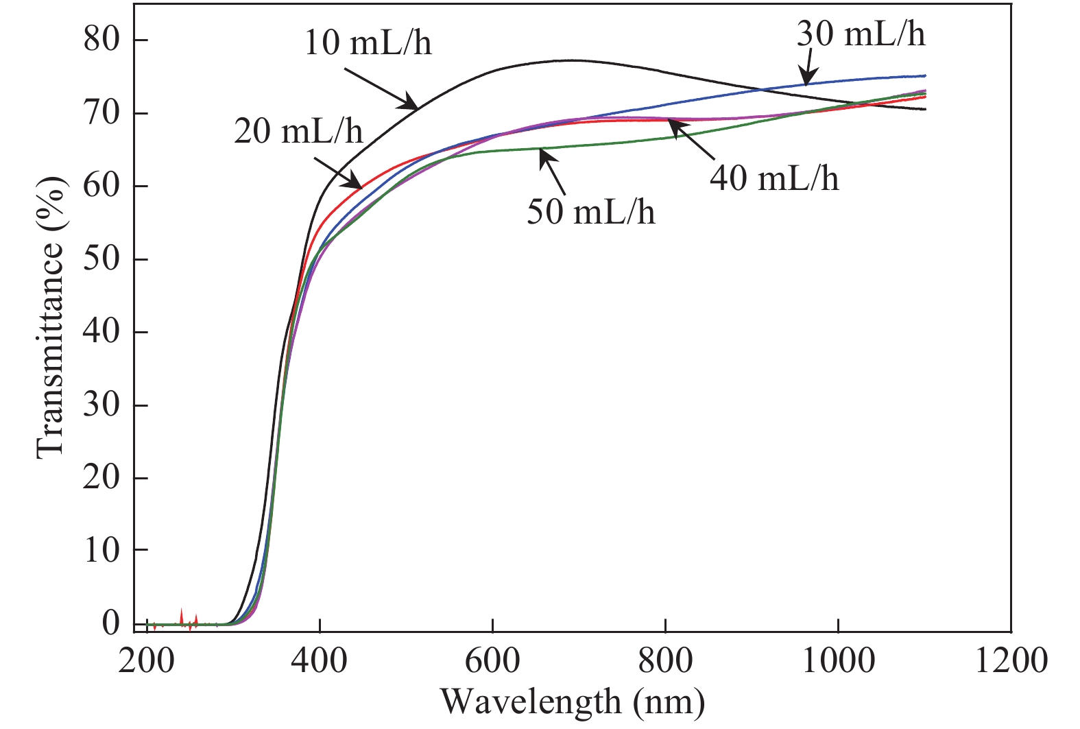
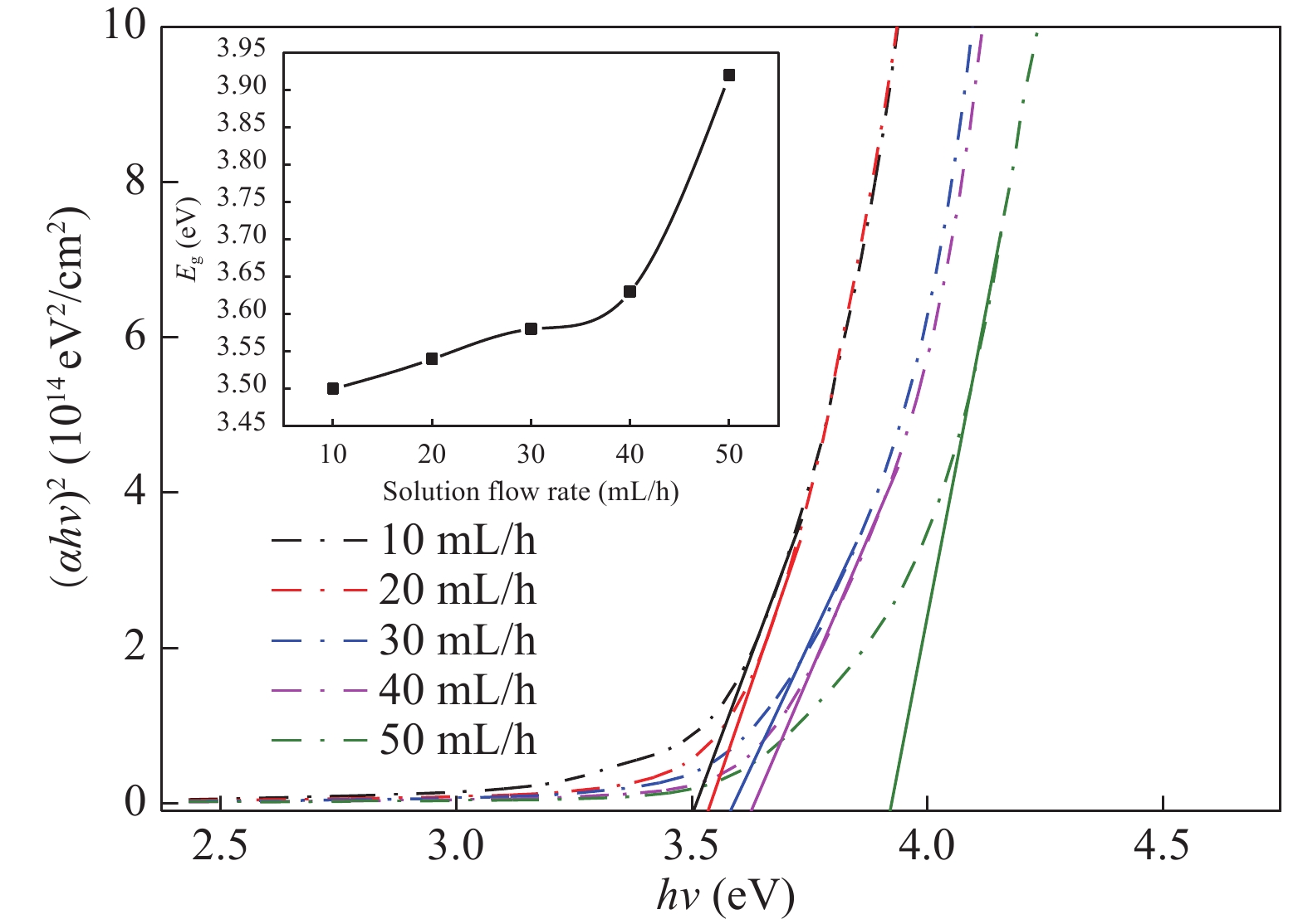
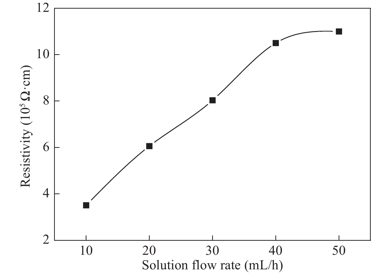
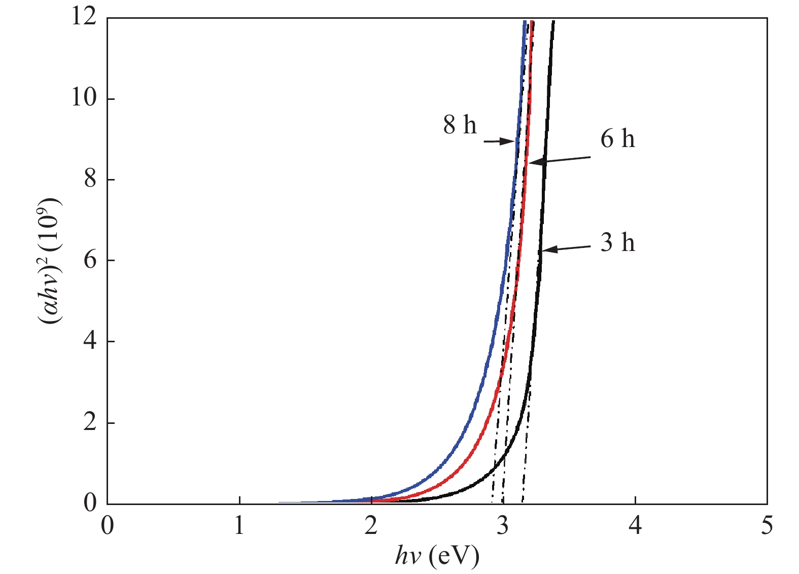
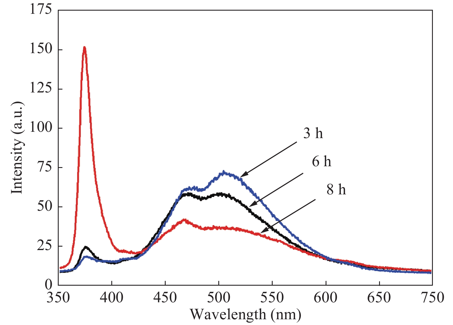
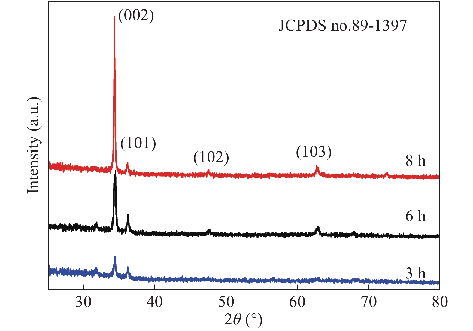
The aim of this work is to investigate the dependence of ZnS thin films structural and optical properties with the solution flow rate during the deposition using an ultrasonic spray method. The solution flow rate ranged from 10 to 50 mL/h and the substrate temperature was maintained at 450 °C. The effect of the solution flow rate on the properties of ZnS thin films was investigated by X-ray diffraction (XRD), scanning electron microscopy (SEM), optical transmittance spectroscopy (UV–V) and the four-point method. The X-ray diffraction analysis showed that the deposited material was pure zinc sulphide, it has a cubic sphalerite structure with preferential orientation along the (111) direction. The grain size values were calculated and found to be between 38 to 82 nm. SEM analysis revealed that the deposited thin films have good adherence to the substrate surfaces, are homogeneous and have high density. The average transmission of all films is up more than 65% in the range wavelength from 200 to 1100 nm and their band gap energy values were found between 3.5–3.92 eV. The obtained film thickness varies from 390 to 1040 nm. Moreover, the electric resistivity of the deposited films increases with the increasing of the solution flow rate between 3.51 × 10⁵ and 11 × 105 Ω·cm.


ZnO nanowires (NWs) layers have been synthesized using a two-step chemical solution method on ITO glass substrates coated with ZnO seeds at different immersing times. The structures, morphology and optical properties of the synthesized ZnO NWs have been investigated. The prepared ZnO NWs have an obvious polycrystalline hexangular wurtzite structure and are preferentially oriented along the c-axis (002). FESEM micrographs showed that the prepared ZnO NWs are close to being vertically grown and more densely at higher immersing times. Poly [2-methoxy-5(2′-ethyl-hexyloxy)-1,4-phenylenevinylene], MEH-PPV, was used as an active layer to prepare three samples of MEH-PPV/ZnO solar cell based on ZnO NWs that were prepared at different immersing times. A maximum power conversion efficiency of 0.812% was achieved for MEH-PPV/ZnO solar cell prepared at a higher immersing time. The improved efficiency may be attributed to the enhancement of both open-circuit voltage and fill factor.
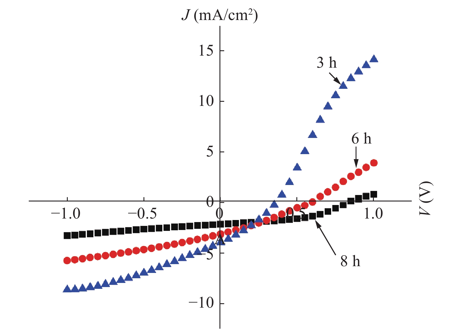
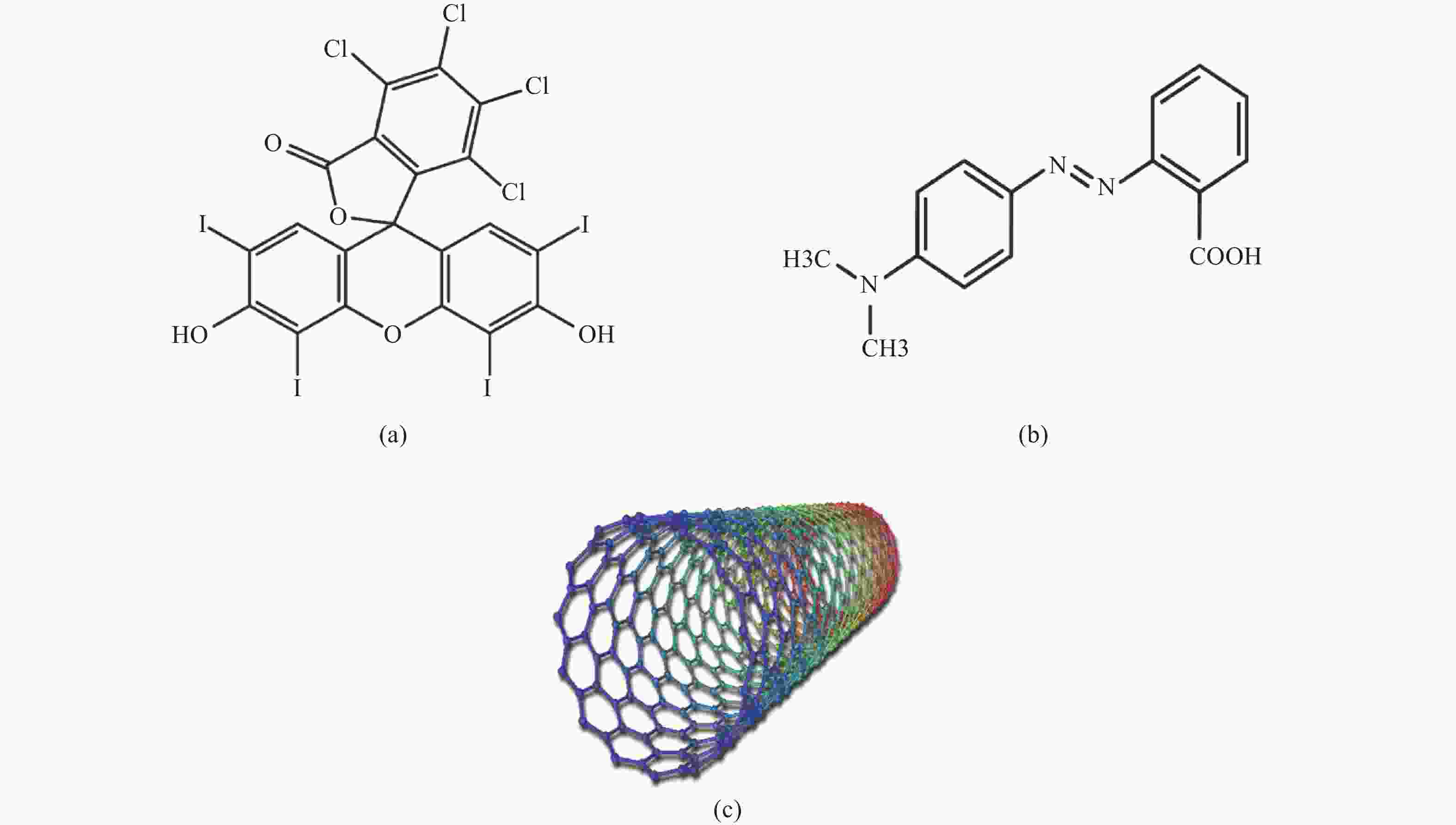
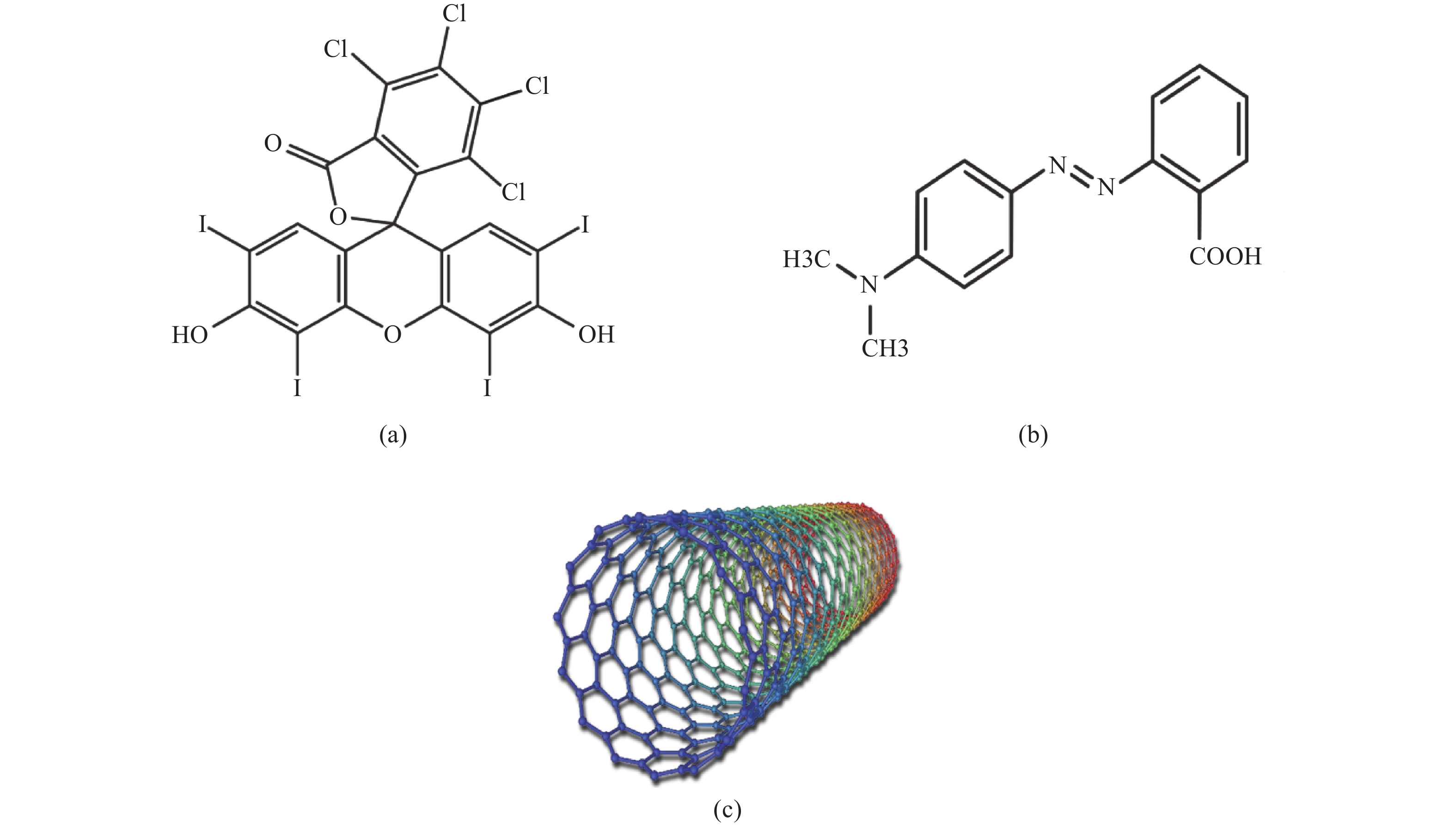
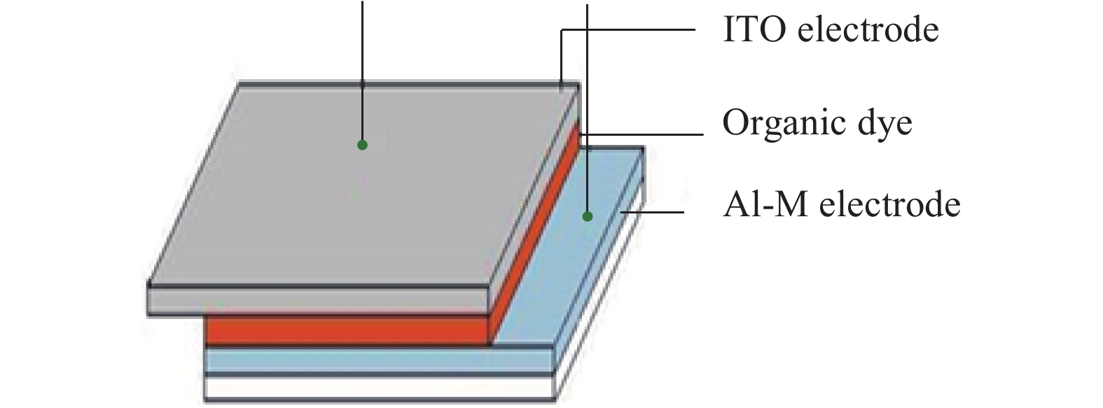
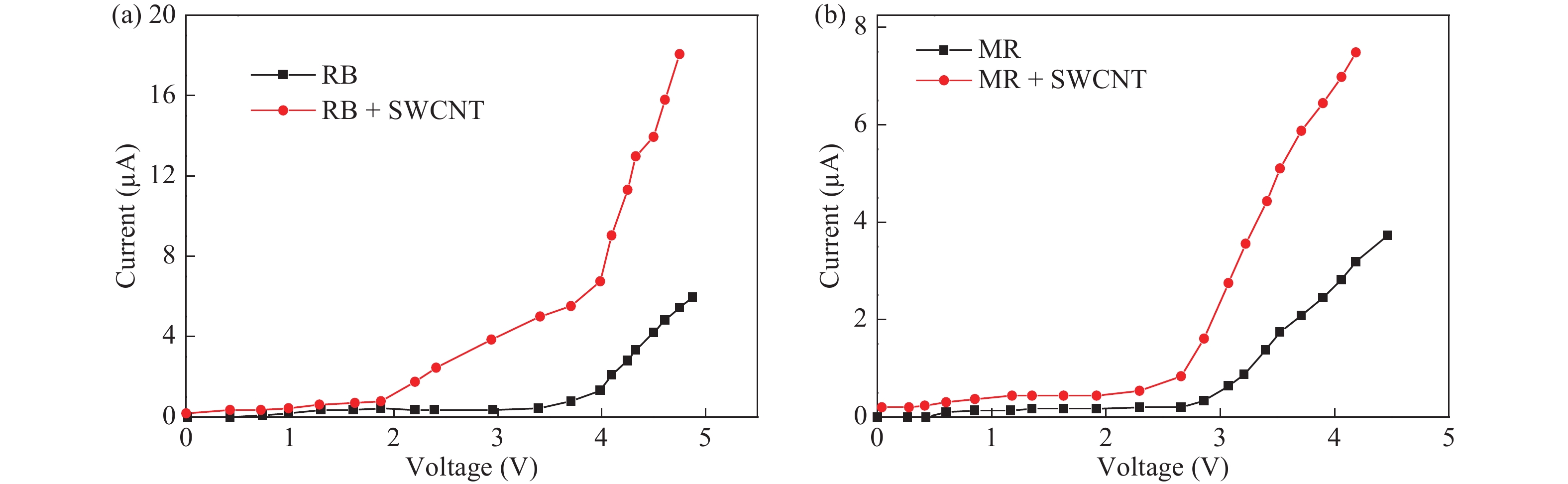
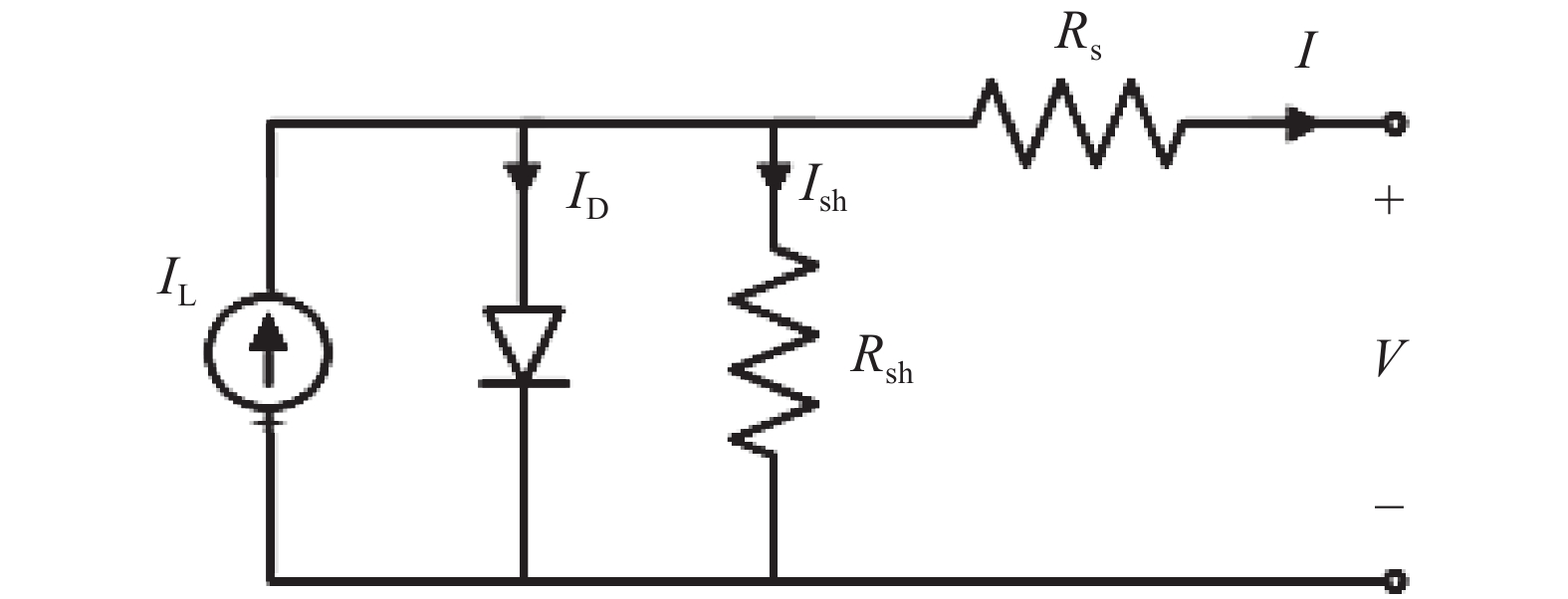
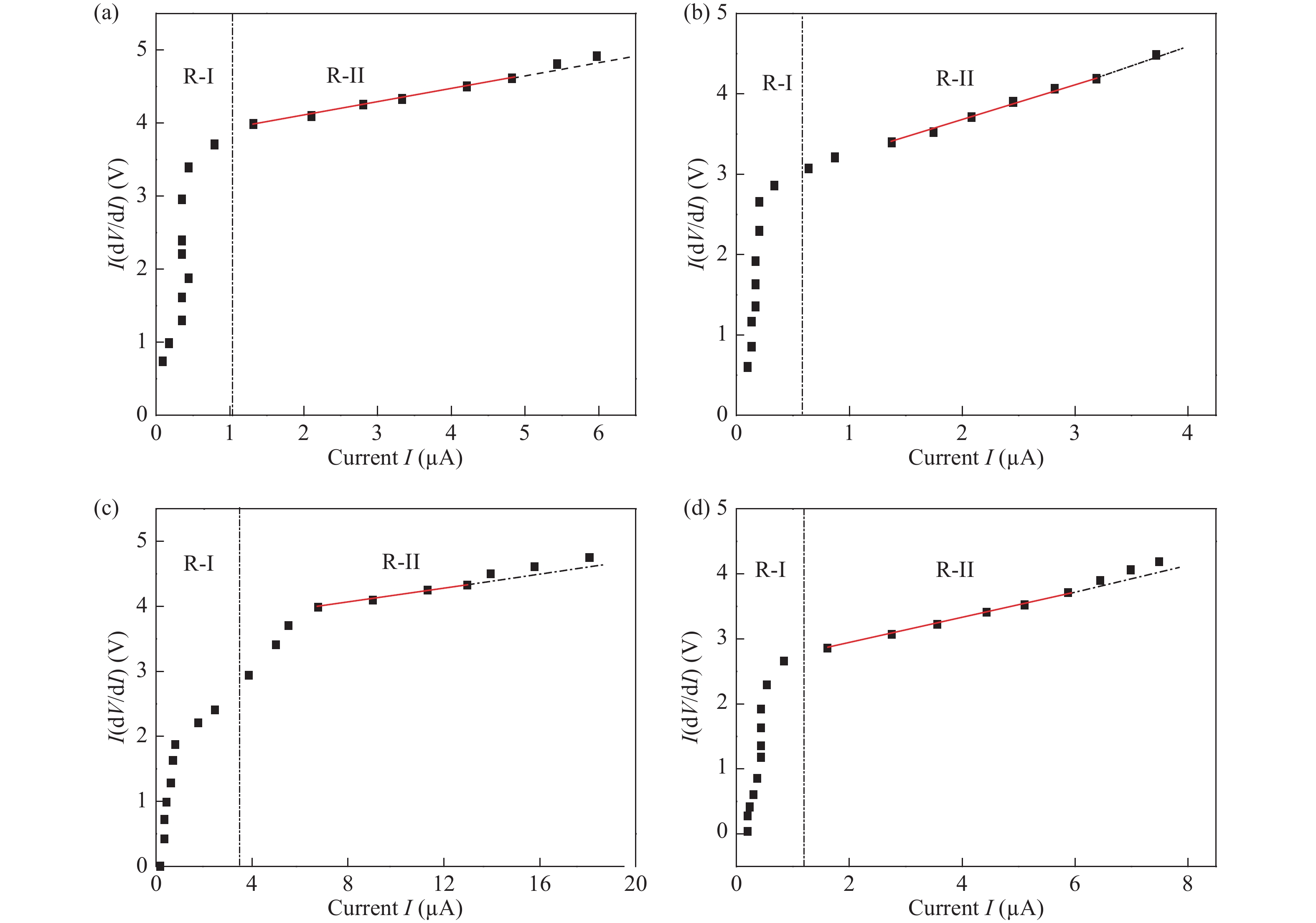
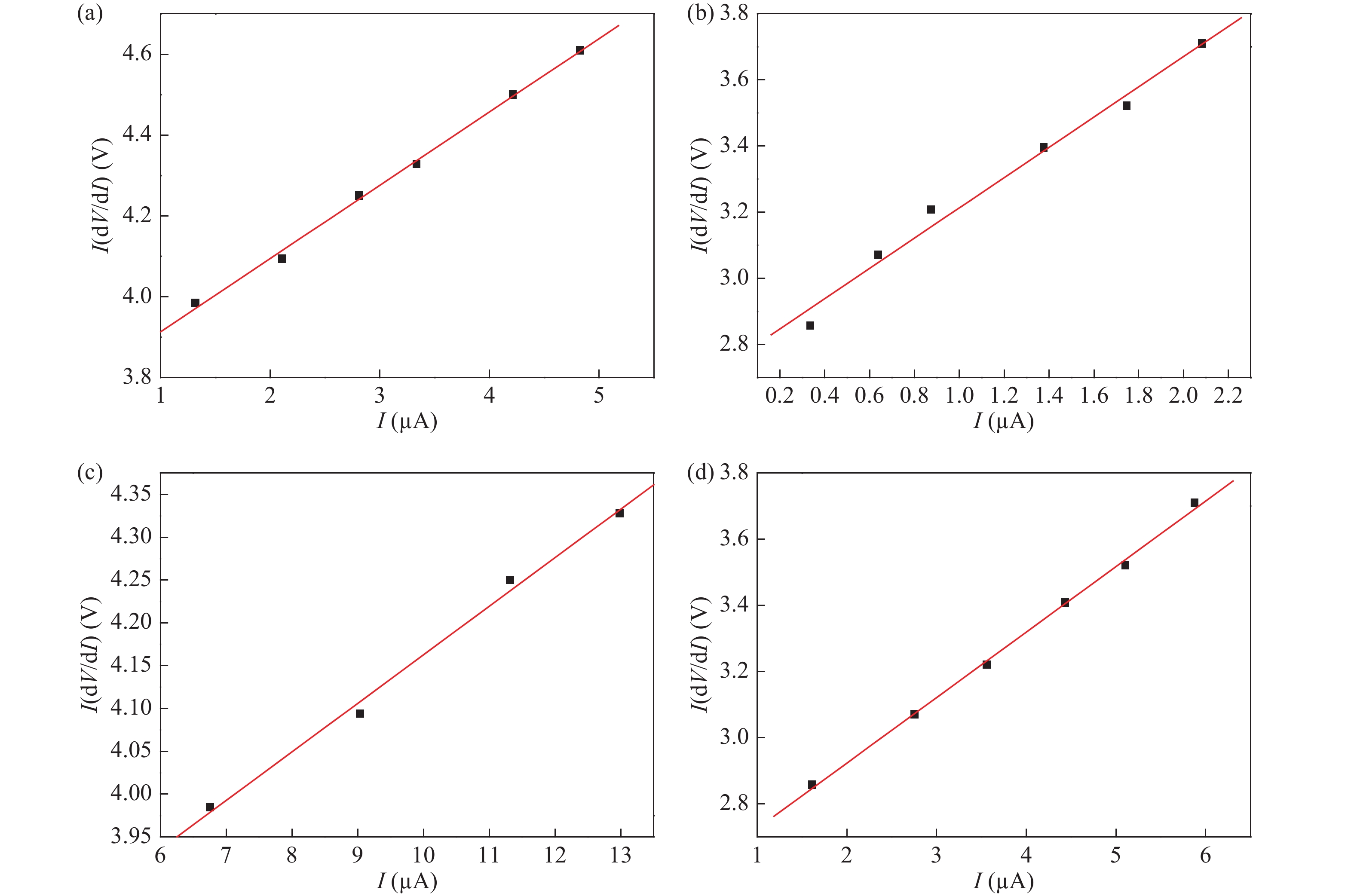
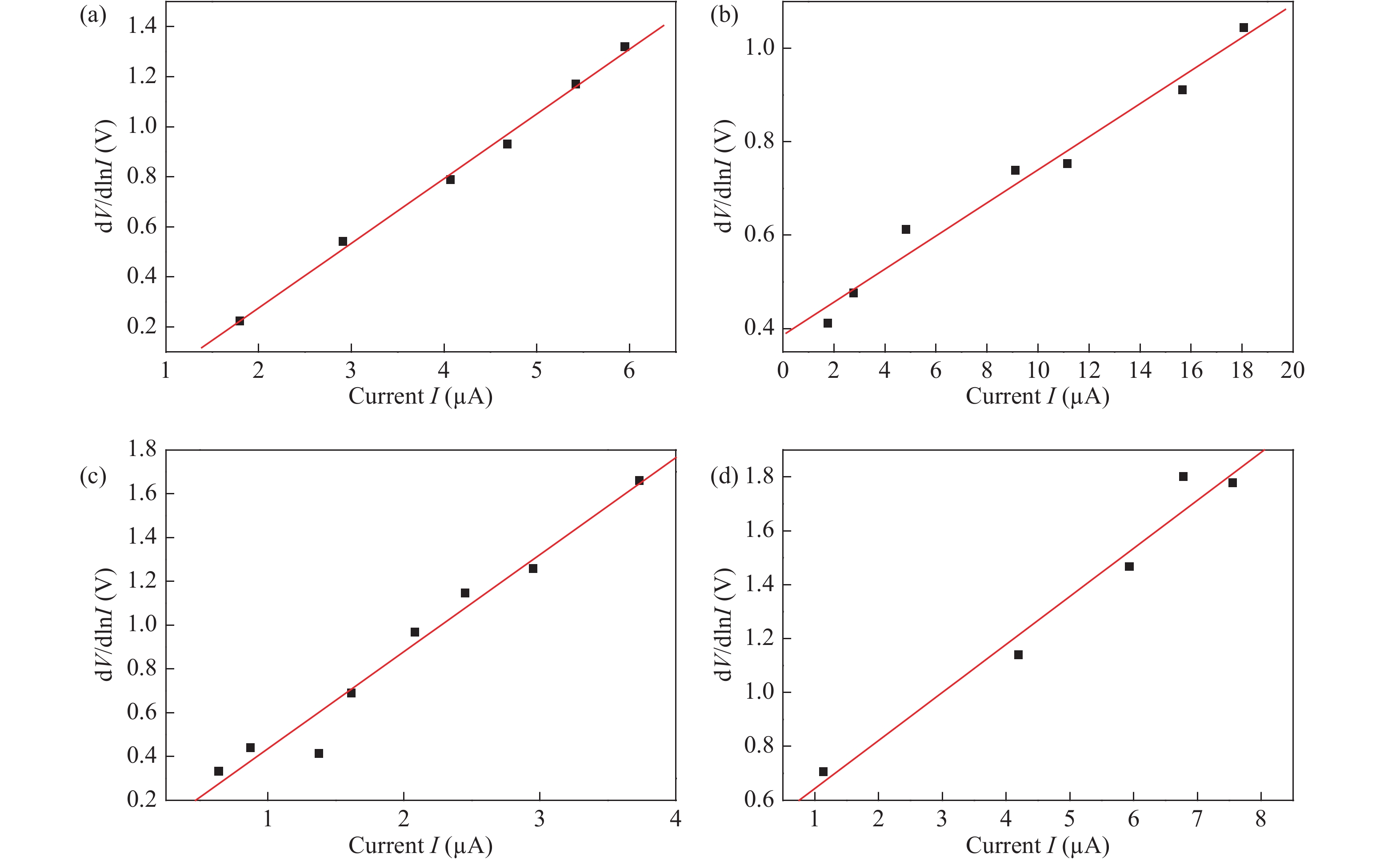
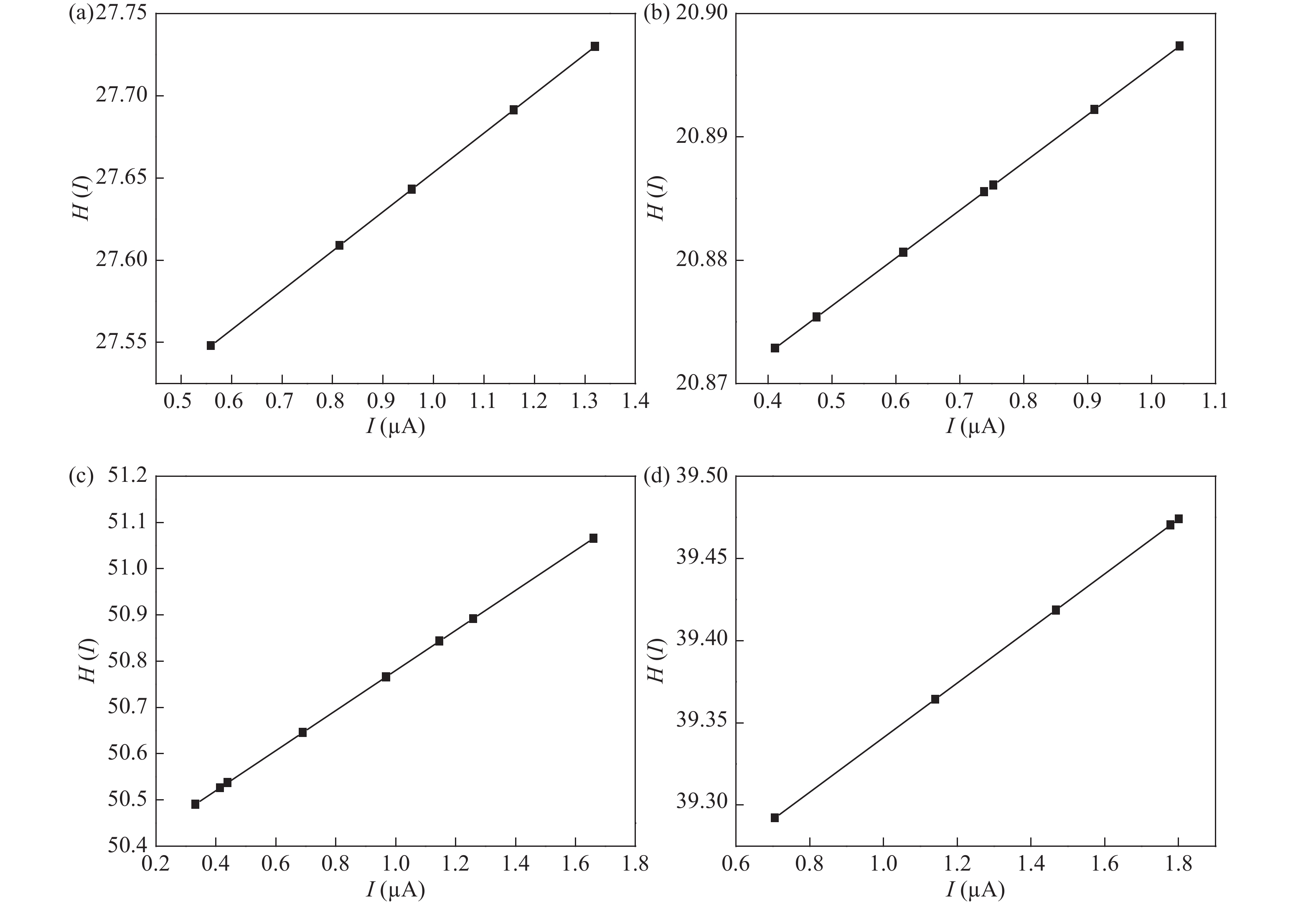
The influence of single walled carbon nanotube (SWCNT) on the series resistance (Rs) of Rose Bengal (RB) and Methyl Red (MR) dye-based organic diodes has been studied. It has been revealed from experimental results that SWCNT has a significant effect on Rs. The values of Rs are measured from current–voltage (I–V) characteristics and also by utilizing the Cheung method. Obtained values from the Cheung method have been verified using H(I)–I plots for all dye-based devices. The extracted values using these two processes show a good consistency with each other. It is observed that Rs is reduced significantly by incorporating SWCNT for both dyes. The estimated amounts of reduction of Rs using SWCNT are 76.08% and 64.23% obtained from the I–V relationship whereas the value of Rs shows a reduction of 83.5% and 67.1% when measured by using the Cheung method for RB and MR dyes respectively. The ideality factor and barrier height of the diodes have also been extracted. The ideality factor has decreased with incorporation of SWCNT. A reduction in barrier height for the devices has also been observed in the presence of SWCNT.
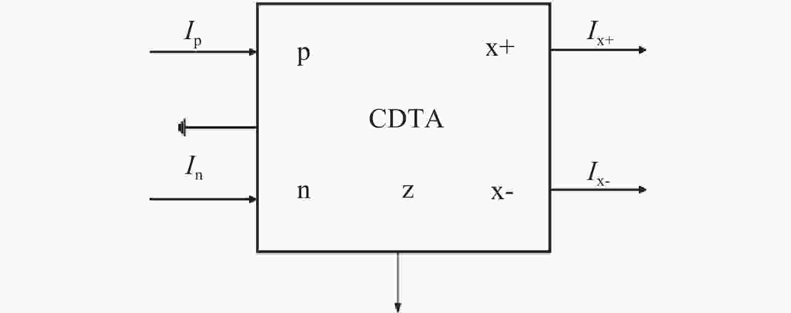
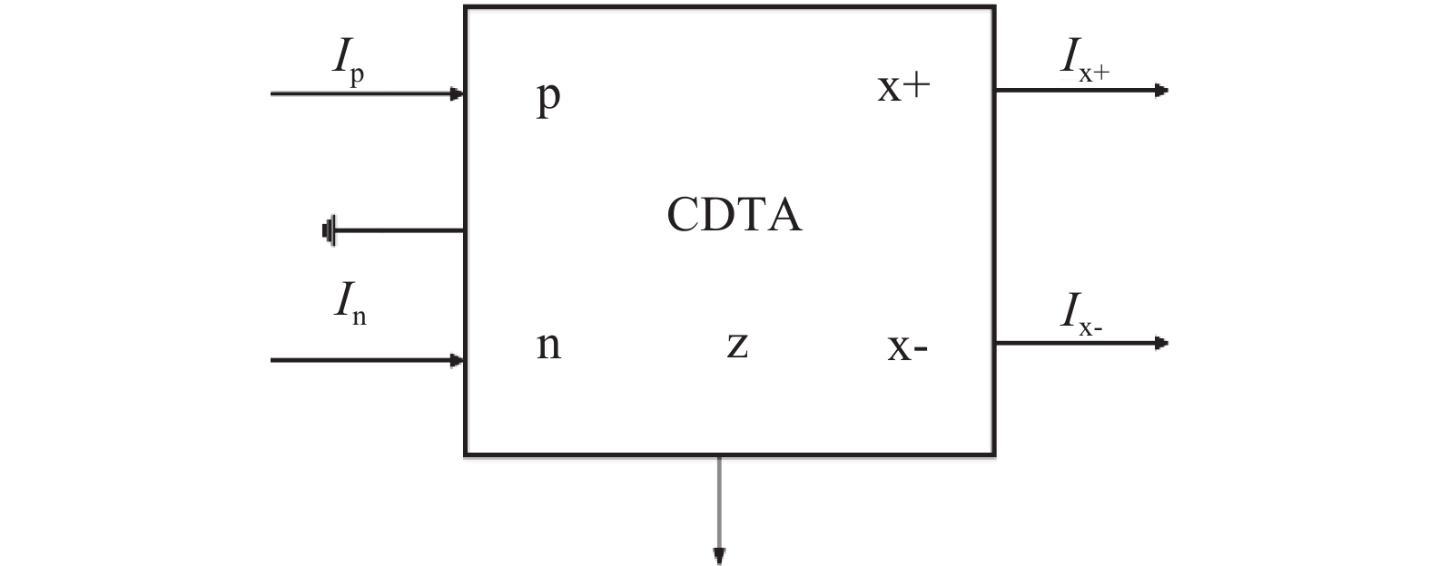
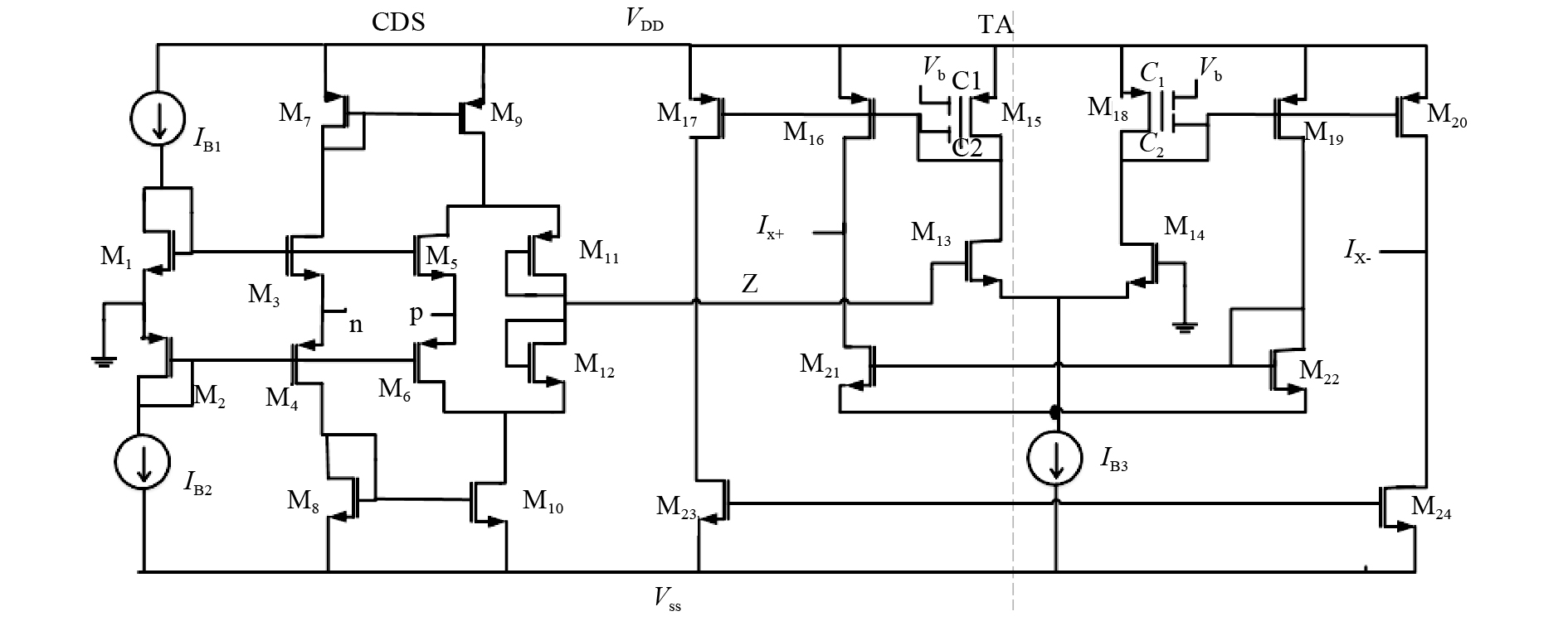
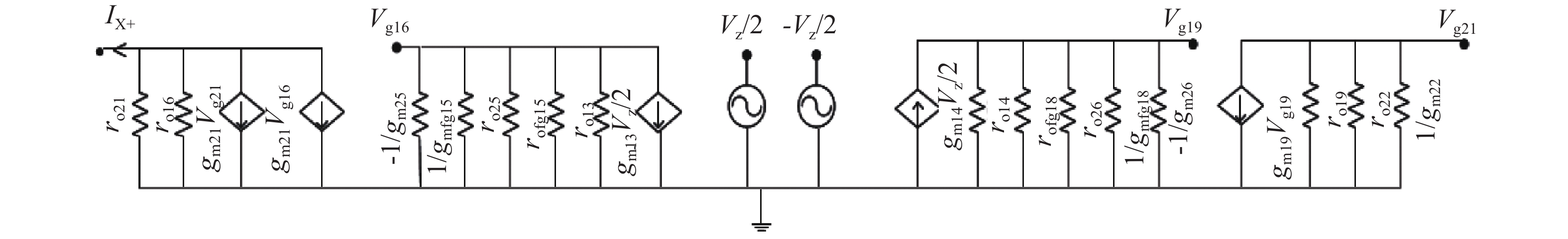
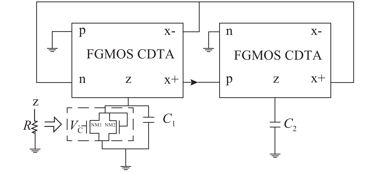
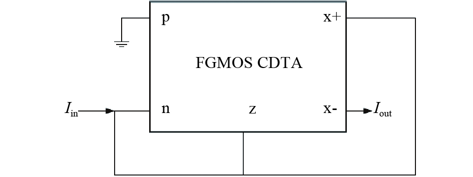
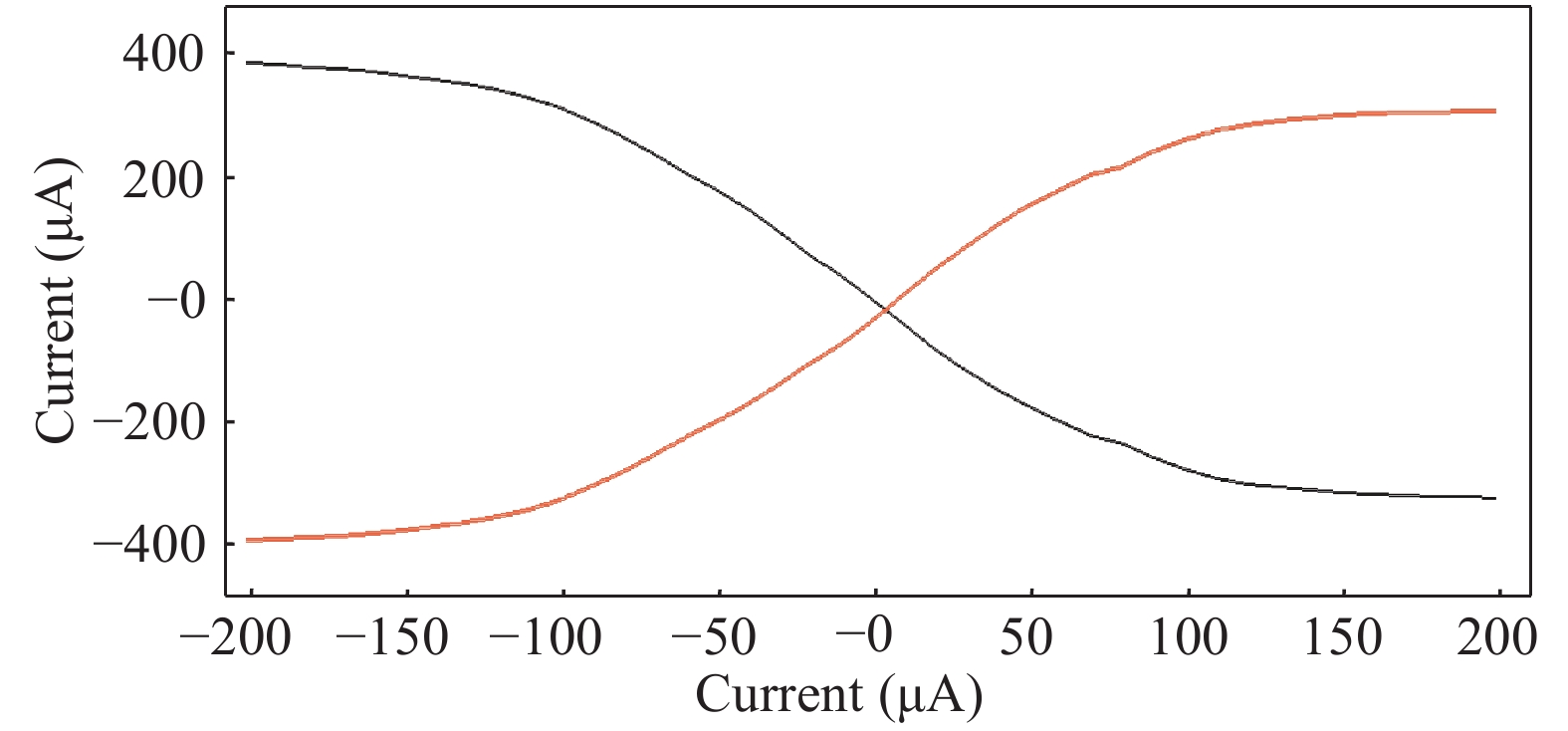
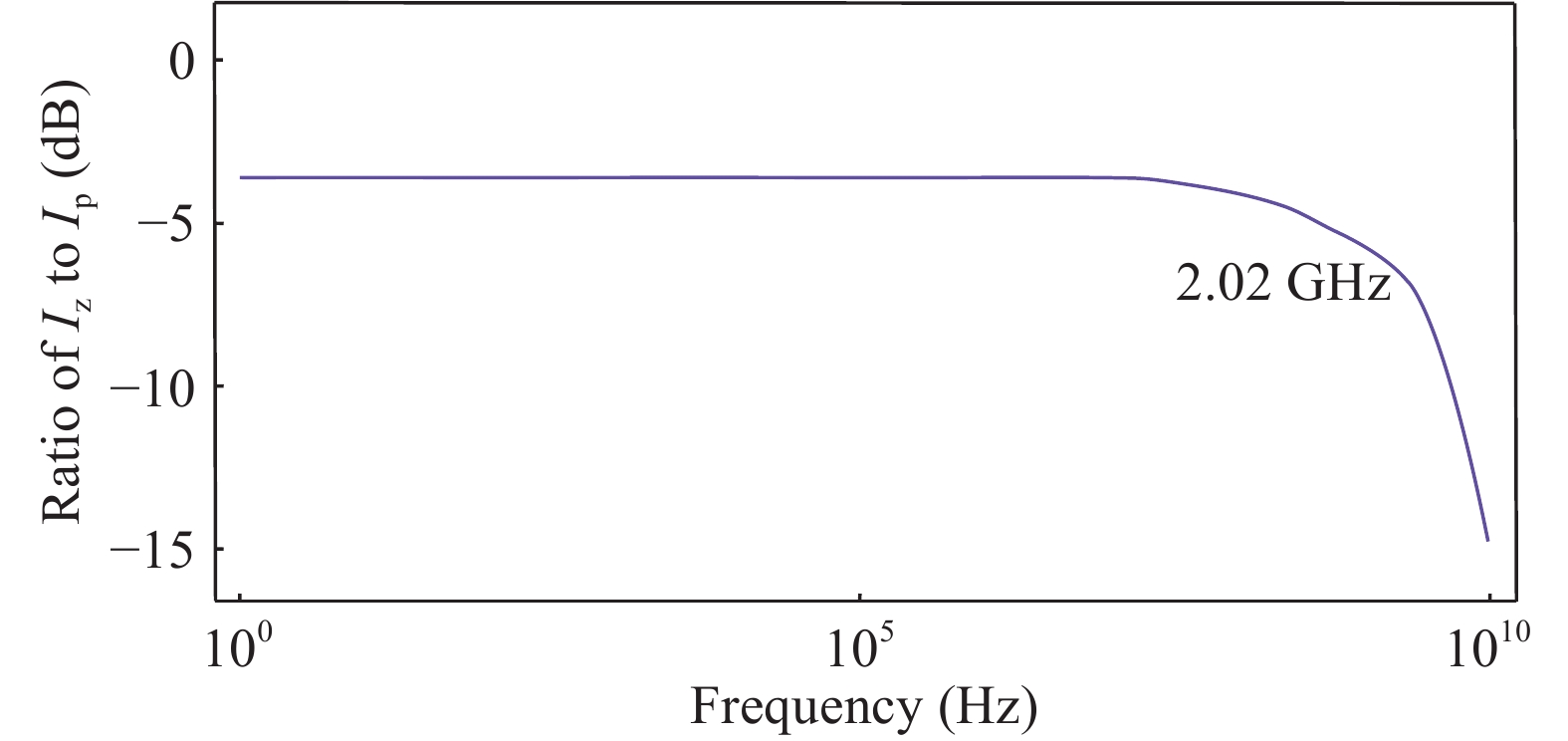
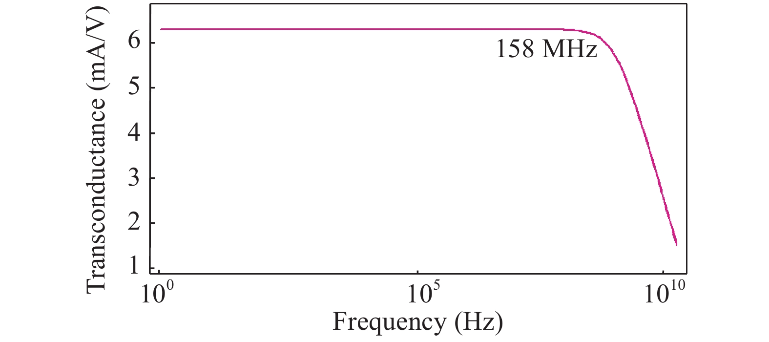
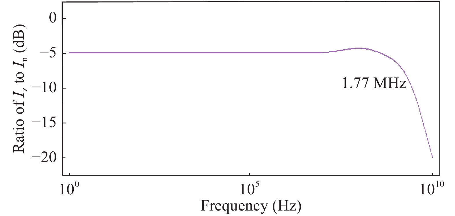
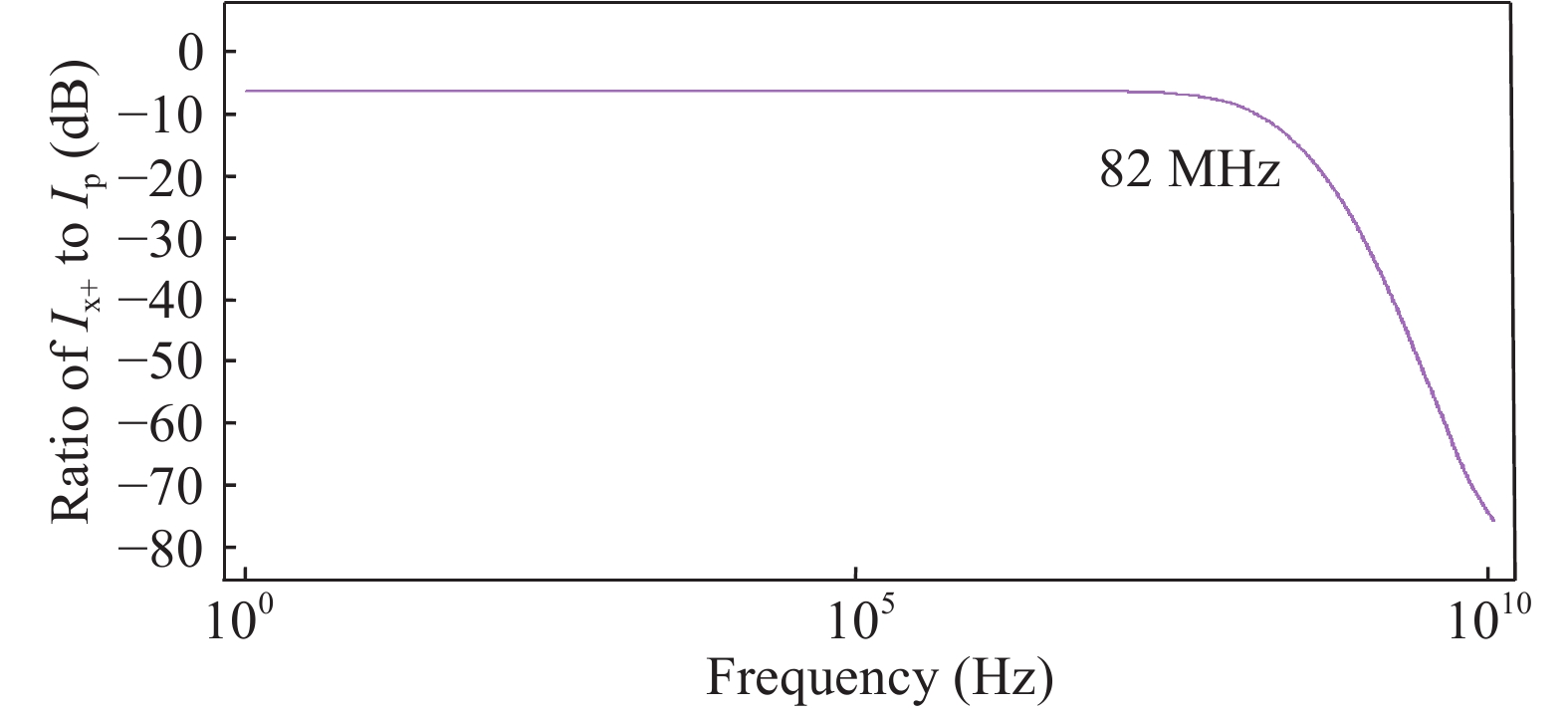
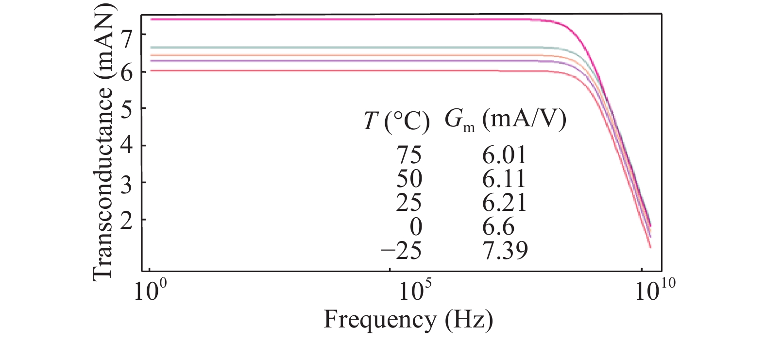
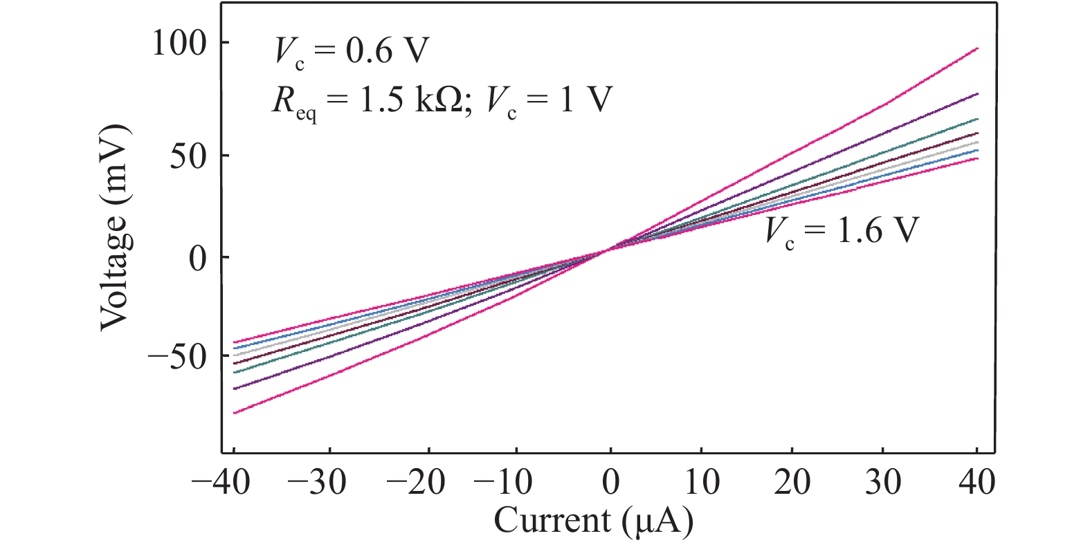
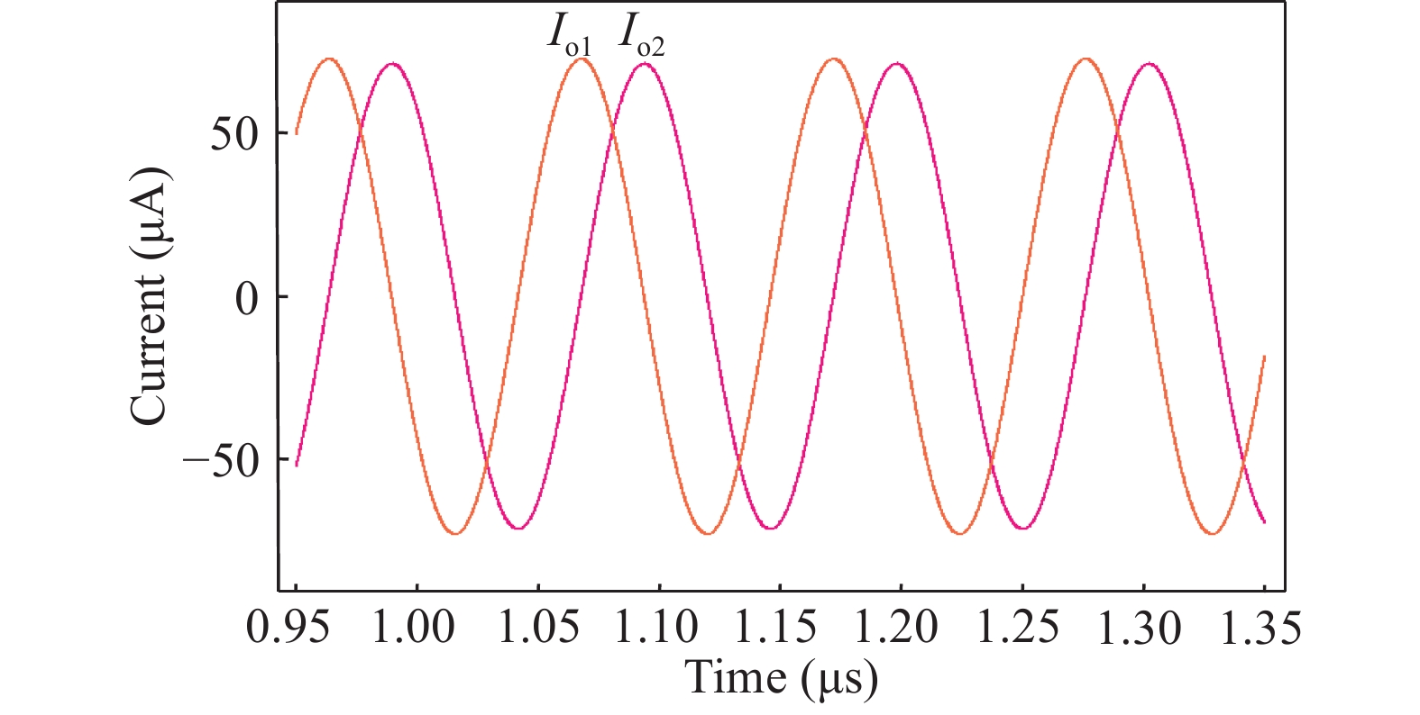
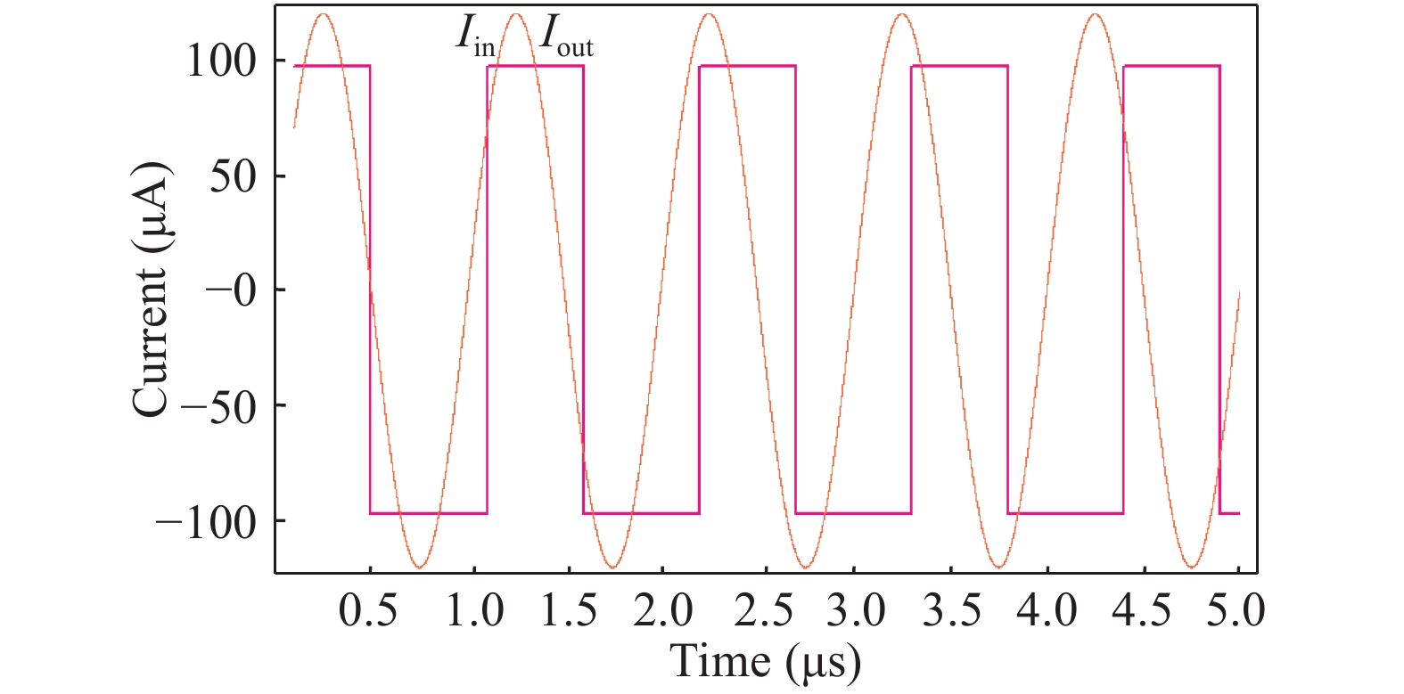
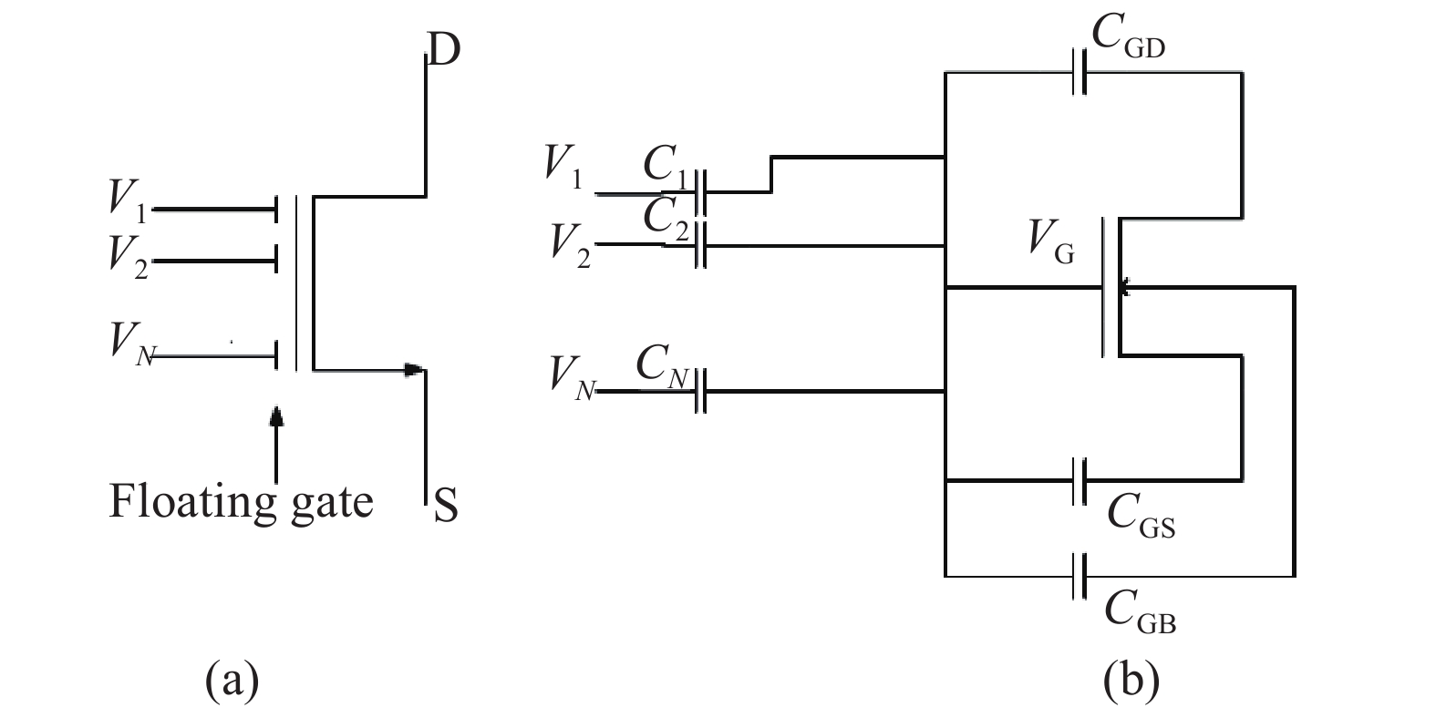
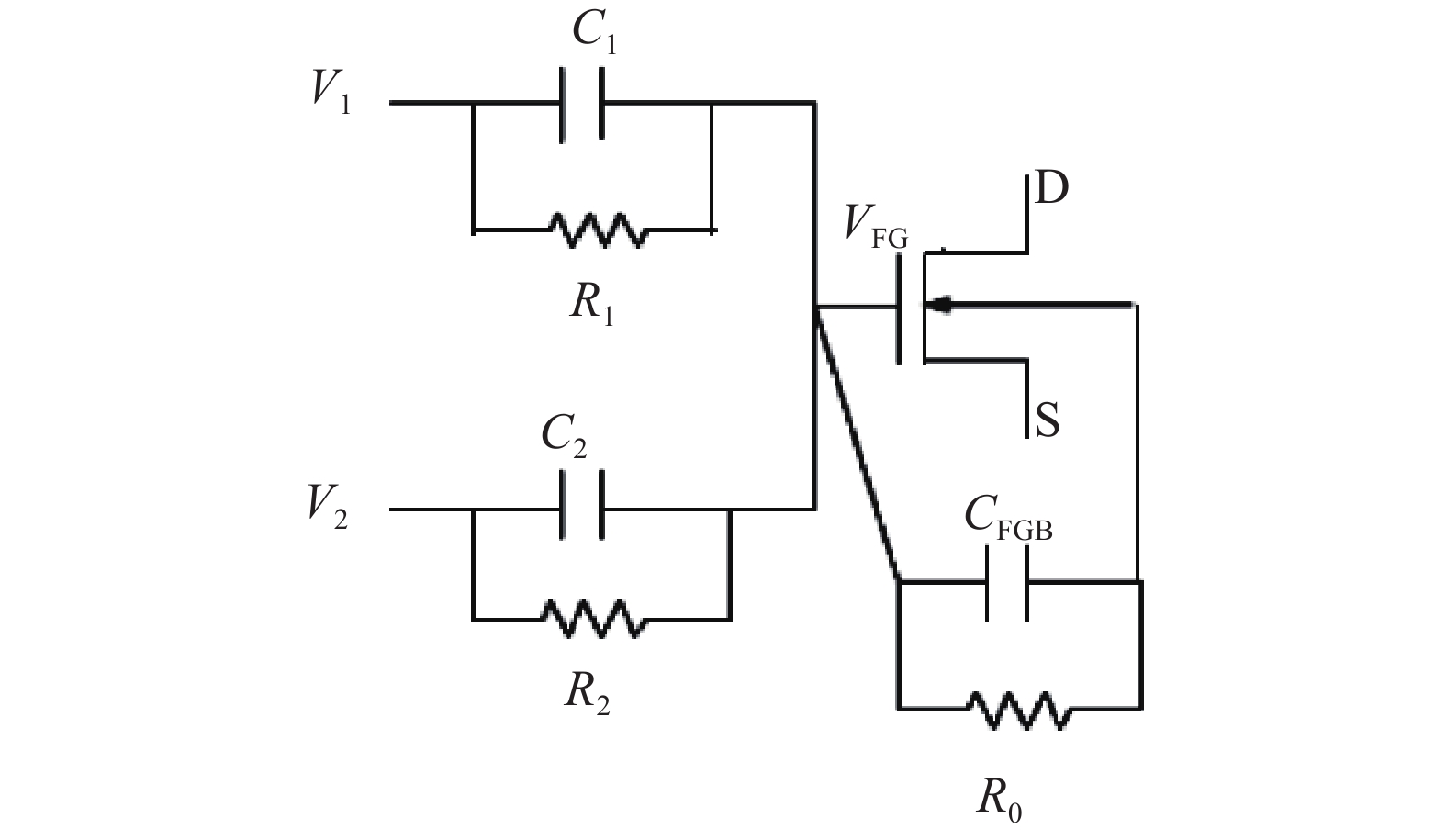
This article presents a low voltage low power configuration of current differencing transconductance amplifier (CDTA) based on floating gate MOSFET. The proposed CDTA variant operates at lower supply voltage ±1.4 V with total static power dissipation of 2.60 mW due to the low voltage feature of floating gate MOSFET. High transconductance up to 6.21 mA/V is achieved with extended linear range of the circuit i.e. ±130 μA. Two applications are illustrated to demonstrate the effectiveness of the proposed active block. A quadrature oscillator is realized using FGMOS based CDTA, two capacitors, and a resistor. The resistor is implemented using two NMOSFETs to provide high linearity and tunablility. Another application is the Schmitt trigger circuit based on the proposed CDTA variant. All circuits are simulated by using SPICE and TSMC 130 nm technology.

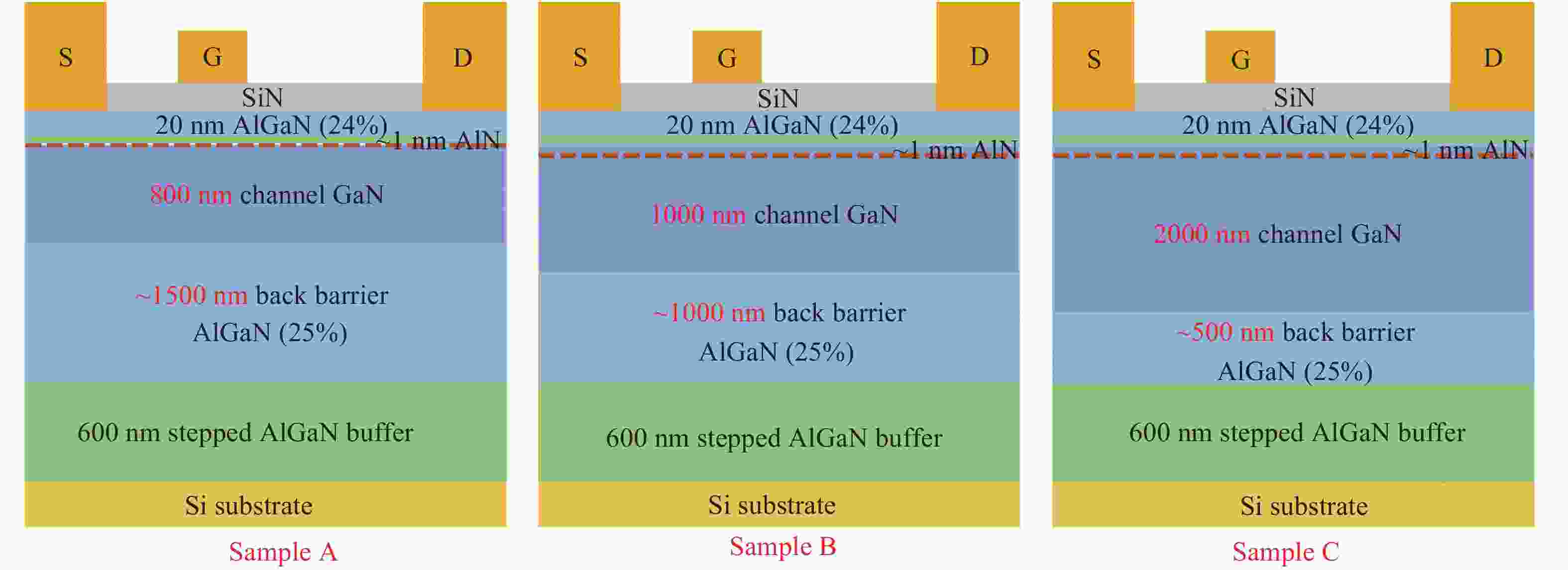
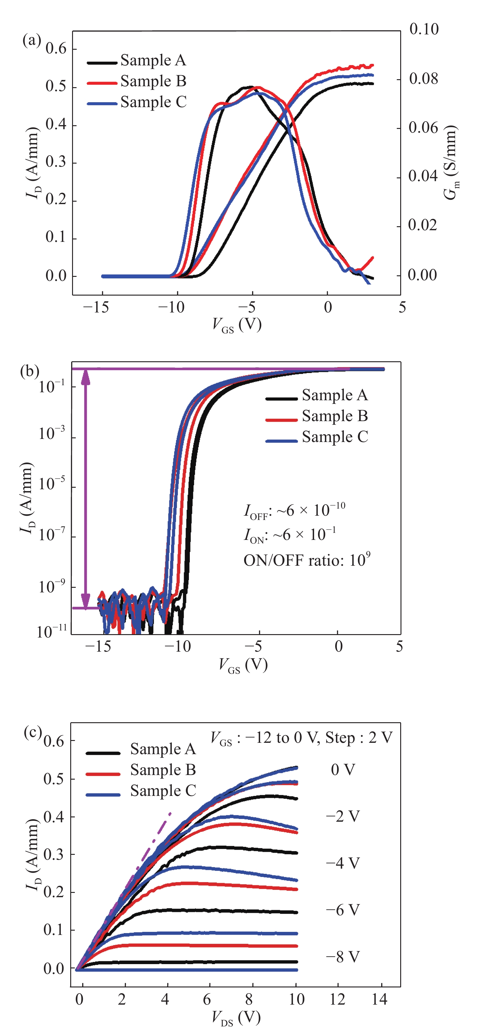
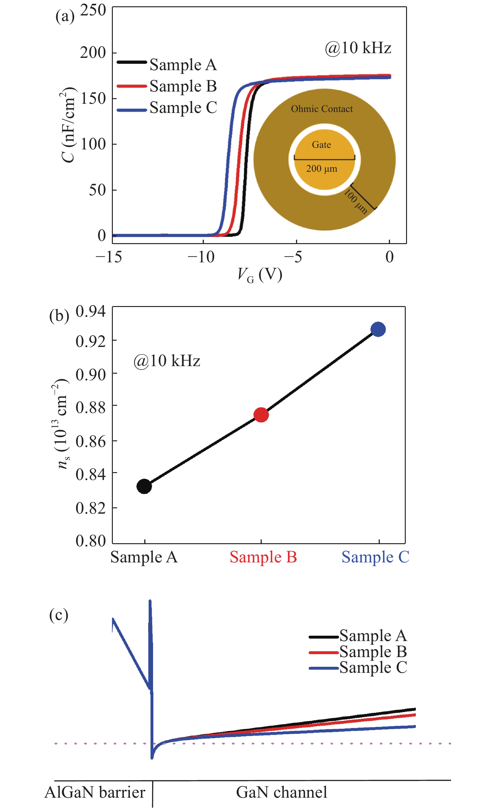
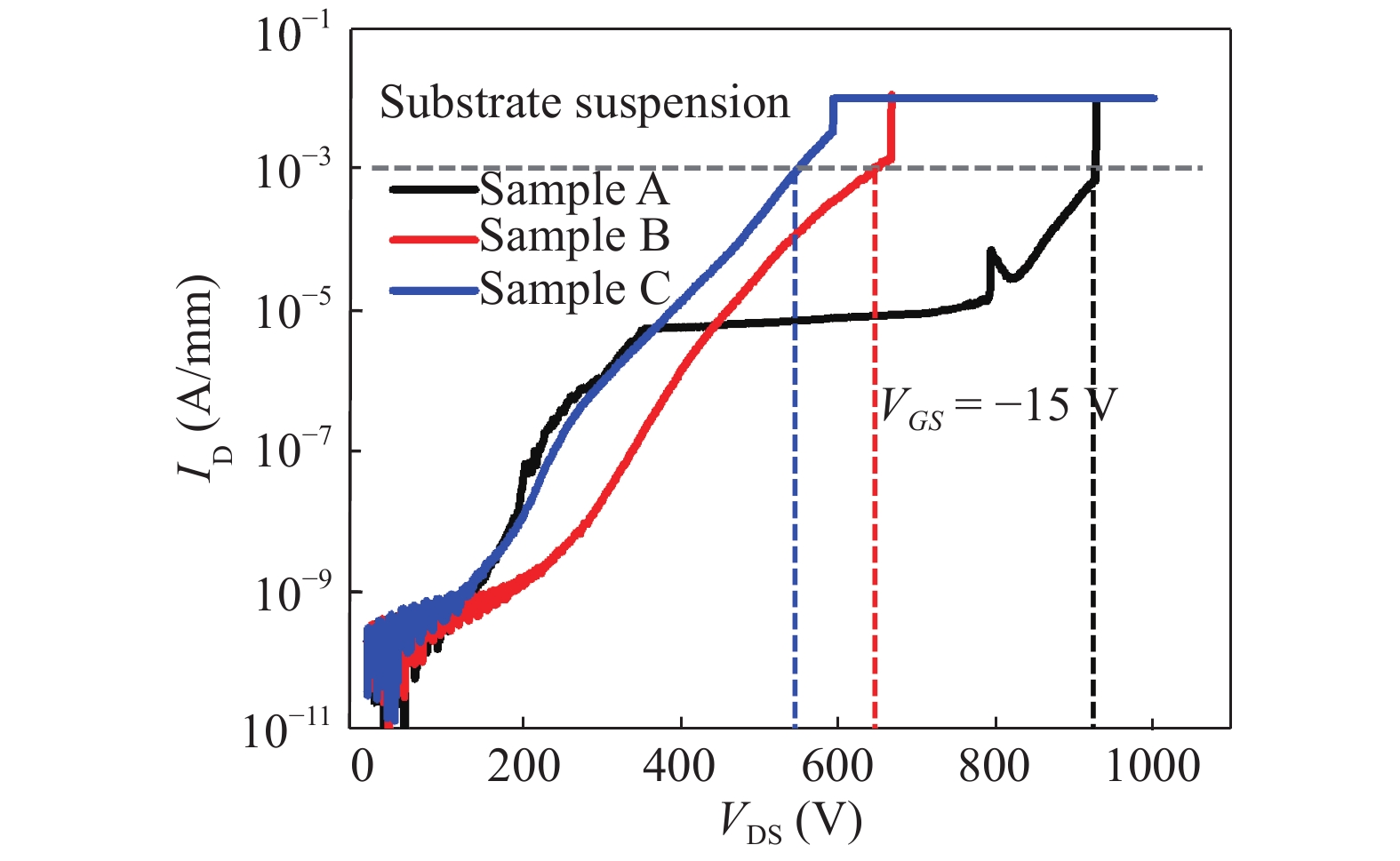
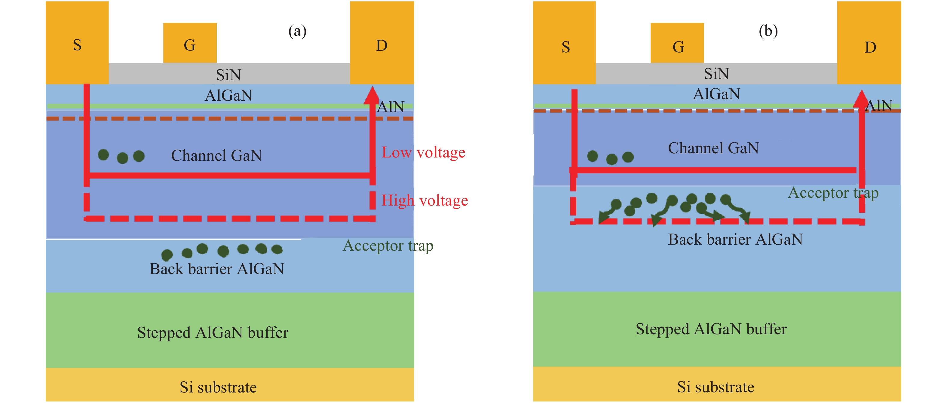
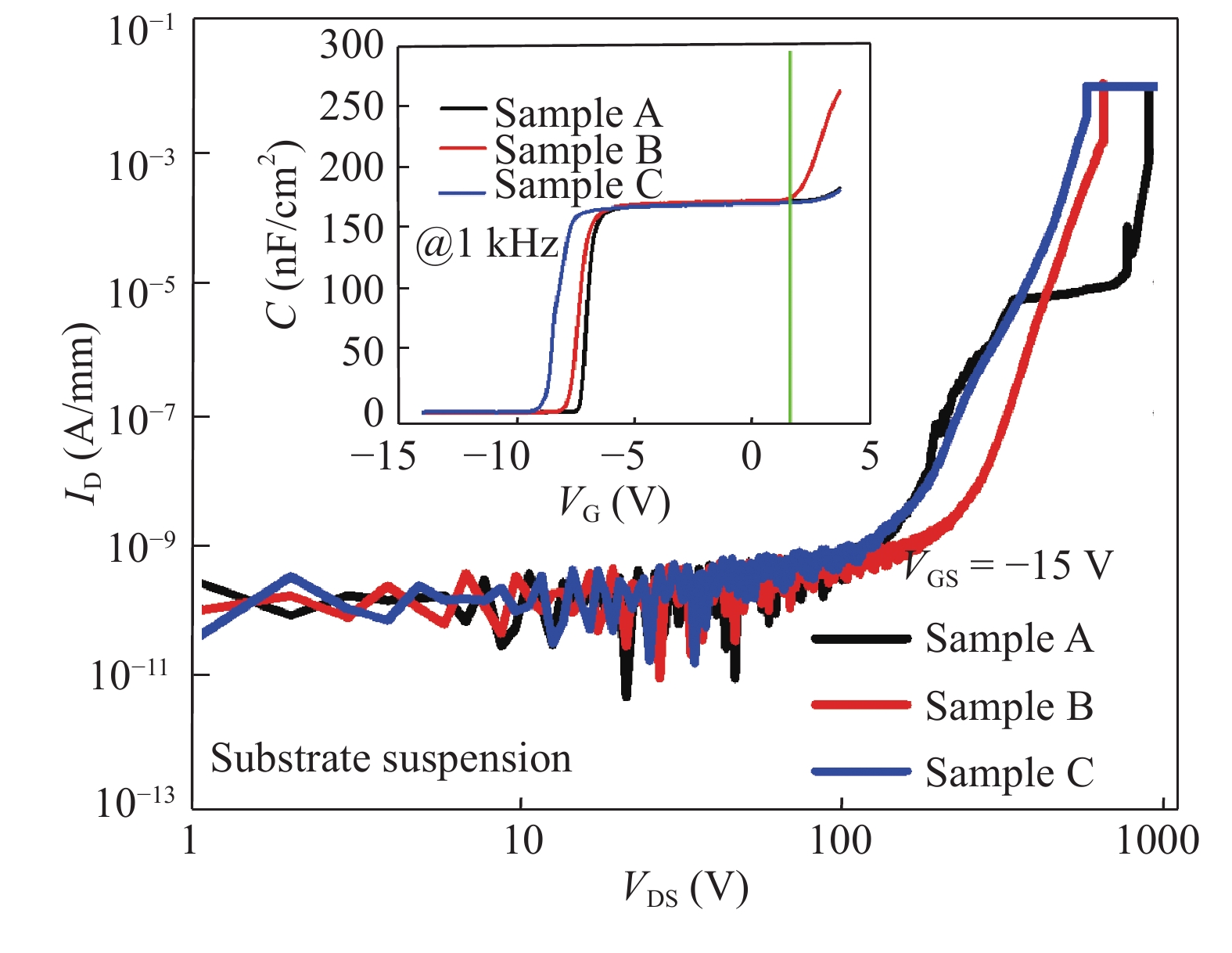
The leakage current and breakdown voltage of AlGaN/GaN/AlGaN high electron mobility transistors on silicon with different GaN channel thicknesses were investigated. The results showed that a thin GaN channel was beneficial for obtaining a high breakdown voltage, based on the leakage current path and the acceptor traps in the AlGaN back-barrier. The breakdown voltage of the device with an 800 nm-thick GaN channel was 926 V @ 1 mA/mm, and the leakage current increased slowly between 300 and 800 V. Besides, the raising conduction band edge of the GaN channel by the AlGaN back-barrier lead to little degradation for sheet 2-D electron gas density, especially, in the thin GaN channel. The transfer and output characteristics were not obviously deteriorated for the samples with different GaN channel thickness. Through optimizing the GaN channel thickness and designing the AlGaN back-barrier, the lower leakage current and higher breakdown voltage would be possible.

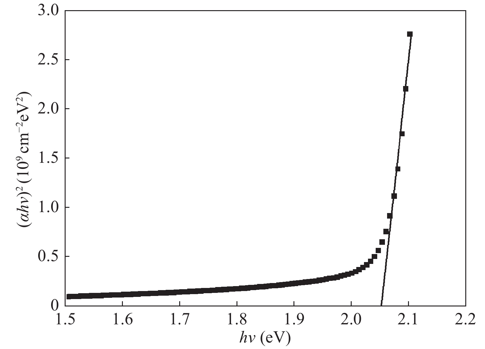
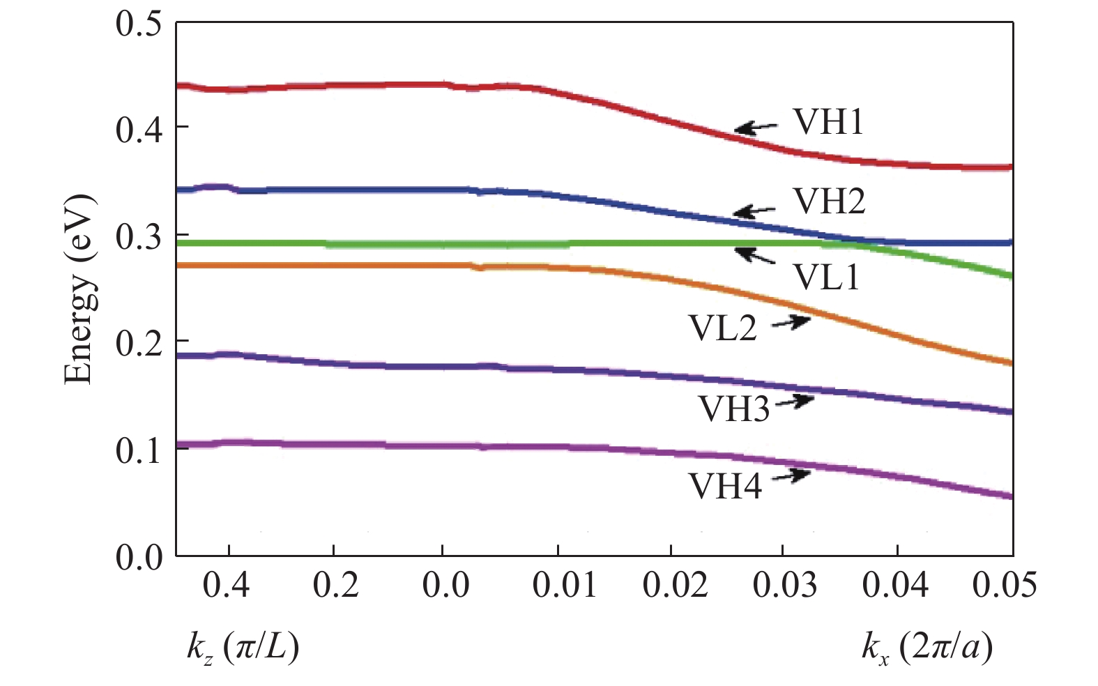
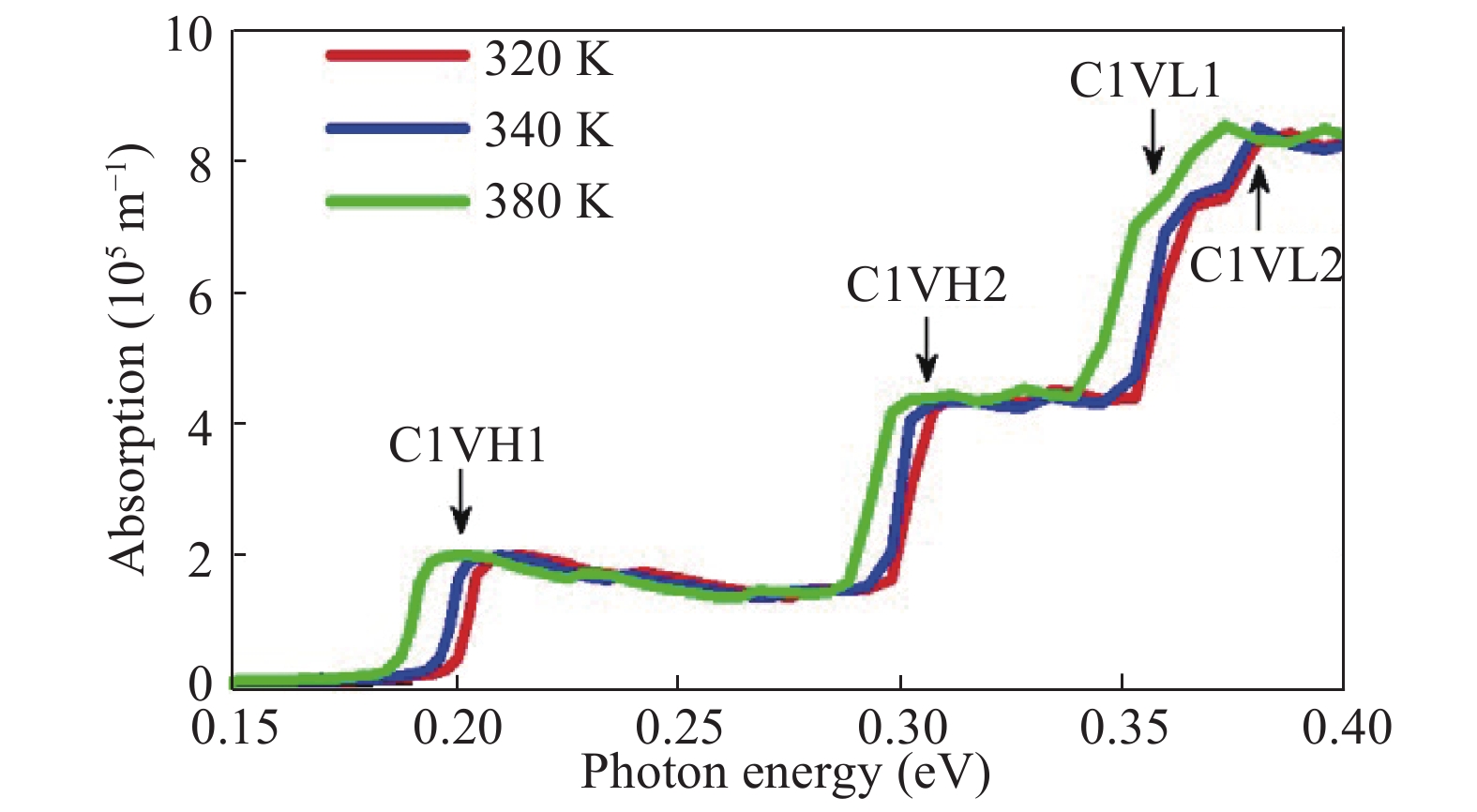
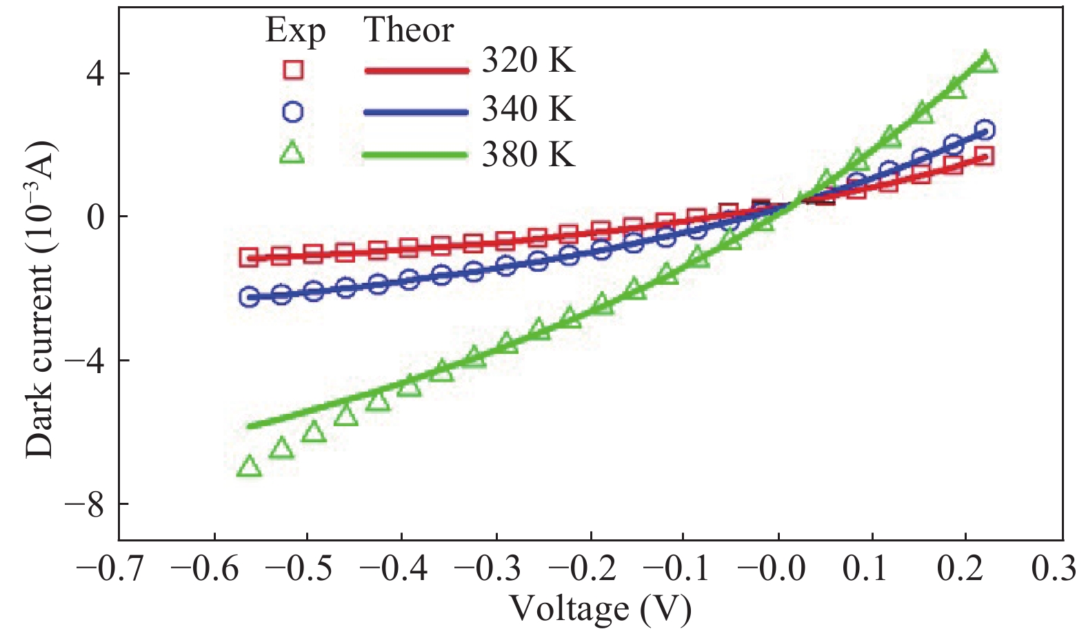
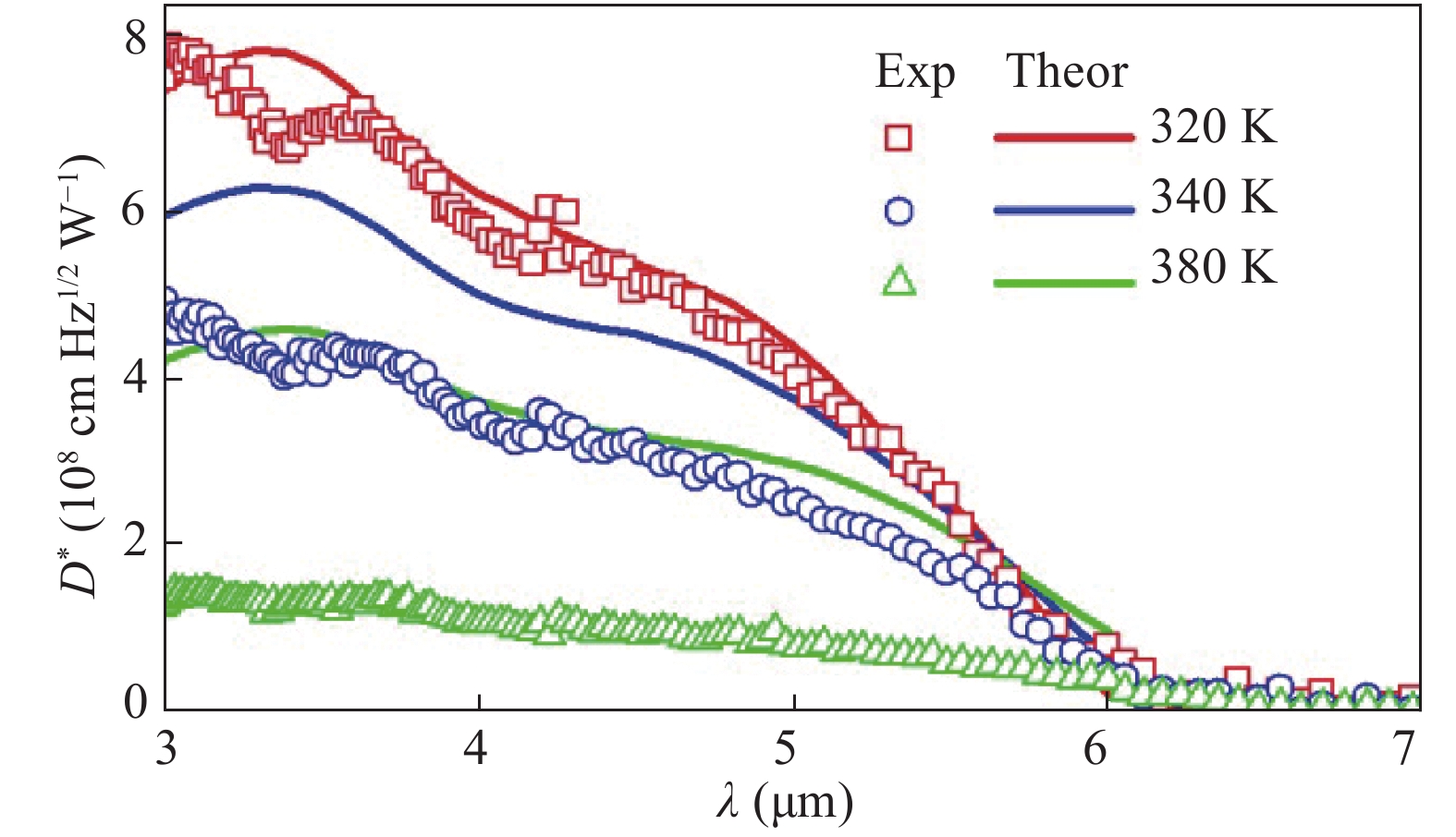
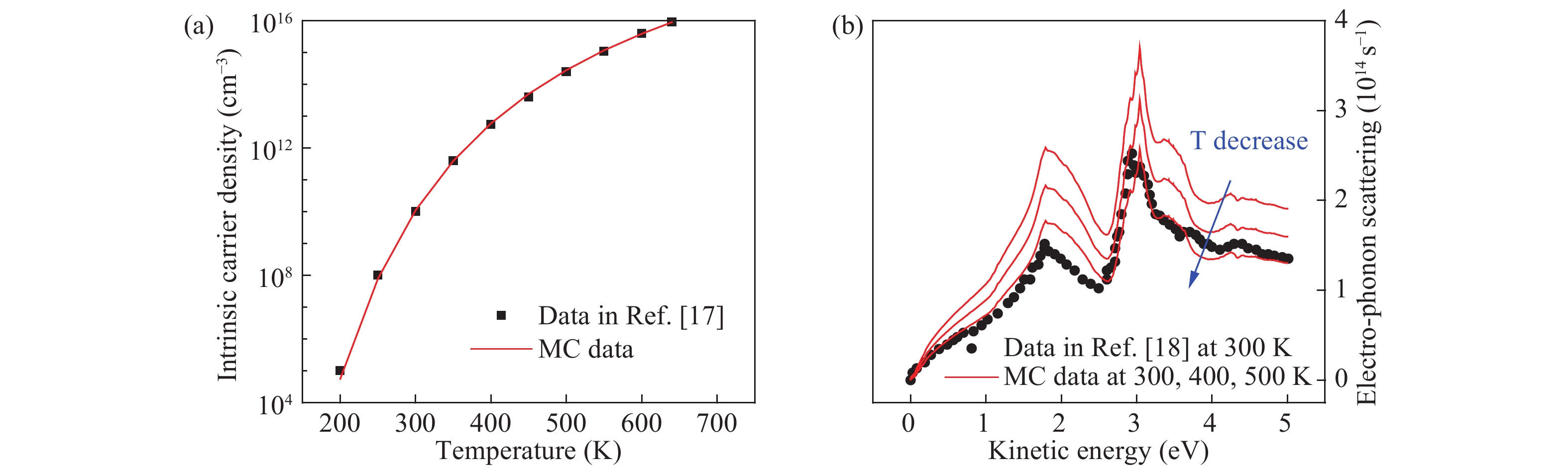
The investigation of the interband type-II superlattice InAs/GaSb cascade photodetector in the temperature range of 320–380 K is presented. The article is devoted to the theoretical modeling of the cascade detector characteristics by the use of the SimuApsys platform and the 4-band model (k∙p 8 × 8 method). The obtained theoretical characteristics are comparable with experimentally measured ones, suggesting that transport in the absorber is determined by the dynamics of intrinsic carriers and by their lifetime. An overlap equal to 120 meV was used in calculations and a correction term in the " non-common atom” model Hxy = 700 meV was added to the Hamiltonian. The electron and hole effective masses from dispersion curves were estimated and absorption coefficient α was calculated. Based on the simulation detectivity, D* characteristics in the temperature range 320–380 K were calculated. The simulated theoretical characteristics at 320 K are comparable to experimentally measured ones, however at higher temperatures, the experimental value of D* does not reach the theoretical values due to the low resistance of the device and short diffusion length.

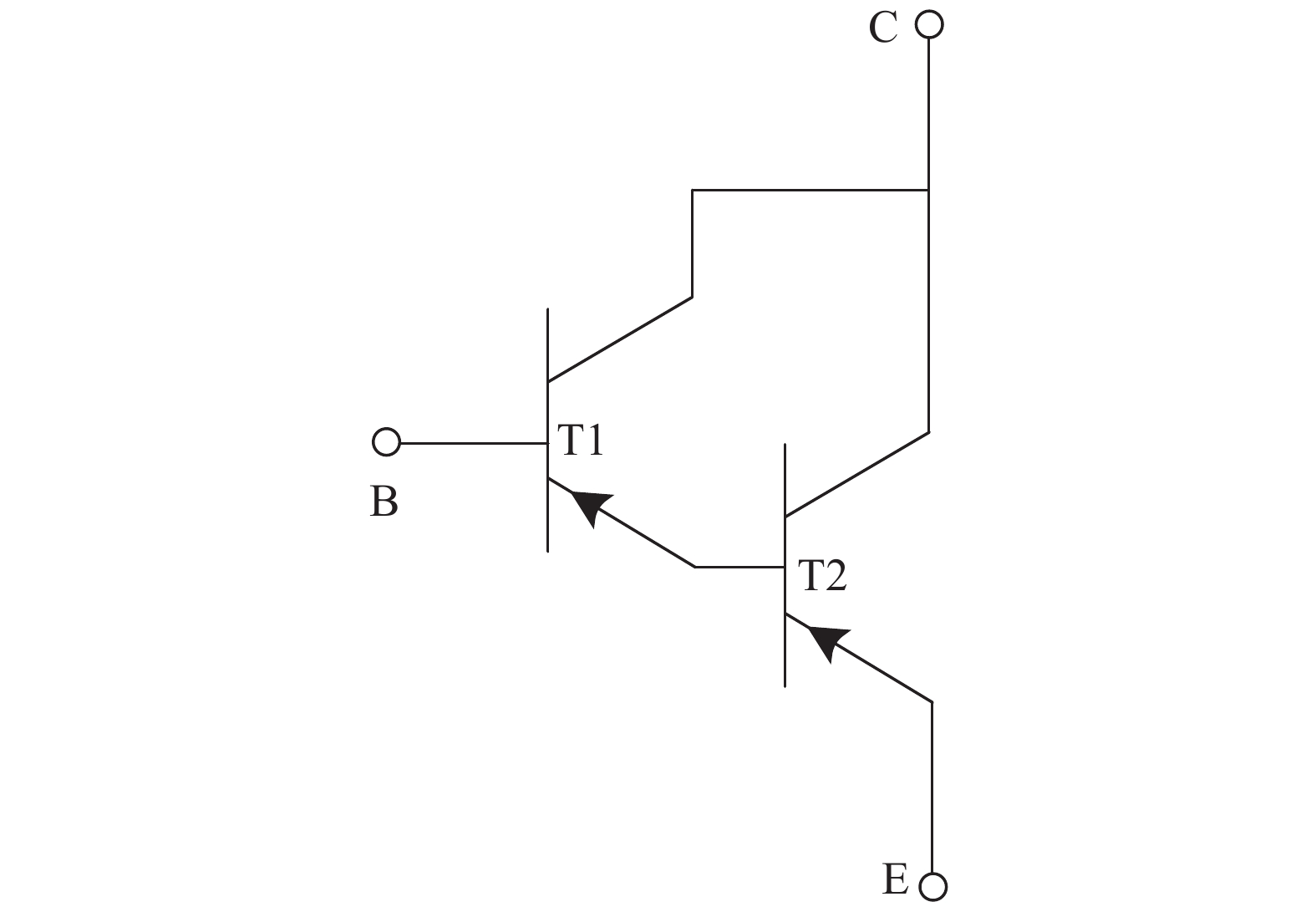
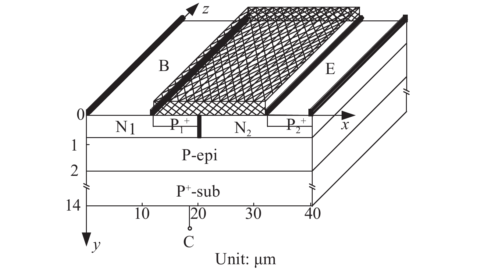
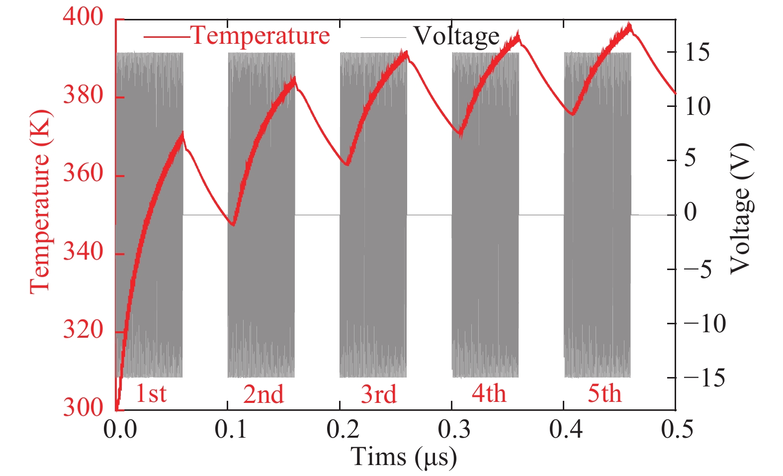
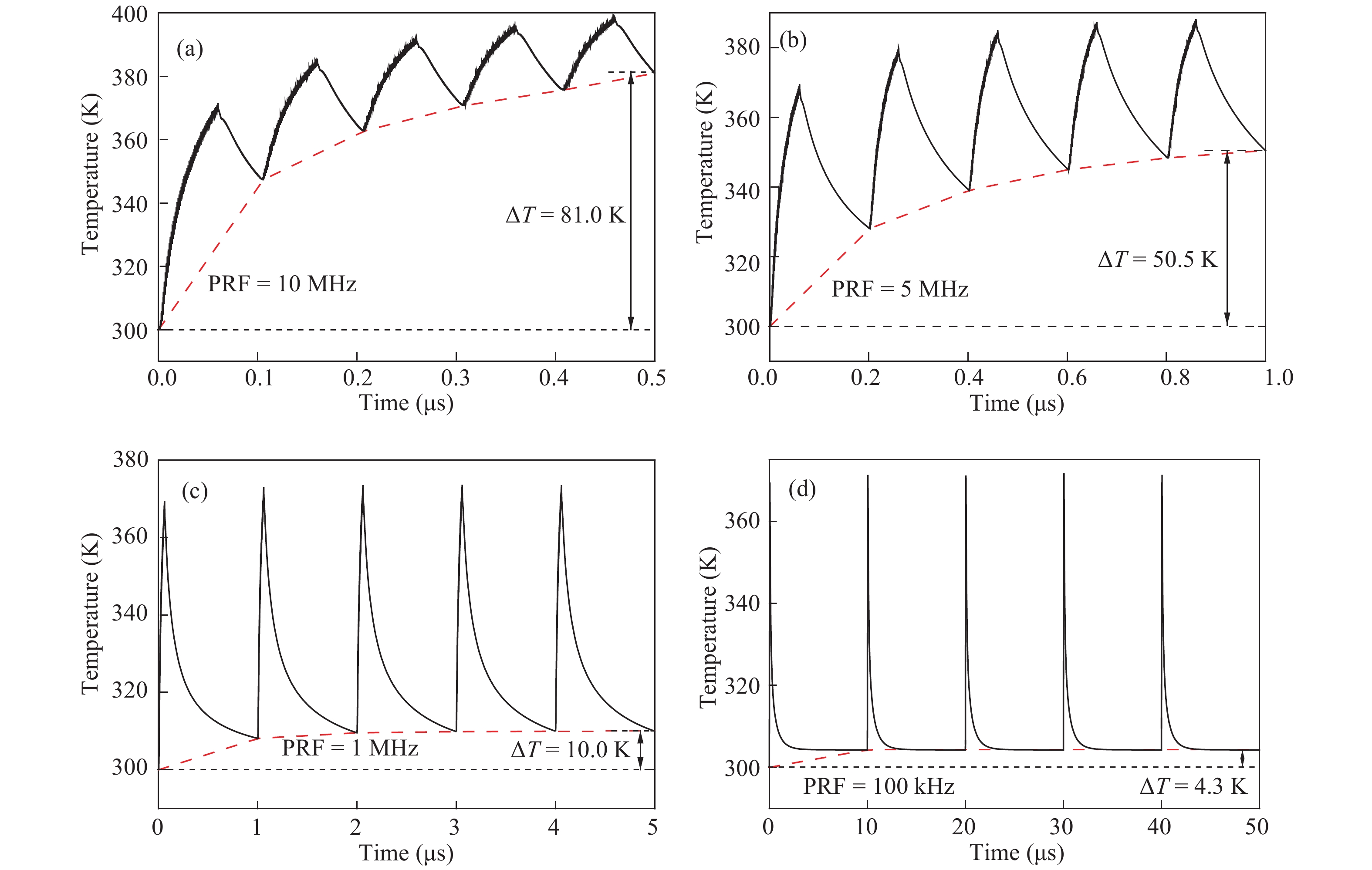
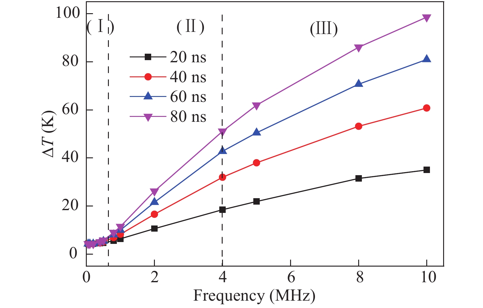
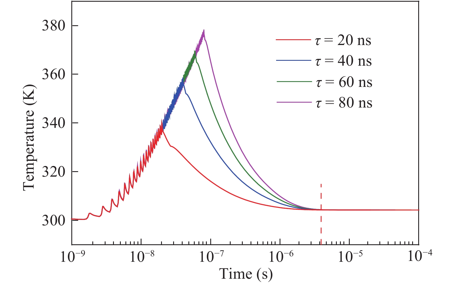
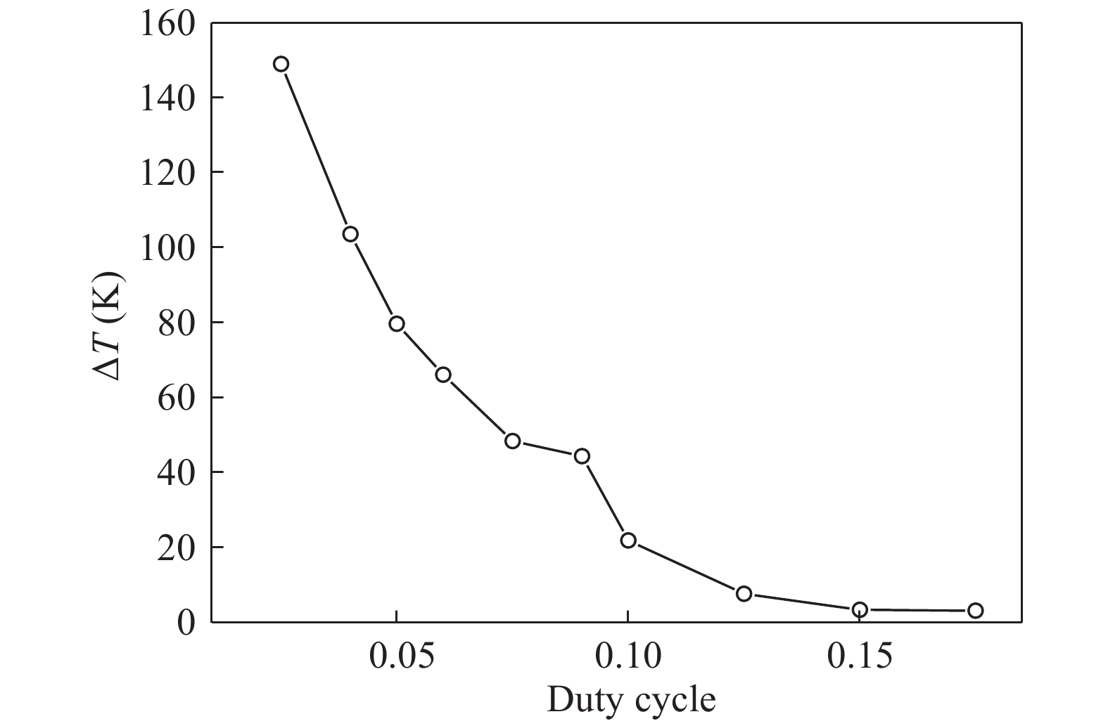
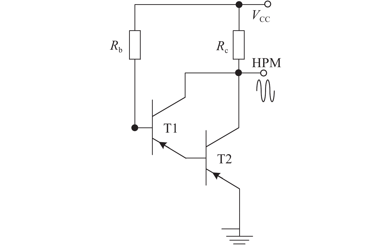
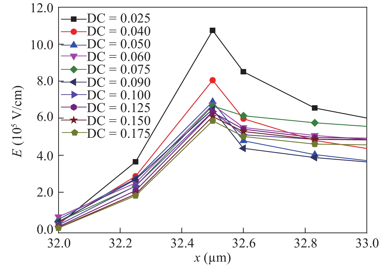
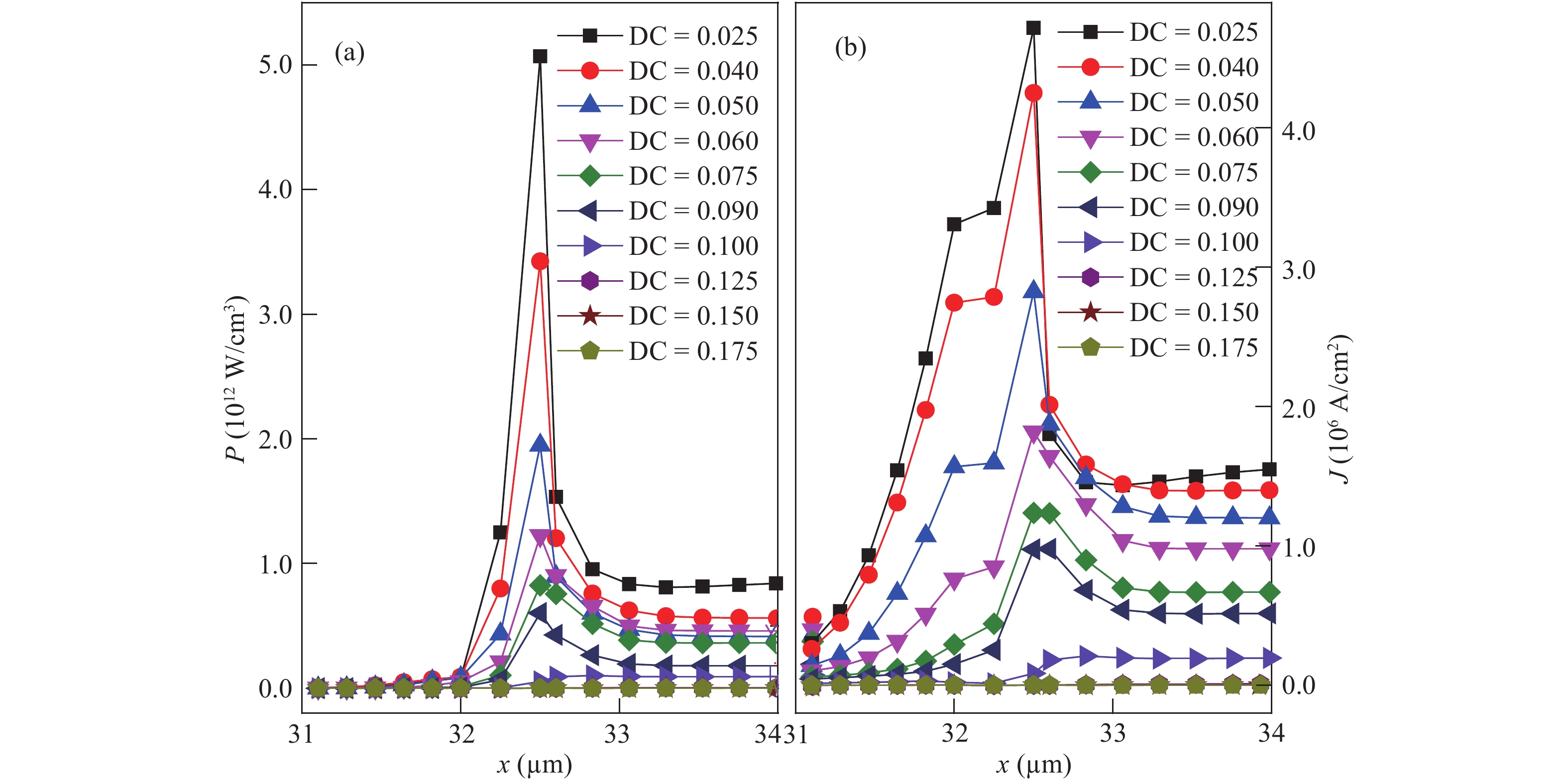
Theoretical research on the heat accumulation effect of a Darlington transistor induced by high power microwave is conducted, and temperature variation as functions of pulse repetitive frequency (PRF) and duty cycle (DC) are studied. According to the distribution of the electronic field and the current density in the Darlington transistor, the research of the damage mechanism is carried out. The results show that for repetitive pulses with the same pulse widths and different PRFs, the value of temperature variation increases with PRF increases, and the peak temperature has almost no change when PRF is lower than 200 kHz; while for the repetitive pulses with the same PRF and different pulse widths, the larger the pulse width is, the greater temperature variation varies. The response of the peak temperature caused by a single pulse demonstrates that there is no temperature variation when the rising time is much shorter than the falling time. In addition, the relationship between the temperature variation and the time during the rising edge time as well as that between the temperature variation and the time during the falling edge time are obtained utilizing the curve fitting method. Finally, for a certain average power, with DC increases the value of temperature variation decreases.
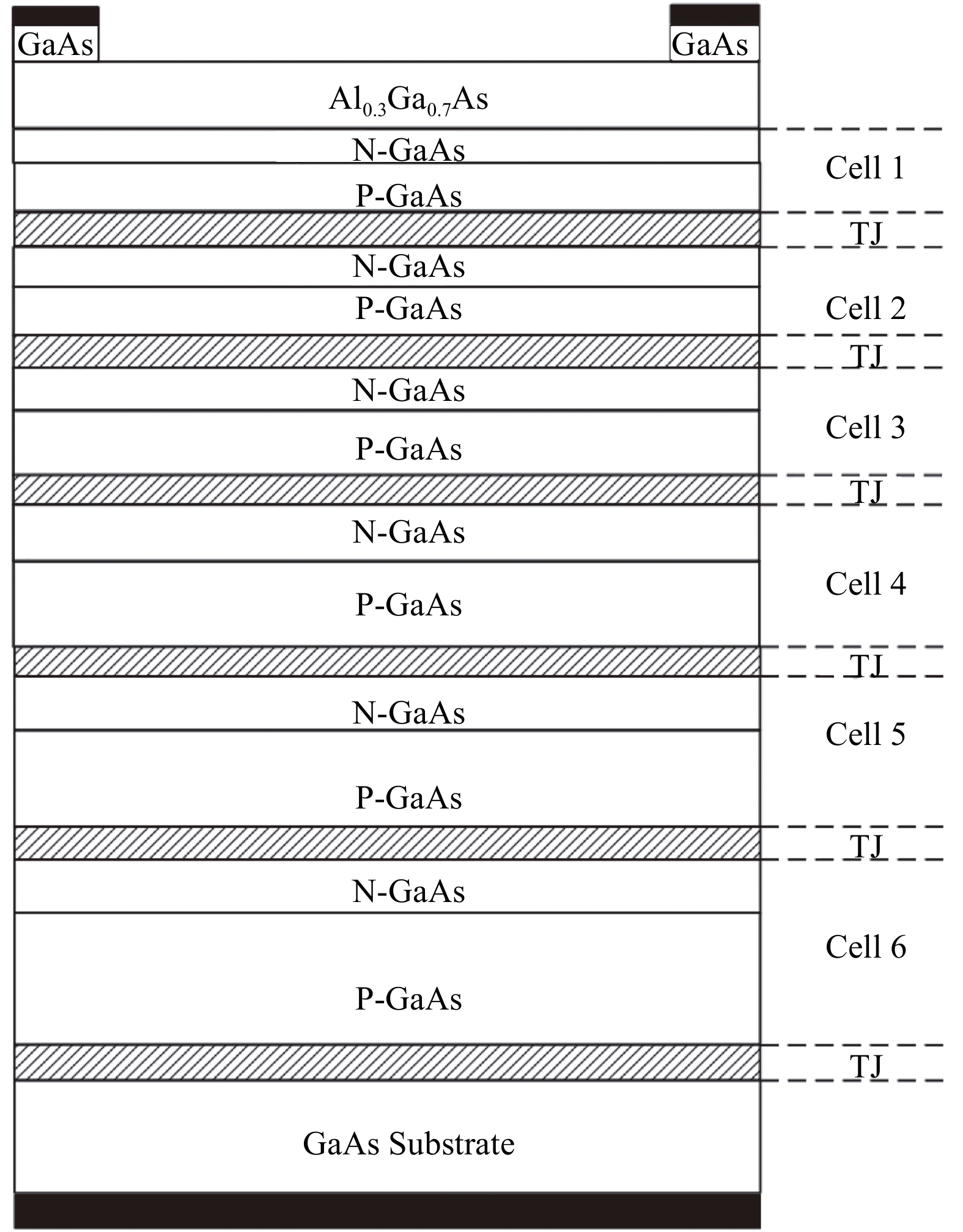
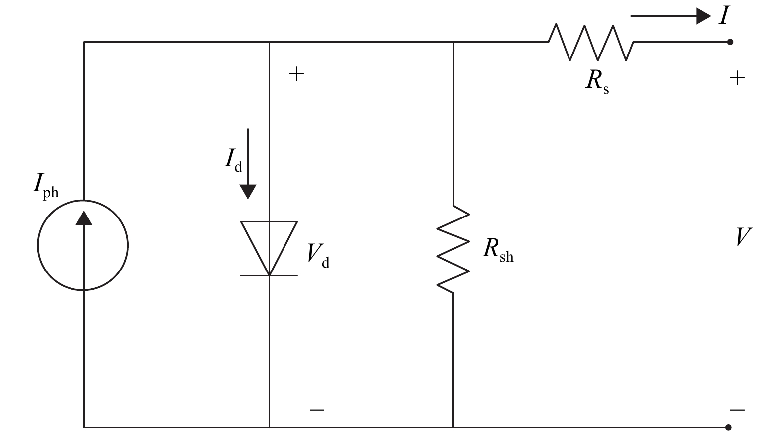
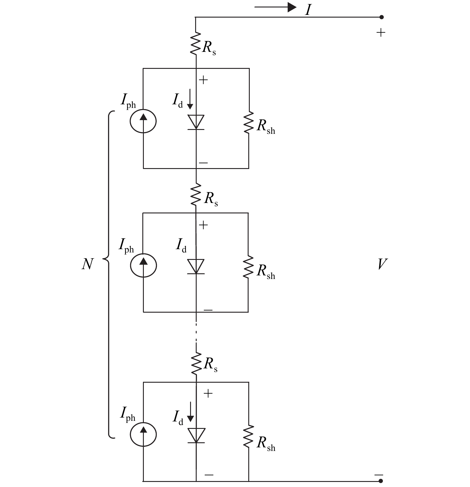
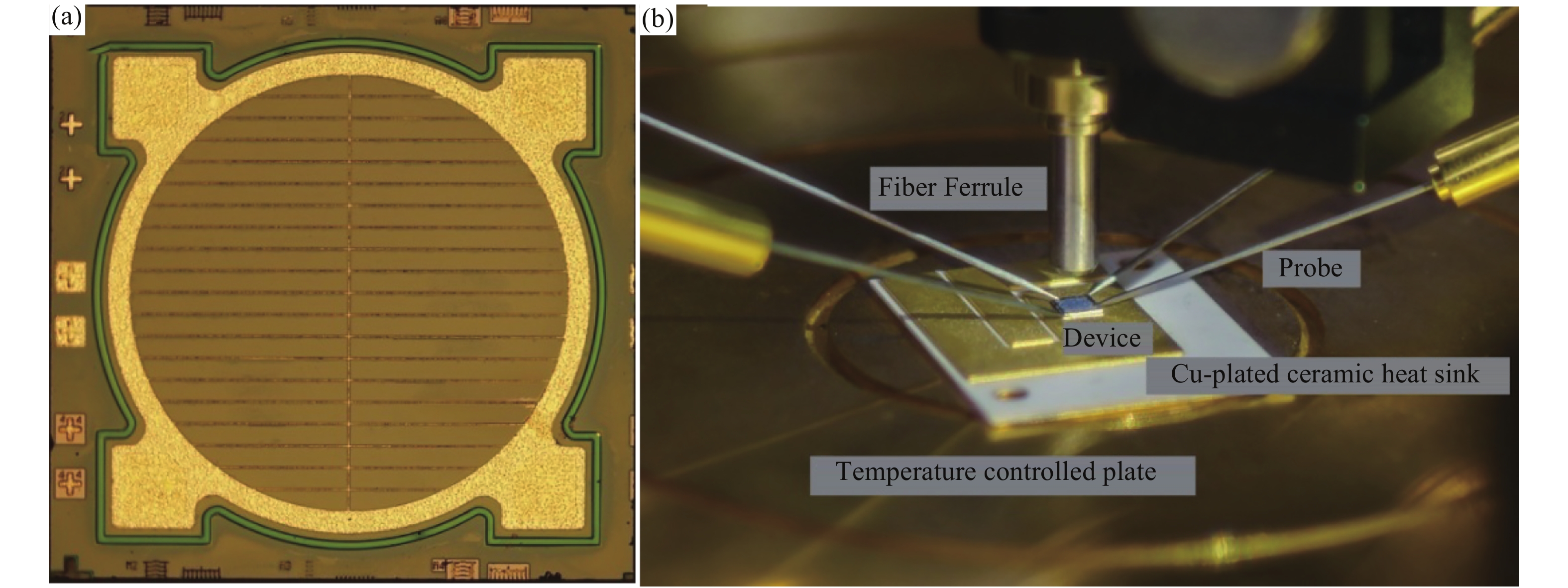
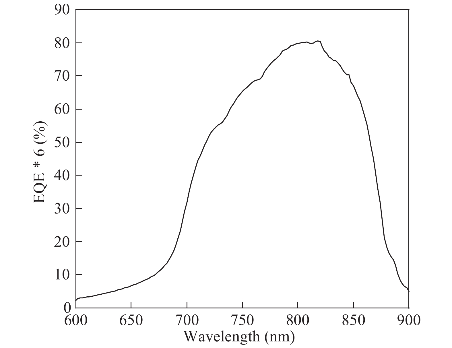
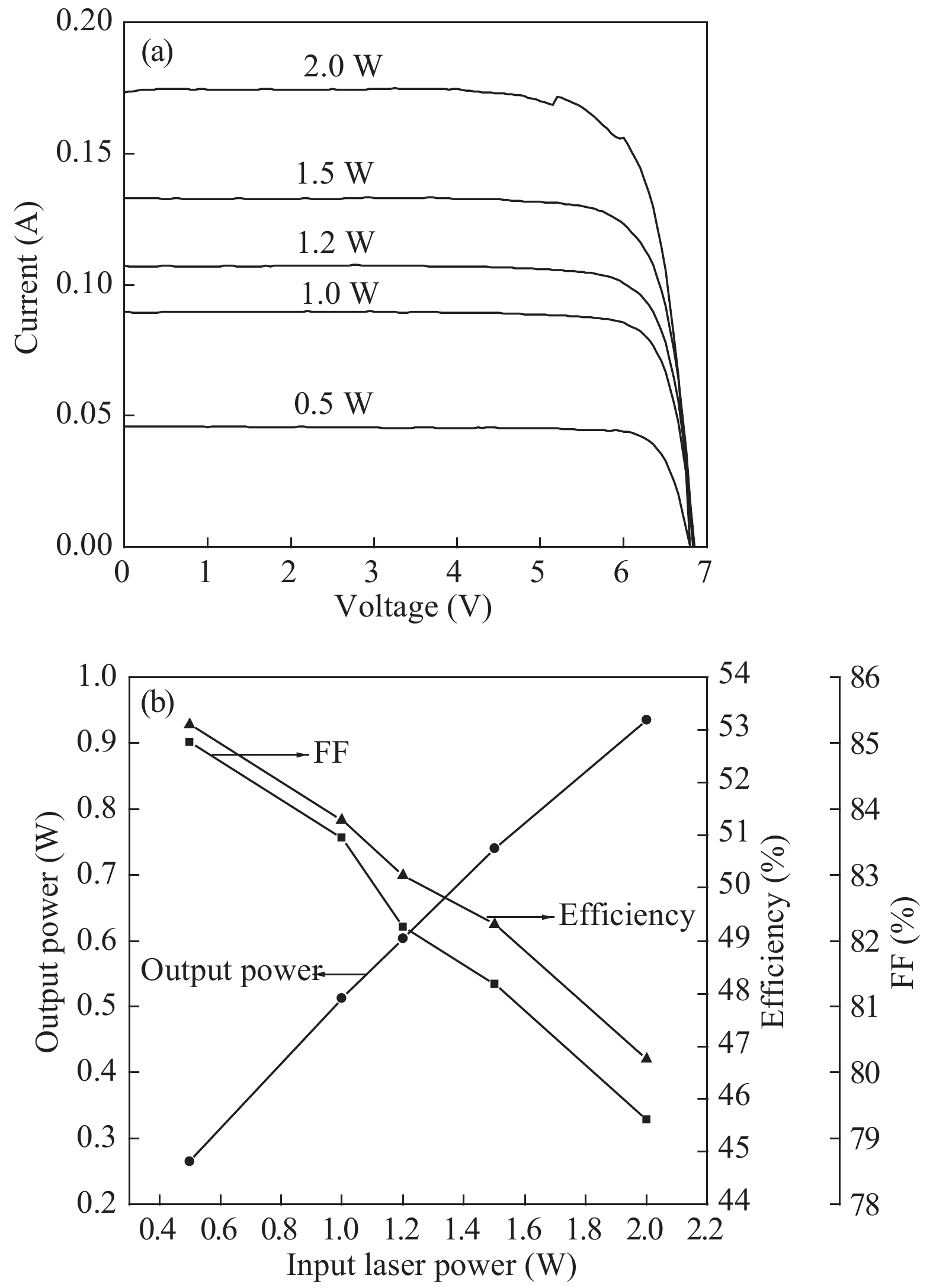
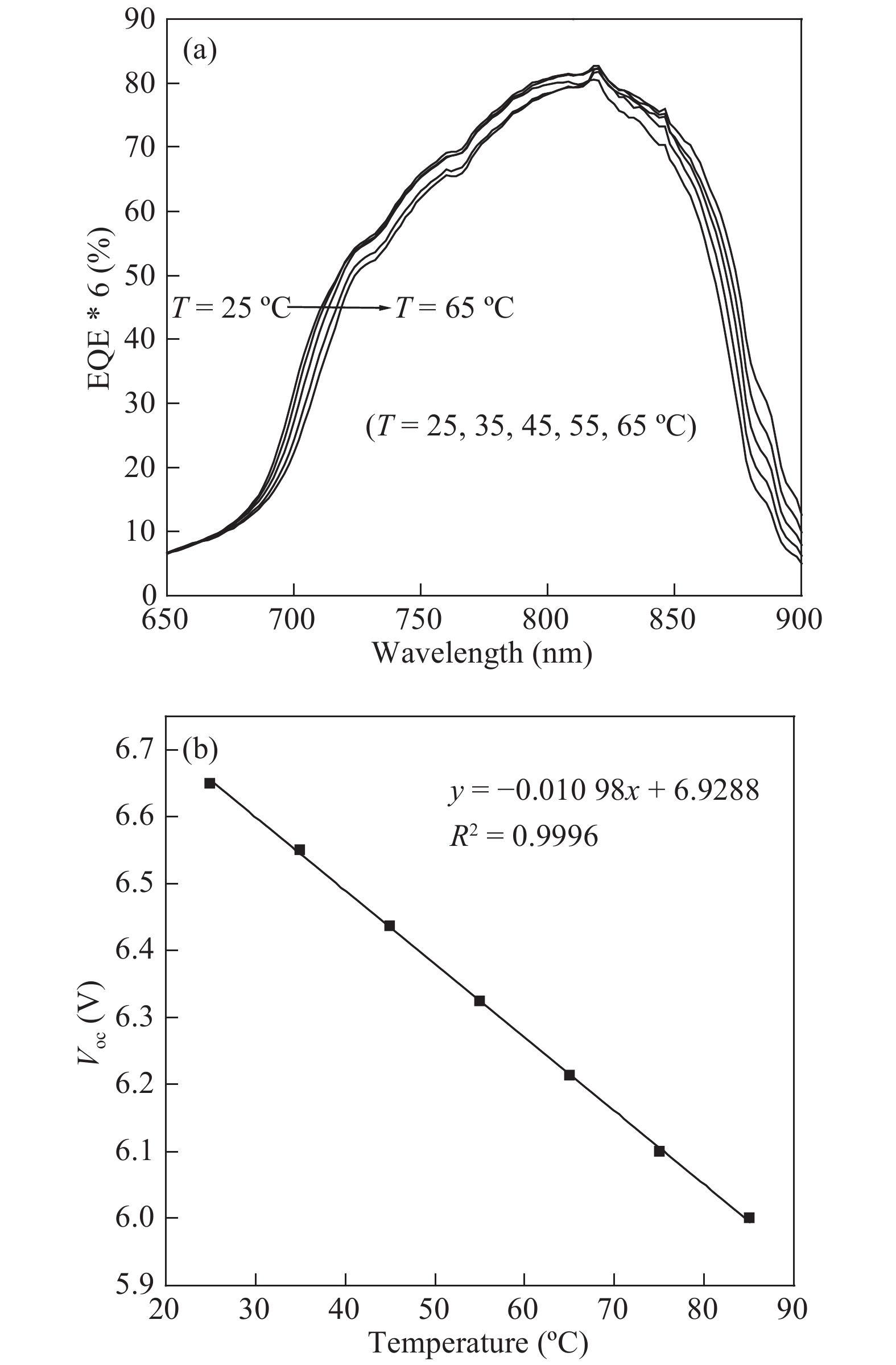
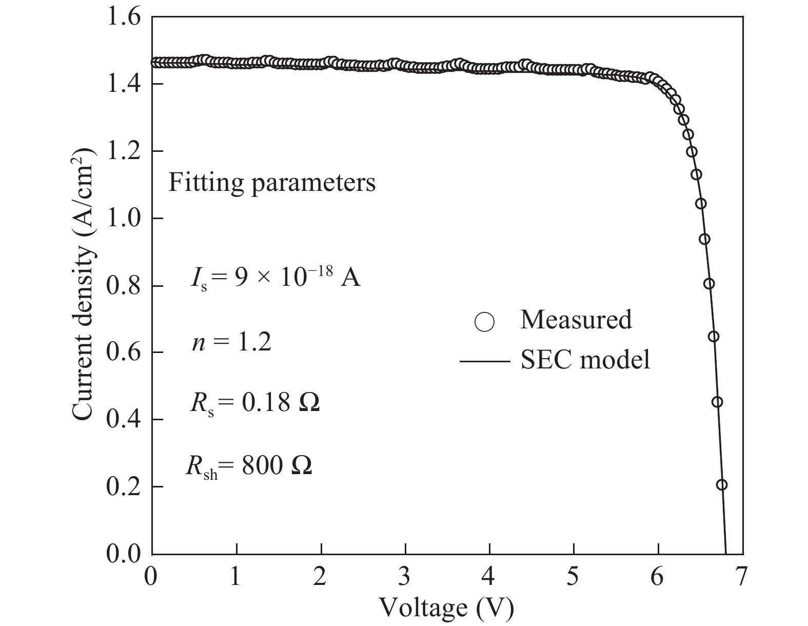
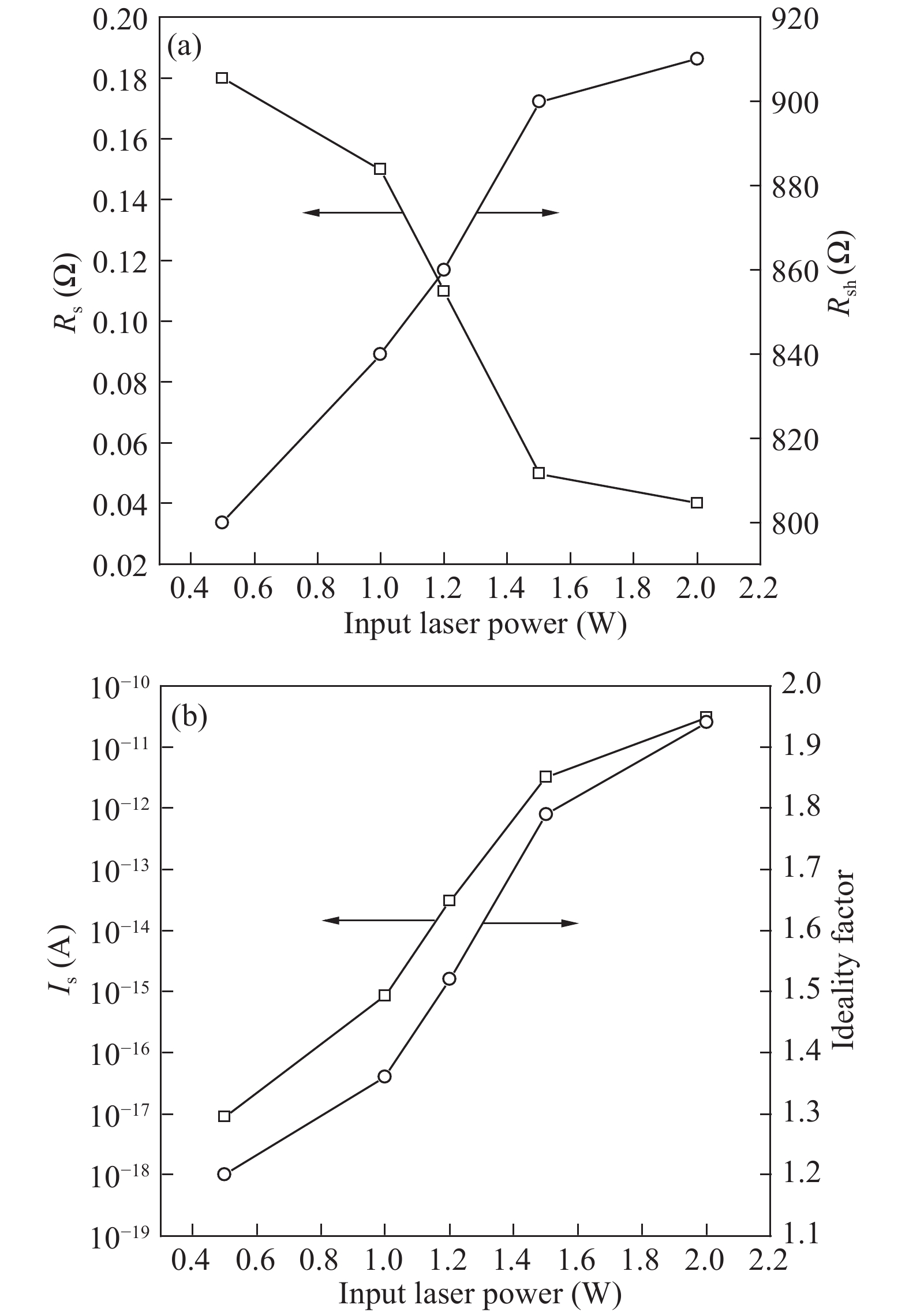
Six-junction vertically-stacked GaAs laser power converters (LPCs) with n+-GaAs/p+-Al0.37Ga0.63As tunnel junctions have been designed and grown by metal-organic chemical vapor deposition for converting the power of 808 nm lasers. The LPC chips are characterized by measuring current–voltage (I–V) characteristics under 808 nm laser illumination, and a maximum conversion efficiency ηc of 53.1% is obtained for LPCs with an aperture diameter of 2 mm at an input laser power of 0.5 W. In addition, the characteristics of the LPCs are analyzed by a standard equivalent-circuit model, and the reverse saturation current, ideality factor, series resistance and shunt resistance are extracted by fitting of the I–V curves.
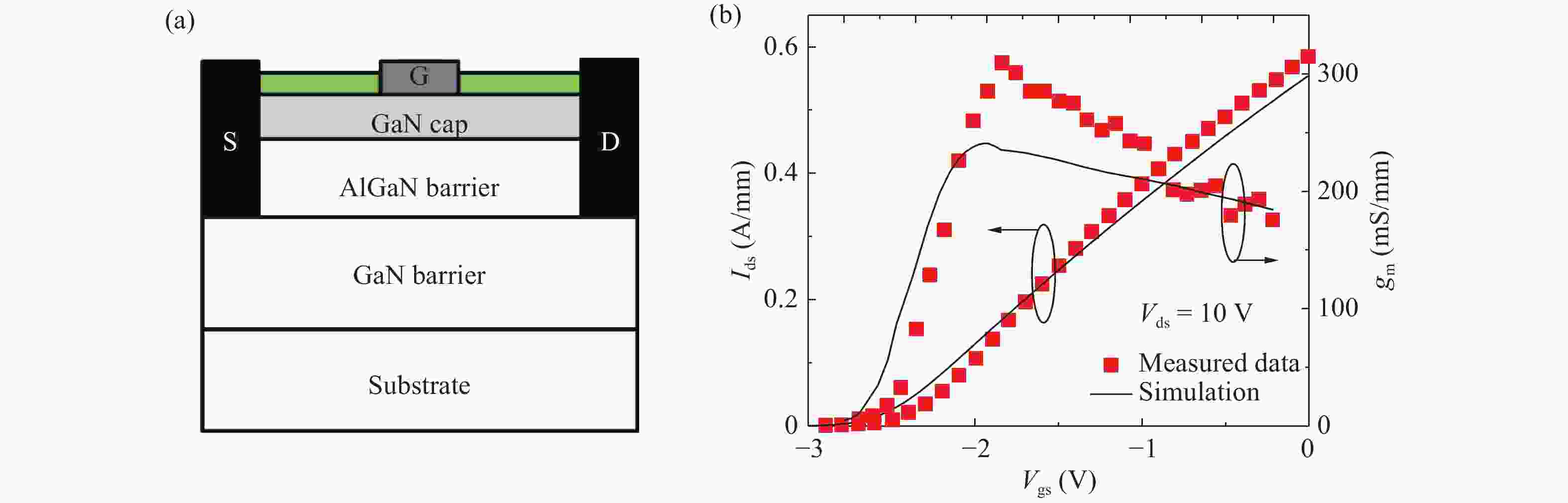
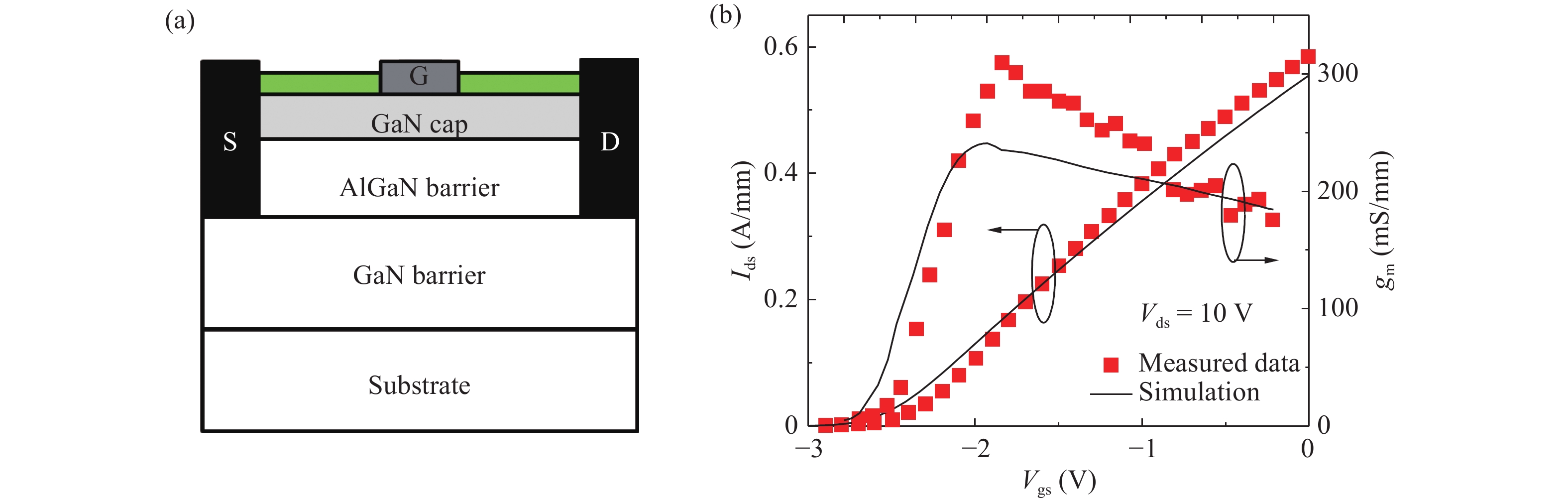
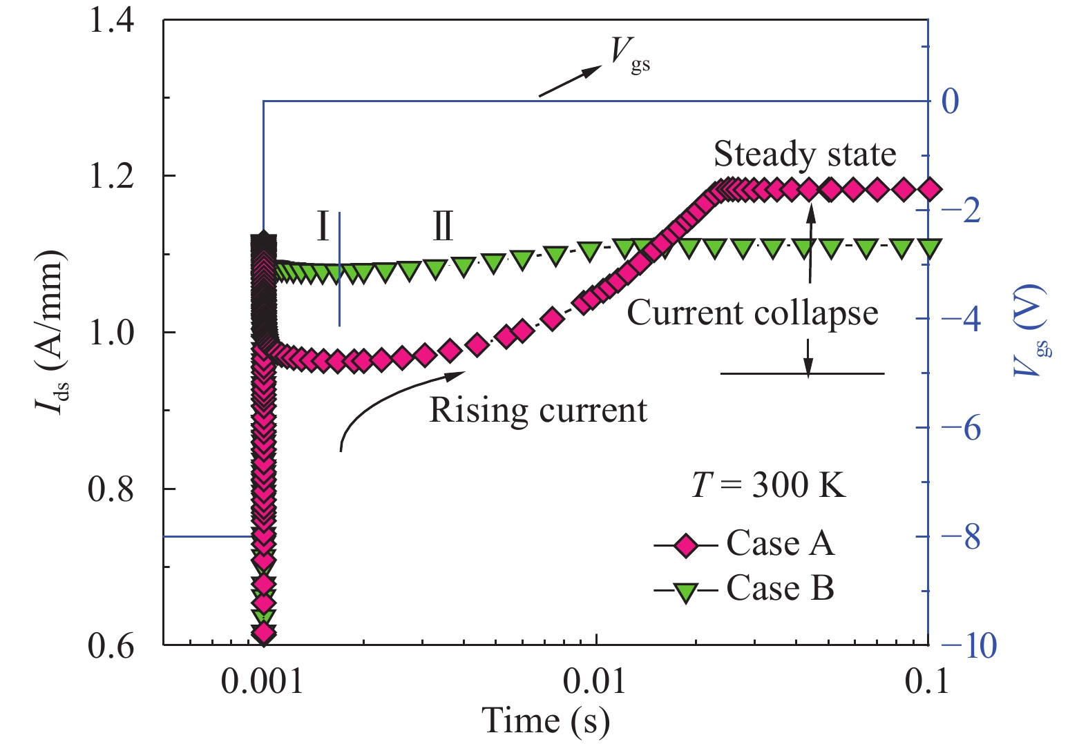
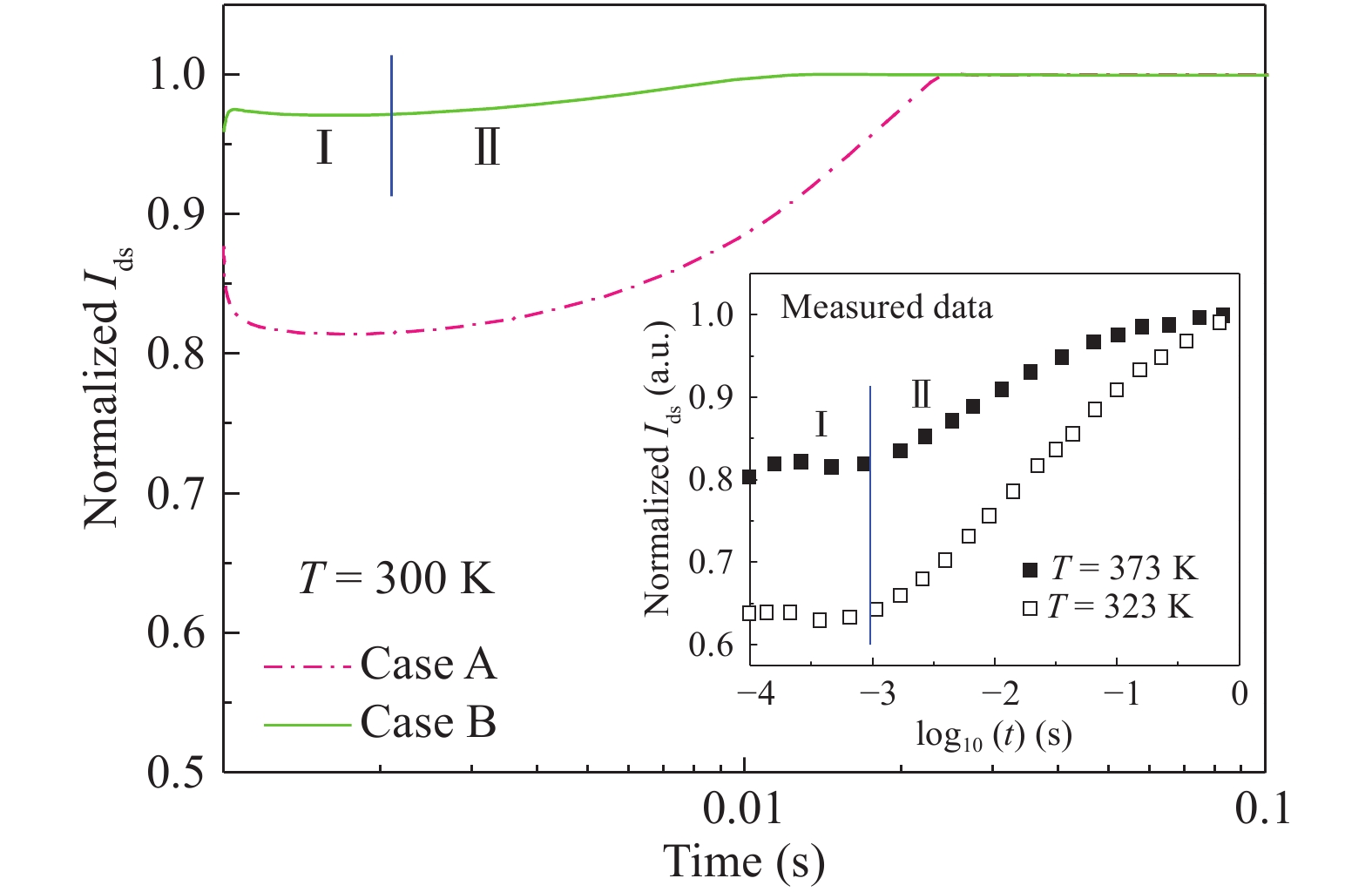
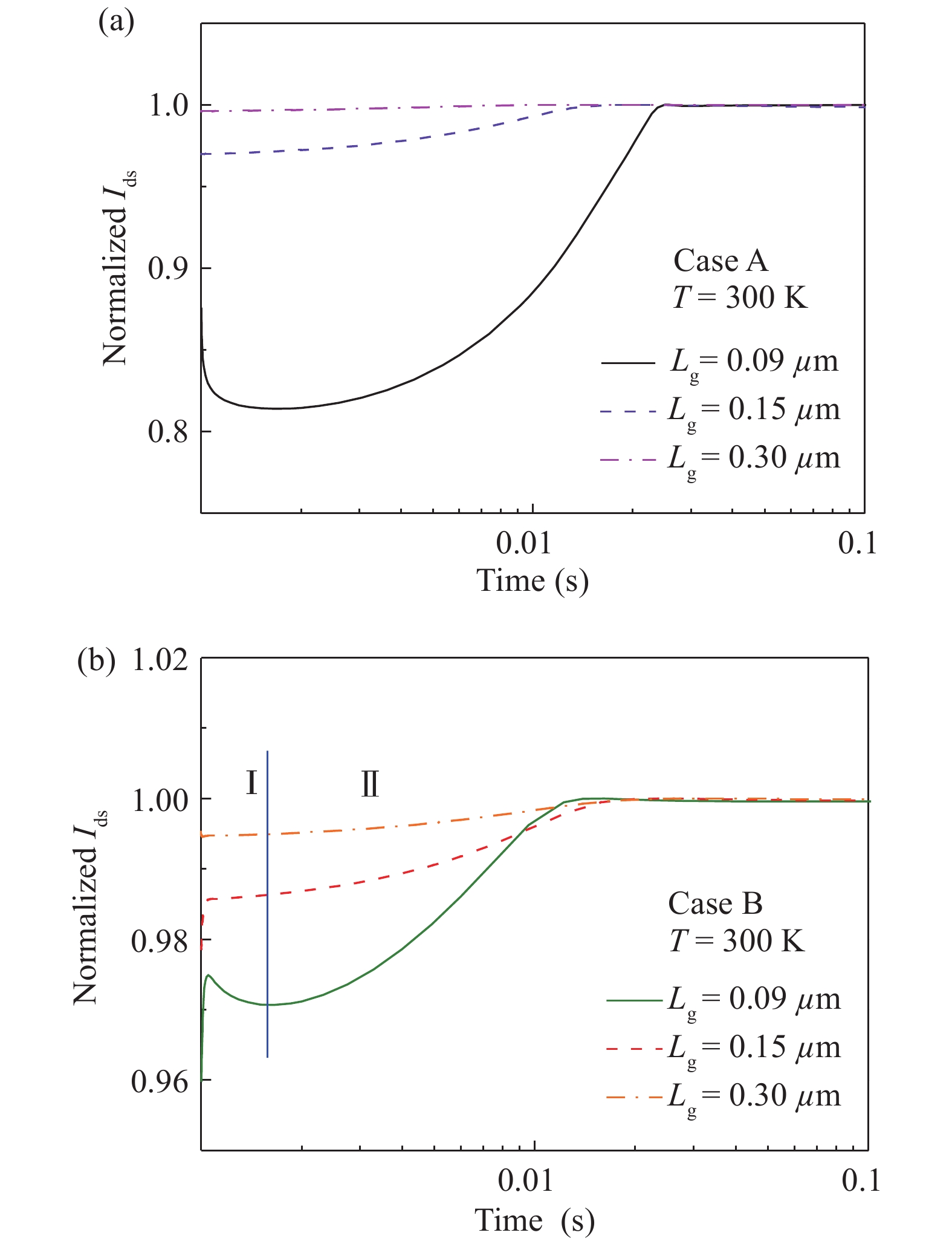
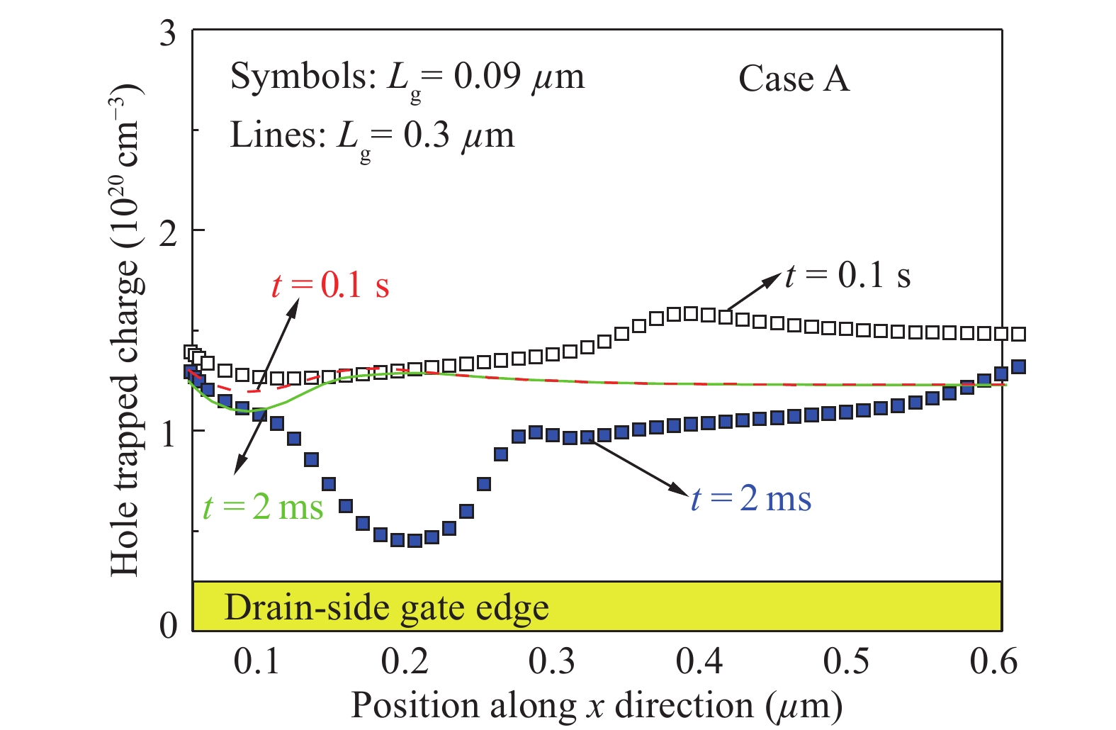
Trap-induced current collapse has become one of the critical issues hindering the improvement of GaN-based microwave power devices. It is difficult to study the behavior of each trapping effect separately with the experimental measurement. Transient simulation is a useful technique for analyzing the mechanism of current collapse. In this paper, the coeffect of surface- and bulk-trapping behaviors on the performance of AlGaN/GaN HEMTs is investigated based on the two-dimensional (2D) transient simulation. In addition, the mechanism of trapping effects is analyzed from the aspect of device physics. Two simulation models with different types of traps are used for comparison, and the simulated results reproduced the experimental measured data. It is found that the final steady-state current decreases when both the surface and bulk traps are taken into account in the model. However, contrary to the expectation, the total current collapse is dramatically reduced (e.g. from 18% to 4% for the 90 nm gate-length device). The results suggest that the surface-related current collapse of GaN-based HEMTs may be mitigated in some degree due to the participation of bulk traps with short time constant. The work in this paper will be helpful for further optimization design of material and device structures.


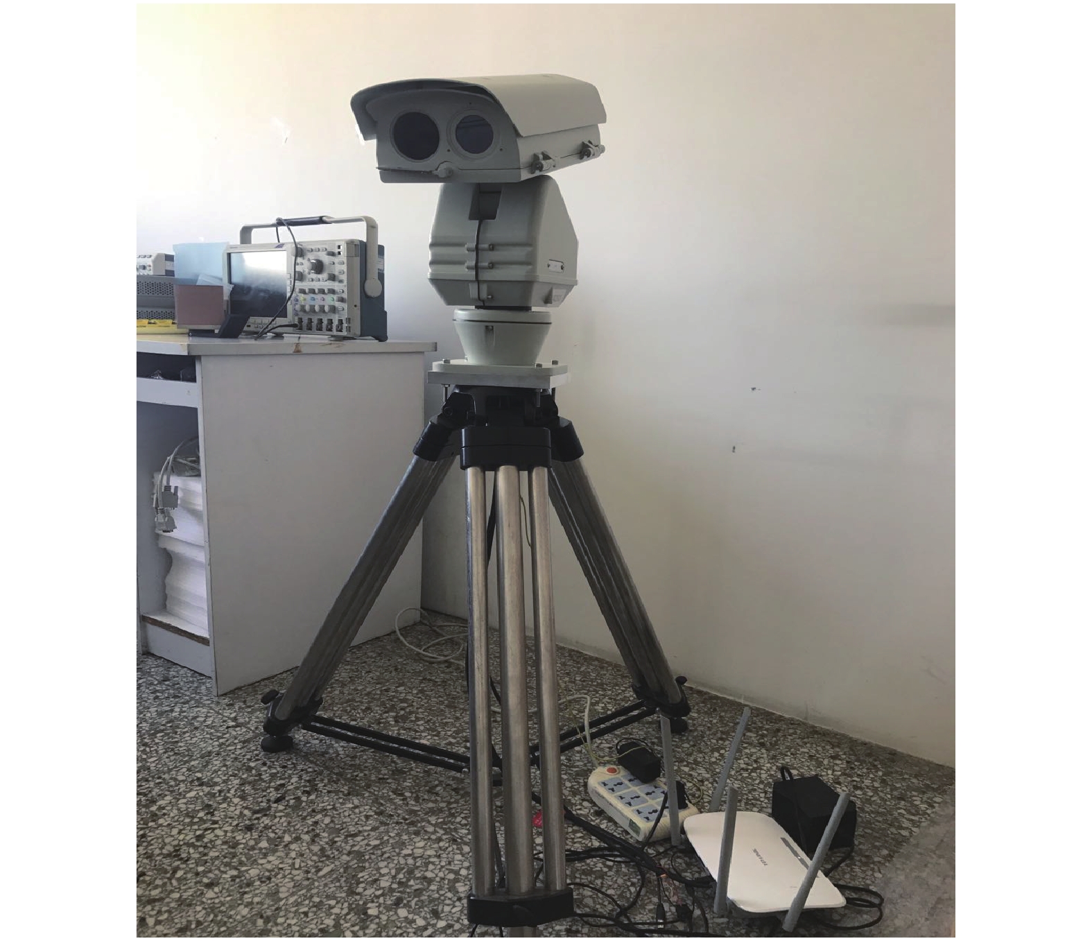
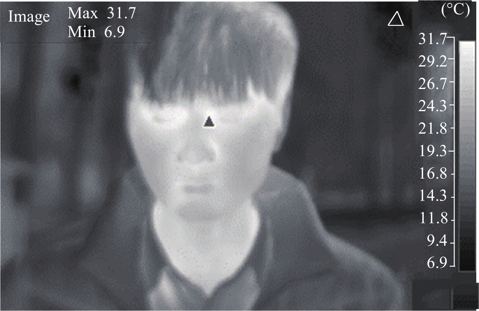
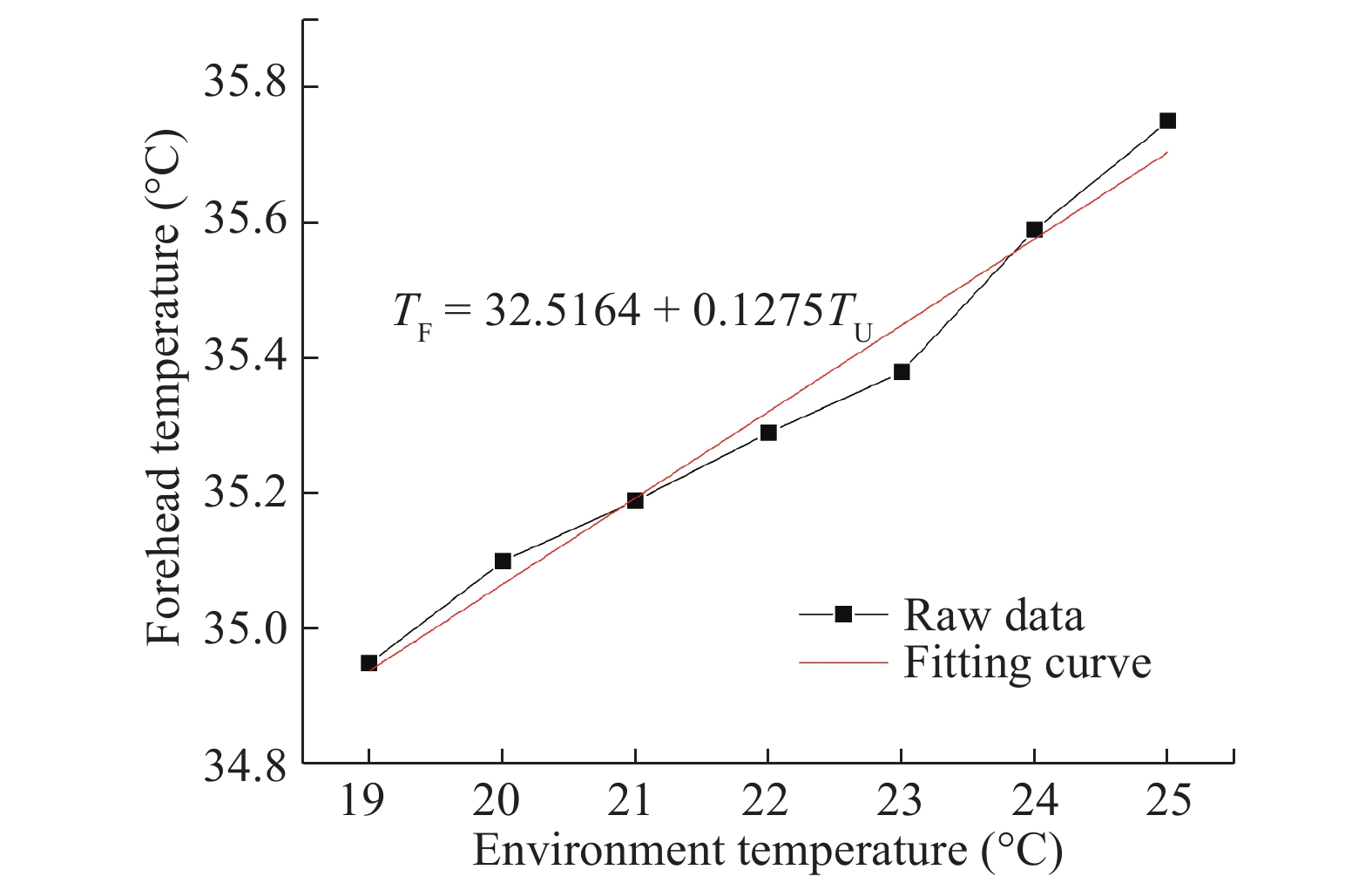
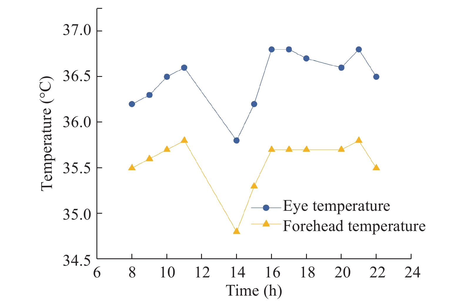
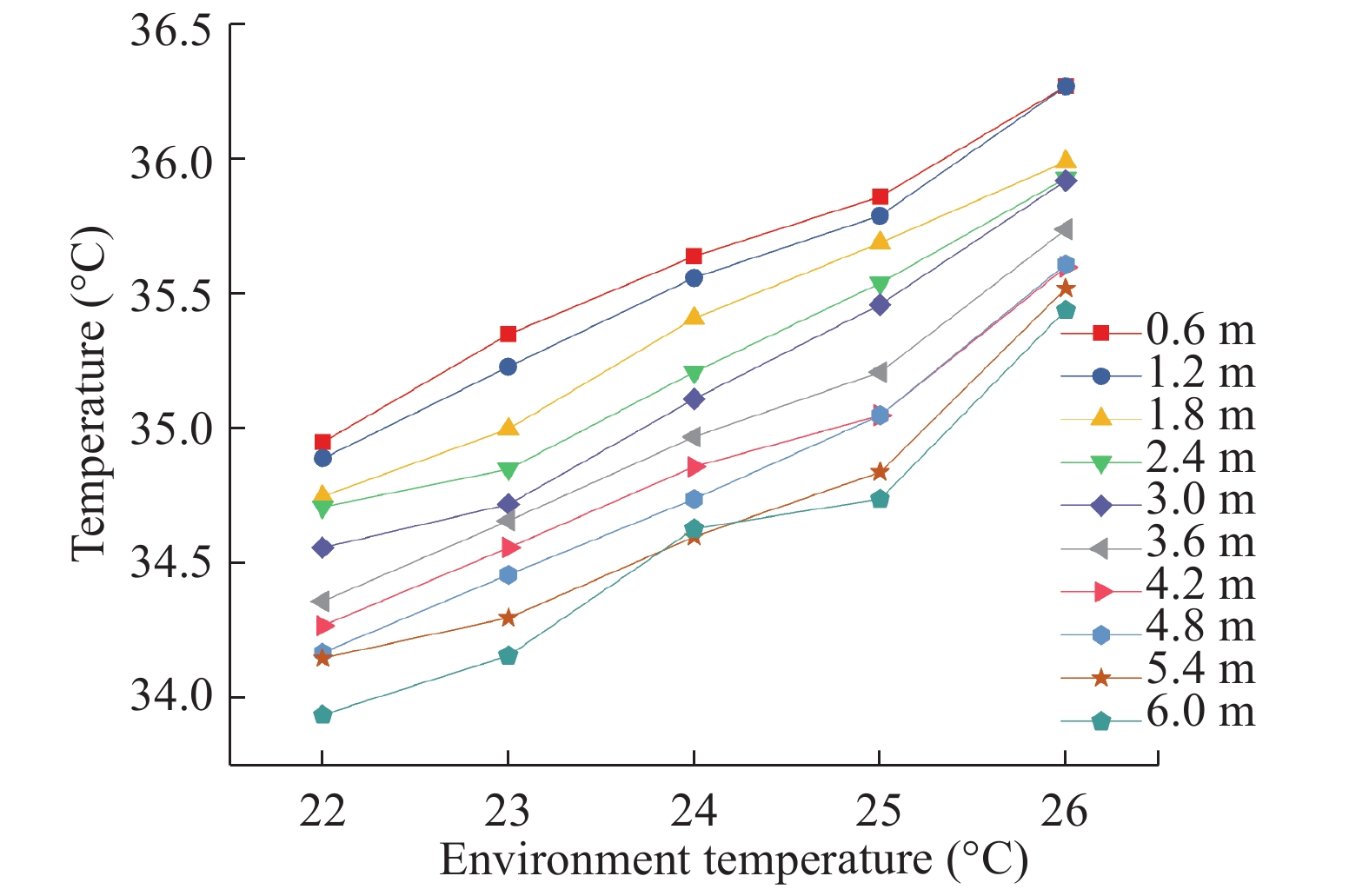
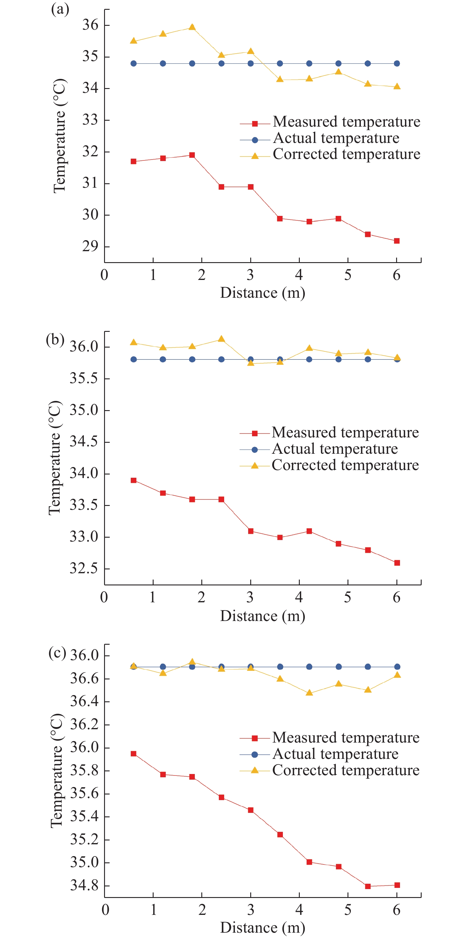
In order to reduce the temperature measurement error with the uncooled infrared thermal imager, experiments were conducted to evaluate the effects of environment temperature and measurement distance on the measurement error of human eye temperature. First, the forehead temperature was used as an intermediate variable to obtain the actual temperature of human eyes. Then, the effects of environment temperature and measurement distance on the temperature measurement were separately analyzed. Finally, an empirical model was established to correlate actual eye temperature with the measured temperature, environment temperature, and measurement distance. To verify the formula, three different environment temperatures were tested at different distances. The measurement errors were substantially reduced using the empirical model for temperature correction. The results show that this method can effectively improve the accuracy of temperature measurement using the infrared thermal imager.

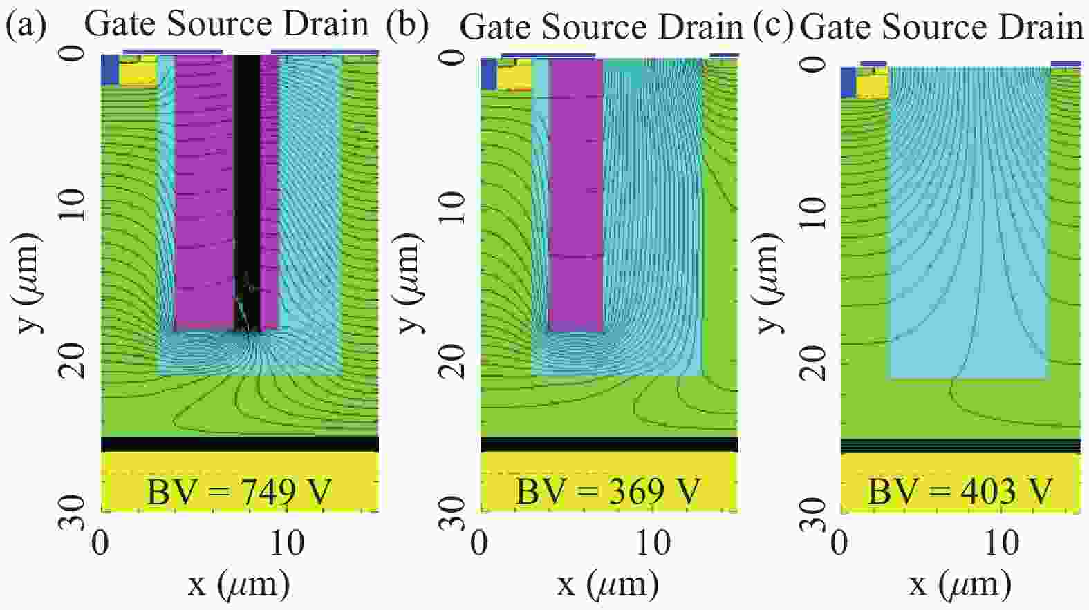
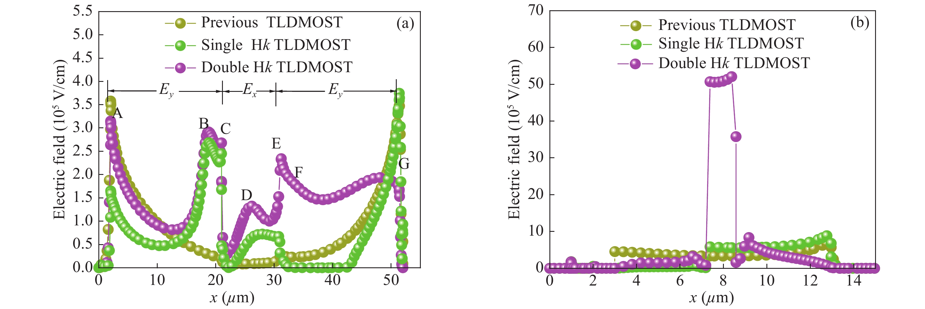
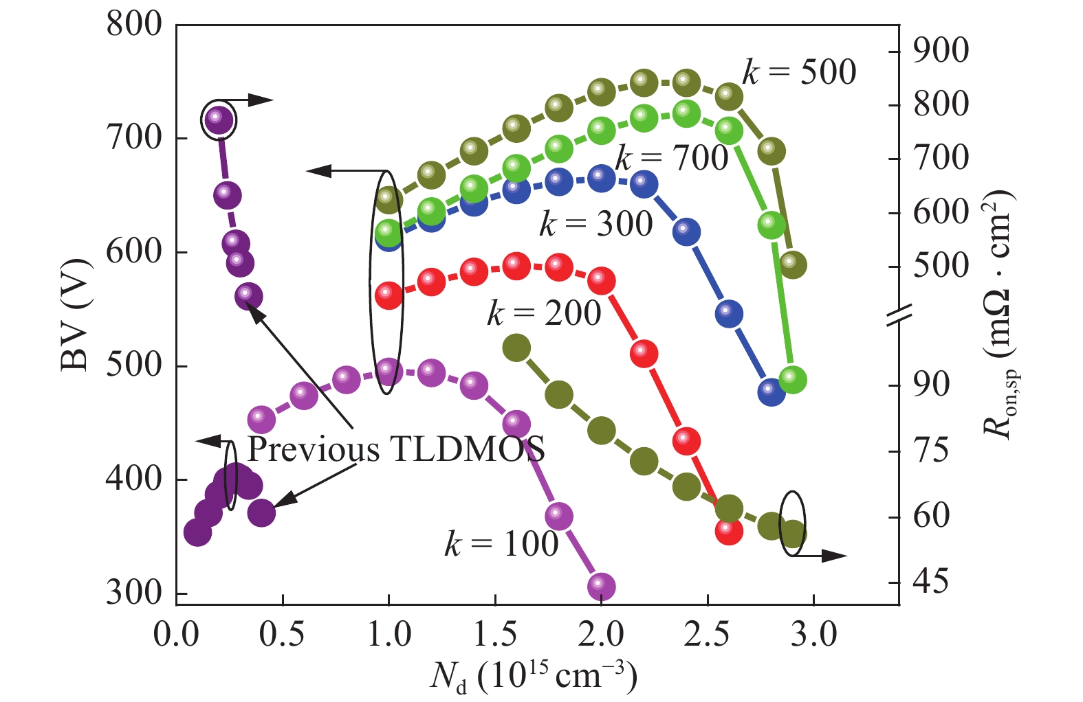
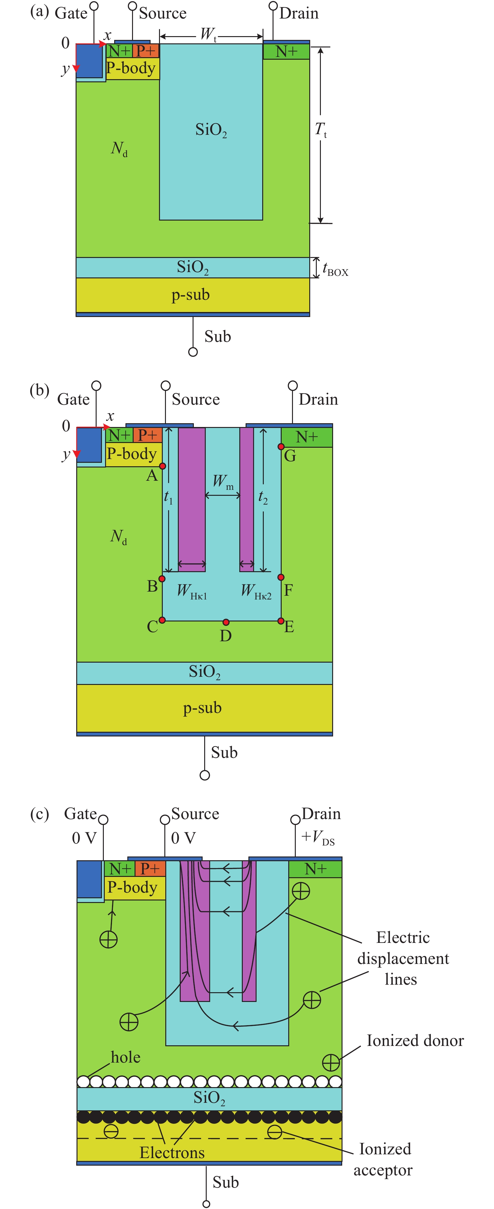
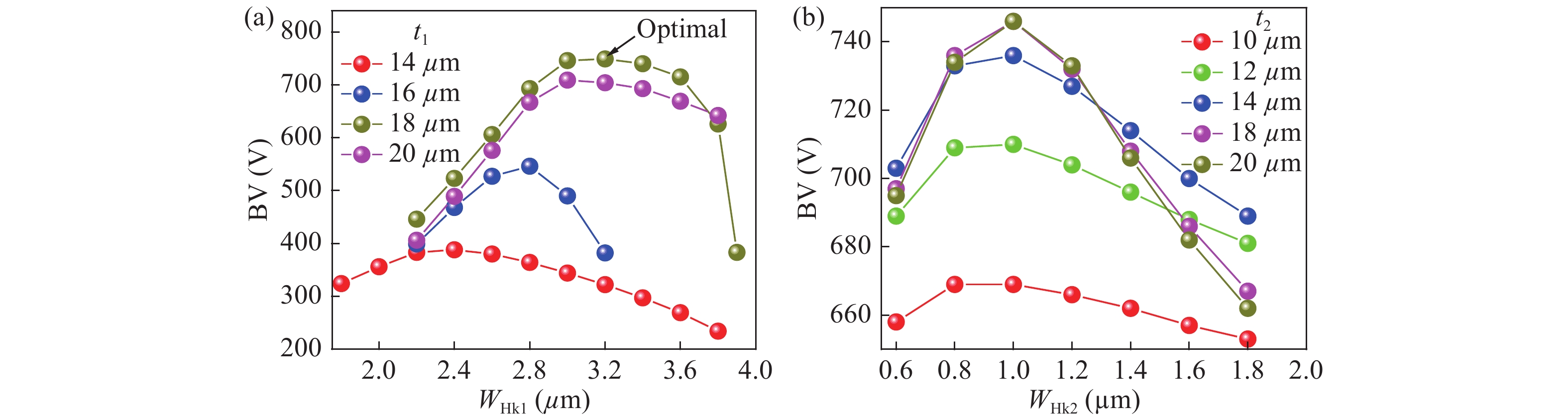
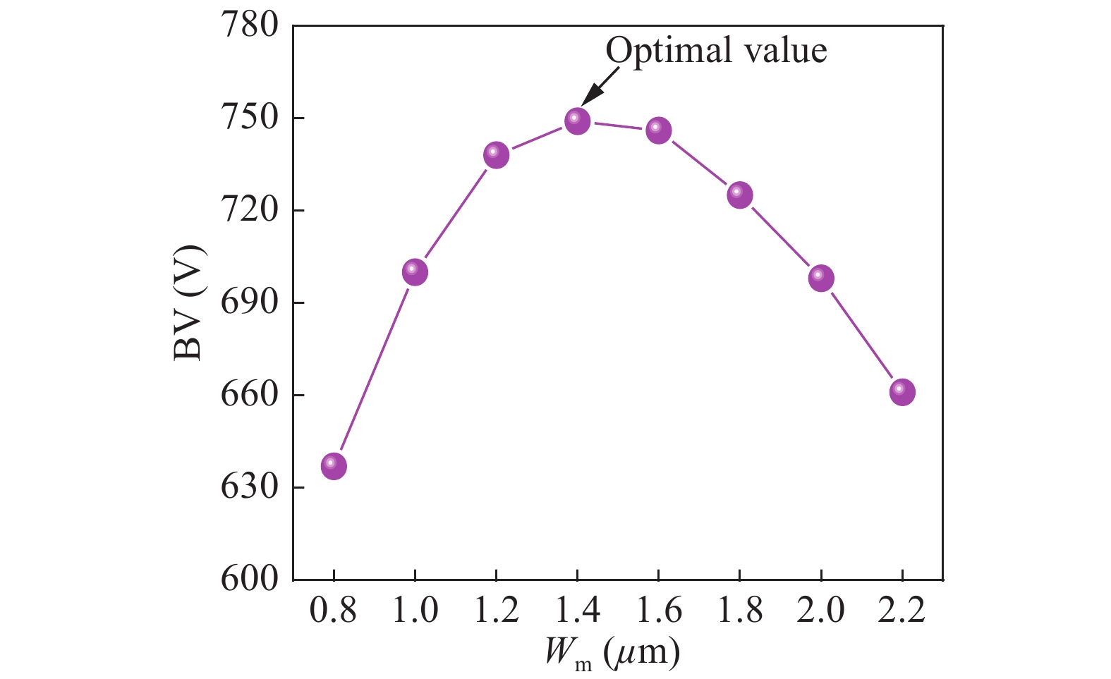
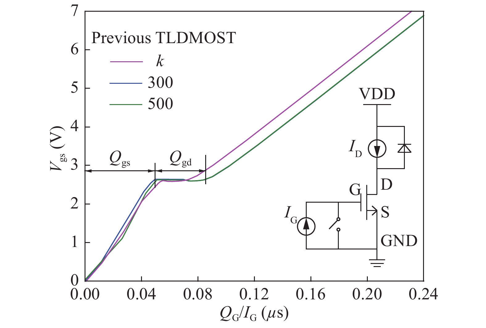
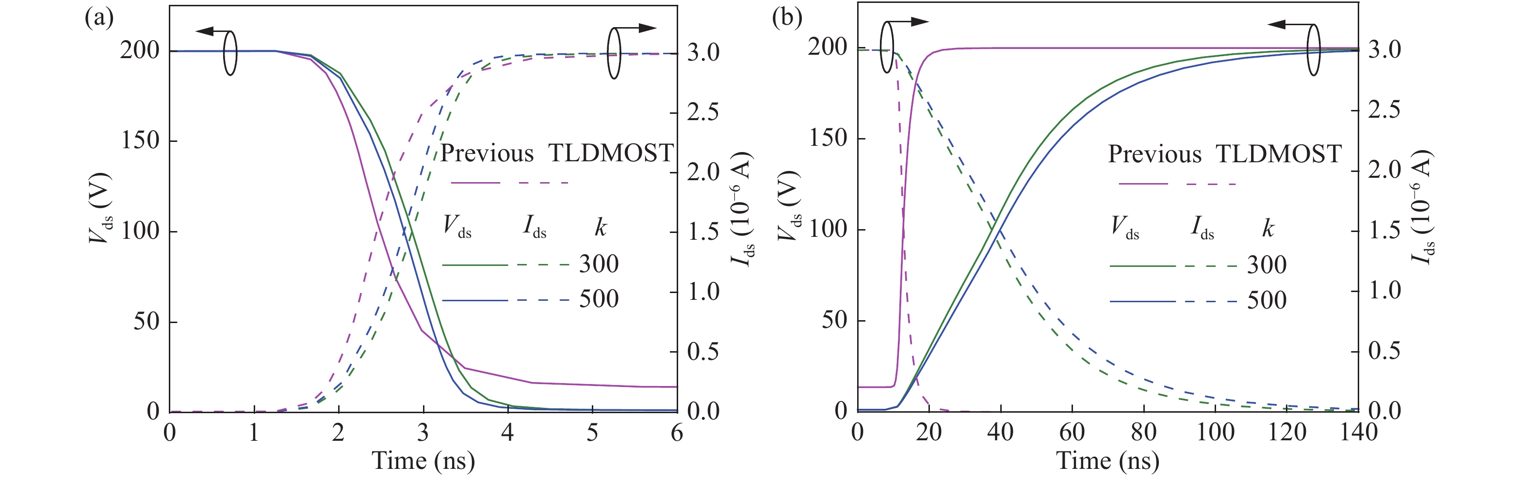
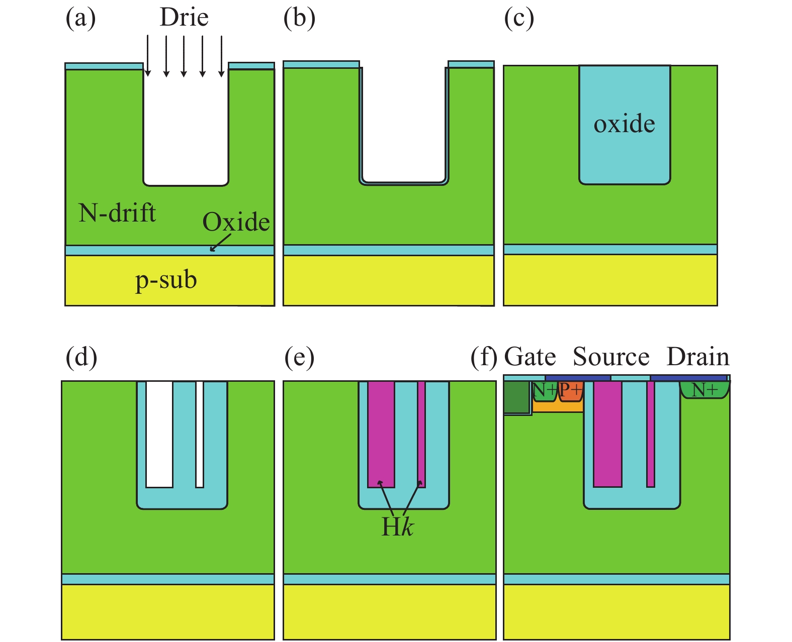
An SOI trench LDMOST (TLDMOST) with ultra-low specific on-resistance (Ron,sp) is proposed. It features double vertical high-k insulator pillars (Hk1 and Hk2) in the oxide trench, which are connected to the source electrode and drain electrode, respectively. Firstly, under reverse bias voltage, most electric displacement lines produced by the charges of the depleted drift region in the source side go through the Hk1, and thus the average electric field strength under the source can be enhanced. Secondly, two additional electric field peaks are induced by the Hk1, which further modulate the electric field in the drift region under the source. Thirdly, most electric displacement lines produced by the charges of the depleted drift region in the drain side enter into the Hk2. This not only introduces one more electric field peak at the corner of the oxide trench around the Hk2, but also forms the enhanced vertical reduced surface field effect, which modulates the electric field in the drift region under the drain. With the effects of the two Hk insulator pillars, the breakdown voltage (BV) and the drift region doping concentration are significantly improved. The simulation results indicate that compared with the oxide trench LDMOST (previous TLDMOST) with the same geometry, the proposed double Hk TLDMOST enhances the BV by 86% and reduces the Ron,sp by 88%.


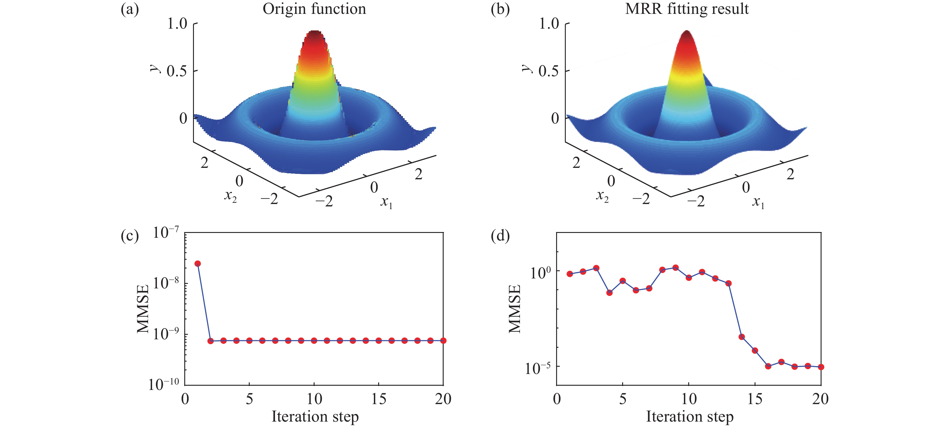
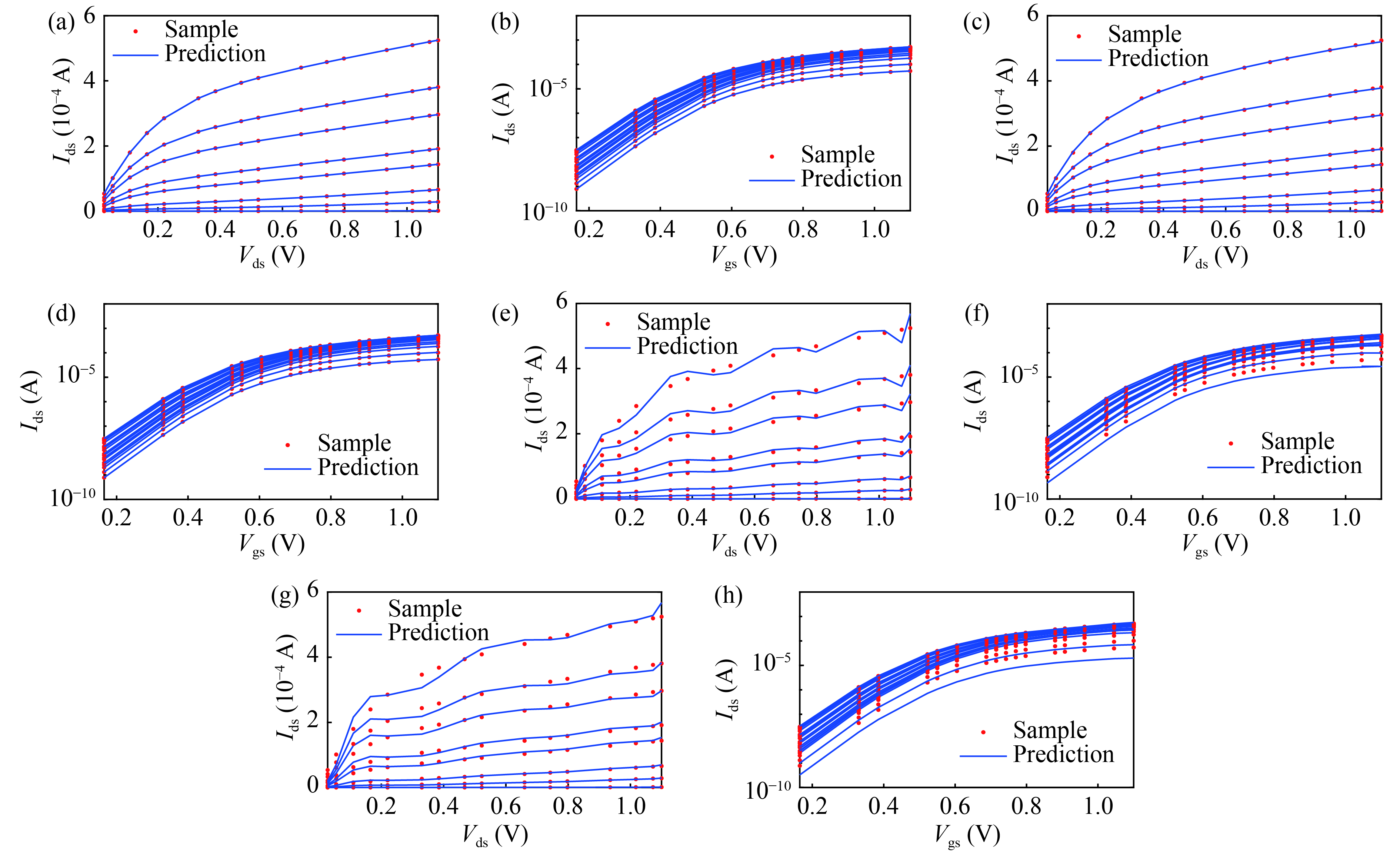
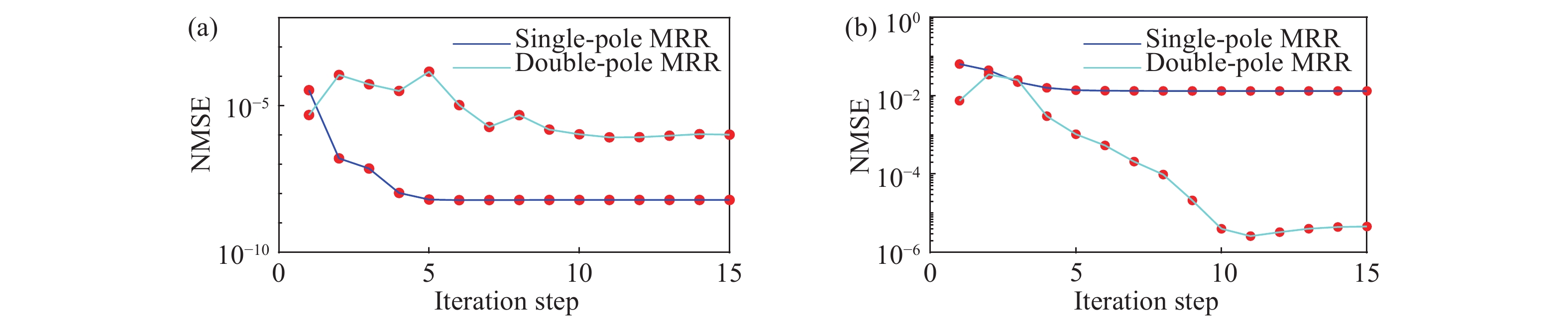
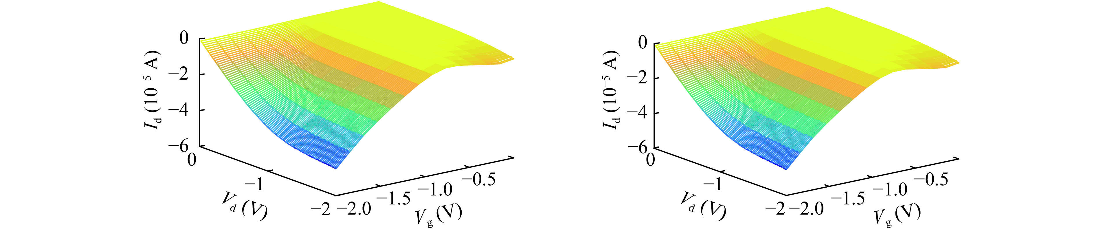
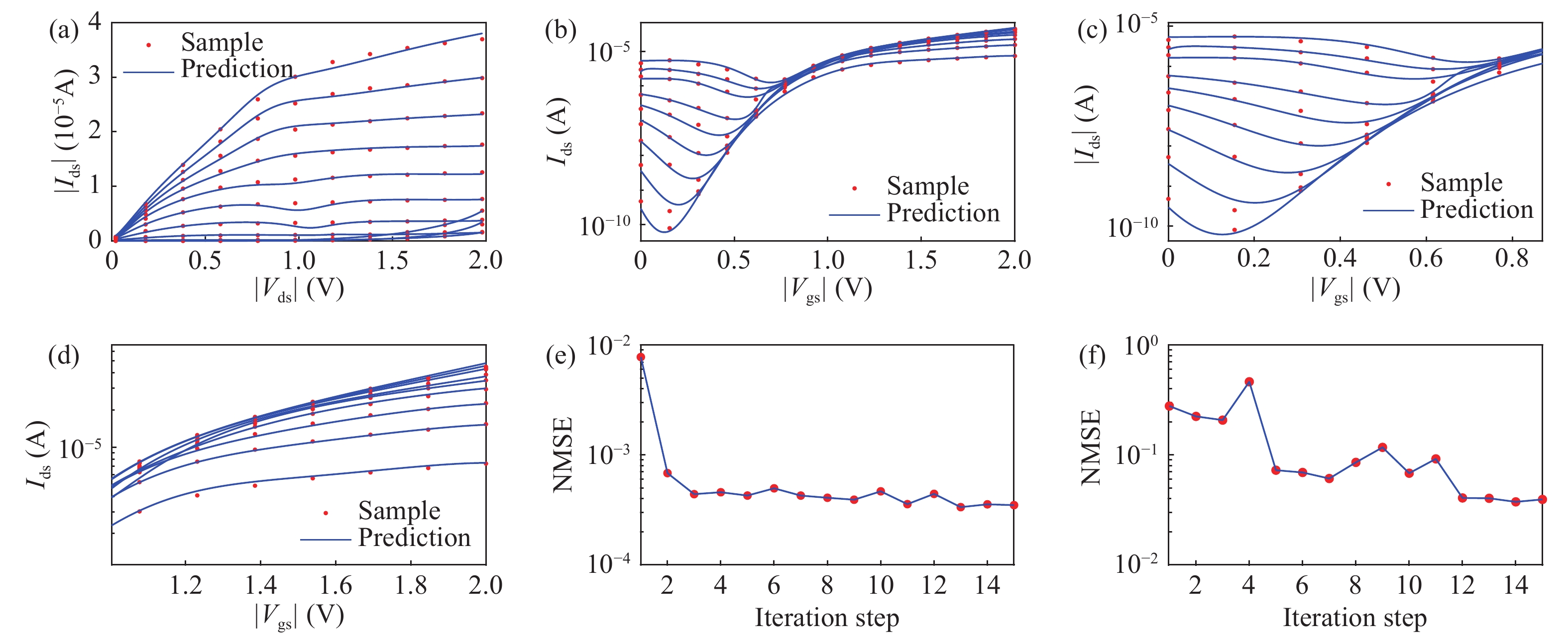
Physics equation-based semiconductor device modeling is accurate but time and money consuming. The need for studying new material and devices is increasing so that there has to be an efficient and accurate device modeling method. In this paper, two methods based on multivariate rational regression (MRR) for device modeling are proposed. They are single-pole MRR and double-pole MRR. The two MRR methods are proved to be powerful in nonlinear curve fitting and have good numerical stability. Two methods are compared with OLS and LASSO by fitting the SMIC 40 nm MOS-FET I–V characteristic curve and the normalized mean square error of Single-pole MRR is


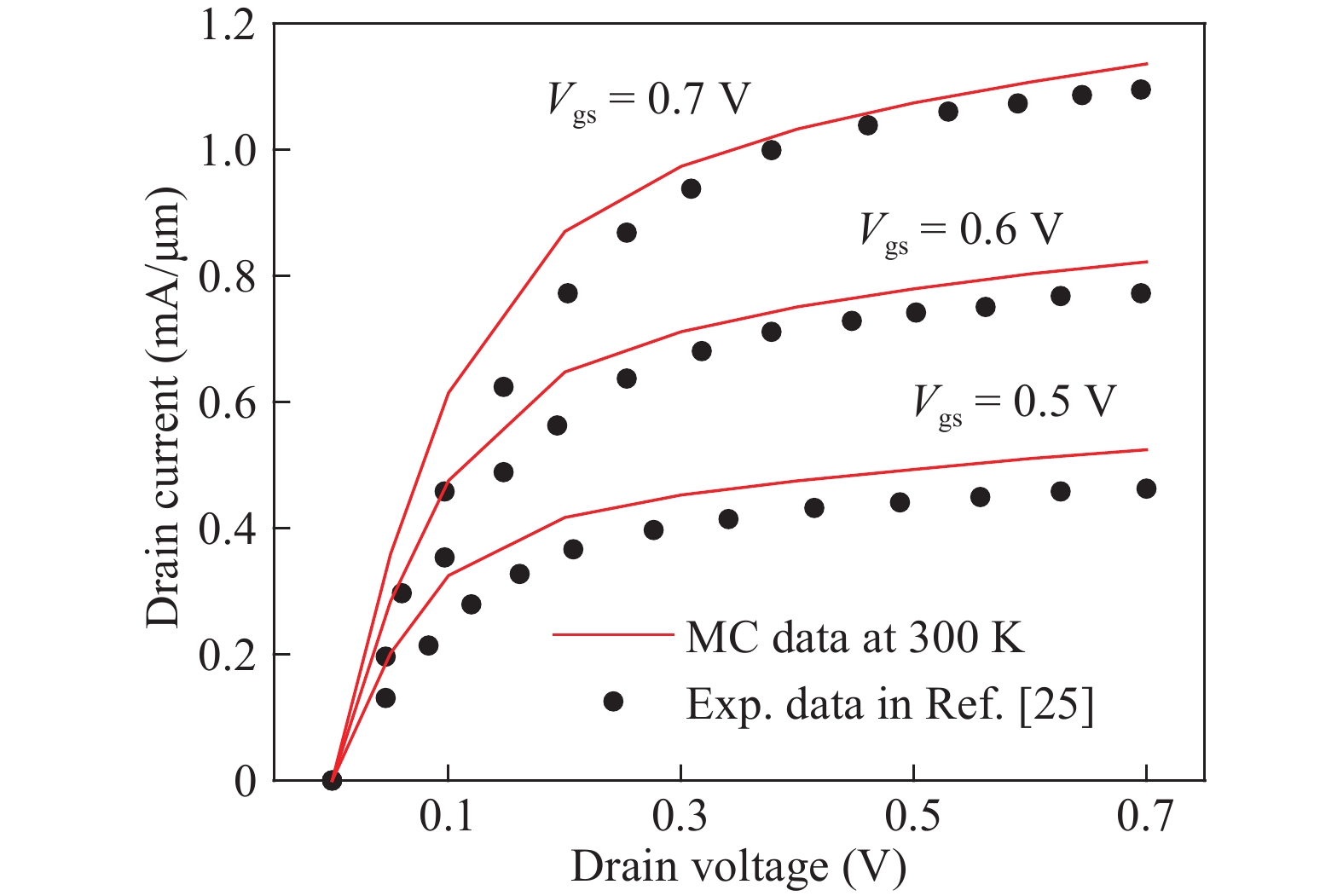
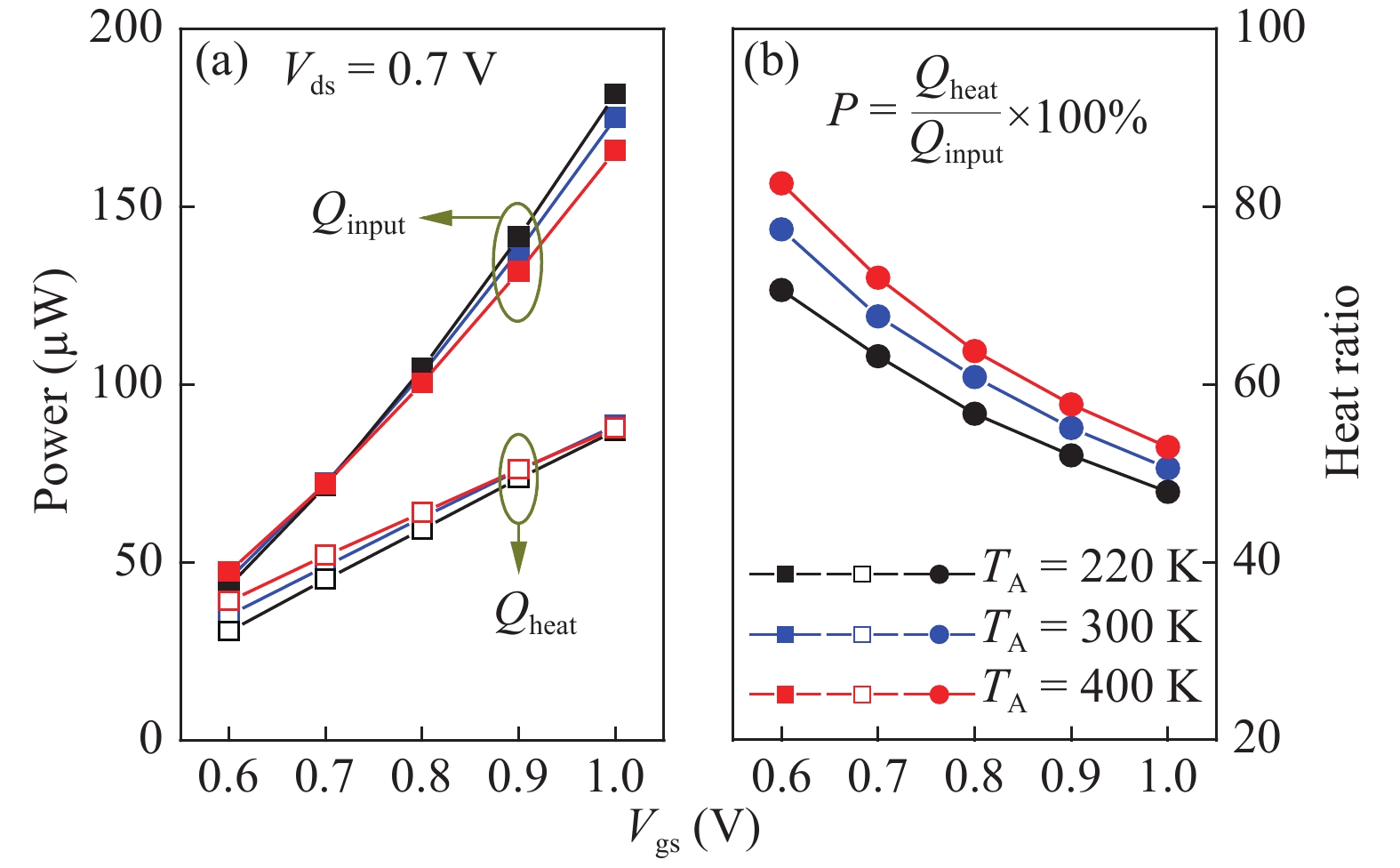
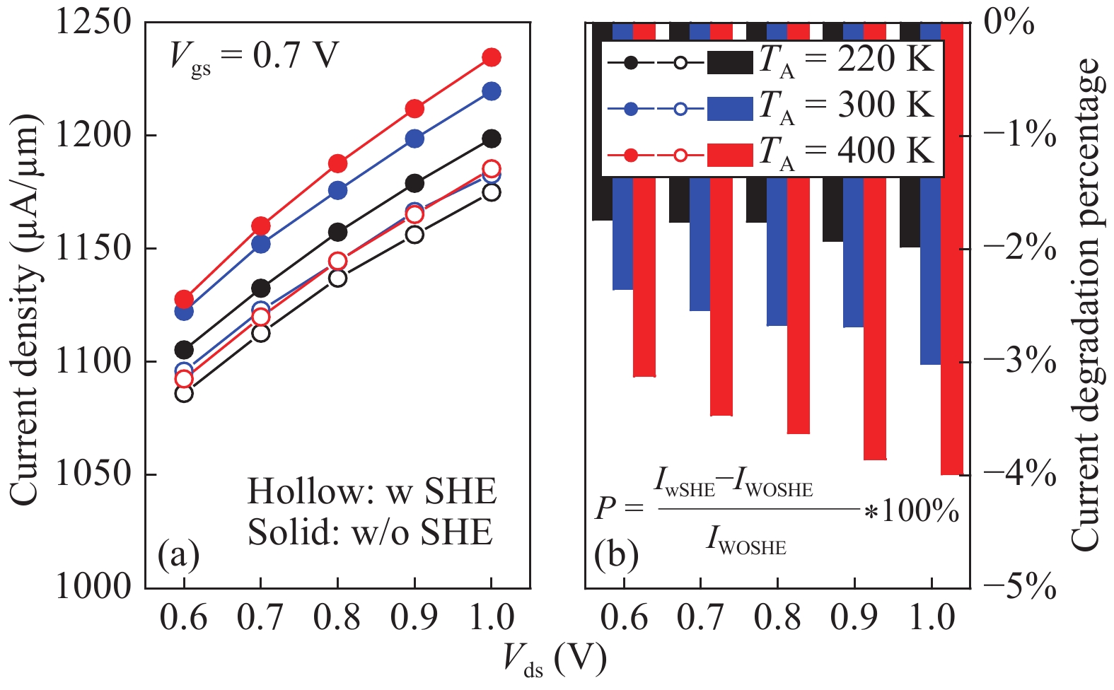
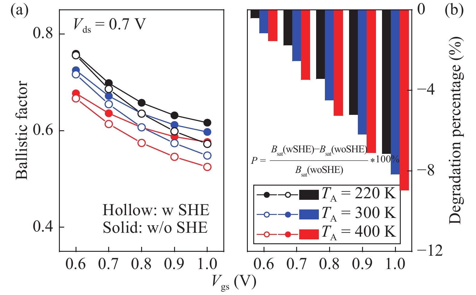
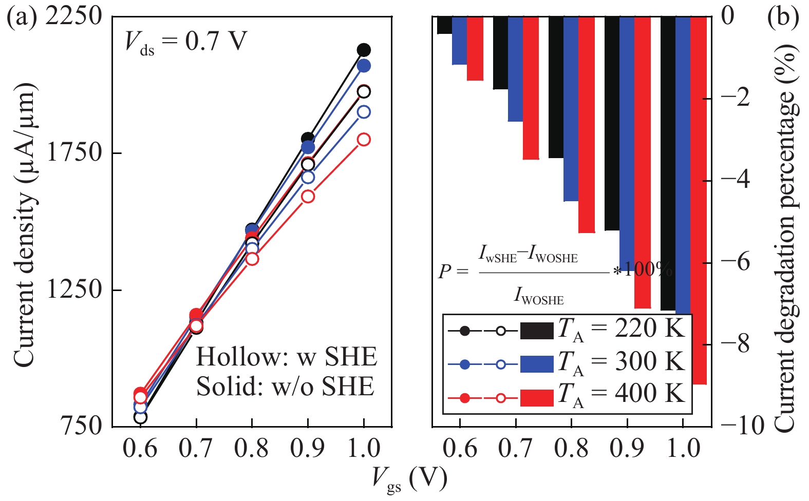
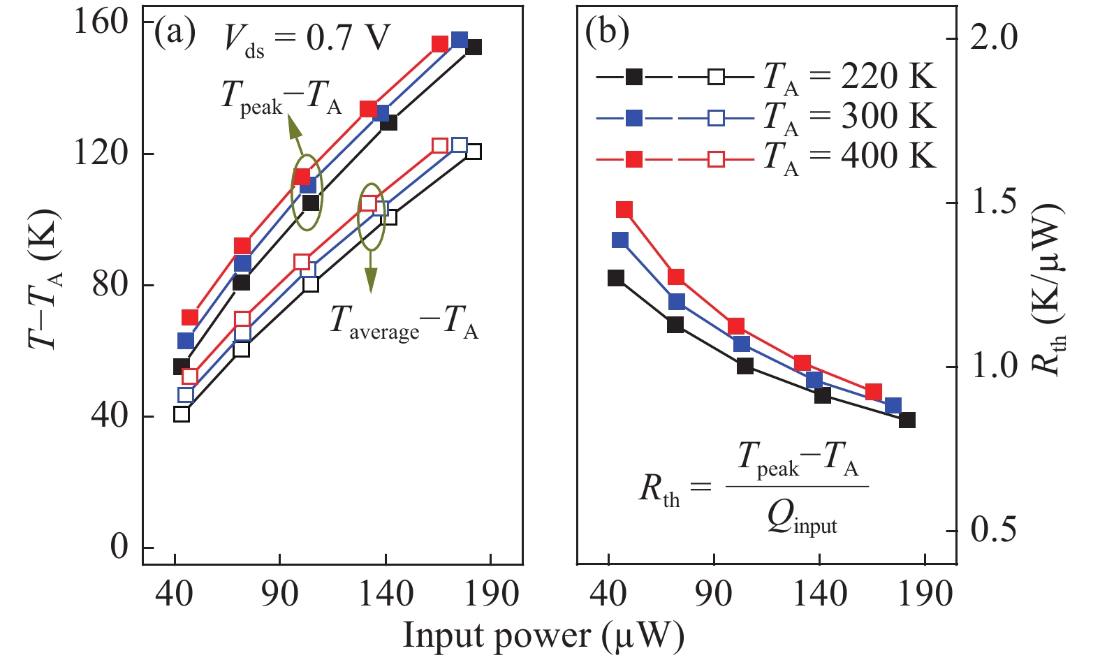
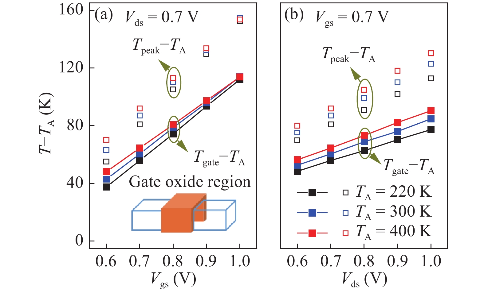
We use an electro-thermal coupled Monte Carlo simulation framework to investigate the self-heating effect (SHE) in 14 nm bulk nFinFETs with ambient temperature (TA) from 220 to 400 K. Based on this method, non-local heat generation can be achieved. Contact thermal resistances of Si/Metal and Si/SiO2 are selected to ensure that the source and drain heat dissipation paths are the first two heat dissipation paths. The results are listed below: (i) not all input power (Qinput) turns into heat generation in the device region and some is taken out by the thermal non-equilibrium carriers, owing to the serious non-equilibrium transport; (ii) a higher TA leads to a larger ratio of input power turning into heat generation in the device region at the same operating voltages; (iii) SHE can lead to serious degradation in the carrier transport, which will increase when TA increases; (iv) the current degradation can be 8.9% when Vds = 0.7 V, Vgs = 1 V and TA = 400 K; (v) device thermal resistance (Rth) increases with increasing of TA, which is seriously impacted by the non-equilibrium transport. Hence, the impact of TA should be carefully considered when investigating SHE in nanoscale devices.


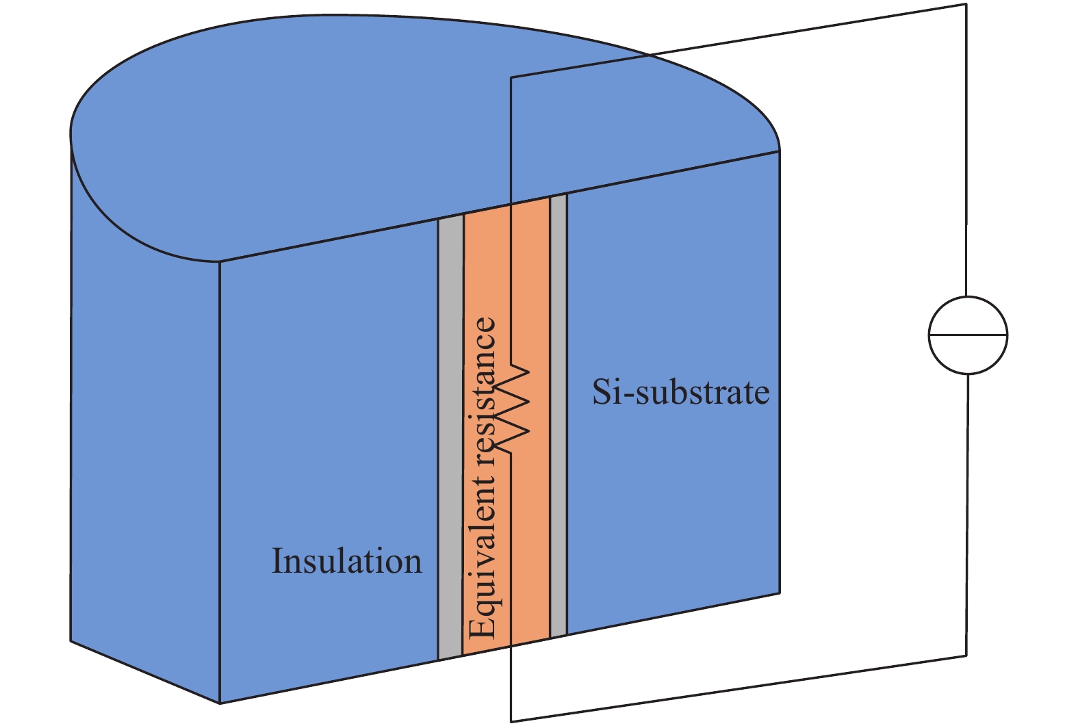
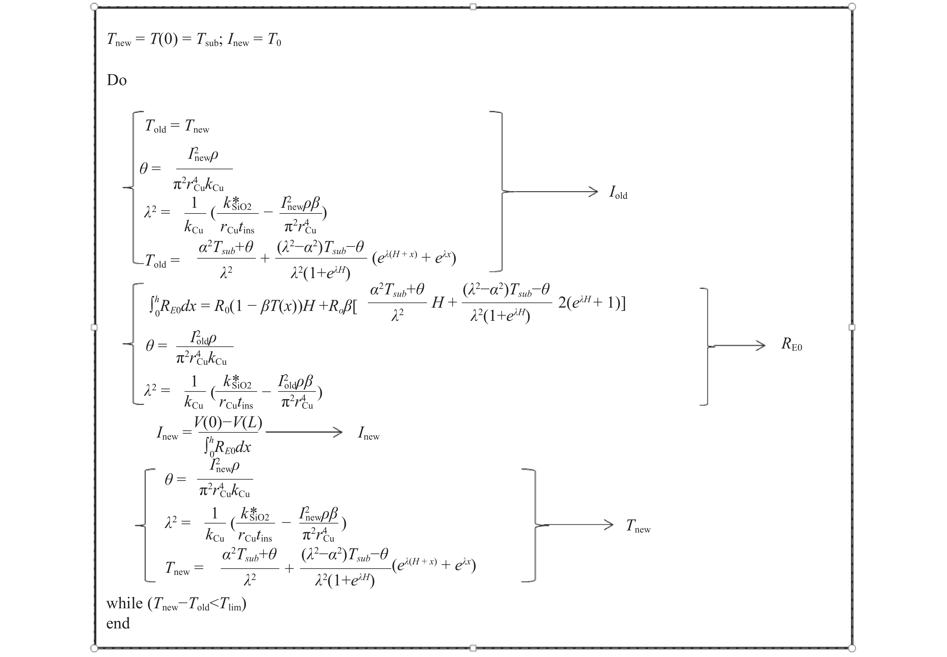
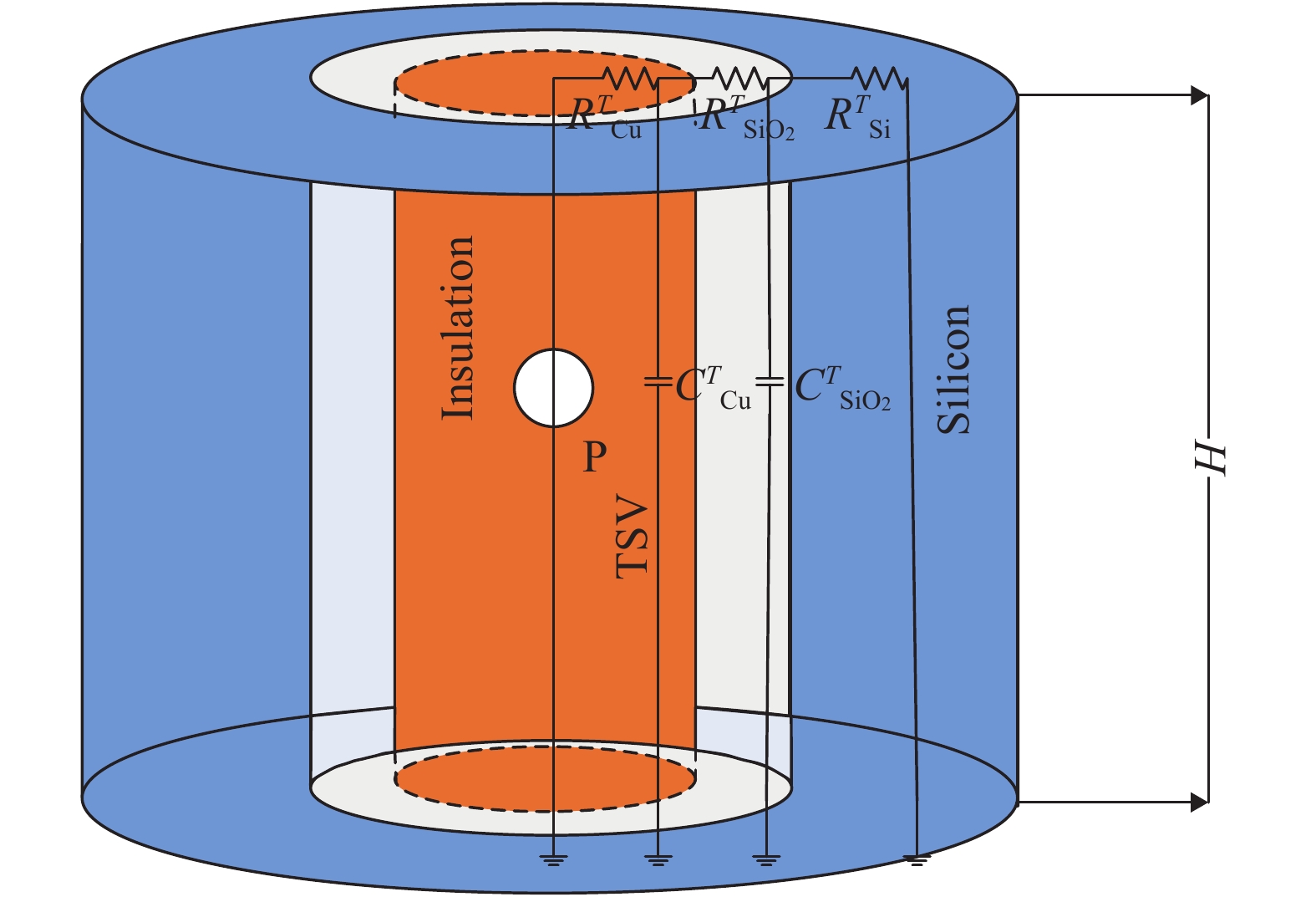
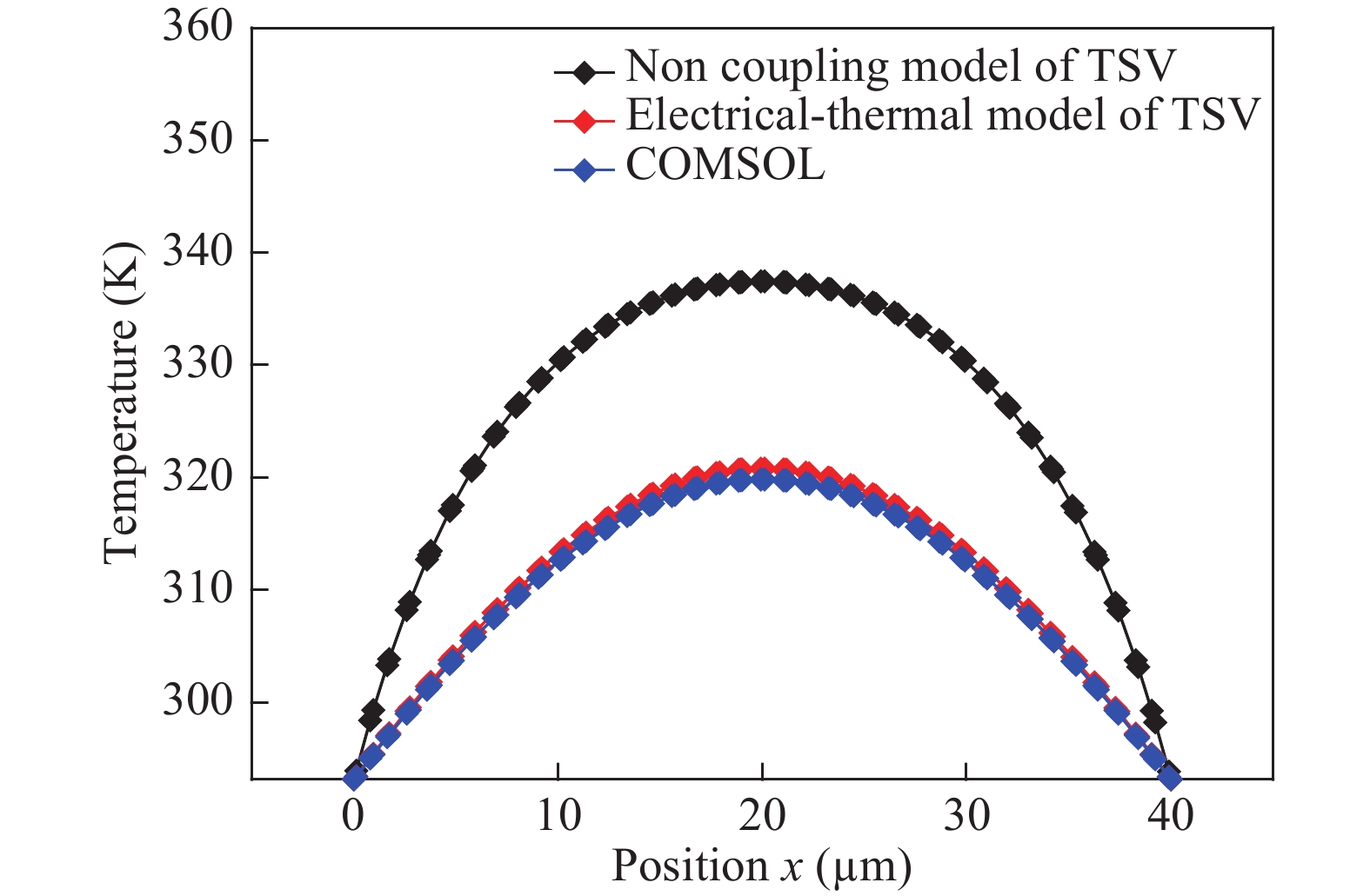
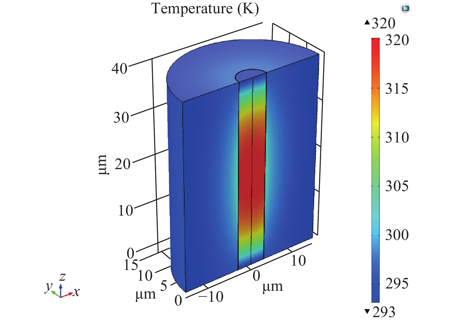
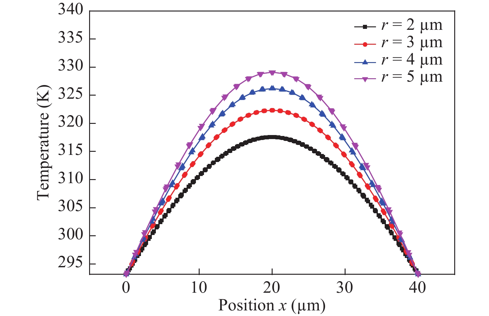
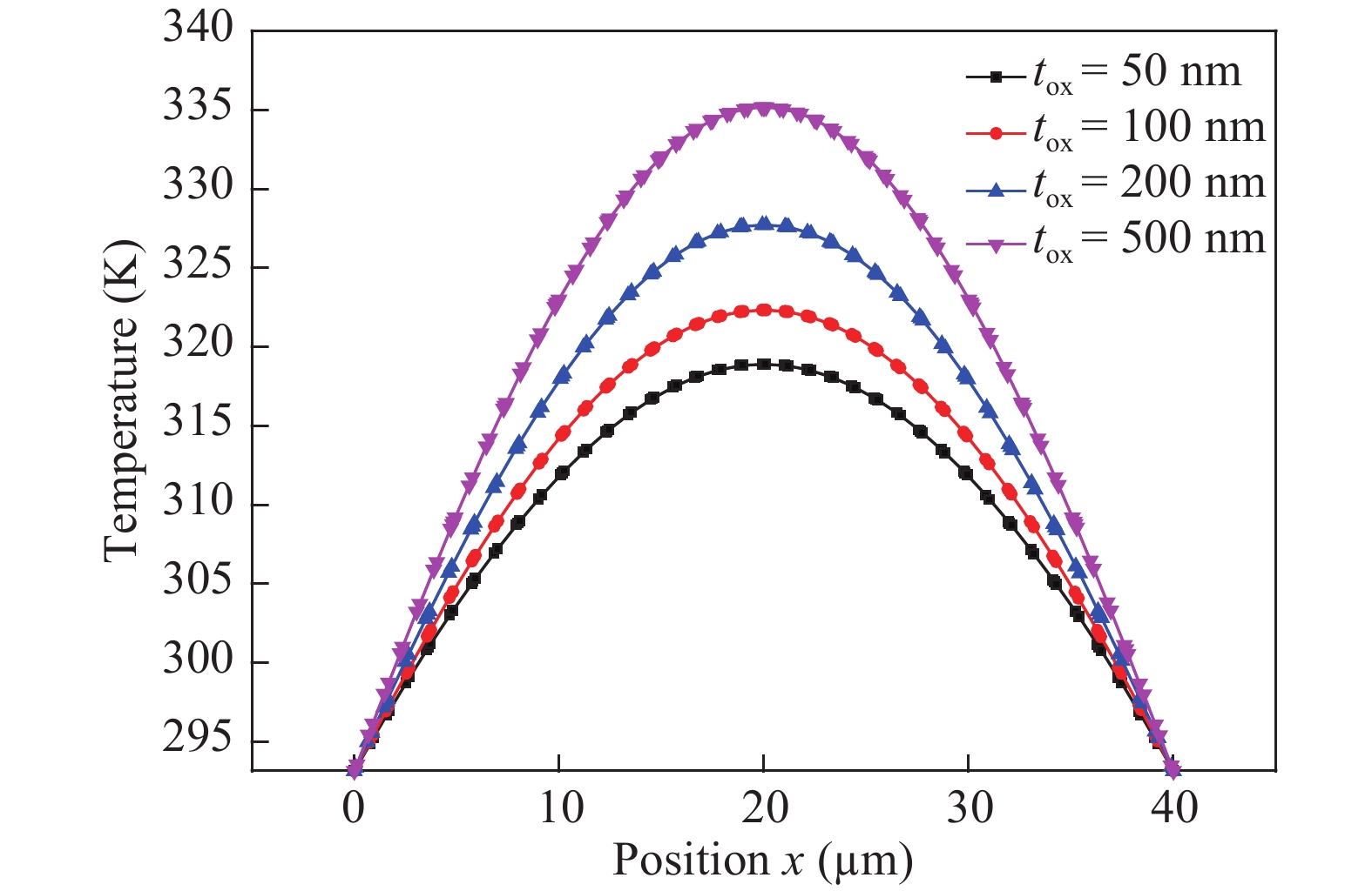
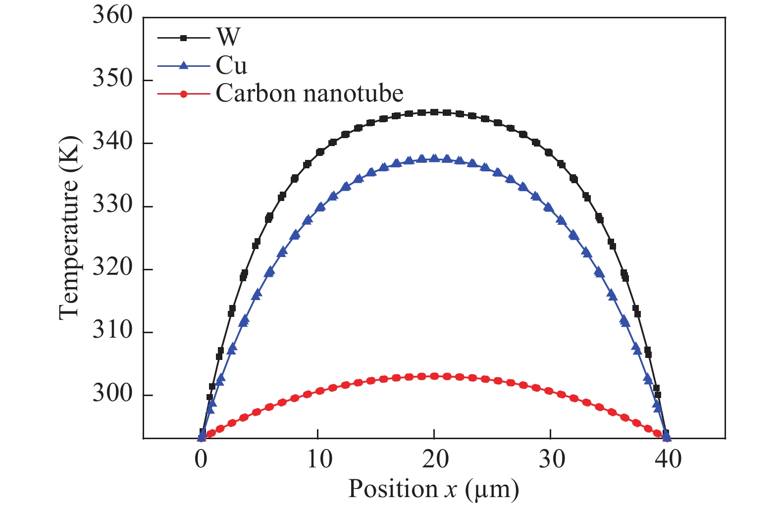
This paper presents a blended analytical electrical–thermal model for steady state thermal analysis of through-silicon-via (TSV) in three-dimensional (3D) integrated circuits. The proposed analytical model is validated by the commercial FEM tool—COMSOL. The comparison between the results of the proposed analytical formulas and COMSOL shows that the proposed formulas have very high accuracy with a maximum error of 0.1%. Based on the analytical model, the temperature performance of TSV is studied. Design guide lines of TSV are also given as: (1) the radius of the TSV increases, the resistance decreases and the temperature can be increased; (2) the thicker the dielectric layer, the higher the temperature; (3) compared with carbon nanotube, the Cu enlarges the temperature by 34 K, and the W case enlarges the temperature by 41 K.

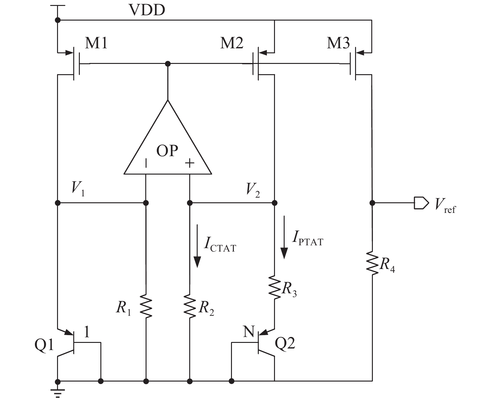
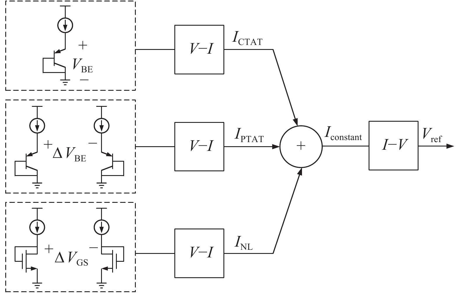
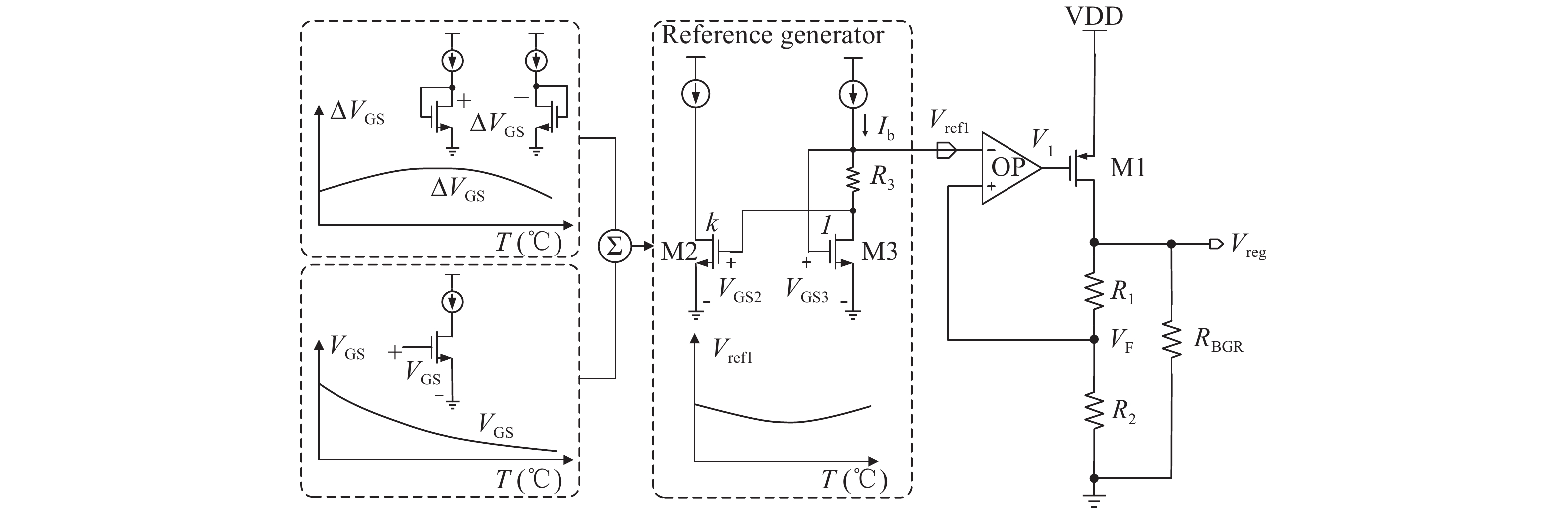
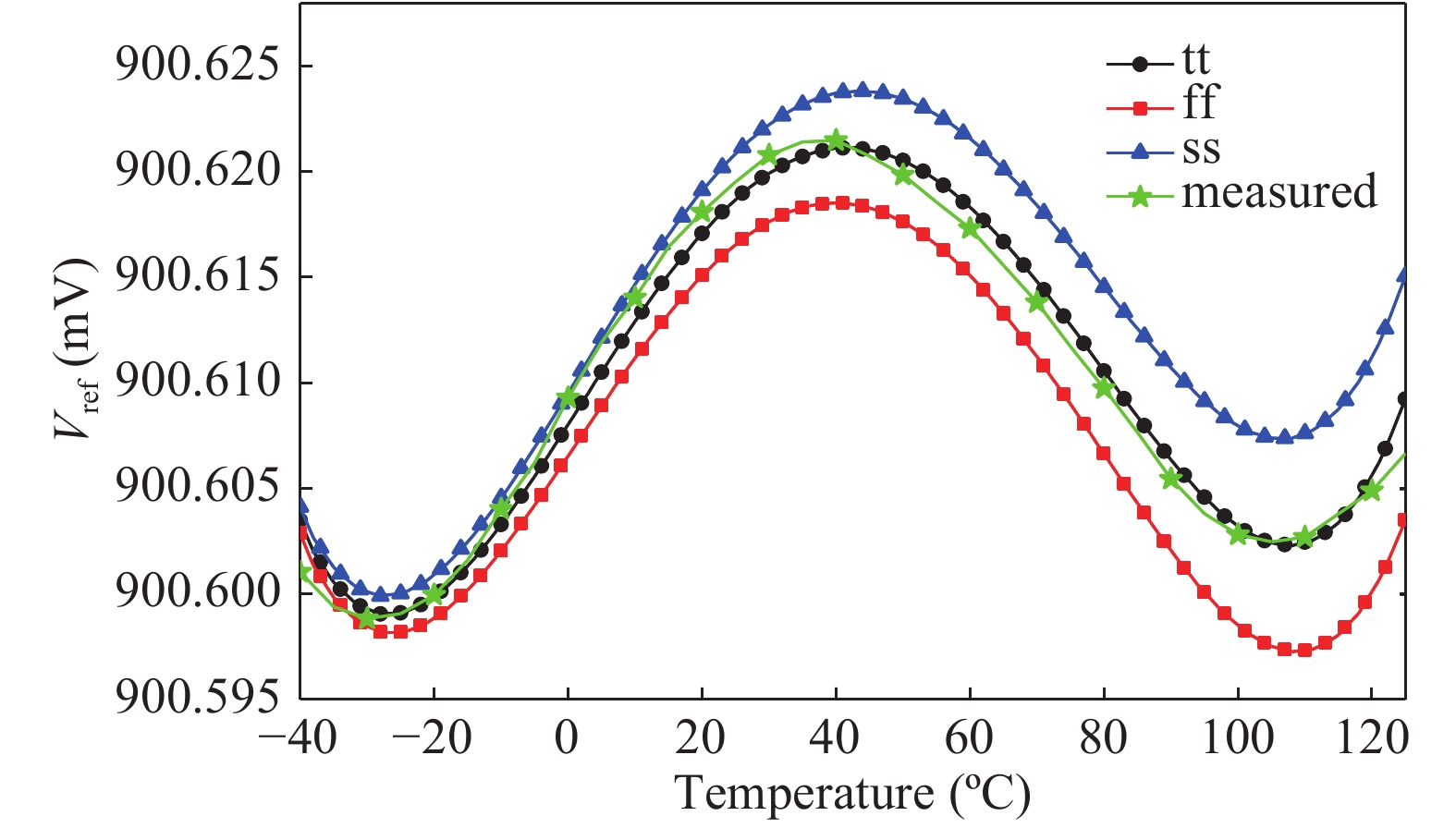
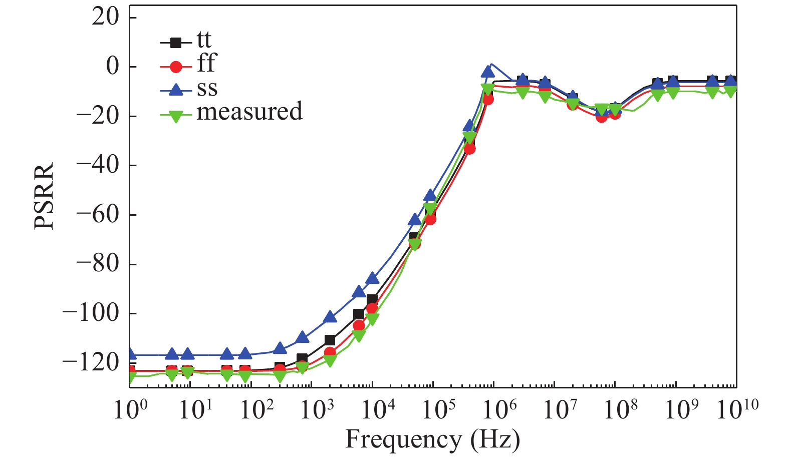
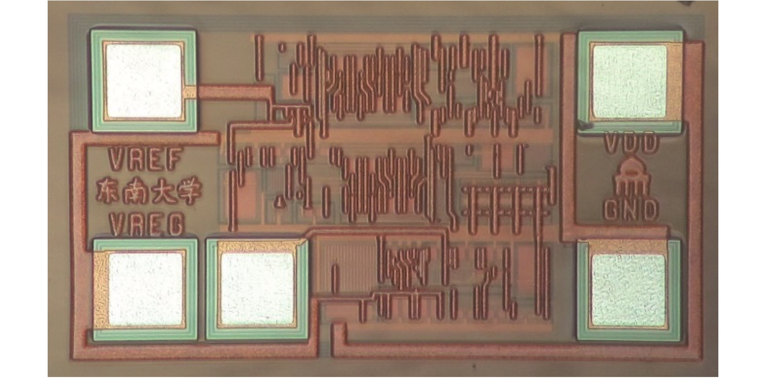
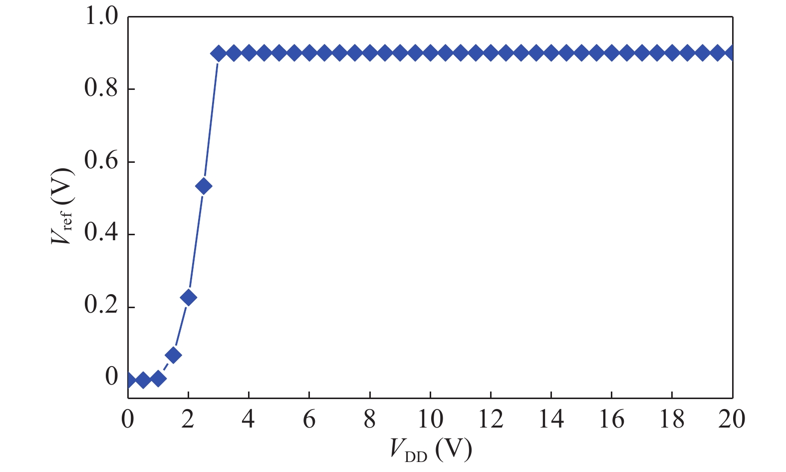
A high-order curvature-compensated CMOS bandgap reference (BGR) topology with a low temperature coefficient (TC) over a wide temperature range and a high power supply reject ratio (PSRR) is presented. High-order correction is realized by incorporating a nonlinear current INL, which is generated by ∆VGS across resistor into current generated by a conventional first-order current-mode BGR circuit. In order to achieve a high PSRR over a broad frequency range, a voltage pre-regulating technique is applied. The circuit was implemented in CSMC 0.5 μm 600 V BCD process. The experimental results indicate that the proposed topology achieves TC of 0.19 ppm/°C over the temperature range of 165 °C (−40 to 125 °C), PSRR of −123 dB @ DC and −56 dB @ 100 kHz. In addition, it achieves a line regulation performance of 0.017%/V in the supply range of 2.8–20 V.