Issue Browser
Volume 40, Issue 10,
Oct 2019


J. Semicond.
2019, 40(10): 101301 doi: 10.1088/1674-4926/40/10/101301

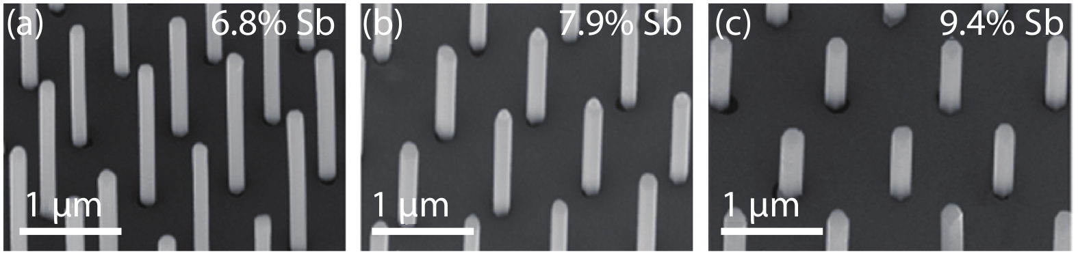
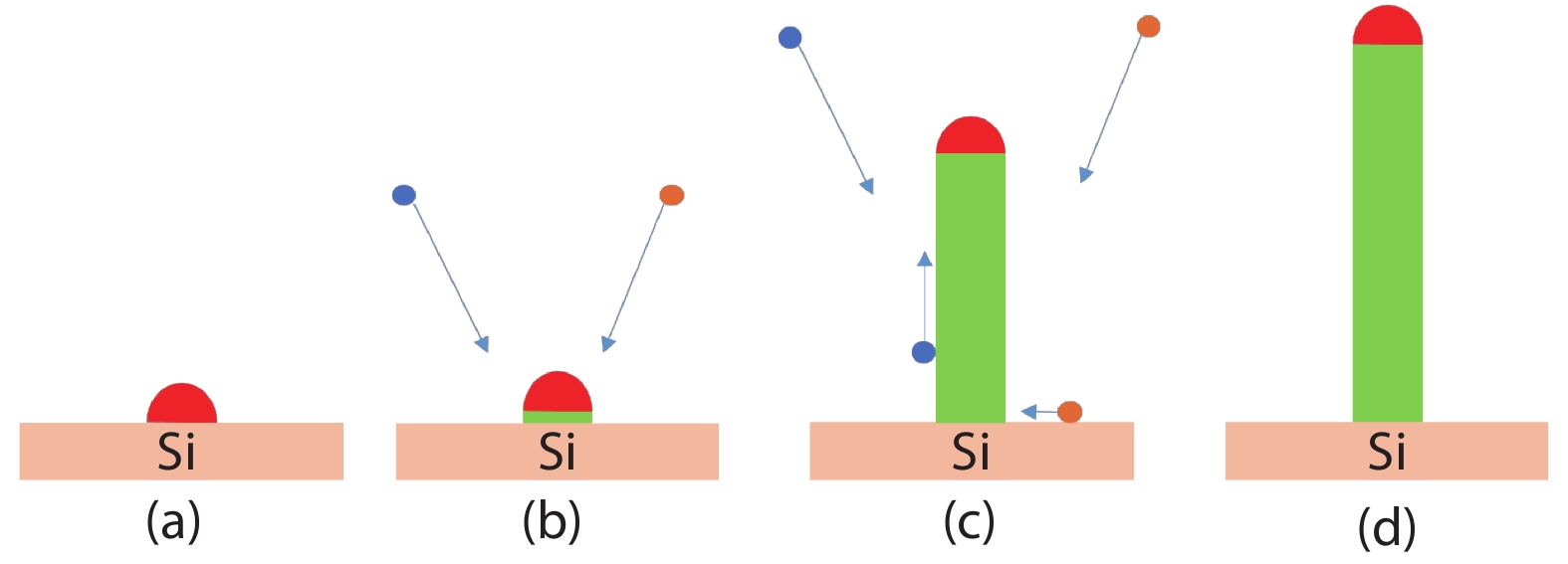
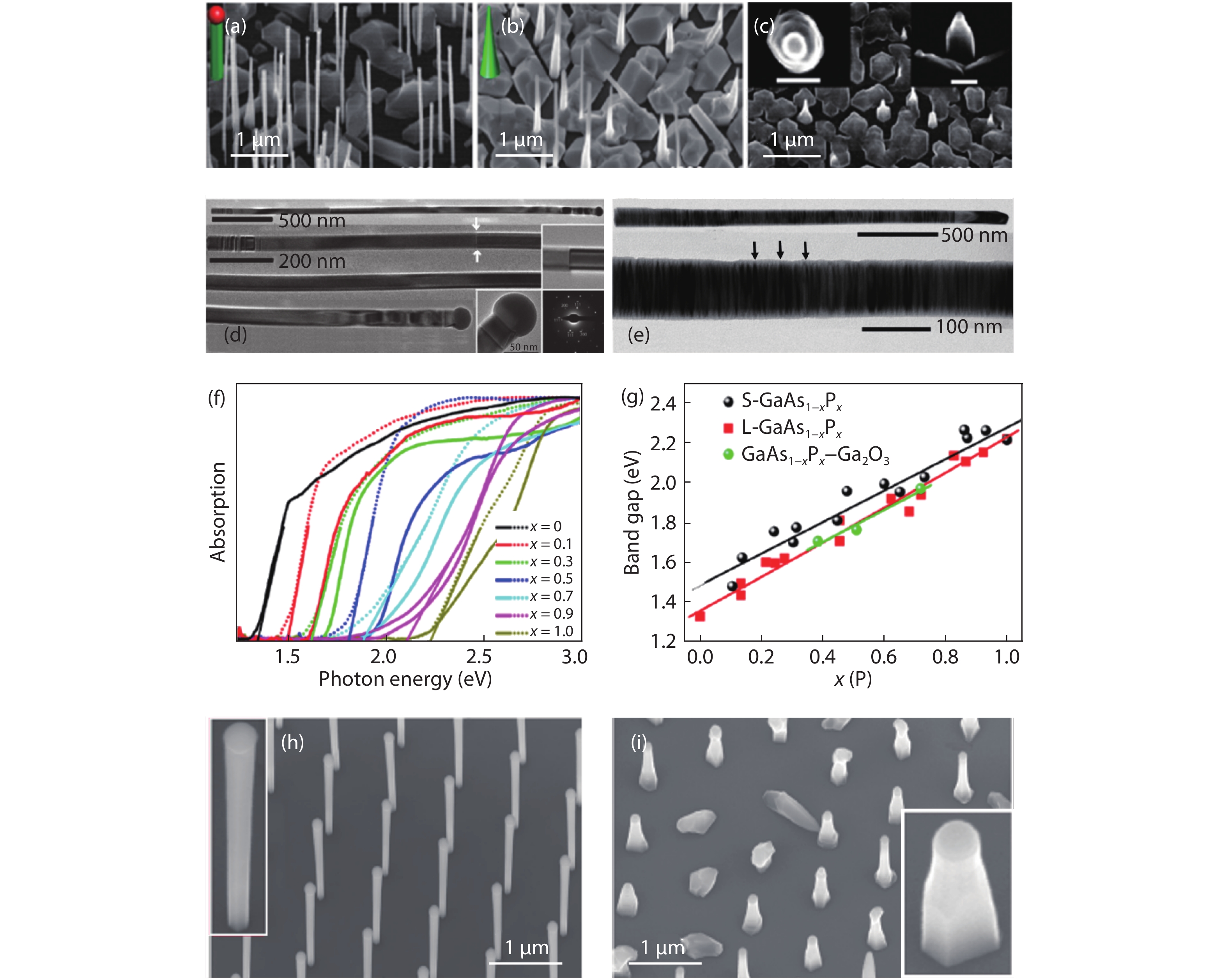
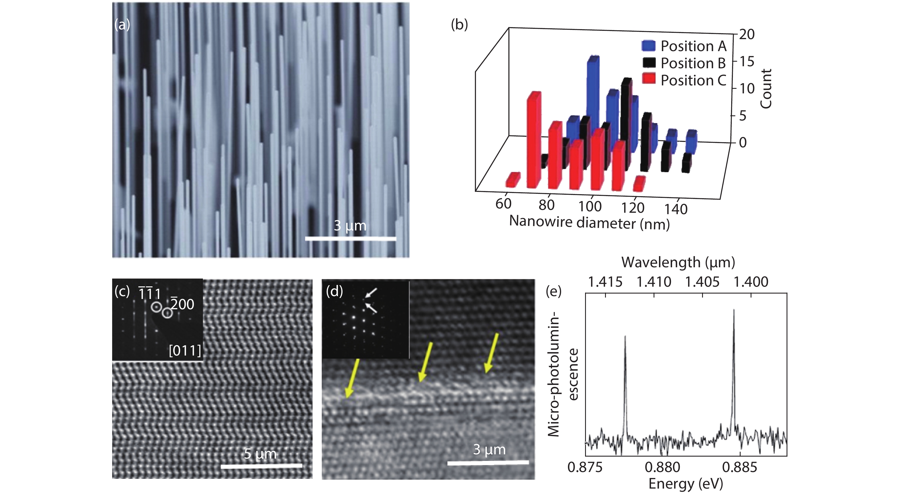
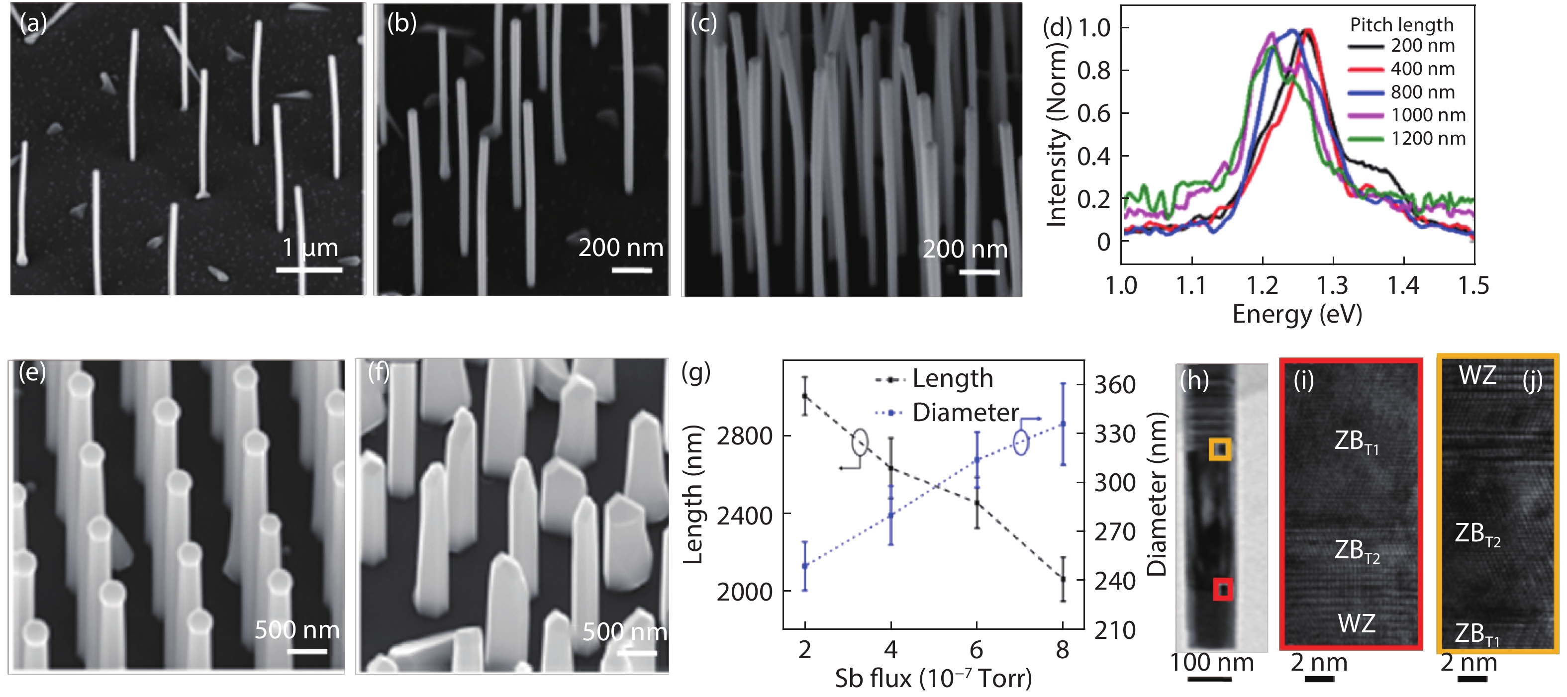
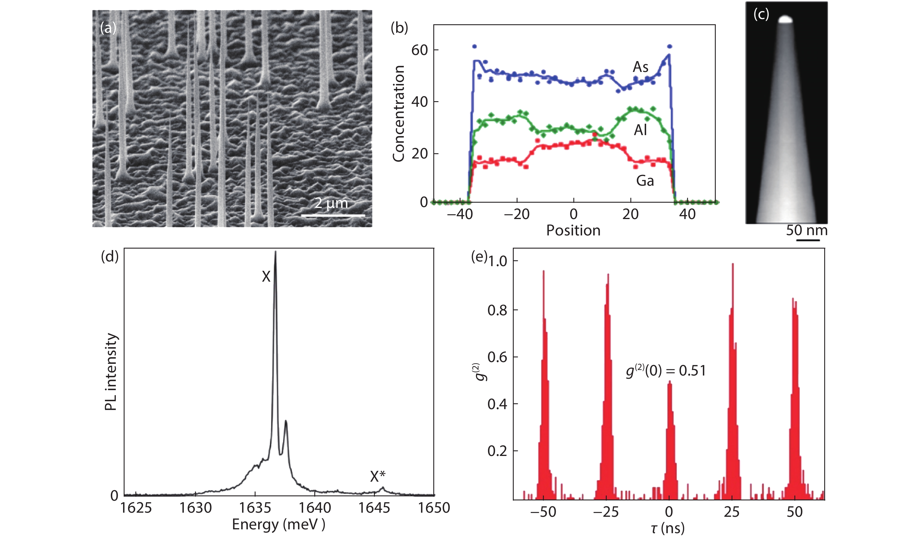
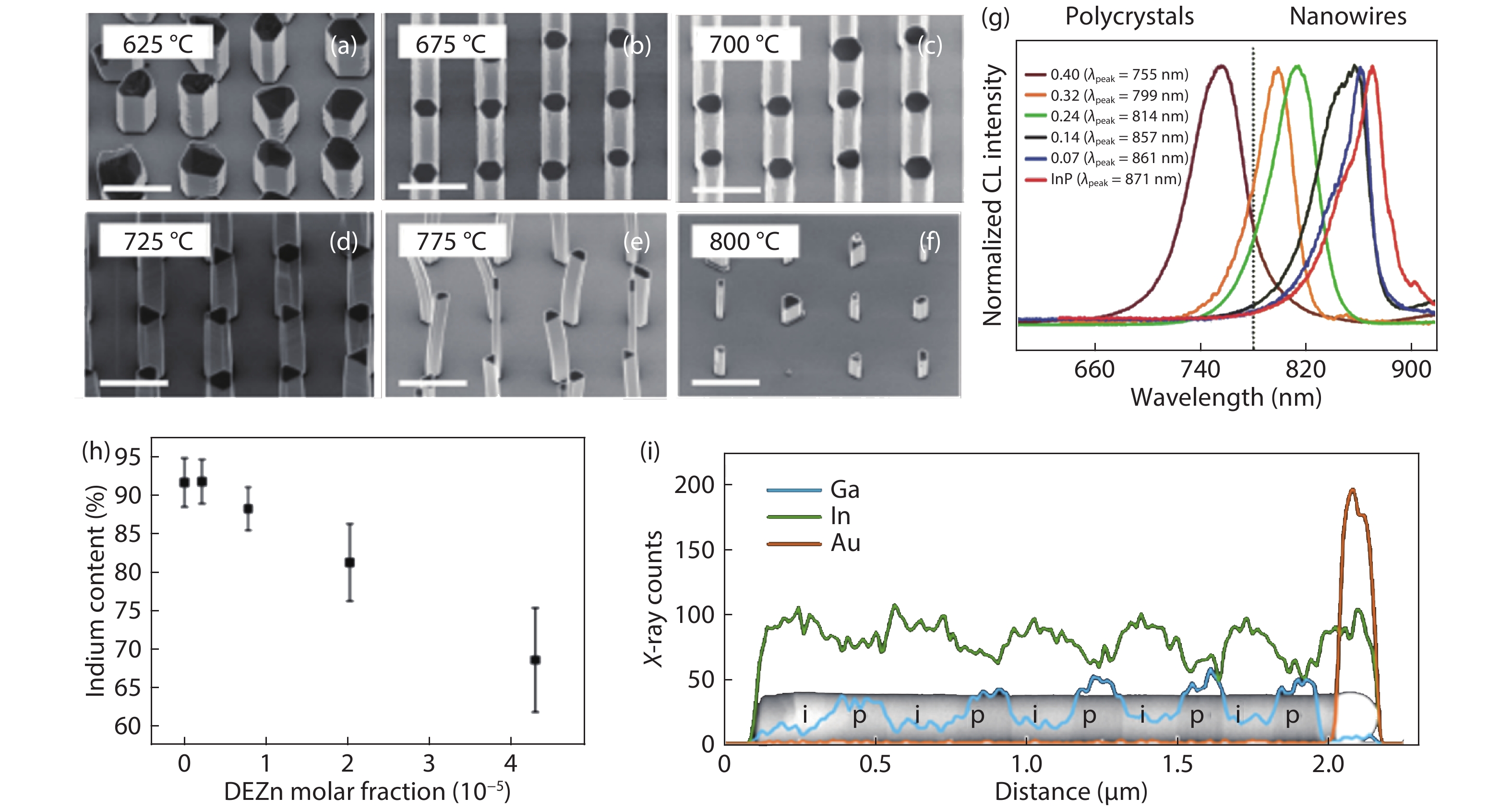
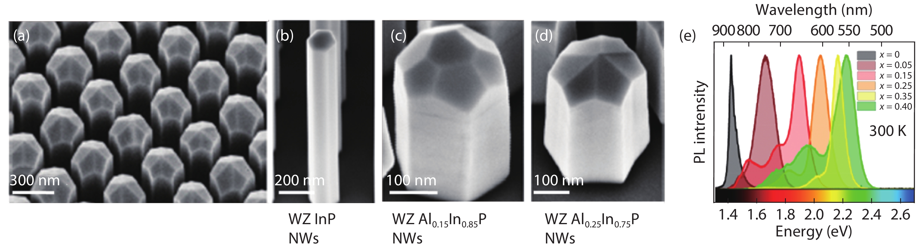
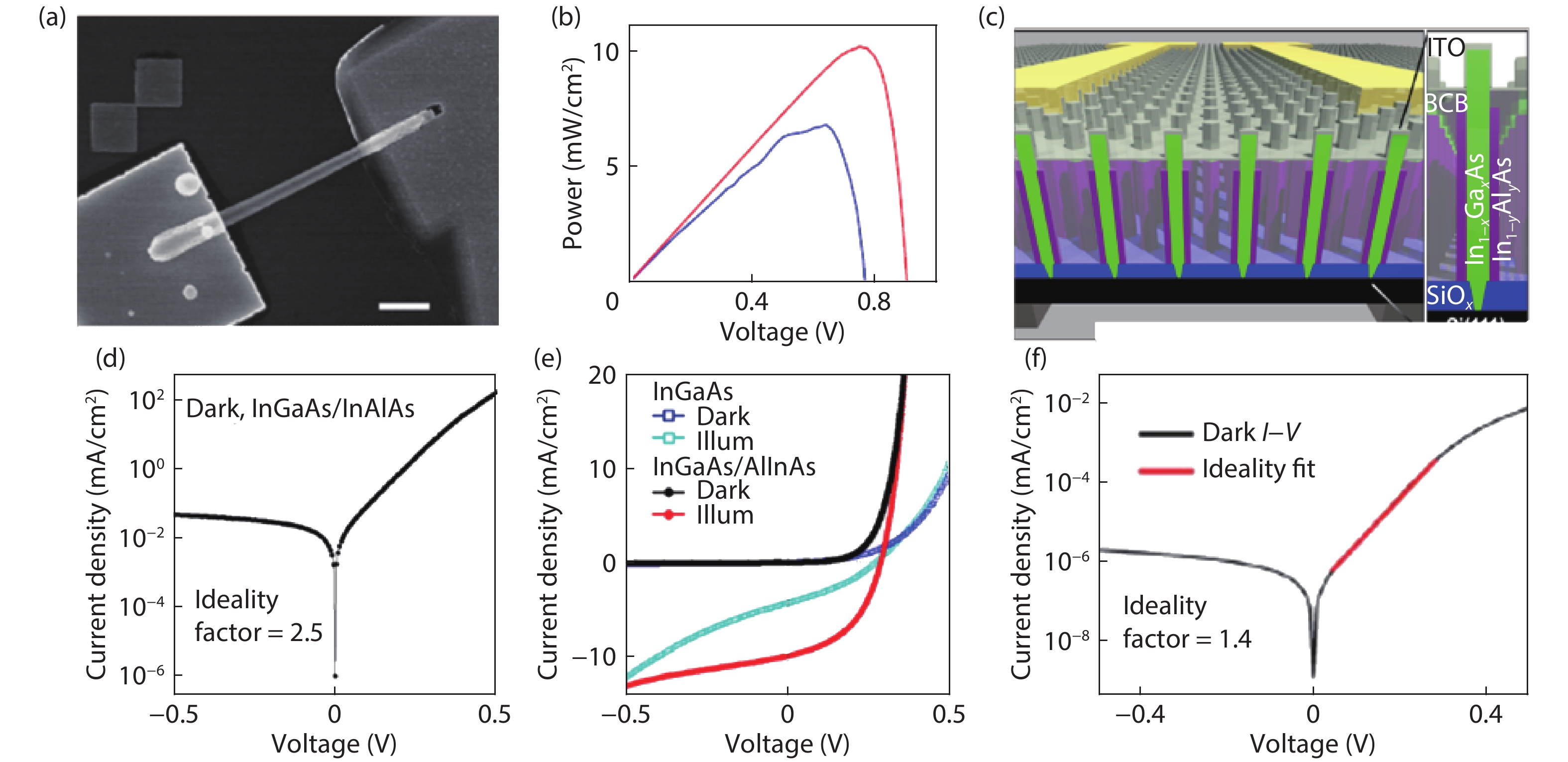
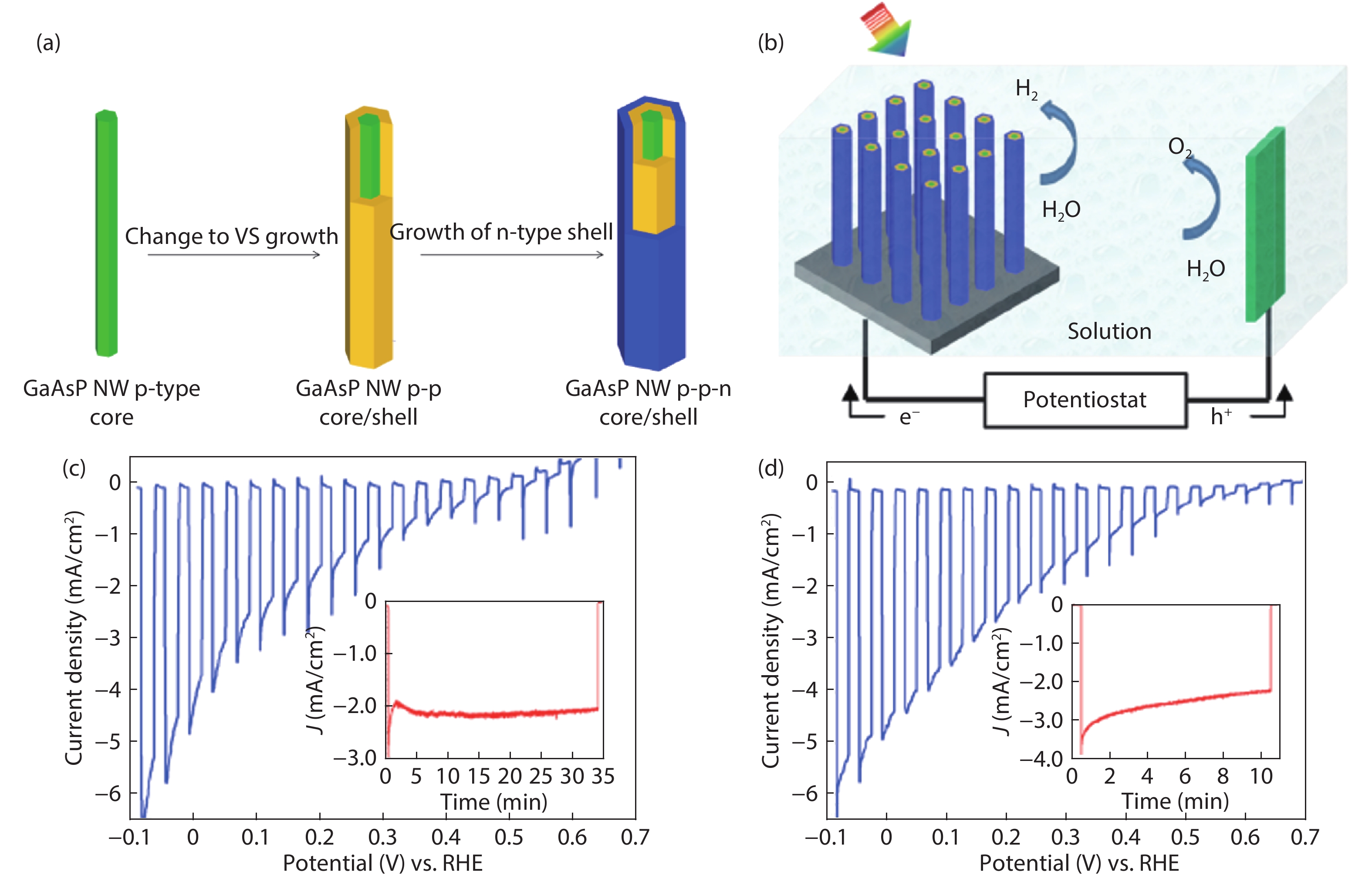
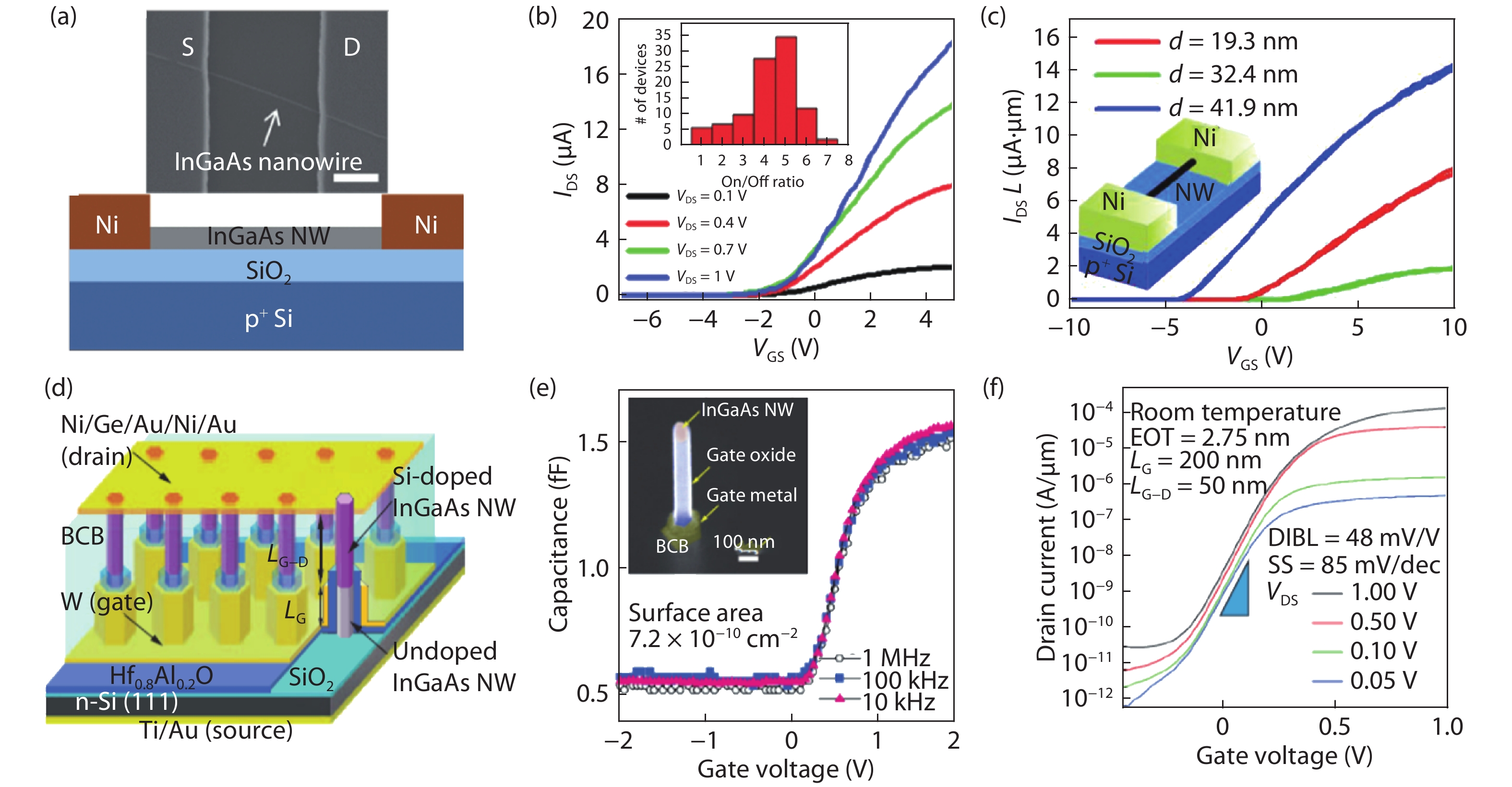
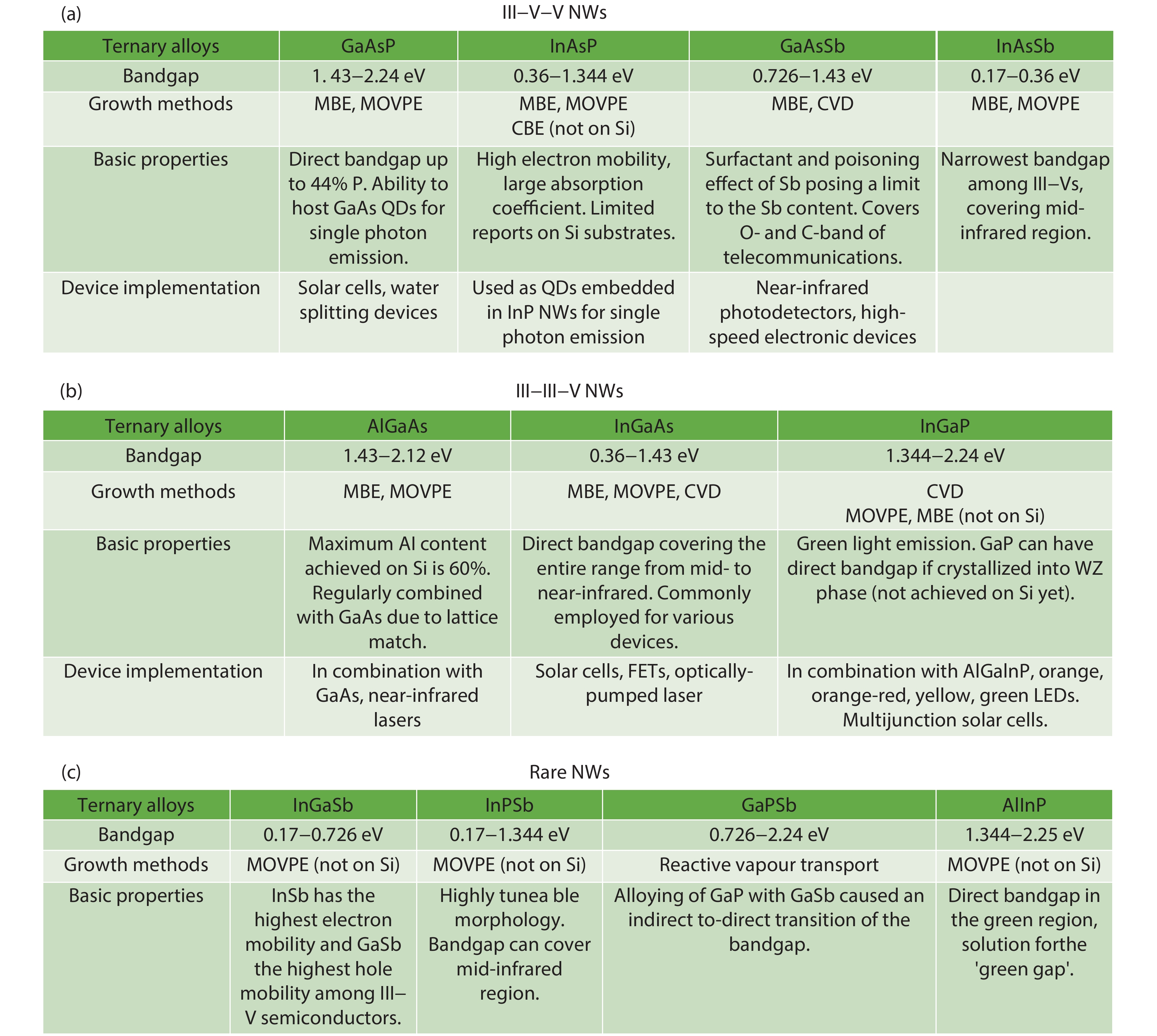
Over the past decades, the progress in the growth of materials which can be applied to cutting-edge technologies in the field of electronics, optoelectronics and energy harvesting has been remarkable. Among the various materials, group III–V semiconductors are of particular interest and have been widely investigated due to their excellent optical properties and high carrier mobility. However, the integration of III–V structures as light sources and numerous other optical components on Si, which is the foundation for most optoelectronic and electronic integrated circuits, has been hindered by the large lattice mismatch between these compounds. This mismatch results in substantial amounts of strain and degradation of the performance of the devices. Nanowires (NWs) are unique nanostructures that induce elastic strain relaxation, allowing for the monolithic integration of III–V semiconductors on the cheap and mature Si platform. A technique that ensures flexibility and freedom in the design of NW structures is the growth of ternary III–V NWs, which offer a tuneable frame of optical characteristics, merely by adjusting their nominal composition. In this review, we will focus on the recent progress in the growth of ternary III–V NWs on Si substrates. After analysing the growth mechanisms that are being employed and describing the effect of strain in the NW growth, we will thoroughly inspect the available literature and present the growth methods, characterization and optical measurements of each of the III–V ternary alloys that have been demonstrated. The different properties and special treatments required for each of these material platforms are also discussed. Moreover, we will present the results from the works on device fabrication, including lasers, solar cells, water splitting devices, photodetectors and FETs, where ternary III–V NWs were used as building blocks. Through the current paper, we exhibit the up-to-date state in this field of research and summarize the important accomplishments of the past few years.


J. Semicond.
2019, 40(10): 101302 doi: 10.1088/1674-4926/40/10/101302

In the past few decades, numerous high-performance silicon (Si) photonic devices have been demonstrated. Si, as a photonic platform, has received renewed interest in recent years. Efficient Si-based III–V quantum-dot (QDs) lasers have long been a goal for semiconductor scientists because of the incomparable optical properties of III–V compounds. Although the material dissimilarity between III–V material and Si hindered the development of monolithic integrations for over 30 years, considerable breakthroughs happened in the 2000s. In this paper, we review recent progress in the epitaxial growth of various III–V QD lasers on both offcut Si substrate and on-axis Si (001) substrate. In addition, the fundamental challenges in monolithic growth will be explained together with the superior characteristics of QDs.


J. Semicond.
2019, 40(10): 101303 doi: 10.1088/1674-4926/40/10/101303

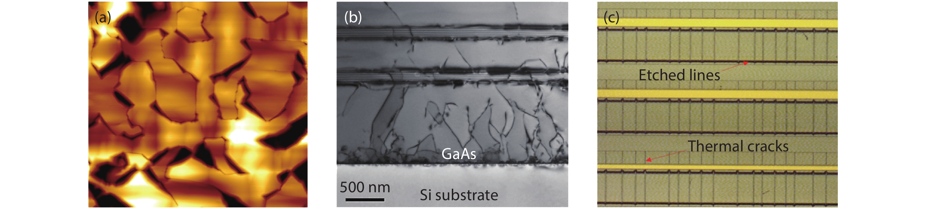
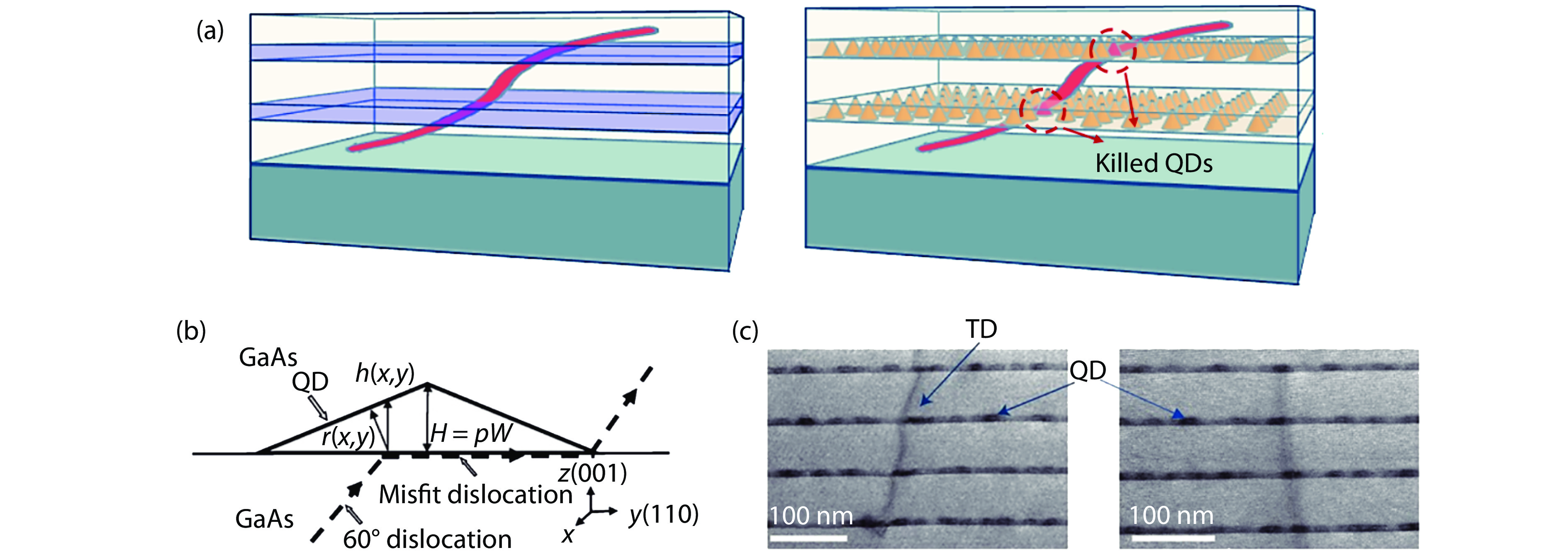
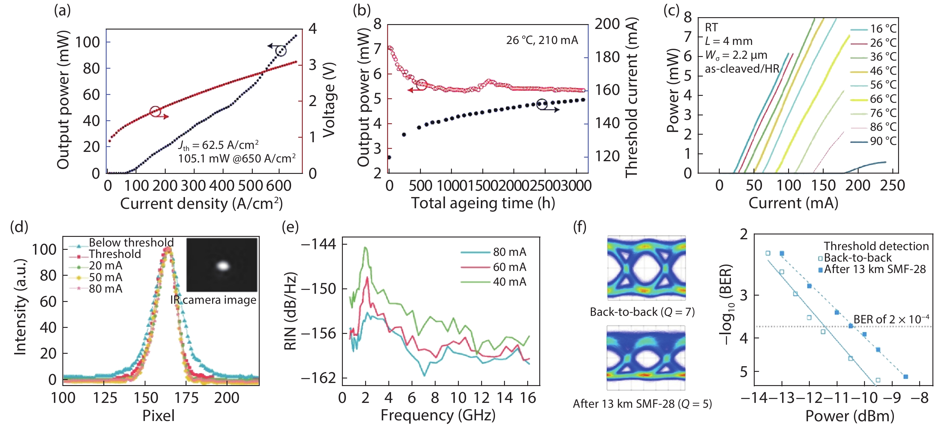
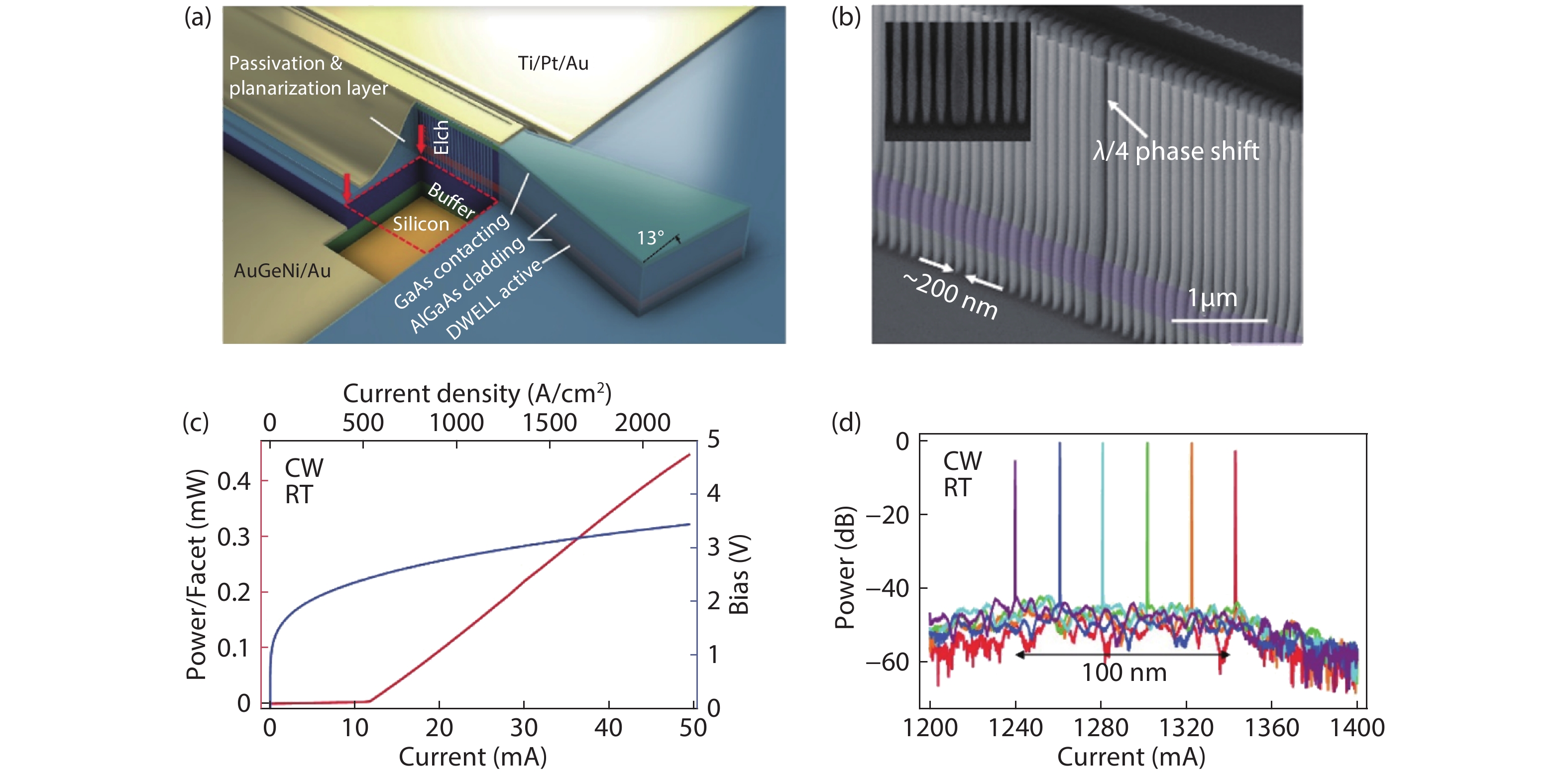
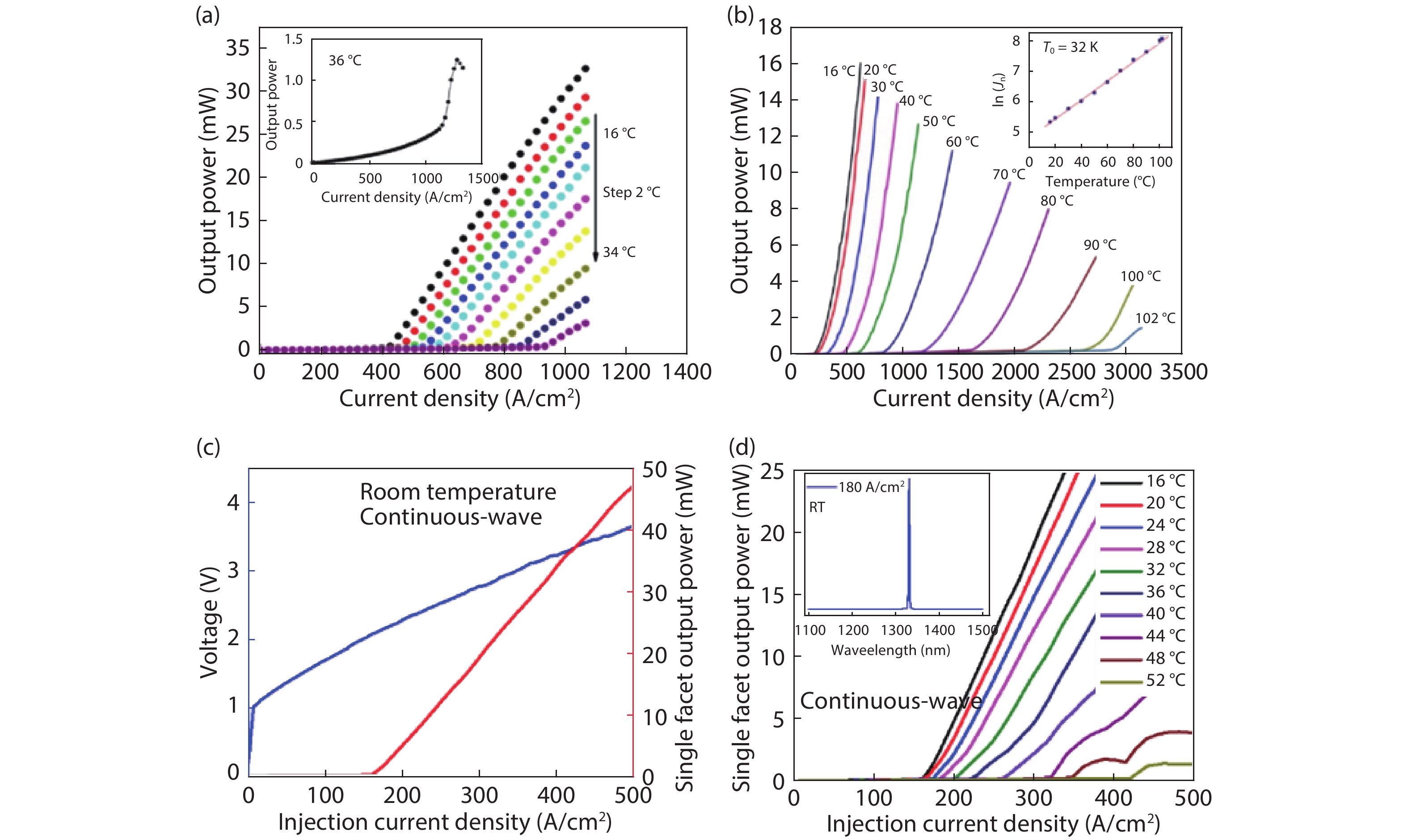
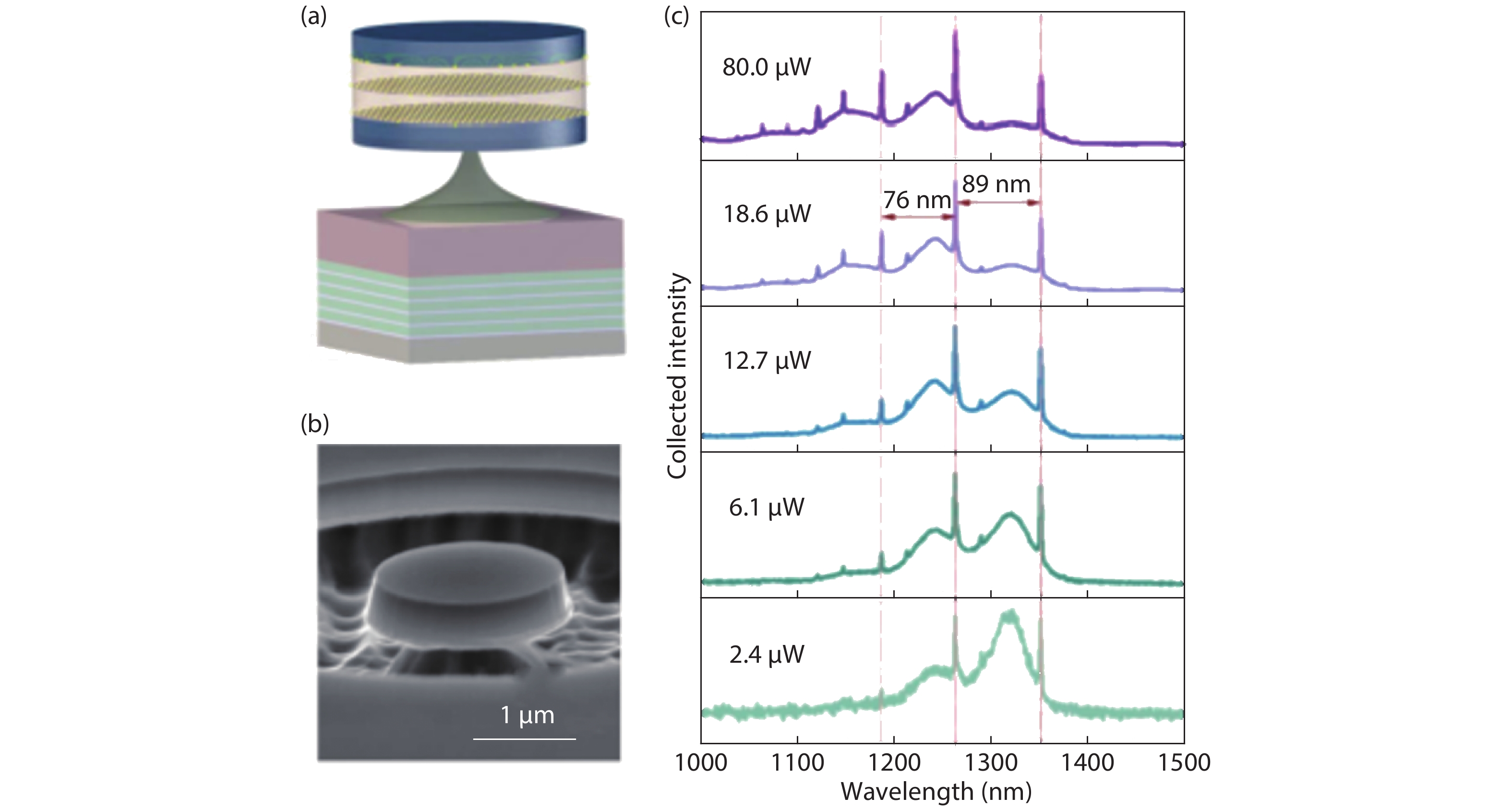
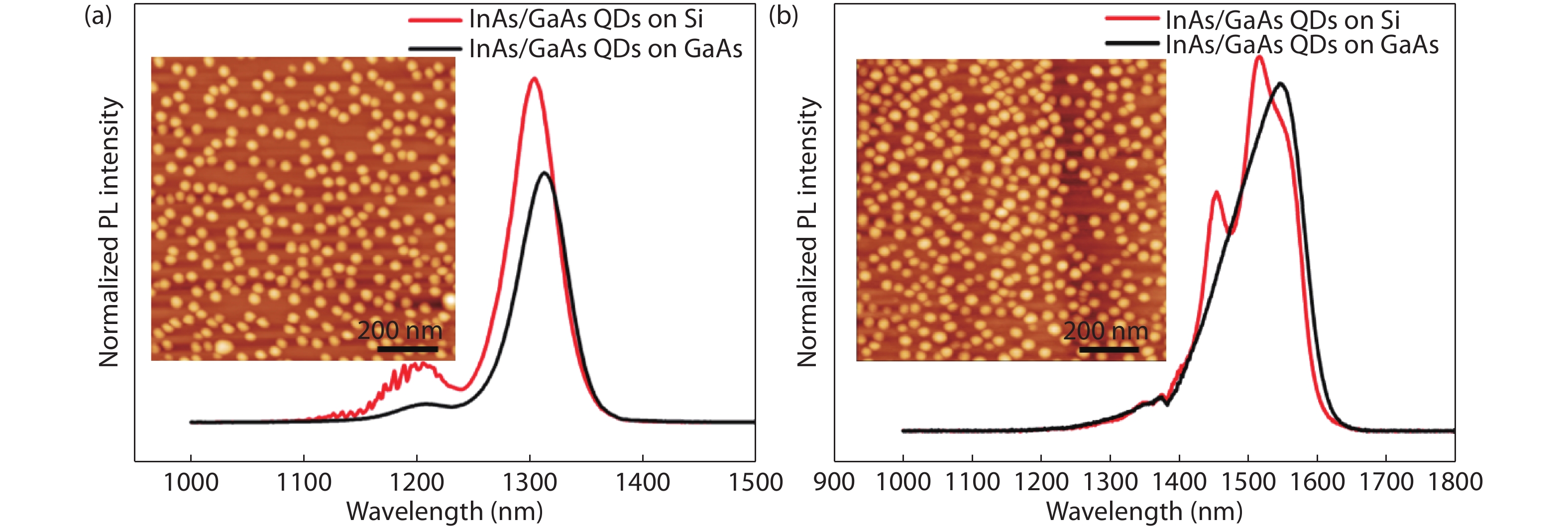
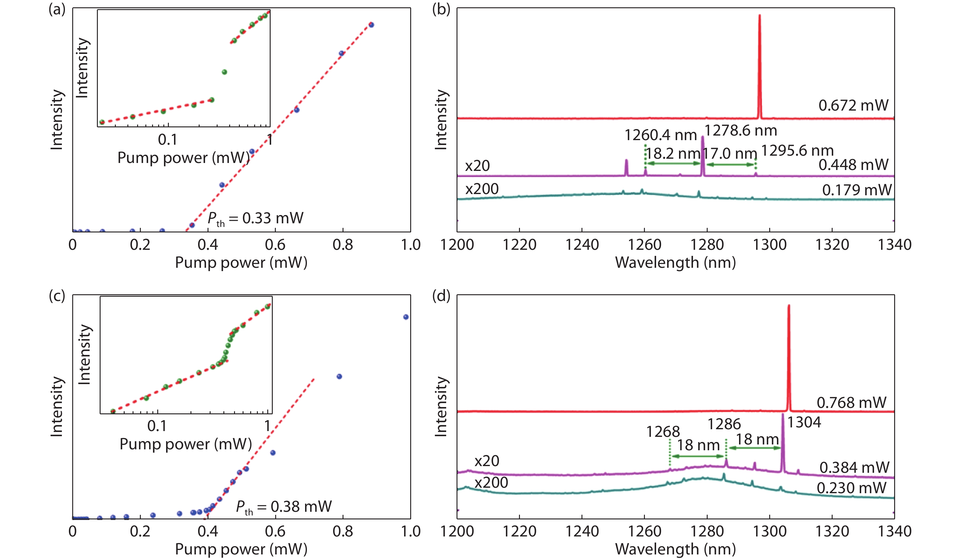
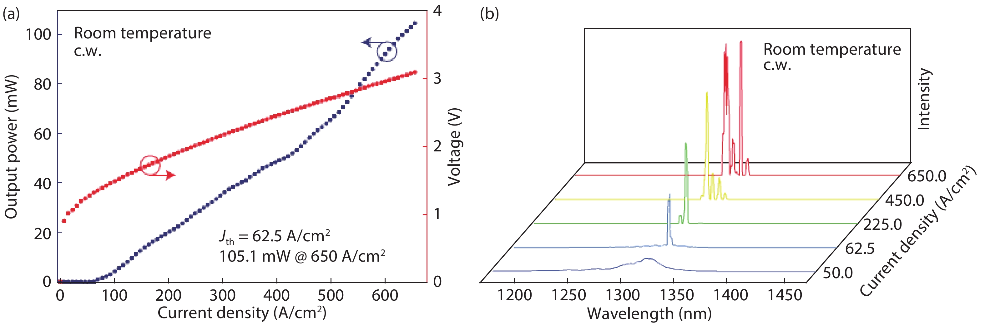
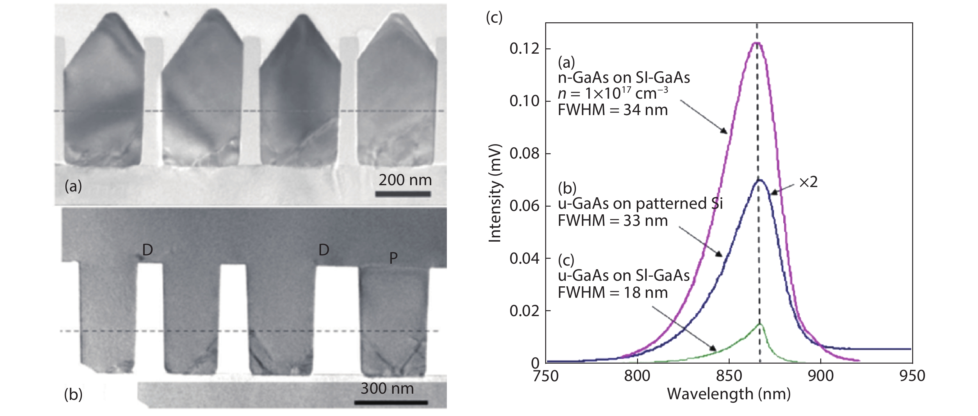
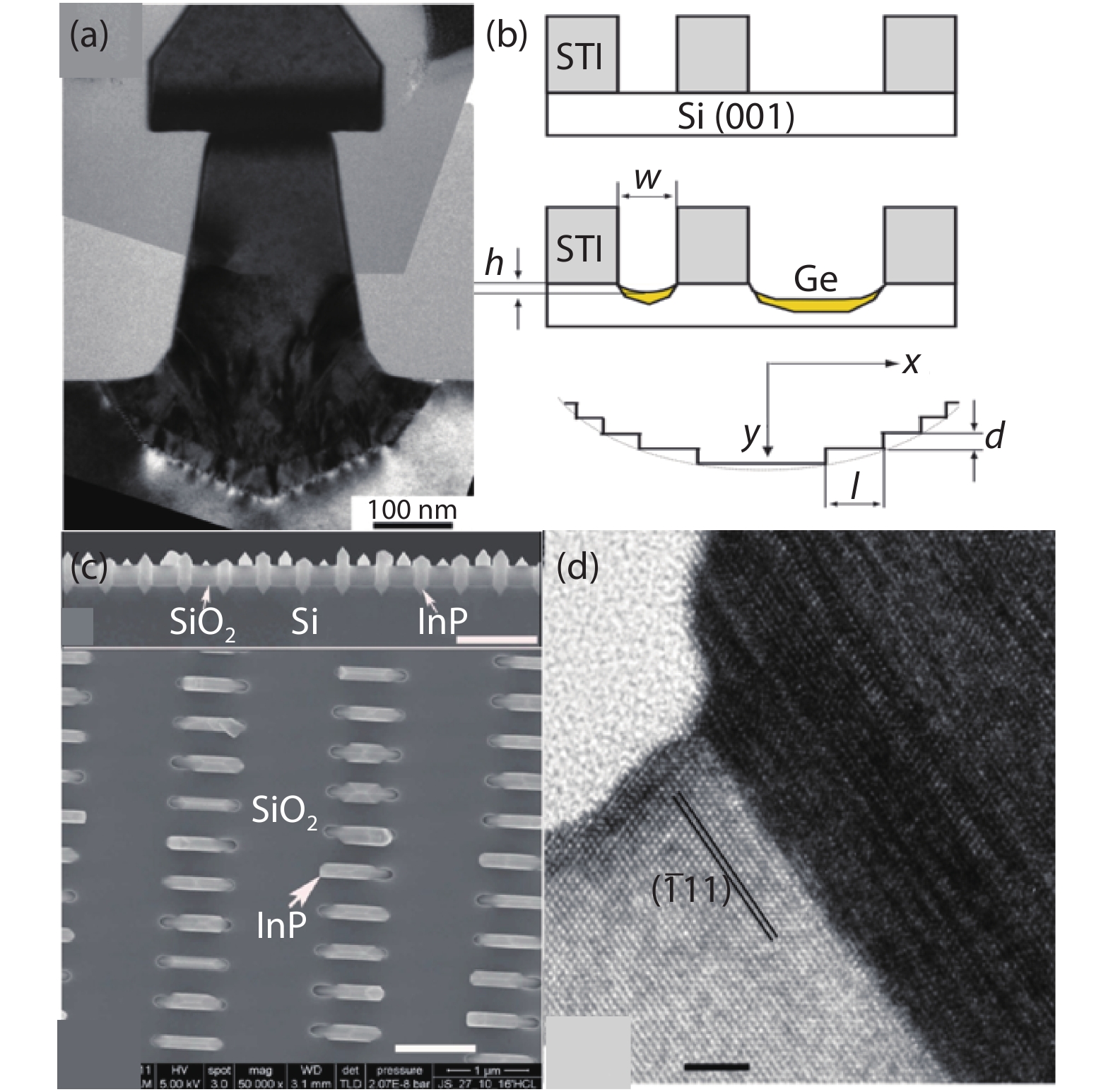
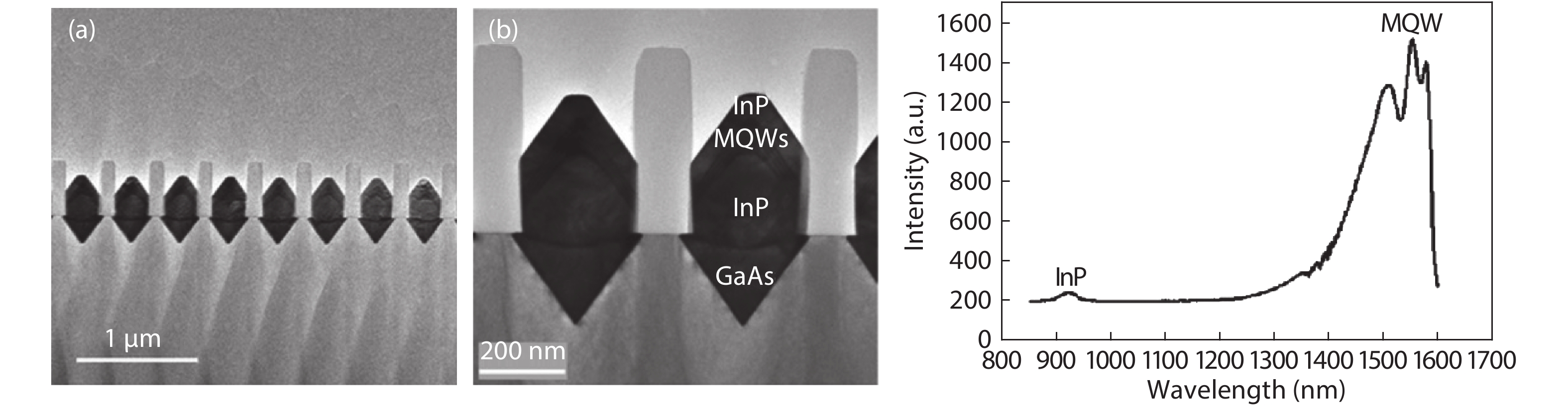
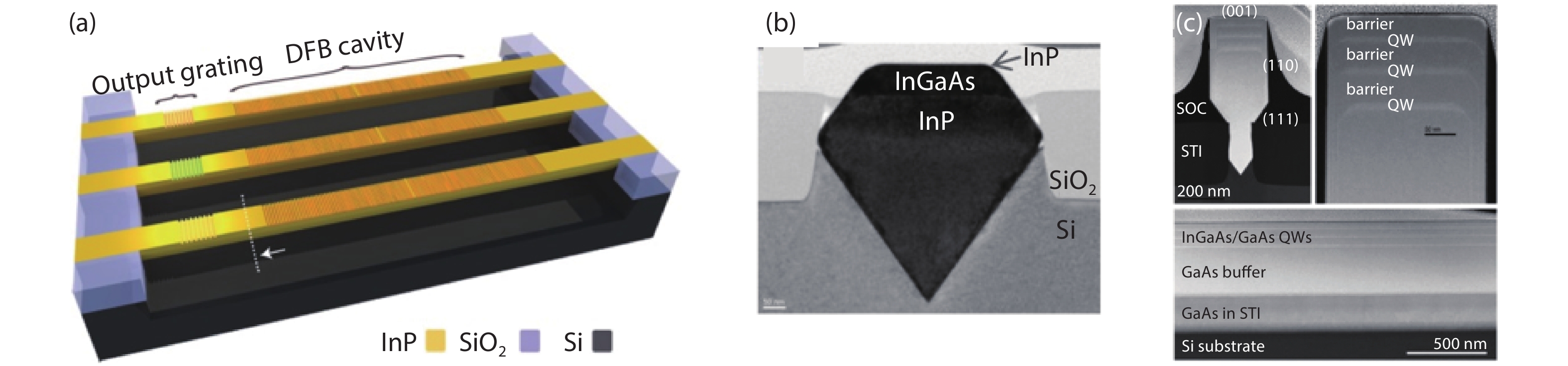
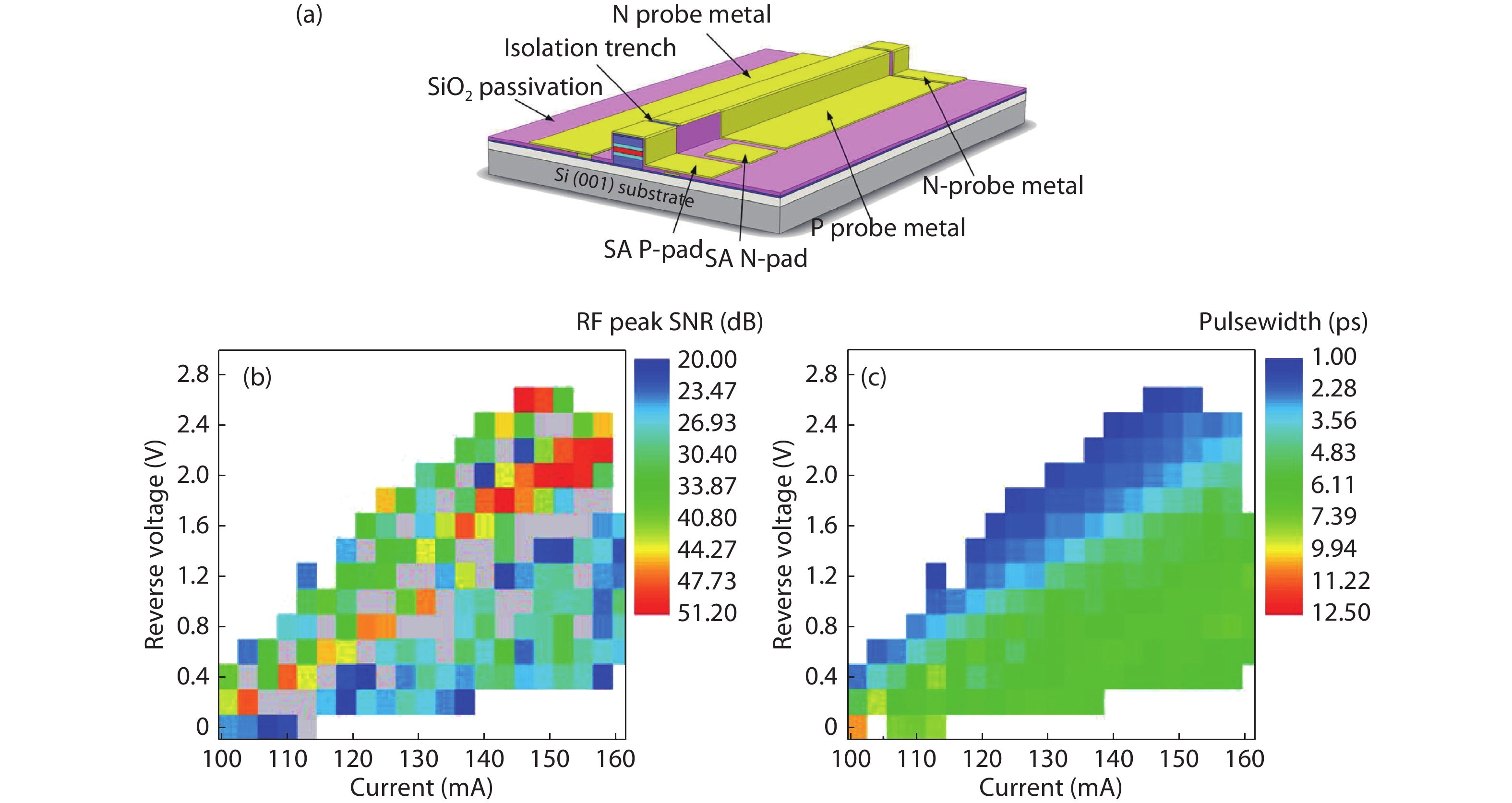
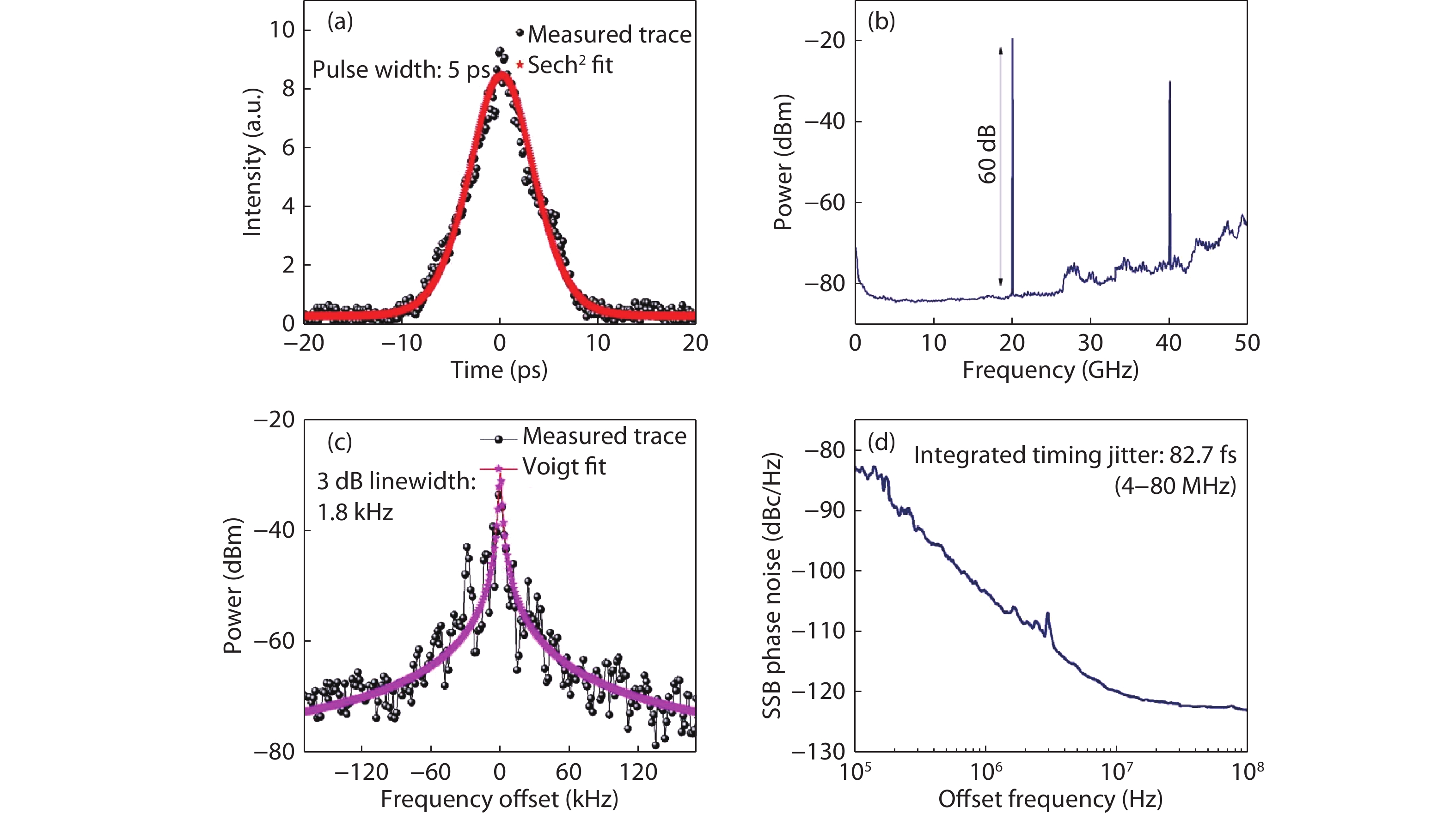
Direct epitaxial growth III–V quantum dot (QD) structures on CMOS-compatible silicon substrates is considered as one of the most promising approaches to achieve low-cost and high-yield Si-based lasers for silicon photonic integration. However, epitaxial growth of III–V materials on Si encounters the following three major challenges: high density of threading dislocations, antiphase boundaries and thermal cracks, which significantly degrade the crystal quality and potential device performance. In this review, we will focus on some recent results related to InAs/GaAs quantum dot lasers on Si (001) substrates by III–V/IV hybrid epitaxial growth via (111)-faceted Si hollow structures. Moreover, by using the step-graded epitaxial growth process the emission wavelength of InAs QDs can be extended from O-band to C/L-band. High-performance InAs/GaAs QD micro-disk lasers with sub-milliwatts threshold on Si (001) substrates are fabricated and characterized. The above results pave a promising path towards the on-chip lasers for optical interconnect applications.


J. Semicond.
2019, 40(10): 101304 doi: 10.1088/1674-4926/40/10/101304

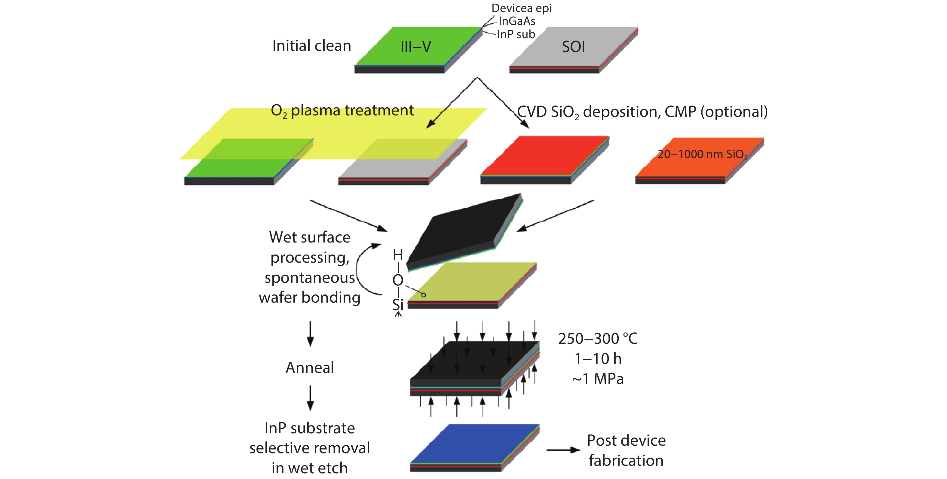
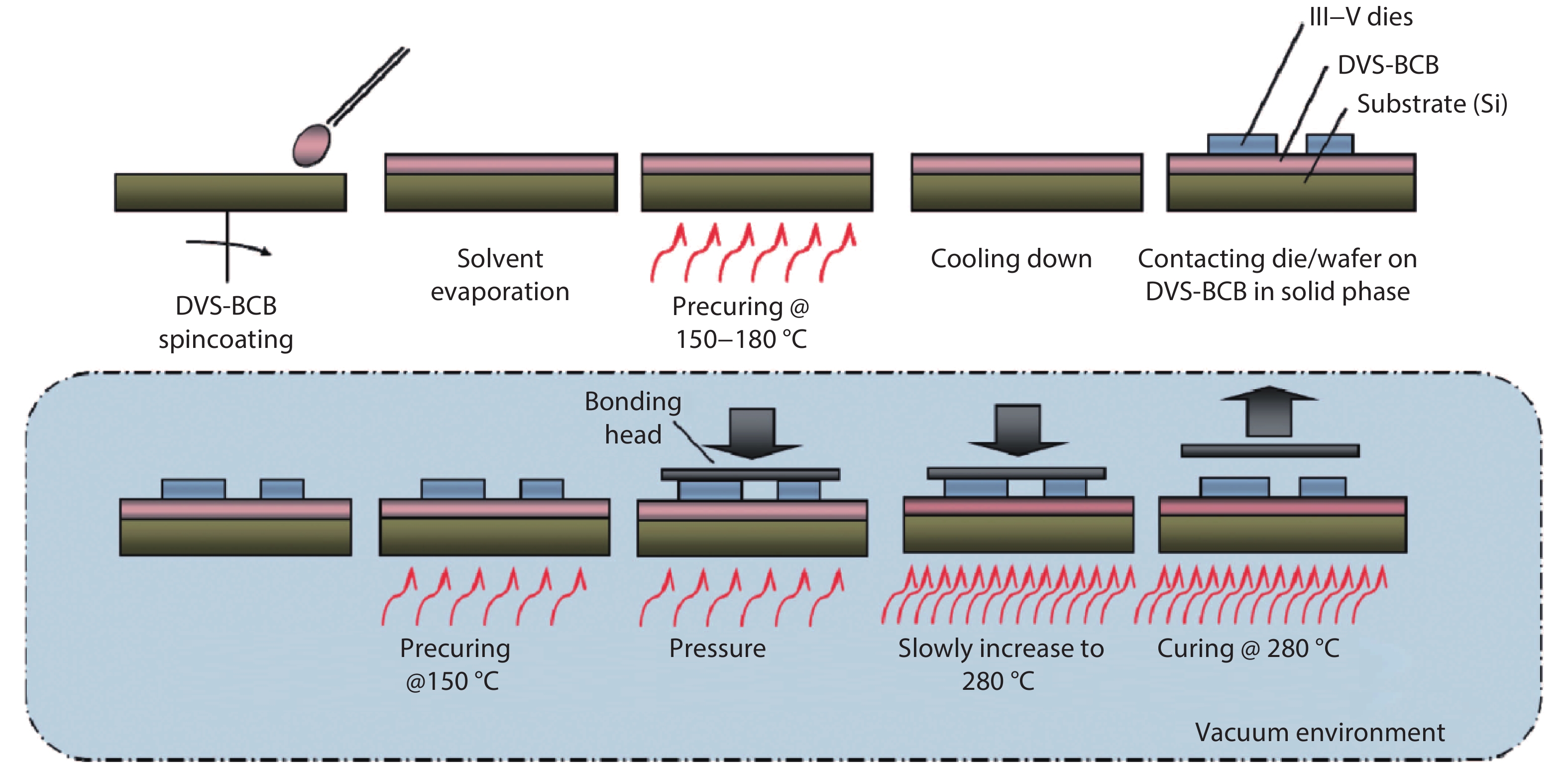
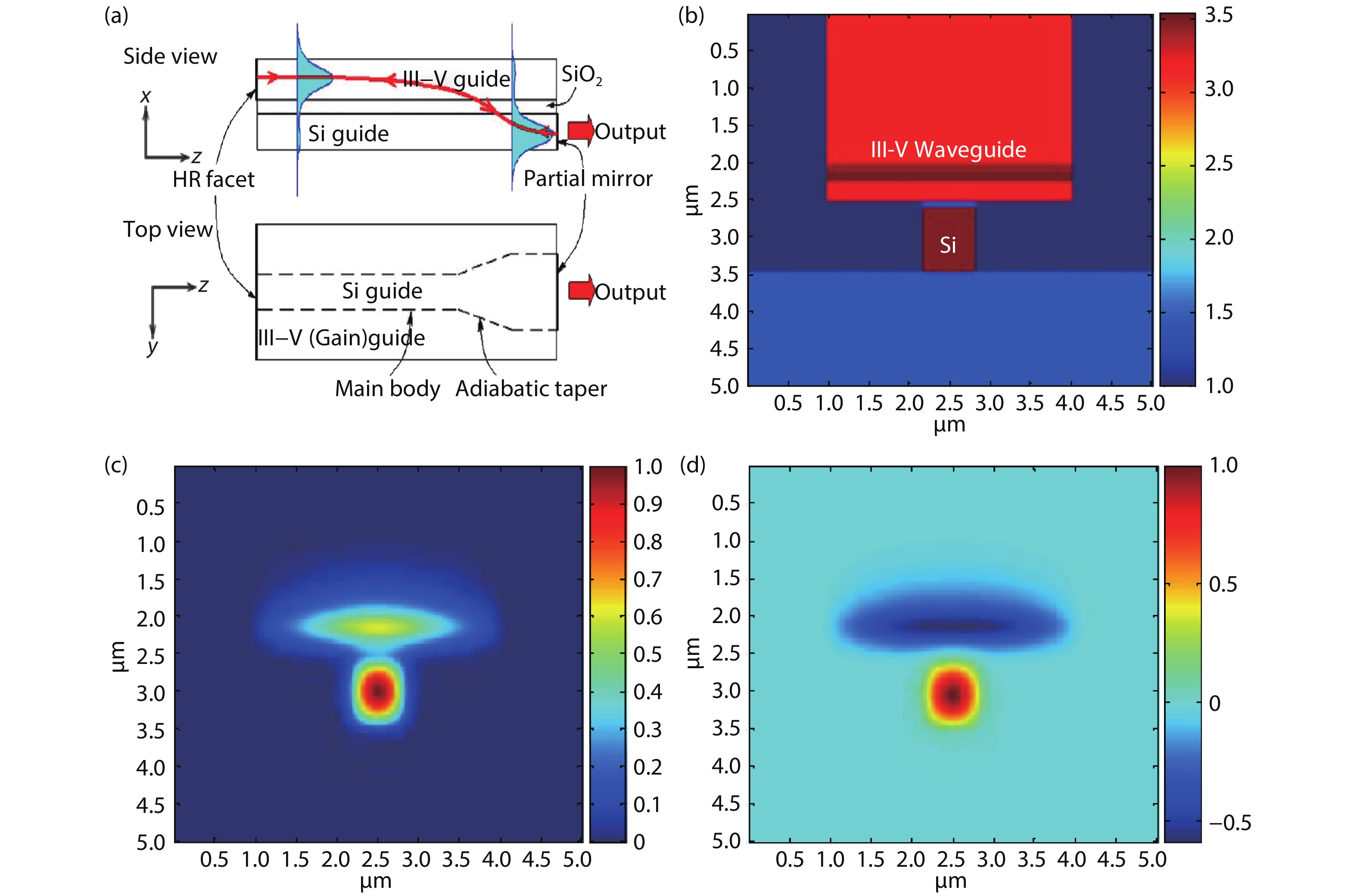
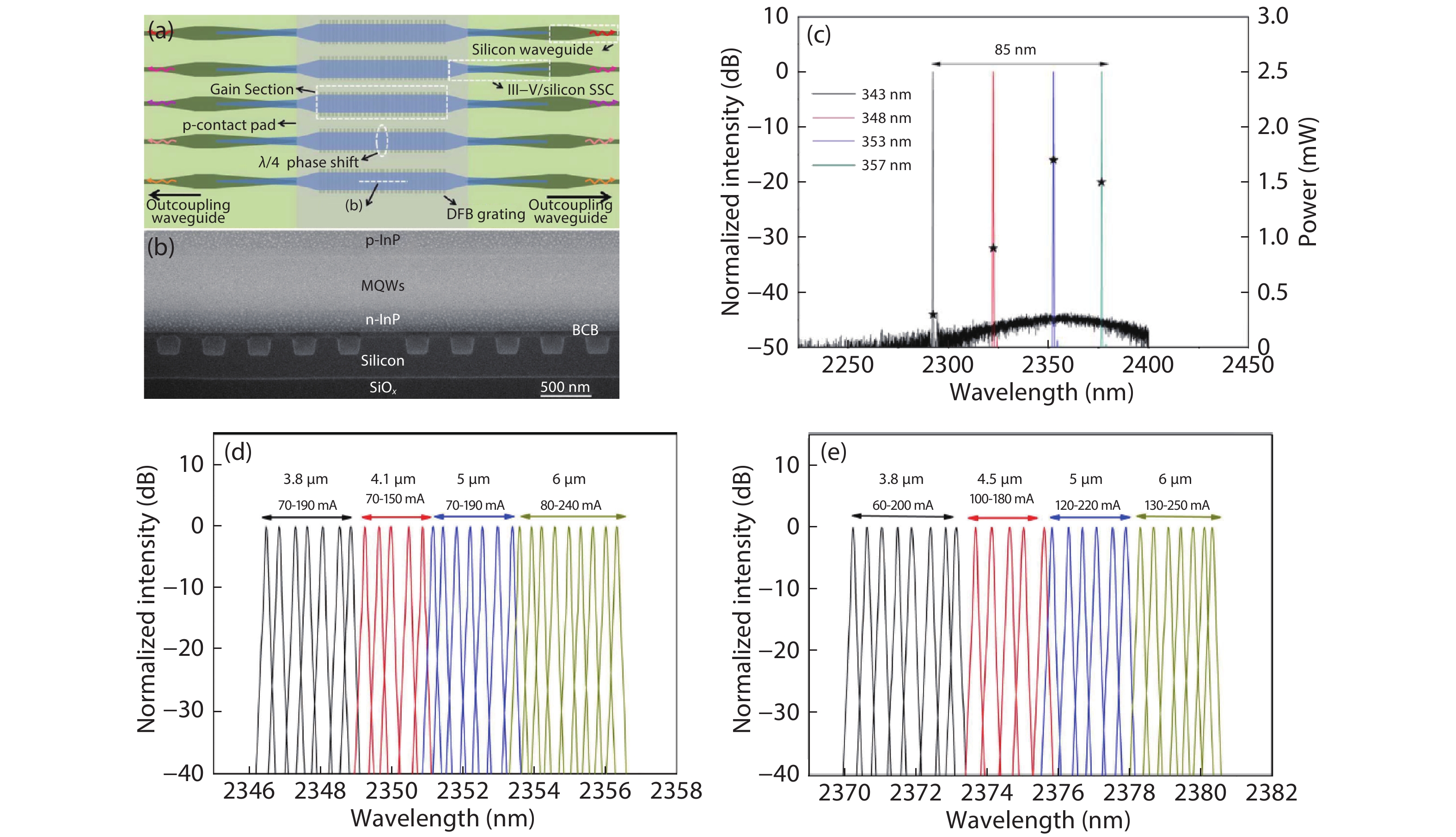
Due to the indirect bandgap nature, the widely used silicon CMOS is very inefficient at light emitting. The integration of silicon lasers is deemed as the ‘Mount Everest’ for the full take-up of Si photonics. The major challenge has been the materials dissimilarity caused impaired device performance. We present a brief overview of the recent advances of integrated III–V laser on Si. We will then focus on the heterogeneous direct/adhesive bonding enabling methods and associated light coupling structures. A selected review of recent representative novel heterogeneously integrated Si lasers for emerging applications like spectroscopy, sensing, metrology and microwave photonics will be presented, including DFB laser array, ultra-dense comb lasers and nanolasers. Finally, the challenges and opportunities of heterogeneous integration approach are discussed.


J. Semicond.
2019, 40(10): 101305 doi: 10.1088/1674-4926/40/10/101305
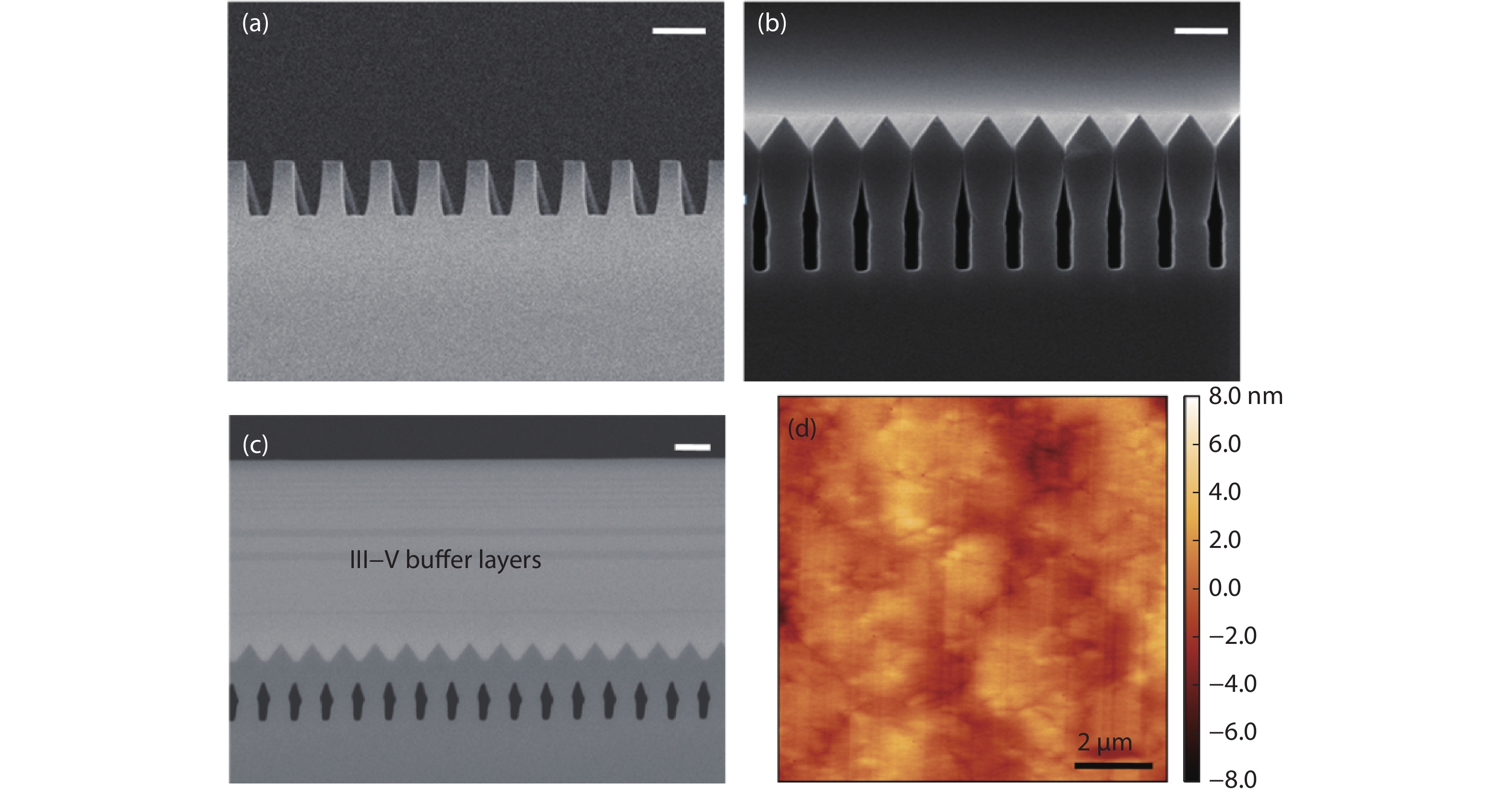
Silicon-based photonic integration has attracted the interest of semiconductor scientists because it has high luminous efficiency and electron mobility. Breakthroughs have been made in silicon-based integrated lasers over the past few decades. Here we review three main methods of integration of III–V materials on Si, namely direct growth, bonding, and selective-area hetero-epitaxy. The III–V materials we introduced mainly include materials such as GaAs and InP. The lasers are mainly lasers of related communication bands. We also introduced the advantages and challenges of the three methods.


J. Semicond.
2019, 40(10): 101306 doi: 10.1088/1674-4926/40/10/101306

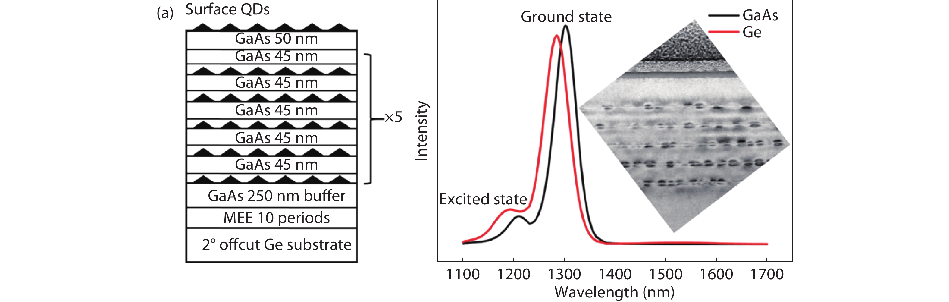
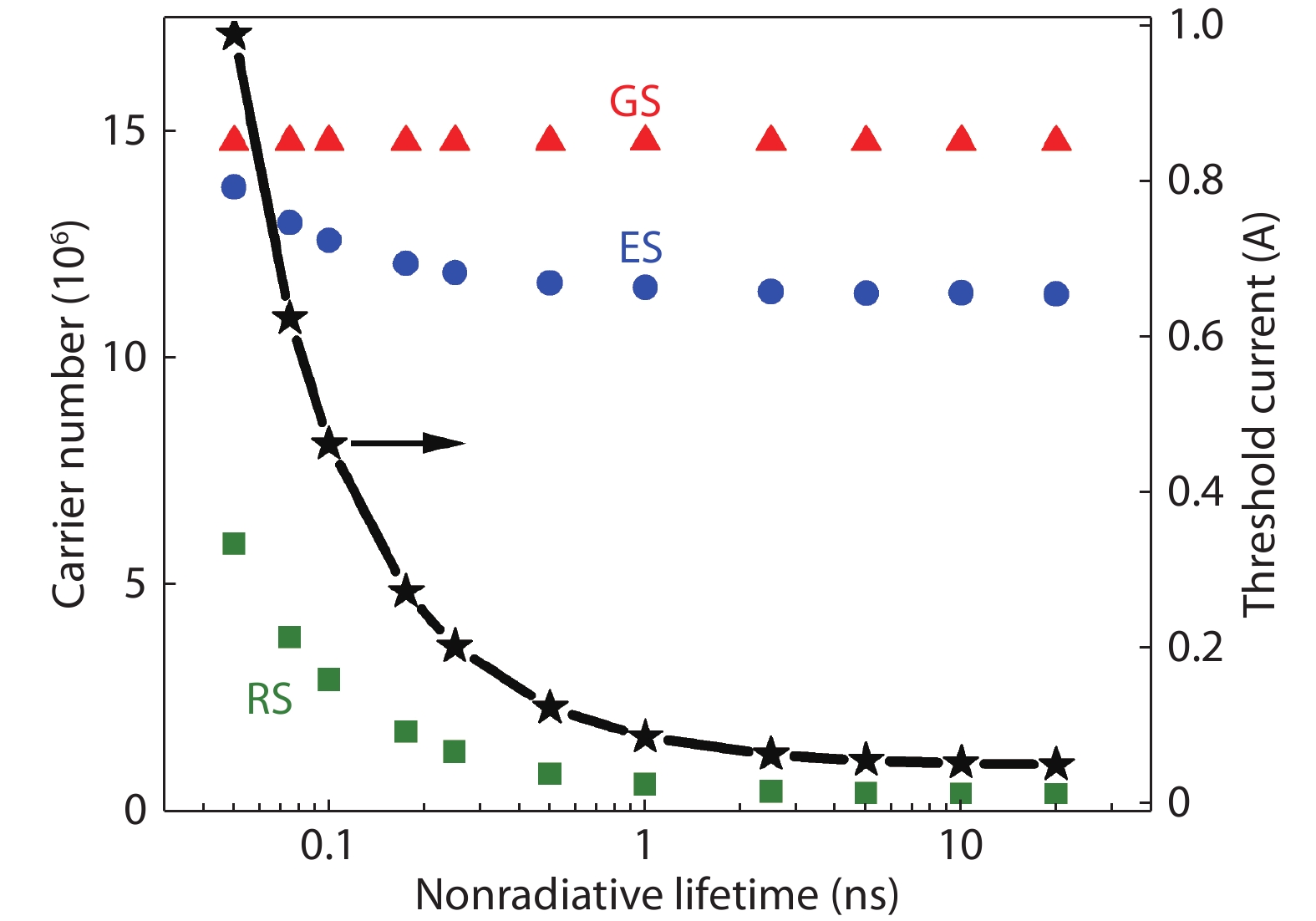
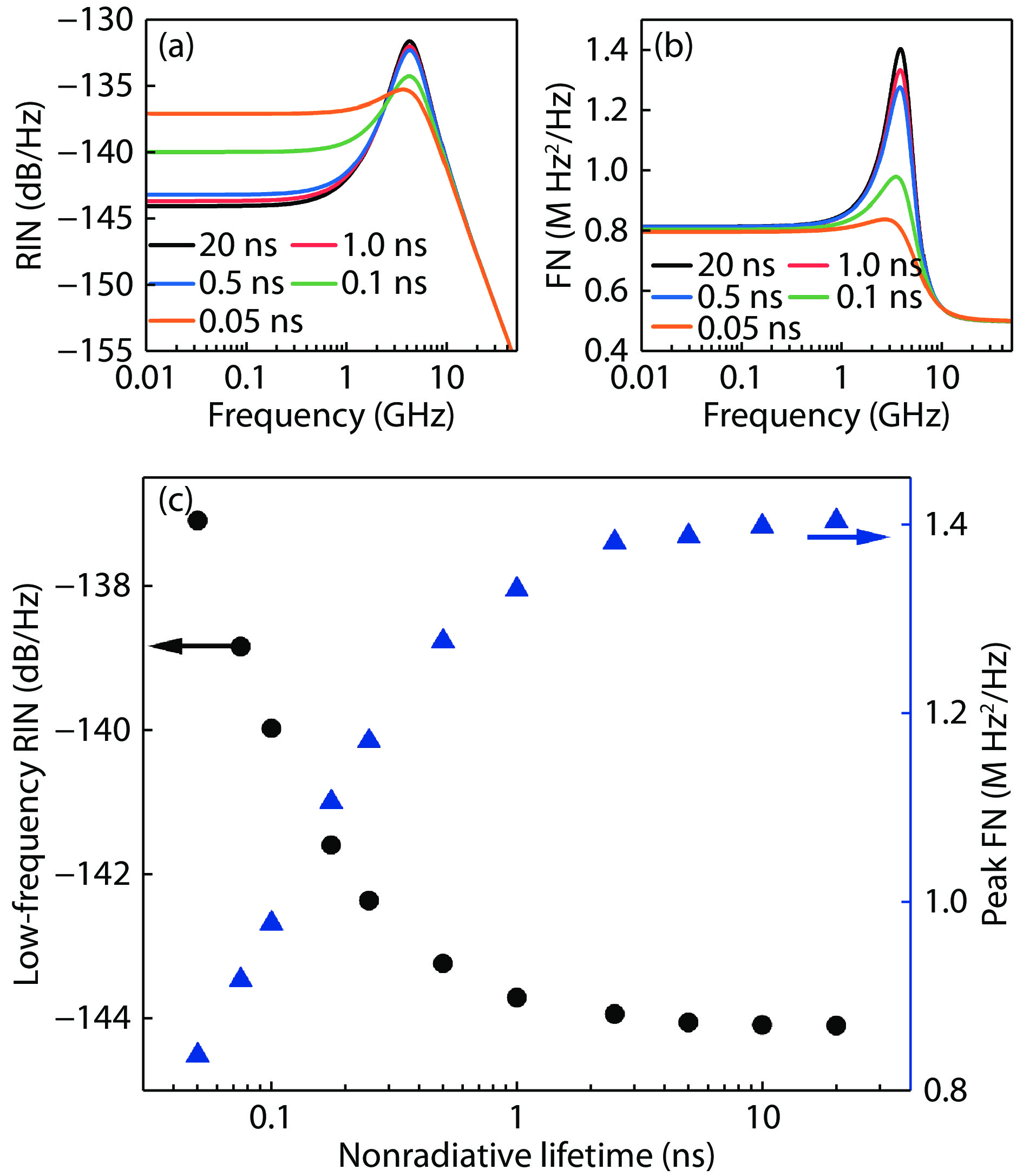
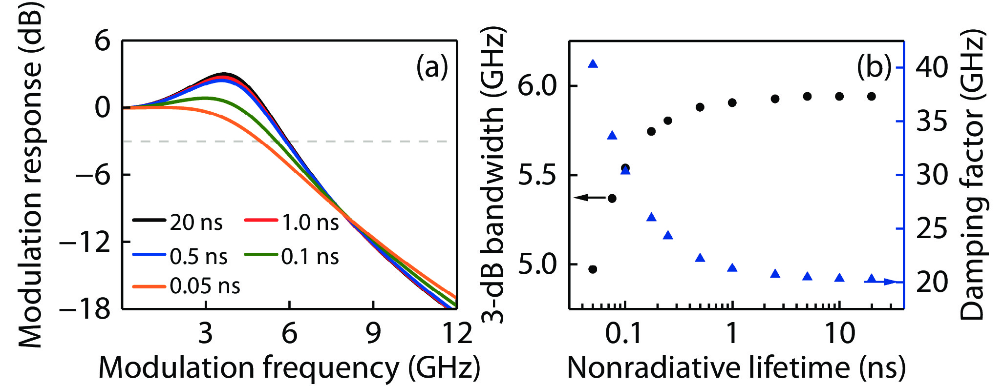
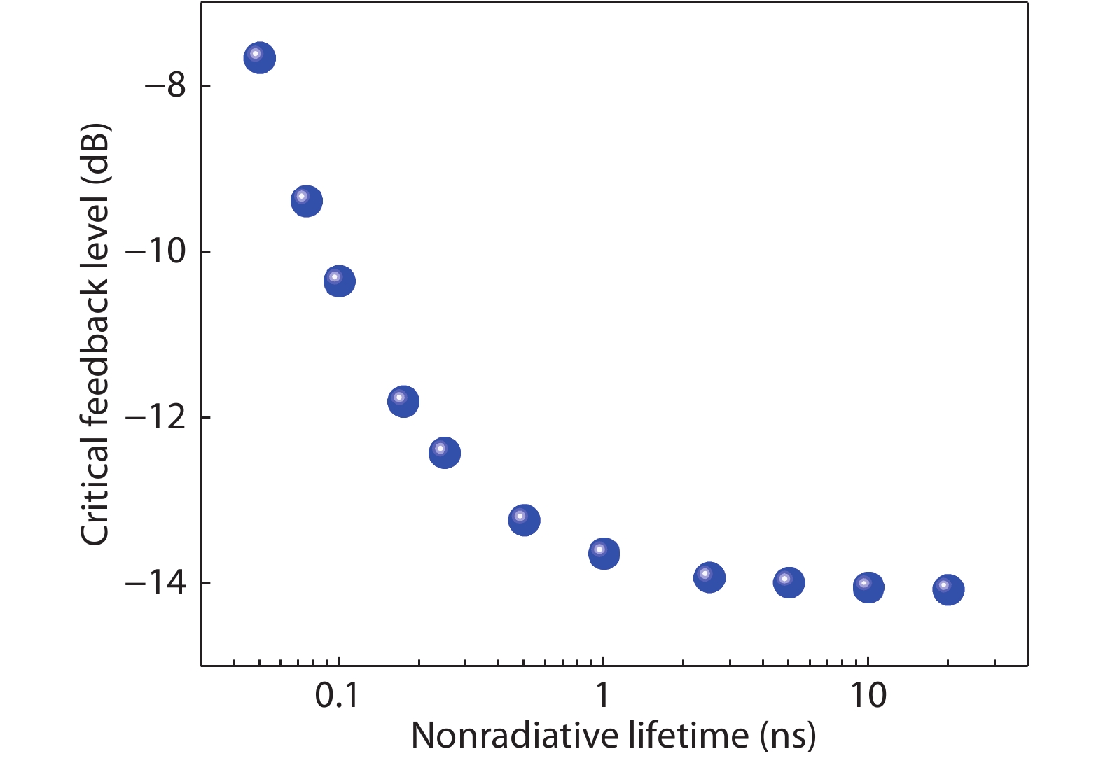
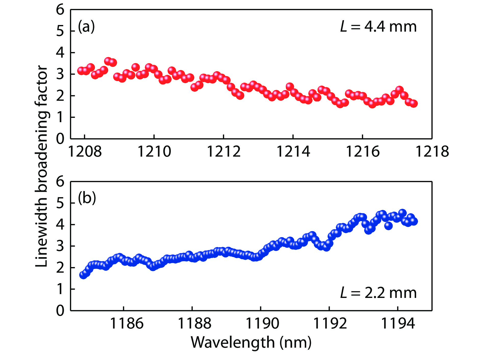
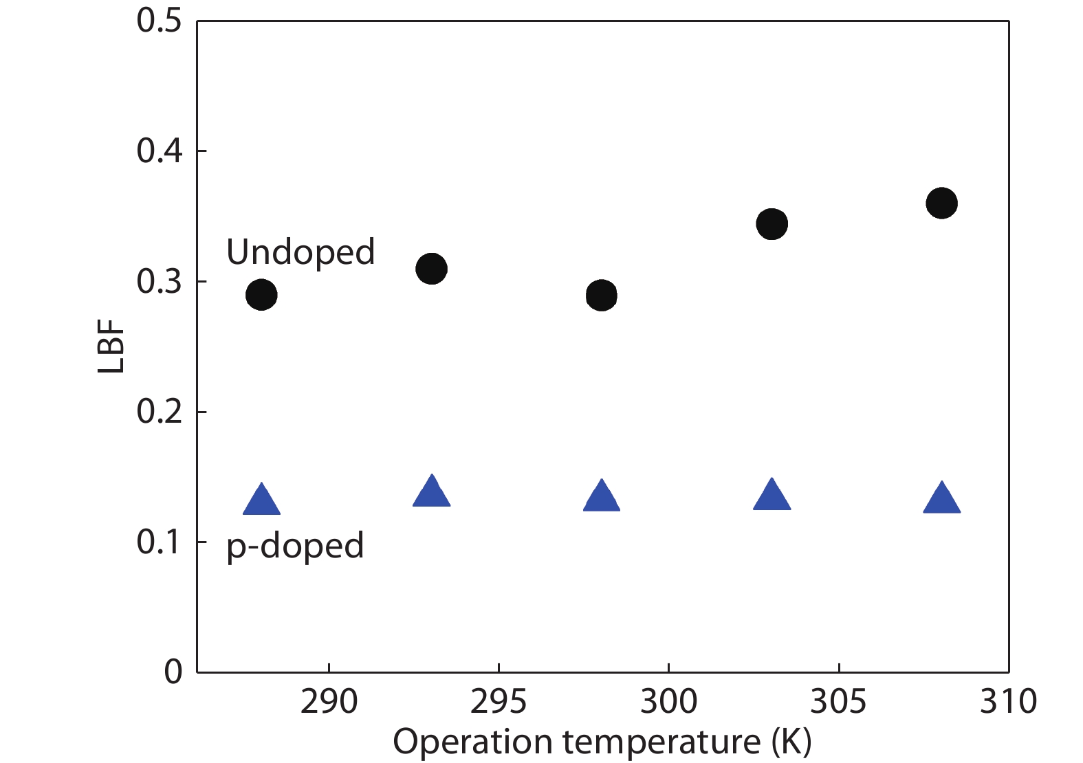
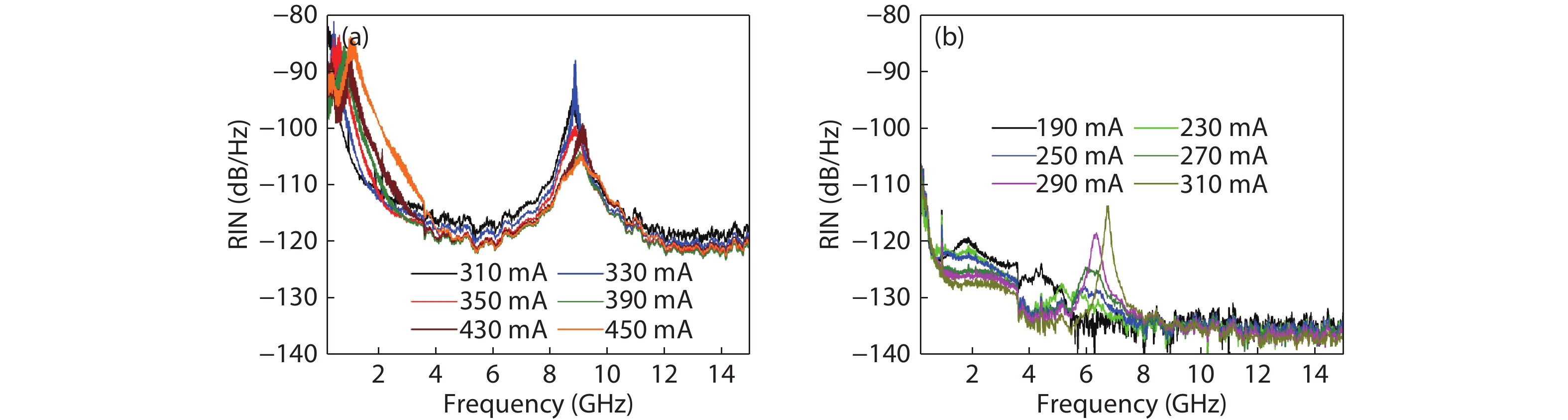
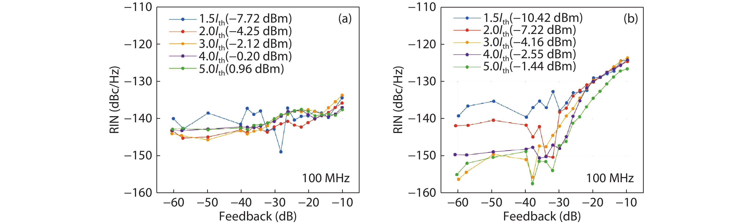
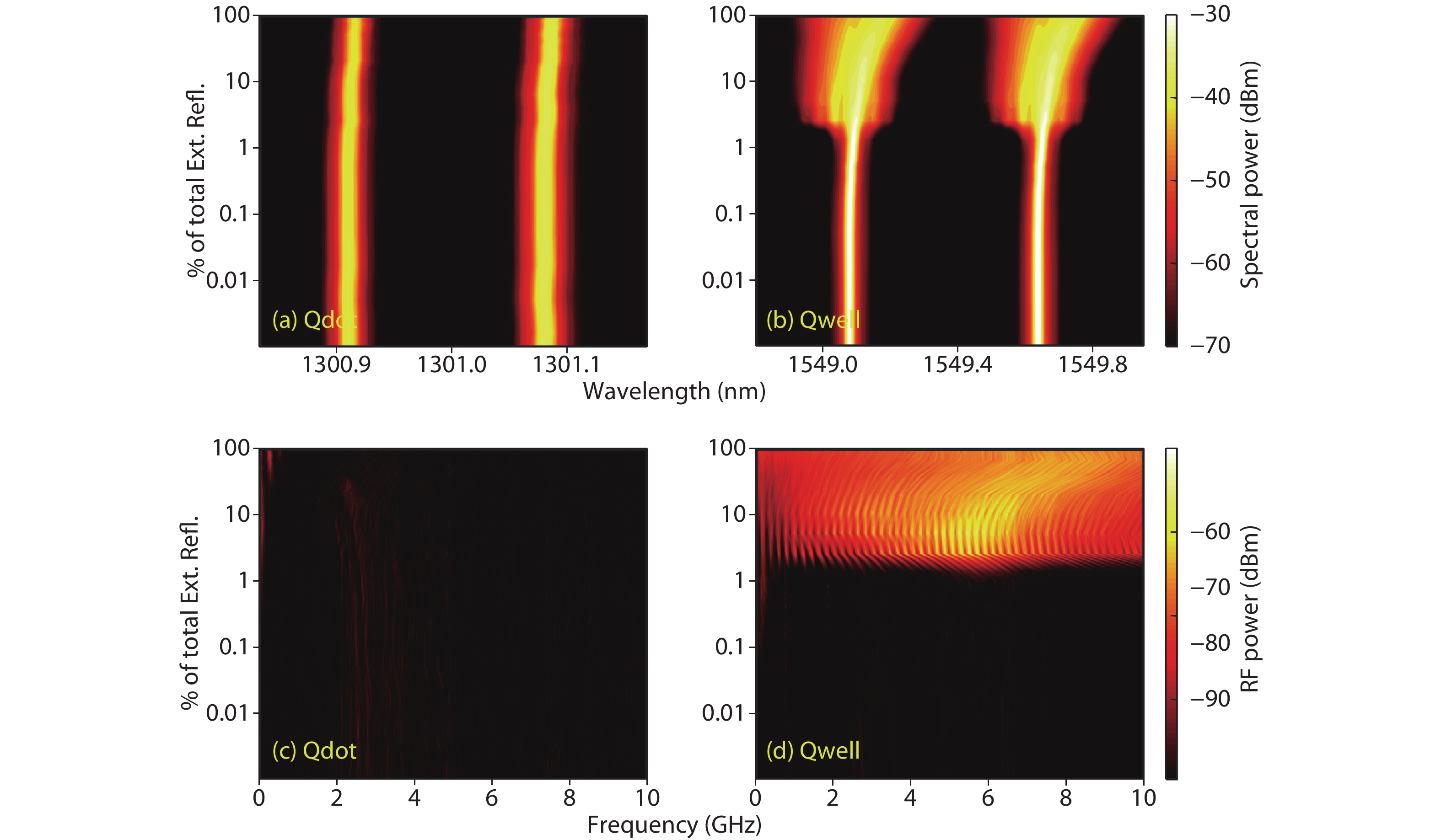
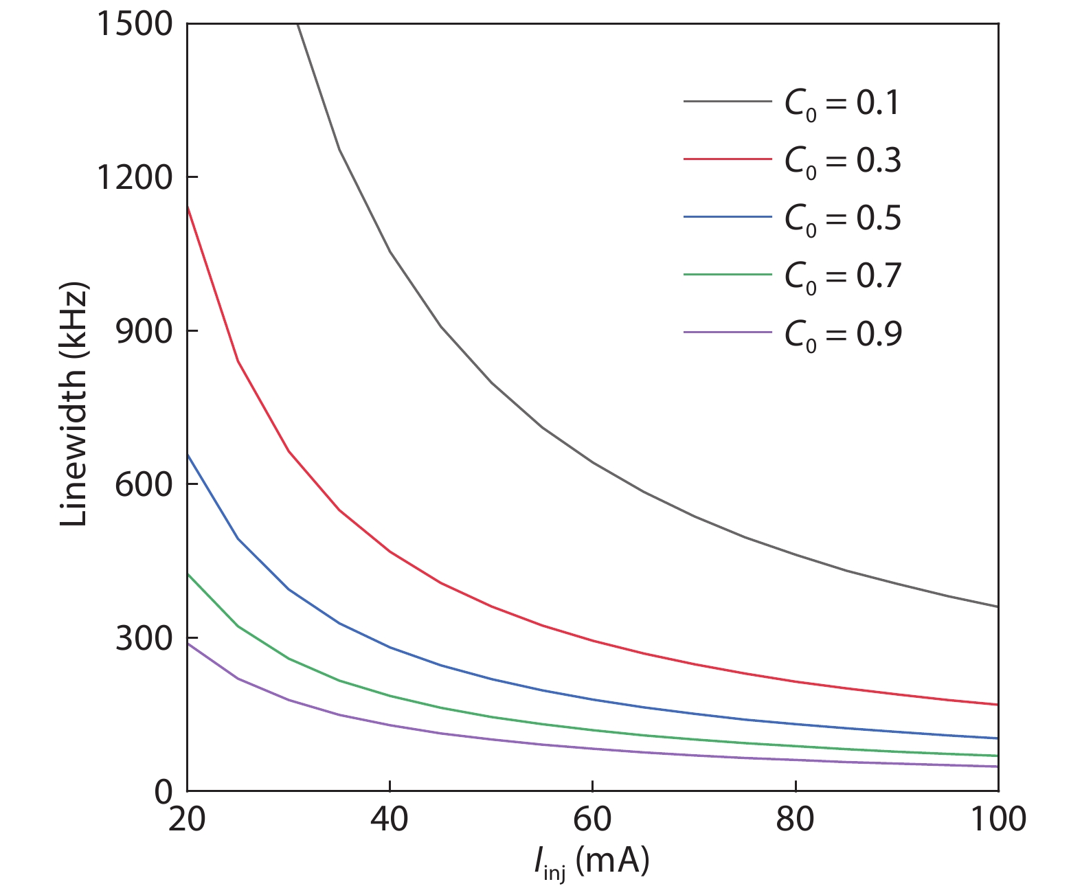
Growing semiconductor laser sources on silicon is a crucial but challenging technology for developing photonic integrated circuits (PICs). InAs/GaAs quantum dot (Qdot) lasers have successfully circumvented the mismatch problem between III–V materials and Ge or Si, and have demonstrated efficient laser emission. In this paper, we review dynamical characteristics of Qdot lasers epitaxially grown on Ge or Si, in comparison with those of Qdot lasers on native GaAs substrate. We discuss properties of linewidth broadening factor, laser noise and its sensitivity to optical feedback, intensity modulation, as well as mode locking operation. The investigation of these dynamical characteristics is beneficial for guiding the design of PICs in optical communications and optical computations.


J. Semicond.
2019, 40(10): 101801 doi: 10.1088/1674-4926/40/10/101801
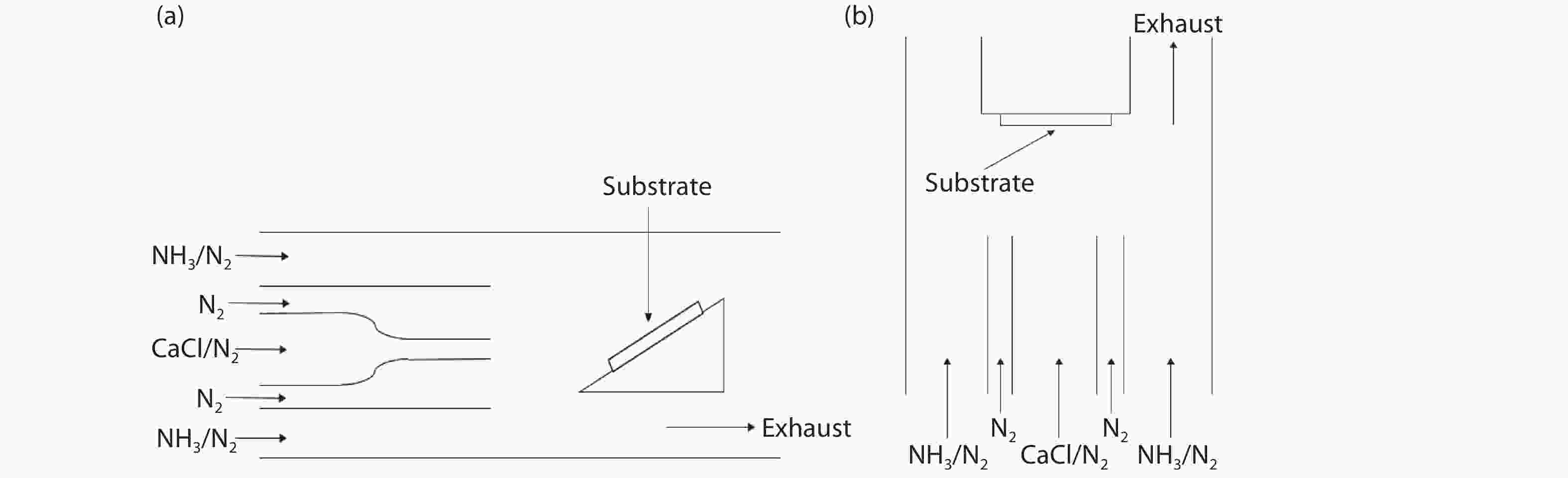
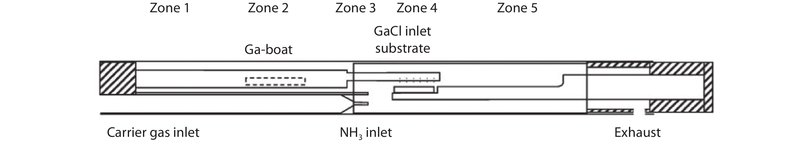
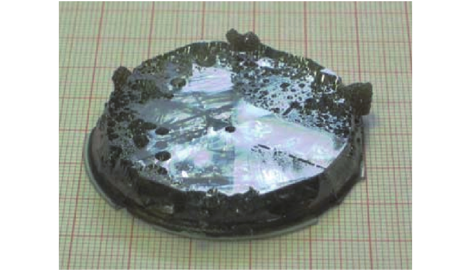
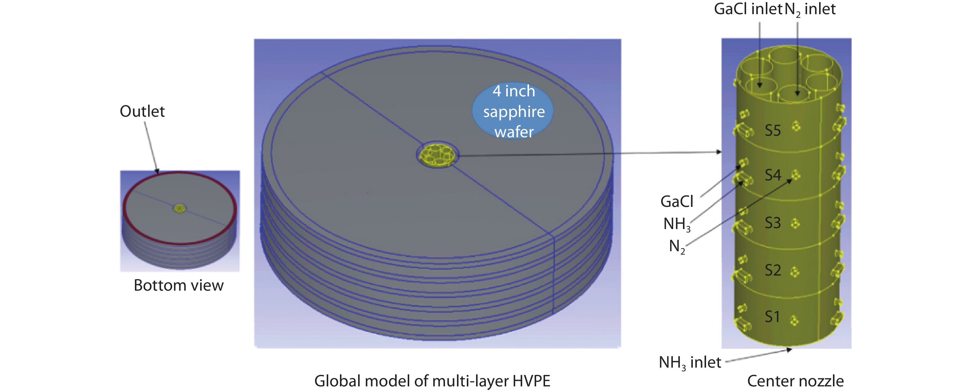
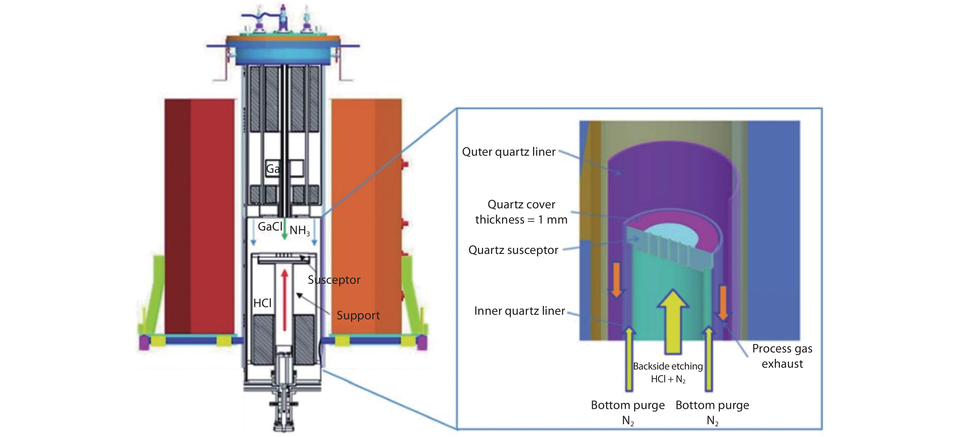
Due to the remarkable growth rate compared to another growth methods for gallium nitride (GaN) growth, hydride vapor phase epitaxy (HVPE) is now the only method for mass product GaN substrates. In this review, commercial HVPE systems and the GaN crystals grown by them are demonstrated. This article also illustrates some innovative attempts to develop homebuilt HVPE systems. Finally, the prospects for the further development of HVPE for GaN crystal growth in the future are also discussed.


J. Semicond.
2019, 40(10): 102301 doi: 10.1088/1674-4926/40/10/102301
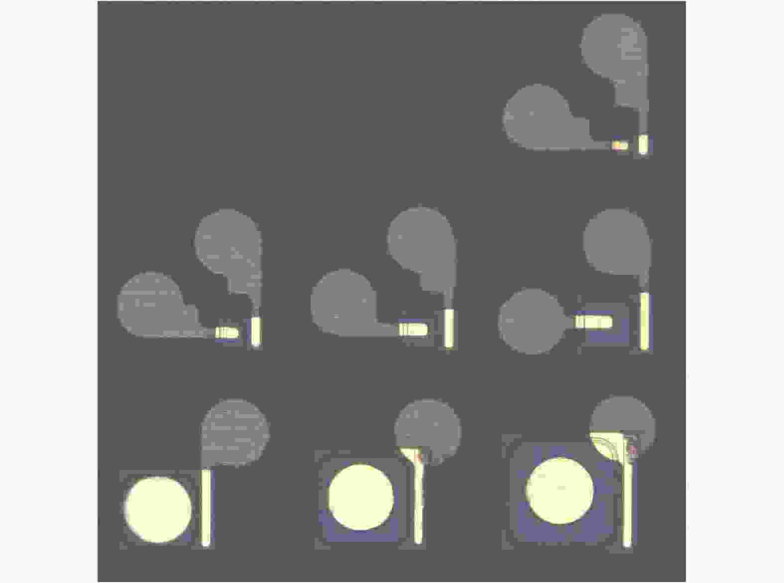
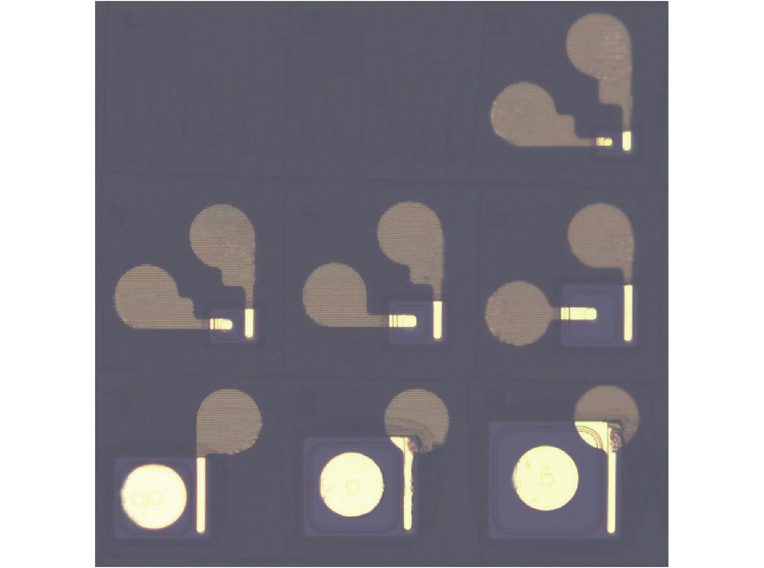
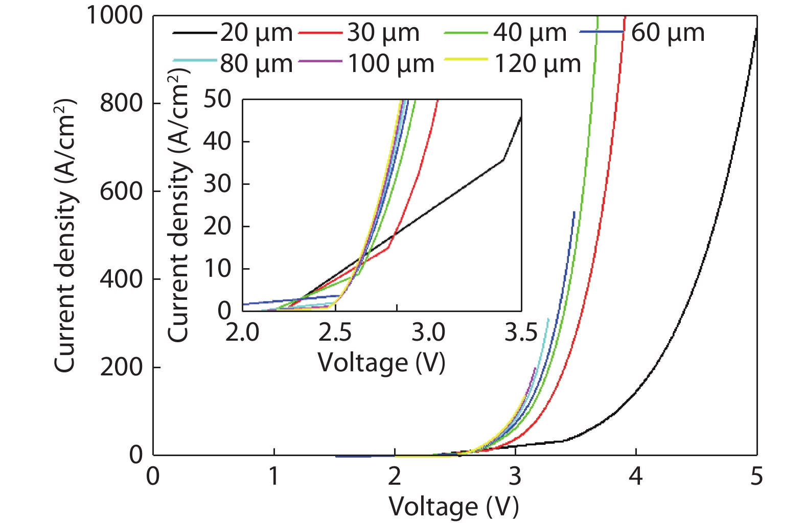
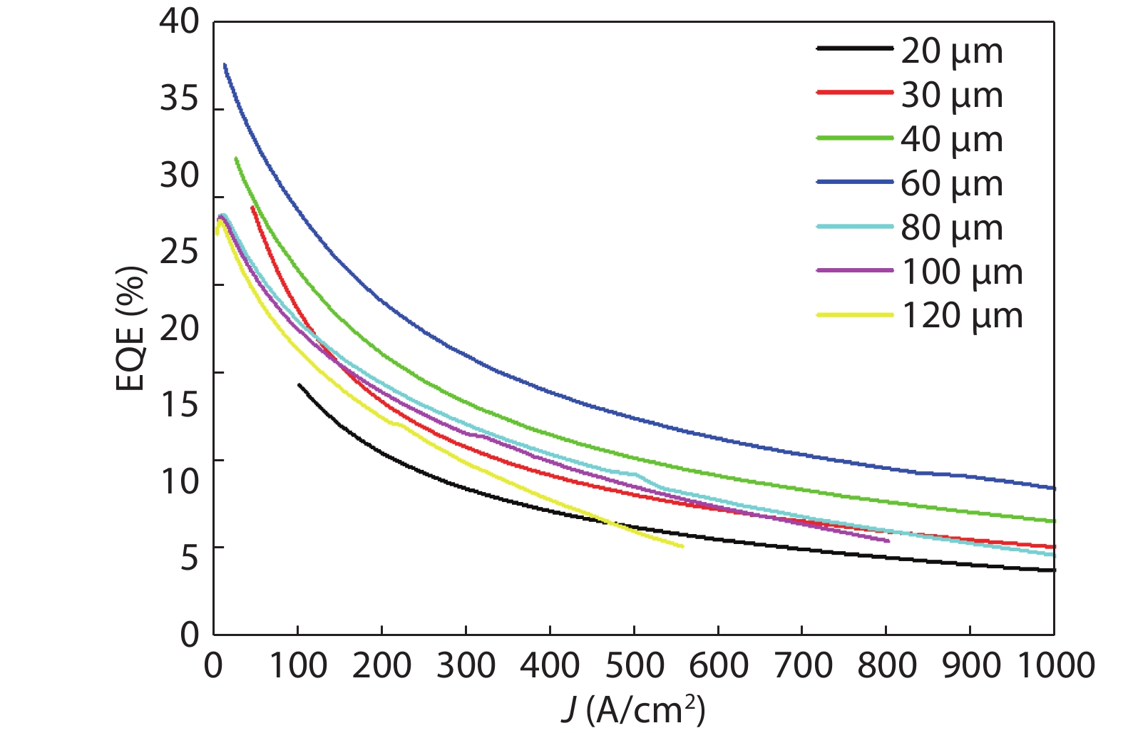
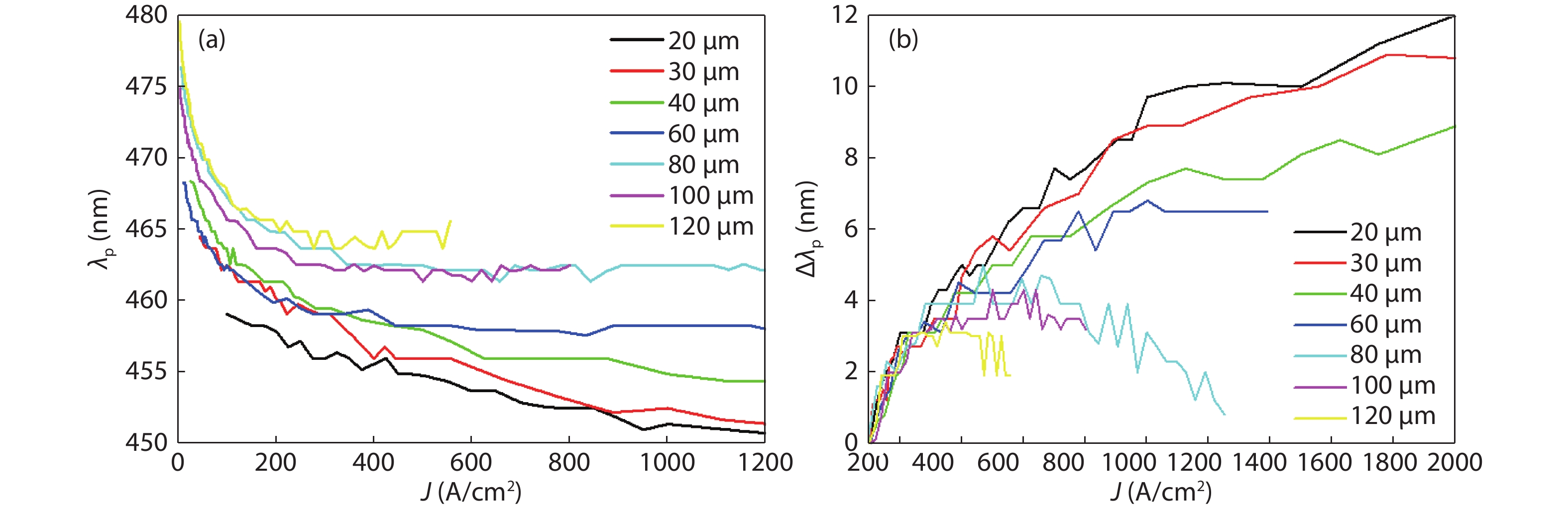
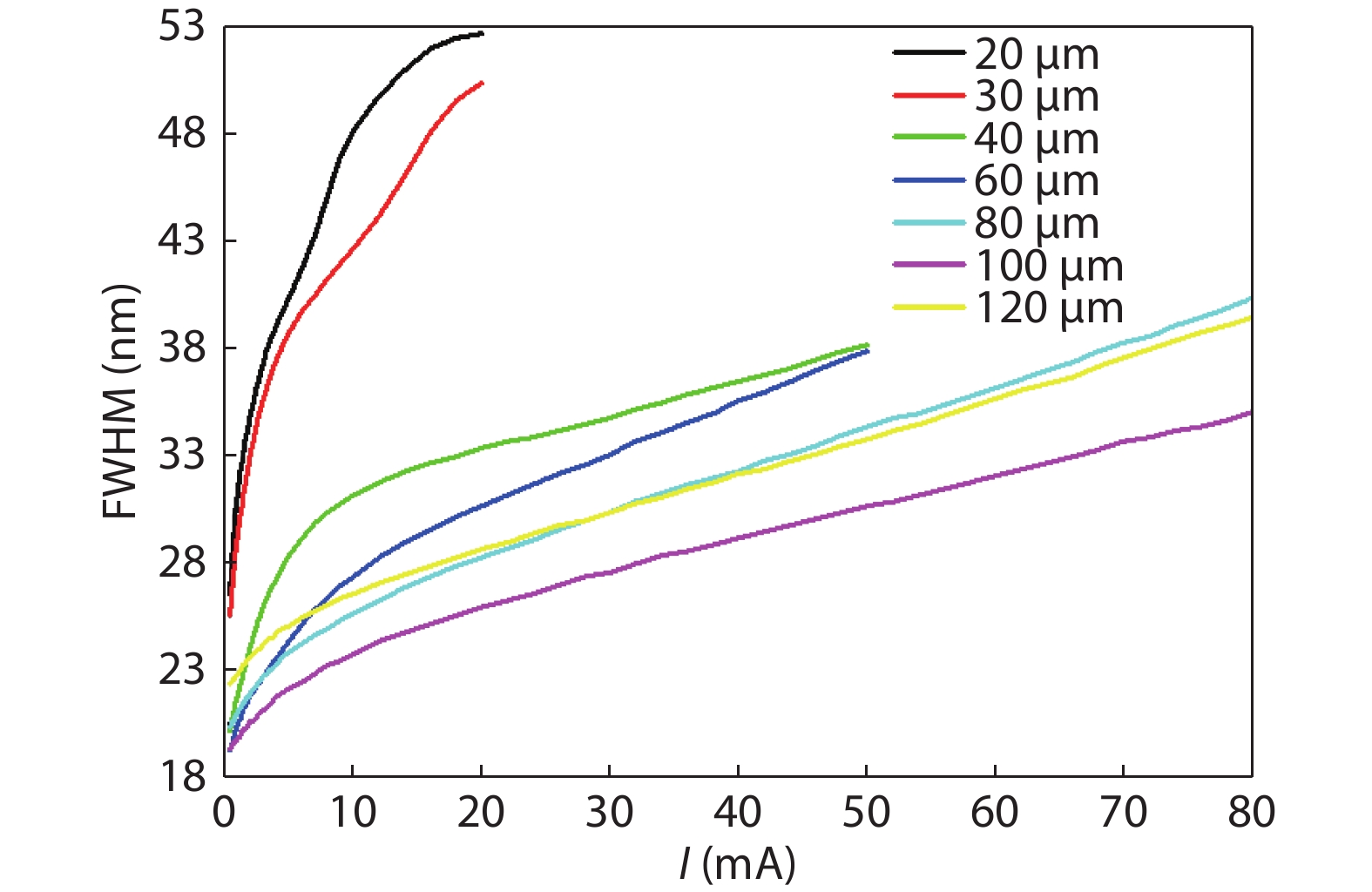
In this paper, size effects on optical performance of blue light-emitting diodes (LEDs) are investigated. The essential physical mechanism is studied by fabricating LEDs with various sizes of the active area and testing optical characteristics. It is found that micro-LEDs have better light extracting efficiency and thermal dissipation compared with broad-area LEDs, which is likely due to the small ratio of perimeter and active area. Furthermore, micro-LEDs are more beneficial for displays due to the stable wavelength under the low pulse width modulation (PWM) current density.

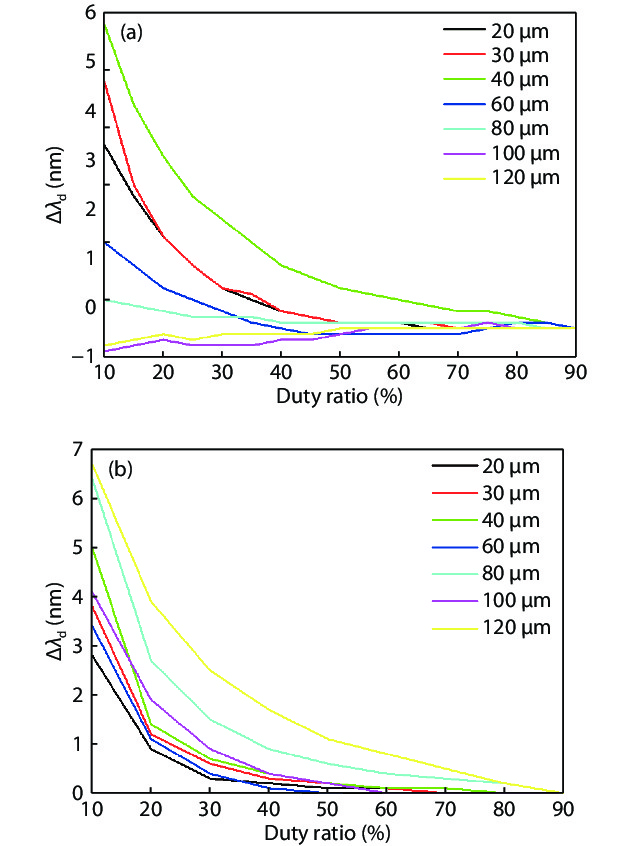
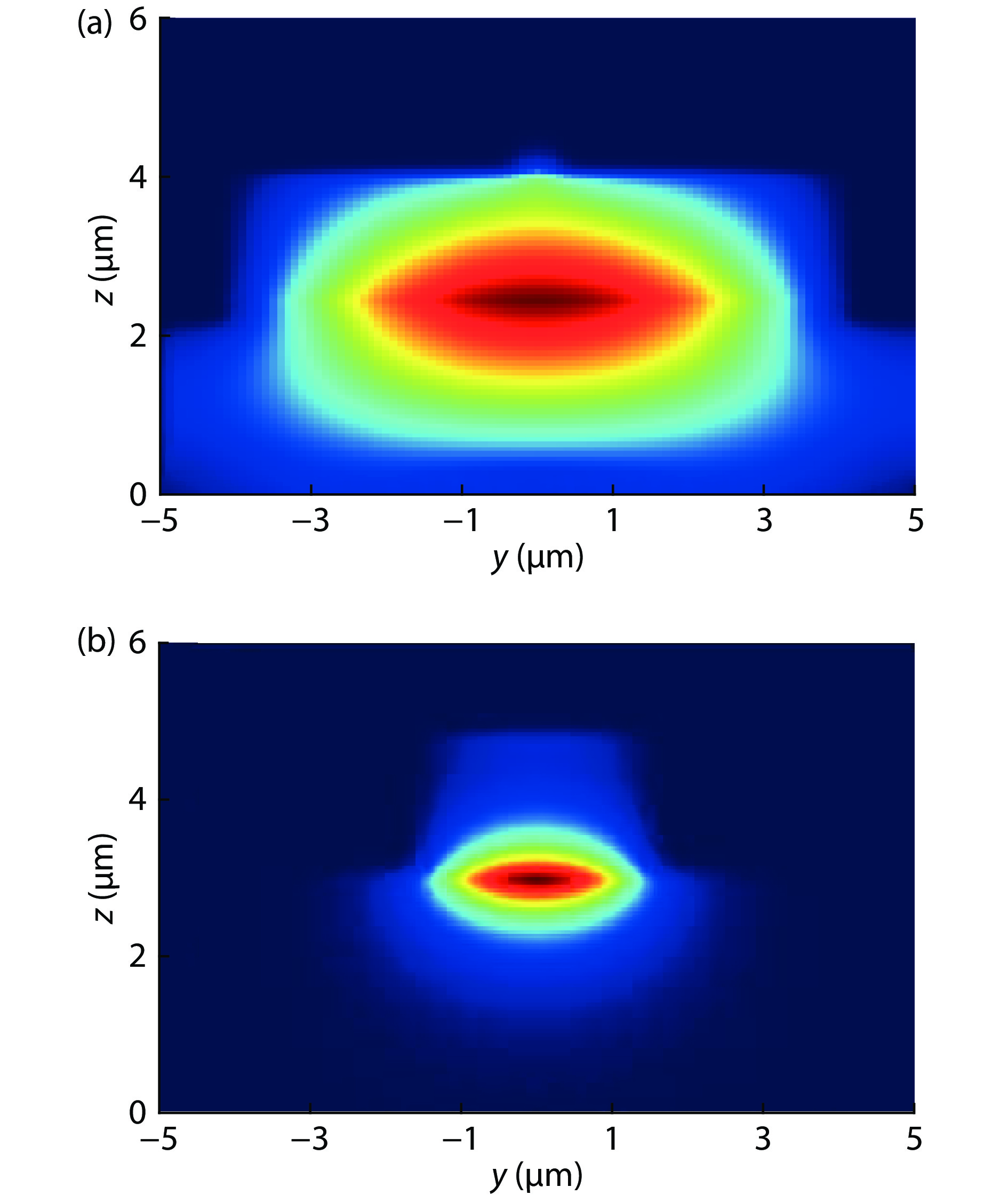
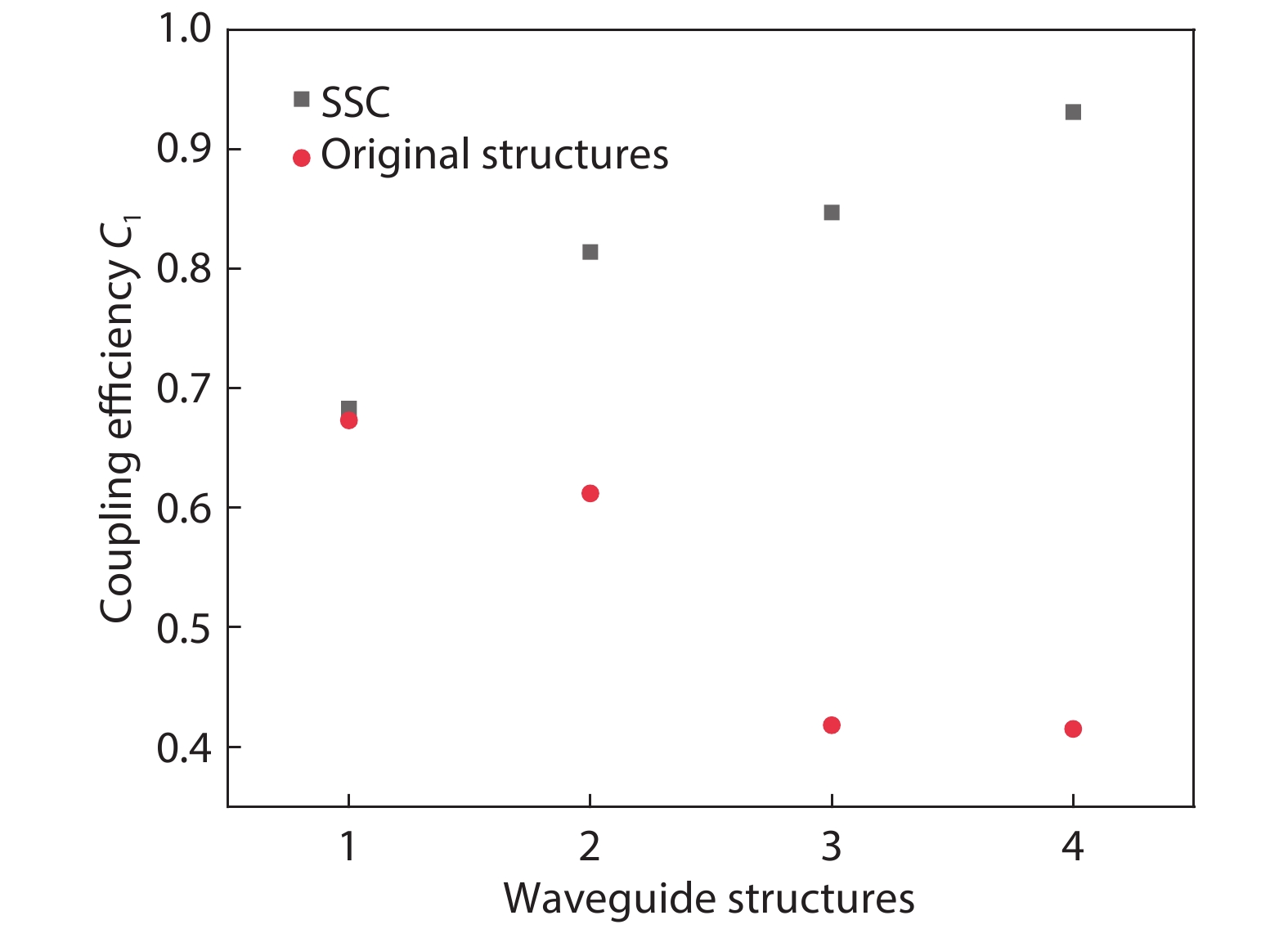
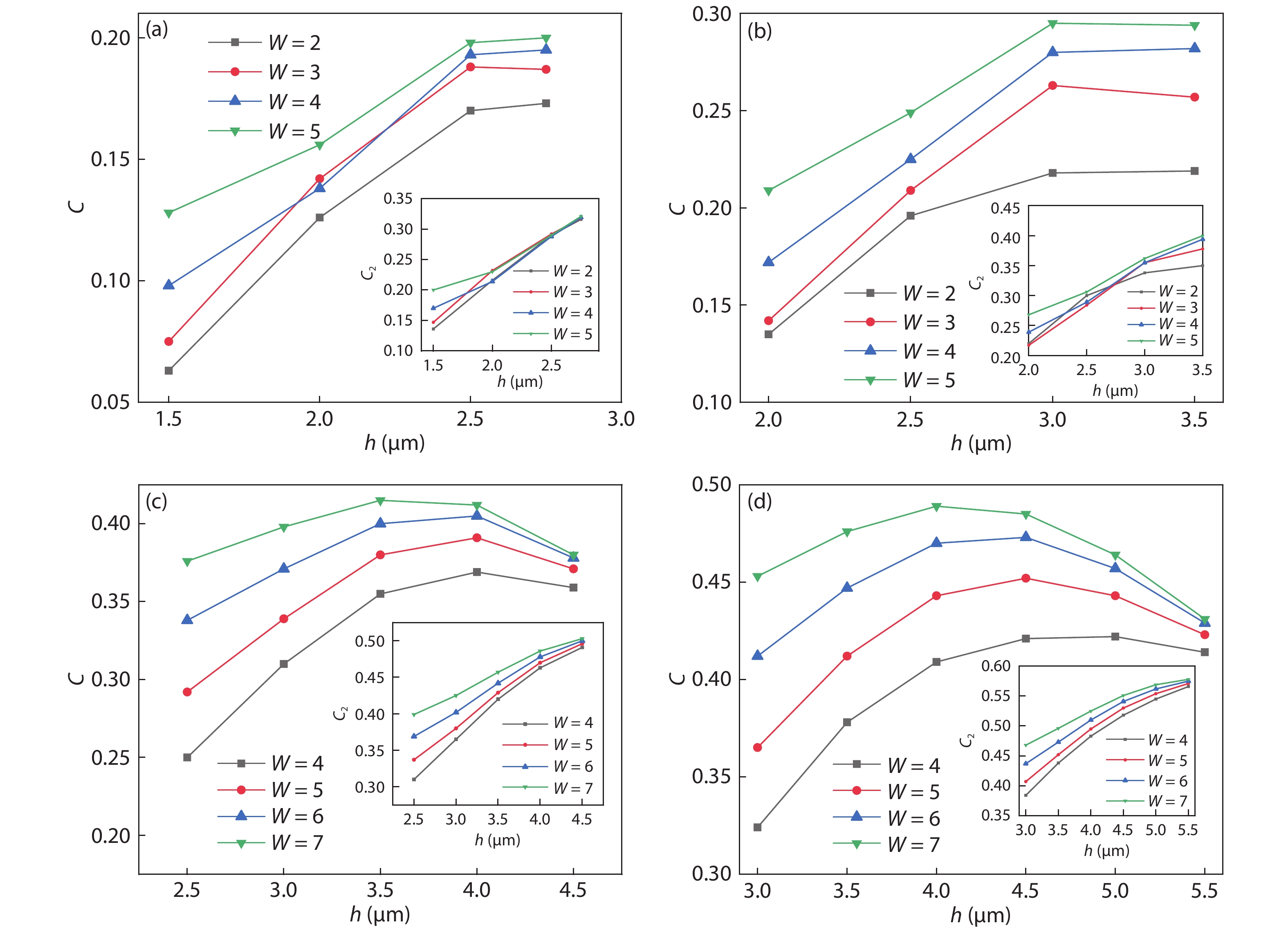
Simulation of structural design with high coupling efficiency in external cavity semiconductor laser
J. Semicond.
2019, 40(10): 102302 doi: 10.1088/1674-4926/40/10/102302

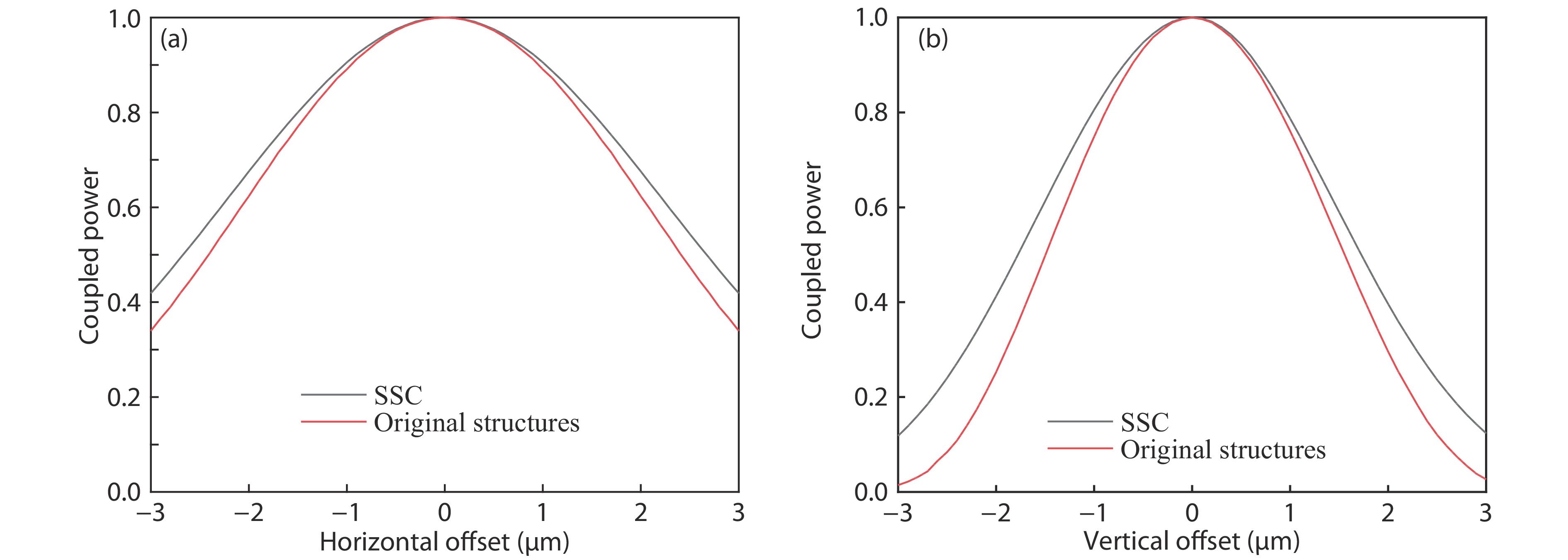
For external cavity semiconductor lasers (ECSLs), high coupling efficiency is critical to reducing the linewidth. In this paper, the coupling efficiency between the laser diode and the waveguide grating has been improved, with proposals for its improvement presented, including adding spot-size conversion (SSC) and using a silicon-on-insulator (SOI) waveguide. The results indicate an increase of coupling efficiency from 41.5% to 93.1%, which exhibits an improvement of approximately 51.6% over conventional schemes. The relationship between coupling efficiency and SOI waveguide structures is mainly concerned in this article. These findings provide a new way for the future research of the narrow linewidth of ECSL.


J. Semicond.
2019, 40(10): 102801 doi: 10.1088/1674-4926/40/10/102801
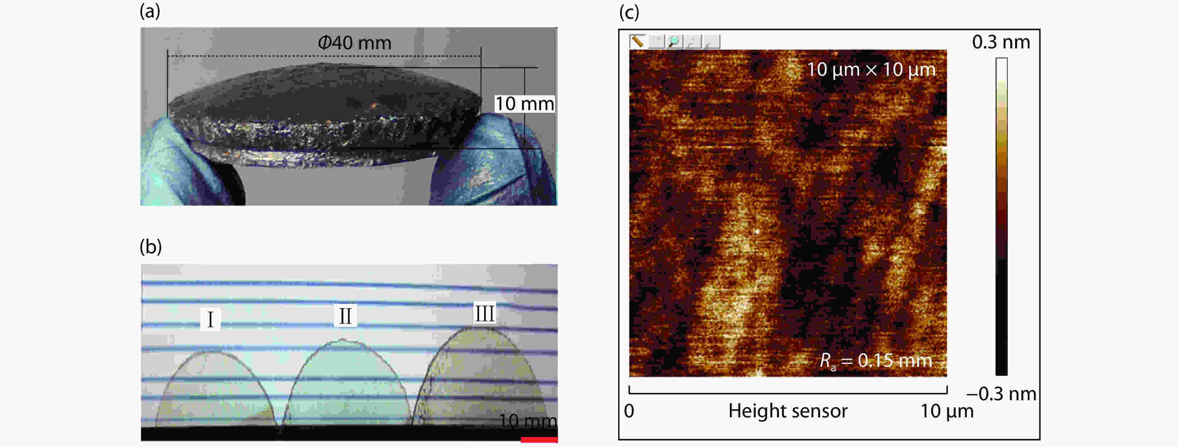
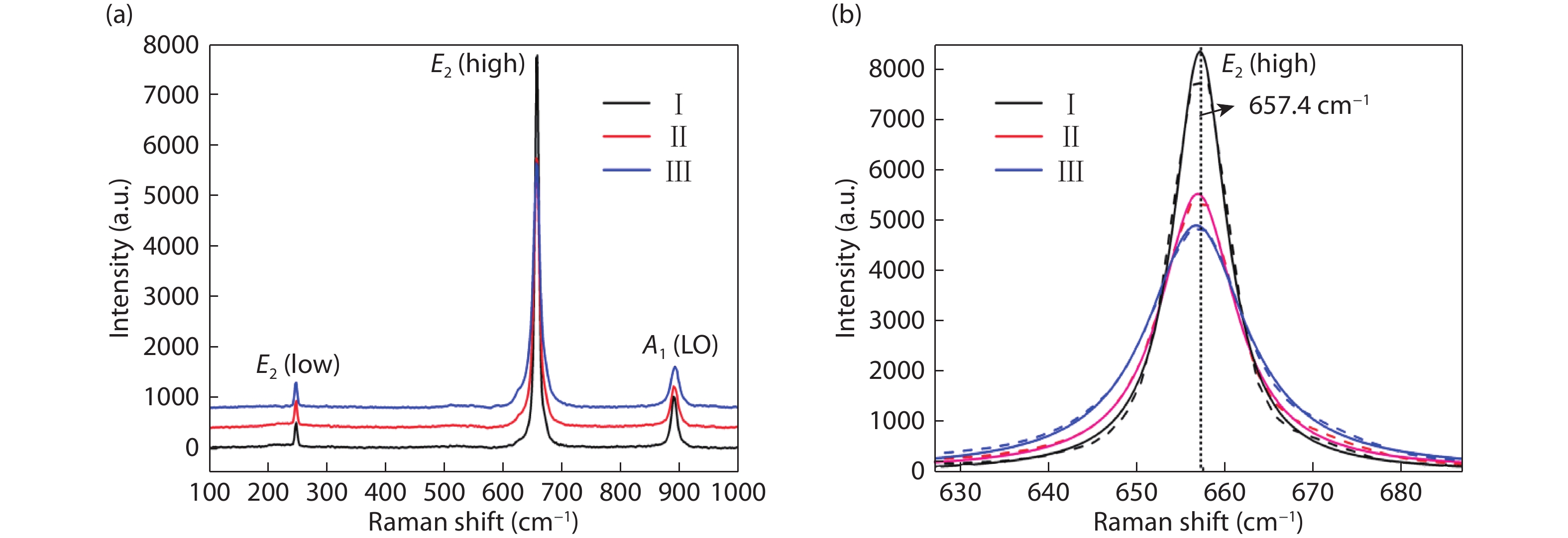
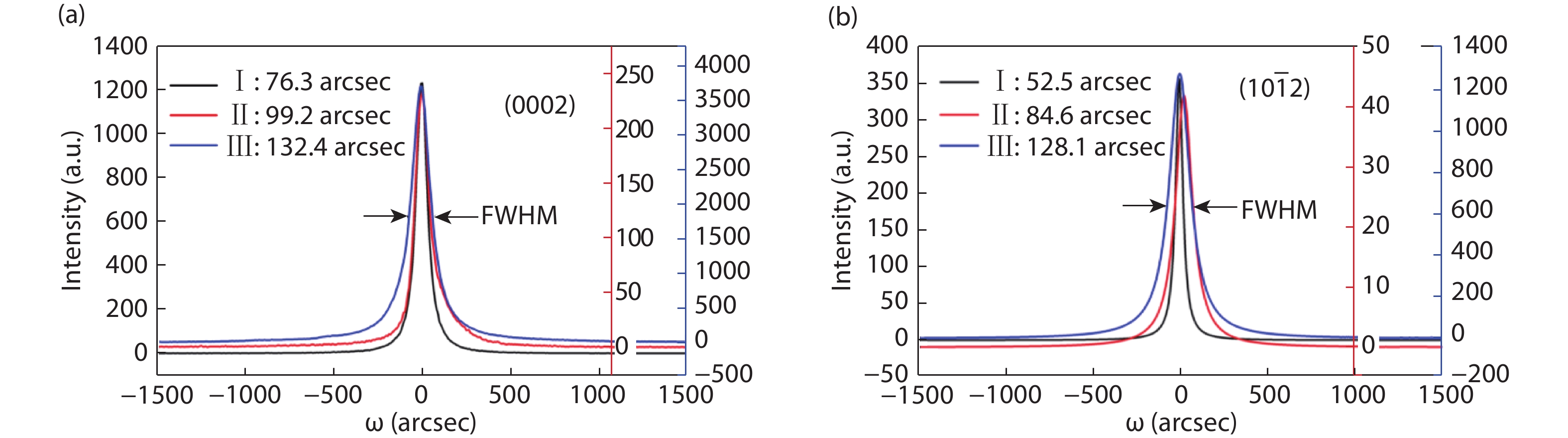
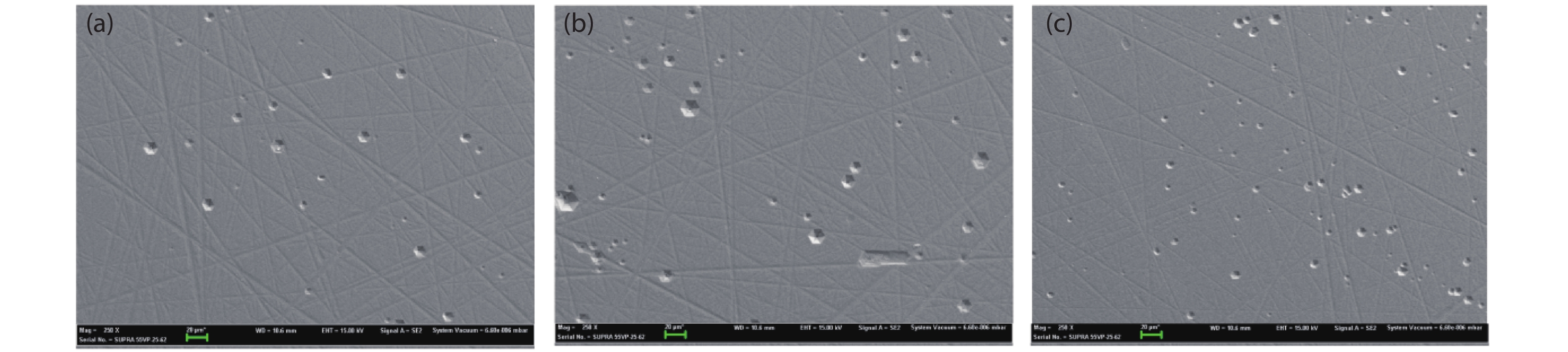
Large size AlN bulk crystal has been grown on SiC heterogeneous seed by physical vapor transport (PVT). The properties of AlN wafer were characterized by high resolution X-ray diffraction (HRXRD), Raman spectroscopy, etched method and atomic force microscope (AFM). Growth mechanism of AlN crystal grown on heterogeneous SiC seeds was proposed. Crystallization quality of AlN samples were improved with the growth process, which is associated with the growth mechanism. AlN single wafer has excellent crystallization quality, which is indicated by HRXRD showing the (0002), (