Issue Browser
Volume 40, Issue 2,
Feb 2019

J. Semicond.
2019, 40(2): 020301 doi: 10.1088/1674-4926/40/2/020301

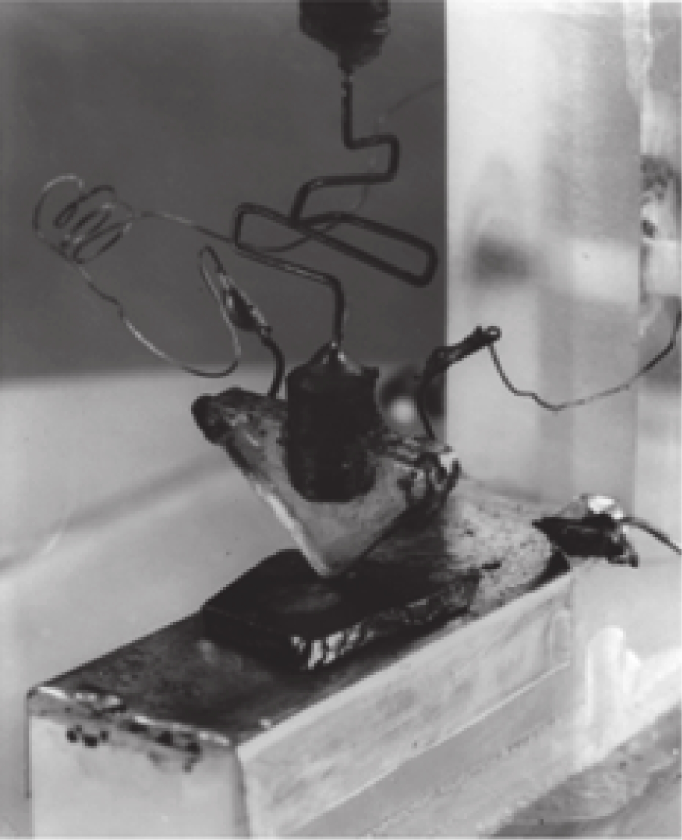
Transistor’s invention revolutionized global society by spawning electronics industry. John Bardeen is among one of the inventors of transistor. He was a genius and one of the most influential semiconductor Physicist of 20th century who won two Nobel prizes in Physics.


J. Semicond.
2019, 40(2): 022101 doi: 10.1088/1674-4926/40/2/022101
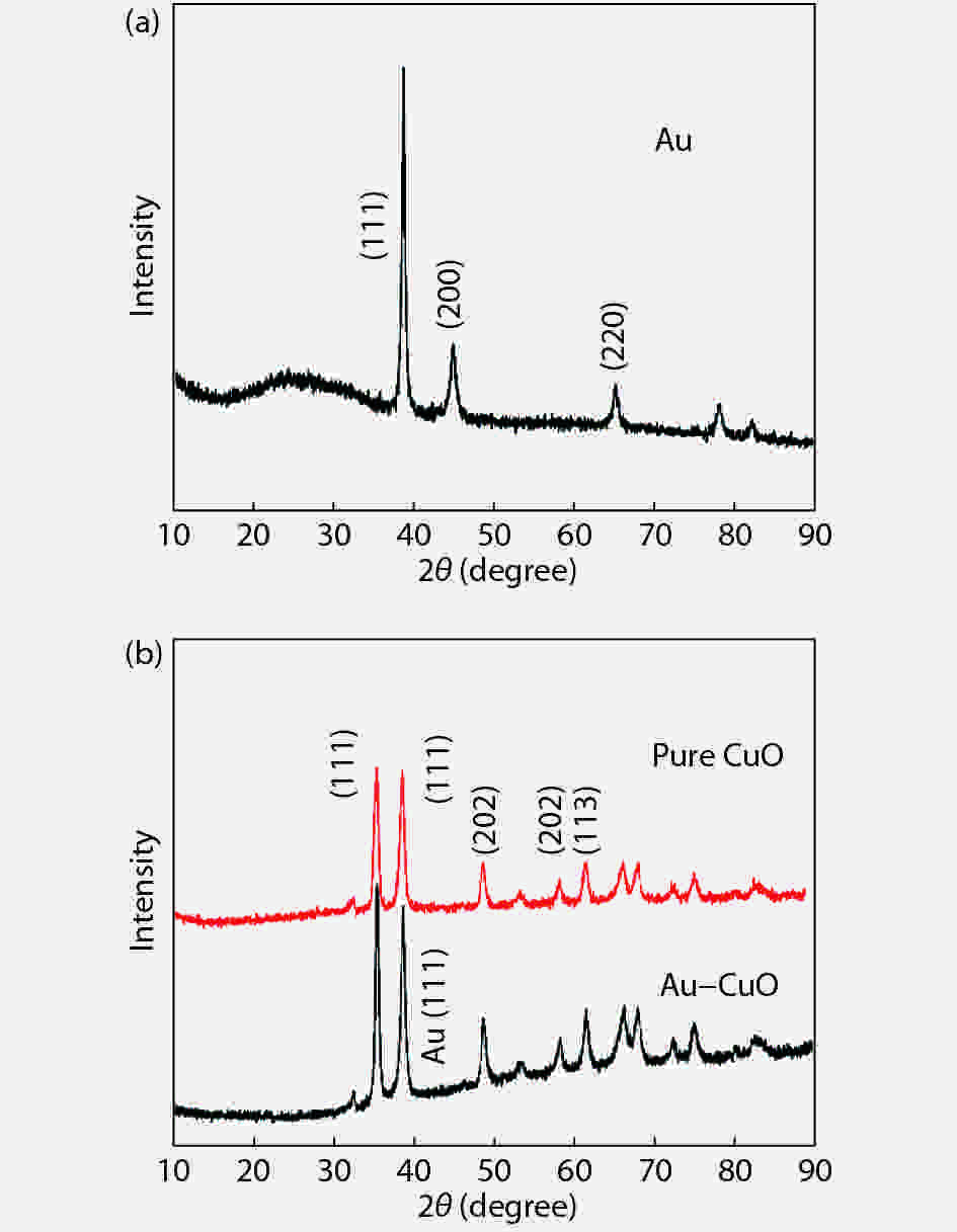
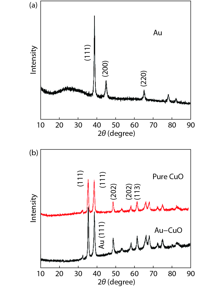
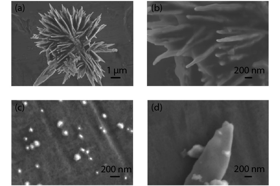
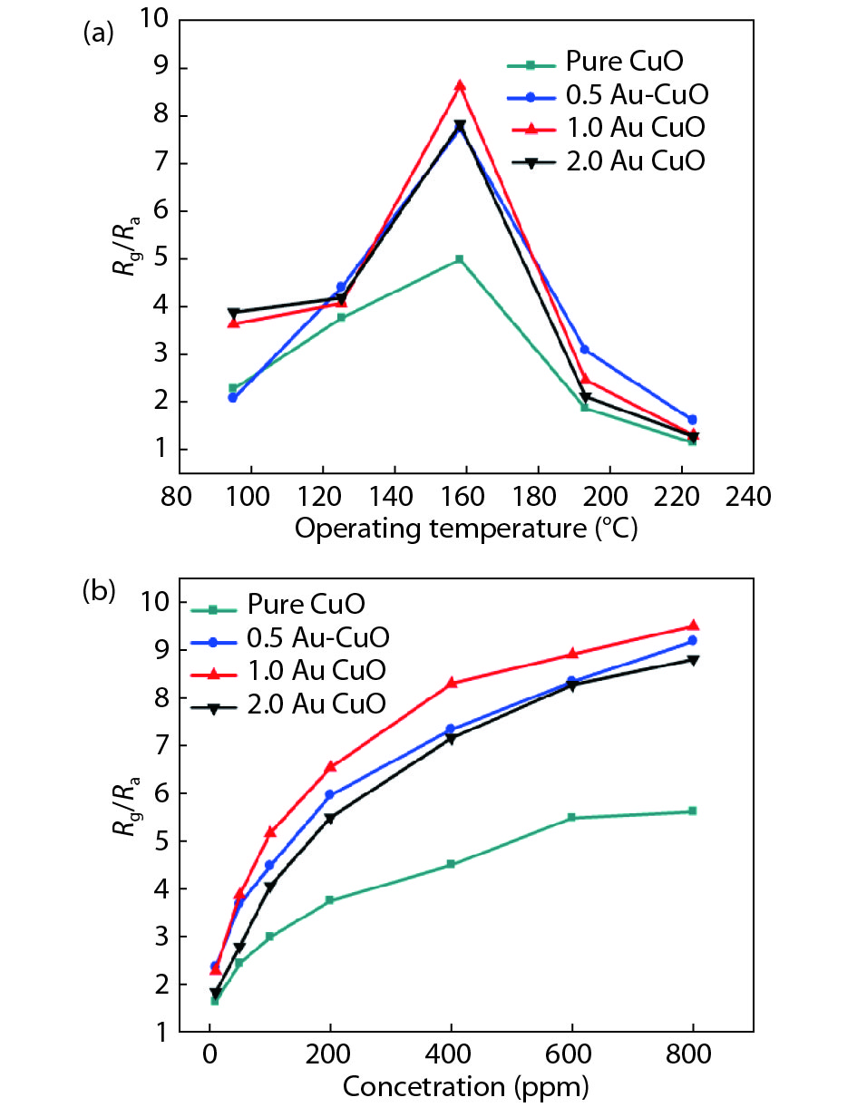
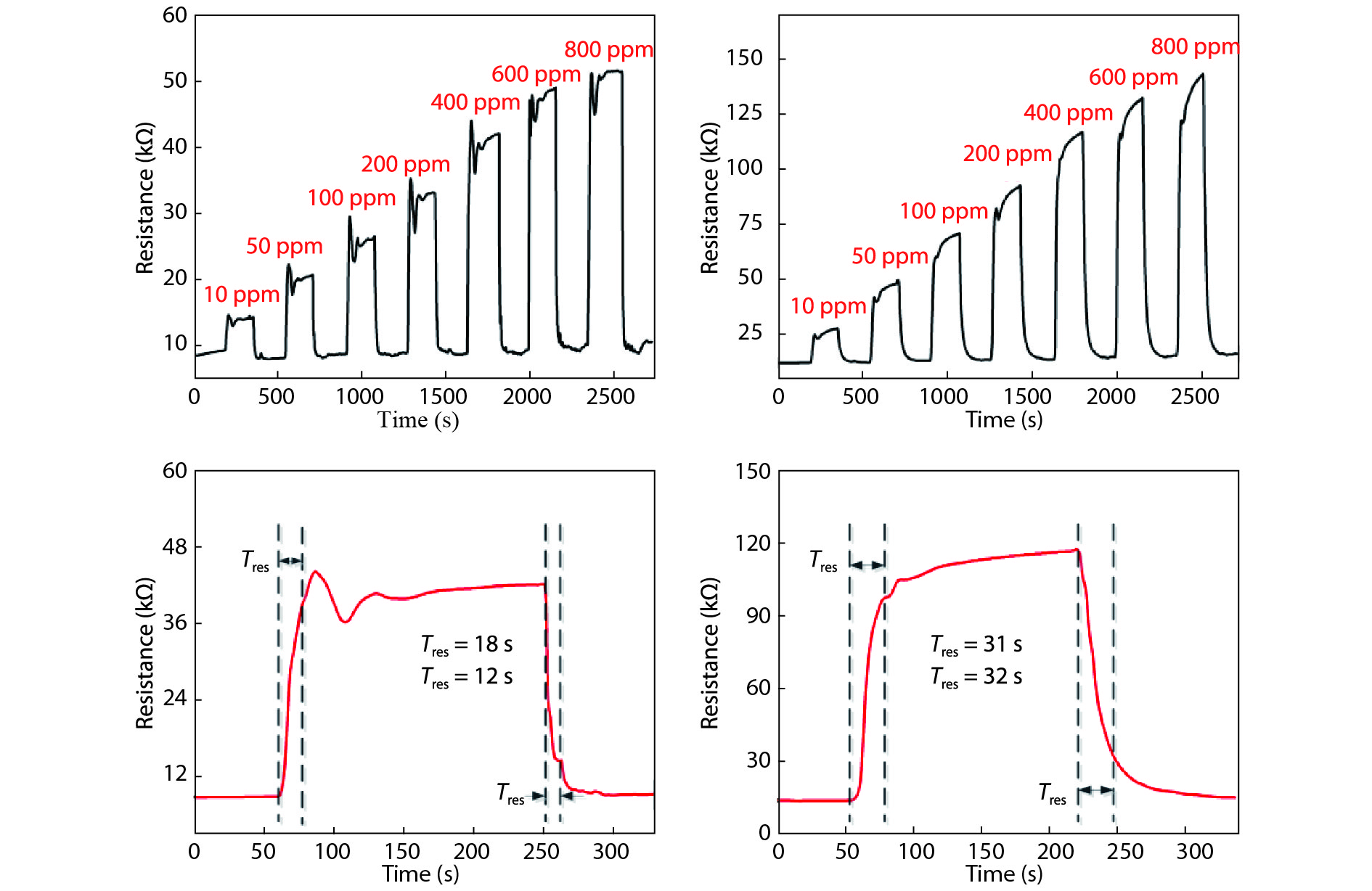
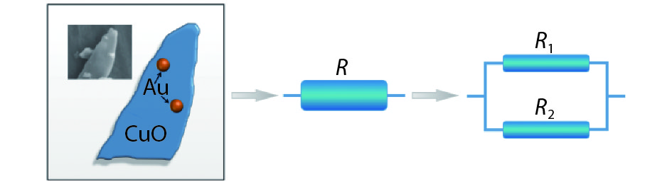
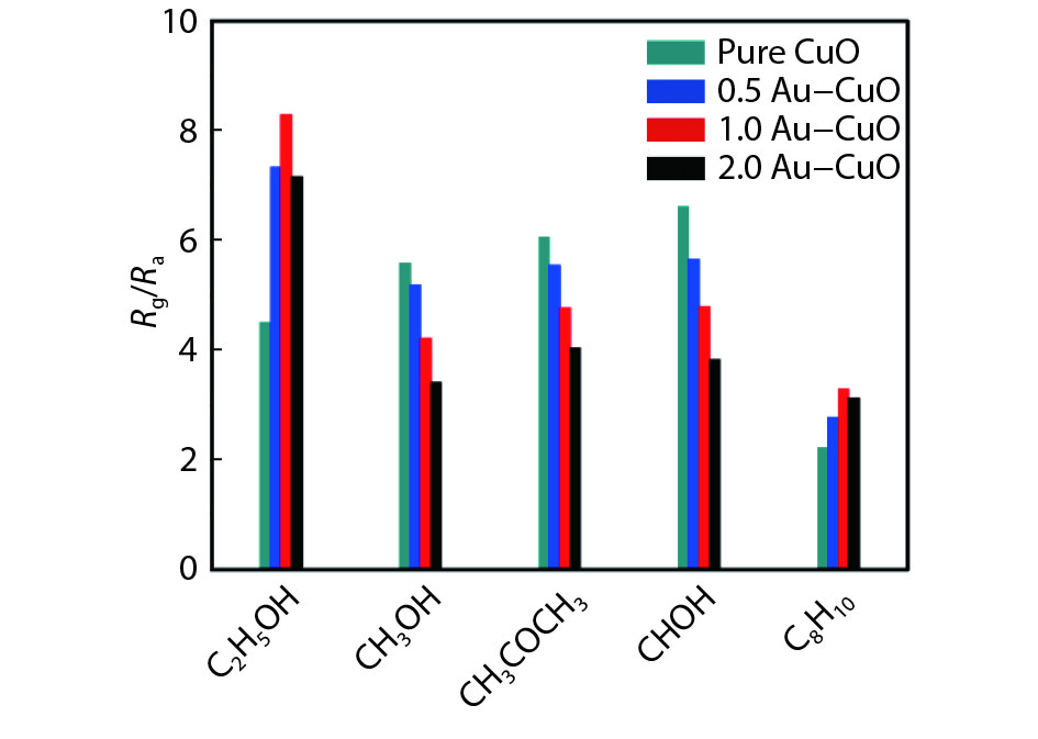
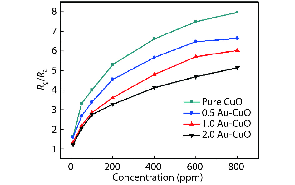
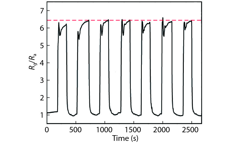
The three-dimensional hierarchical CuO and Au nanoparticles were synthesized by the hydrothermal method, respectively. The hierarchical CuO and the Au nanoparticles samples were characterized by X-ray diffraction and scanning electronic microscope, respectively. The as-synthesized CuO was assembled regularly from the nanosheets with thickness of 100 nm. The size of Au nanoparticles ranged from 50 to 200 nm. The hierarchical CuO gas sensors modified by different concentration of gold were fabricated. All the Au-loaded CuO gas sensors enhanced the response to ethanol and xylene while reducing the response to methanol, acetone, and formaldehyde. The results indicate that the Au nanoparticles prepared with PVP as surfactant can improve the selectivity of CuO gas sensors to ethanol gas for other common organic volatile gases. The improvement of gas sensing is mainly attributed to the different catalytic efficiency of the Au nanoparticles for different reactions. Meanwhile, the related mechanisms are discussed.
J. Semicond.
2019, 40(2): 022401 doi: 10.1088/1674-4926/40/2/022401

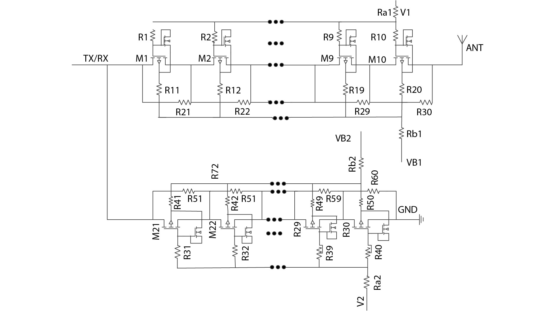
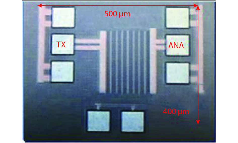
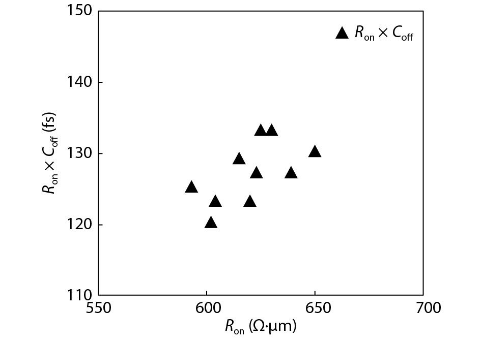
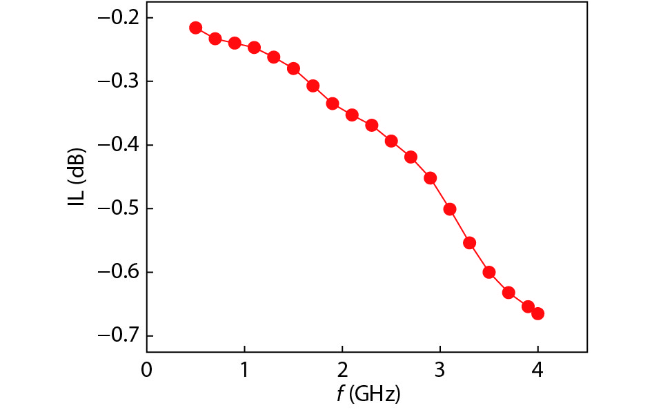
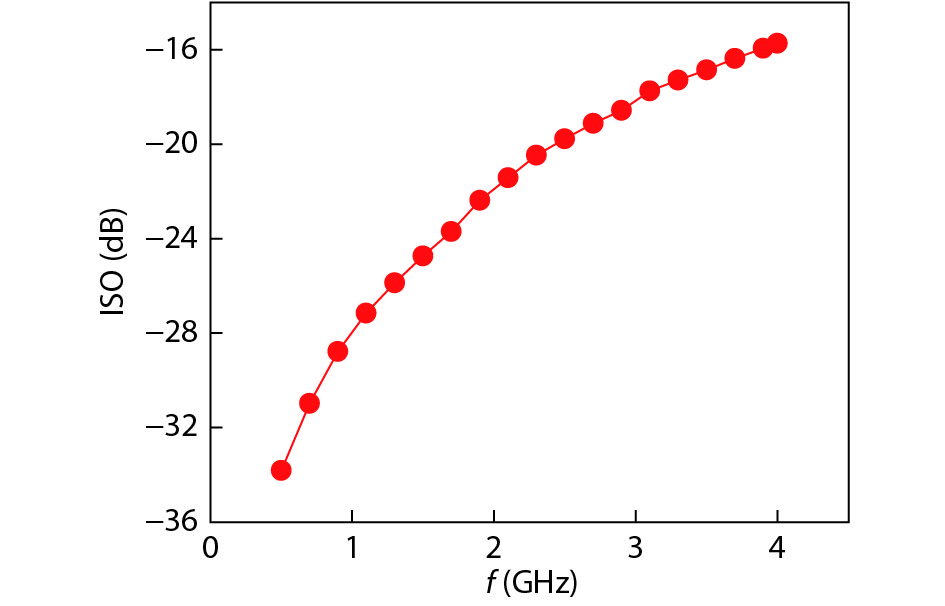
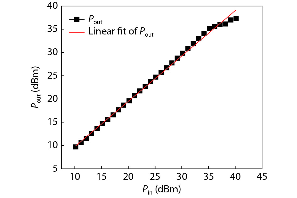
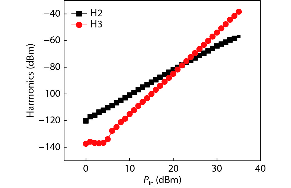
A high-performance single-pole single-throw (SPST) RF switch for mobile phone RF front-end modules (FEMs) was designed and characterized in a 0.13 μm partially depleted silicon-on-insulator (PD SOI) process. In this paper, the traditional series-shunt configuration design was improved by introducing a suitably large DC bias resistor and leakage-preventing PMOS, together with the floating body technique. The performance of the RF switch is greatly improved. Furthermore, a new Ron × Coff testing method is also proposed. The size of this SPST RF switch is 0.2 mm2. This switch can be widely used for present 4G and forthcoming 5G mobile phone FEMs.

J. Semicond.
2019, 40(2): 022402 doi: 10.1088/1674-4926/40/2/022402
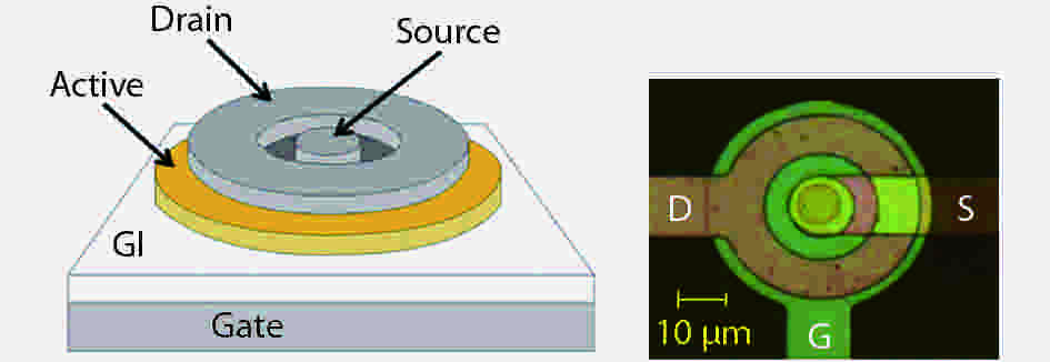
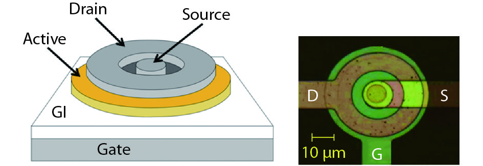
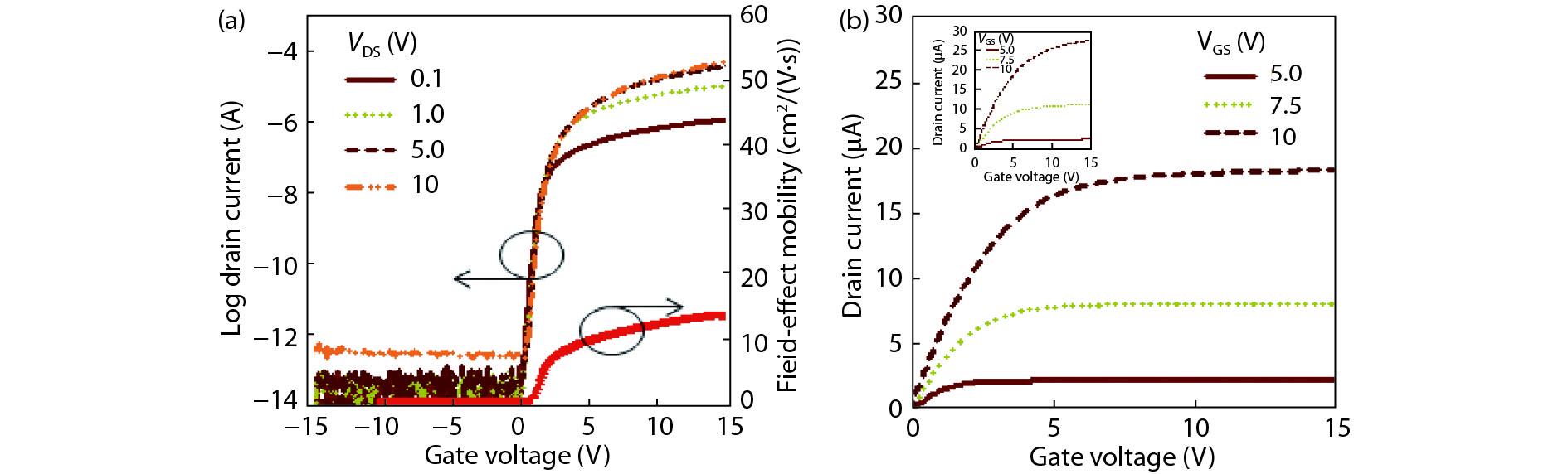
We report a high-performance active image sensor pixel design by utilizing amorphous-indium-gallium-zinc-oxide (a-IGZO) thin-film transistors (TFTs) with a circular structure. The TFT, configured with the inner electrode as source and outer electrode as drain, typically exhibits good saturation electrical characteristics, where the device has a constant drive current despite variations in drain voltage. Due to the very high output resistance exhibited by this asymmetric TFT structure with a circular shape, the pixel circuit considered here in common-drain configuration provides a higher gain of operation than a pixel circuit implemented with rectangular a-IGZO TFTs. They can be used as driving TFTs in active image sensor circuits. They are, therefore, good candidates for digital X-ray detectors in applications such as medical diagnostic procedures.
J. Semicond.
2019, 40(2): 022403 doi: 10.1088/1674-4926/40/2/022403
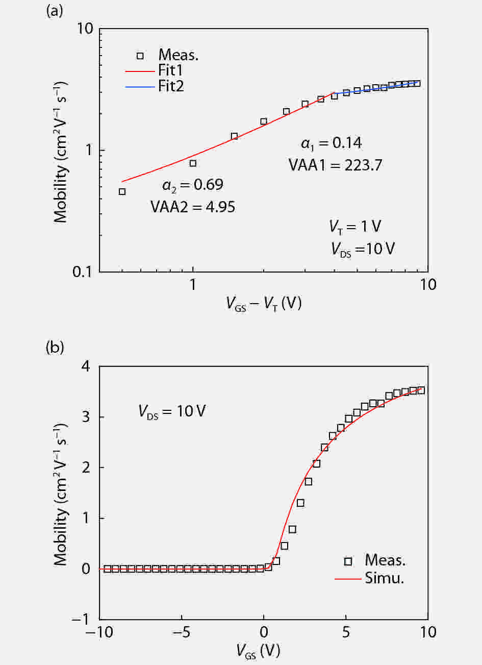
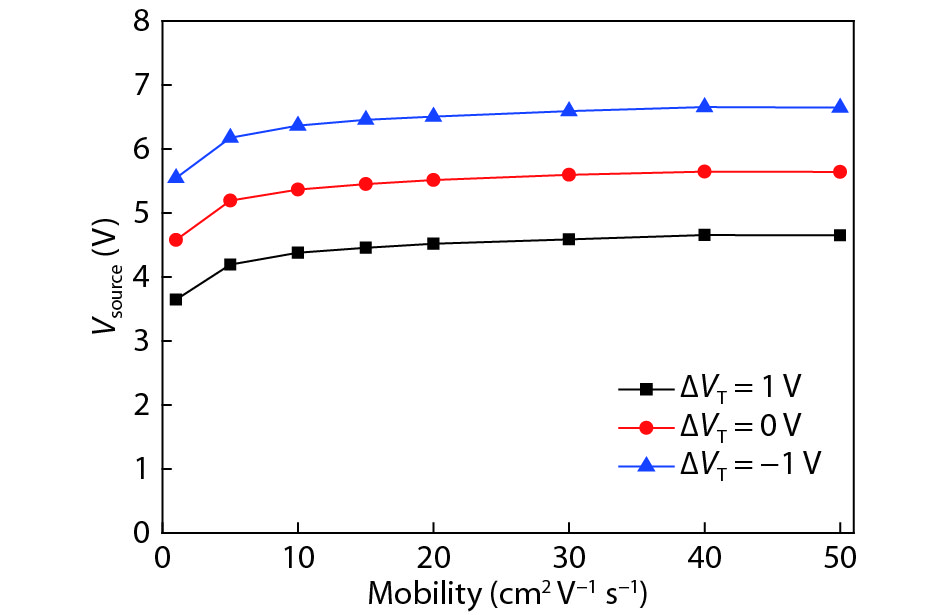
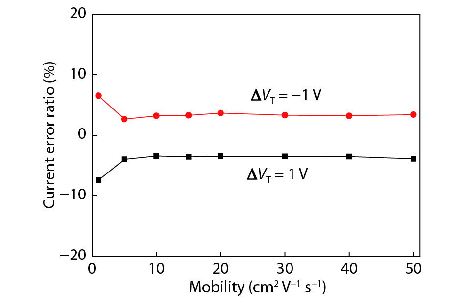
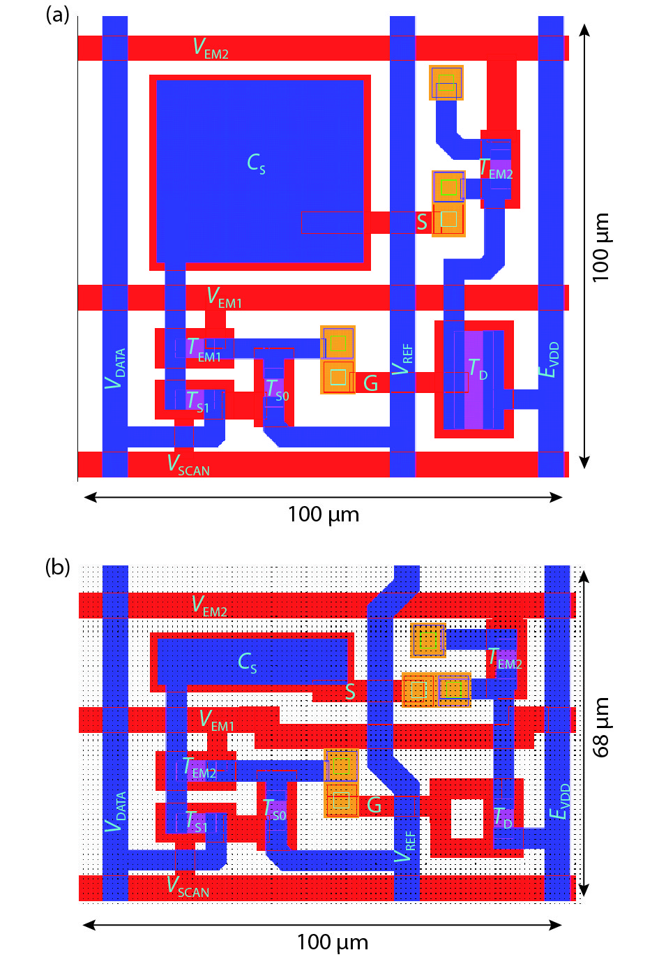
The suitability of indium gallium zinc oxide (IGZO) thin-film transistors (TFT) for implementation of active matrix display of organic light emitting diodes (AMOLED) compensation pixel circuits is addressed in this paper. In particular, the impact of mobility on compensating performance for the implementation in AMOLED pixel circuits is investigated. Details of the effective mobility modeling using the power law of gate-to-source voltage are provided, and parameters are extracted according to the measured current-to-voltage data of IGZO TFT samples. The investigated AMOLED pixel circuit consists of 4 switching TFTs, 1 driving TFT, and 1 capacitor. A " source-follower” structure is used for the threshold voltage extraction of the driving transistor. A new timing diagram is proposed; thus the current error of the pixel circuit is almost independent of the effective mobility. But, to improve the precision of the threshold voltage extraction of the driving transistor, the mobility is required to be greater than 5 cm2V−1s−1. On the other hand, the optimized storage capacitance is reversely proportional to the effective mobility. Thus, the layout area of the pixel circuit can be decreased from 100 × 100 to 100 × 68 μm2, with the effective mobility increased from 10 to 50 cm2V−1s−1. Therefore, IGZO TFT is a good alternative backplane technology for AMOLED displays, and a higher effective mobility is preferred for high compensation performance and compact layout.

J. Semicond.
2019, 40(2): 022801 doi: 10.1088/1674-4926/40/2/022801
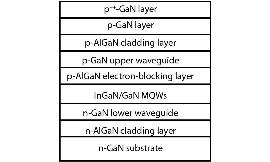
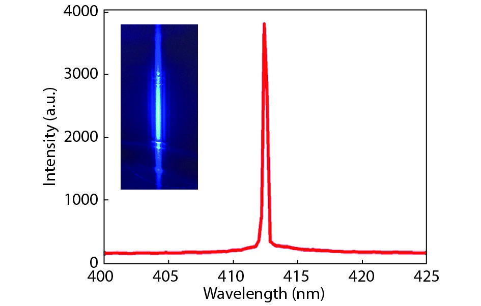
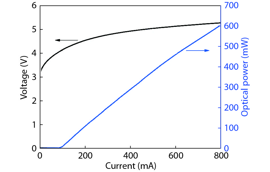
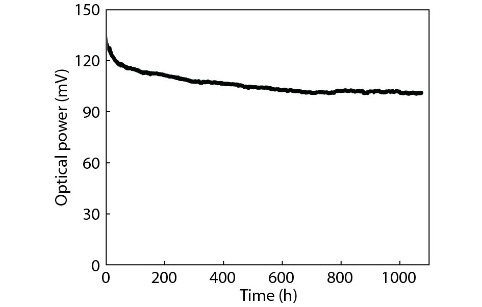
GaN-based continuous-wave operated blue-violet laser diodes (LDs) with long lifetime are demonstrated, which are grown on a c-plane GaN substrate by metal organic chemical vapor deposition with a 10 × 600 μm2 ridge waveguide structure. The electrical and optical characteristics of a blue-violet LD are investigated under direct-current injection at room temperature (25 °C). The stimulated emission wavelength and peak optical power of the LD are around 413 nm and over 600 mW, respectively. In addition, the threshold current density and voltage are as small as 1.46 kA/cm2 and 4.1 V, respectively. Moreover, the lifetime is longer than 1000 hours under room-temperature continuous-wave operation.
J. Semicond.
2019, 40(2): 022802 doi: 10.1088/1674-4926/40/2/022802
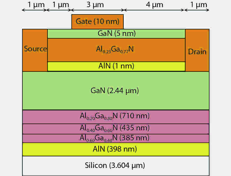
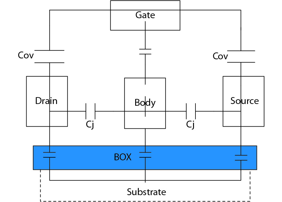
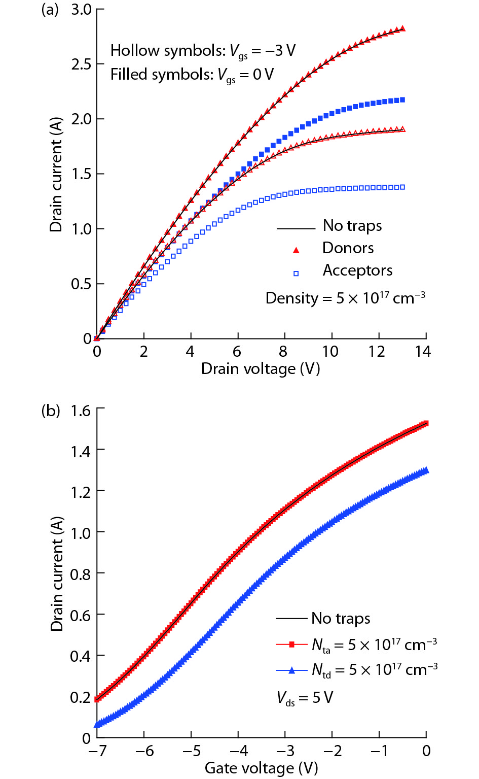
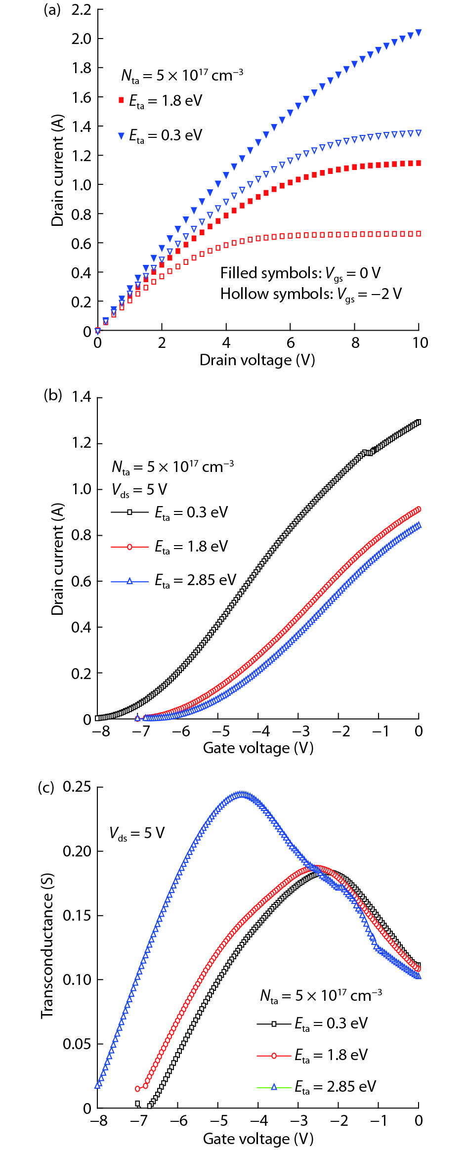
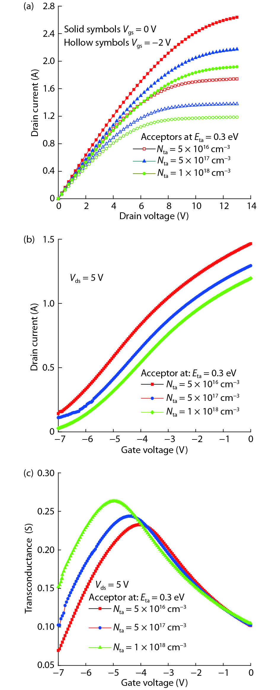
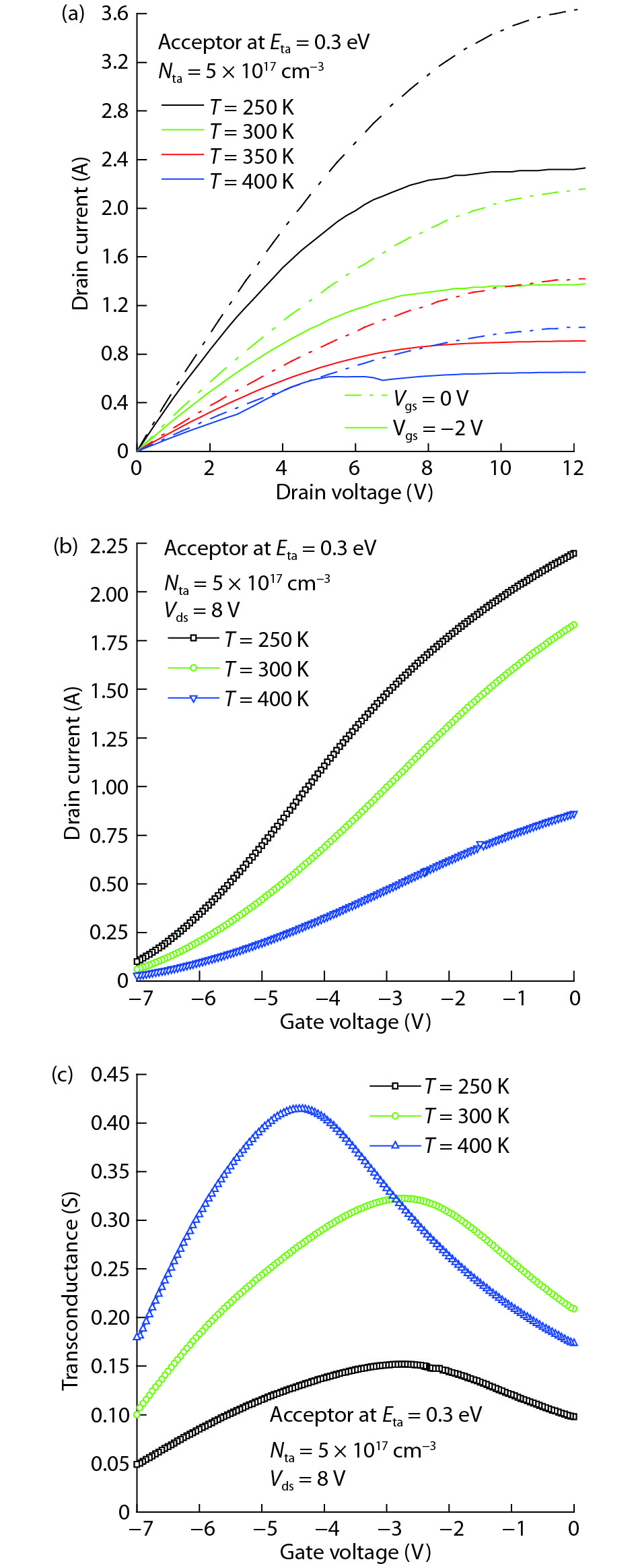
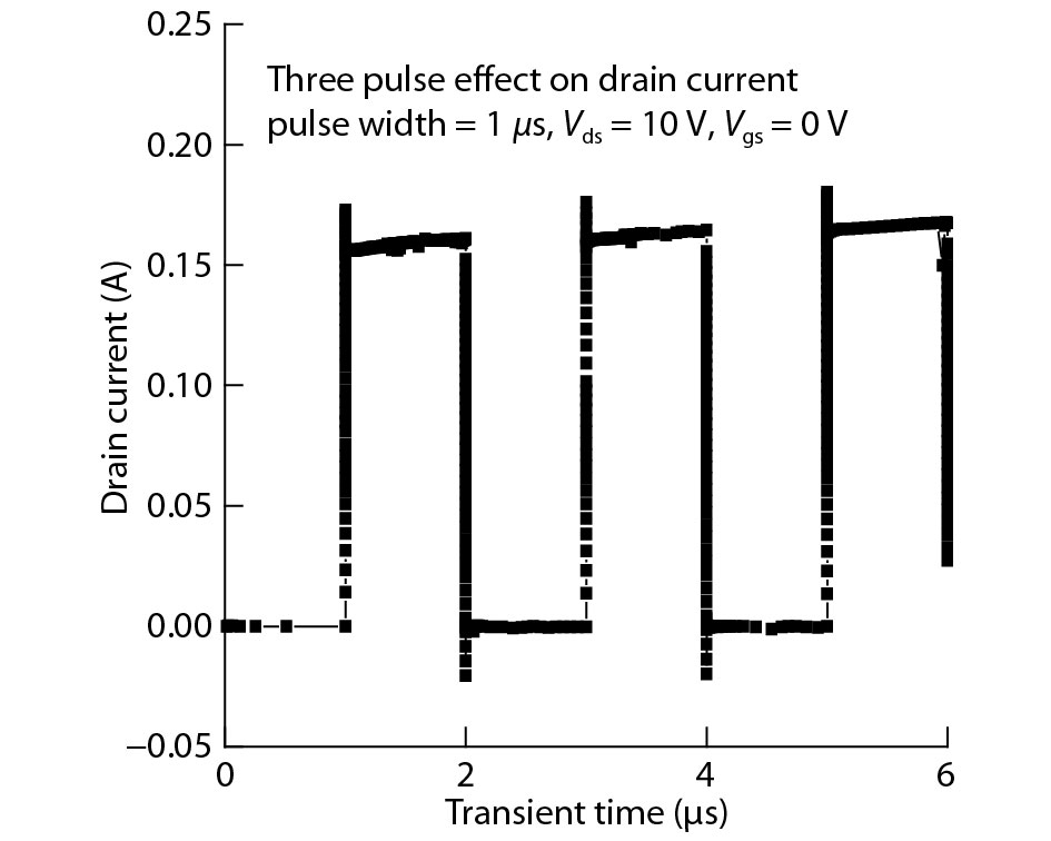
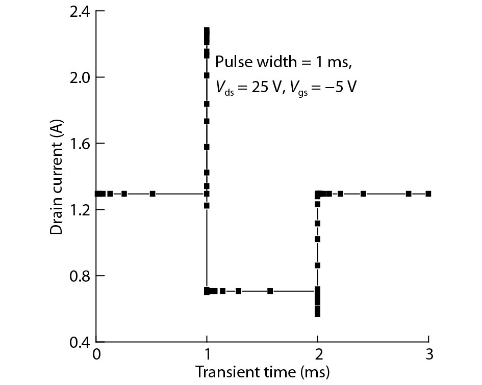
In this work, the effects of GaN channel traps and temperature on the performance of AlGaN/AlN/GaN/AlGaN high electron mobility transistors (HEMTs) on Si (111) substrate, were investigated. 2D simulations carried out using the Silvaco TCAD simulator tool for different drain and gate voltages showed that acceptor-like traps in the channel have a significant influence on the DC and RF characteristics. It was found that deeper acceptors below the conduction band with larger concentration have a more pronounced effect on the transistor performance. Meanwhile, the donor-like traps show no influence. Pulsing the device with different pulse widths and bias conditions, as well as increasing temperature, showed that the traps are more ionized when the pulse is wider or the temperature is higher, which can degrade the drain current and thus the DC characteristics of the transistor. Passivation of the transistor has also a beneficial effect on performance.

J. Semicond.
2019, 40(2): 022803 doi: 10.1088/1674-4926/40/2/022803
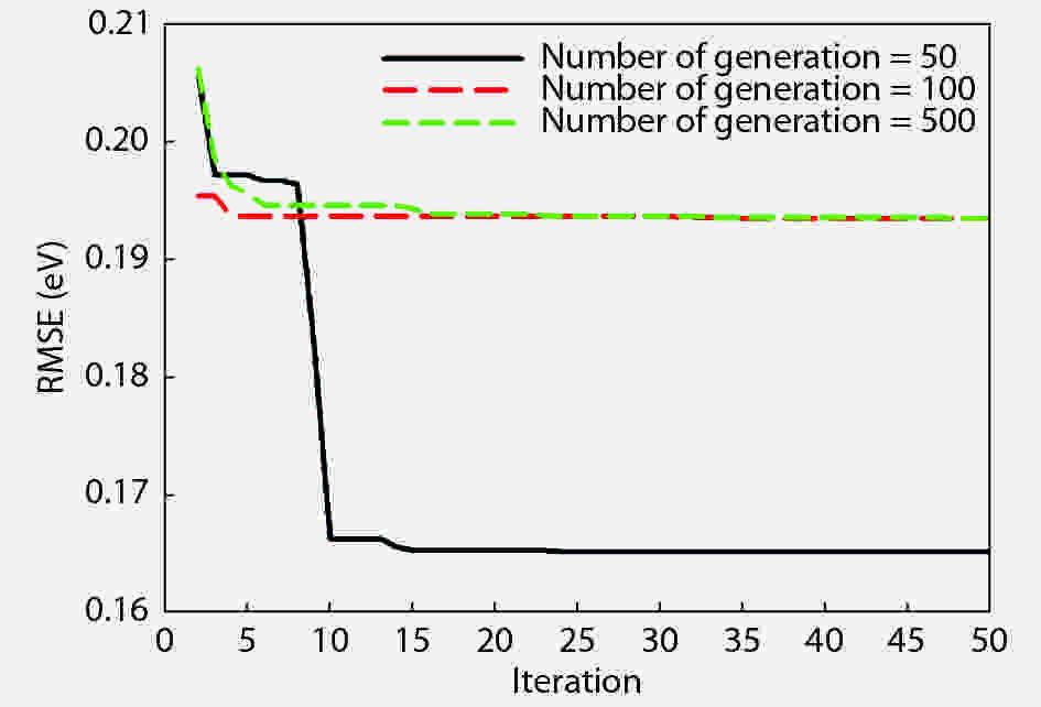
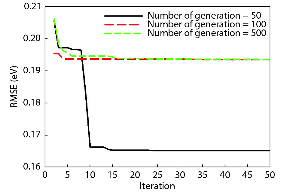
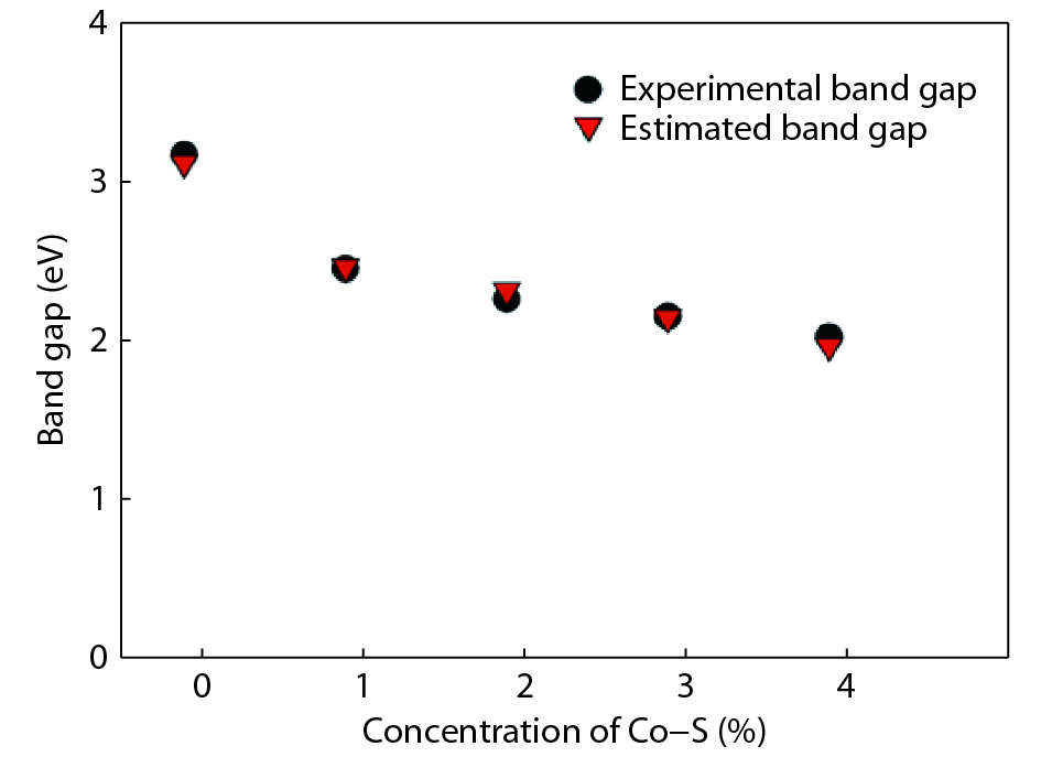
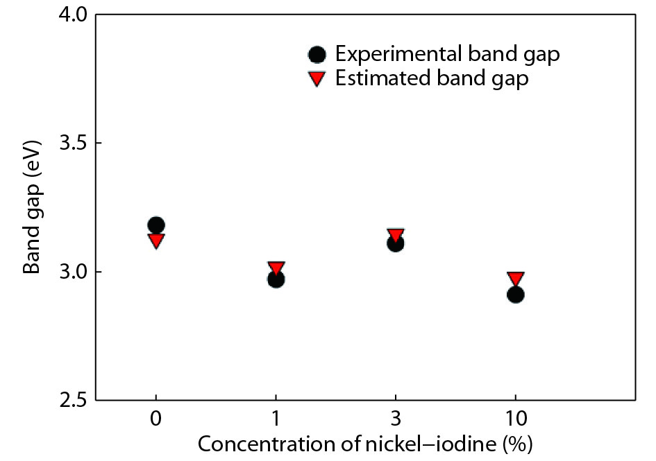
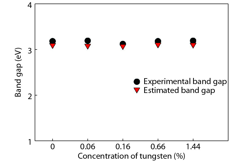
Energy band gap of titanium dioxide (TiO2) semiconductor plays significant roles in many practical applications of the semiconductor and determines its appropriateness in technological and industrial applications such as UV absorption, pigment, photo-catalysis, pollution control systems and solar cells among others. Substitution of impurities into crystal lattice structure is the most commonly used method of tuning the band gap of TiO2 for specific application and eventually leads to lattice distortion. This work utilizes the distortion in the lattice structure to estimate the band gap of doped TiO2, for the first time, through hybridization of a particle swarm optimization algorithm (PSO) with a support vector regression (SVR) algorithm for developing a PSO-SVR model. The precision and accuracy of the developed PSO-SVR model was further justified by applying the model for estimating the effect of cobalt-sulfur co-doping, nickel-iodine co-doping, tungsten and indium doping on the band gap of TiO2 and excellent agreement with the experimentally reported values was achieved. Practical implementation of the proposed PSO-SVR model would further widen the applications of the semiconductor and reduce the experimental stress involved in band gap determination of TiO2.


J. Semicond.
2019, 40(2): 022804 doi: 10.1088/1674-4926/40/2/022804
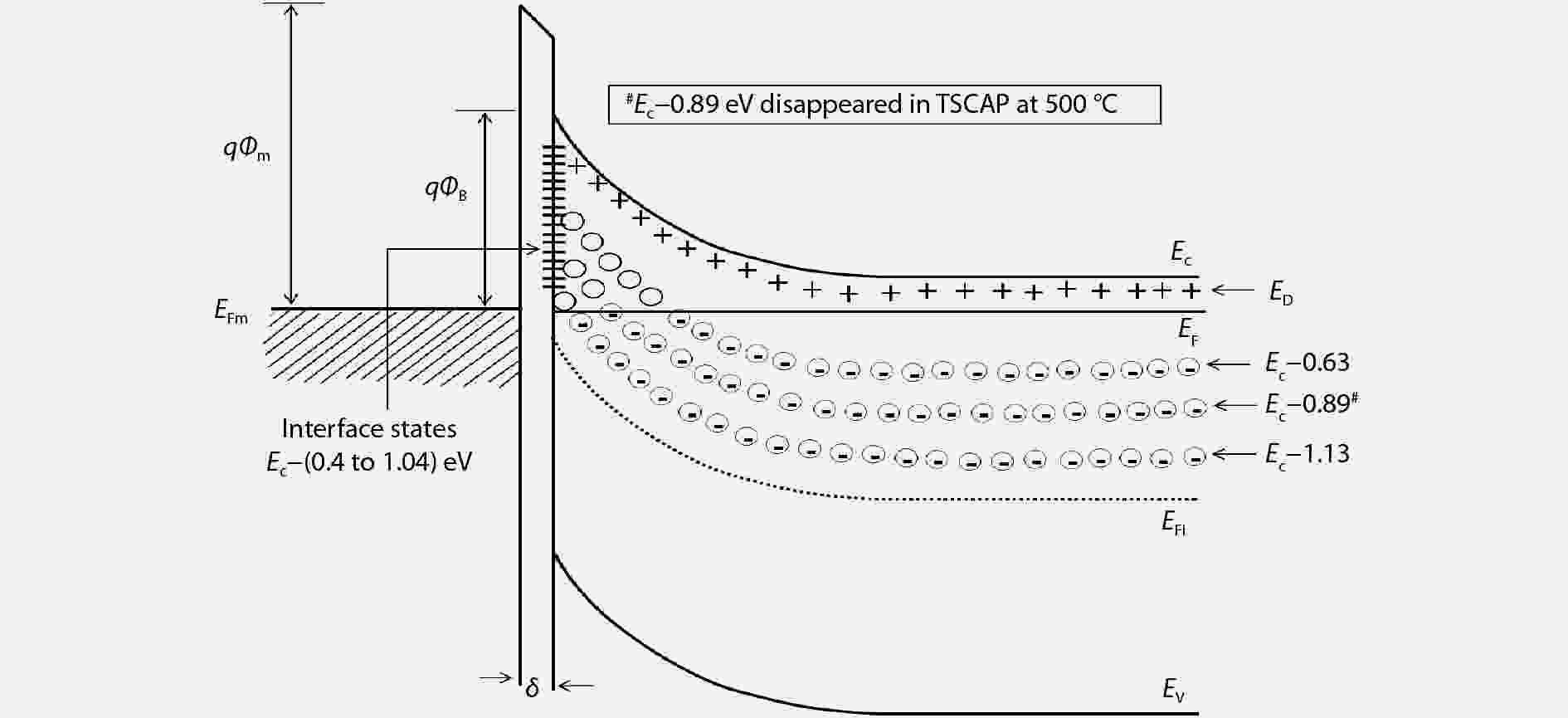
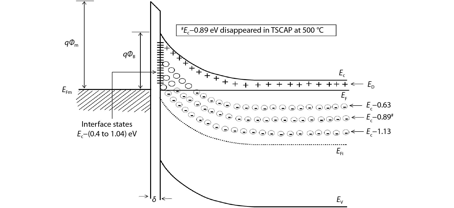
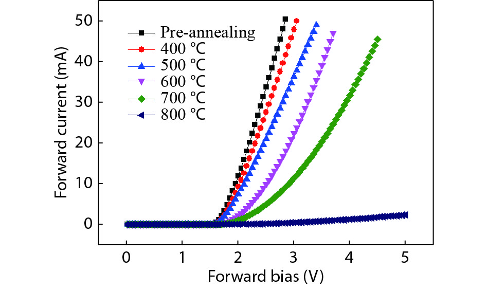
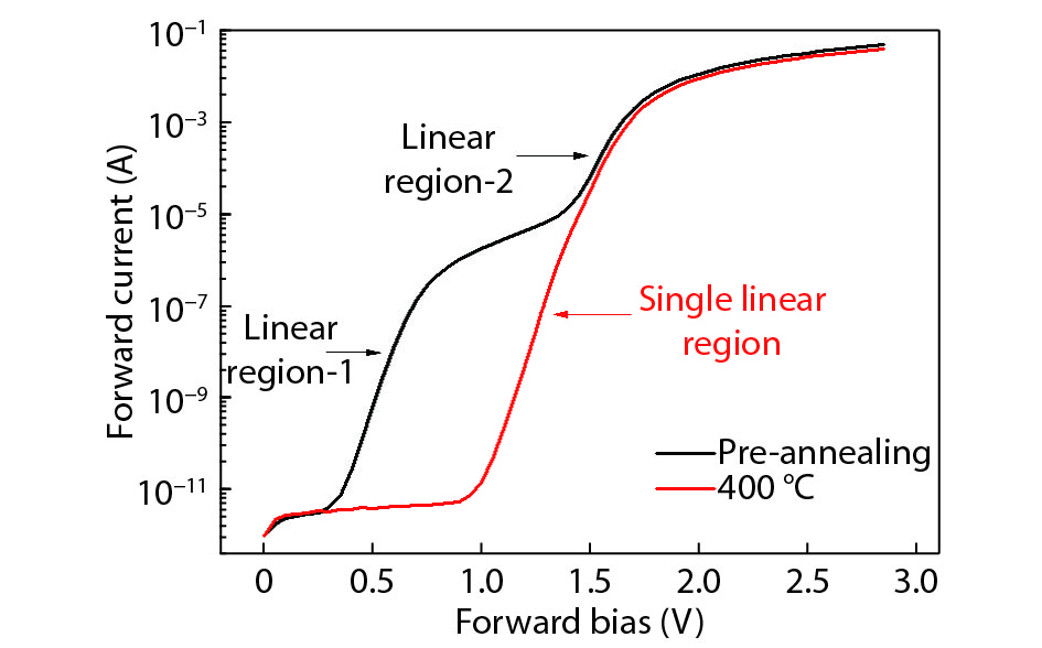
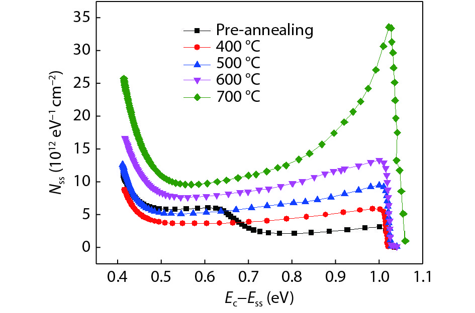
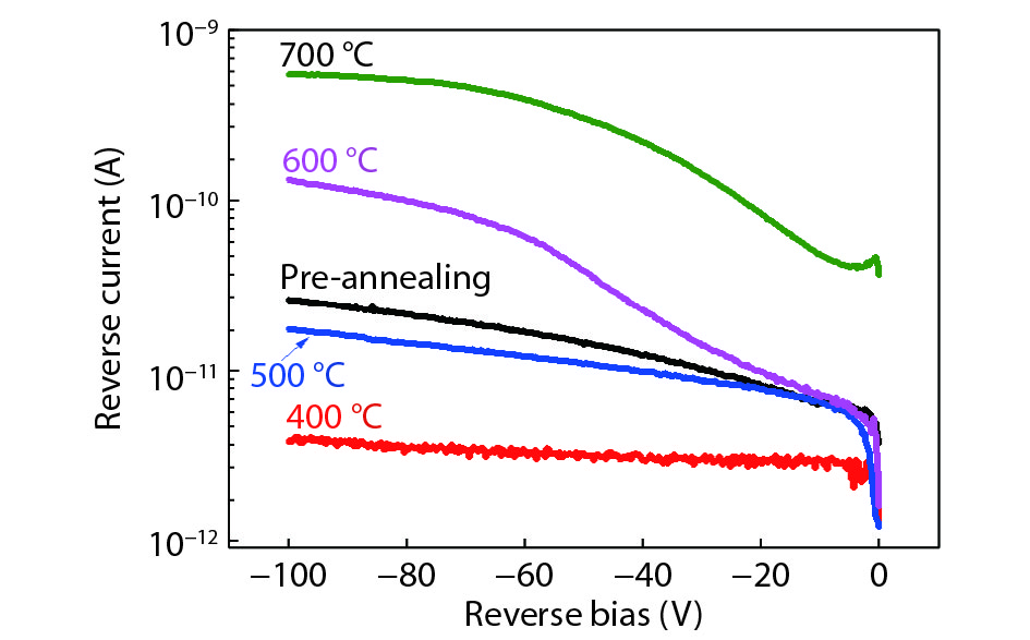
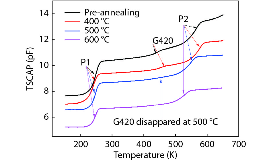
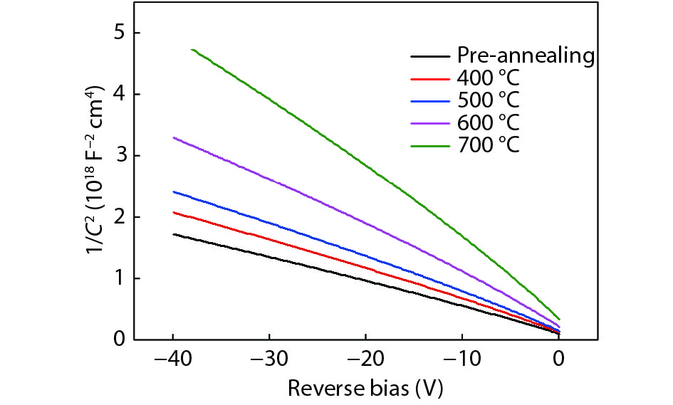
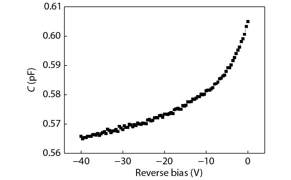
Thermal annealing effects on gamma irradiated Ni/4H-SiC Schottky barrier diode (SBD) characteristics are analyzed over a wide range of temperatures (400–1100 °C). The annealing induced variations in the concentration of deep level traps in the SBDs are identified by thermally stimulated capacitance (TSCAP). A little decrease in the trap density at EC – 0.63 eV and EC – 1.13 eV is observed up to the annealing temperature of 600 °C. Whereas, a gamma induced trap at EC – 0.89 eV disappeared after annealing at 500 °C, revealing that its concentration (< 1013 cm−3) is reduced below the detection limit of the TSCAP technique. The electrical characteristics of irradiated SBDs are considerably changed at each annealing temperature. To understand the anomalous variations in the post-annealing characteristics, the interface state density distribution in the annealed SBDs is extracted. The electrical properties are improved at 400 °C due to the reduction in the interface trap density. However, from 500 °C, the electrical parameters are found to degrade with the annealing temperature because of the increase in the interface trap density. From the results, it is noted that the rectifying nature of the SBDs vanishes at or above 800 °C.