Issue Browser
Volume 40, Issue 3,
Mar 2019

J. Semicond.
2019, 40(3): 032101 doi: 10.1088/1674-4926/40/3/032101
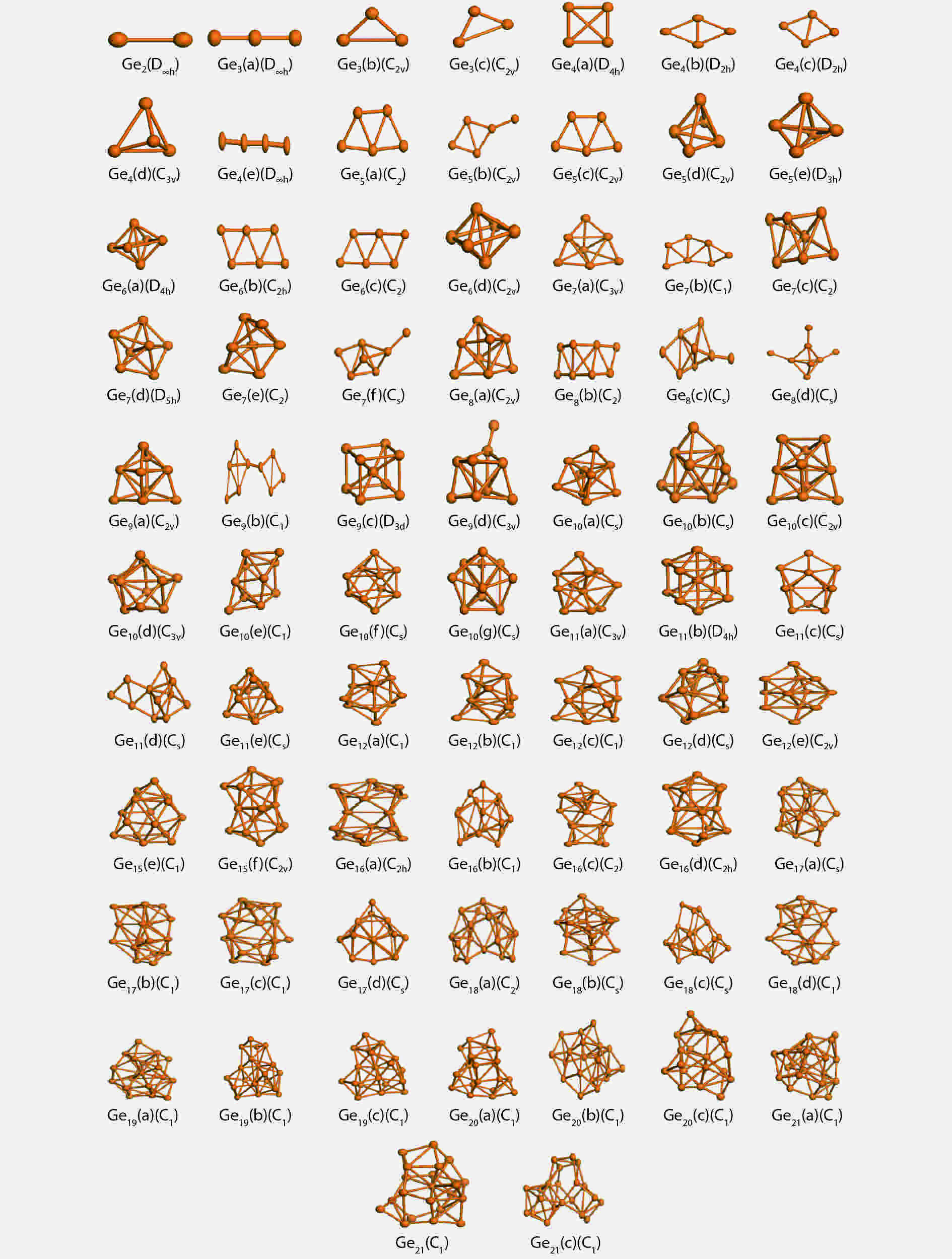
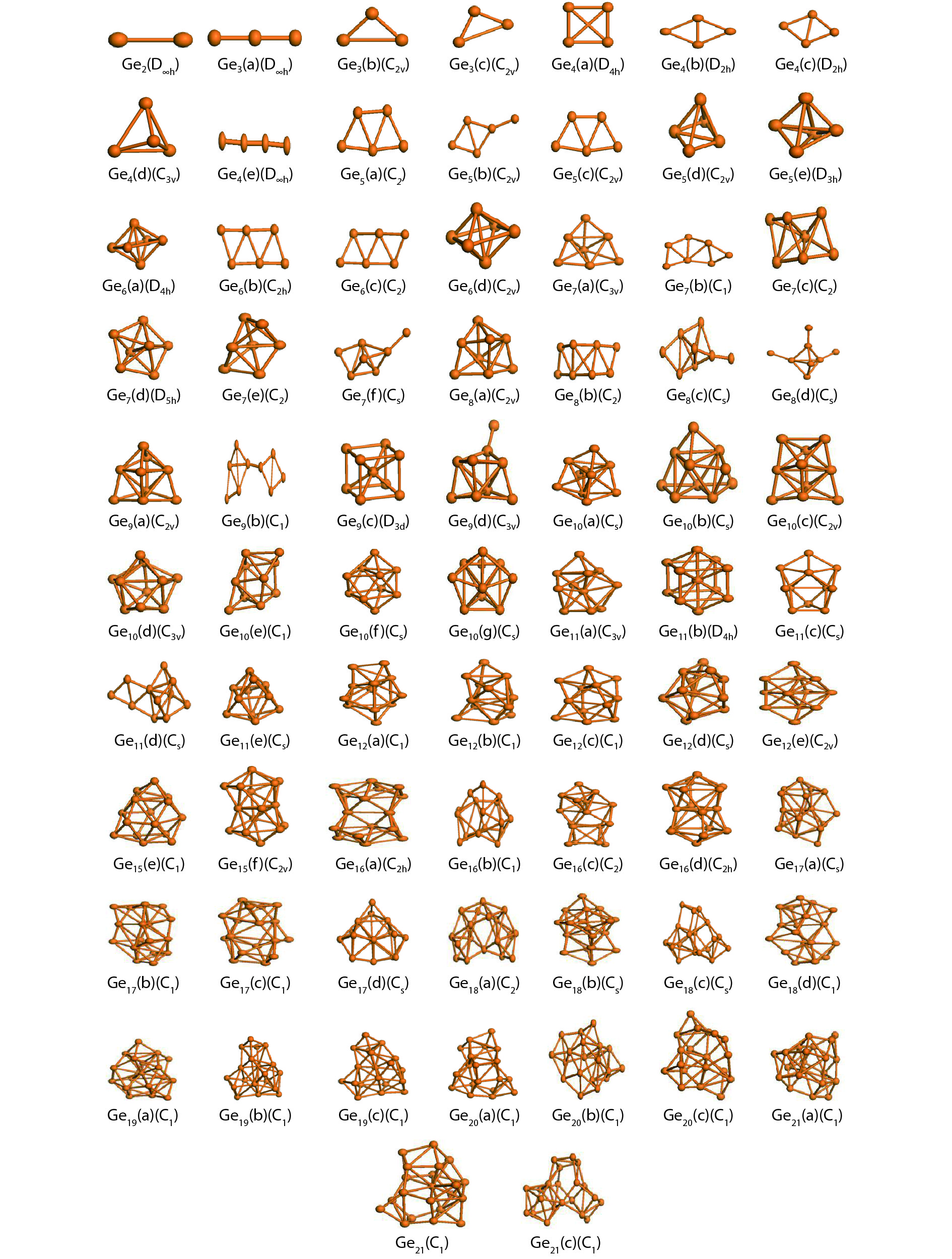
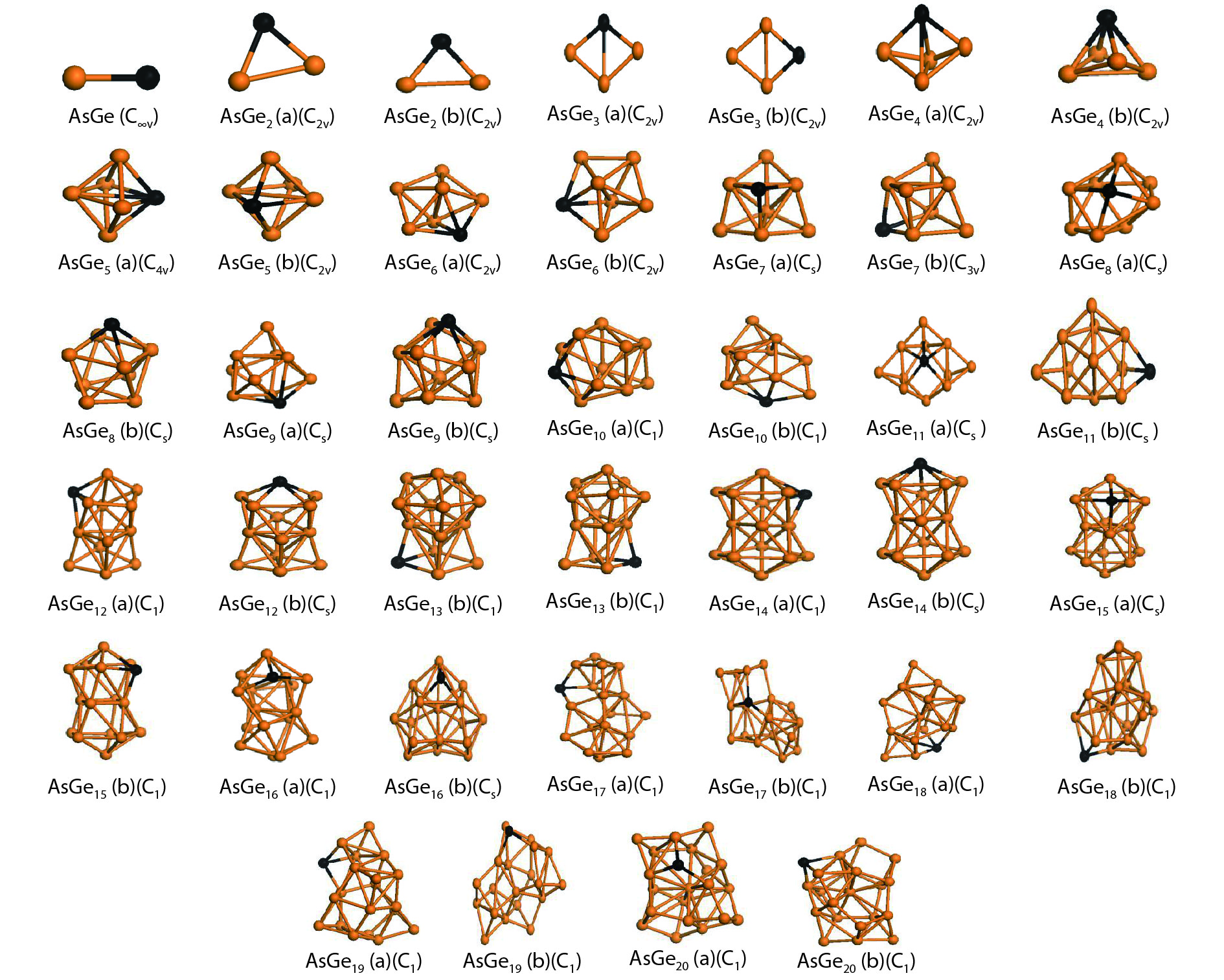
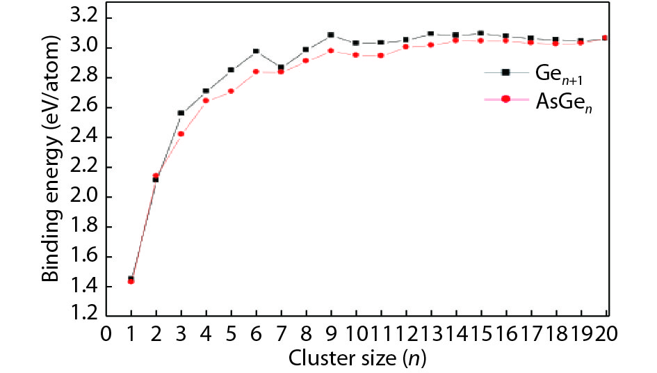
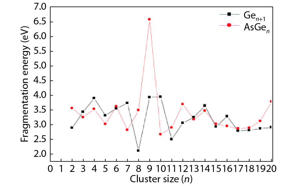
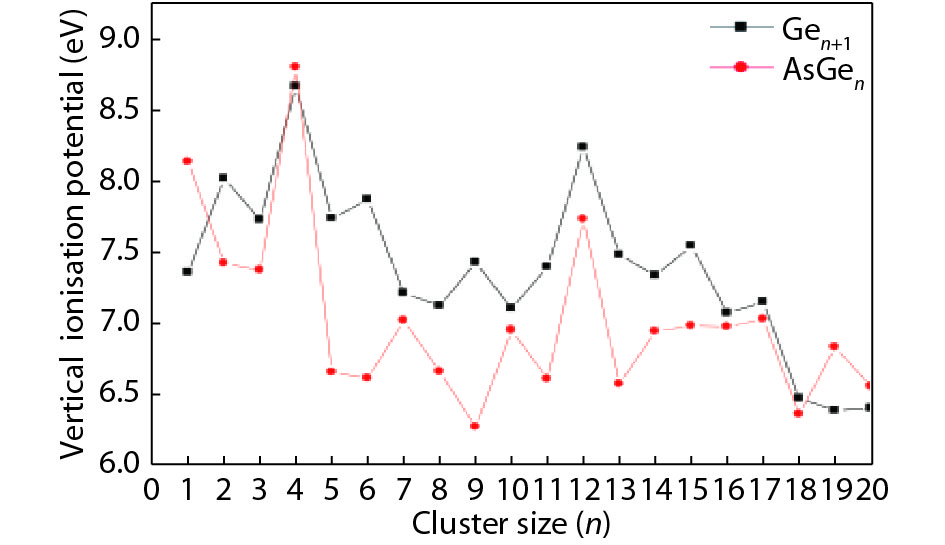
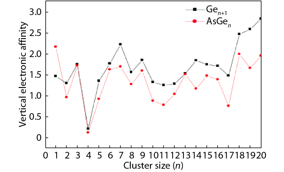
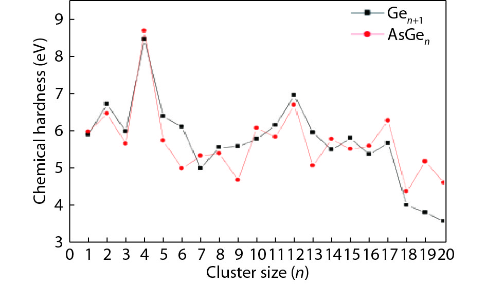
We present a systematic computational study based on the density functional theory (DFT) aiming to high light the possible effects of one As doping atom on the structural, energetic, and electronic properties of different isomers of Gen + 1 clusters with n = 1–20 atoms. By considering a large number of structures for each cluster size, the lowest-energy isomers are determined. The lowest-energy isomers reveal three-dimensional structures starting from n = 5. Their relative stability versus atomic size is examined based on the calculated binding energy, fragmentation energy, and second-order difference of energy. Doping Gen + 1 clusters with one As atom does not improve their stability. The electronic properties as a function of the atomic size are also discussed from the calculated HOMO–LUMO energy gap, vertical ionization potential, vertical electron affinity, and chemical hardness. The obtained results are significantly affected by the inclusion of one As atom into a Gen cluster.


J. Semicond.
2019, 40(3): 032201 doi: 10.1088/1674-4926/40/3/032201
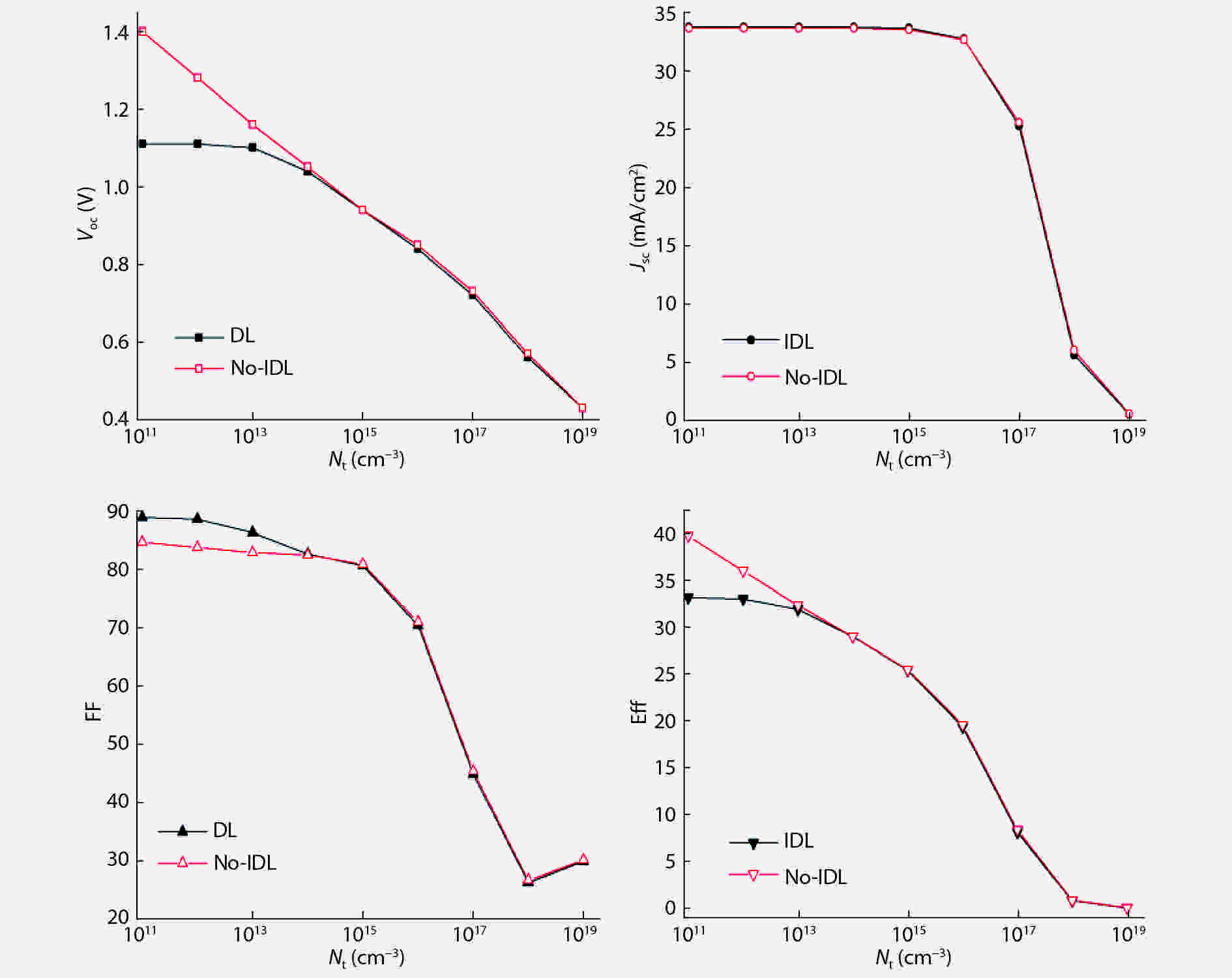
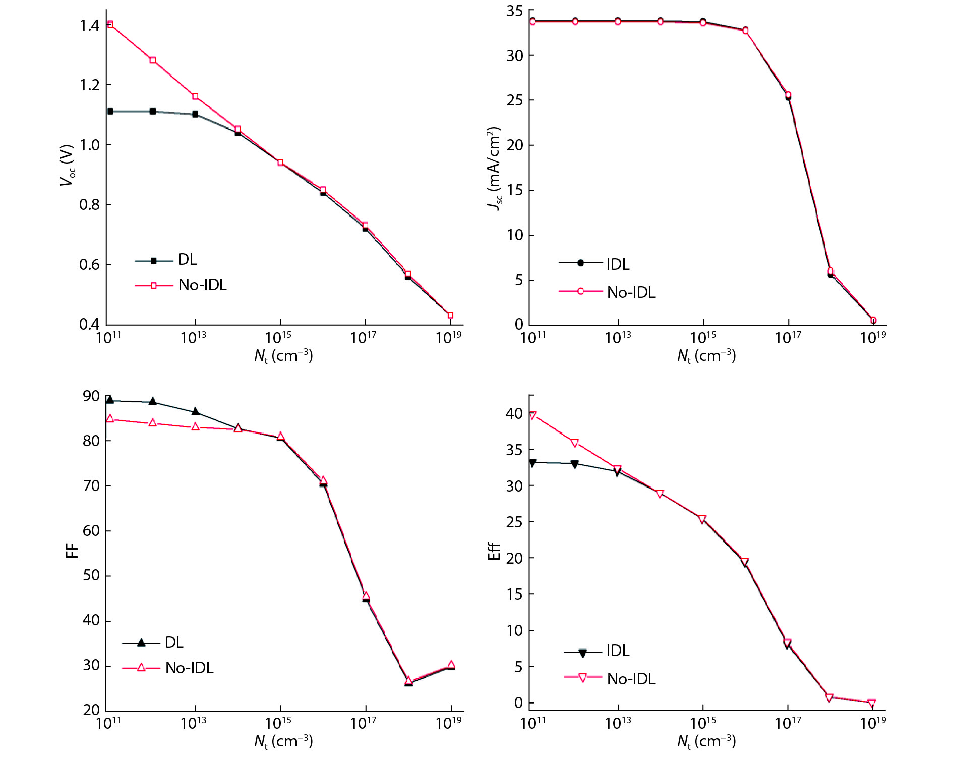
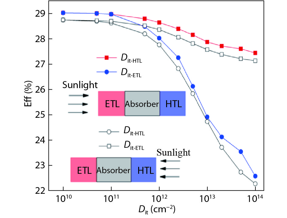
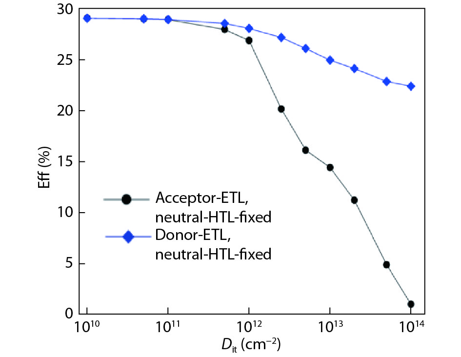
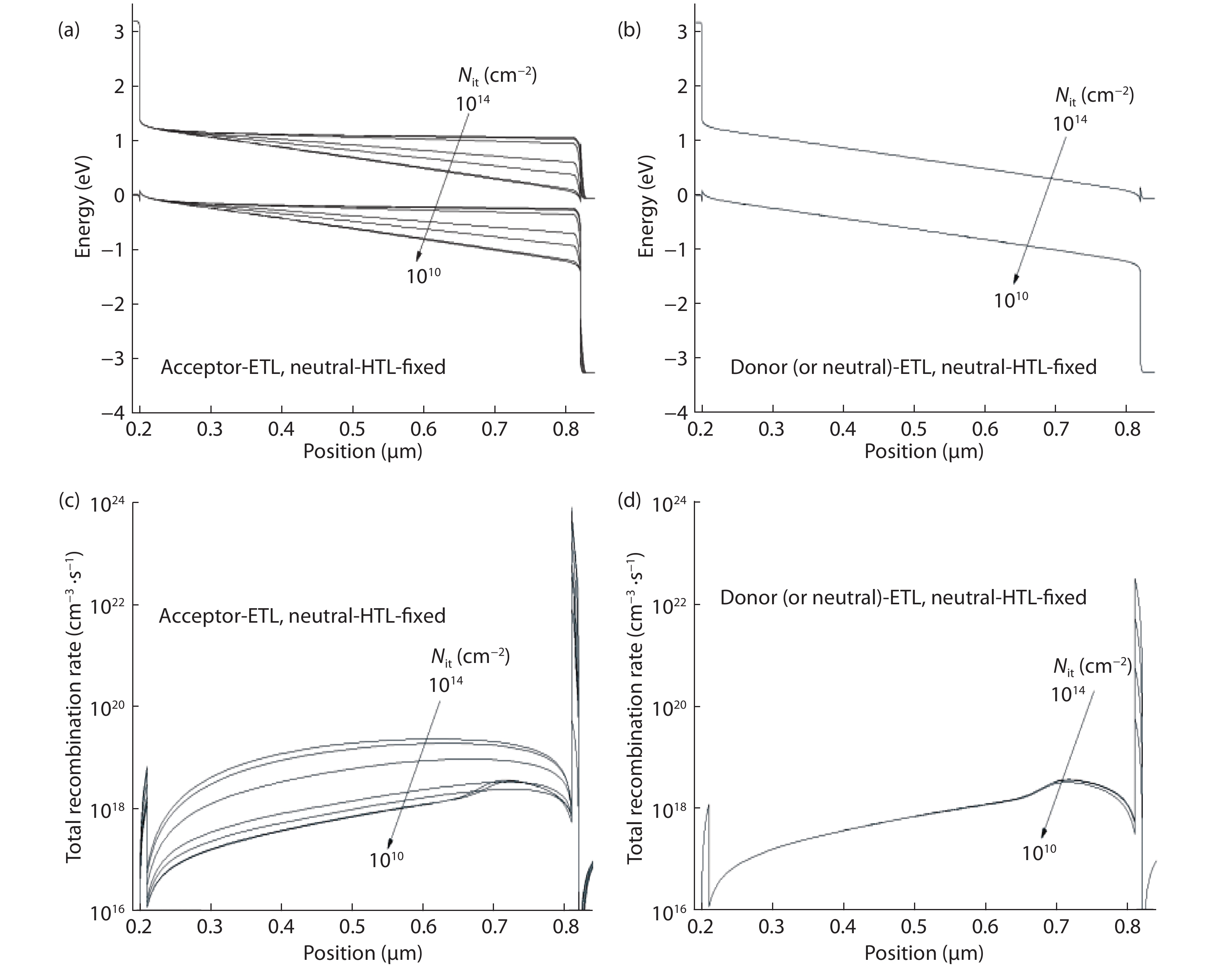
Although tin halide perovskite has shown excellent photoelectric performance, its efficiency of solar cell is low compared with that of lead halide. In order to enhance the efficiency of tin halide perovskite solar cell, a deep understanding of the role of the defects in the perovskite absorption layer and at the electron transport layer (ETL)/absorber or absorber/hole transport layer (HTL) interface is very necessary. In this work, the planar heterojunction-based CH3NH3SnI3 perovskite solar cells were simulated with the SCAPS-1D program. Simulation results revealed a great dependence of device efficiency on defect density and interface quality of the perovskite absorber. The defect density at the front interface is critical for high efficiency, and the polarity of the interface charge has a different impact on the device efficiency. Strikingly, an efficiency over 29% was obtained under the moderate simulation conditions.
J. Semicond.
2019, 40(3): 032301 doi: 10.1088/1674-4926/40/3/032301
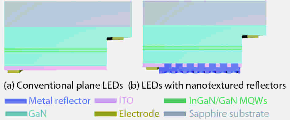
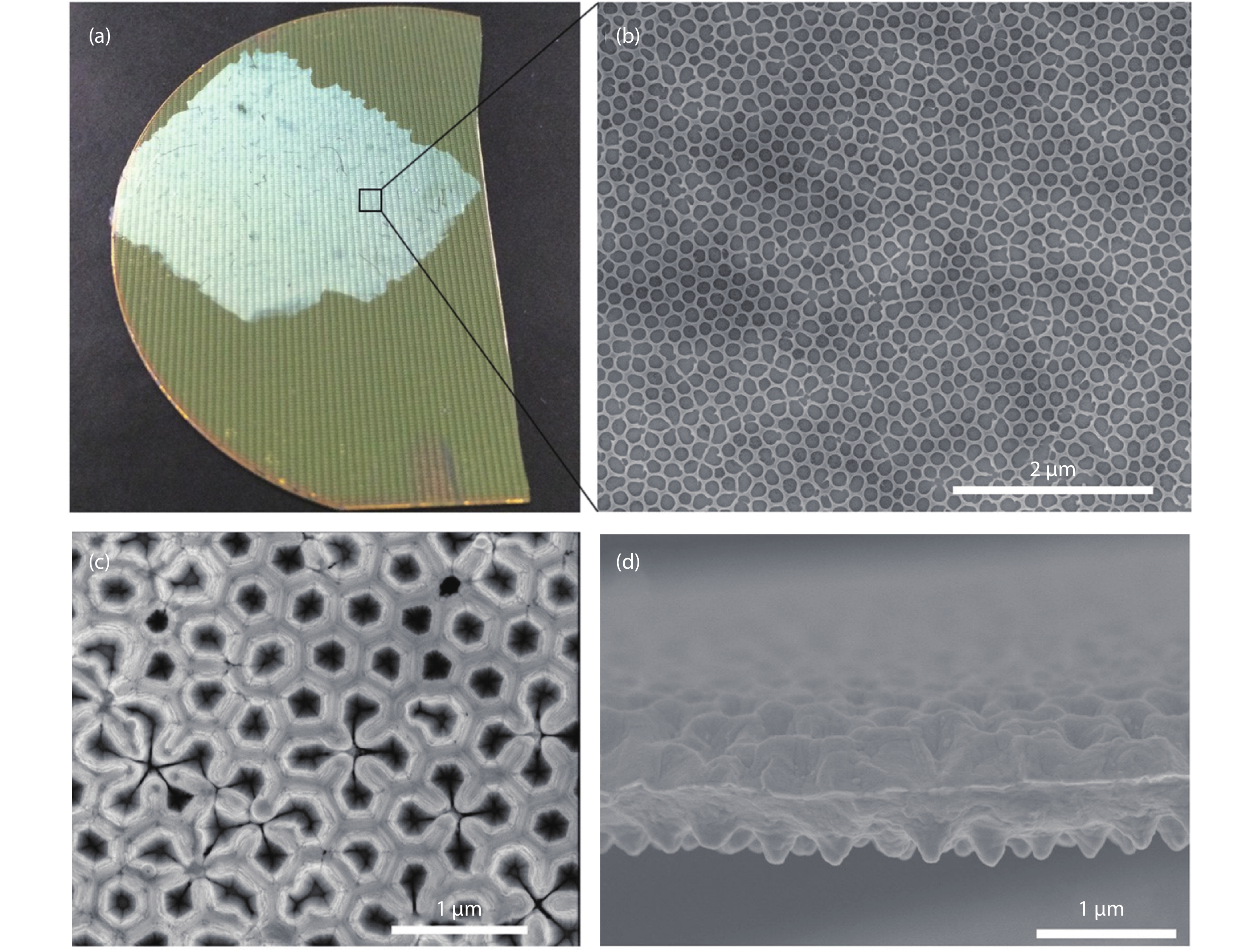
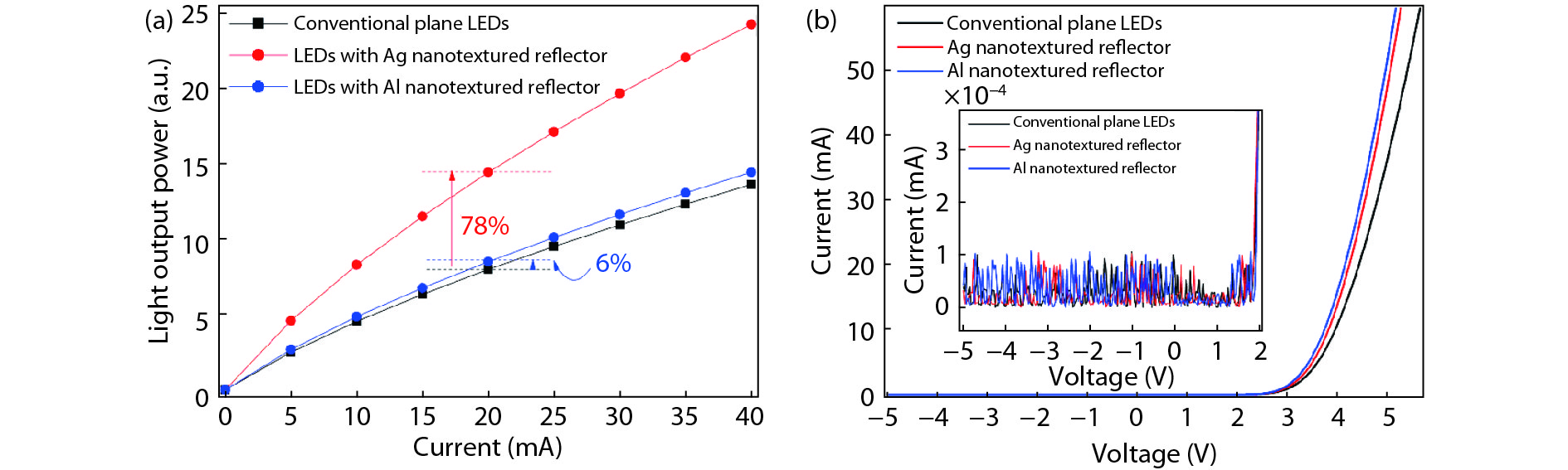
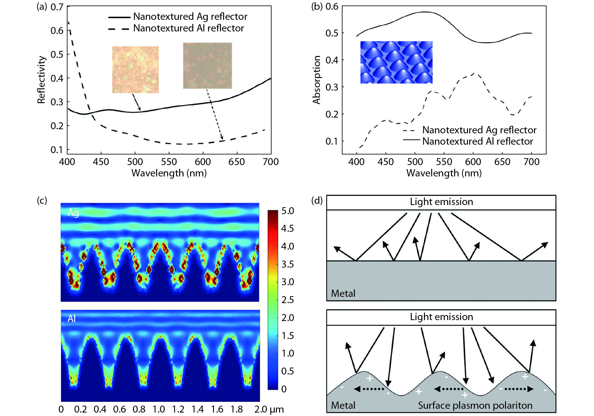
Metallic nanotextured reflectors have been widely used in light emitting diodes (LEDs) to enhance the light extraction efficiency. However, the light absorption loss for the metallic reflectors with nanotexture structure is often neglected. Here, the influence of absorption loss of metallic nanotextured reflectors on the LED optoelectronic properties were studied. Two commonly used metal reflectors Ag and Al were applied to green GaN-based LEDs. By applying a Ag nanotextured reflector, the light output power of the LEDs was enhanced by 78% due to the improved light extraction. For an Al nanotextured reflector, however, only a 6% enhancement of the light output power was achieved. By analyzing the metal absorption using finite-difference time-domain (FDTD) and the metal reflectivity spectrum, it is shown that the surface plasmon (SP) intrinsic absorption of metallic reflectors with nanotexture structure play an important role. This finding will aid the design of the high-performance metal nanotextured reflectors and optoelectronics devices.
J. Semicond.
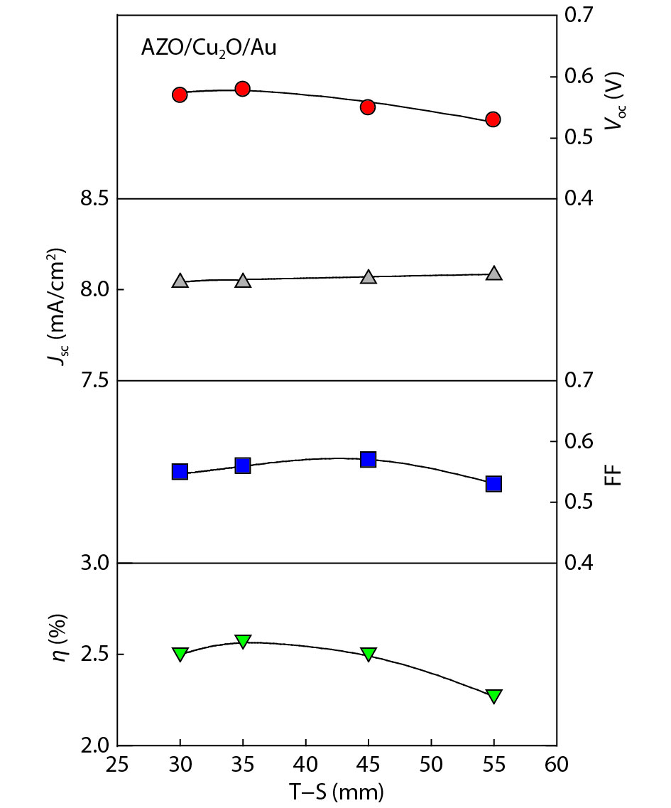
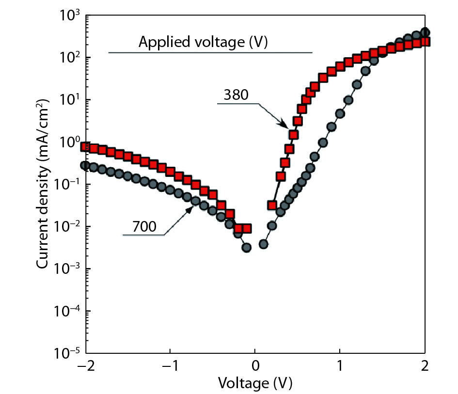
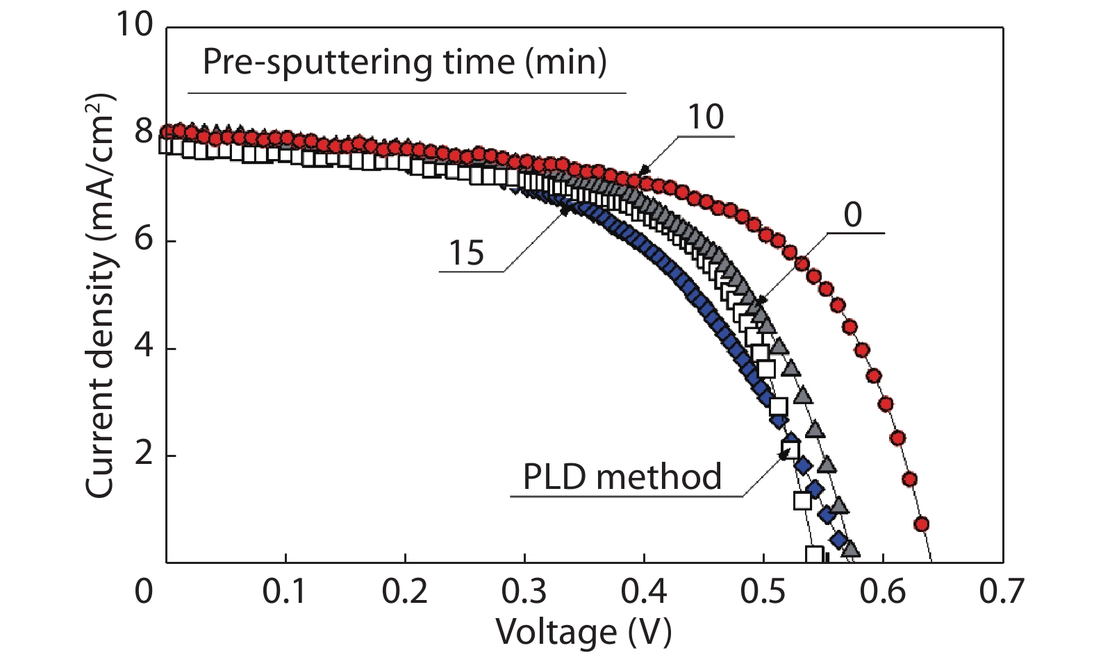
2019, 40(3): 032701 doi: 10.1088/1674-4926/40/3/032701
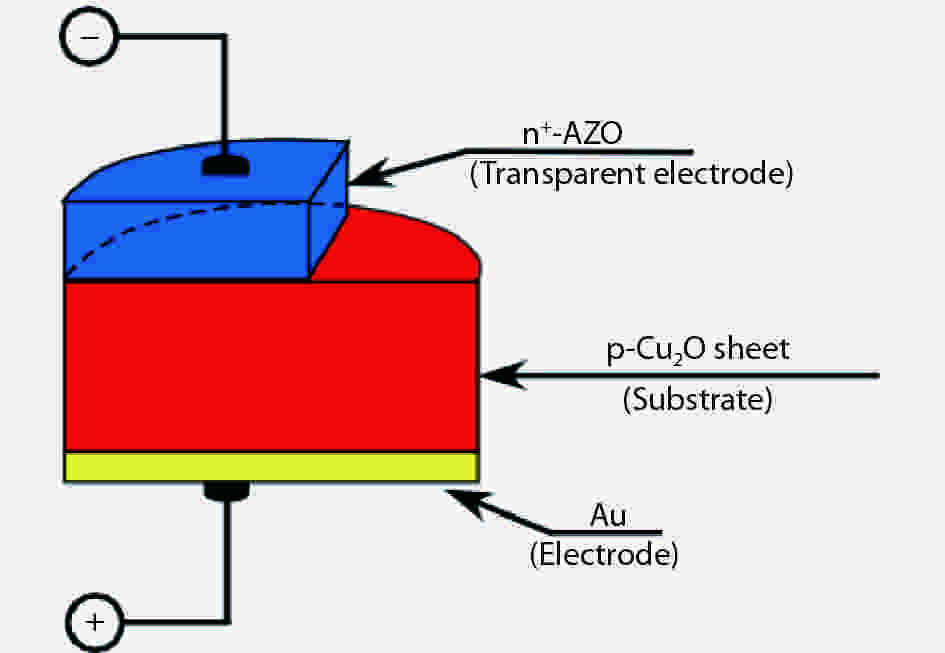
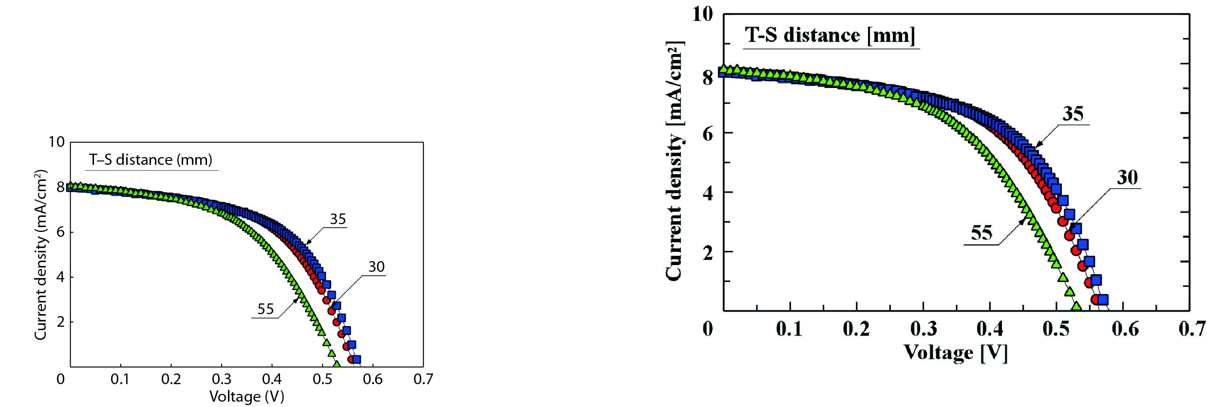
We improved the photovoltaic properties of Cu2O-based heterojunction solar cells using n-type oxide semiconductor thin films prepared by a sputtering apparatus with our newly developed multi-chamber system. We also obtained the highest efficiency (3.21%) in an AZO/p-Cu2O heterojunction solar cell prepared with optimized pre-sputtering conditions using our newly developed multi-chamber sputtering system. This value achieves the same or higher characteristics than AZO/Cu2O solar cells with a similar structure prepared by the pulse laser deposition method.

J. Semicond.
2019, 40(3): 032702 doi: 10.1088/1674-4926/40/3/032702
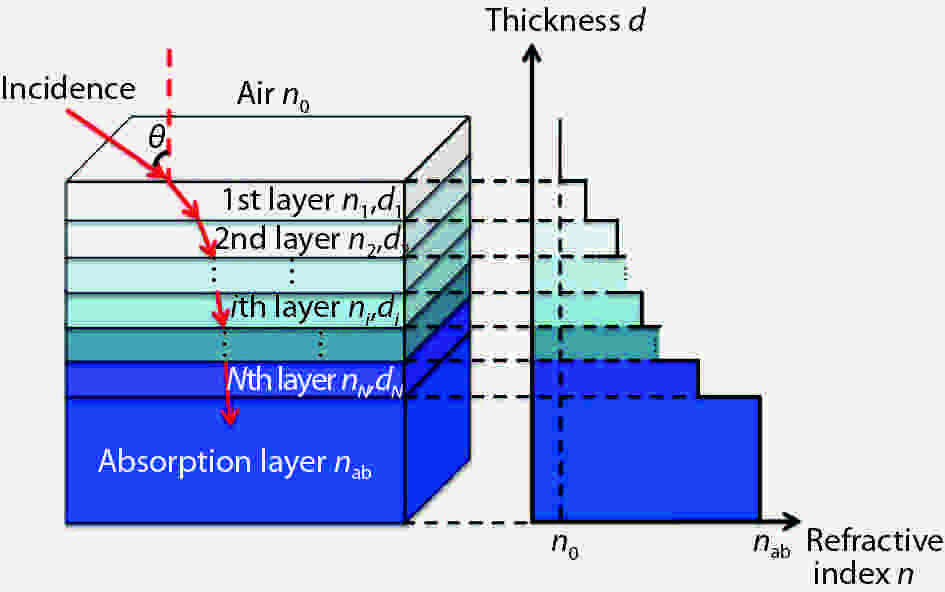
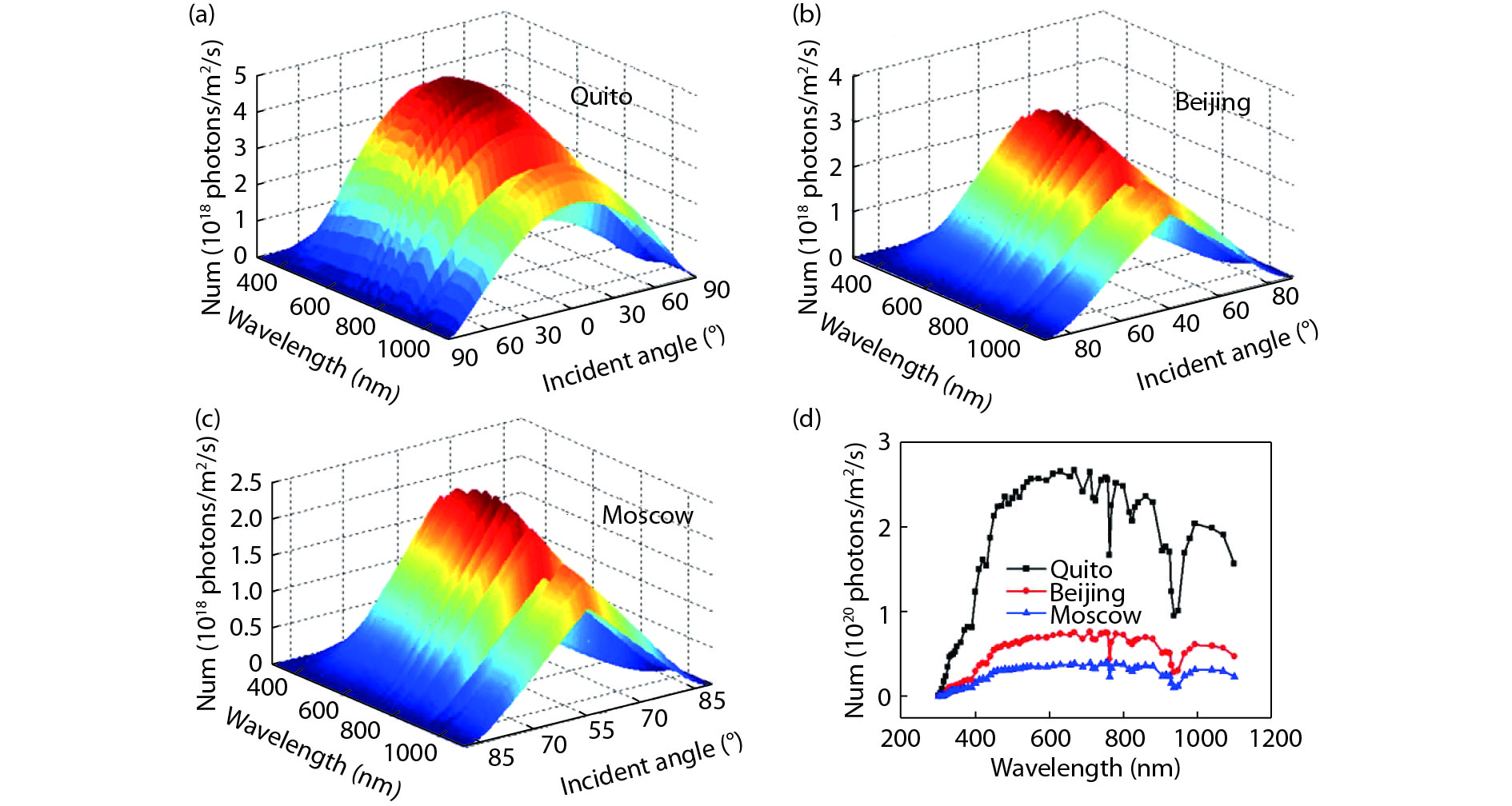
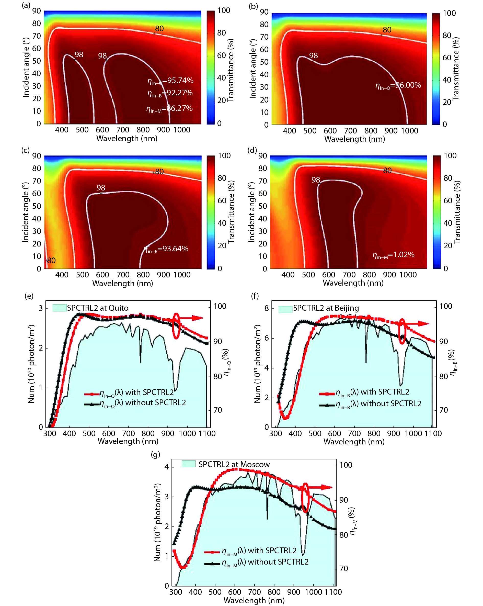
Broadband and omnidirectional antireflection coating is generally an effective way to improve solar cell efficiency, because the destructive interference between the reflected and incident light can maximize the light transmission into the absorption layer. In this paper, we report the incident quantum efficiency ηin, not incident energy or power, as the evaluation function by the ant colony algorithm optimization method, which is a swarm-based optimization method. Also, SPCTRL2 is proposed to be incorporated for accurate optimization because the solar irradiance on a receiver plane is dependent on position, season, and time. Cities of Quito, Beijing and Moscow are selected for two- and three-layer antireflective coating optimization over λ = [300, 1100] nm and θ = [0°, 90°]. The ηin increases by 0.26%, 1.37% and 4.24% for the above 3 cities, respectively, compared with that calculated by other rigorous optimization algorithms methods, which is further verified by the effect of position and time dependent solar spectrum on the antireflective coating design.

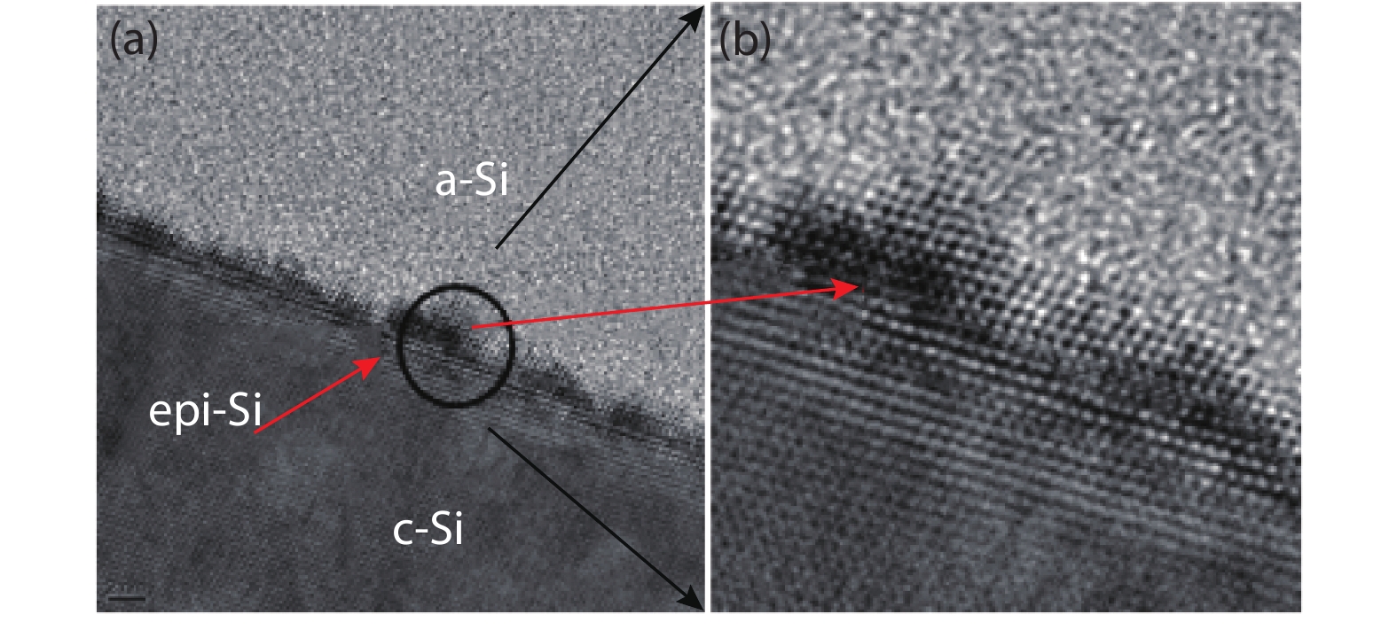
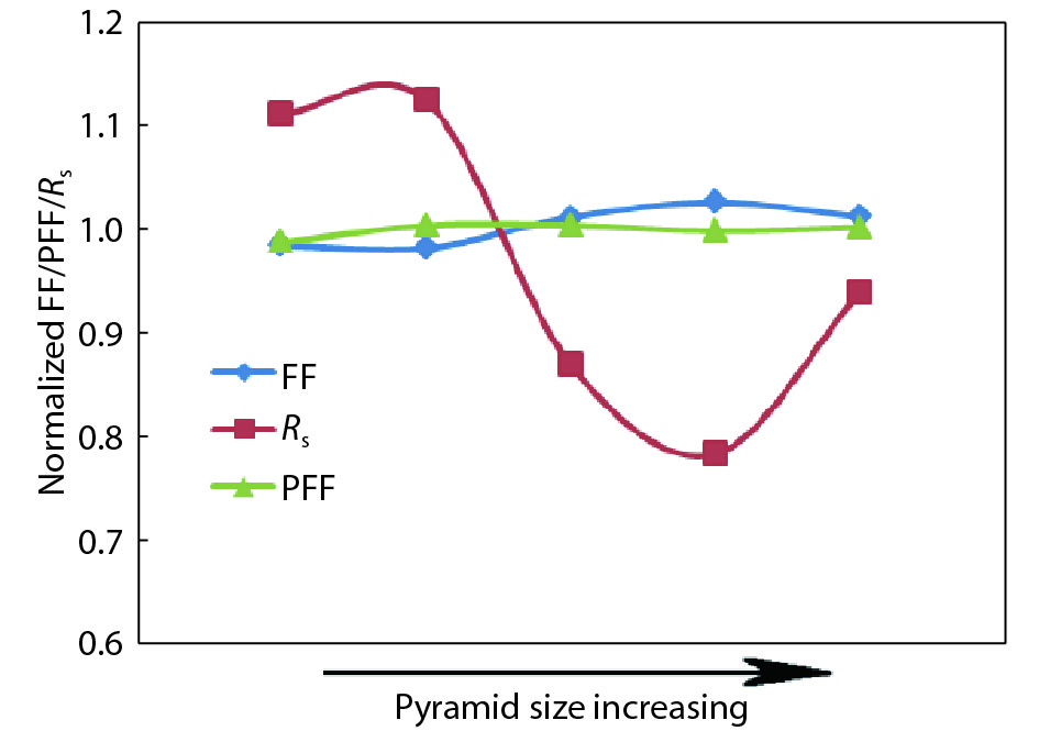
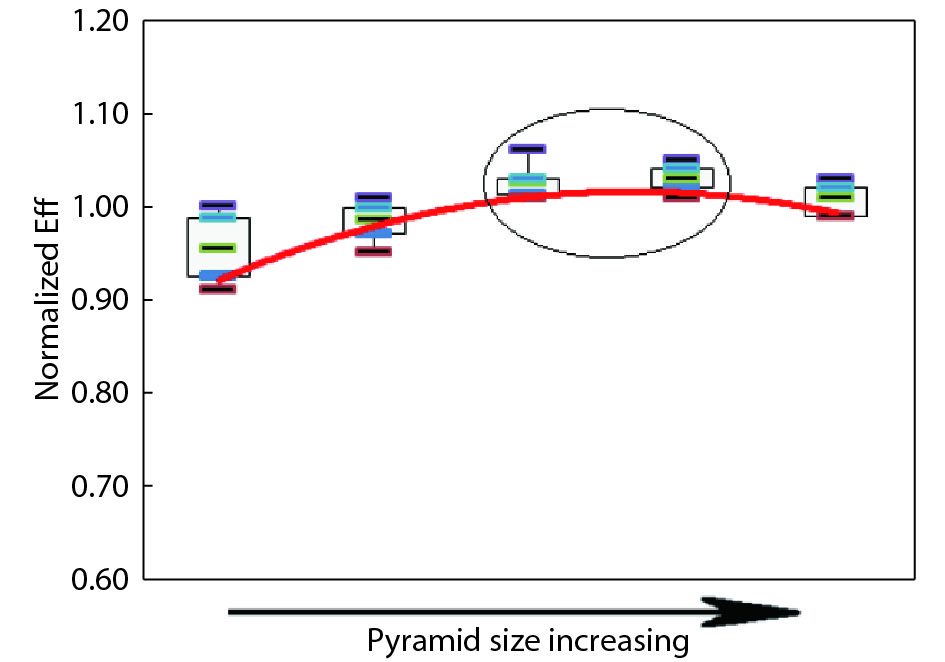
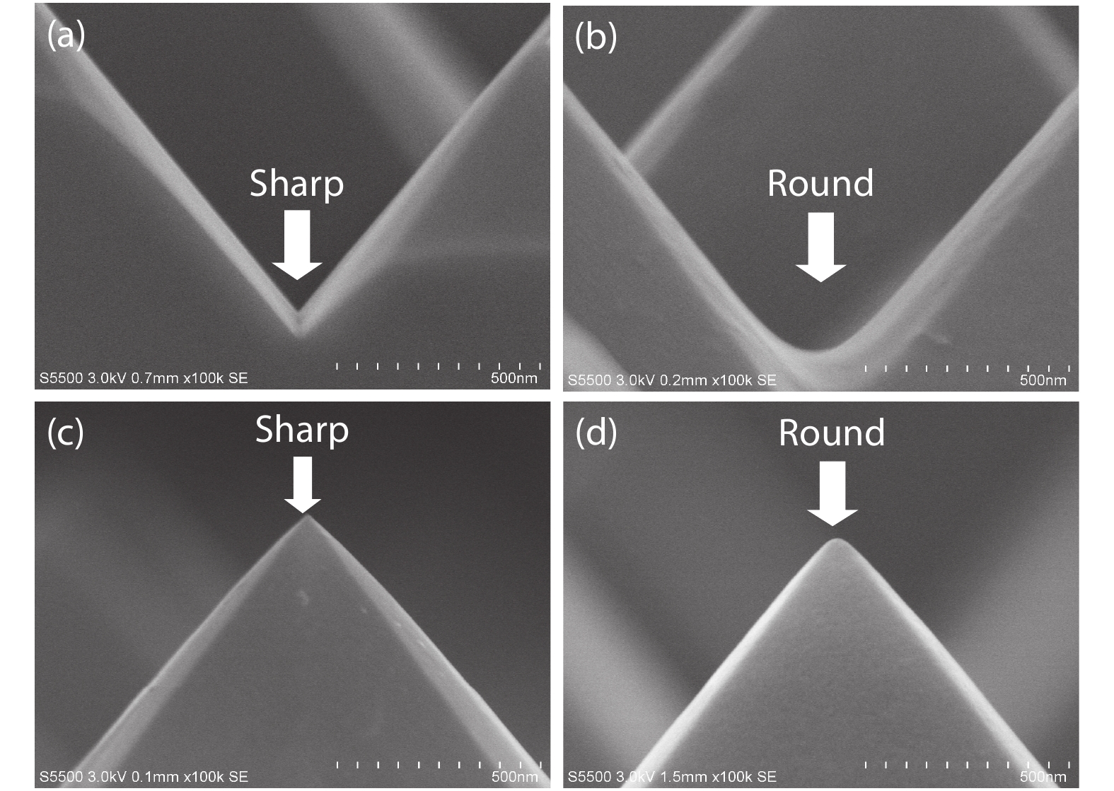
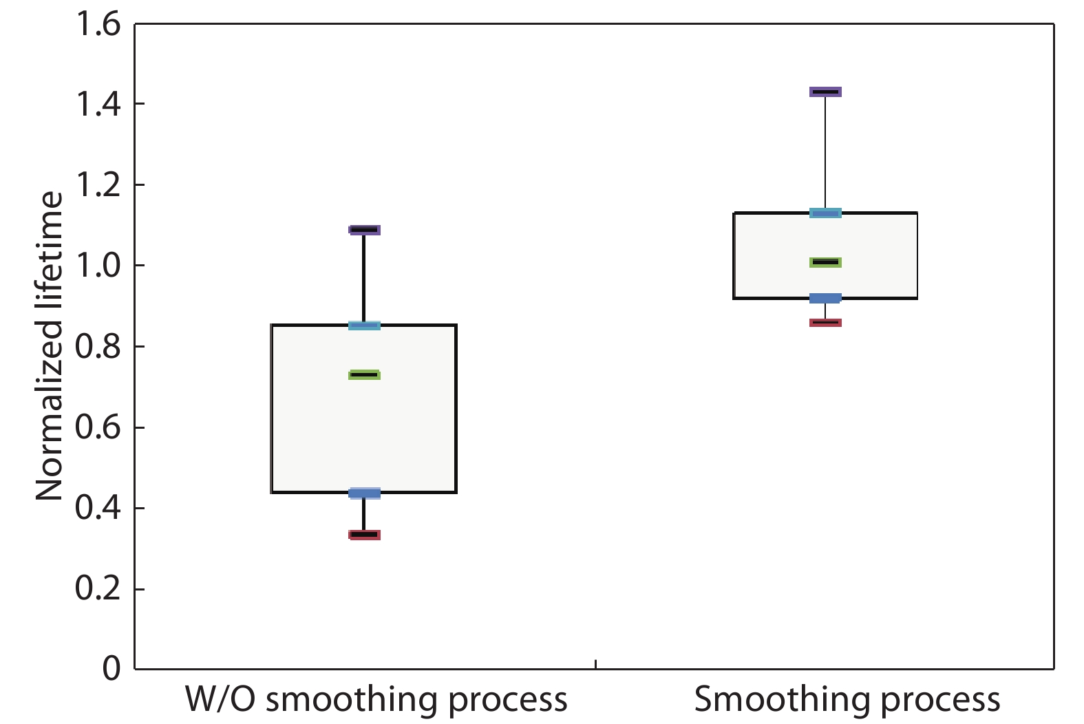
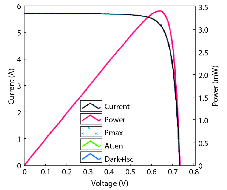
Pyramid size control and morphology treatment for high-efficiency silicon heterojunction solar cells
J. Semicond.
2019, 40(3): 032703 doi: 10.1088/1674-4926/40/3/032703

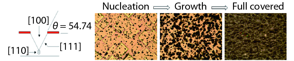
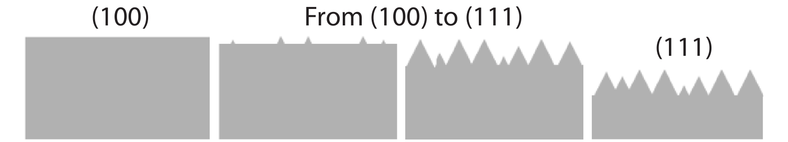
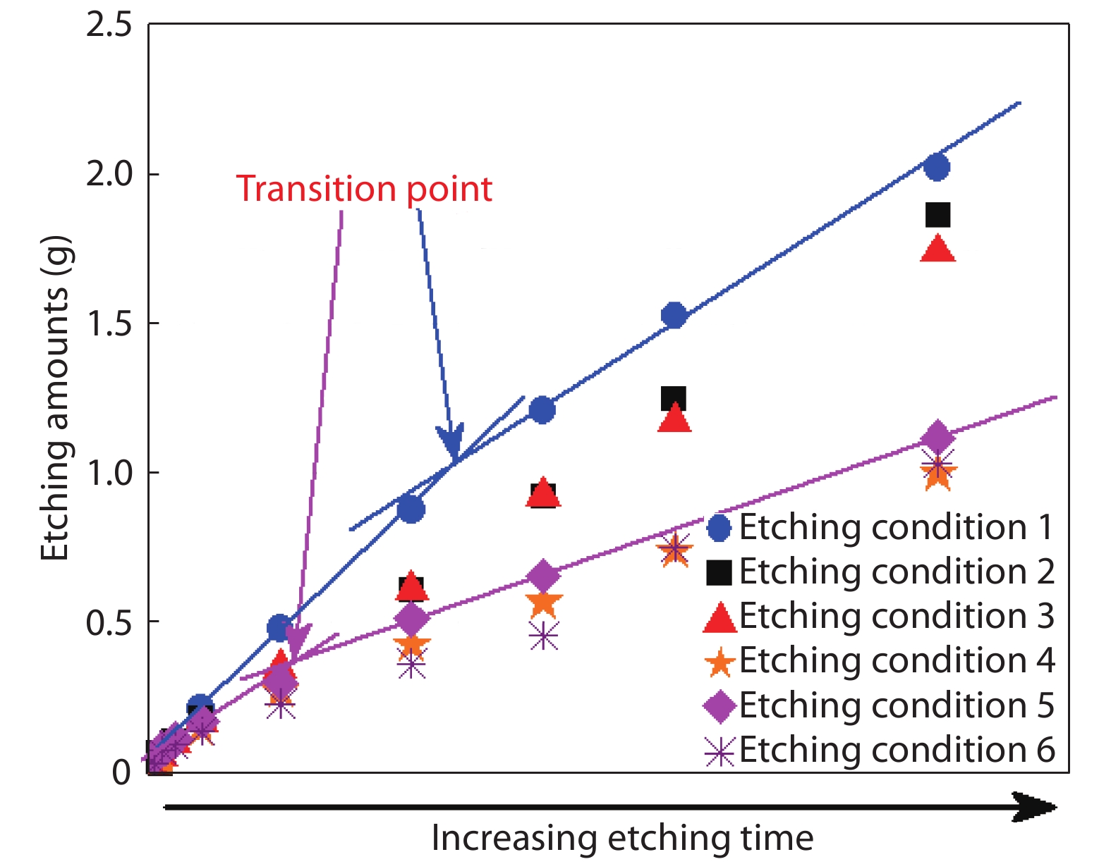
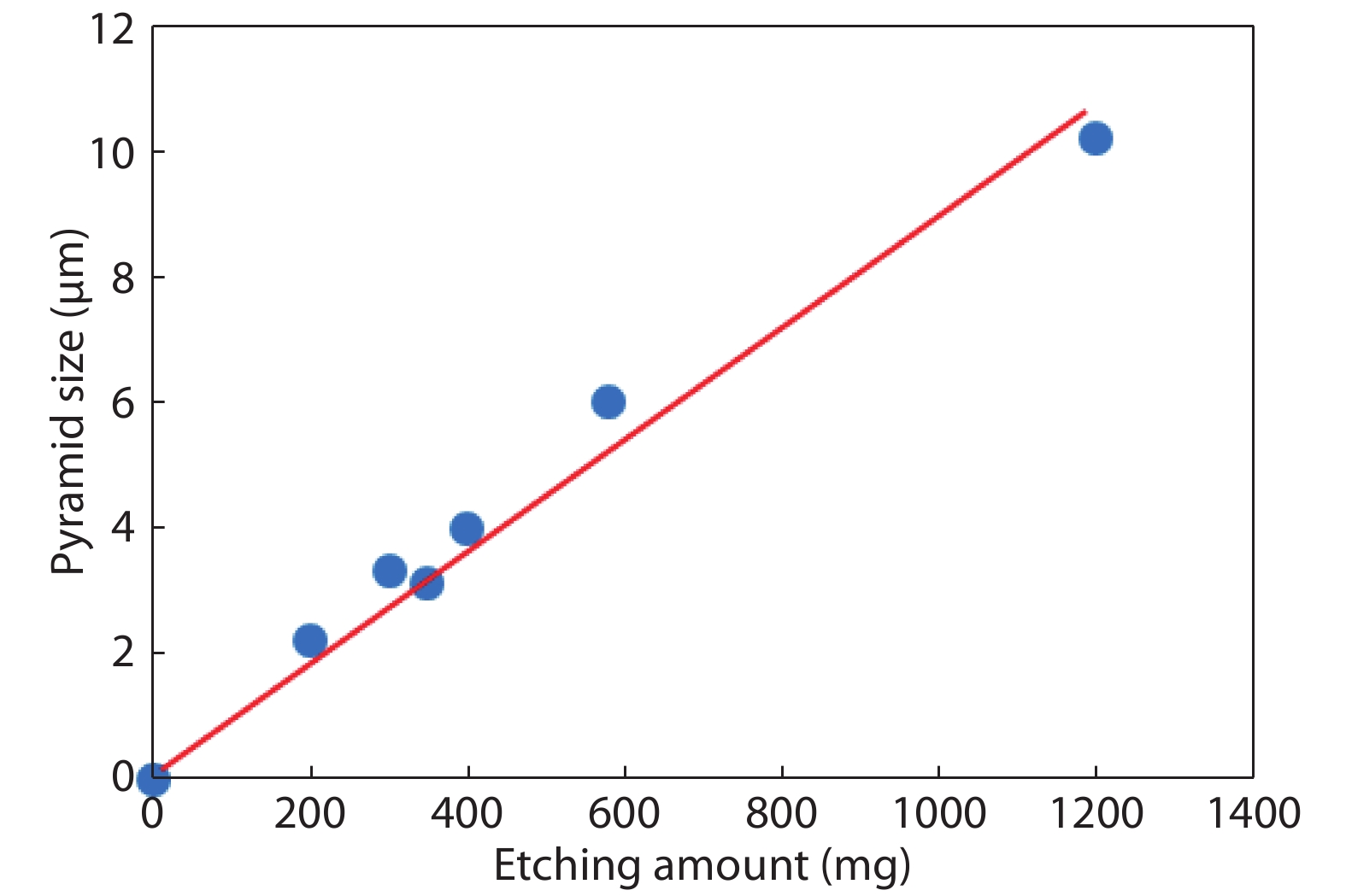
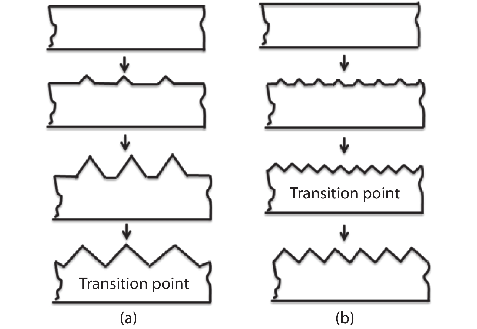
This paper investigates the formation process of surface pyramid and etching characteristics during the texturing process of mono-crystalline silicon wafers. It is found that there is an etch rate transition point in alkaline anisotropic etching when {100} plane-dominated etch turns to {111} plane-dominated etch, and the pyramid size has a strong linear correlation with the etch amount at the transition point. Several techniques were developed to control the pyramid size by monitoring and adjusting the etching amount. A wide range of average pyramid sizes were successfully achieved, from 0.5 to 12 μm. The experiments of the pyramid size on the light reflectance, the minority carrier lifetime (MCLT), and the performance of silicon heterojunction (SHJ) solar cells were carried out and analyzed. A desirable range of pyramid sizes was empirically determined by our investigation. In order to reduce the density states on the texturing surface, the wet-chemical smoothing treatment was also investigated. The smoothing treatment improves the passivation quality and the performance of the solar cells. Through pyramid size control and morphology treatment, together with the amorphous silicon (a-Si:H) deposition improvement, and electrode optimization, high performance of SHJ solar cells has been achieved, up to conversion efficiency 23.6%.


J. Semicond.
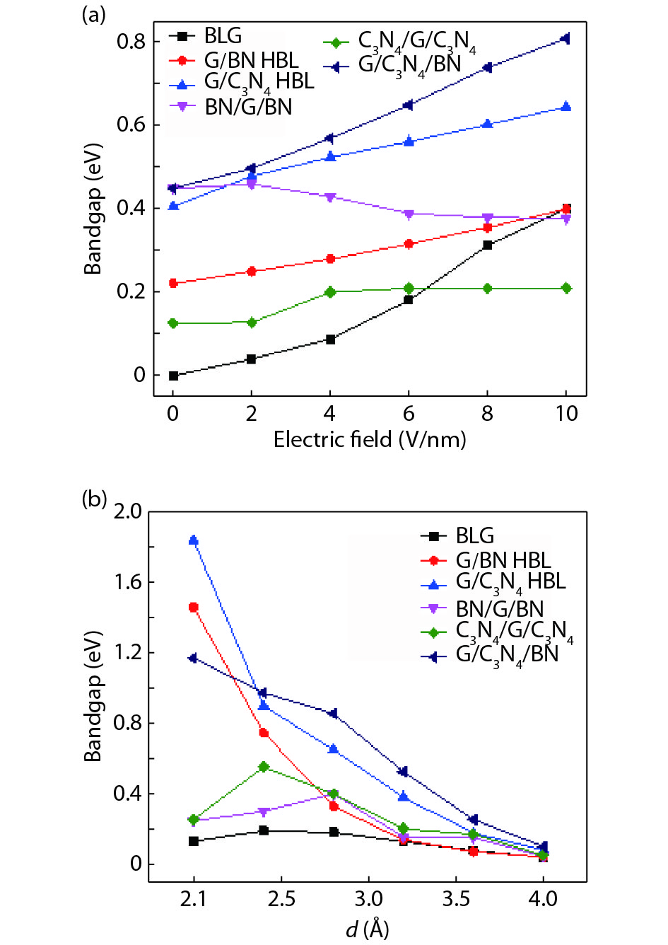
2019, 40(3): 032801 doi: 10.1088/1674-4926/40/3/032801
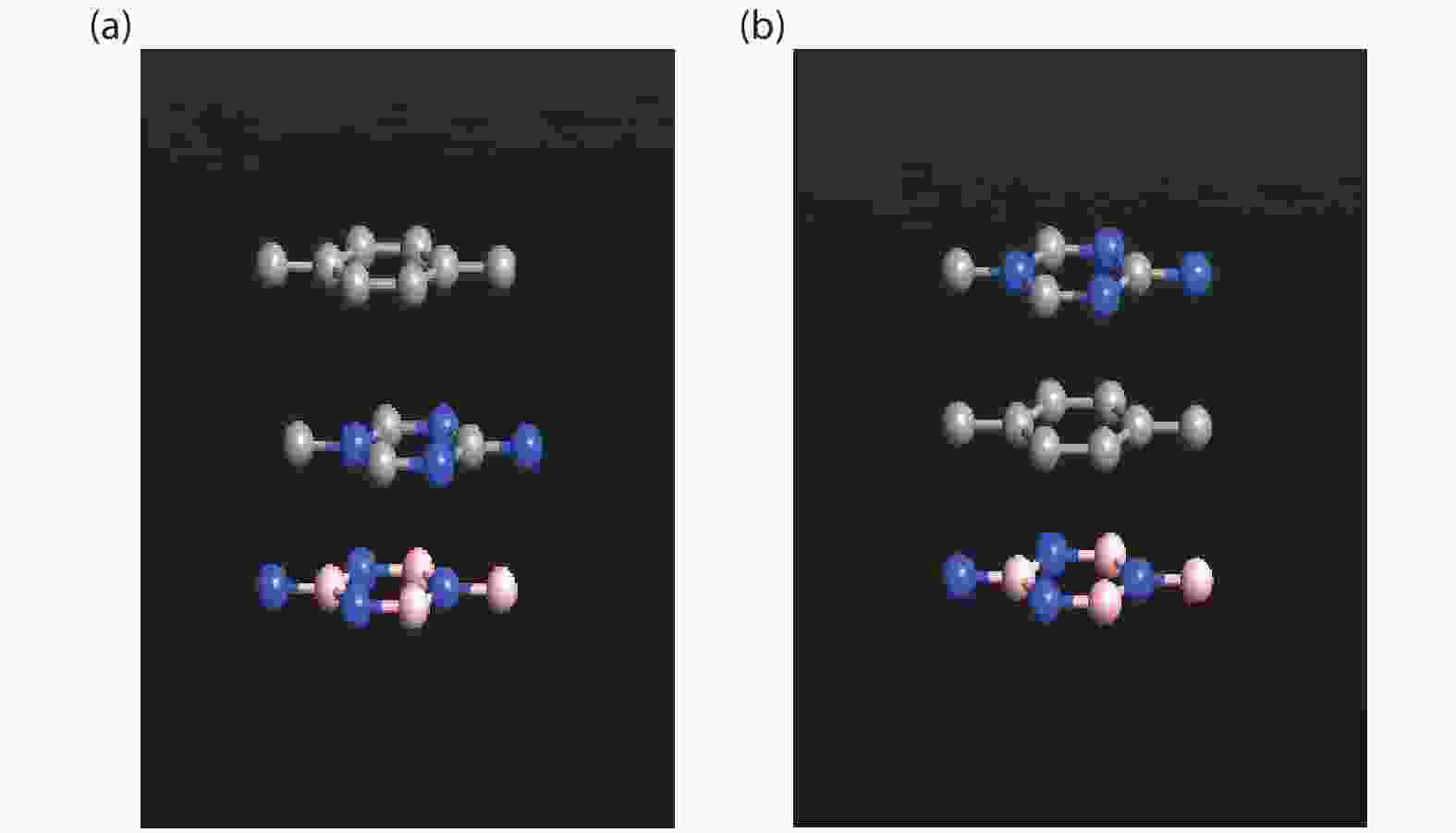
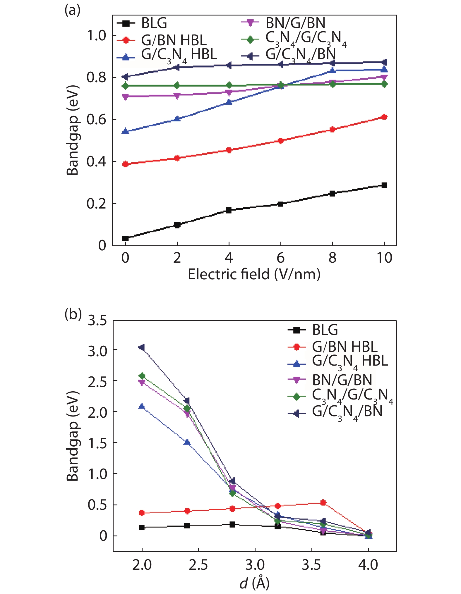
The effect of an external electric field on the bandgap is observed for two proposed heterostructures graphitic carbon nitride-graphene-hexagonal boron nitride (g-C3N4/G/h-BN) in hexagonal stack (AAA) and graphene-graphitic carbon nitride-hexagonal boron nitride (G/g-C3N4/h-BN) in Bernal stack (ABA). Their inter-layer distance, binding energy and effective mass has also been calculated. The structure optimization has been done by density functional theory (DFT) with van der Waals corrections. The inter-layer distance, bandgap, binding energy and effective mass has been listed for these heterostructures and compared with that of bilayer graphene (BLG), graphene-hexagonal boron nitride (G/h-BN) hetero-bilayer, graphene-graphitic carbon nitride (G/g-C3N4) hetero-bilayer and graphitic carbon nitride-graphene- graphitic carbon nitride (g-C3N4/G/g-C3N4) heterostructure in Bernal and hexagonal stack. g-C3N4/G/h-BN is found to offer lower effective mass and larger bandgap opening among the considered heterostructures.


J. Semicond.
2019, 40(3): 032802 doi: 10.1088/1674-4926/40/3/032802
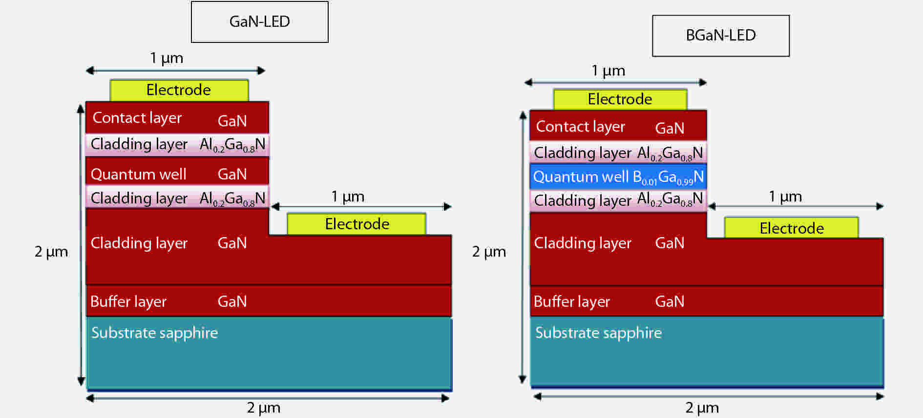
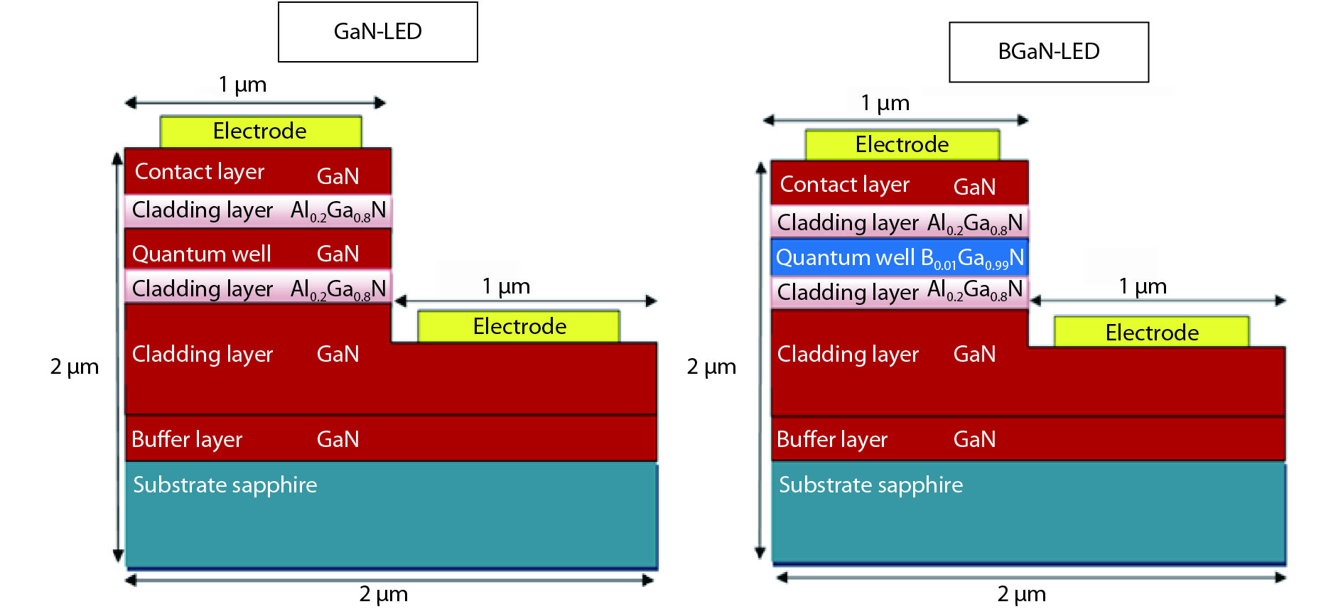
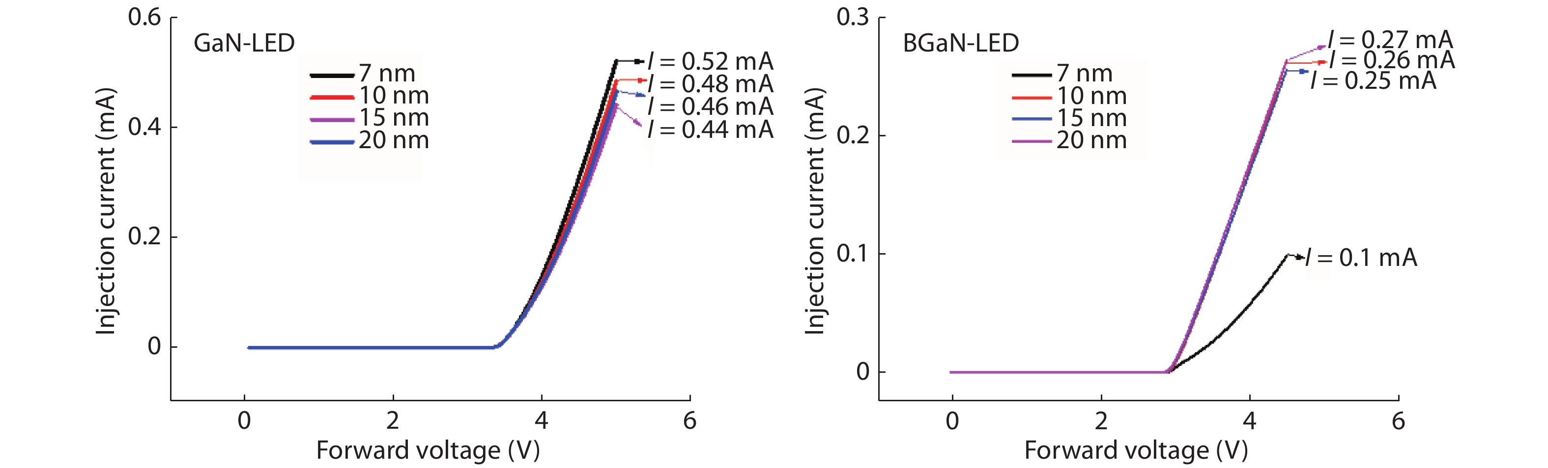
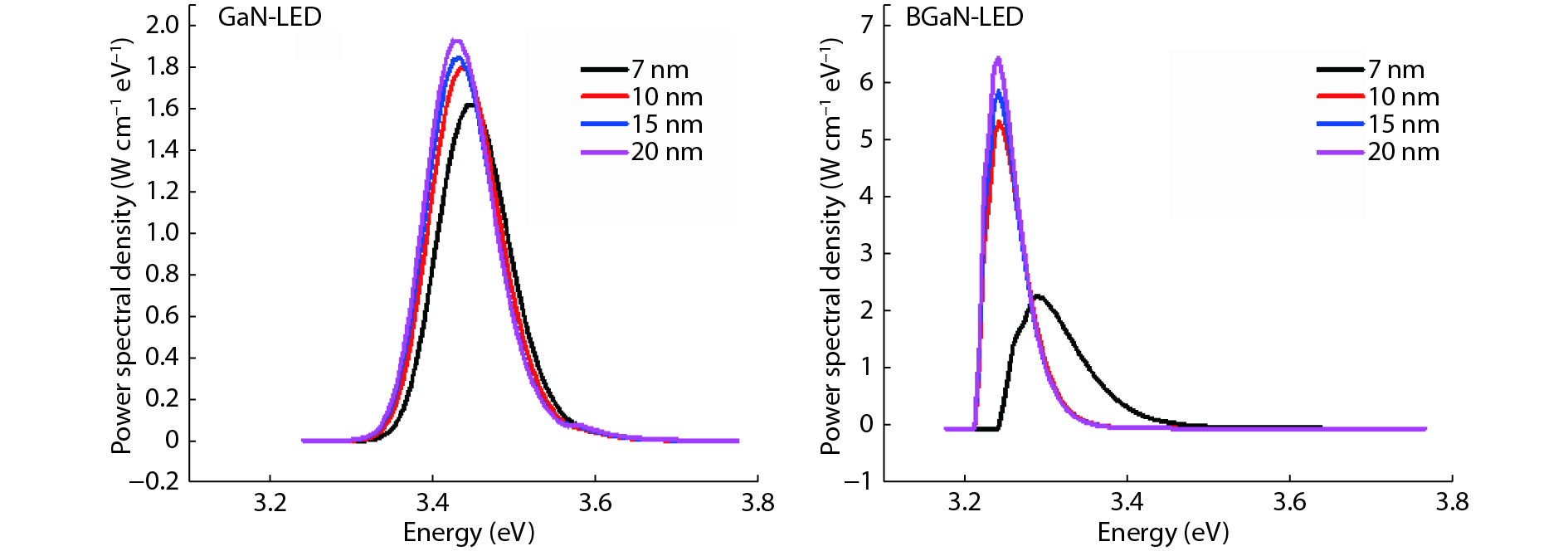
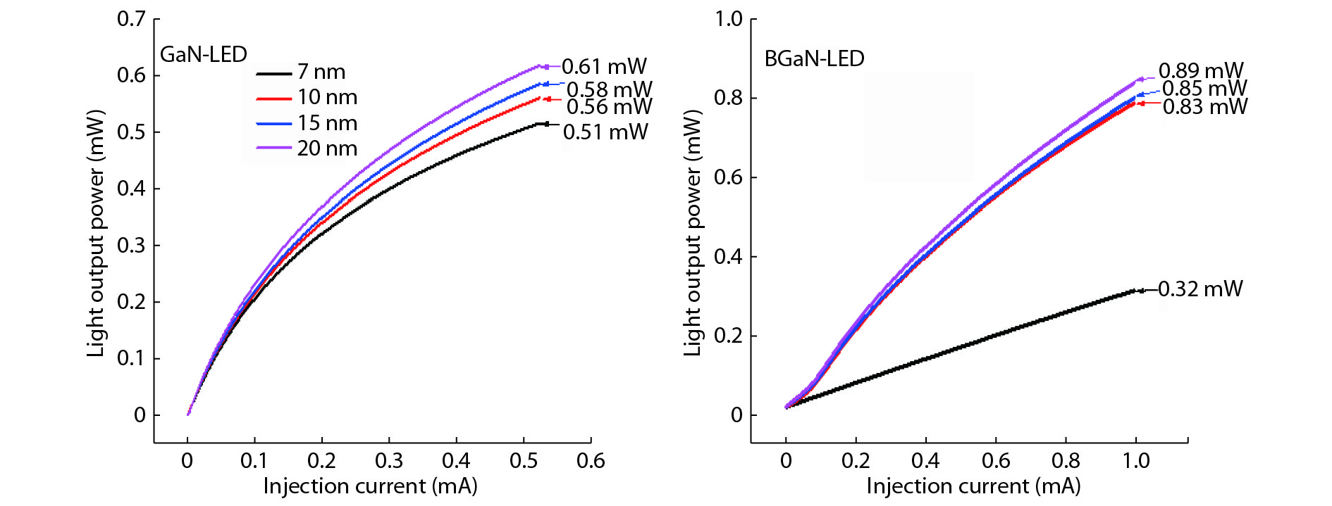
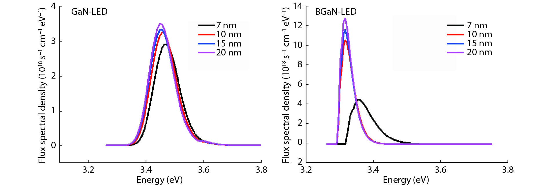
The objective of this work is to simulate a single quantum well ultraviolet light emitting diode (LED) based on AlGaN/GaN/AlGaN and AlGaN/BGaN/AlGaN, by using TCAD Silvaco simulator. The first structure has a GaN quantum well taken between two layers, of n-AlGaN and p-AlGaN. The second one has a BGaN quantum well instead of GaN. We fix the concentration of the boron in BGaN to only 1% and we vary the thickness of GaN and BGaN quantum well layer from 7 to 20 nm, for the two structures. As results, we obtain respectively for GaN-LED and BGaN-LED, a maximum current of 0.52 and 0.27 mA, a maximum power spectral density of 1.935 and 6.7 W cm−1 eV−1, a maximum spontaneous emission of 3.34 × 1028 and 3.43 × 1028 s−1 cm−3 eV−1, and a maximum Light output power of 0.56 and 0.89 mW.