Issue Browser
Volume 40, Issue 6,
Jun 2019
J. Semicond.
2019, 40(6): 061001 doi: 10.1088/1674-4926/40/6/061001
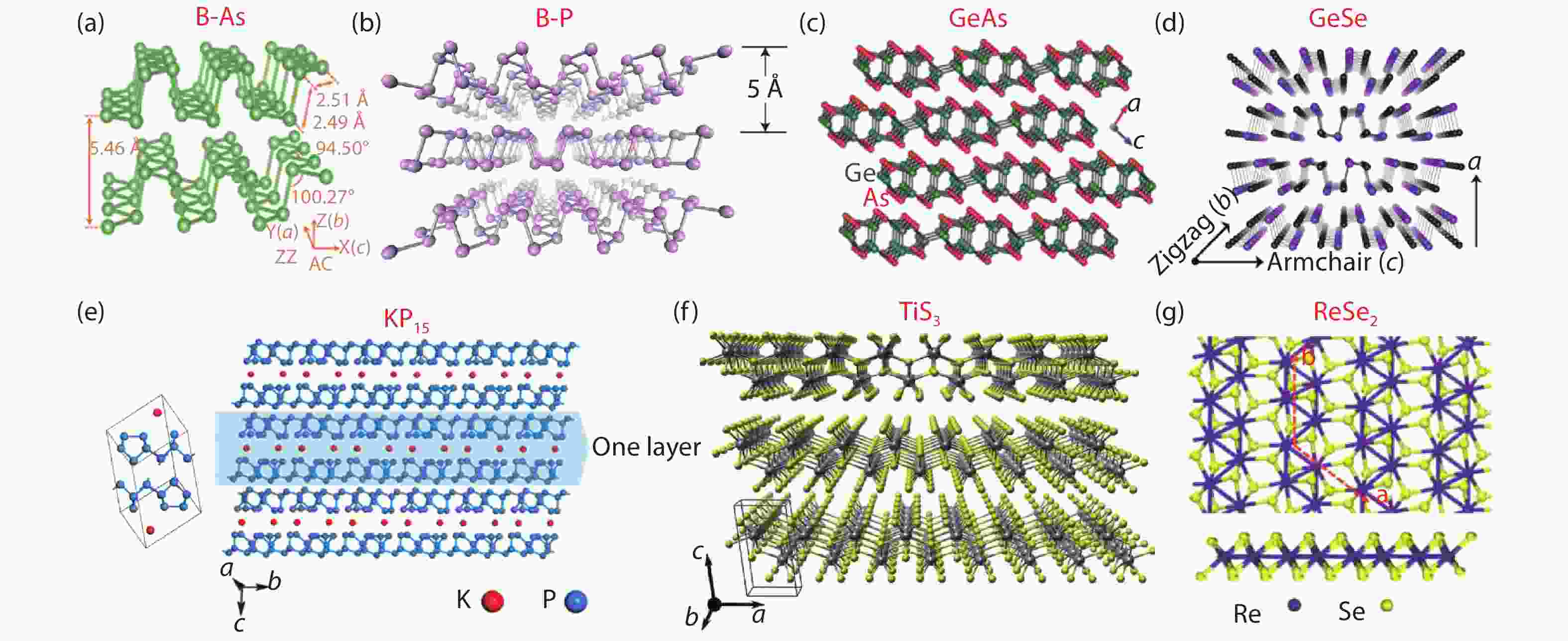
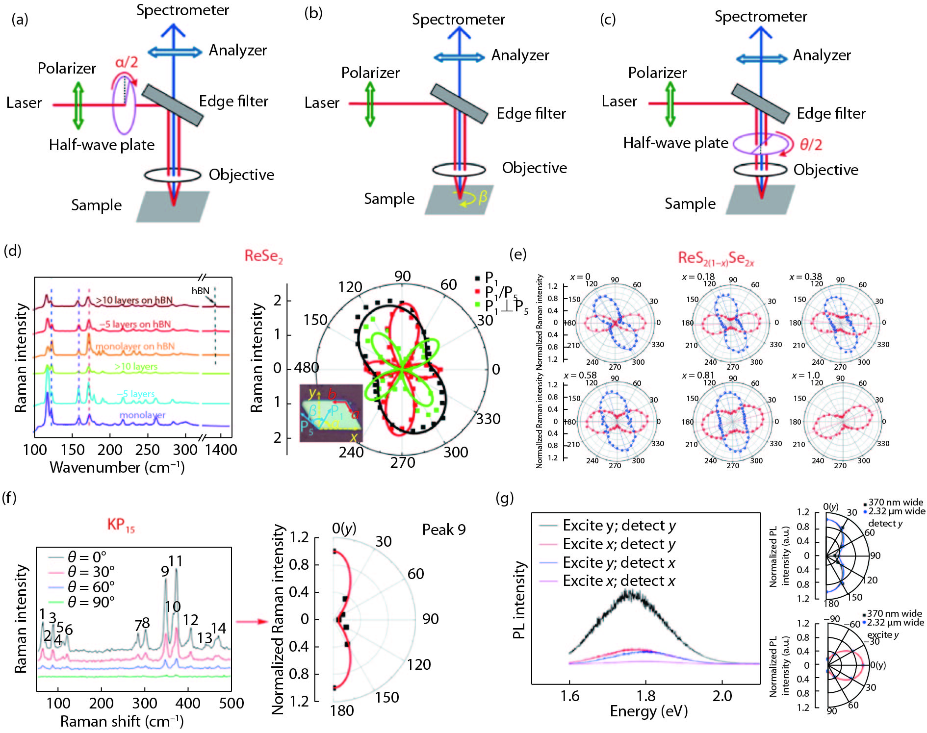
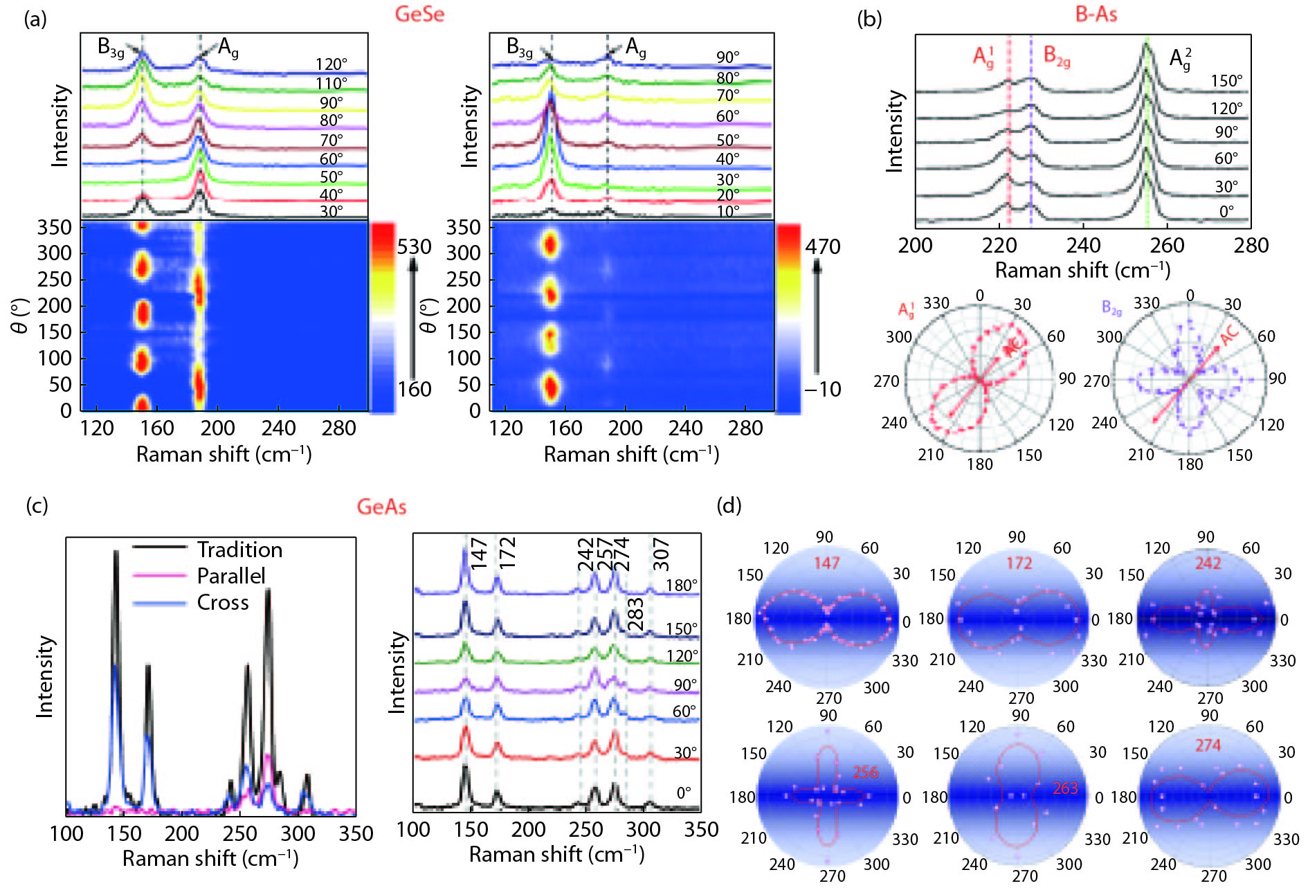
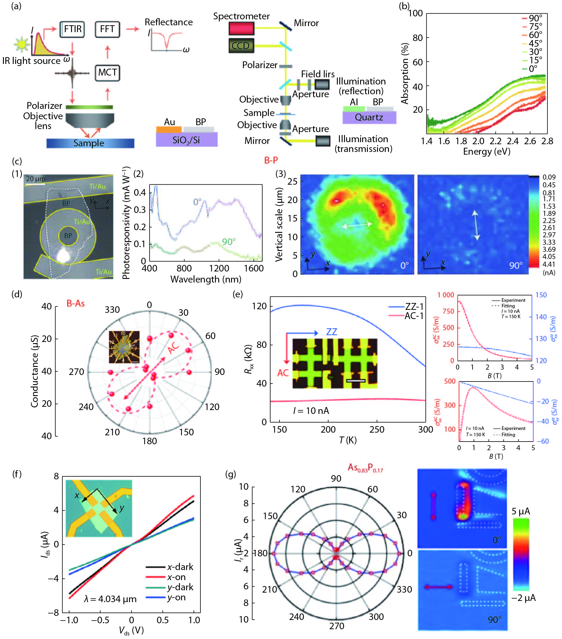
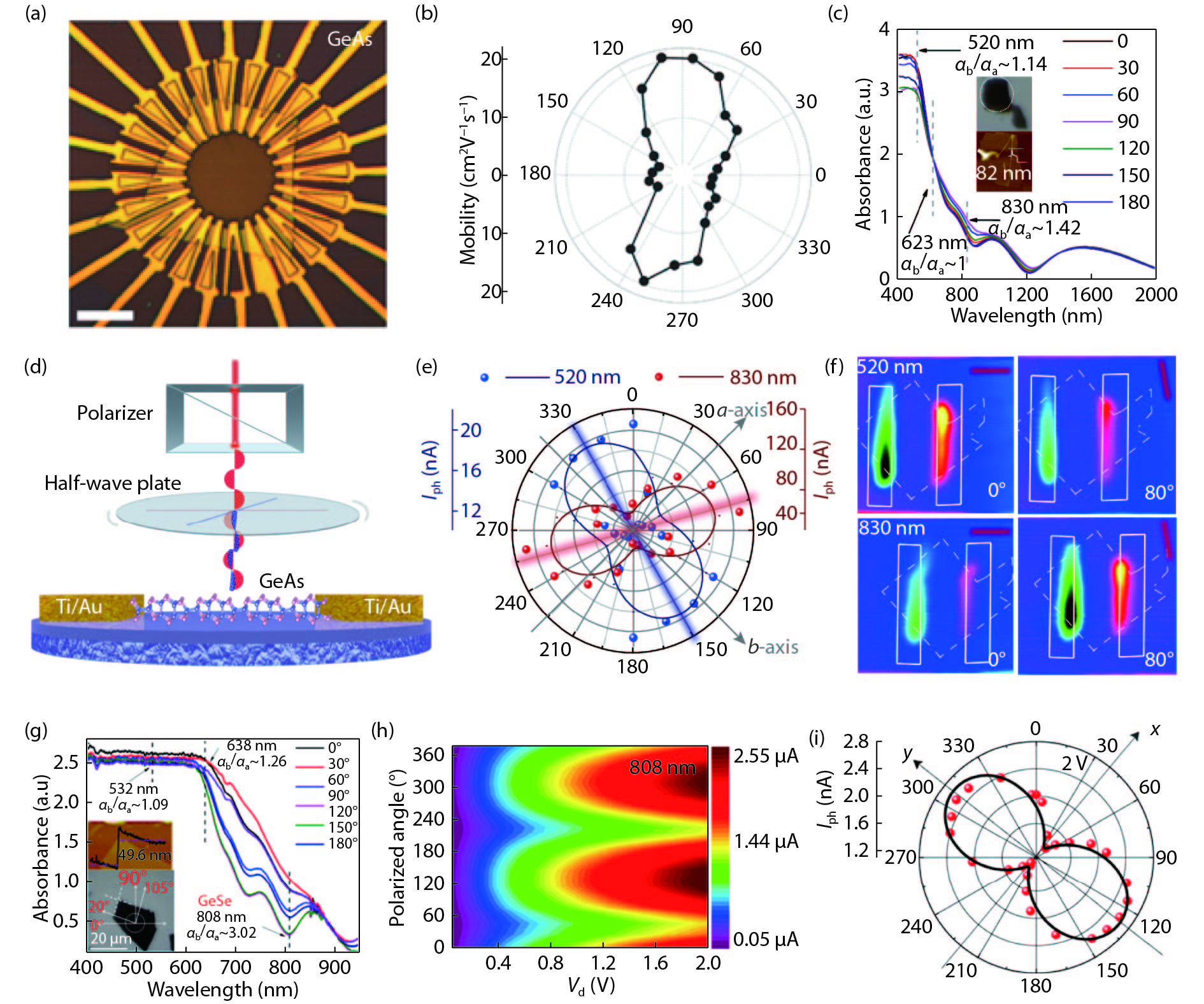
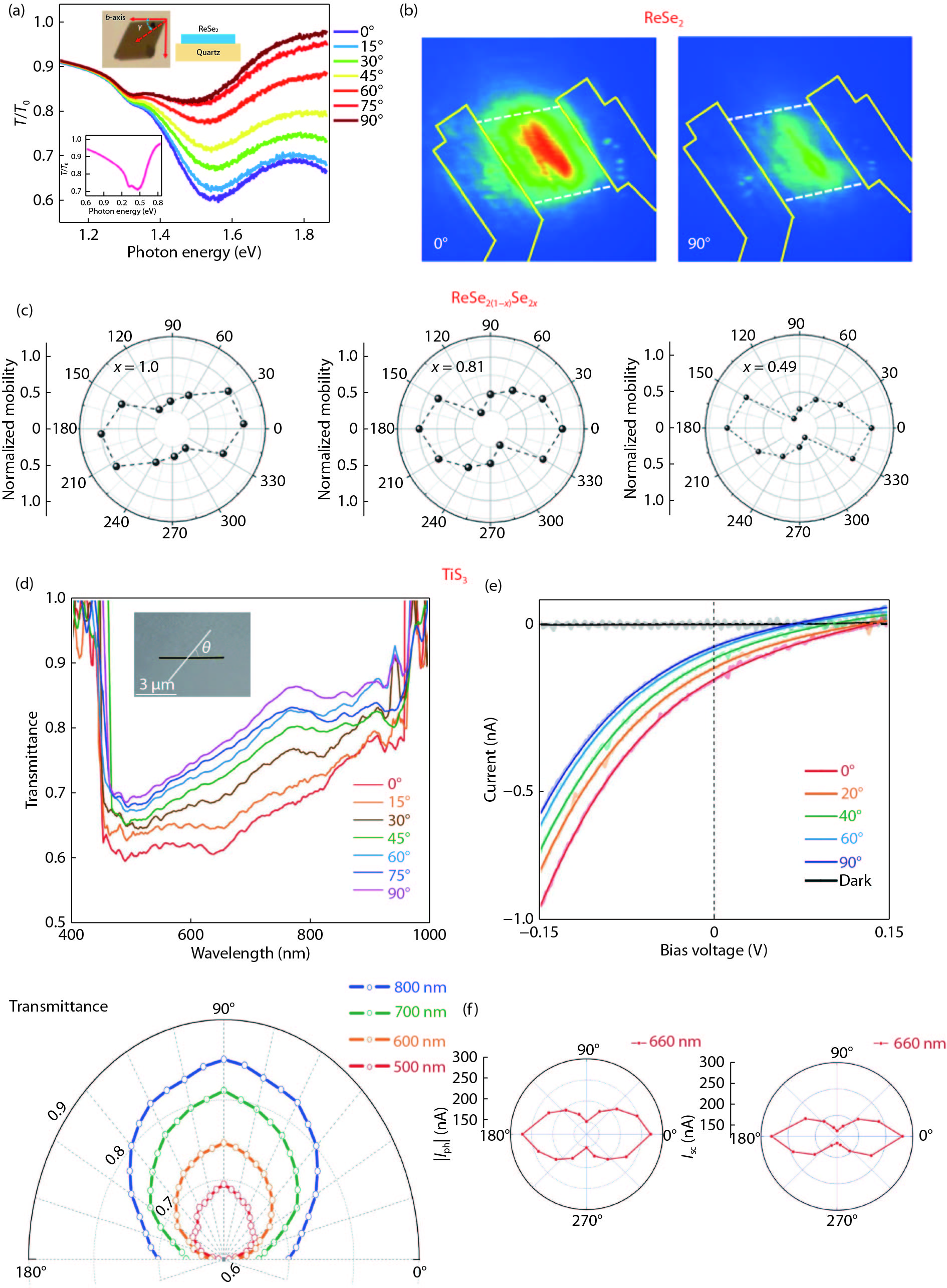
Two-dimensional (2D) anisotropic materials, such as B-P, B-As, GeSe, GeAs, ReSe2, KP15 and their hybrid systems, exhibit unique crystal structures and extraordinary anisotropy. This review presents a comprehensive comparison of various 2D anisotropic crystals as well as relevant FETs and photodetectors, especially on their particular anisotropy in optical and electrical properties. First, the structure of typical 2D anisotropic crystal as well as the analysis of structural anisotropy is provided. Then, recent researches on anisotropic Raman spectra are reviewed. Particularly, a brief measurement principle of Raman spectra under three typical polarized measurement configurations is introduced. Finally, recent progress on the electrical and photoelectrical properties of FETs and polarization-sensitive photodetectors based on 2D anisotropic materials is summarized for the comparison between different 2D anisotropic materials. Beyond the high response speed, sensitivity and on/off ratio, these 2D anisotropic crystals exhibit highly conduction ratio and dichroic ratio which can be applied in terms of polarization sensors, polarization spectroscopy imaging, optical radar and remote sensing.

J. Semicond.
2019, 40(6): 061002 doi: 10.1088/1674-4926/40/6/061002

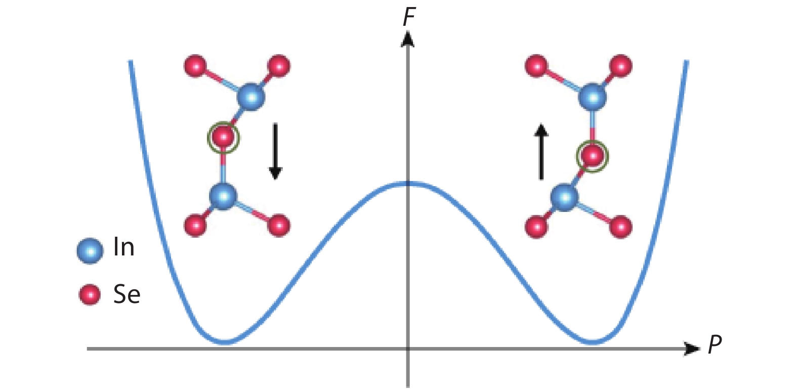
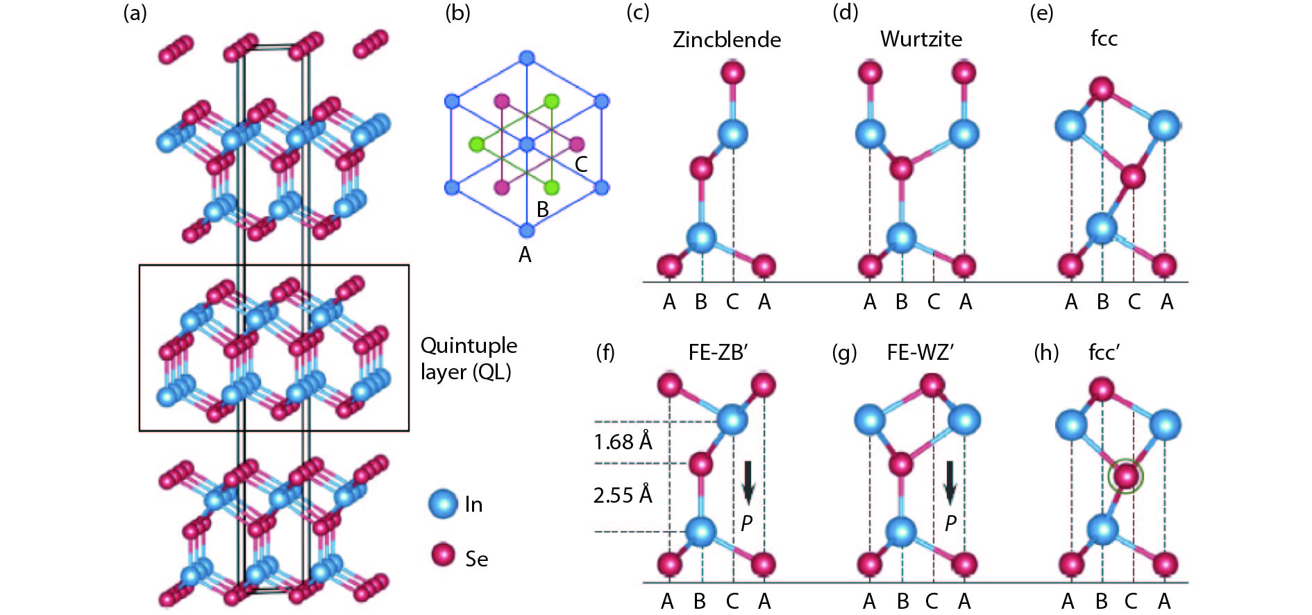
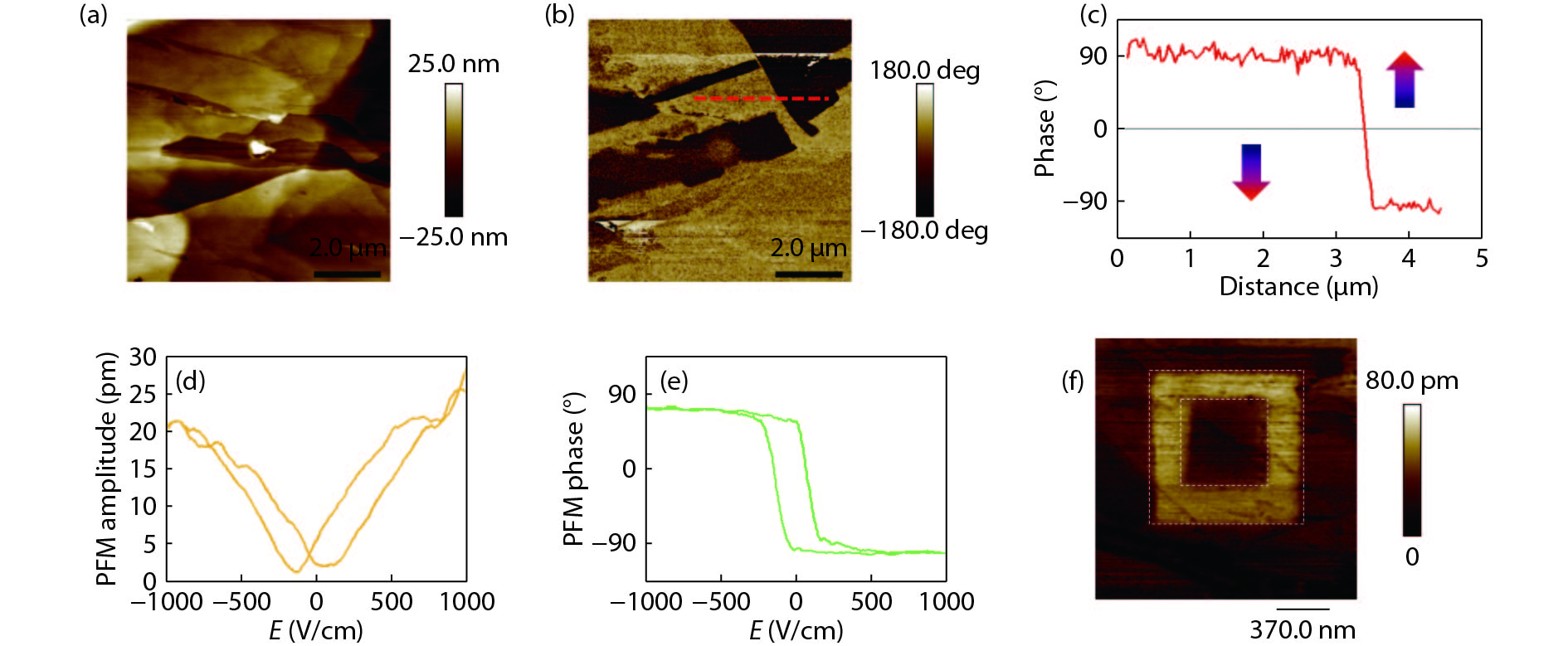
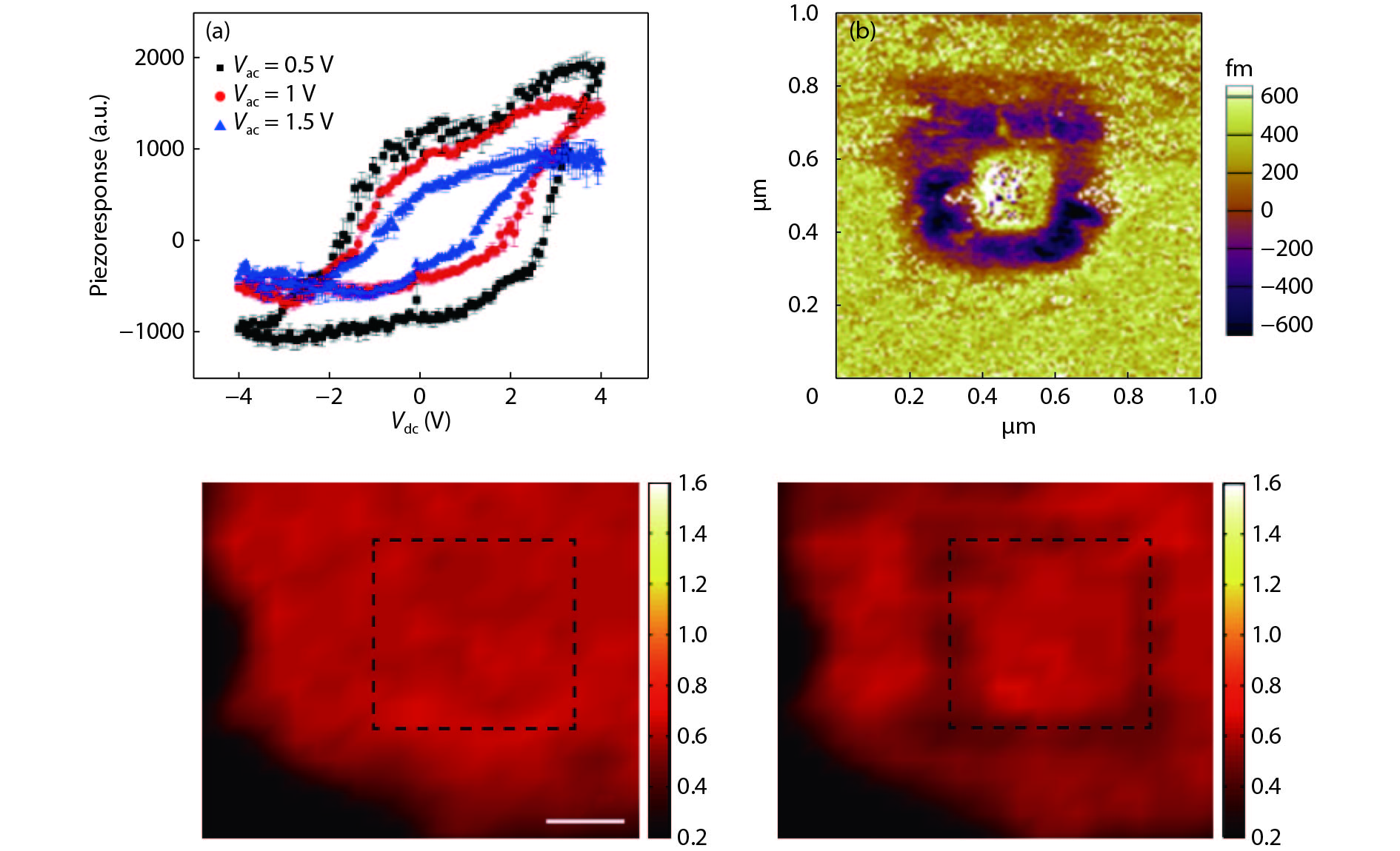
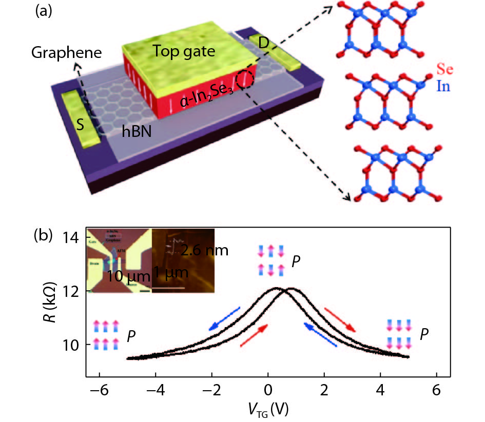
Room temperature ferroelectric thin films are the key element of high-density nonvolatile memories in modern electronics. However, with the further miniaturization of the electronic devices beyond the Moore’s law, conventional ferroelectrics suffer great challenge arising from the critical thickness effect, where the ferroelectricity is unstable if the film thickness is reduced to nanometer or single atomic layer limit. Two-dimensional (2D) materials, thanks to their stable layered structure, saturate interfacial chemistry, weak interlayer couplings, and the benefit of preparing stable ultra-thin film at 2D limit, are promising for exploring 2D ferroelectricity and related device applications. Therefore, it provides an effective approach to overcome the limitation in conventional ferroelectrics with the study of 2D ferroelectricity in van der Waals (vdW) materials. In this review article, we briefly introduce recent progresses on 2D ferroelectricity in layered vdW materials. We will highlight the study on atomically thin α-In2Se3, which is an emergent ferroelectric semiconductor with the coupled in-plane and out-of-plane ferroelectricity. Furthermore, two prototype ferroelectric devices based on ferroelectric α-In2Se3 will also be reviewed.

J. Semicond.
2019, 40(6): 061003 doi: 10.1088/1674-4926/40/6/061003

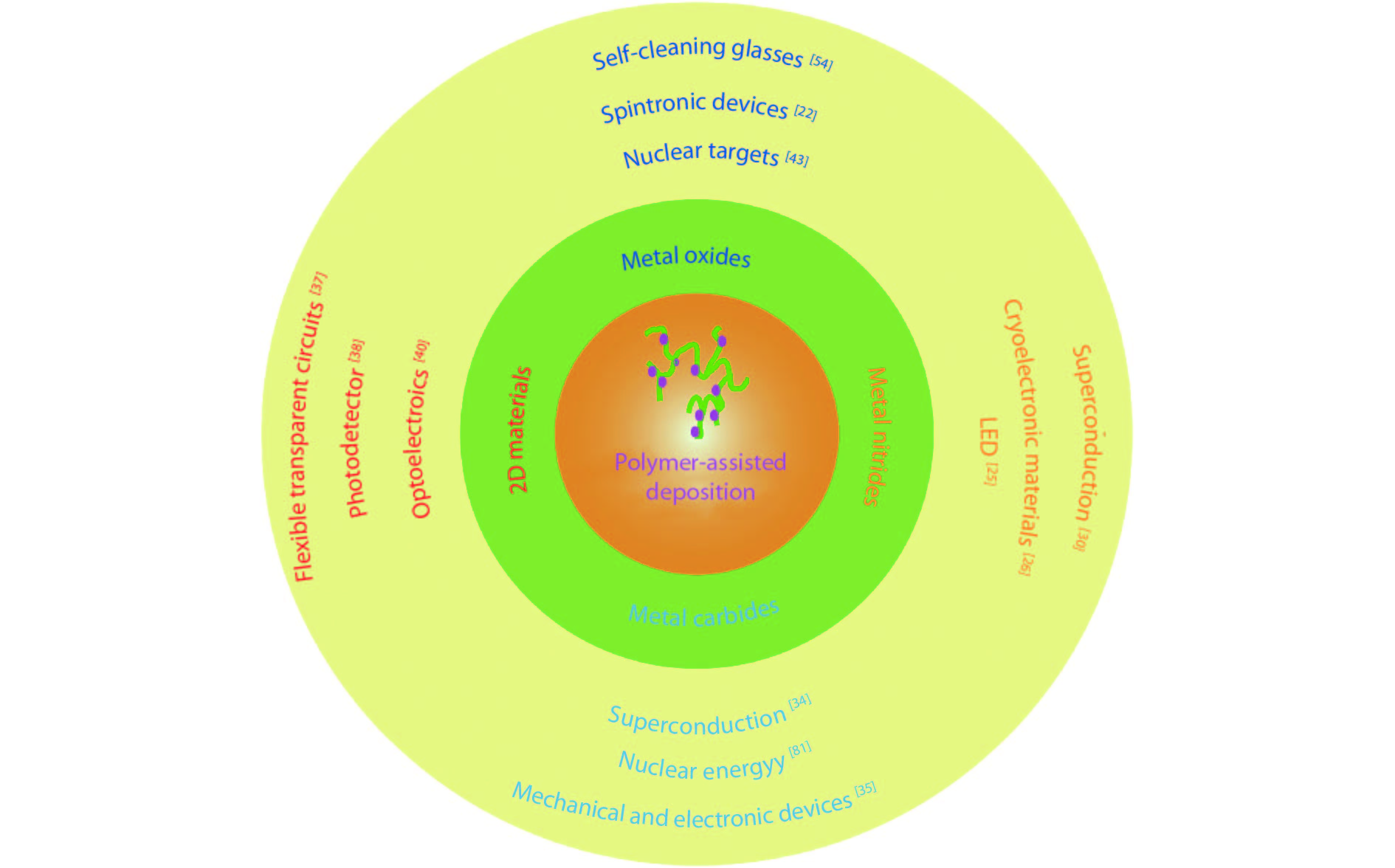
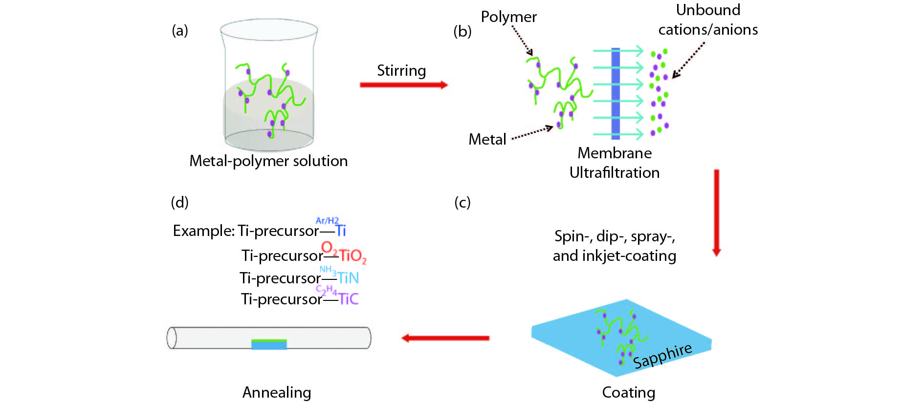
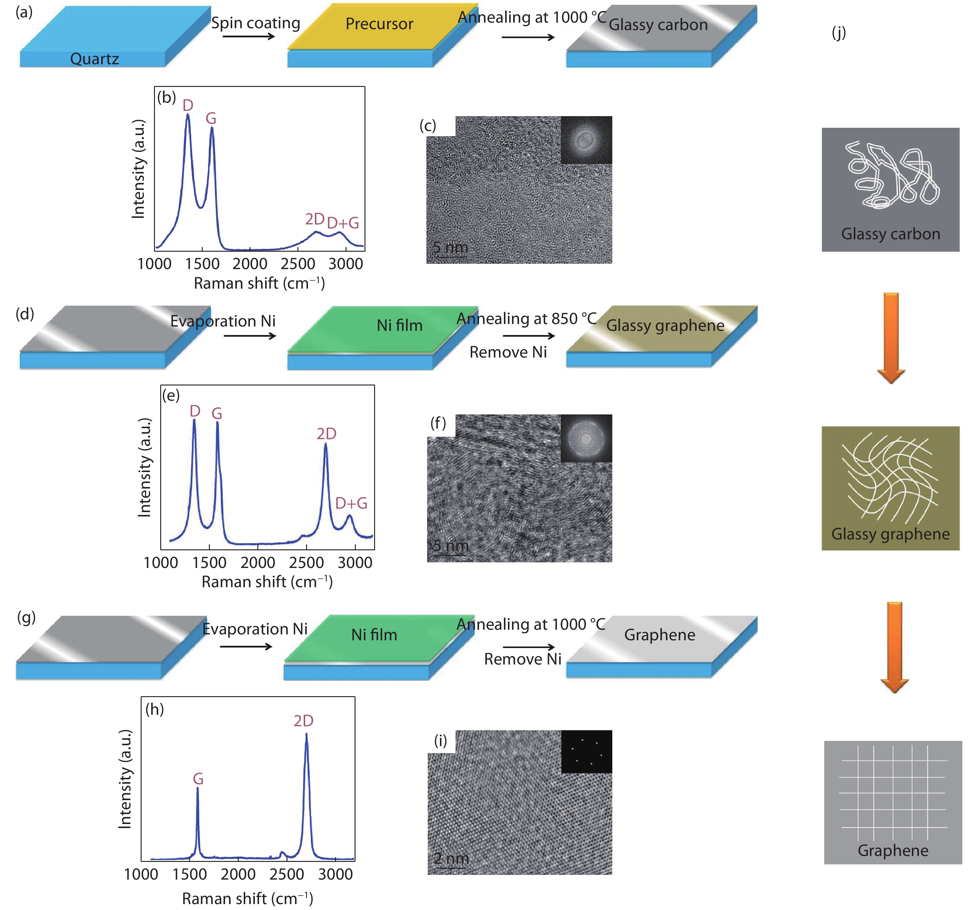
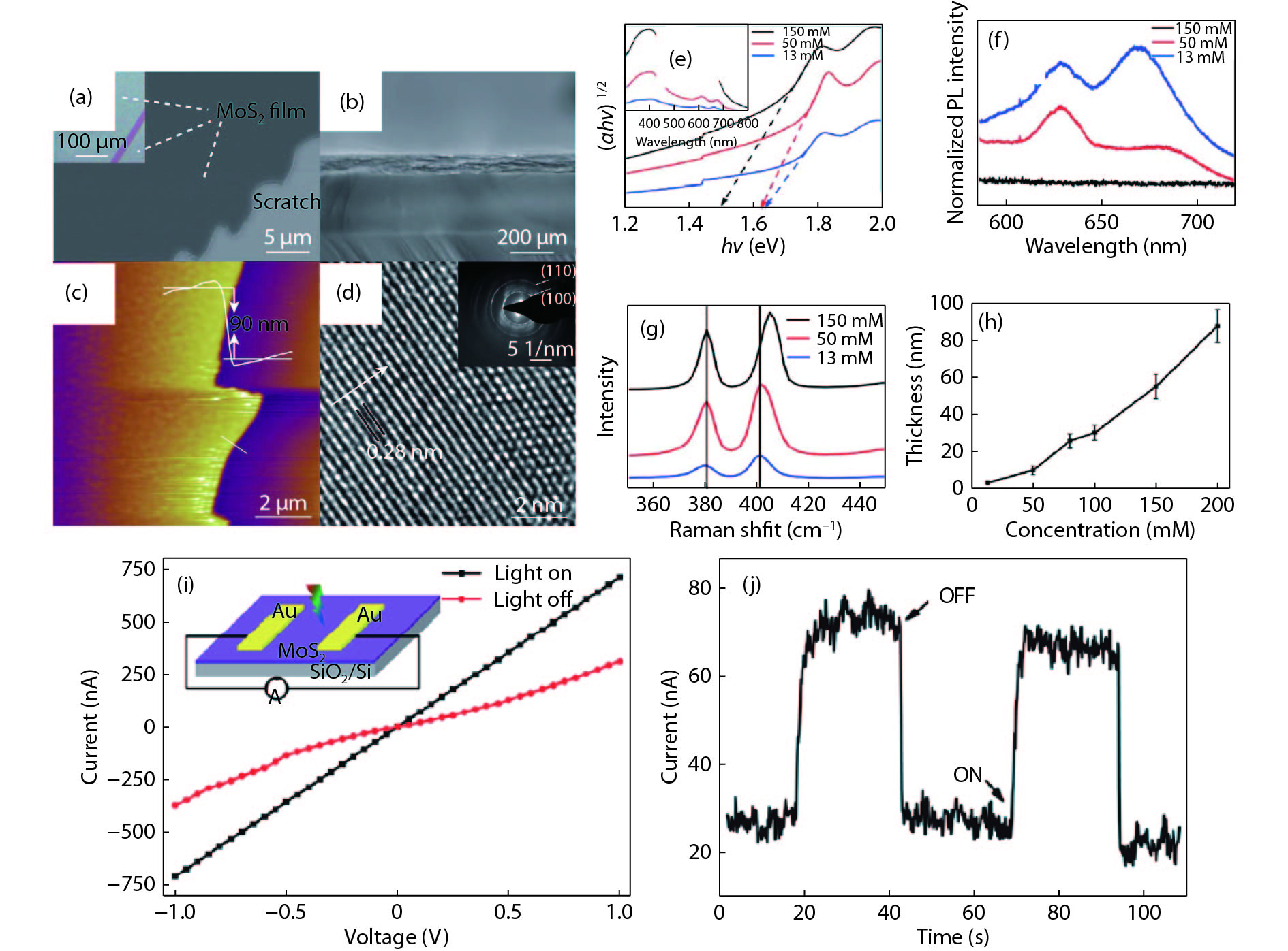
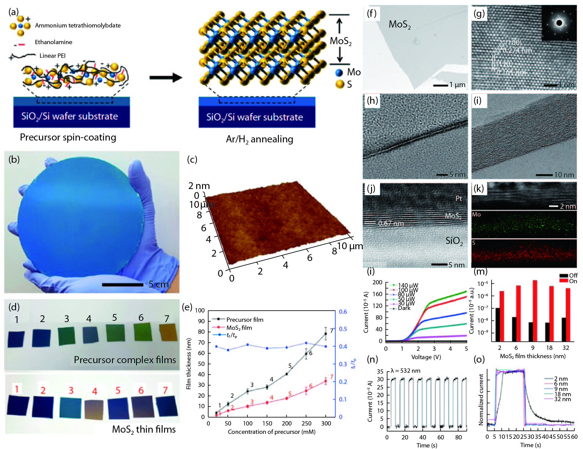
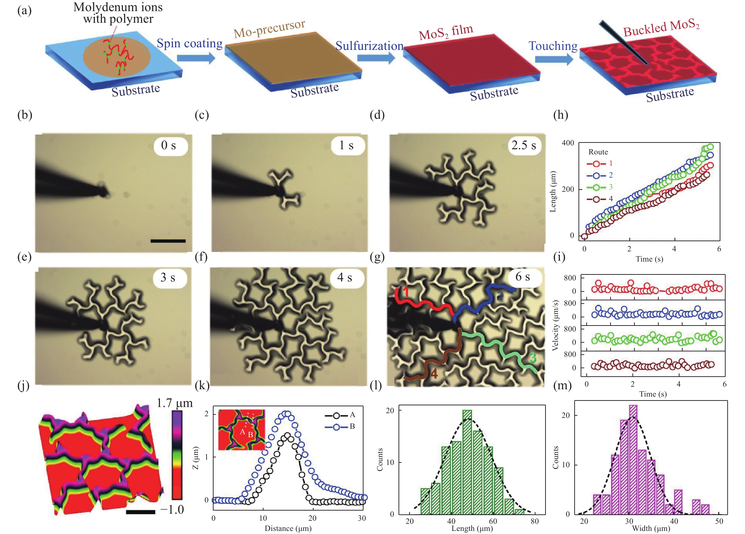
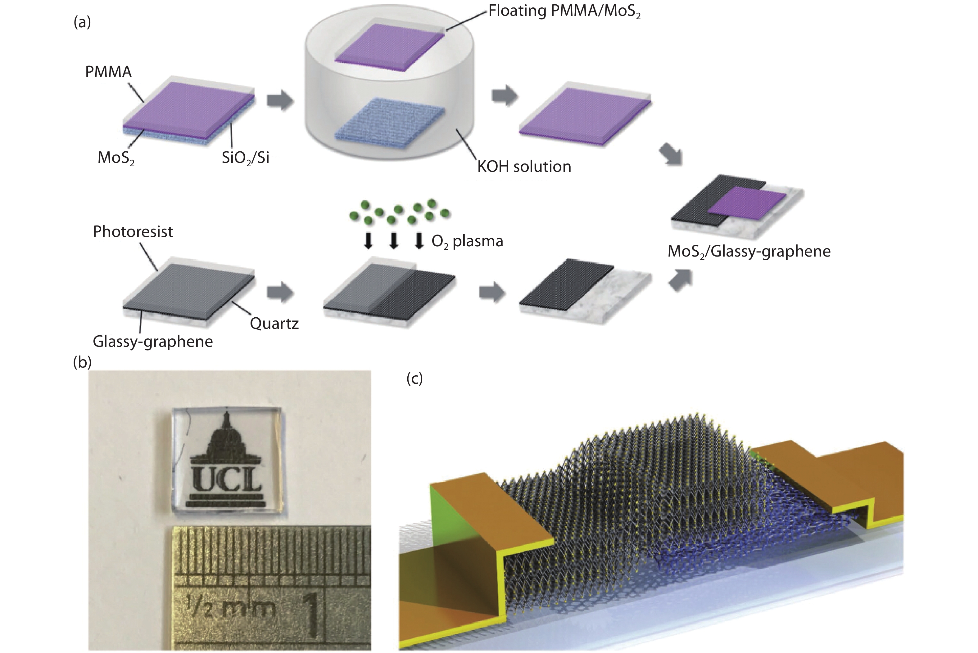
Two-dimensional (2D) materials have attracted considerable attention because of their novel and tunable electronic, optical, ferromagnetic, and chemical properties. Compared to mechanical exfoliation and chemical vapor deposition, polymer-assisted deposition (PAD) is more suitable for mass production of 2D materials owing to its good reproducibility and reliability. In this review, we summarize the recent development of PAD on syntheses of 2D materials. First, we introduce principles and processing steps of PAD. Second, 2D materials, including graphene, MoS2, and MoS2/glassy-graphene heterostructures, are presented to illustrate the power of PAD and provide readers with the opportunity to assess the method. Last, we discuss the future prospects and challenges in this research field. This review provides a novel technique for preparing 2D layered materials and may inspire new applications of 2D layered materials.


J. Semicond.
2019, 40(6): 062001 doi: 10.1088/1674-4926/40/6/062001

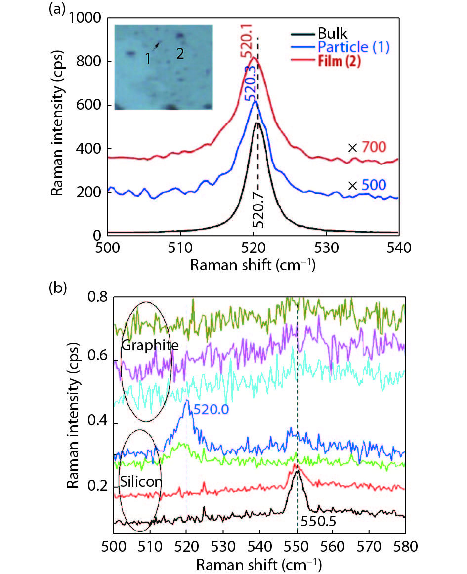
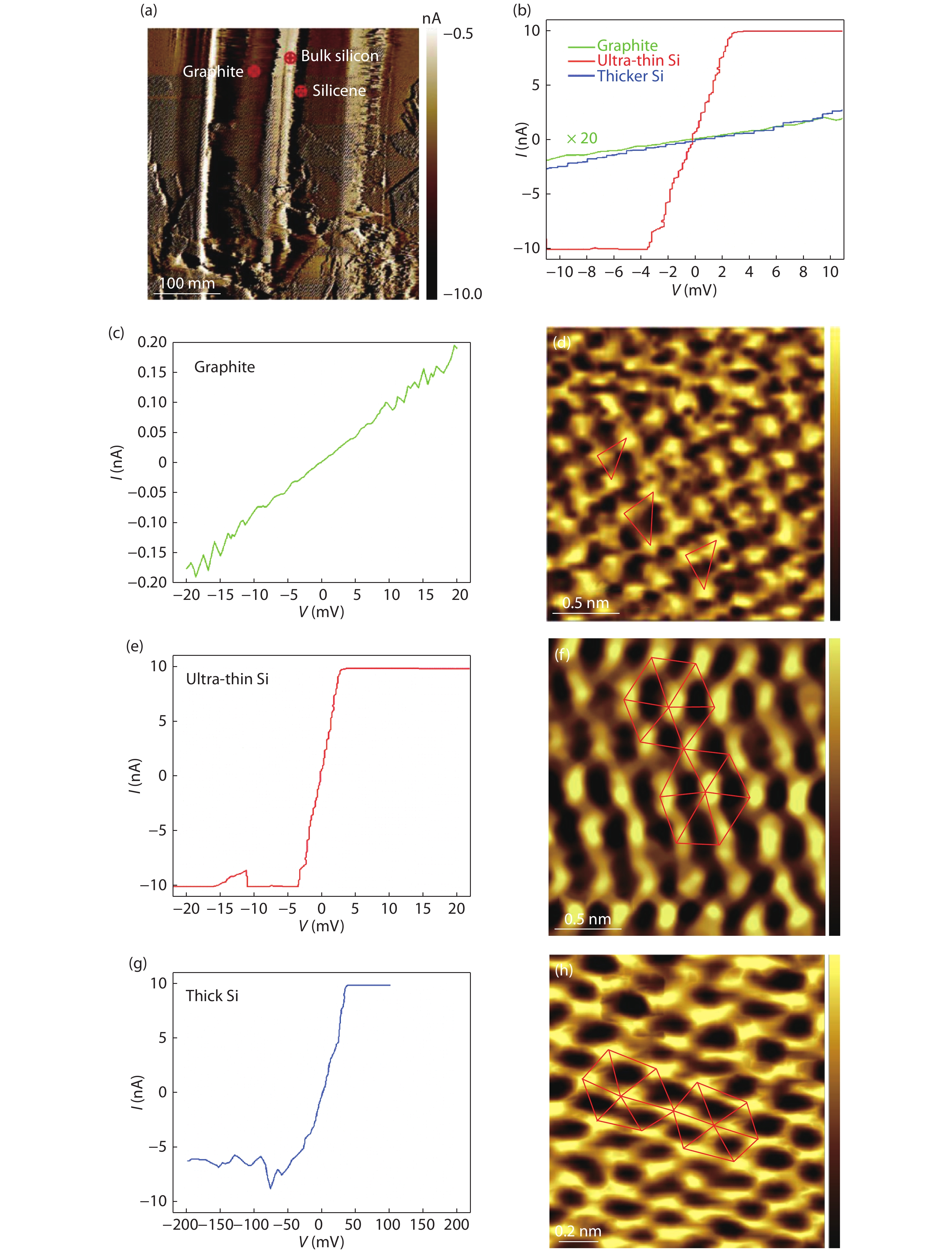
We report the growth of Si nanostructures, either as thin films or nanoparticles, on graphene substrates. The Si nanostructures are shown to be single crystalline, air stable and oxidation resistive, as indicated by the observation of a single crystalline Si Raman mode at around 520 cm–1, a STM image of an ordered surface structure under ambient condition, and a Schottky junction with graphite. Ultra-thin silicon regions exhibit silicene-like behavior, including a Raman mode at around 550 cm–1, a triangular lattice structure in STM that has distinctly different lattice spacing from that of either graphene or thicker Si, and metallic conductivity of up to 500 times higher than that of graphite. This work suggests a bottom-up approach to forming a Si nanostructure array on a large-scale patterned graphene substrate that can be used to fabricate nanoscale Si electronic devices.
J. Semicond.
2019, 40(6): 062002 doi: 10.1088/1674-4926/40/6/062002
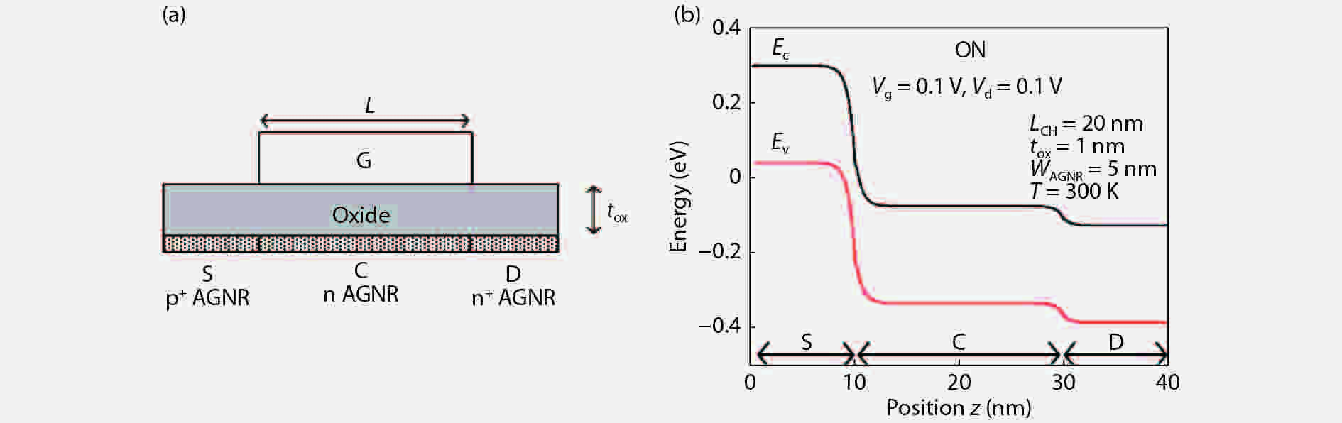
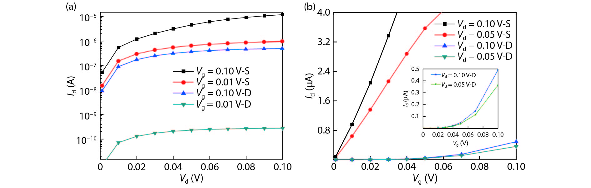
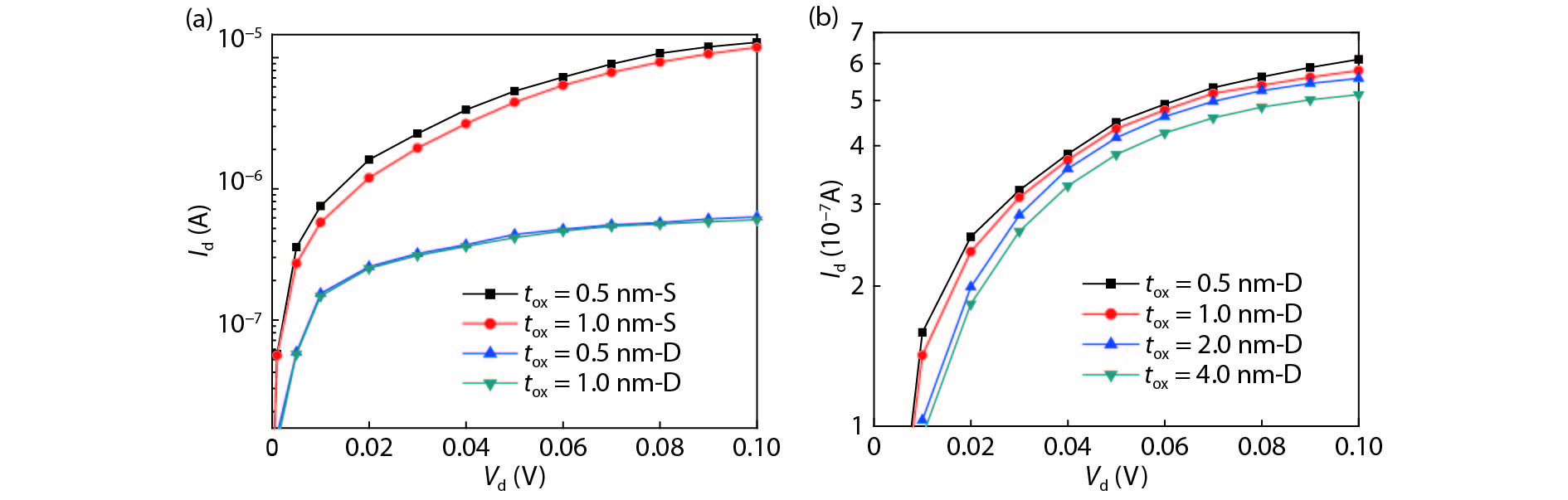
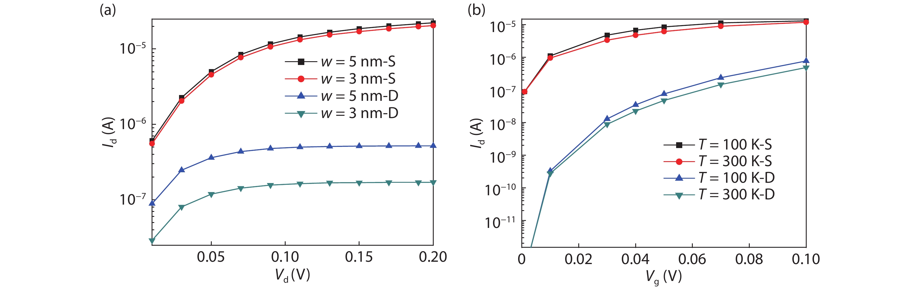
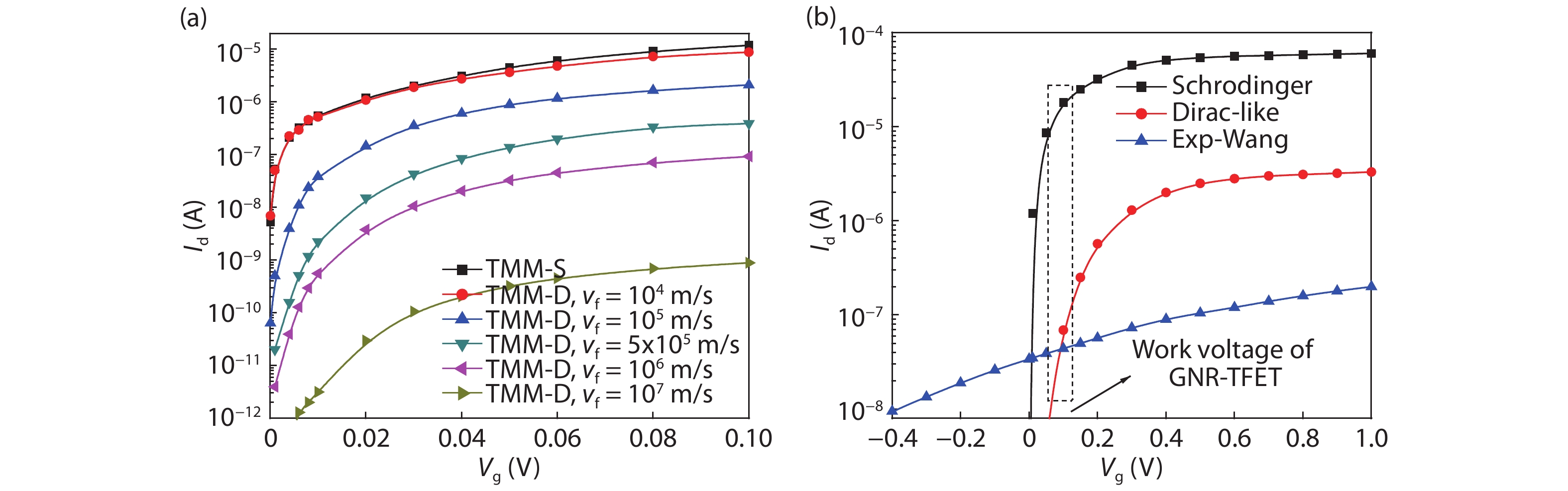
The tunneling current in a graphene nanoribbon tunnel field effect transistor (GNR-TFET) has been quantum mechanically modeled. The tunneling current in the GNR-TFET was compared based on calculations of the Dirac-like equation and Schrödinger's equation. To calculate the electron transmittance, a numerical approach-namely the transfer matrix method (TMM)-was employed and the Launder formula was used to compute the tunneling current. The results suggest that the tunneling currents that were calculated using both equations have similar characteristics for the same parameters, even though they have different values. The tunneling currents that were calculated by applying the Dirac-like equation were lower than those calculated using Schrödinger's equation.

J. Semicond.
2019, 40(6): 062003 doi: 10.1088/1674-4926/40/6/062003
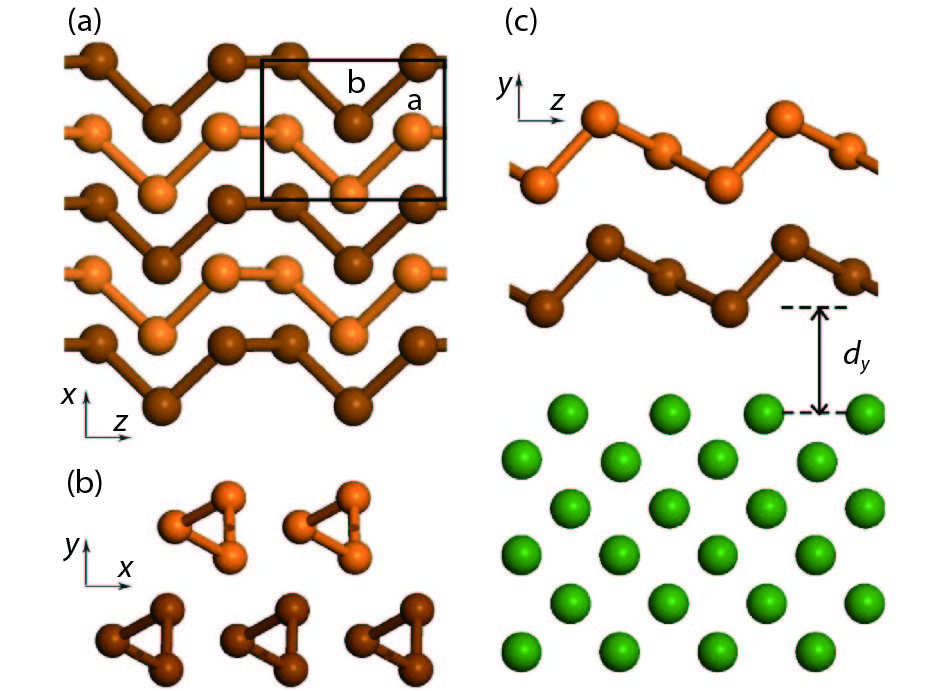
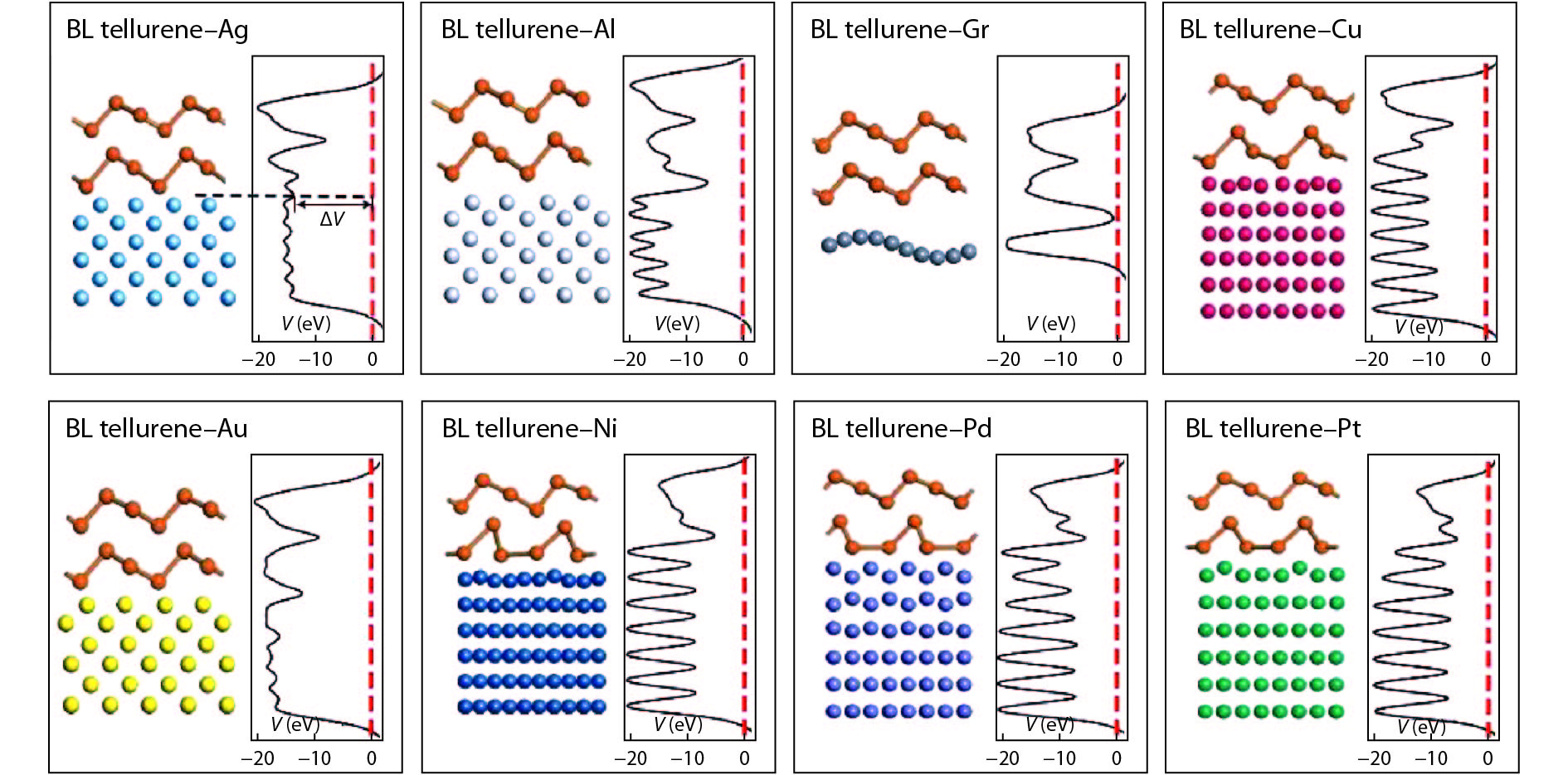
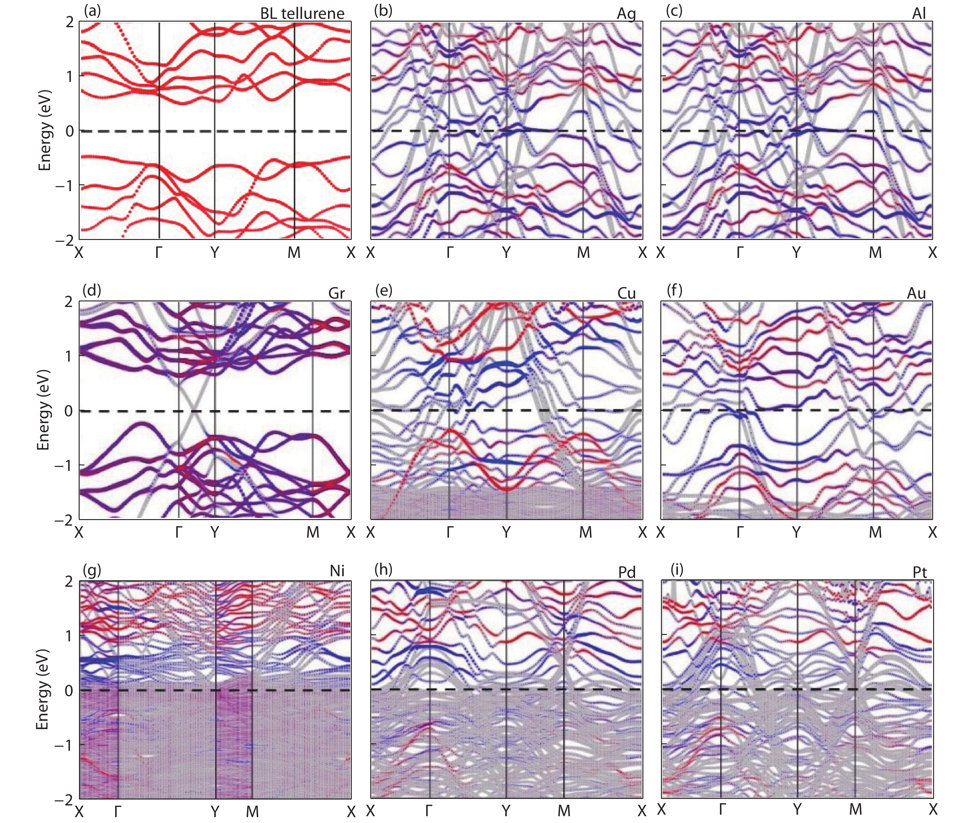
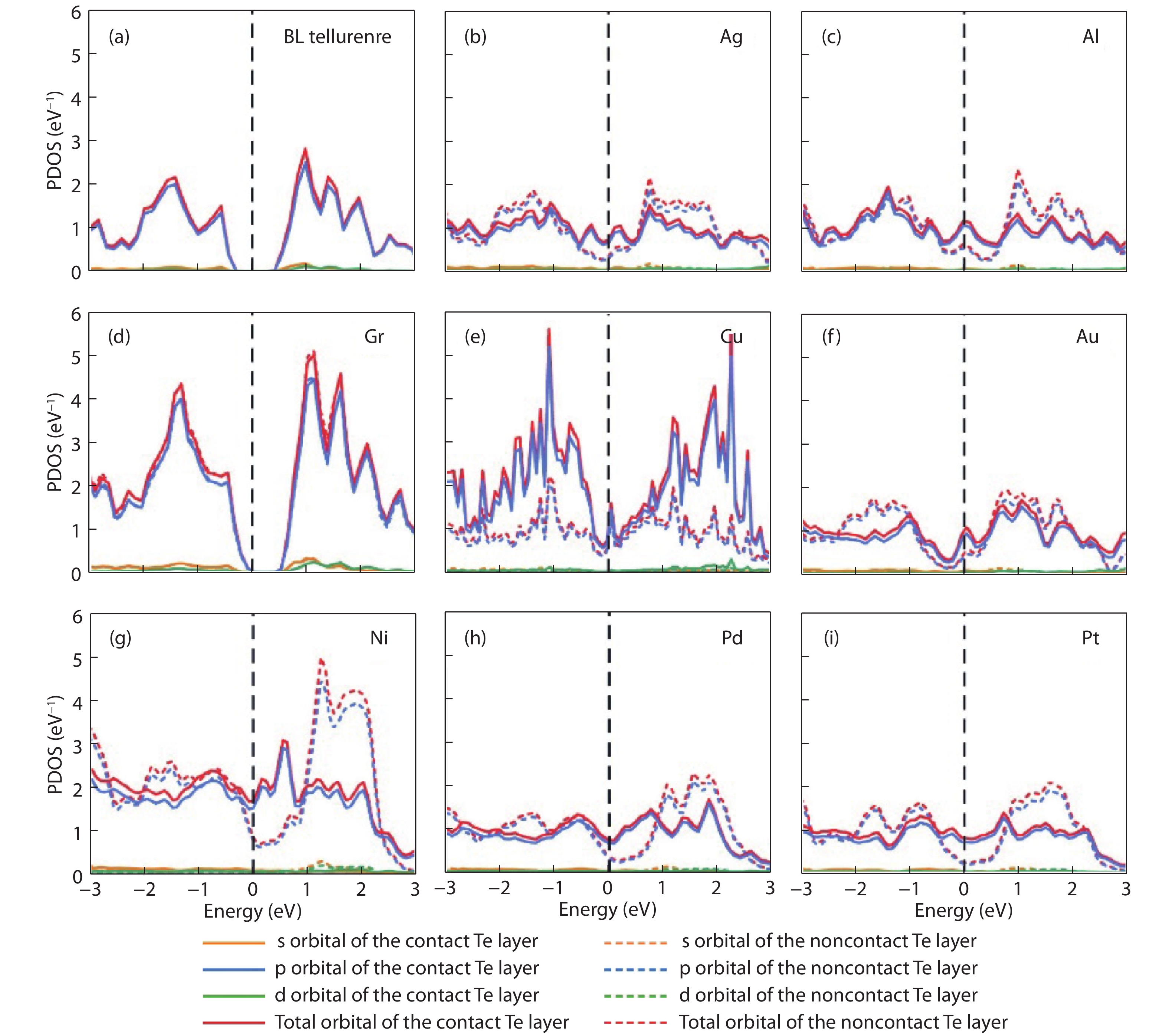
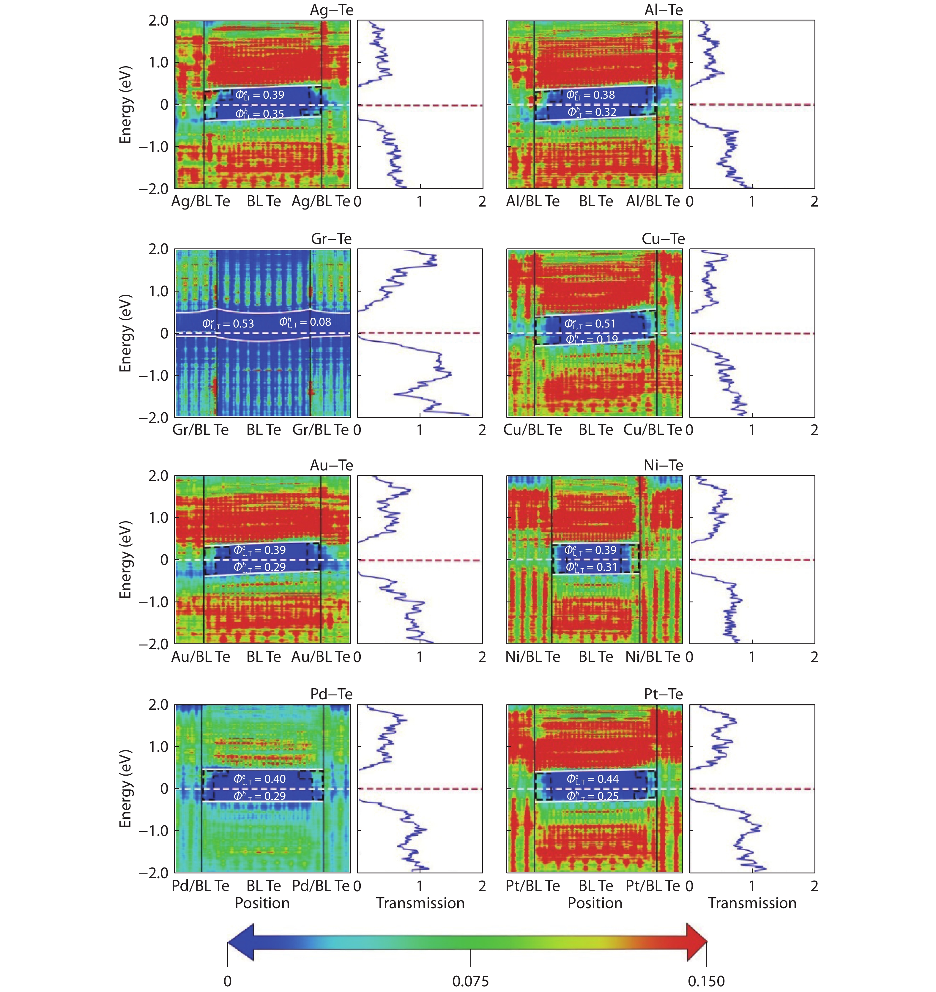
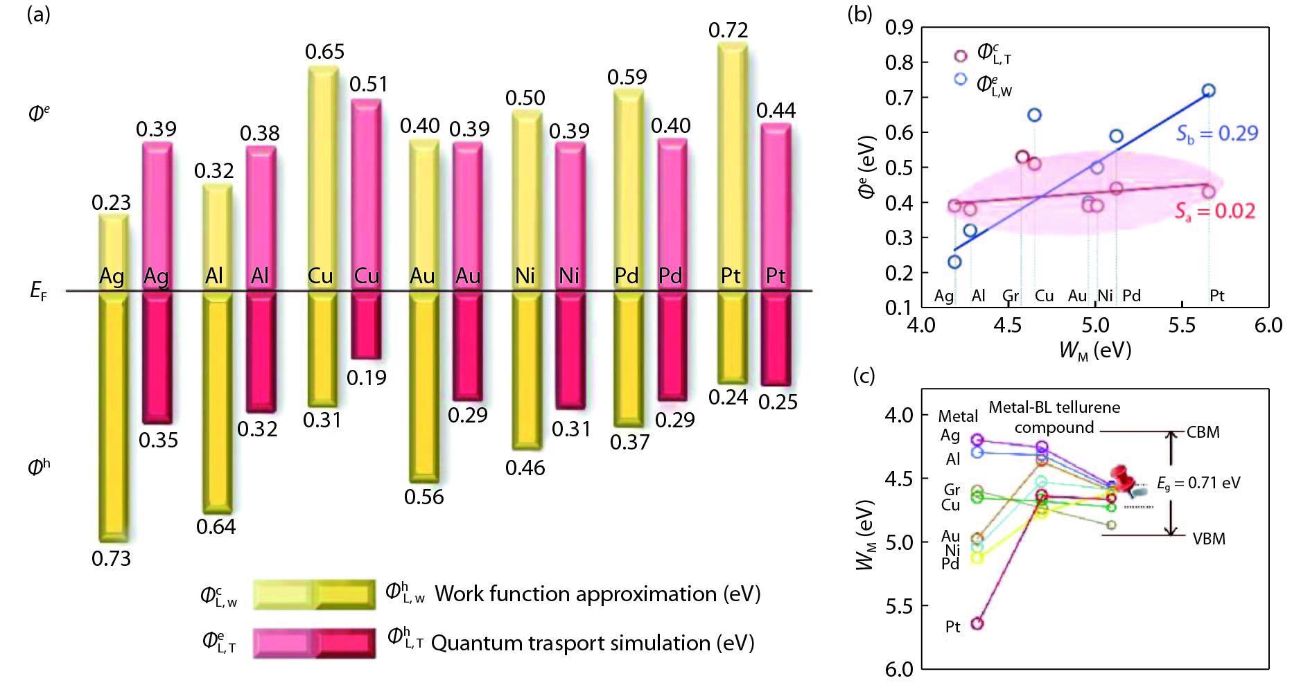
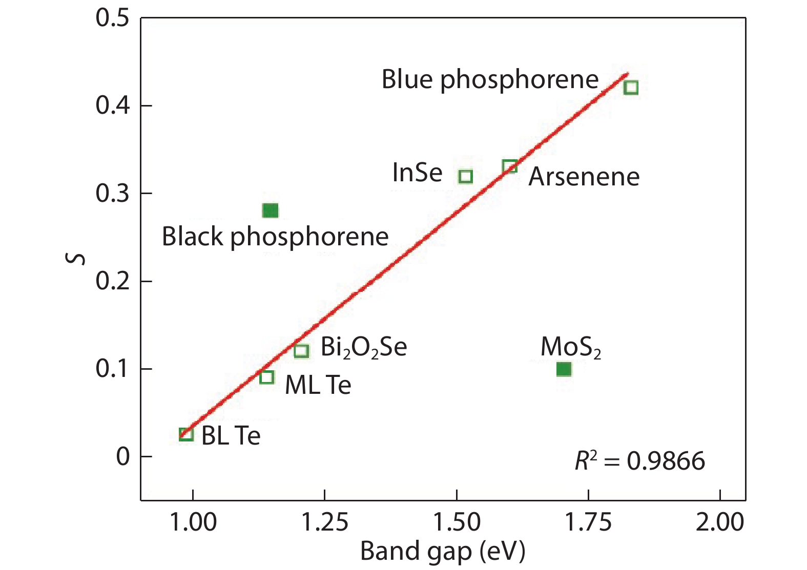
Tellurene, an emerging two-dimensional chain-like semiconductor, stands out for its high switch ratio, carrier mobility and excellent stability in air. Directly contacting the 2D semiconductor materials with metal electrodes is a feasible doping means to inject carriers. However, Schottky barrier often arises at the metal–semiconductors interface, impeding the transport of carriers. Herein, we investigate the interfacial properties of BL tellurene by contacting with various metals including graphene by using ab initio calculations and quantum transport simulations. Vertical Schottky barriers take place in Ag, Al, Au and Cu electrodes according to the maintenance of the noncontact tellurene layer band structure. Besides, a p-type vertical Schottky contact is formed due to the van der Waals interaction for graphene electrode. As for the lateral direction, p-type Schottky contacts take shape for bulk metal electrodes (hole Schottky barrier heights (SBHs) ranging from 0.19 to 0.35 eV). Strong Fermi level pinning takes place with a pinning factor of 0.02. Notably, a desirable p-type quasi-Ohmic contact is developed for graphene electrode with a hole SBH of 0.08 eV. Our work sheds light on the interfacial properties of BL tellurene based transistors and could guide the experimental selections on electrodes.

J. Semicond.
2019, 40(6): 062004 doi: 10.1088/1674-4926/40/6/062004
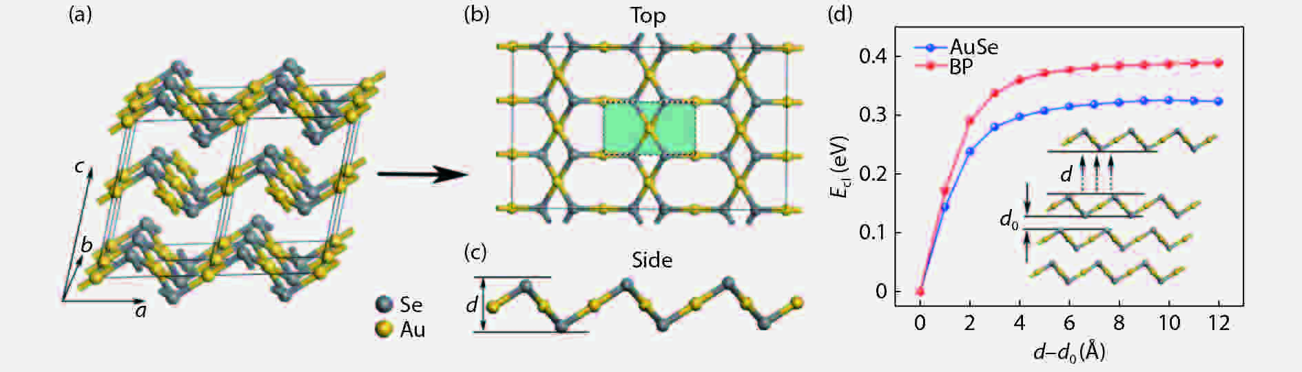
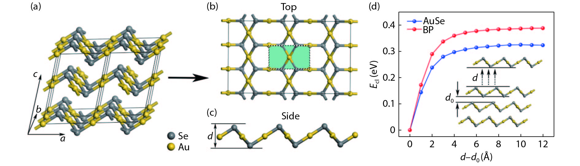
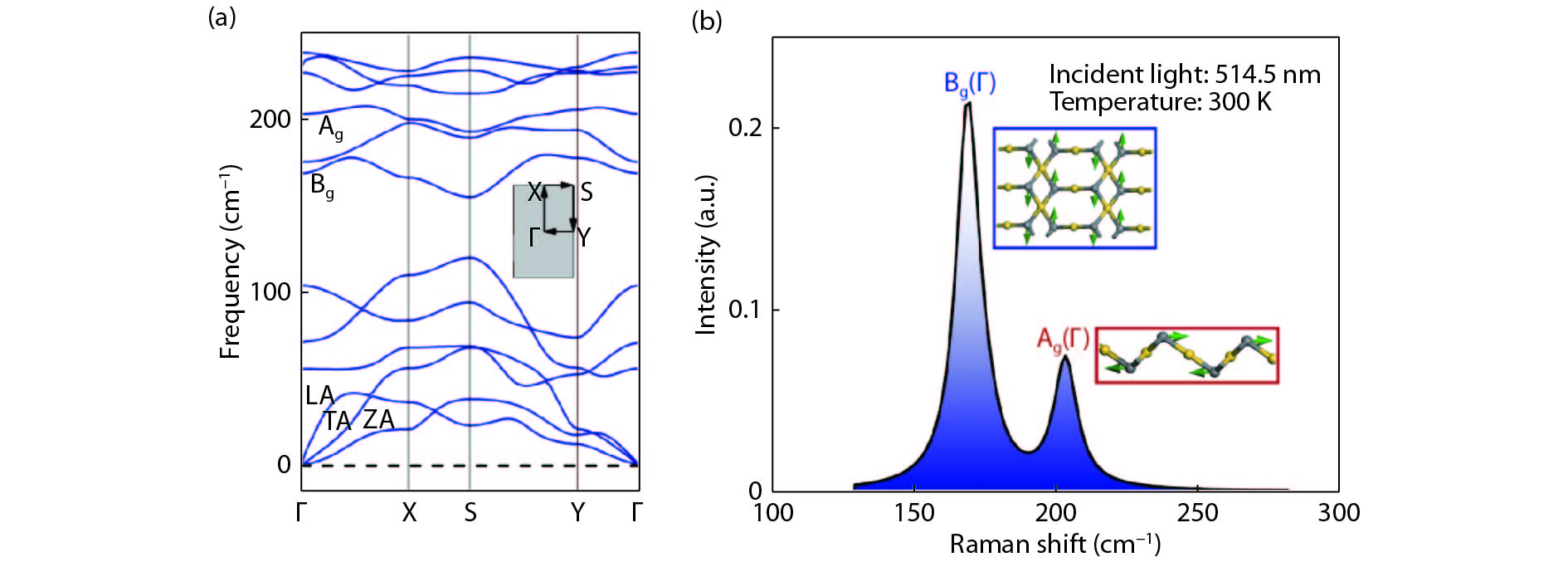
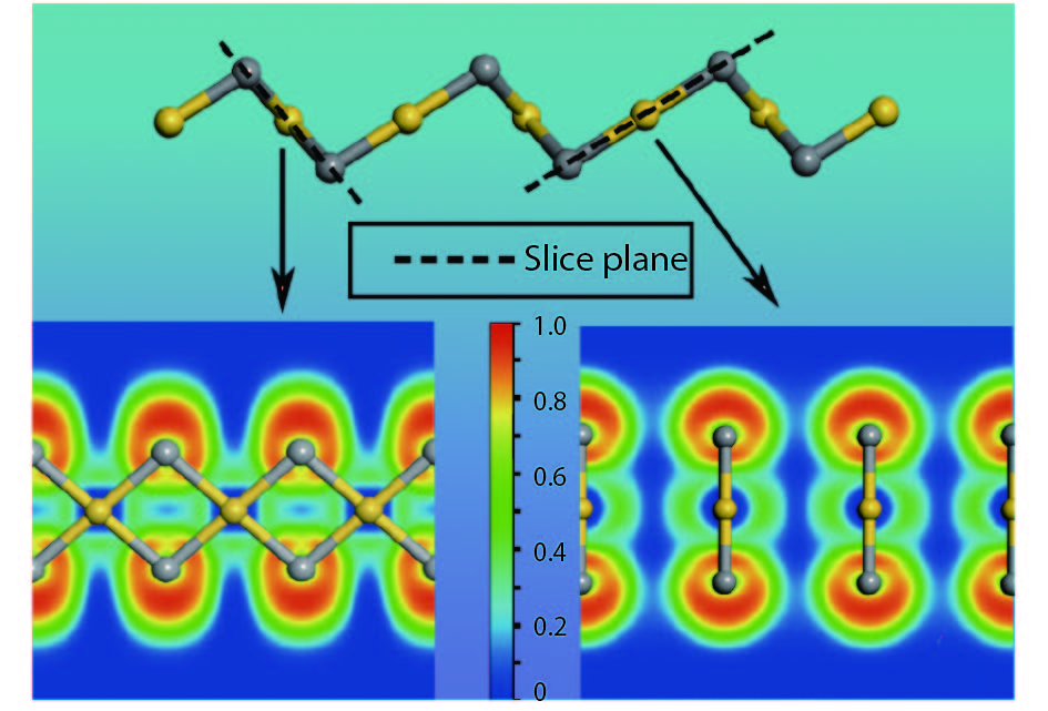
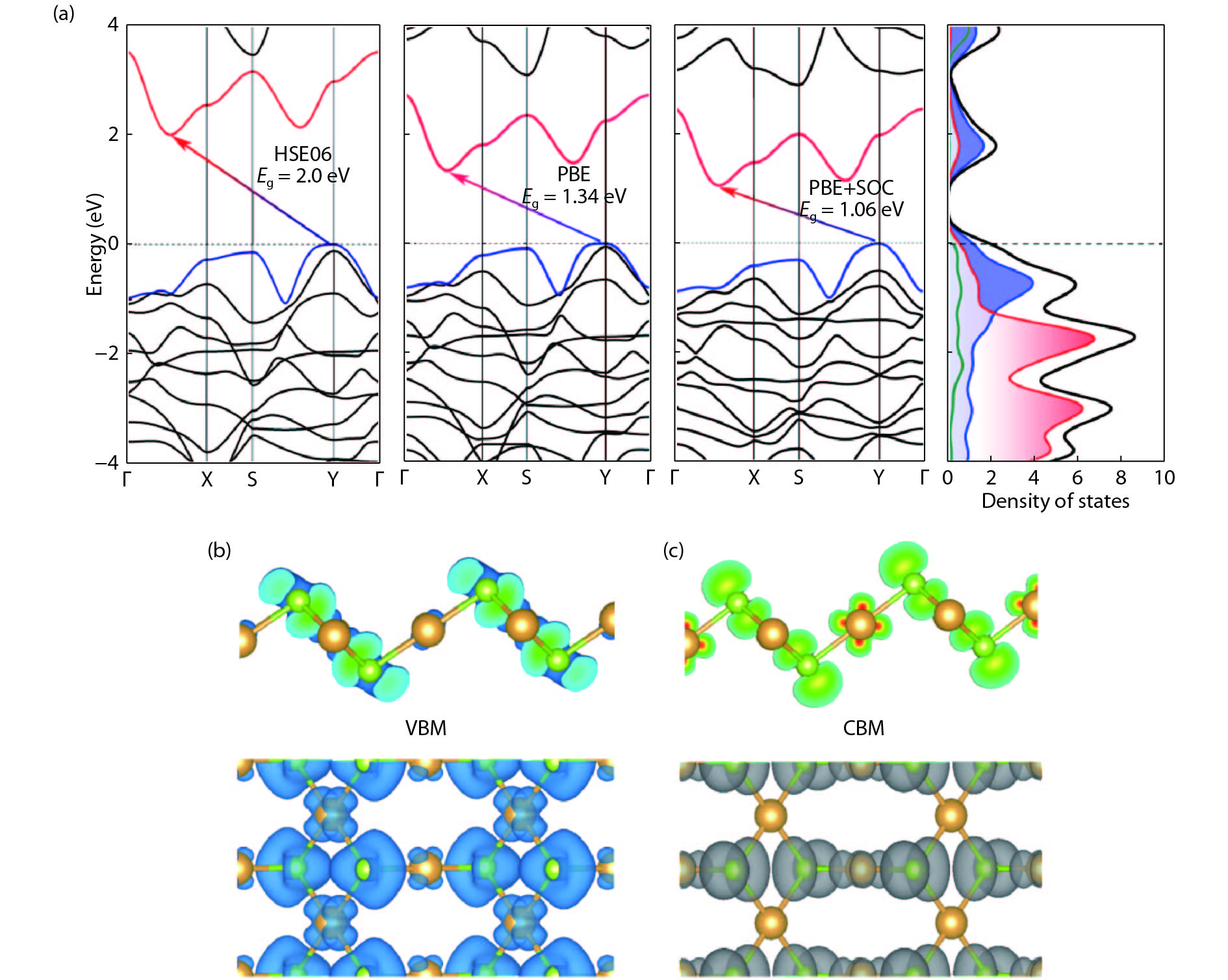
As a large family of 2D materials, transition metal dichalcogenides (TMDs) have stimulated numerous works owing to their attractive properties. The replacement of constituent elements could promote the discovery and fabrication of new nano-film in this family. Using precious metals, such as platinum and palladium, to serve as transition metals combined with chalcogen is a new approach to explore novel TMDs. Also, the proportion between transition metal and chalcogen atoms is found not only to exist in conventional form of 1 : 2. Herein, we reported a comprehensive study of a new 2D precious metal selenide, namely AuSe monolayer. Based on density functional theory, our result indicated that AuSe monolayer is a semiconductor with indirect band-gap of 2.0 eV, which possesses superior dynamic stability and thermodynamic stability with cohesive energy up to –7.87 eV/atom. Moreover, it has been confirmed that ionic bonding predominates in Au–Se bonds and absorption peaks in all directions distribute in the deep ultraviolet region. In addition, both vibration modes dominating marked Raman peaks are parallel to the 2D plane.
J. Semicond.
2019, 40(6): 062005 doi: 10.1088/1674-4926/40/6/062005
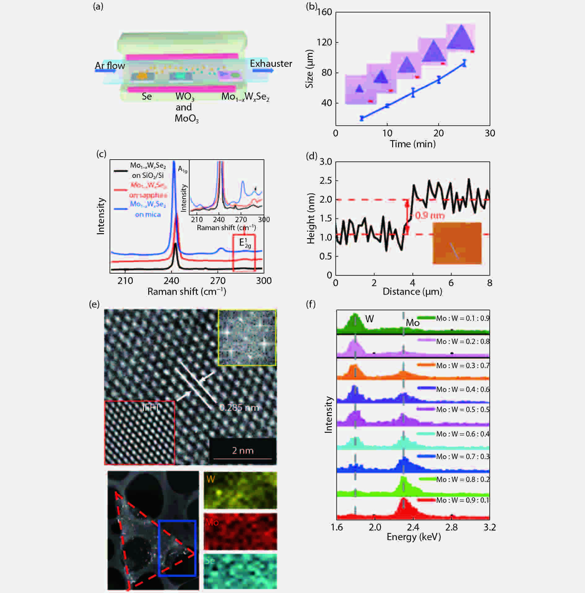
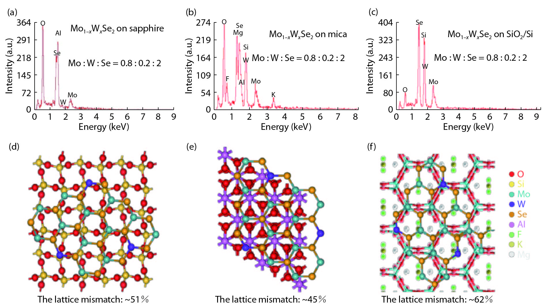
Two-dimensional (2D) transition metal dichalcogenides alloys are potential materials in the application of photodetectors over a wide spectral range due to their composition-dependent bandgaps. The study of bandgap engineering is important for the application of 2D materials in devices. Here, we grow the Mo1−xWxSe2 alloys on mica, sapphire and SiO2/Si substrates by chemical vapor deposition (CVD) method. Mo1−xWxSe2 alloys are grown on the mica substrates by CVD method for the first time. Photoluminescence (PL) spectroscopy is used to investigate the effects of substrates and interlayer coupling force on the optical bandgaps of as-grown Mo1−xWxSe2 alloys. We find that the substrates used in this work have an ignorable effect on the optical bandgaps of as-grown Mo1−xWxSe2. The interlayer coupling effect on the optical bandgaps of as-grown Mo1−xWxSe2 is larger than the substrates effect. These findings provide a new way for the future study of the growth and physical properties of 2D alloy materials.


J. Semicond.
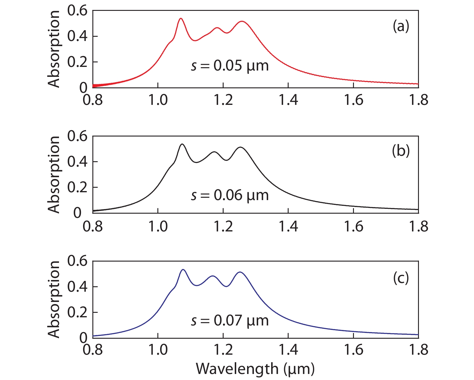
2019, 40(6): 062006 doi: 10.1088/1674-4926/40/6/062006

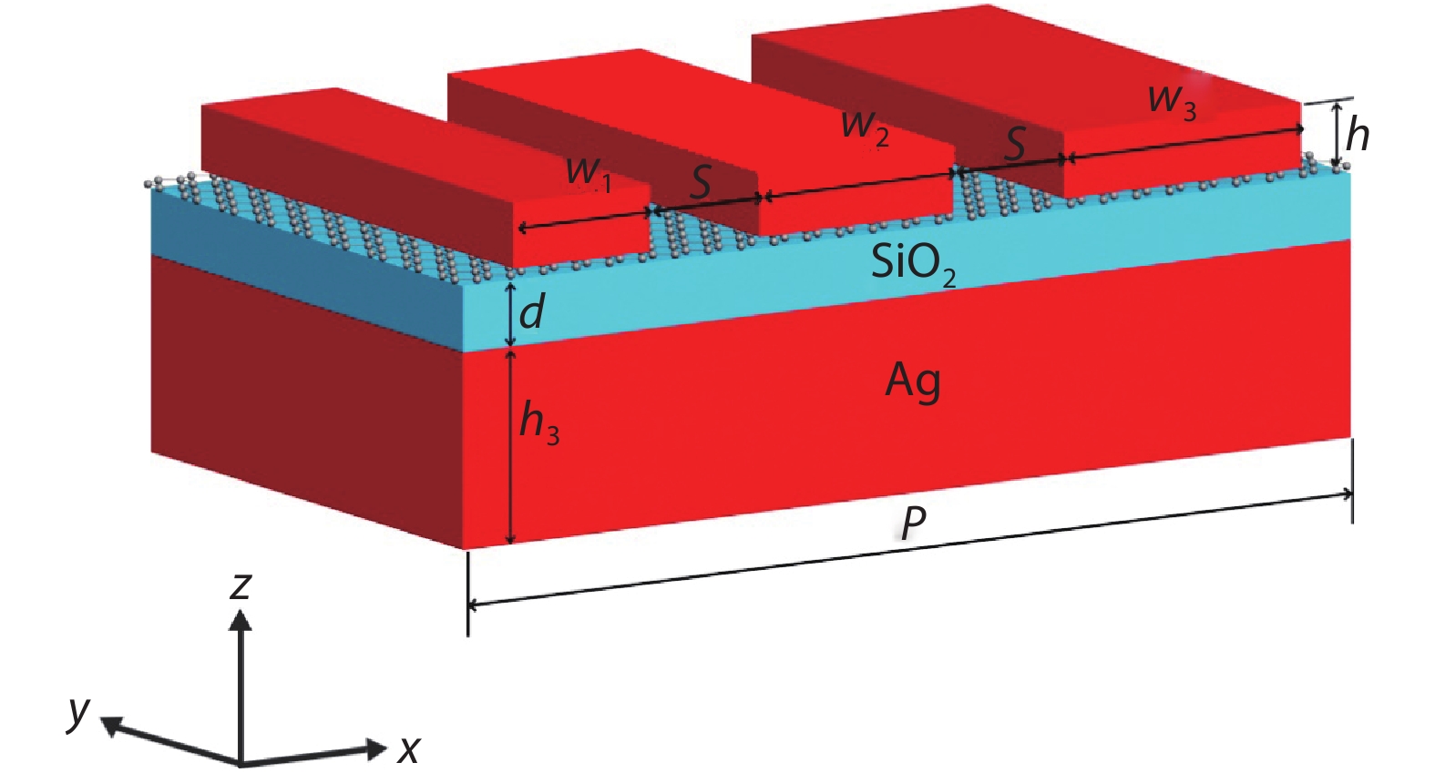
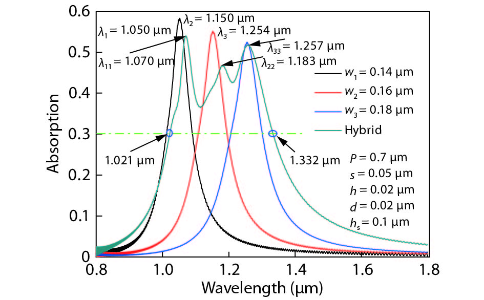
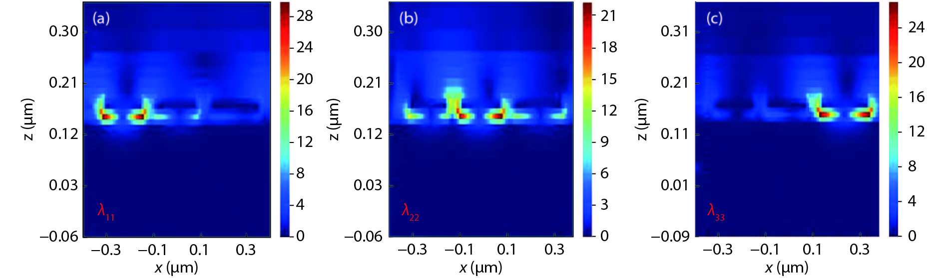
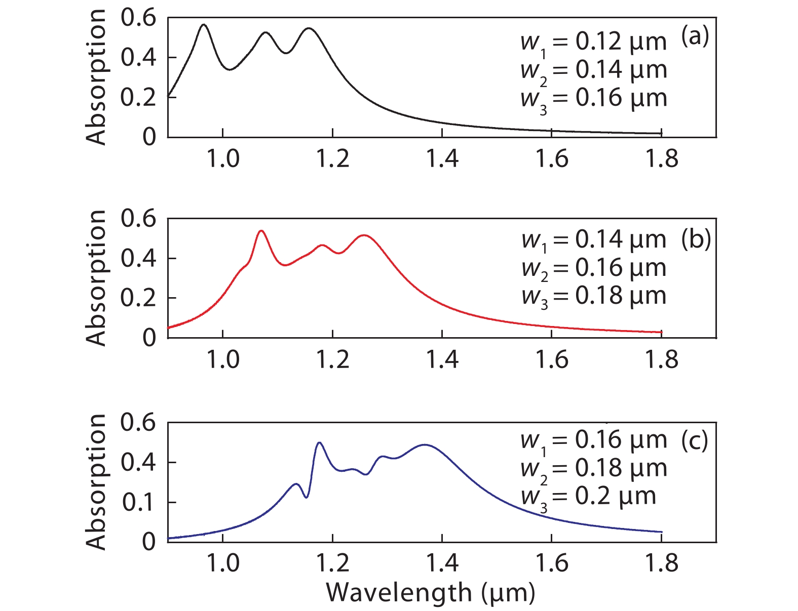
As emerging new material, graphene has inspired great research interest. However, most of the studies focused on how to improve the absorption efficiency of graphene, but payed little attention on broadening absorption bandwidth while ensuring high absorption efficiency. In this work, we proposed a hybrid nanostructure, which not only can improve absorption efficiency but also can increase absorption bandwidth. The proposed hybrid nanostructure consists of a monolayer graphene sandwiched between three Ag gratings with different widths and a SiO2 spacer on a Ag substrate, these three gratings and substrate can excite three independent magnetic dipole resonances. In our calculations, we numerically demonstrate the proposed hybrid structure can achieve graphene absorption bandwidth of 0.311 μm in near-infrared region with absorption exceeding 30% . We also studied absorption peaks dependence on gratings widths and SiO2 spacer thickness, and explained the results using physical mechanism. Our research can provide a theoretical guidance for future device preparation.