Issue Browser
Volume 41, Issue 3,
Mar 2020
Column
J. Semicond.
2020, 41(3): 032101 doi: 10.1088/1674-4926/41/3/032101
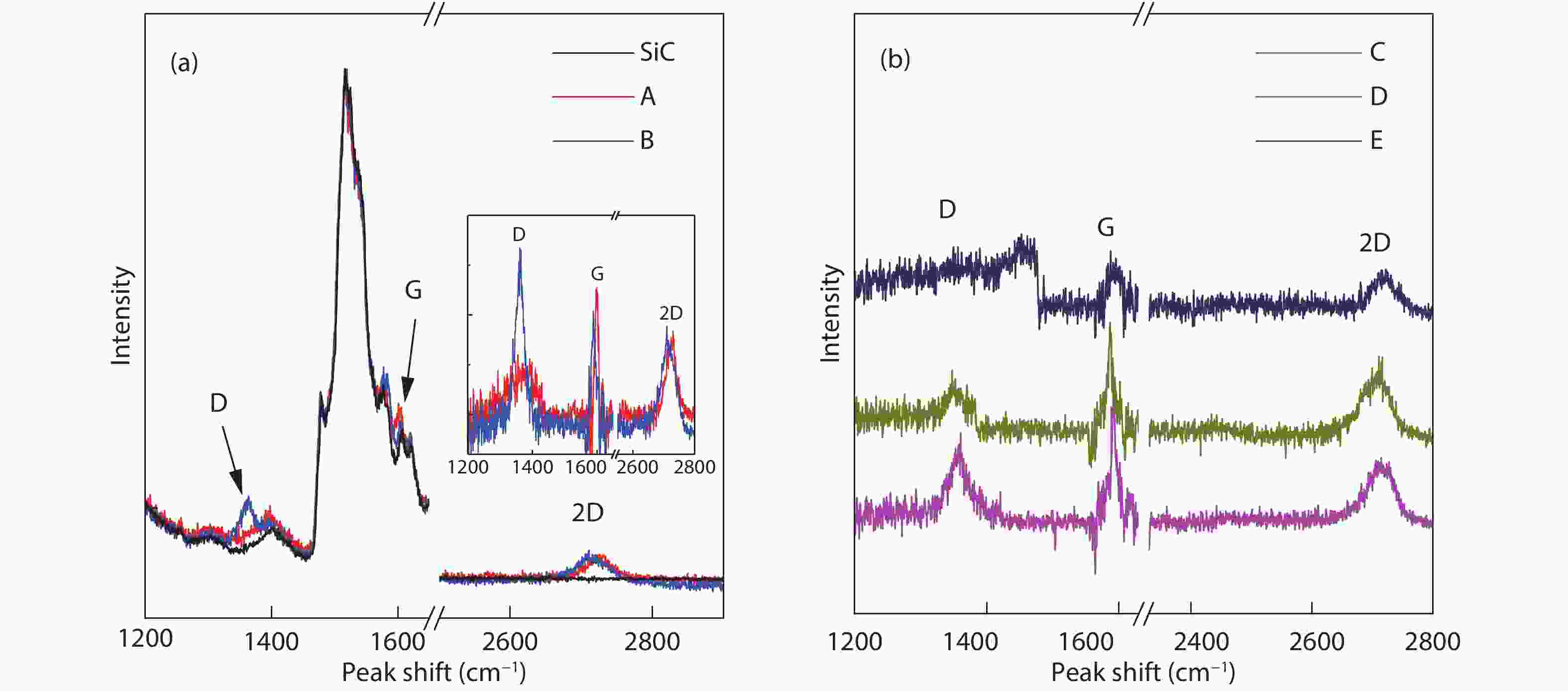
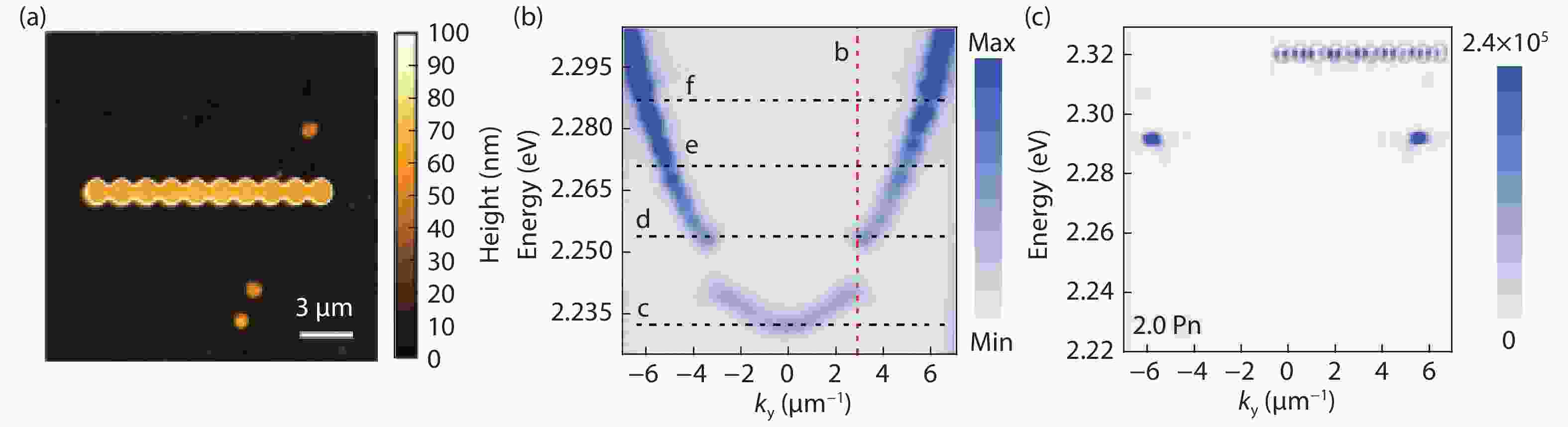
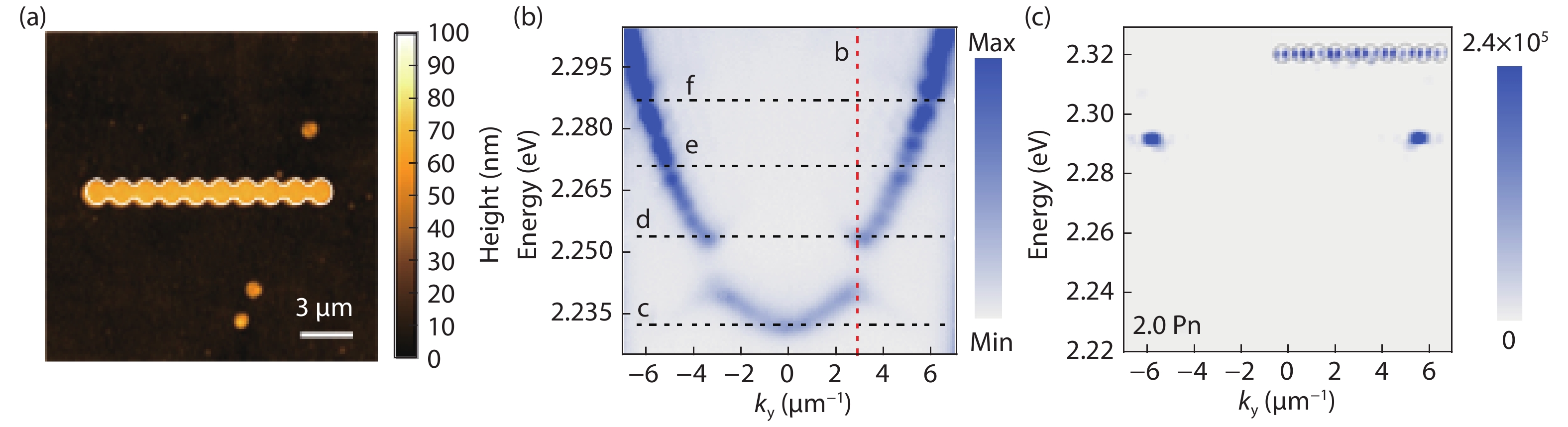
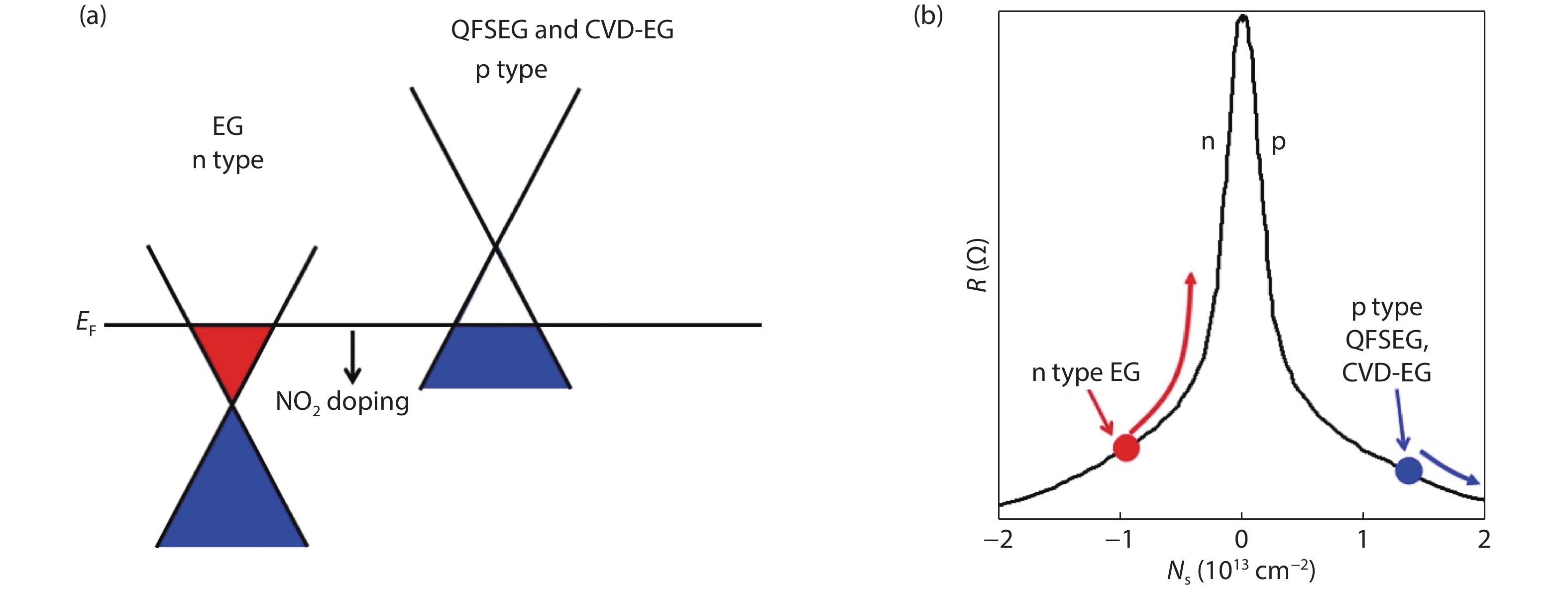
2D material of graphene has inspired huge interest in fabricating of solid state gas sensors. In this work, epitaxial graphene, quasi-free-standing graphene, and CVD epitaxial graphene samples on SiC substrates are used to fabricate gas sensors. Defects are introduced into graphene using SF6 plasma treatment to improve the performance of the gas sensors. The epitaxial graphene shows high sensitivity to NO2 with response of 105.1% to 4 ppm NO2 and detection limit of 1 ppb. The higher sensitivity of epitaxial graphene compared to quasi-free-standing graphene, and CVD epitaxial graphene was found to be related to the different doping types of the samples.

J. Semicond.
2020, 41(3): 032102 doi: 10.1088/1674-4926/41/3/032102
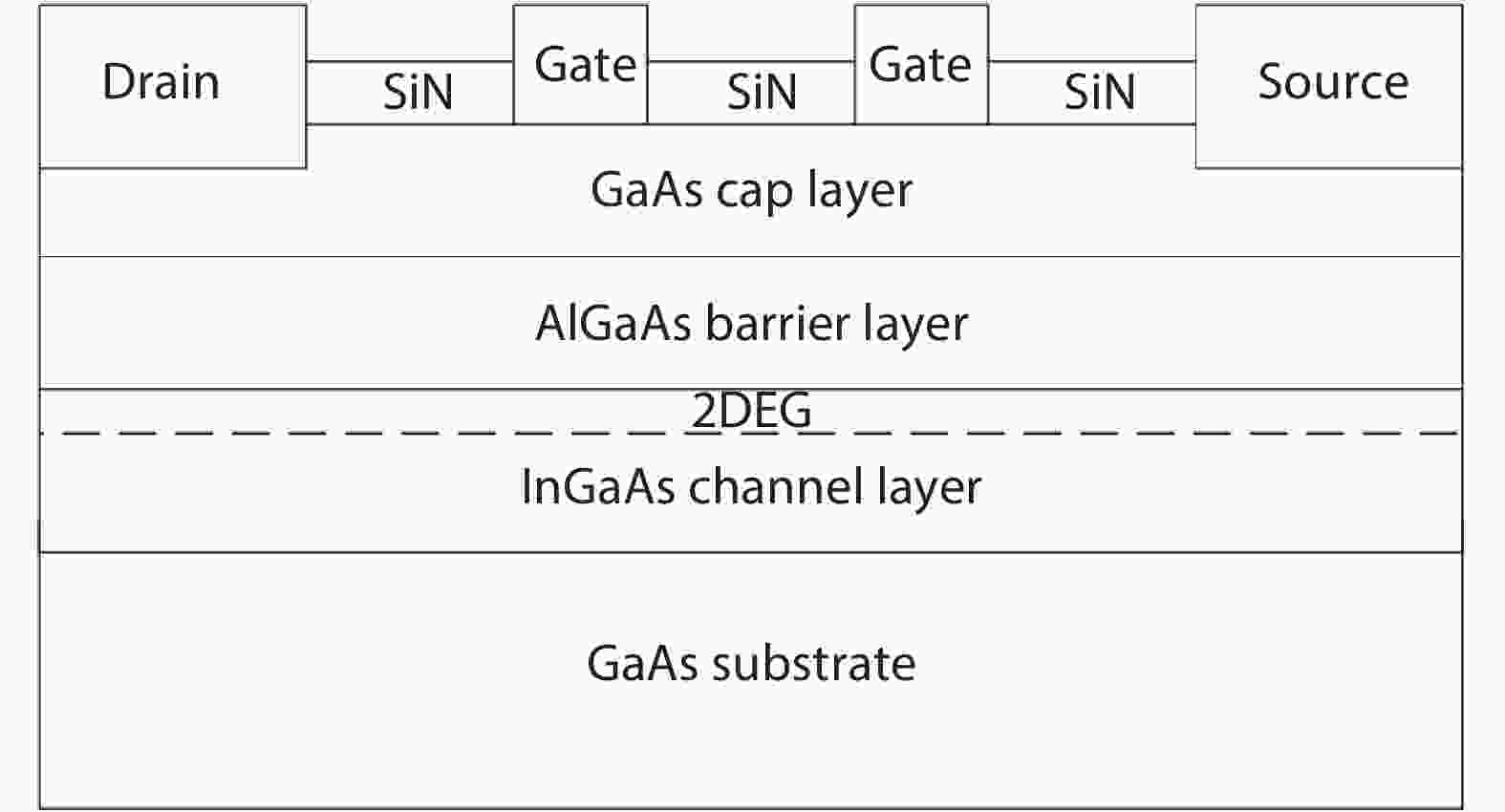
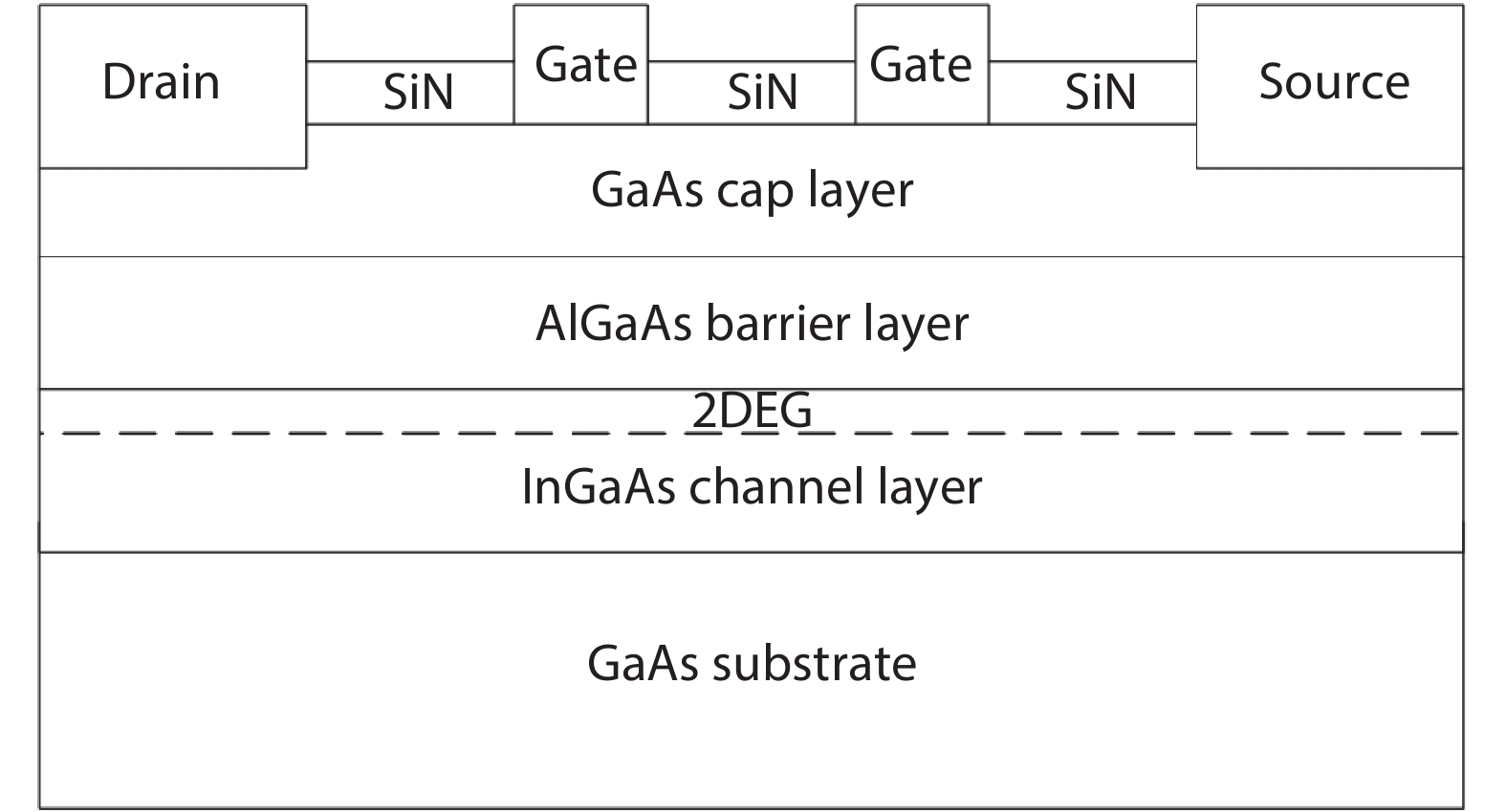
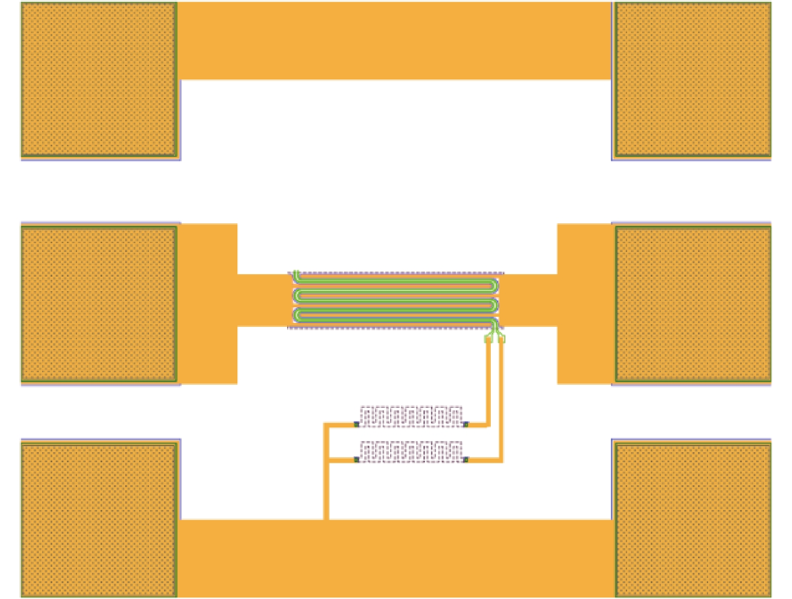
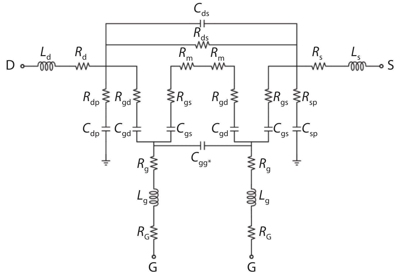
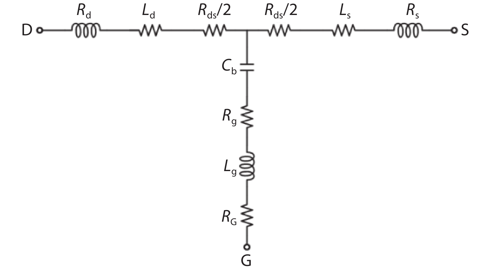
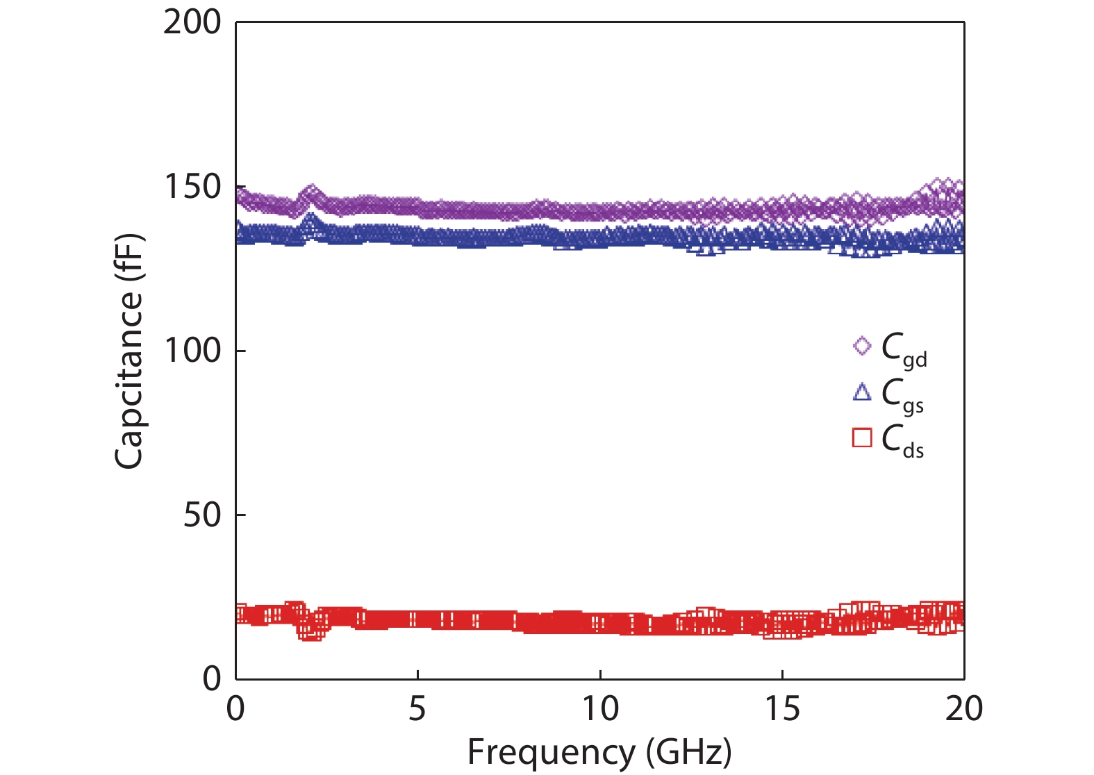
This paper presents an accurate small-signal model for multi-gate GaAs pHEMTs in switching-mode. The extraction method for the proposed model is developed. A 2-gate switch structure is fabricated on a commercial 0.5 μm AlGaAs/GaAs pHEMT technology to verify the proposed model. Excellent agreement has been obtained between the measured and simulated results over a wide frequency range.


J. Semicond.
2020, 41(3): 032103 doi: 10.1088/1674-4926/41/3/032103

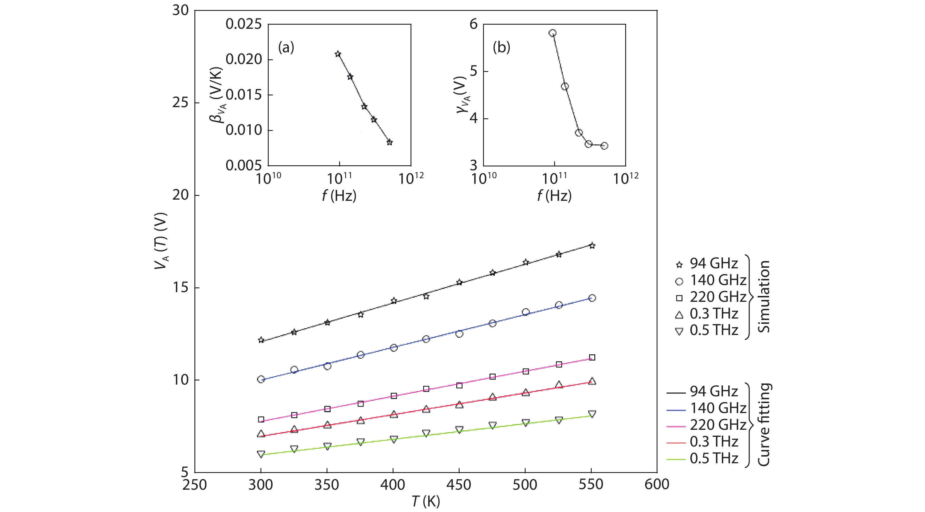
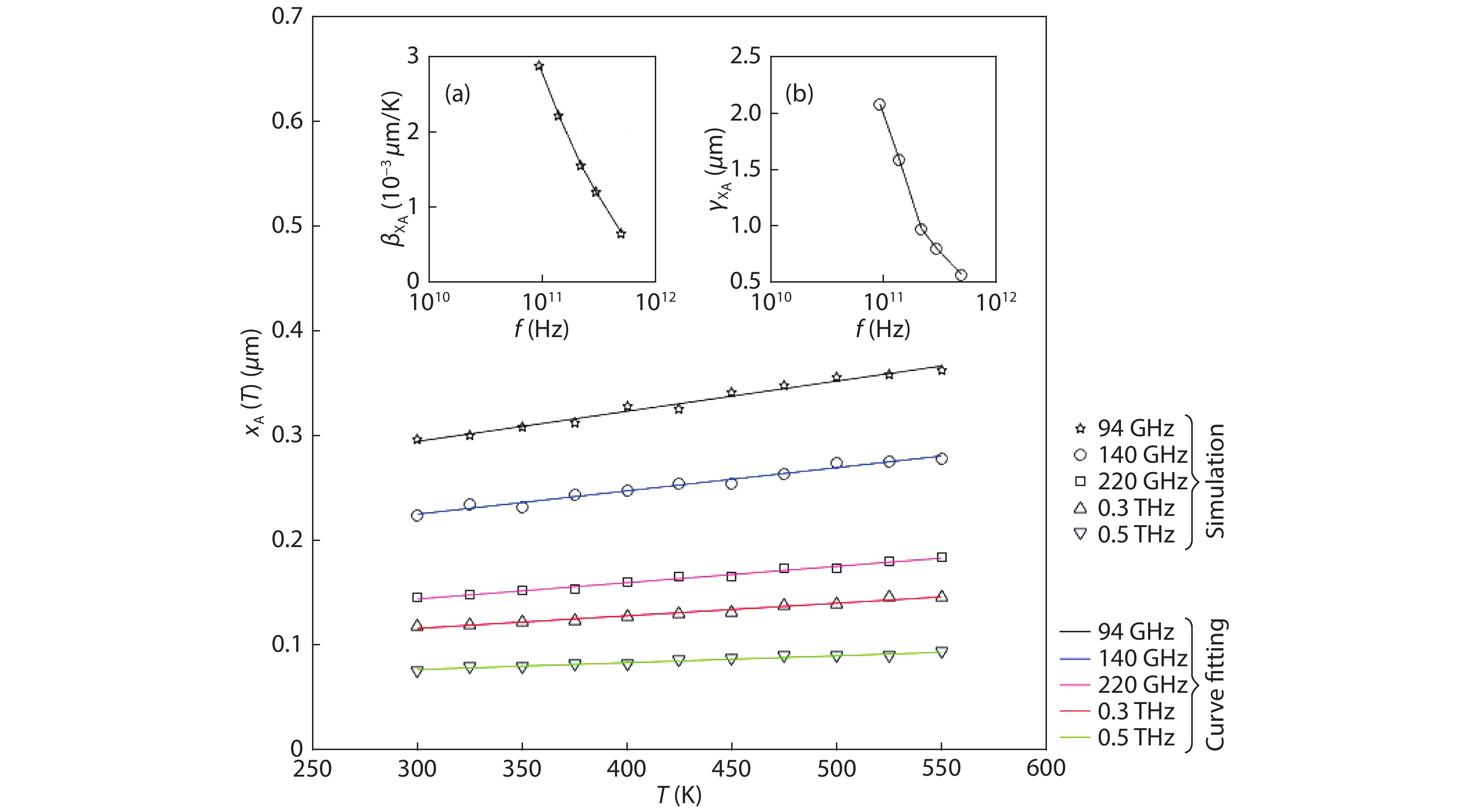
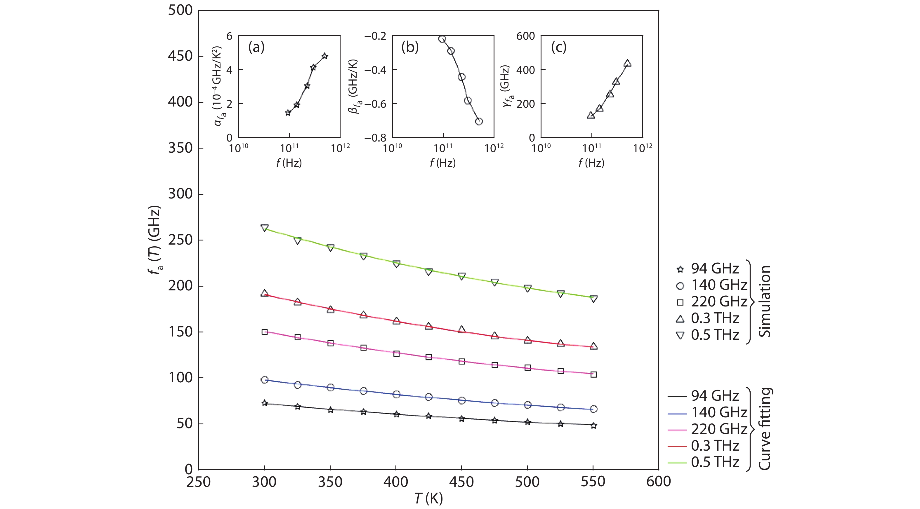
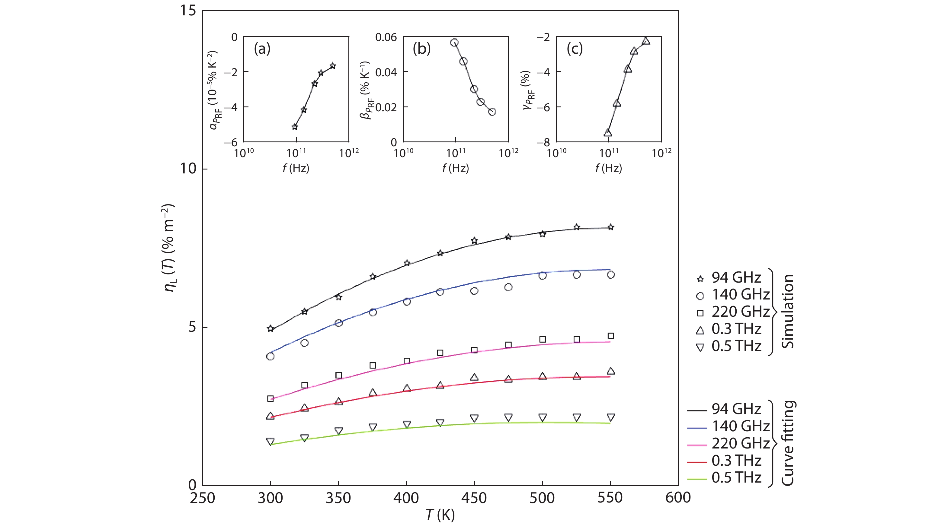
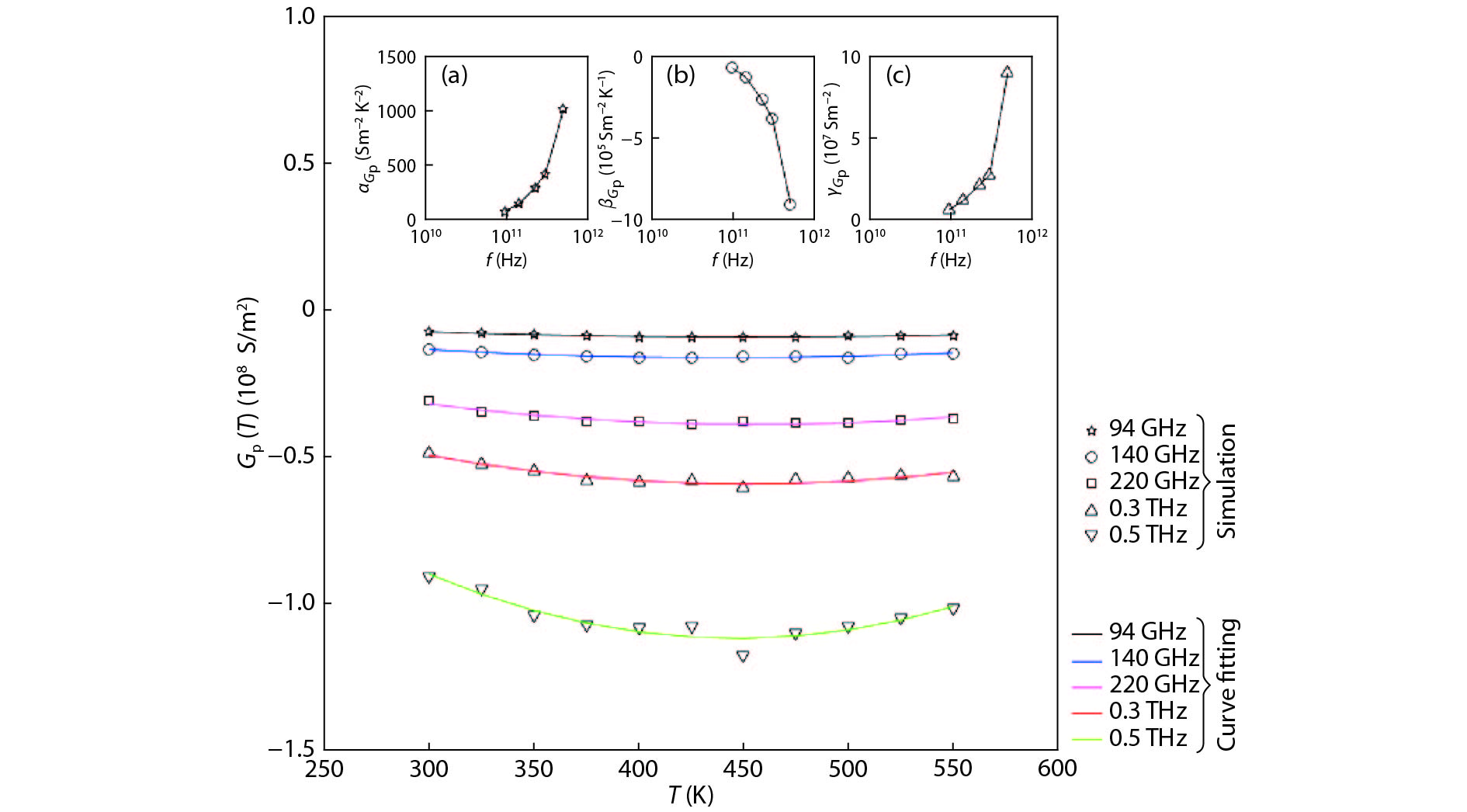
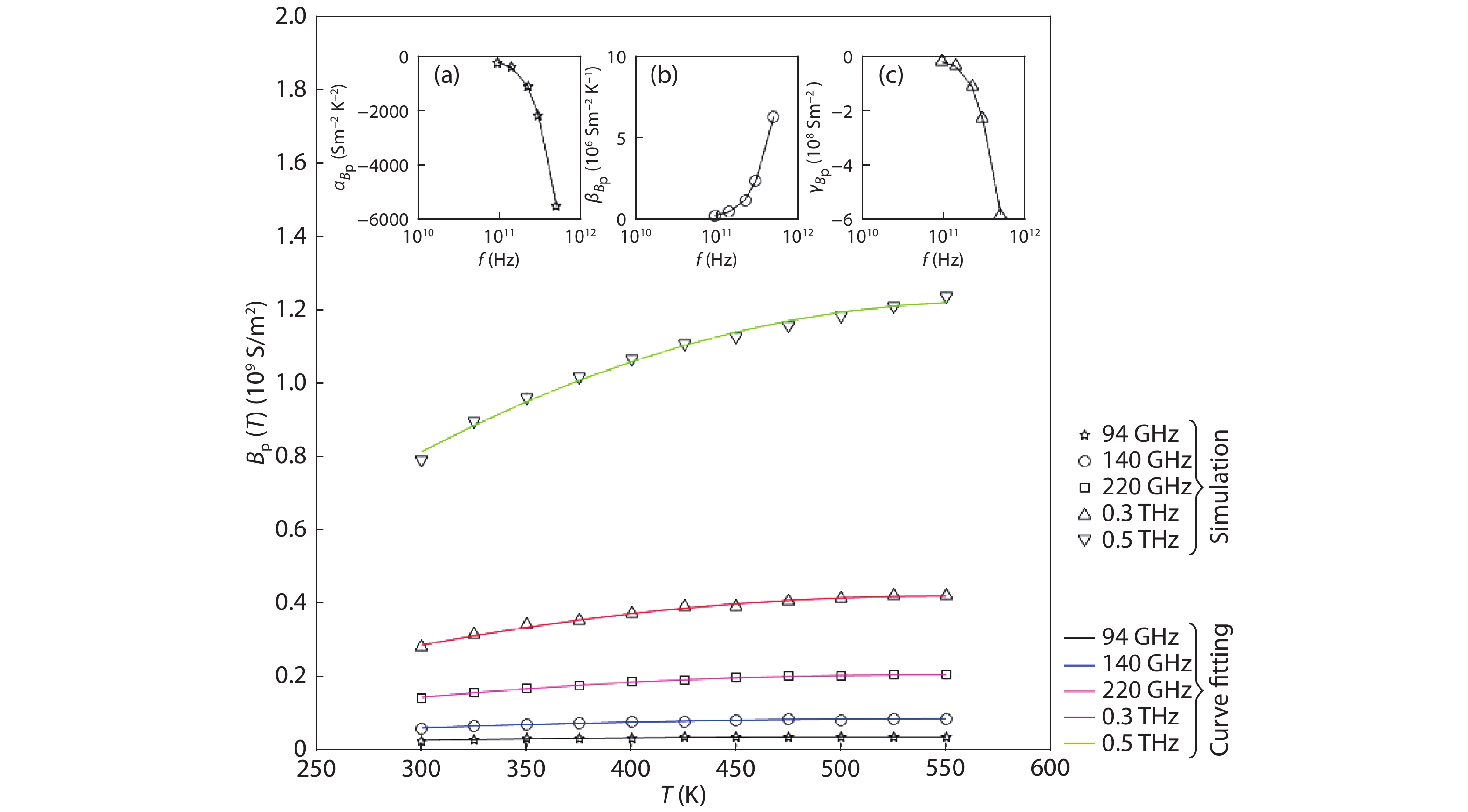
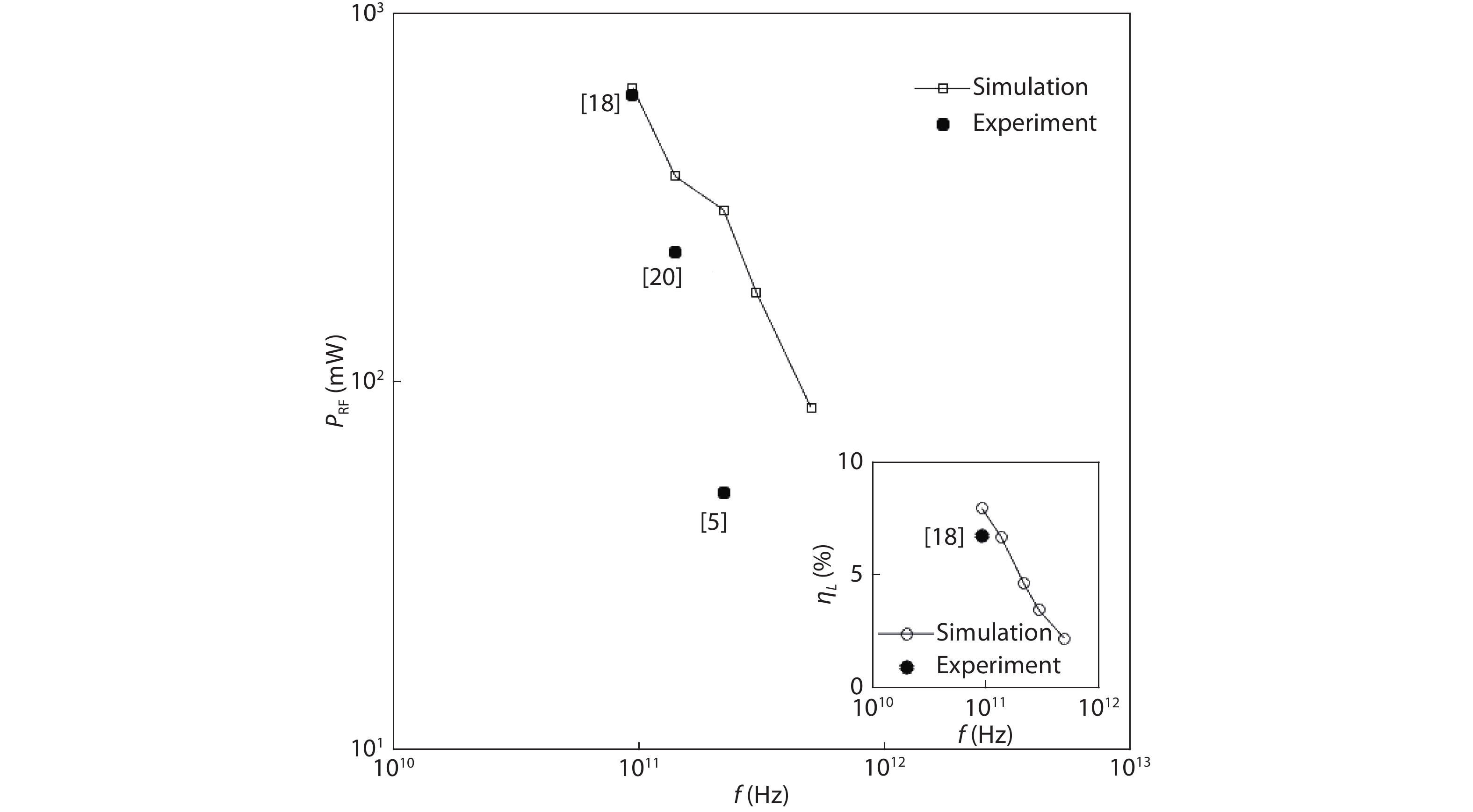
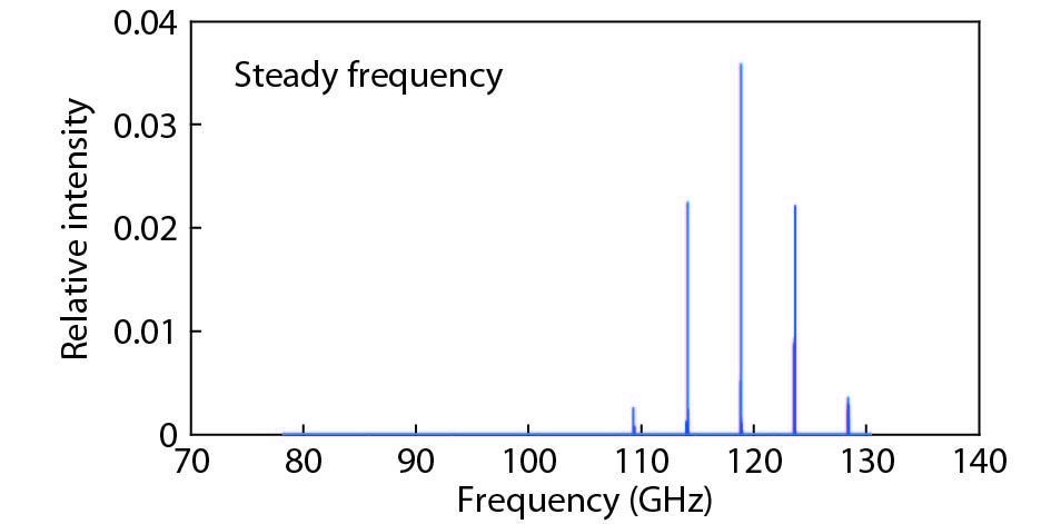
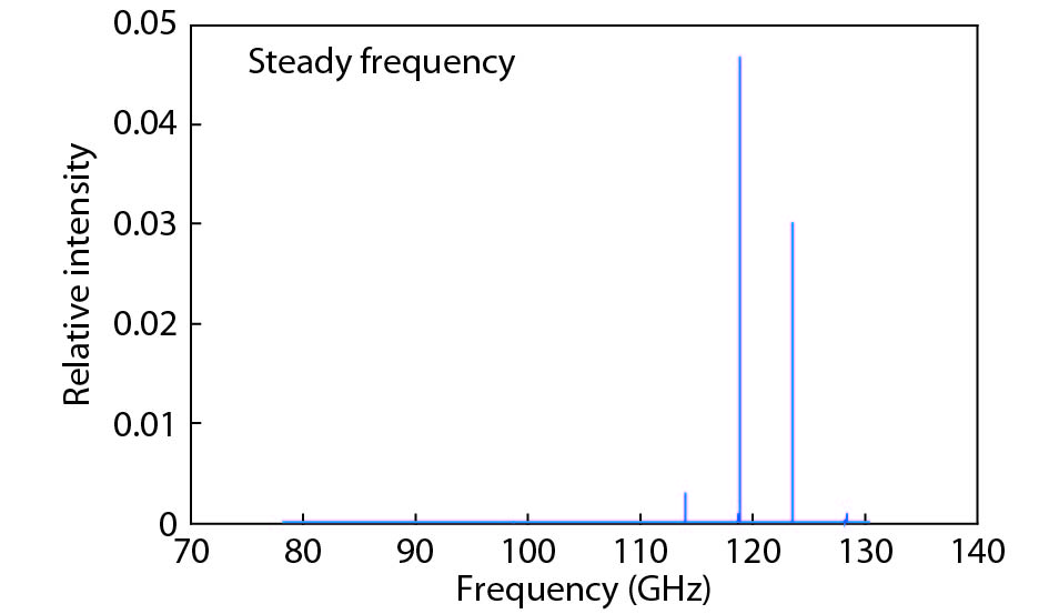
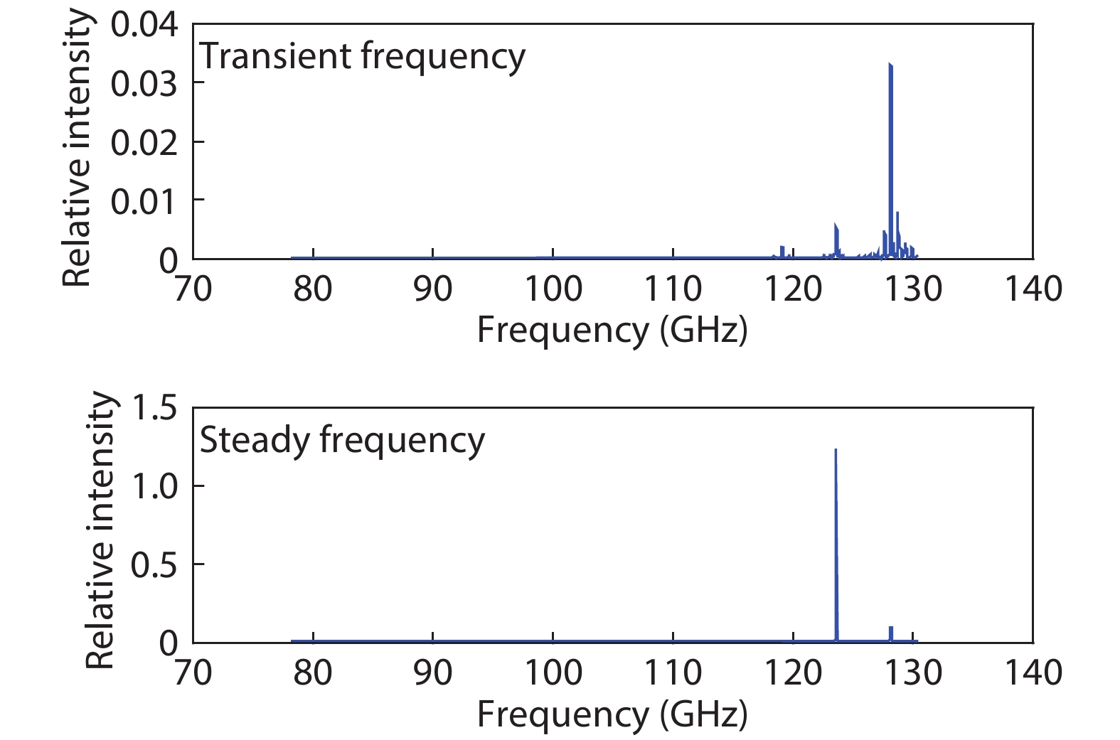
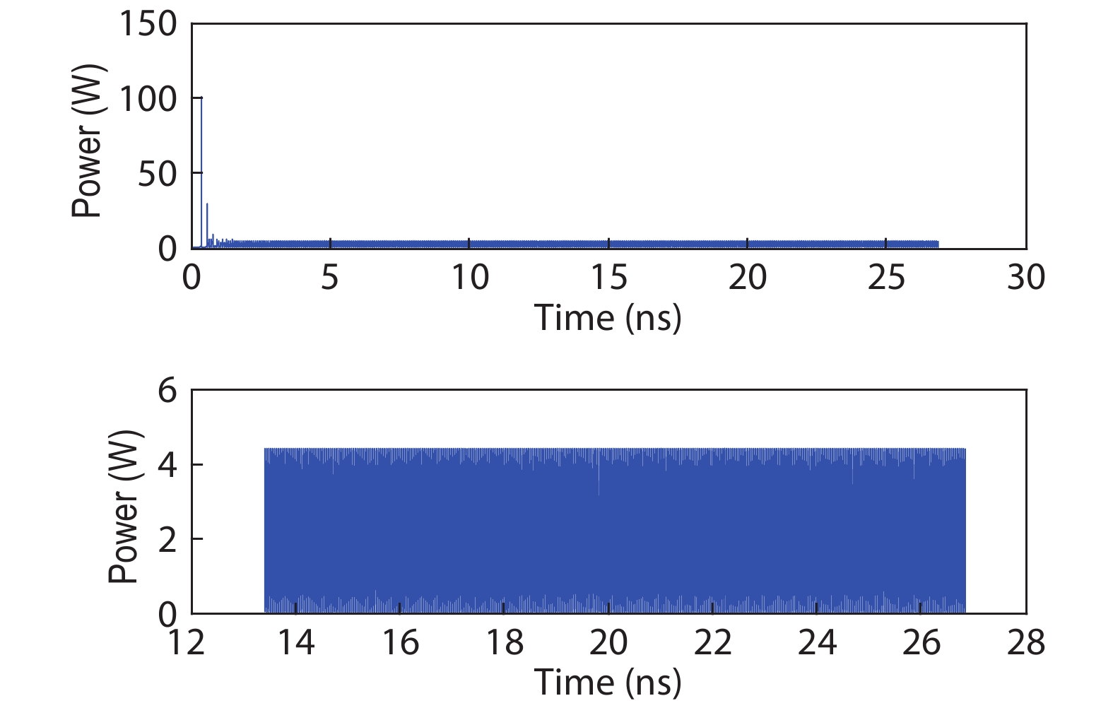
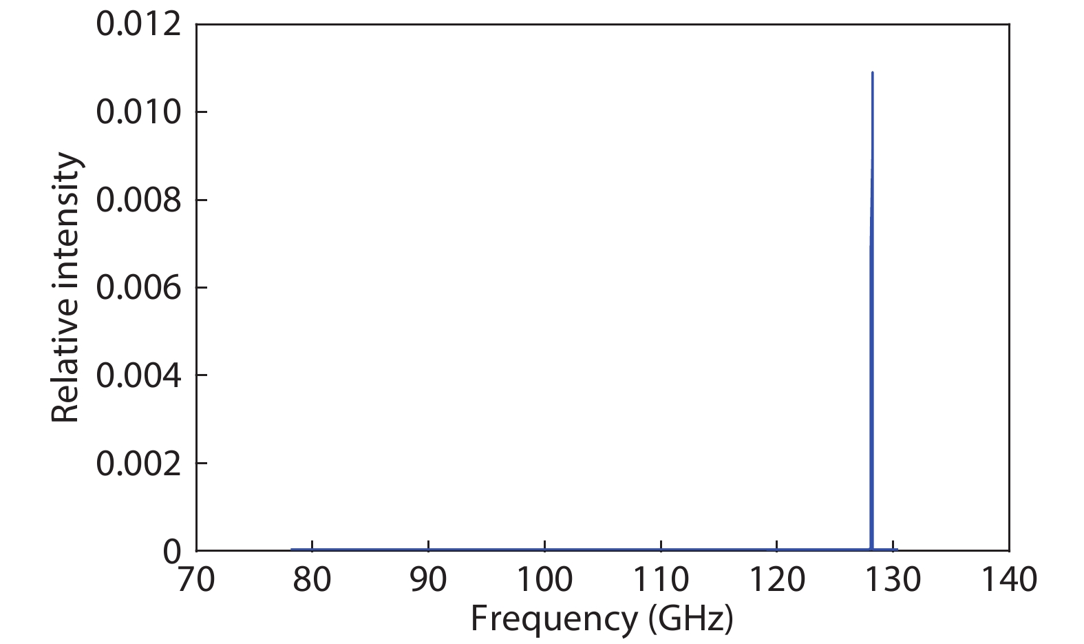
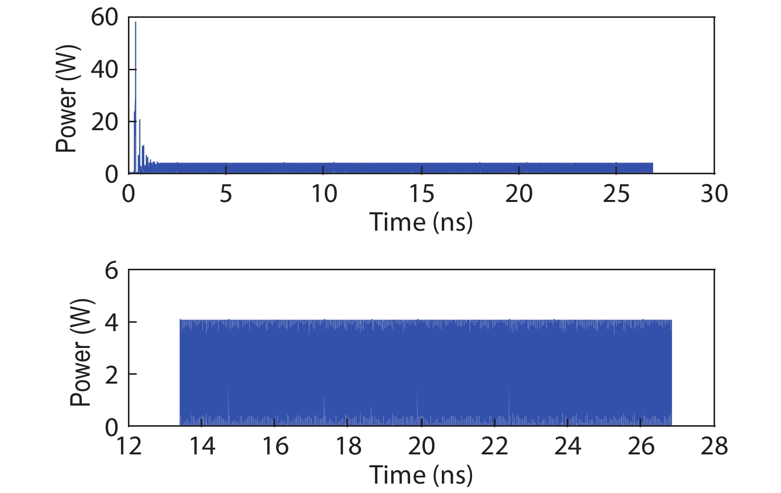
The influence of self-heating on the millimeter-wave (mm-wave) and terahertz (THz) performance of double-drift region (DDR) impact avalanche transit time (IMPATT) sources based on silicon (Si) has been investigated in this paper. The dependences of static and large-signal parameters on junction temperature are estimated using a non-sinusoidal voltage excited (NSVE) large-signal simulation technique developed by the authors, which is based on the quantum-corrected drift-diffusion (QCDD) model. Linear variations of static parameters and non-linear variations of large-signal parameters with temperature have been observed. Analytical expressions representing the temperature dependences of static and large-signal parameters of the diodes are developed using linear and 2nd degree polynomial curve fitting techniques, which will be highly useful for optimizing the thermal design of the oscillators. Finally, the simulated results are found to be in close agreement with the experimentally measured data.


J. Semicond.
2020, 41(3): 032104 doi: 10.1088/1674-4926/41/3/032104
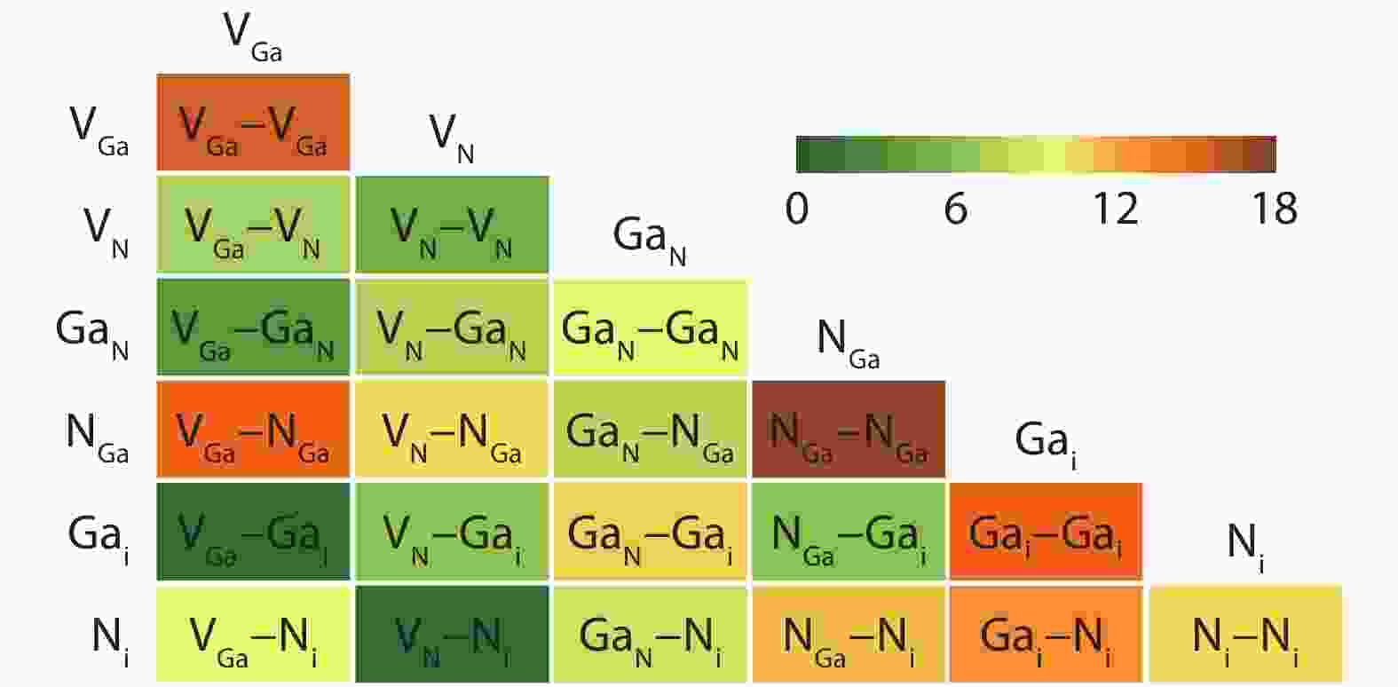
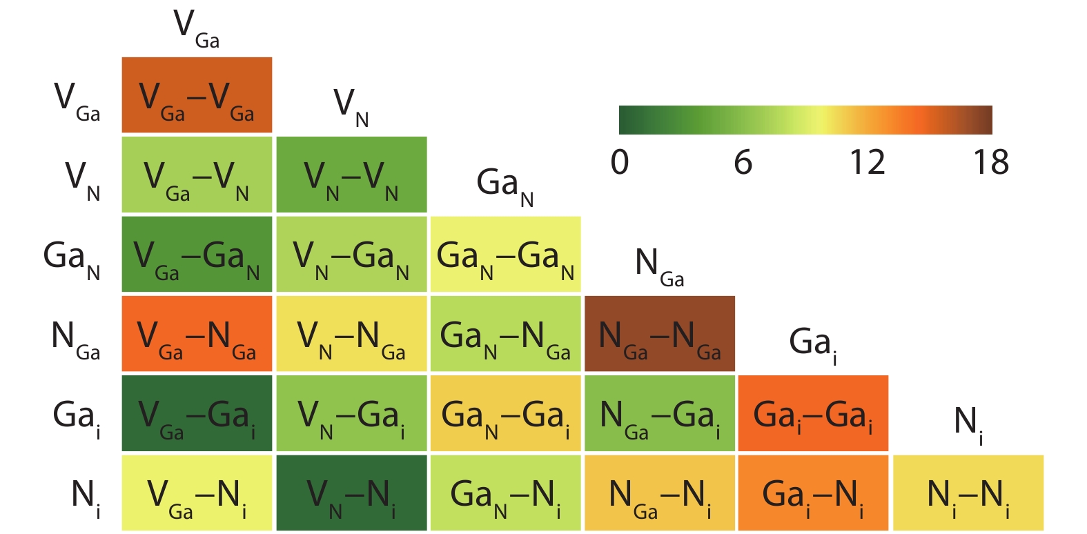
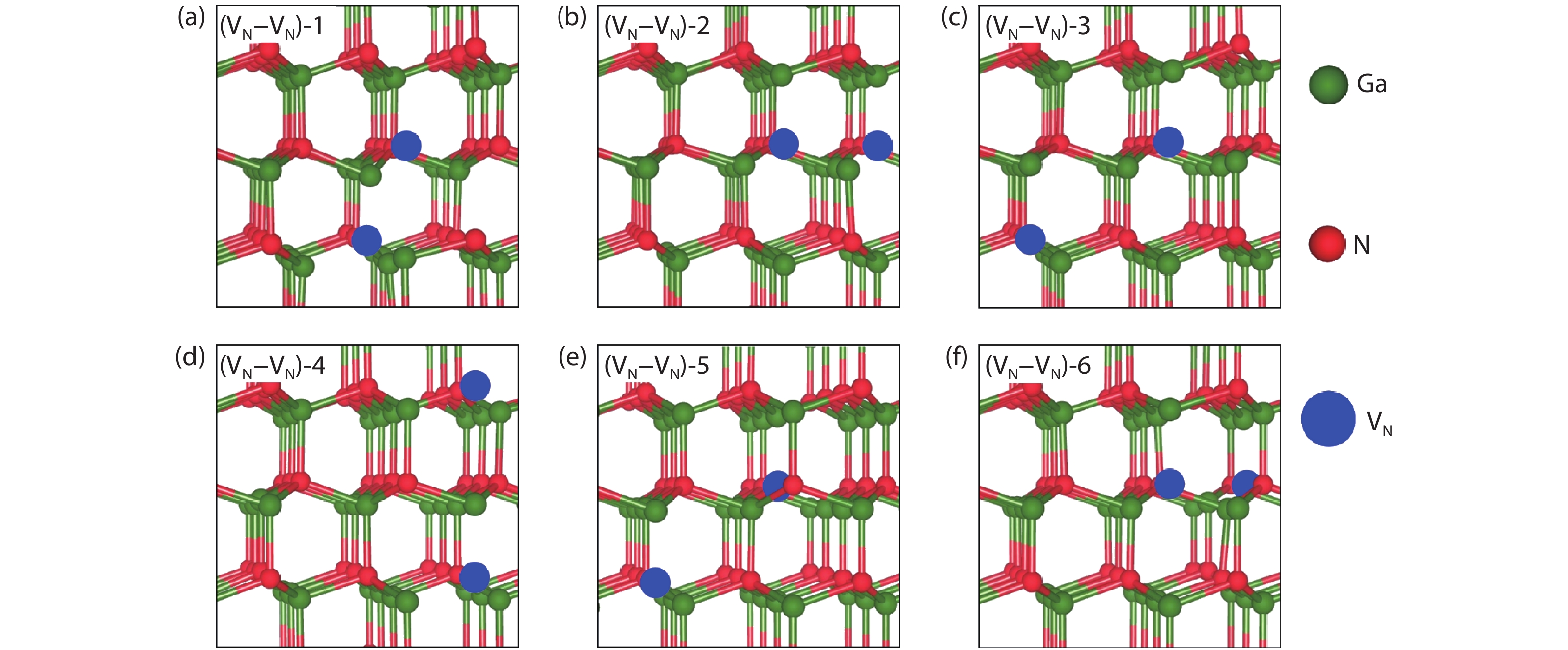
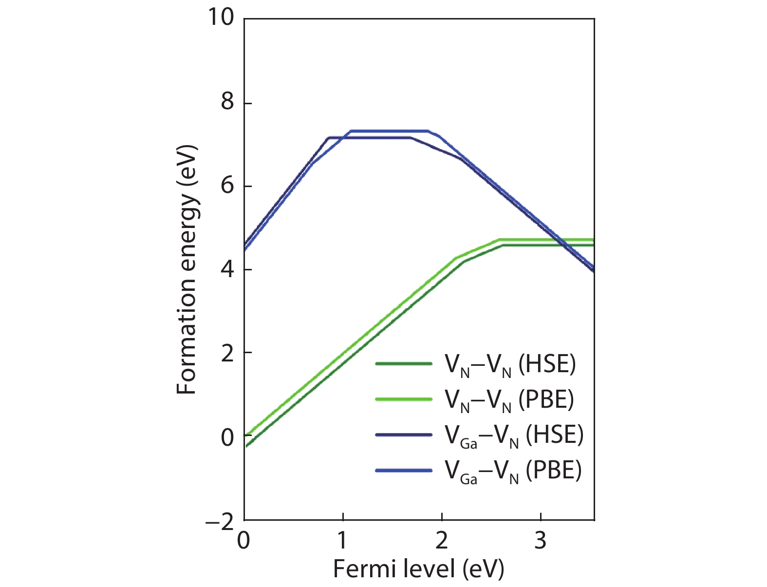
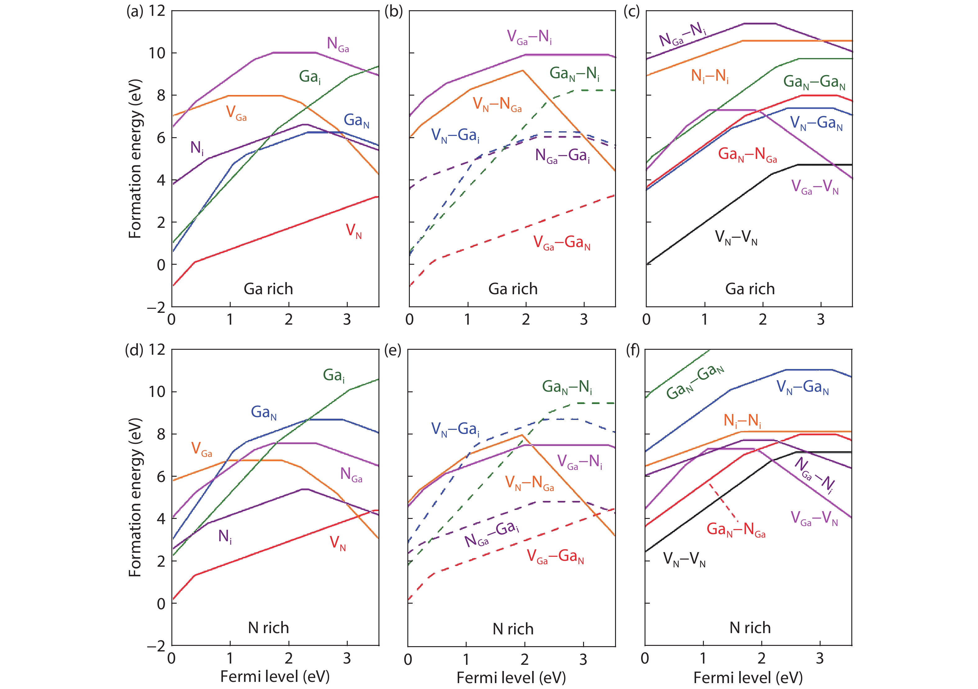
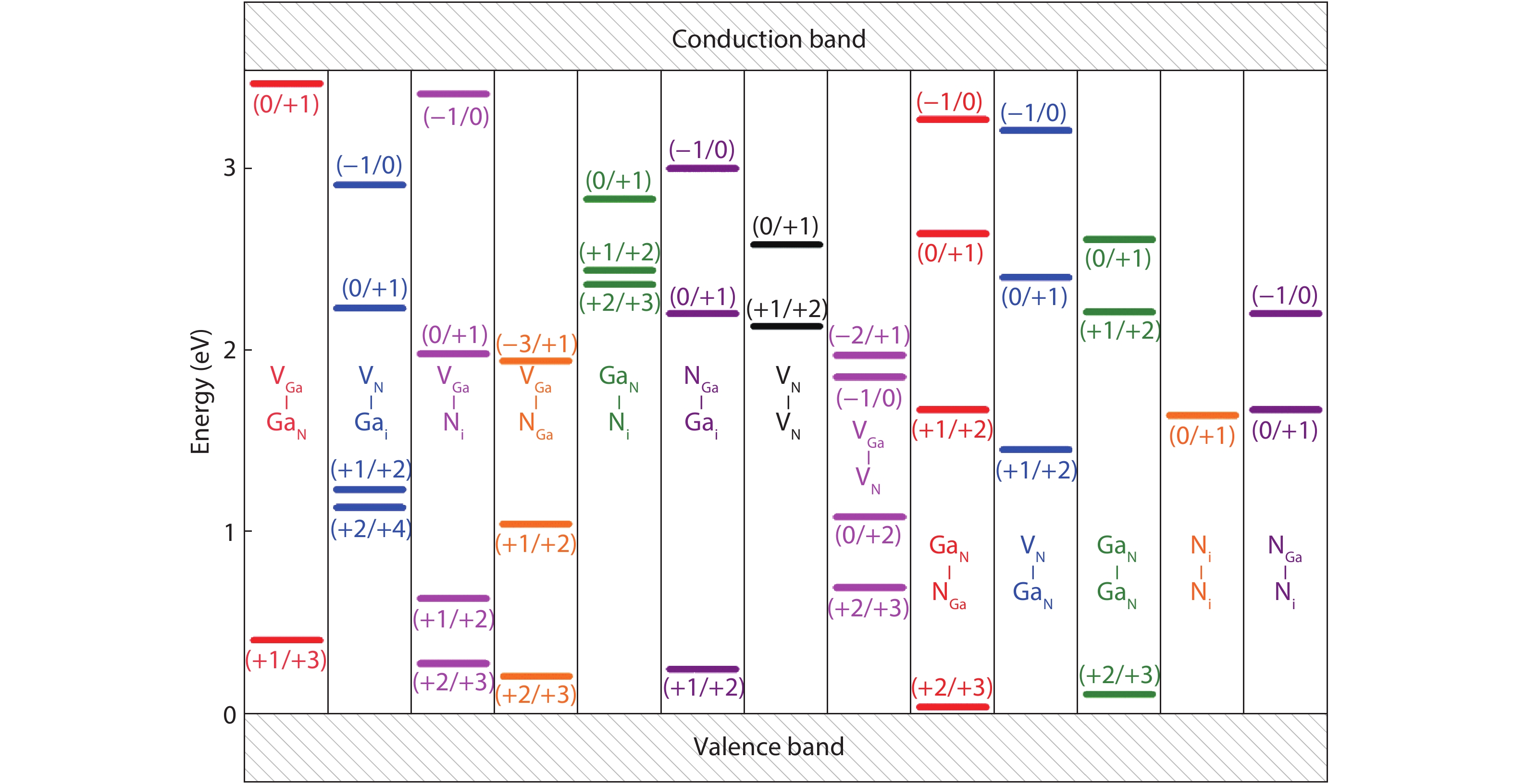
Using first-principles calculations, we explored all the 21 defect-pairs in GaN and considered 6 configurations with different defect-defect distances for each defect-pair. 15 defect-pairs with short defect–defect distances are found to be stable during structural relaxation, so they can exist in the GaN lattice once formed during the irradiation of high-energy particles. 9 defect-pairs have formation energies lower than 10 eV in the neutral state. The vacancy-pair VN–VN is found to have very low formation energies, as low as 0 eV in p-type and Ga-rich GaN, and act as efficient donors producing two deep donor levels, which can limit the p-type doping and minority carrier lifetime in GaN. VN–VN has been overlooked in the previous study of defects in GaN. Most of these defect-pairs act as donors and produce a large number of defect levels in the band gap. Their formation energies and concentrations are sensitive to the chemical potentials of Ga and N, so their influences on the electrical and optical properties of Ga-rich and N-rich GaN after irradiation should differ significantly. These results about the defect-pairs provide fundamental data for understanding the radiation damage mechanism in GaN and simulating the defect formation and diffusion behavior under irradiation.
J. Semicond.
2020, 41(3): 032301 doi: 10.1088/1674-4926/41/3/032301
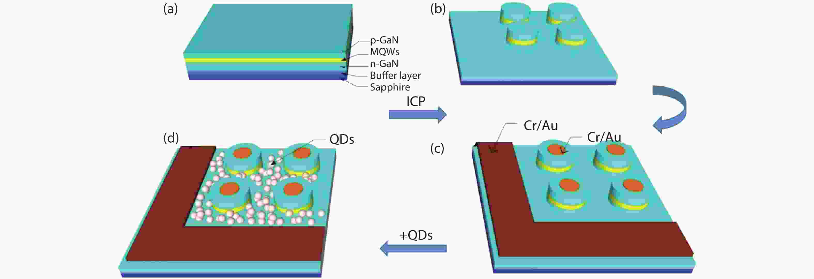
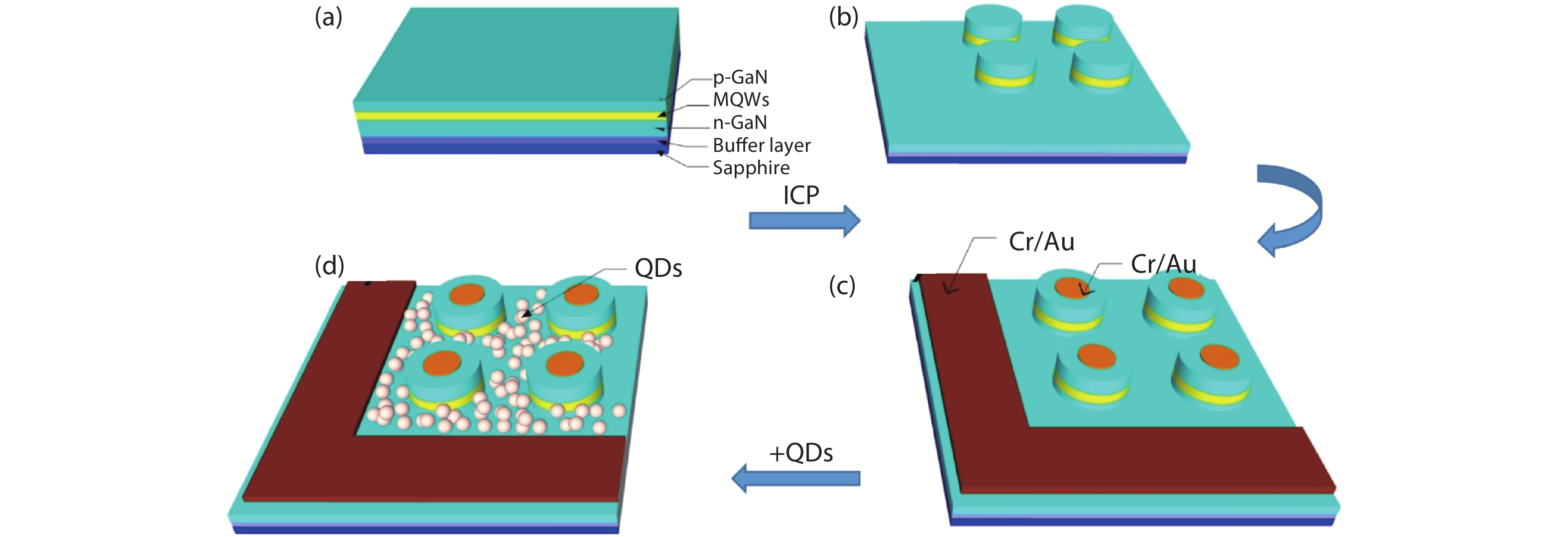
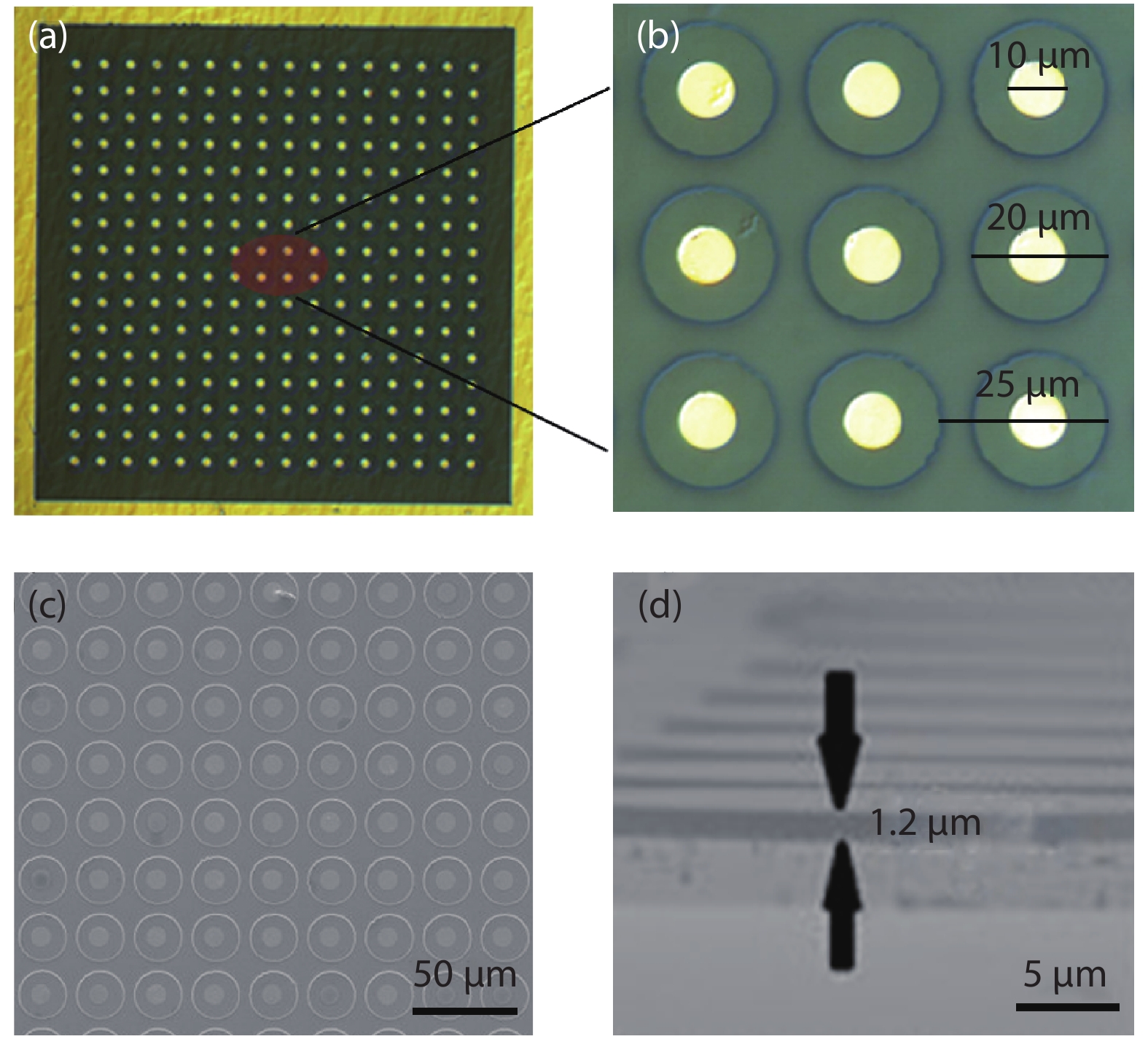
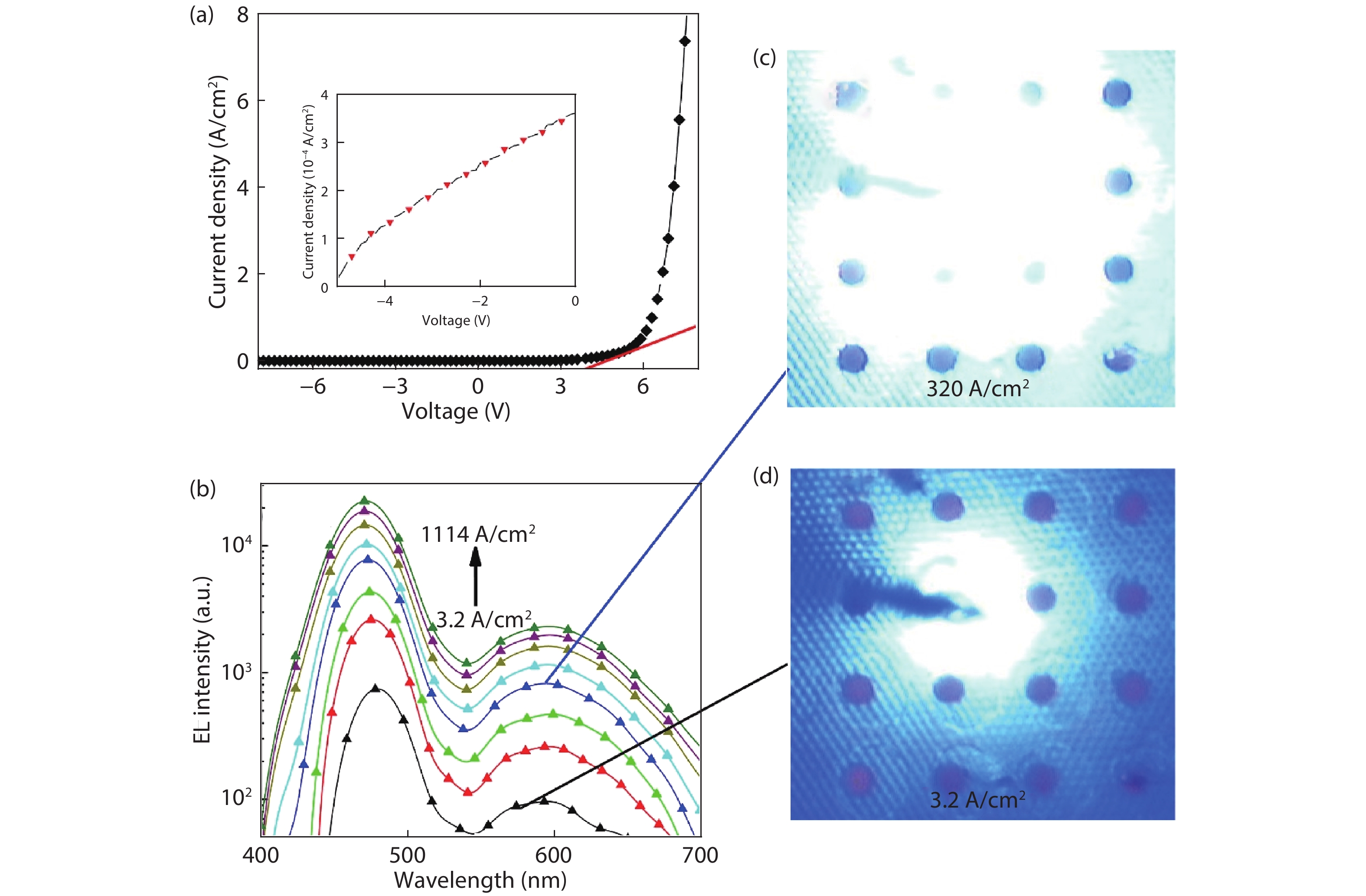
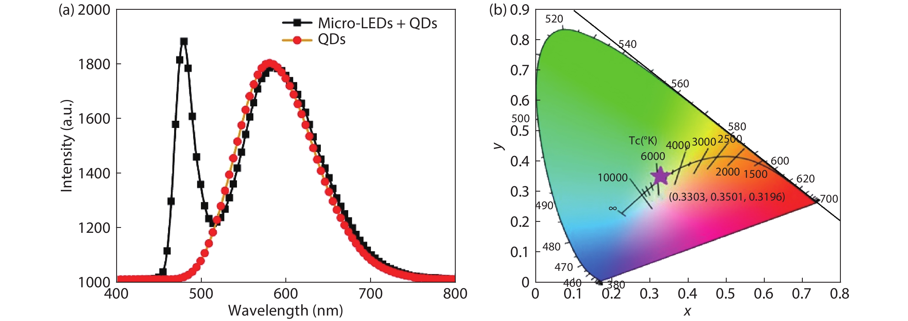
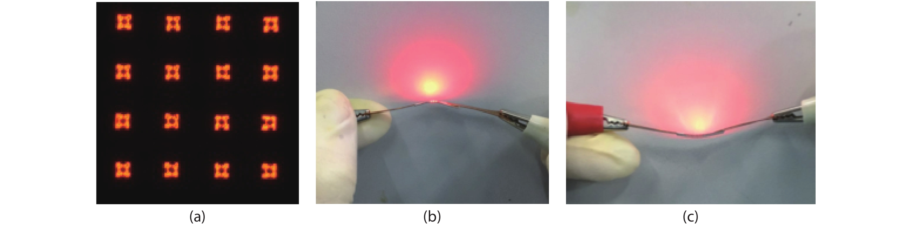
Hybrid white micro-pillar structure light emitting diodes (LEDs) have been manufacture utilizing blue micro-LEDs arrays integrated with 580 nm CIS ((CuInS2-ZnS)/ZnS) core/shell quantum dots. The fabricated hybrid white micro-LEDs have good electrical properties, which are manifested in relatively low turn-on voltage and reverse leakage current. High-quality hybrid white light emission has been demonstrated by the hybrid white micro-LEDs after a systemic optimization, in which the corresponding color coordinates are calculated to be (0.3303, 0.3501) and the calculated color temperature is 5596 K. This result indicates an effective way to achieve high-performance white LEDs and shows great promise in a large range of applications in the future including micro-displays, bioinstrumentation and visible light communication.
J. Semicond.
2020, 41(3): 032302 doi: 10.1088/1674-4926/41/3/032302
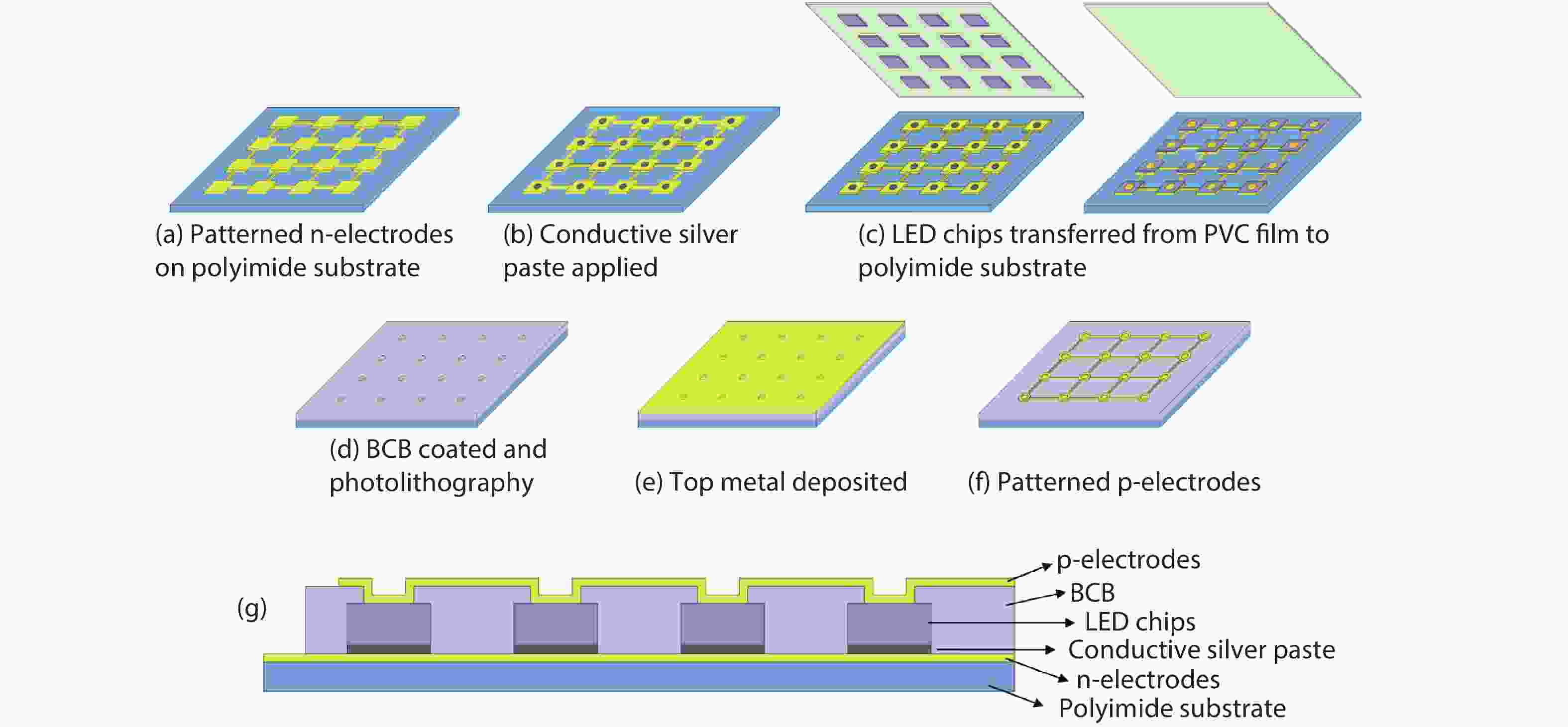
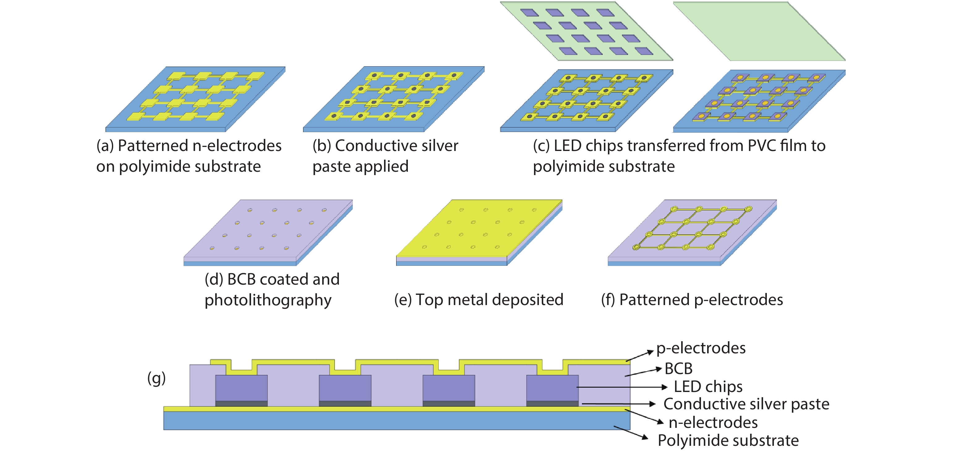
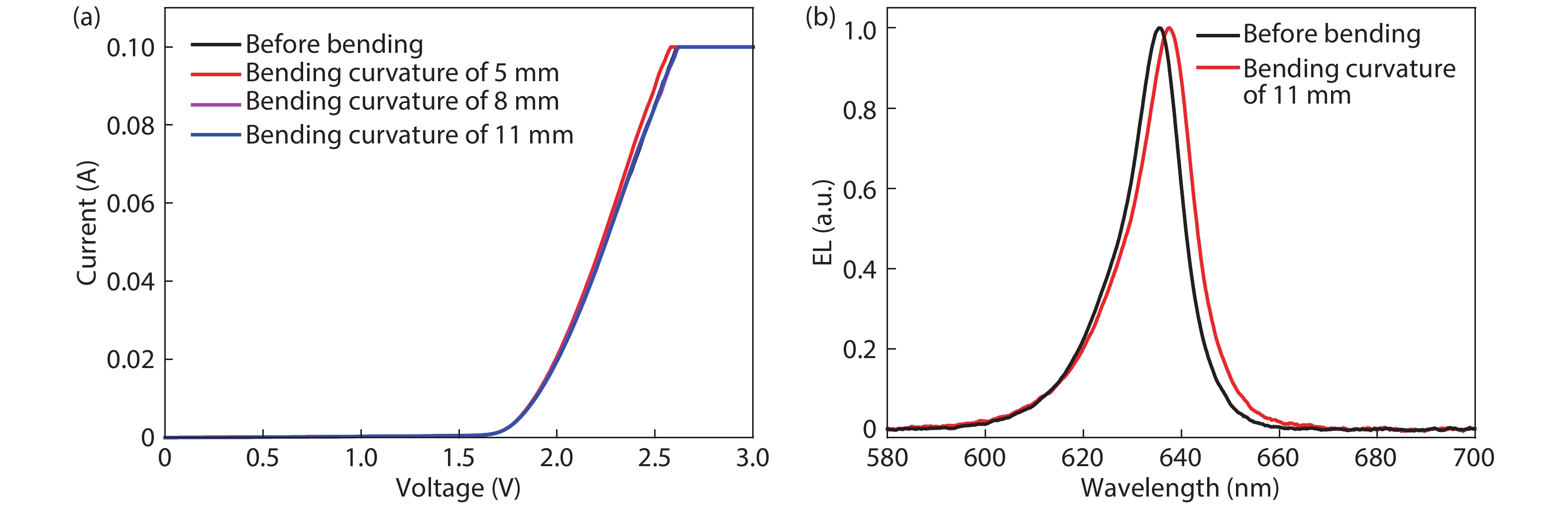
Flexible light-emitting diodes (LEDs) are highly desired for wearable devices, flexible displays, robotics, biomedicine, etc. Traditionally, the transfer process of an ultrathin wafer of about 10–30 μm to a flexible substrate is utilized. However, the yield is low, and it is not applicable to thick GaN LED chips with a 100 μm sapphire substrate. In this paper, transferable LED chips utilized the mature LED manufacture technique are developed, which possesses the advantage of high yield. The flexible LED array demonstrates good electrical and optical performance.
J. Semicond.
2020, 41(3): 032303 doi: 10.1088/1674-4926/41/3/032303

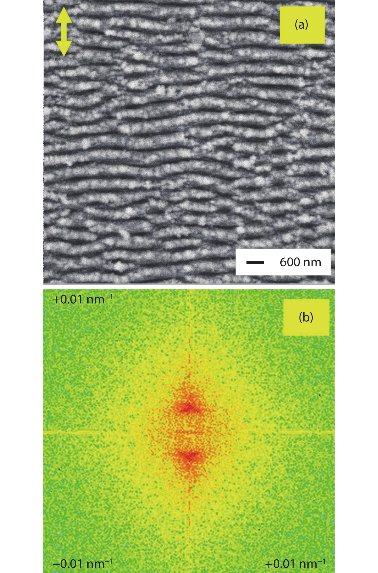
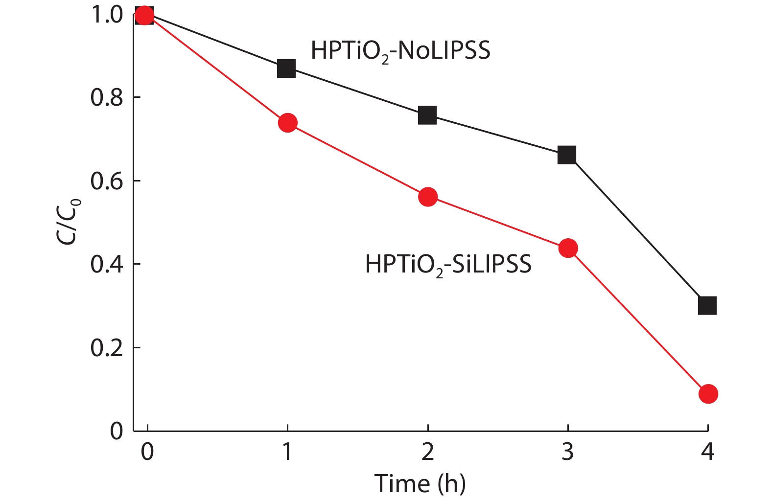
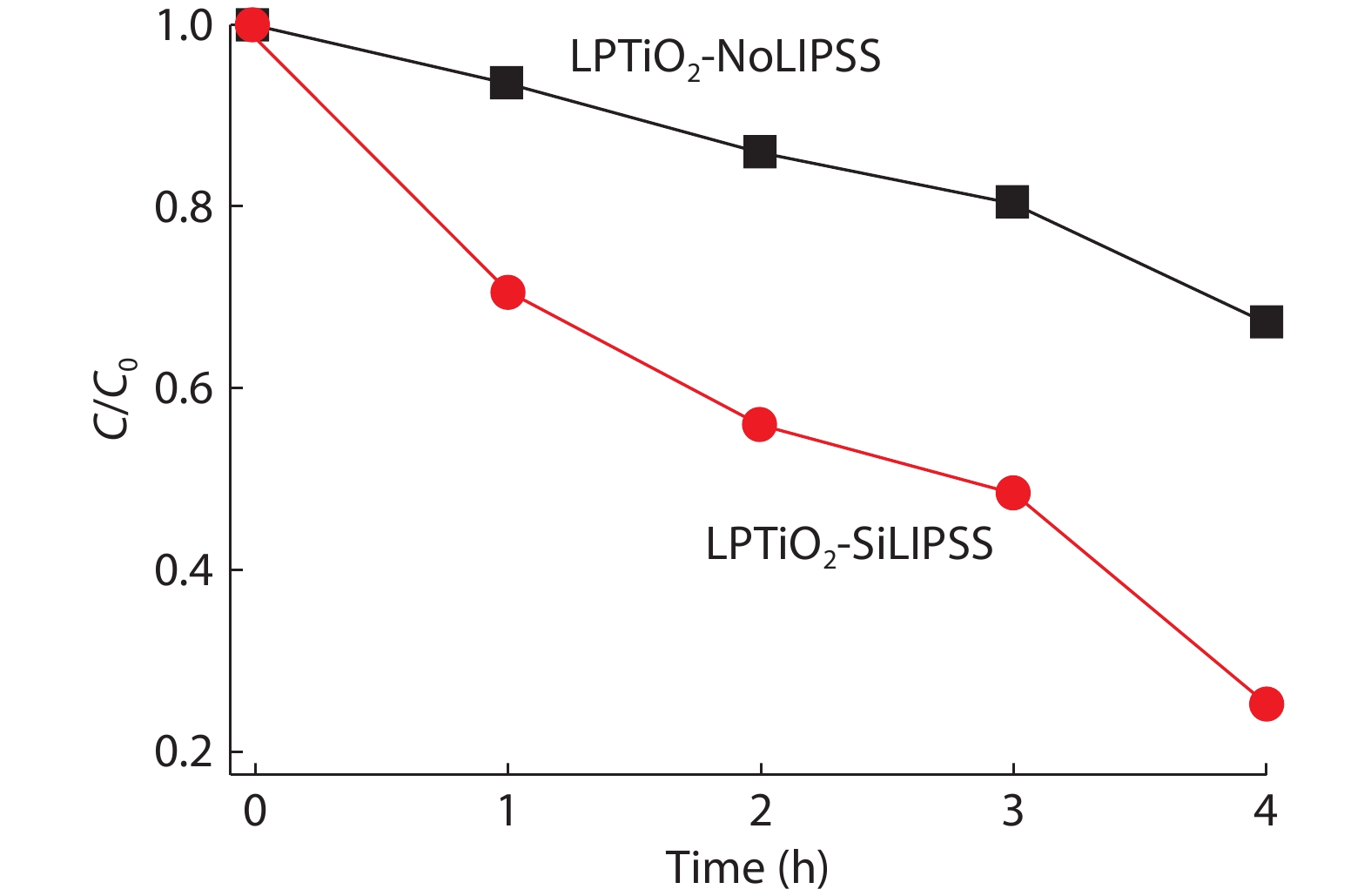
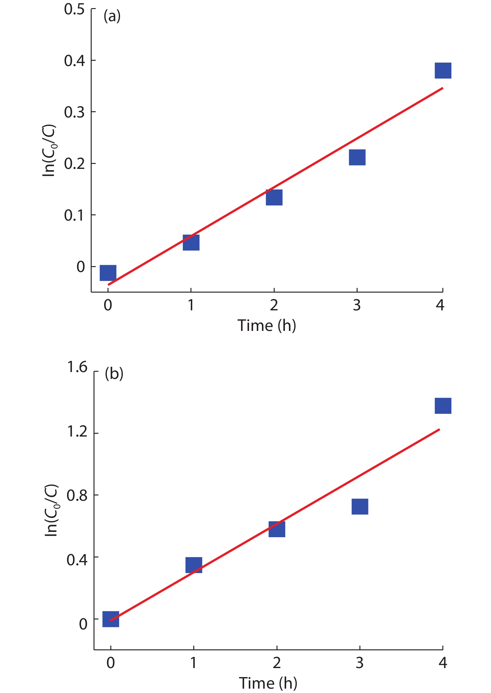
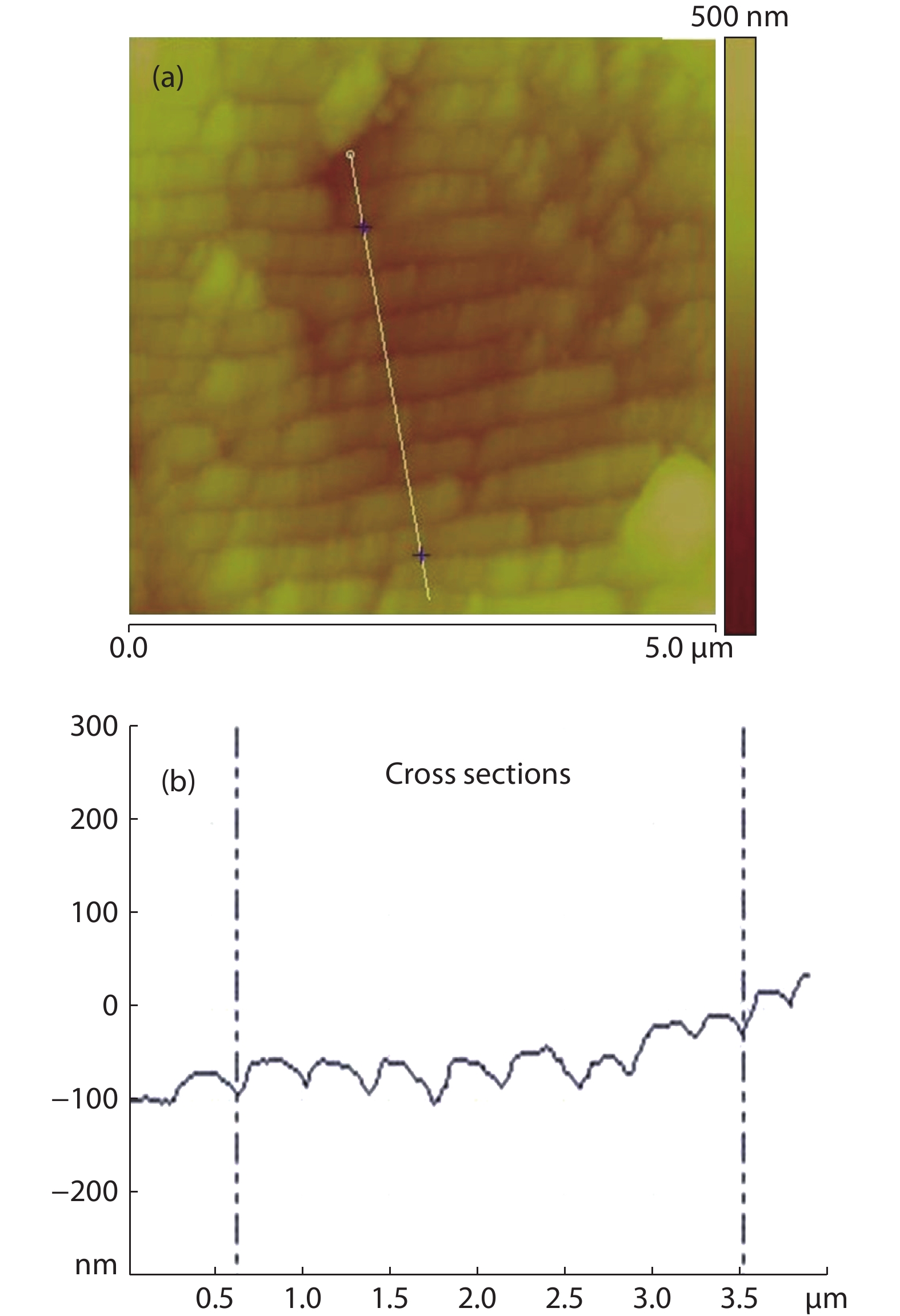
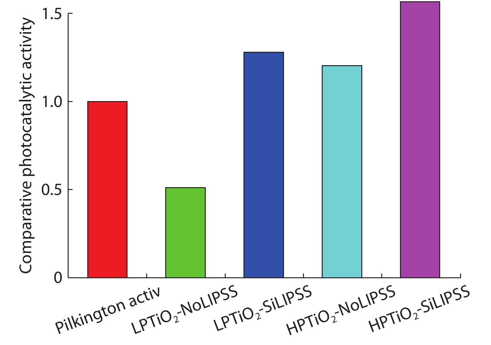
Laser induced periodic surface structures (LIPSS) represent a kind of top down approach to produce highly reproducible nano/microstructures without going for any sophisticated process of lithography. This method is much simpler and cost effective. In this work, LIPSS on Si surfaces were generated using femtosecond laser pulses of 800 nm wavelength. Photocatalytic substrates were prepared by depositing TiO2 thin films on top of the structured and unstructured Si wafer. The coatings were produced by sputtering from a Ti target in two different types of oxygen atmospheres. In first case, the oxygen pressure within the sputtering chamber was chosen to be high (3 × 10⁻² mbar) whereas it was one order of magnitude lower in second case (2.1 × 10⁻³ mbar). In photocatalytic dye decomposition study of Methylene blue dye it was found that in the presence of LIPSS the activity can be enhanced by 2.1 and 3.3 times with high pressure and low pressure grown TiO2 thin films, respectively. The increase in photocatalytic activity is attributed to the enlargement of effective surface area. In comparative study, the dye decomposition rates of TiO2 thin films grown on LIPSS are found to be much higher than the value for standard reference thin film material Pilkington ActivTM.

J. Semicond.
2020, 41(3): 032304 doi: 10.1088/1674-4926/41/3/032304
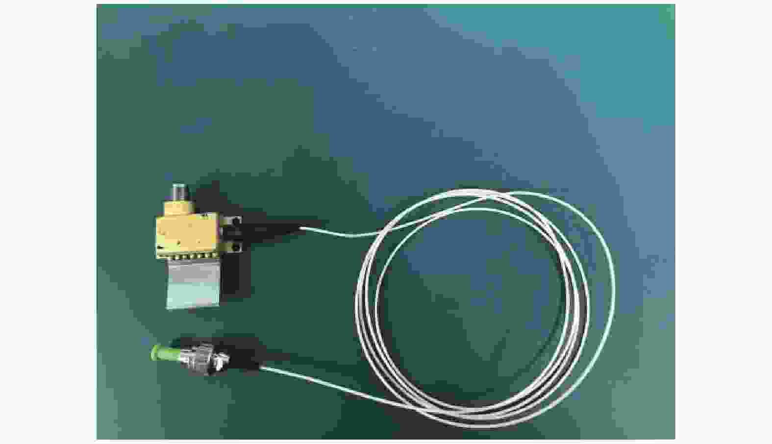
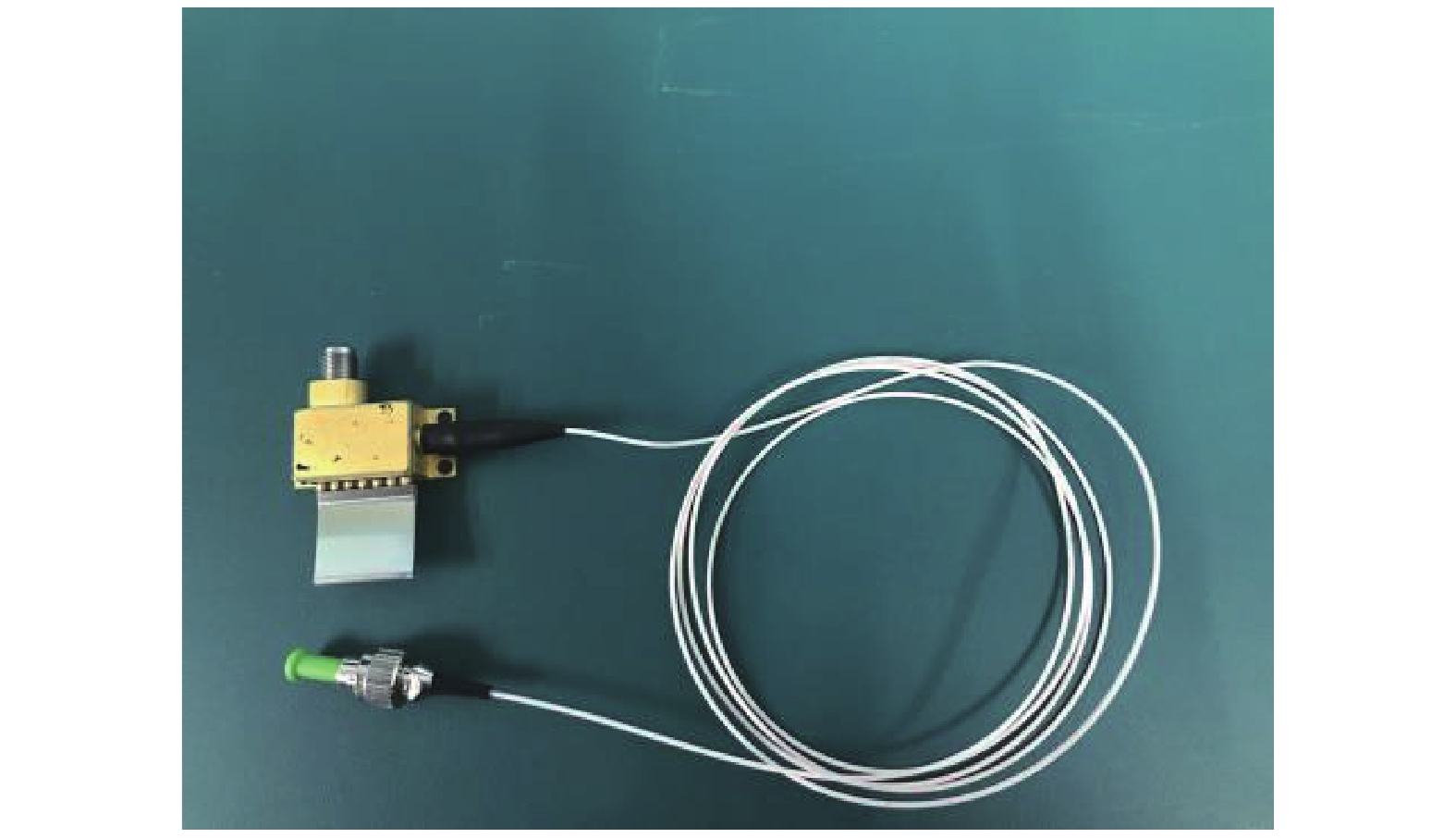
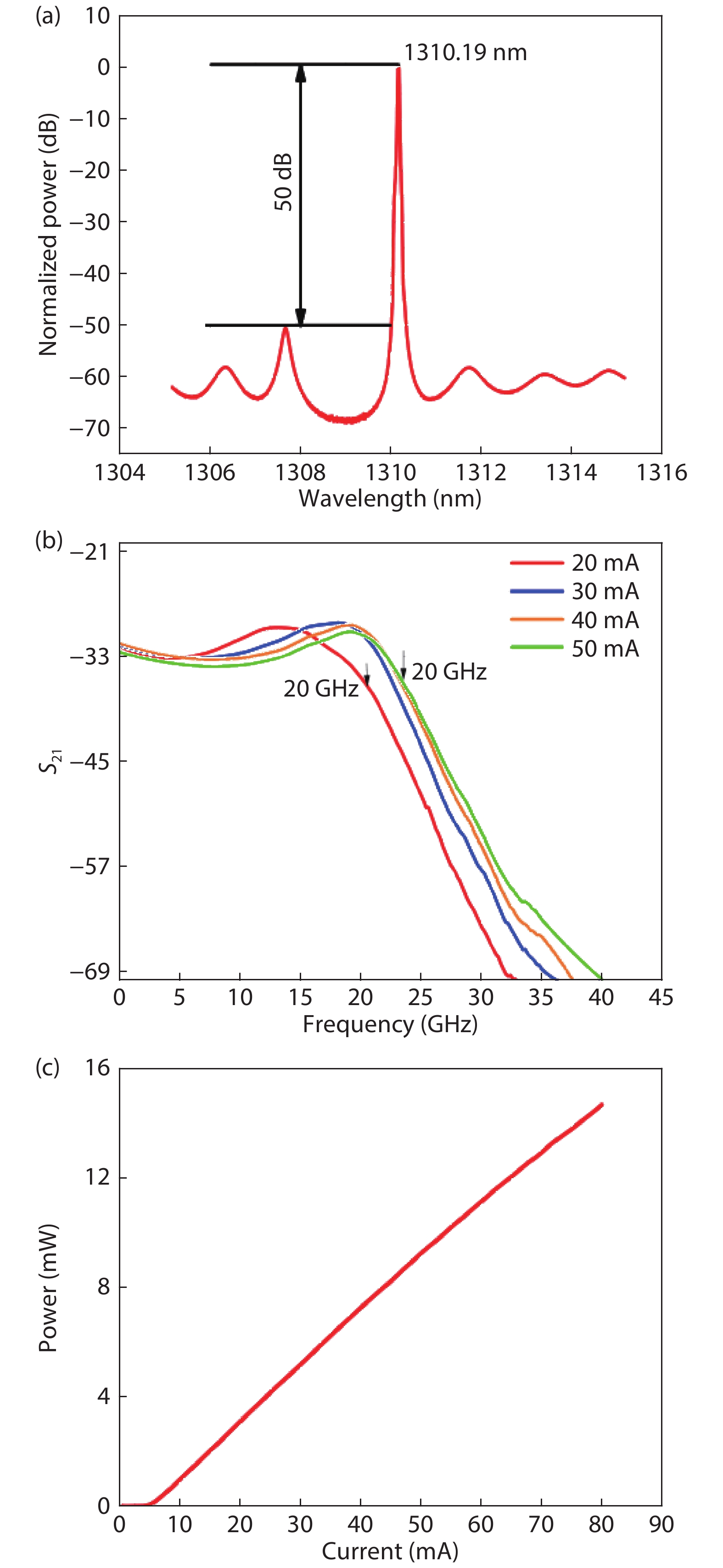
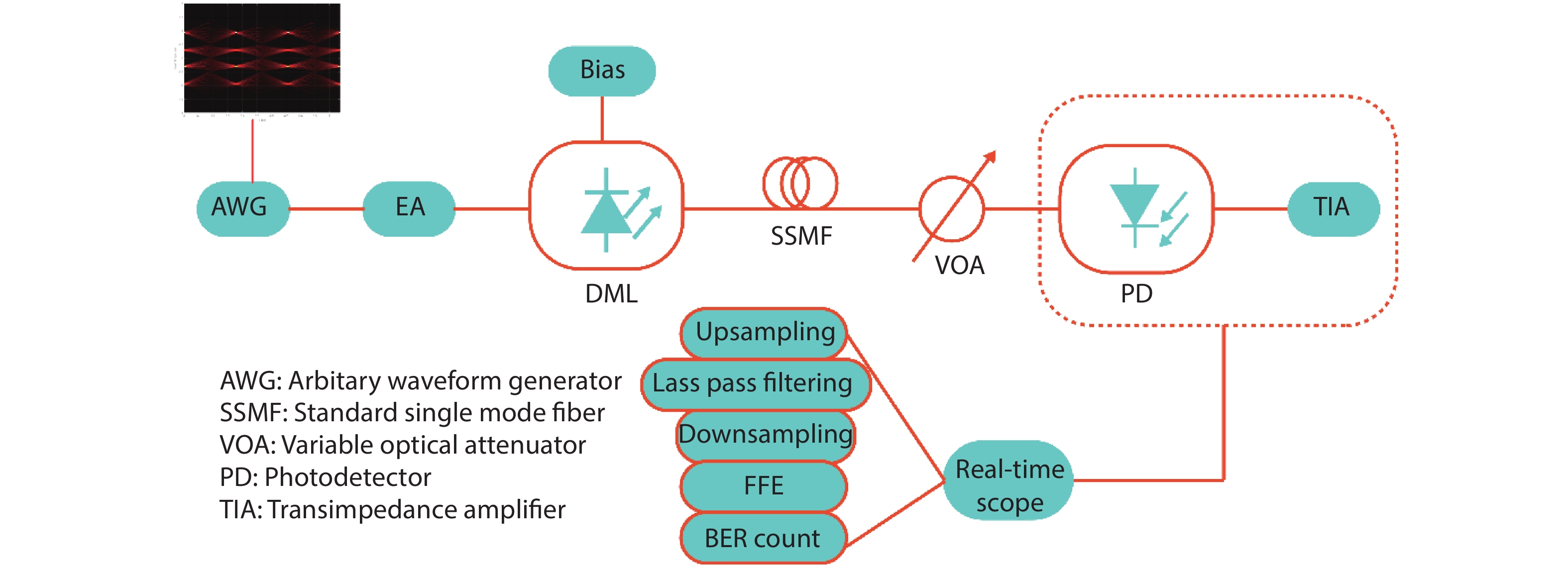
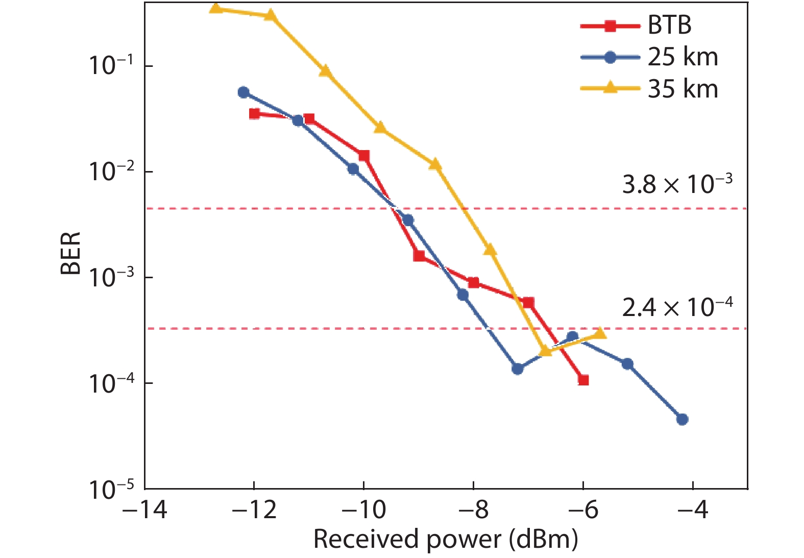
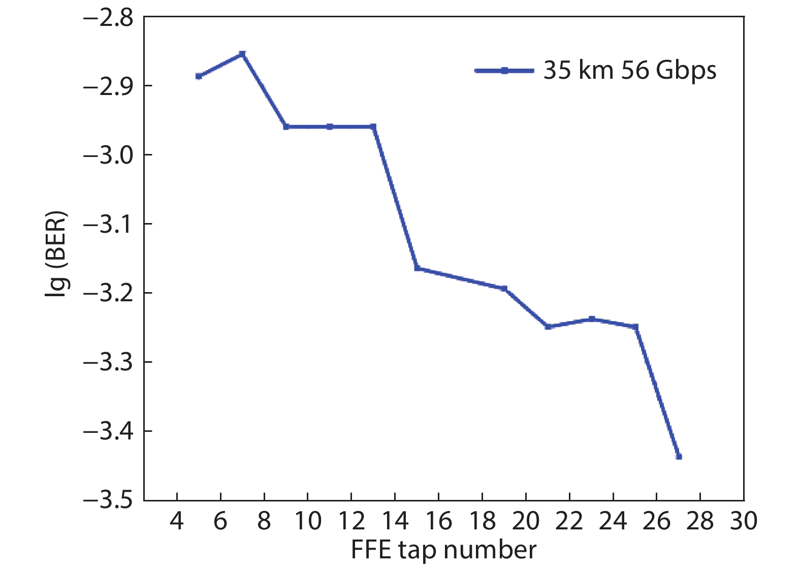
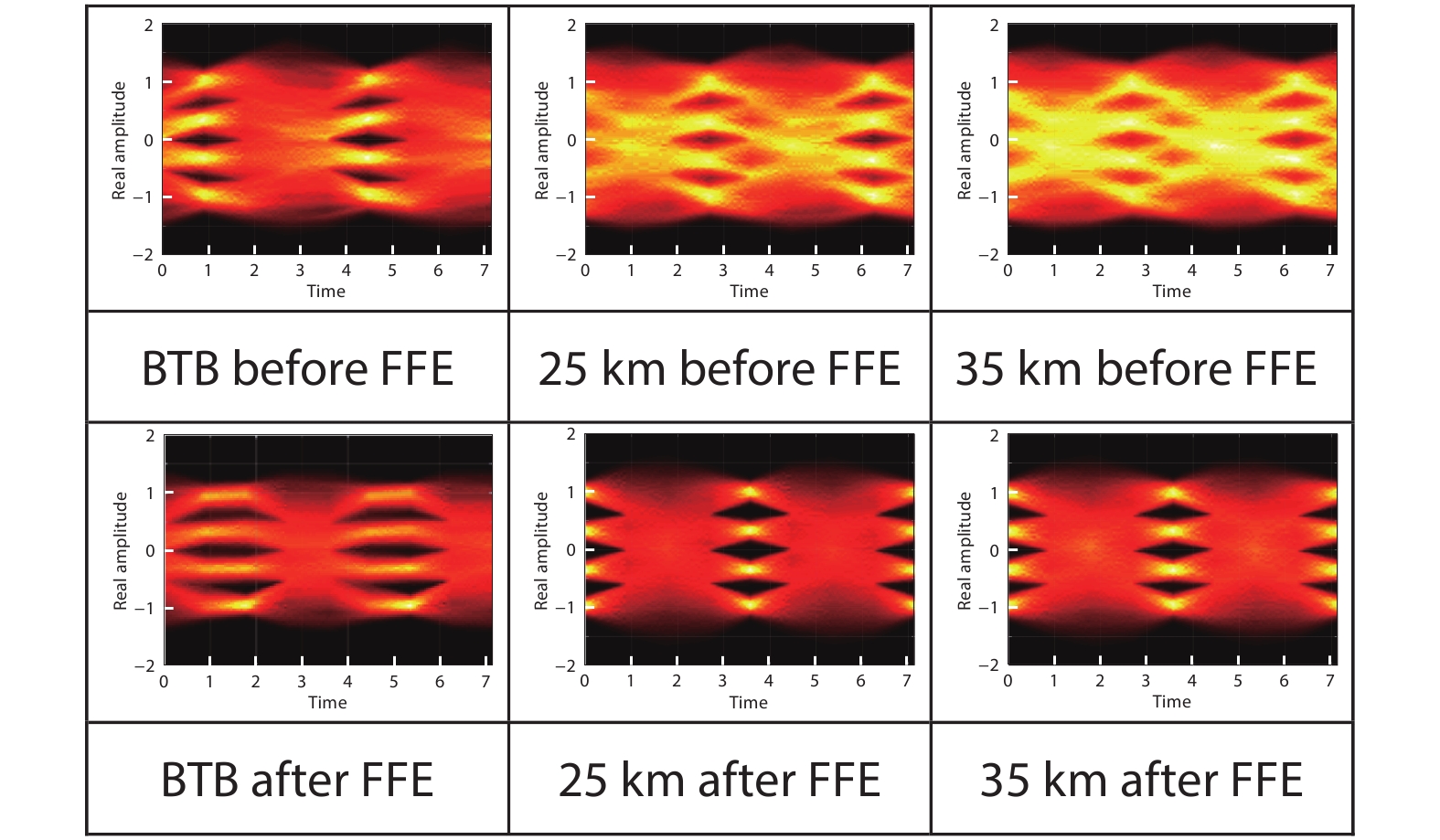
The 4-level pulse amplitude modulation (PAM4) based on an 23 GHz ultrabroadband directly modulated laser (DML) was proposed. We have experimentally demonstrated that based on intensity modulation and direct detection (IMDD) 56 Gbps per wavelength PAM4 signals transferred over 35 km standard single mode fiber (SSMF) without any optical amplification and we have achieved the bit error rate (BER) of the PAM4 transmission was under 2.9 × 10⁻⁴ by using feed forward equalization (FFE).

J. Semicond.
2020, 41(3): 032305 doi: 10.1088/1674-4926/41/3/032305

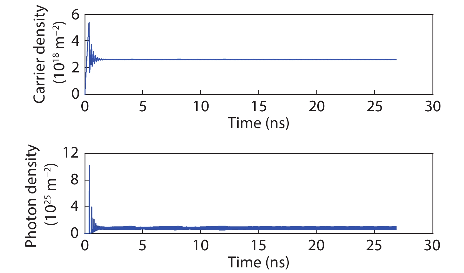
We use traveling wave coupling theory to investigate the time domain characteristics of tapered semiconductor lasers with DBR gratings. We analyze the influence of the length of second order gratings on the power and spectrum of output light, and optimizing the length of gratings, in order to reduce the mode competition effect in the device, and obtain the high power output light wave with good longitudinal mode characteristics.


J. Semicond.
2020, 41(3): 032701 doi: 10.1088/1674-4926/41/3/032701

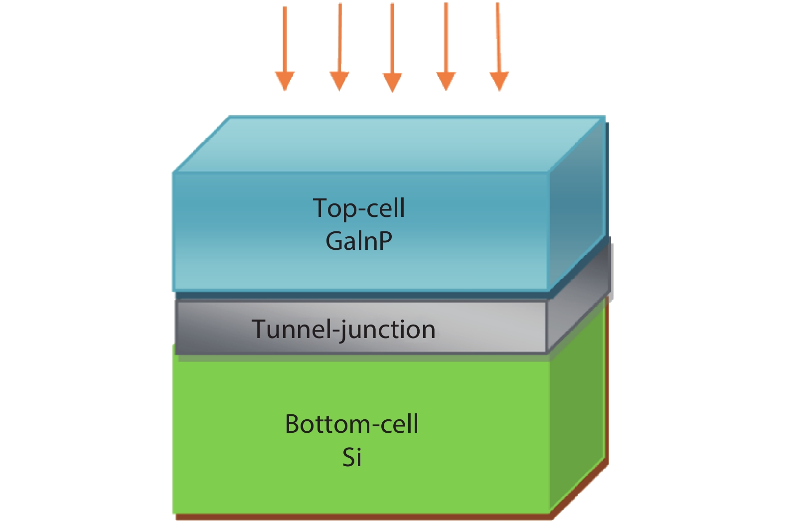
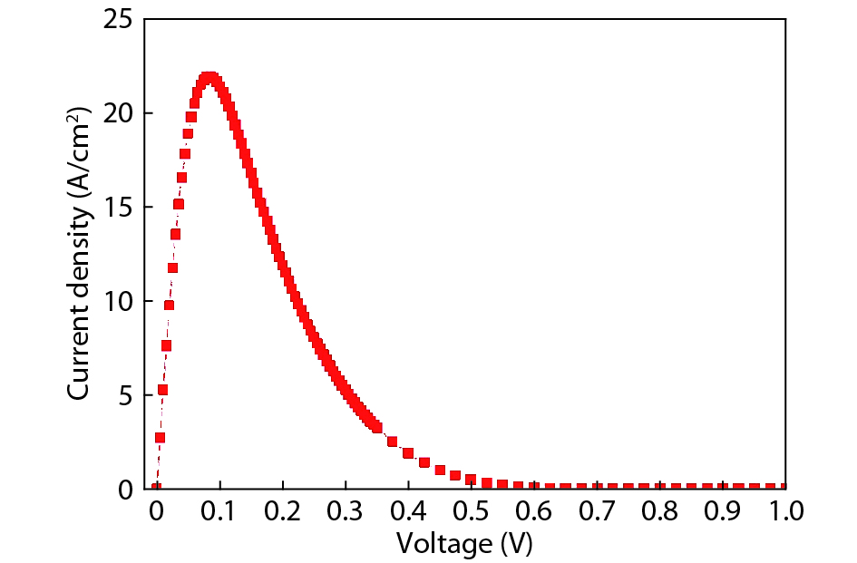
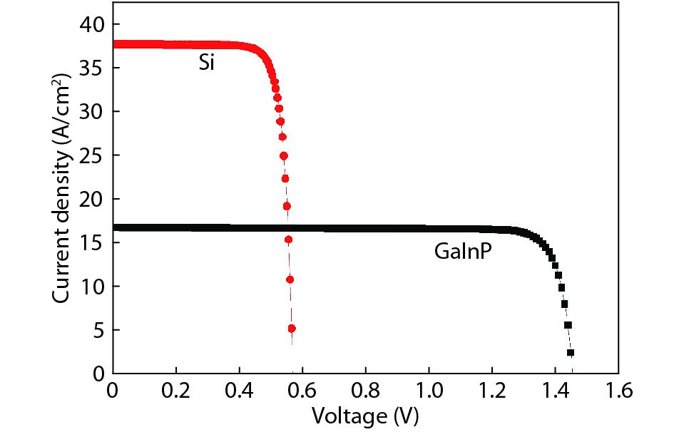
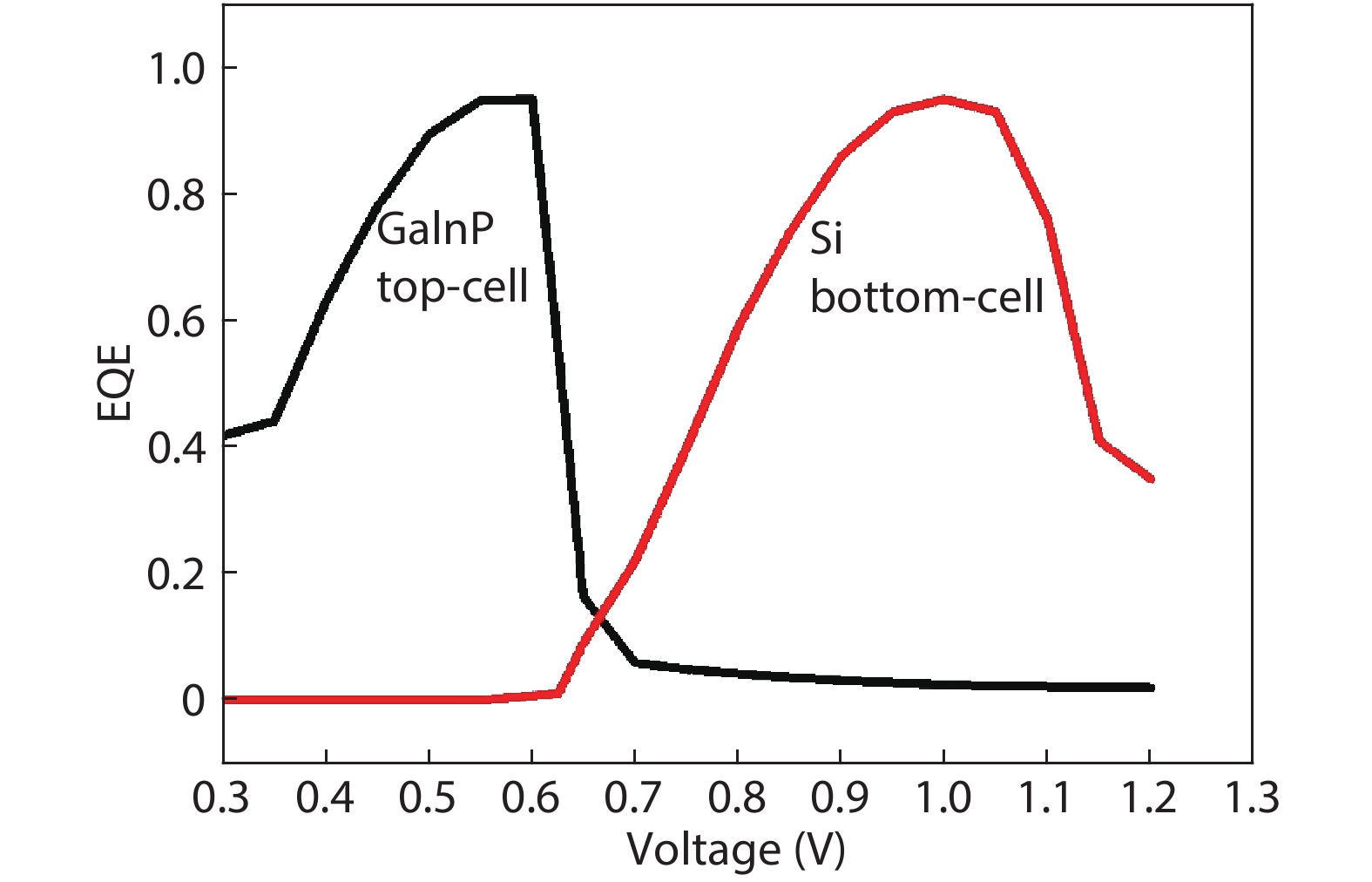
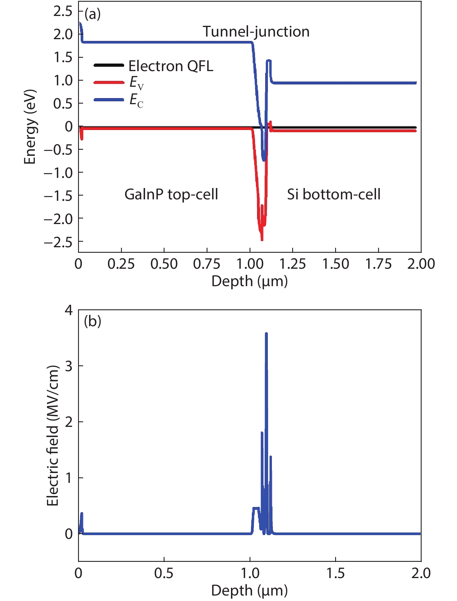
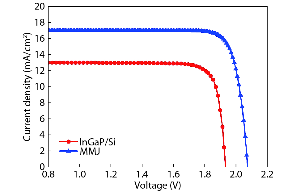
The solar power conversion efficiency of a gallium indium phosphide (GaInP)/silicon (Si) tandem solar cell has been investigated by means of a physical device simulator considering both mechanically stacked and monolithic structures. In particular, to interconnect the bottom and top sub-cells of the monolithic tandem, a gallium arsenide (GaAs)-based tunnel-junction, i.e. GaAs(n+)/GaAs(p+), which assures a low electrical resistance and an optically low-loss connection, has been considered. The J–V characteristics of the single junction cells, monolithic tandem, and mechanically stacked structure have been calculated extracting the main photovoltaic parameters. An analysis of the tunnel-junction behaviour has been also developed. The mechanically stacked cell achieves an efficiency of 24.27% whereas the monolithic tandem reaches an efficiency of 31.11% under AM1.5 spectral conditions. External quantum efficiency simulations have evaluated the useful wavelength range. The results and discussion could be helpful in designing high efficiency monolithic multijunction GaInP/Si solar cells involving a thin GaAs(n+)/GaAs(p+) tunnel junction.

J. Semicond.
2020, 41(3): 032901 doi: 10.1088/1674-4926/41/3/032901
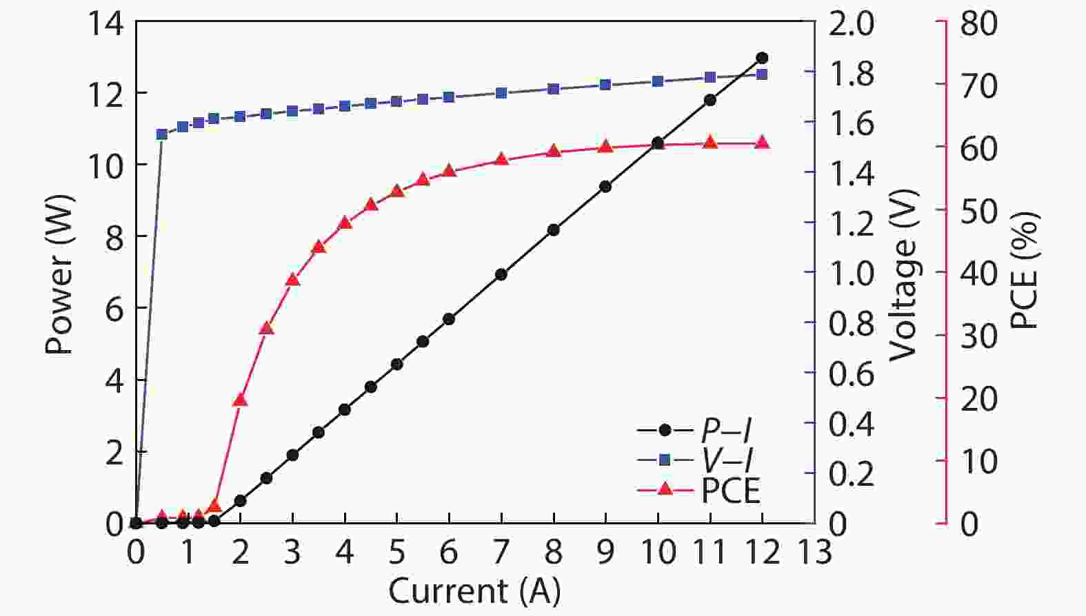
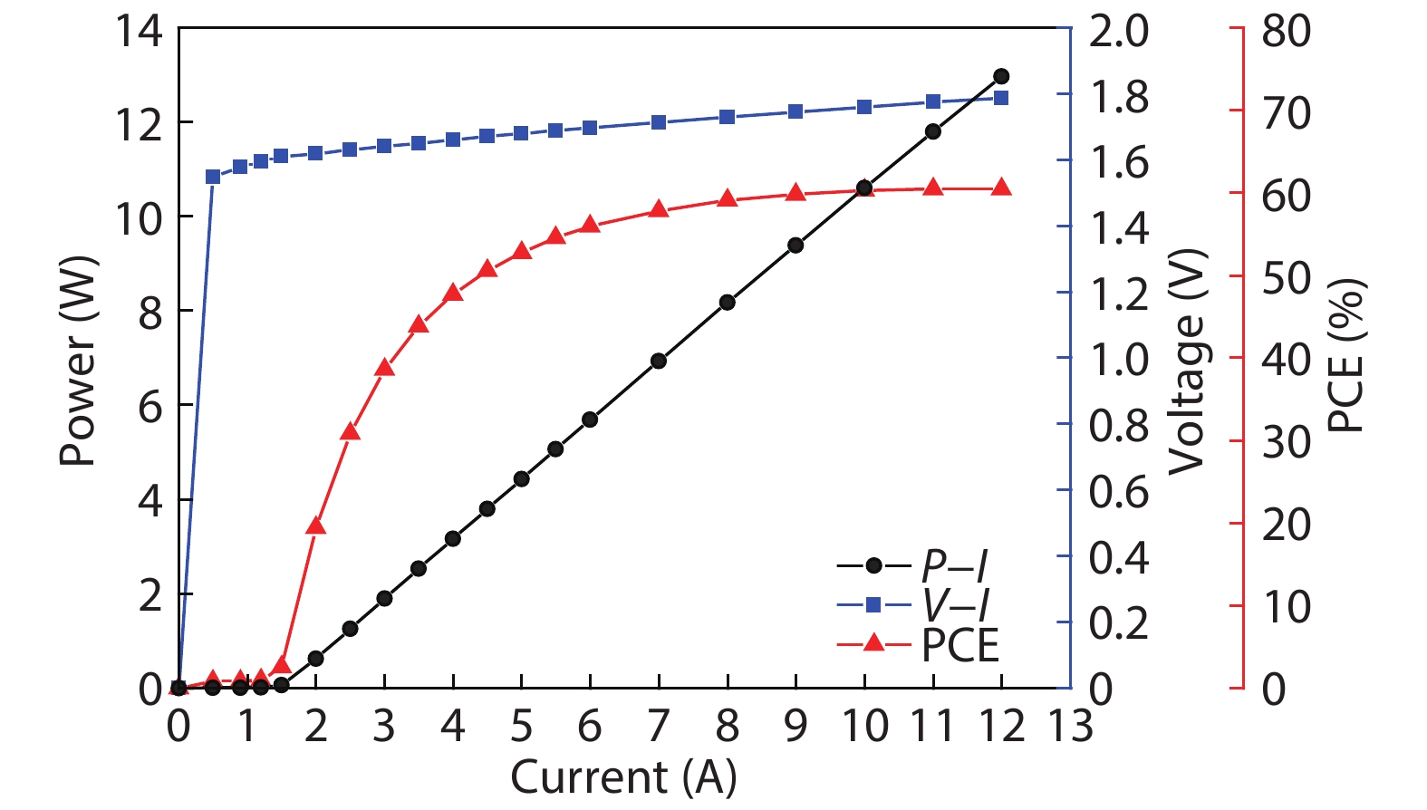
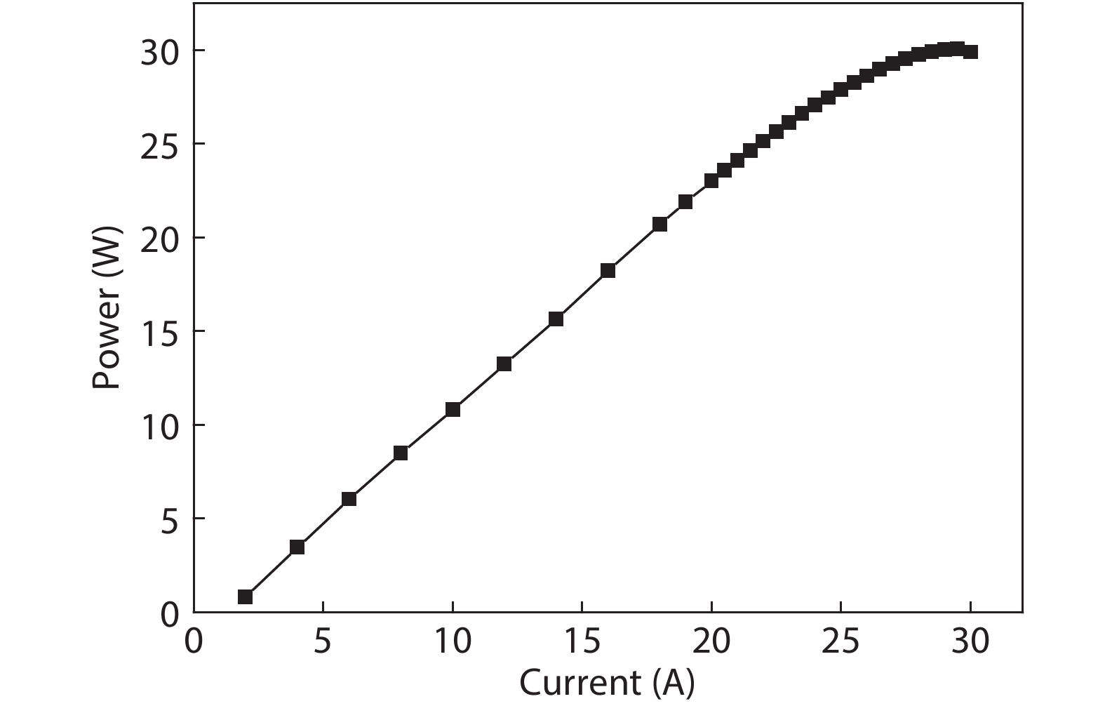
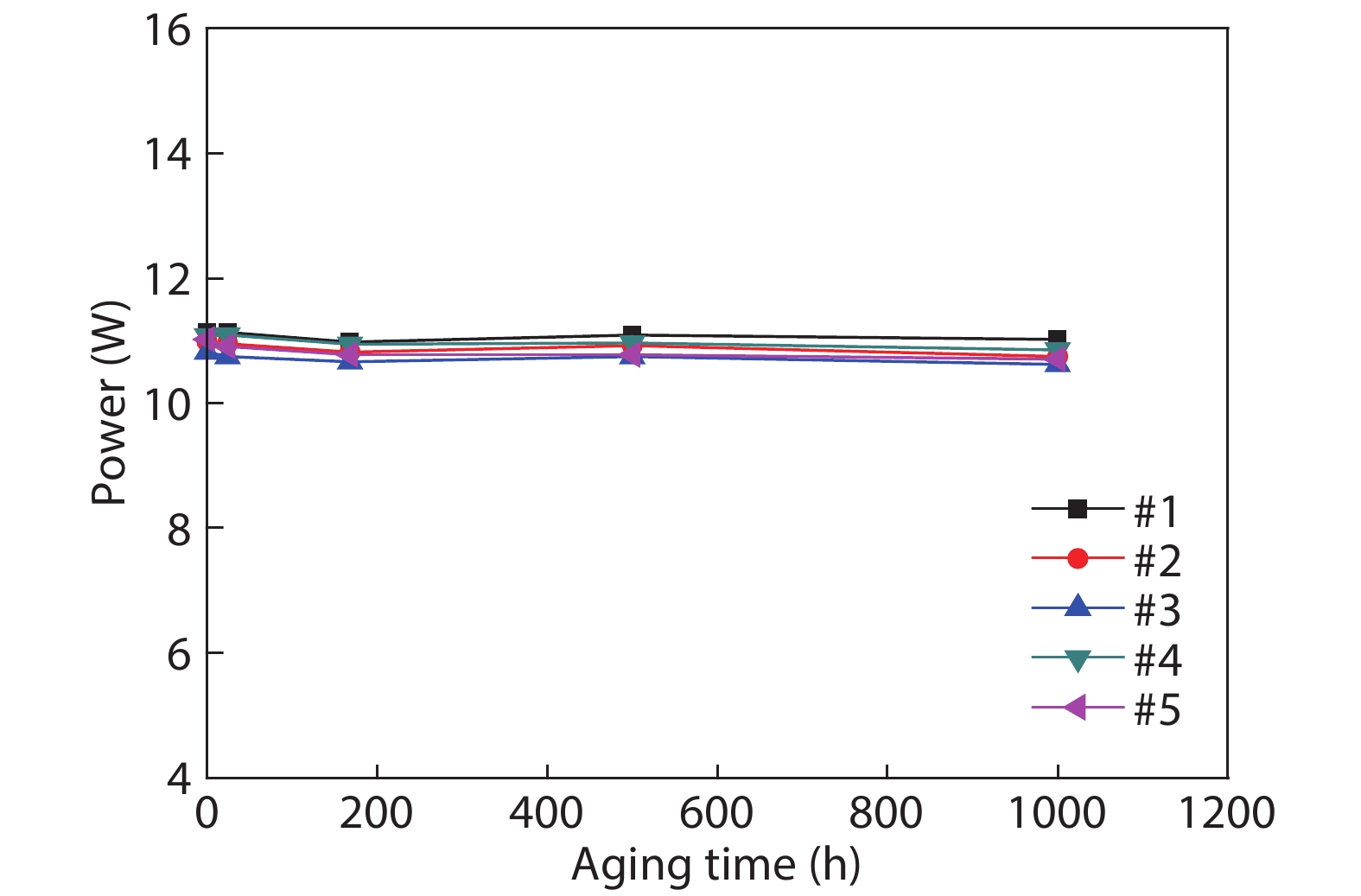
A very highly efficient InGaAlAs/AlGaAs quantum-well structure was designed for 808 nm emission, and laser diode chips 390-μm-wide aperture and 2-mm-long cavity length were fabricated. Special pretreatment and passivation for the chip facets were performed to achieve improved reliability performance. The laser chips were p-side-down mounted on the AlN sub-mount, and then tested at continuous wave (CW) operation with the heat-sink temperature setting to 25 °C using a thermoelectric cooler (TEC). As high as 60.5% of the wall-plug efficiency (WPE) was achieved at the injection current of 11 A. The maximum output power of 30.1 W was obtained at 29.5 A when the TEC temperature was set to 12 °C. Accelerated life-time test showed that the laser diodes had lifetimes of over 62 111 h operating at rated power of 10 W.