Issue Browser
Volume 41, Issue 8,
Aug 2020

J. Semicond.
2020, 41(8): 081001 doi: 10.1088/1674-4926/41/8/081001
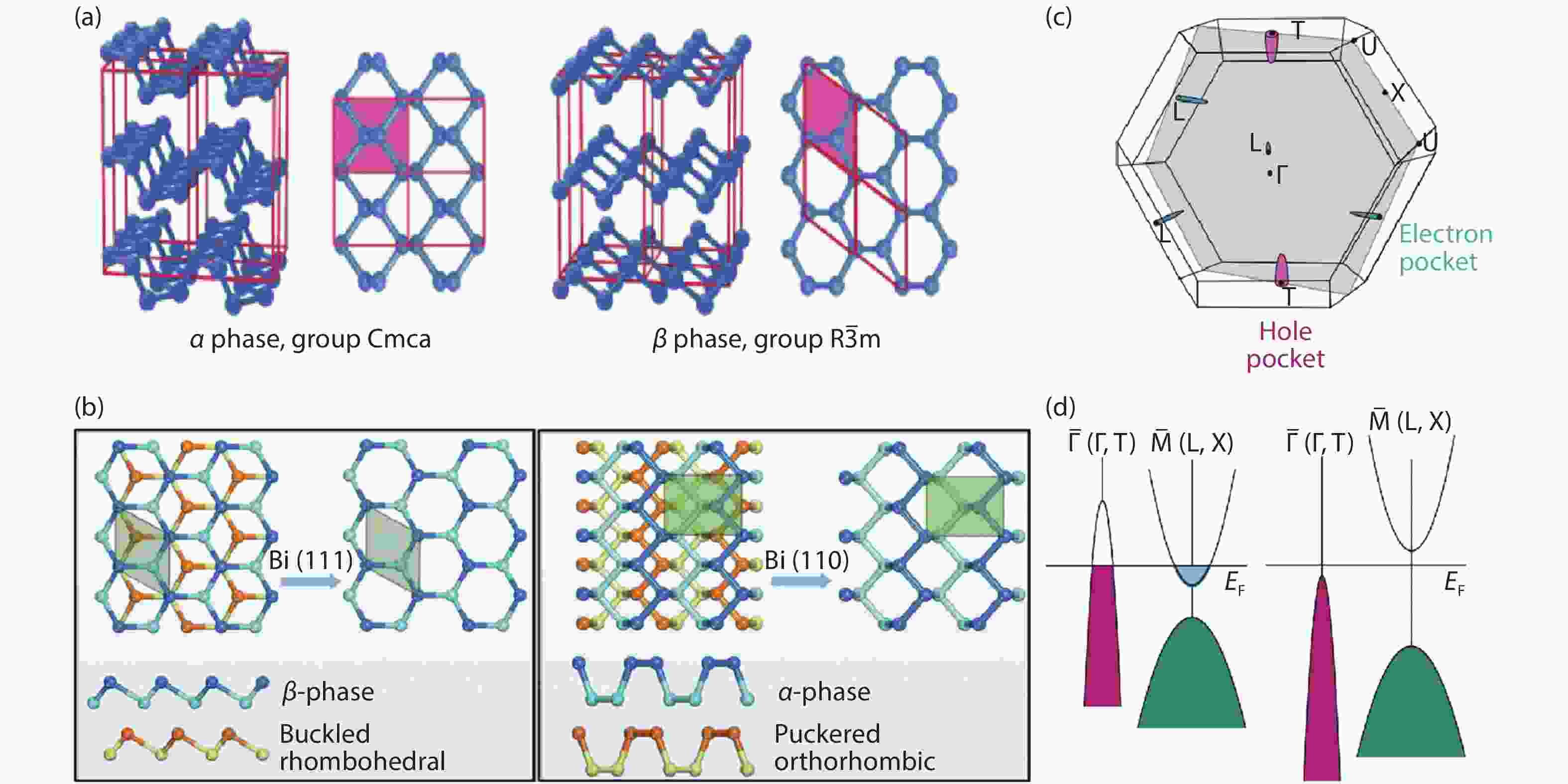
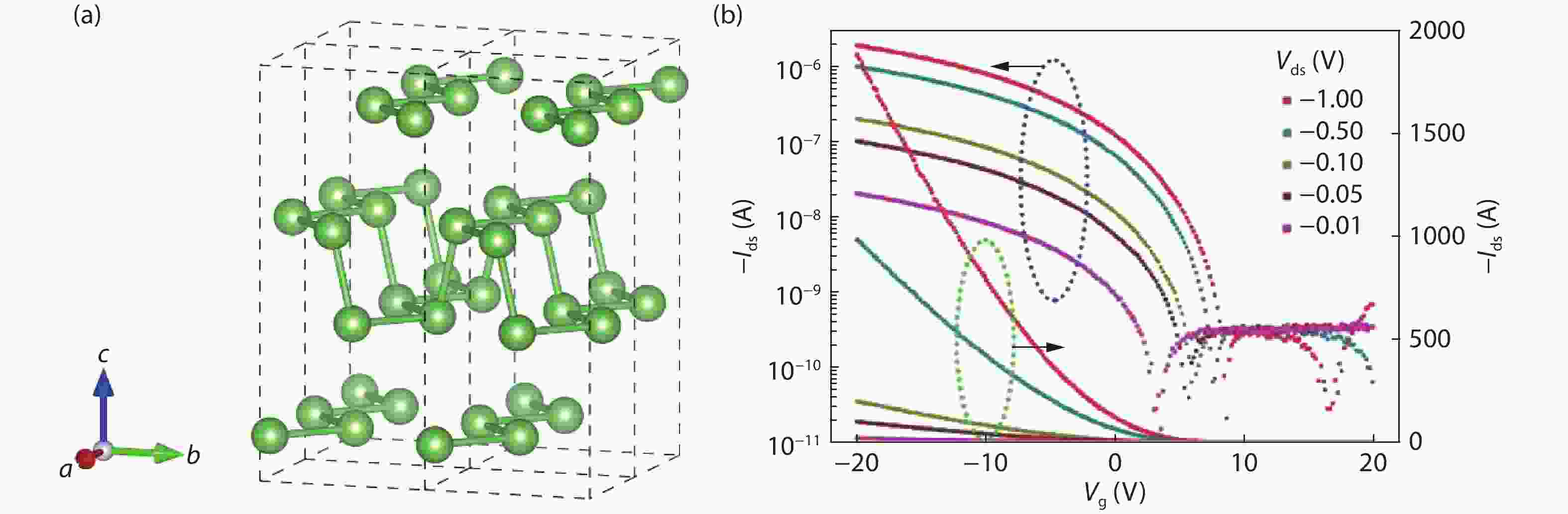
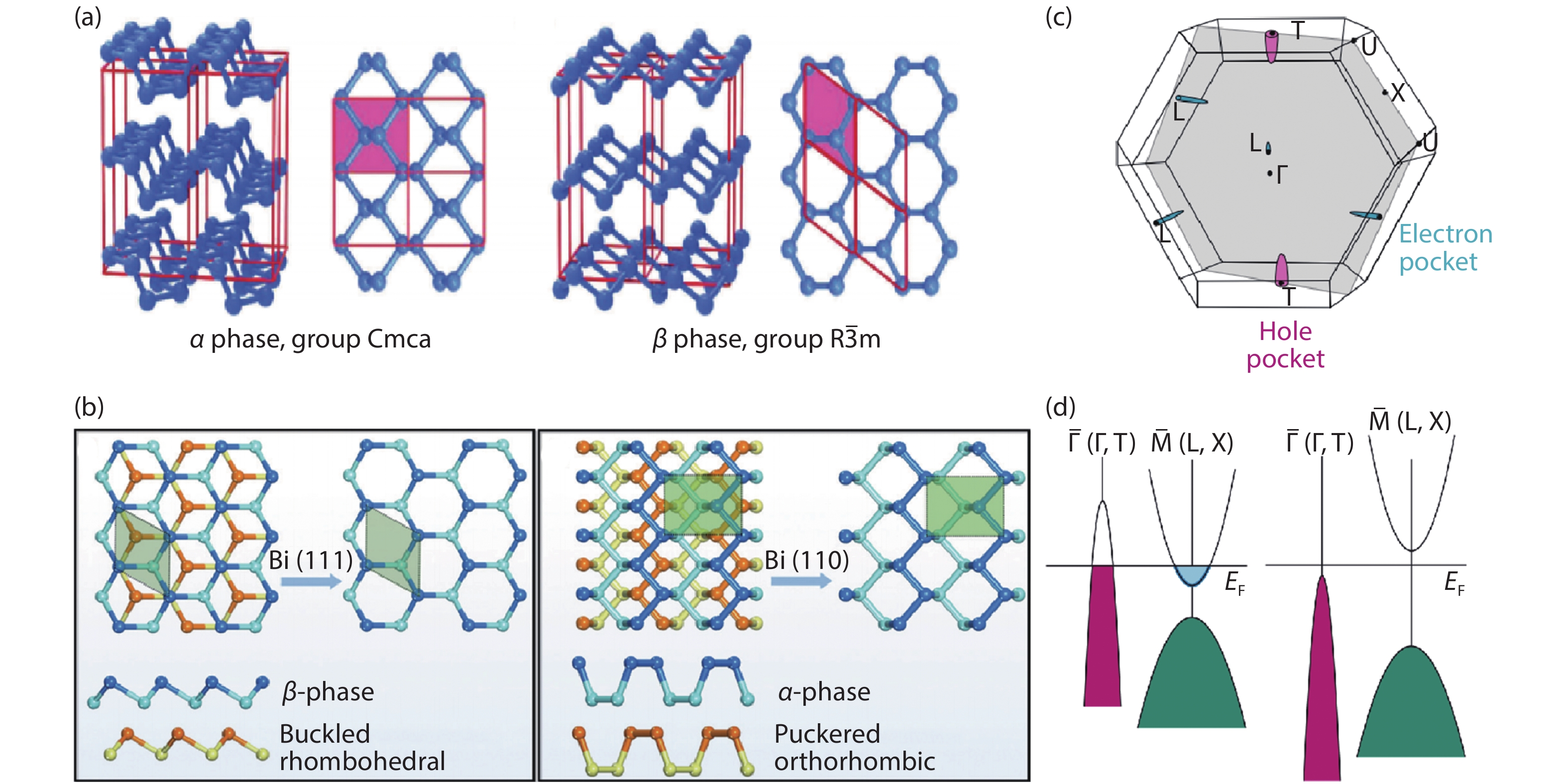
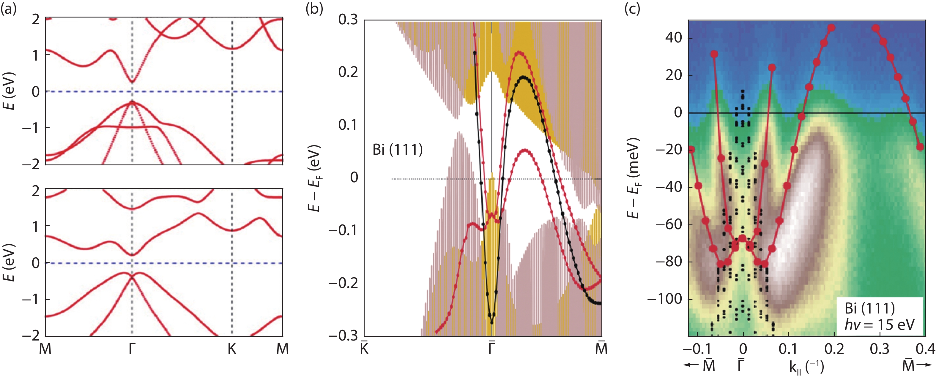
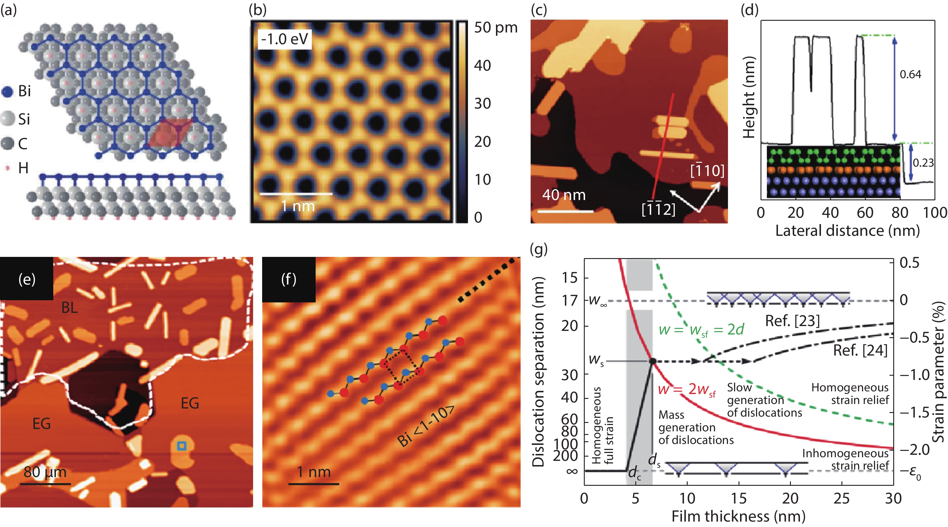
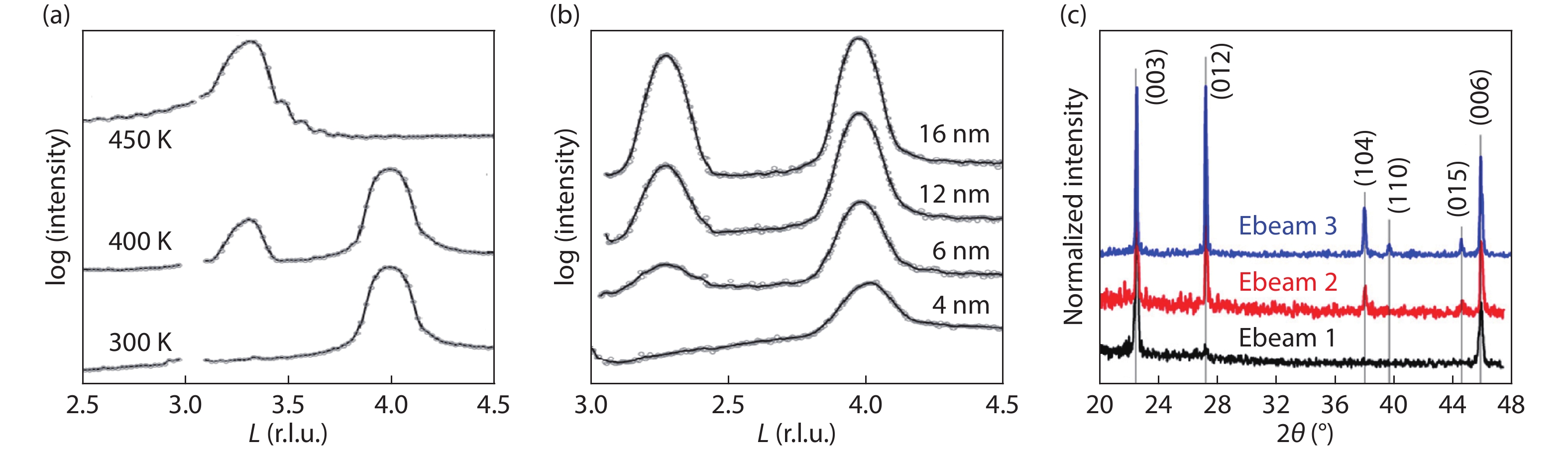
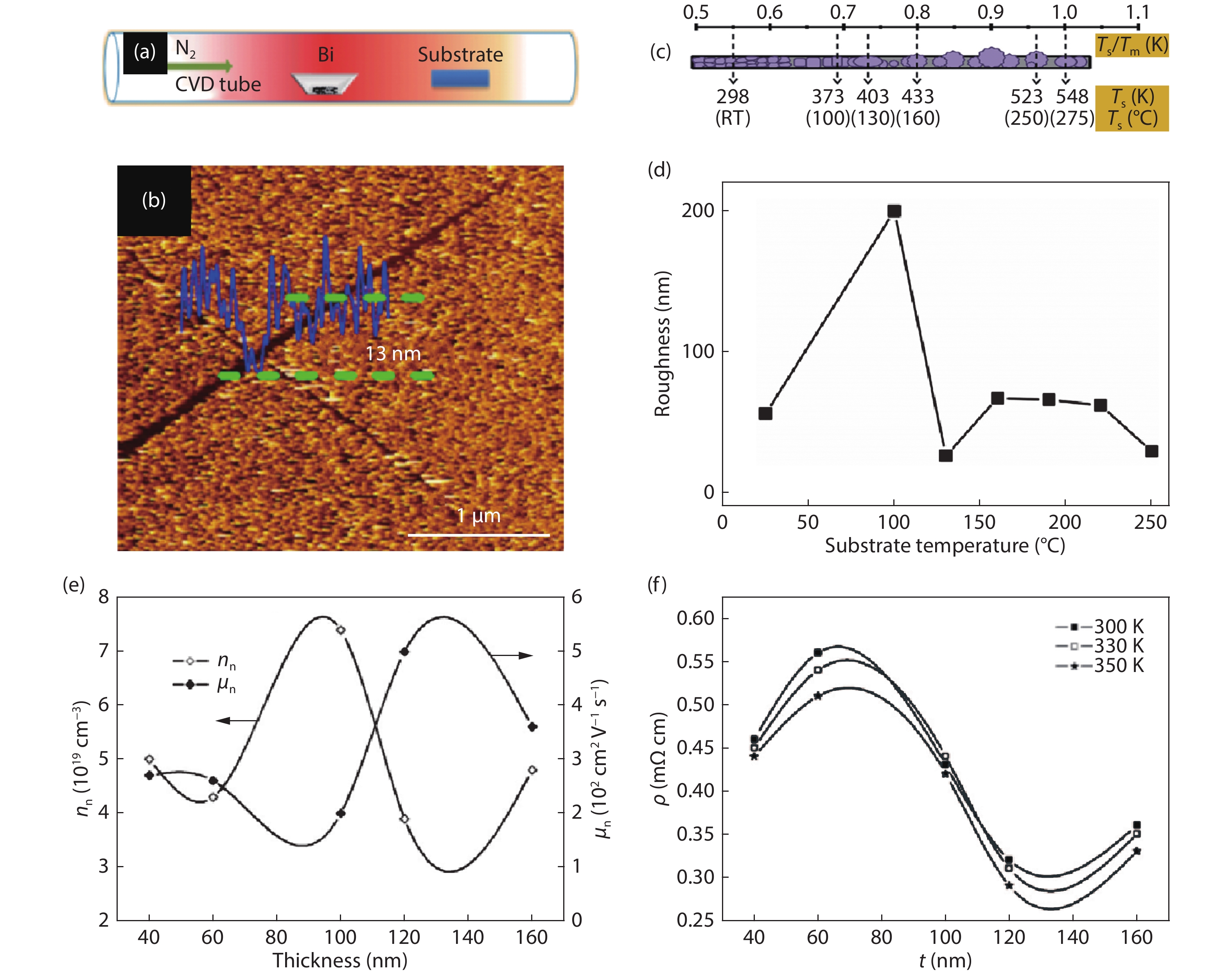
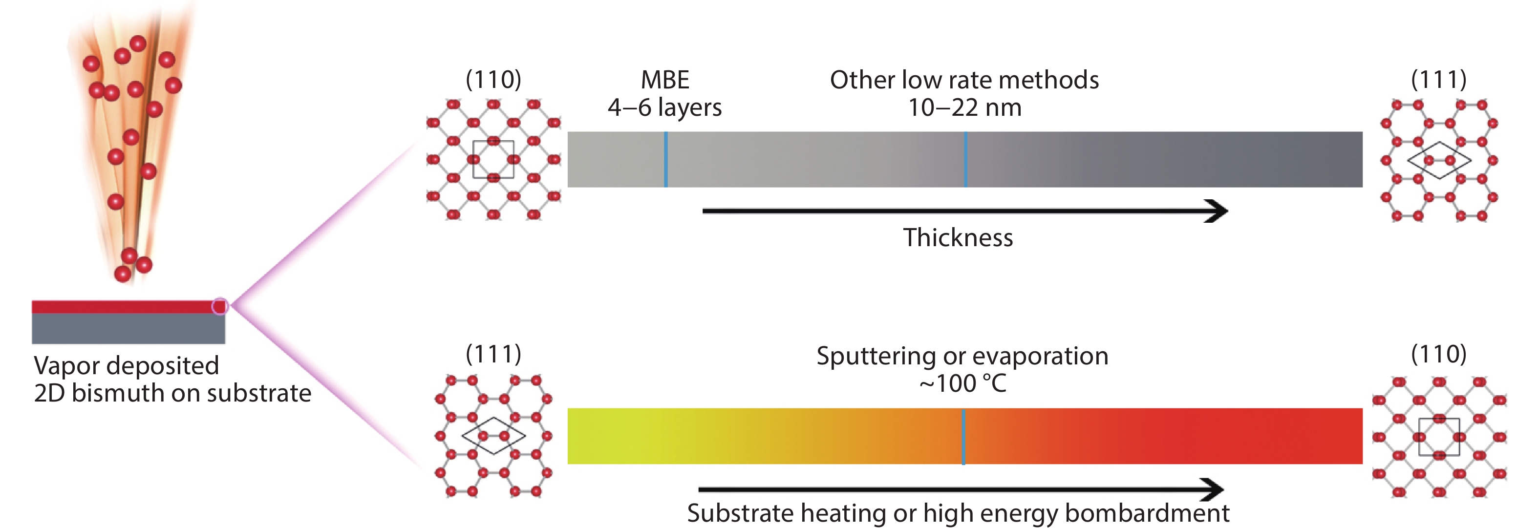
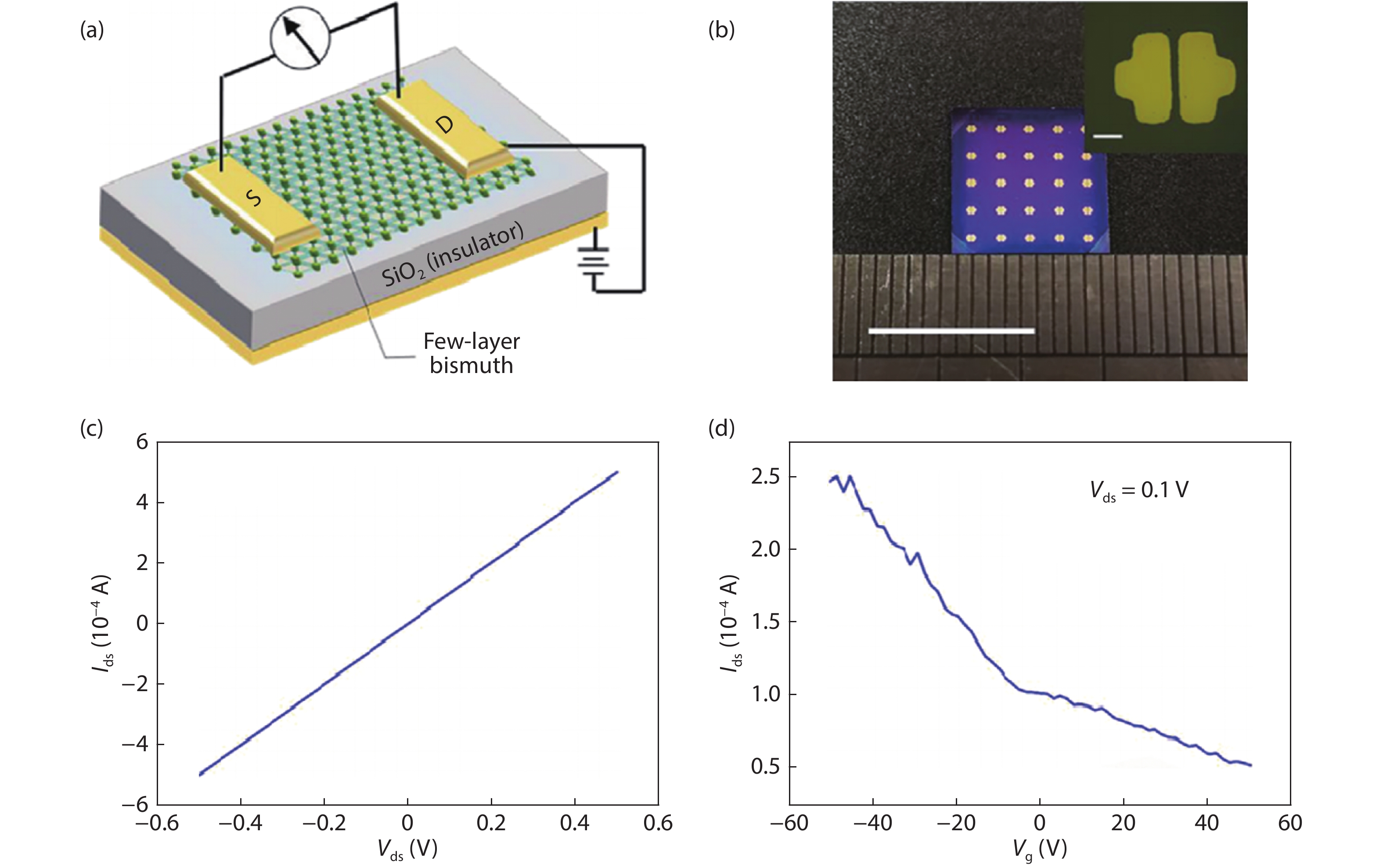
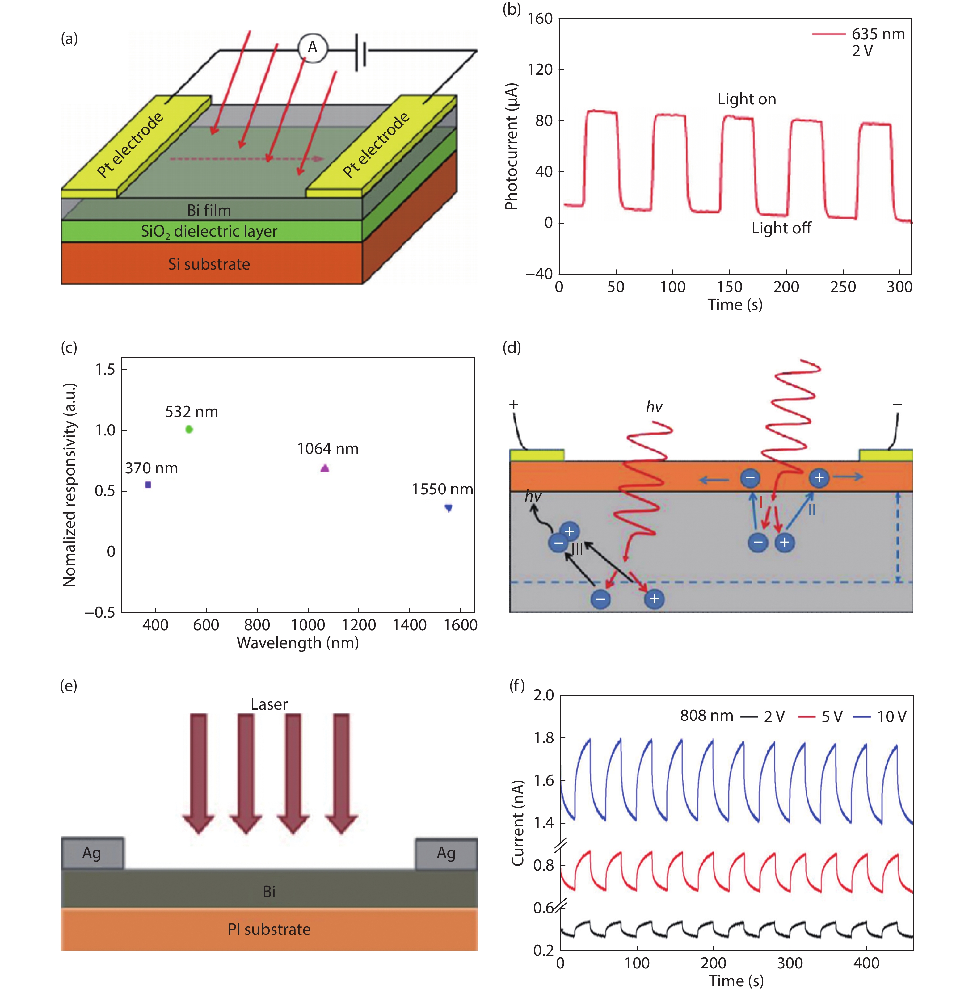
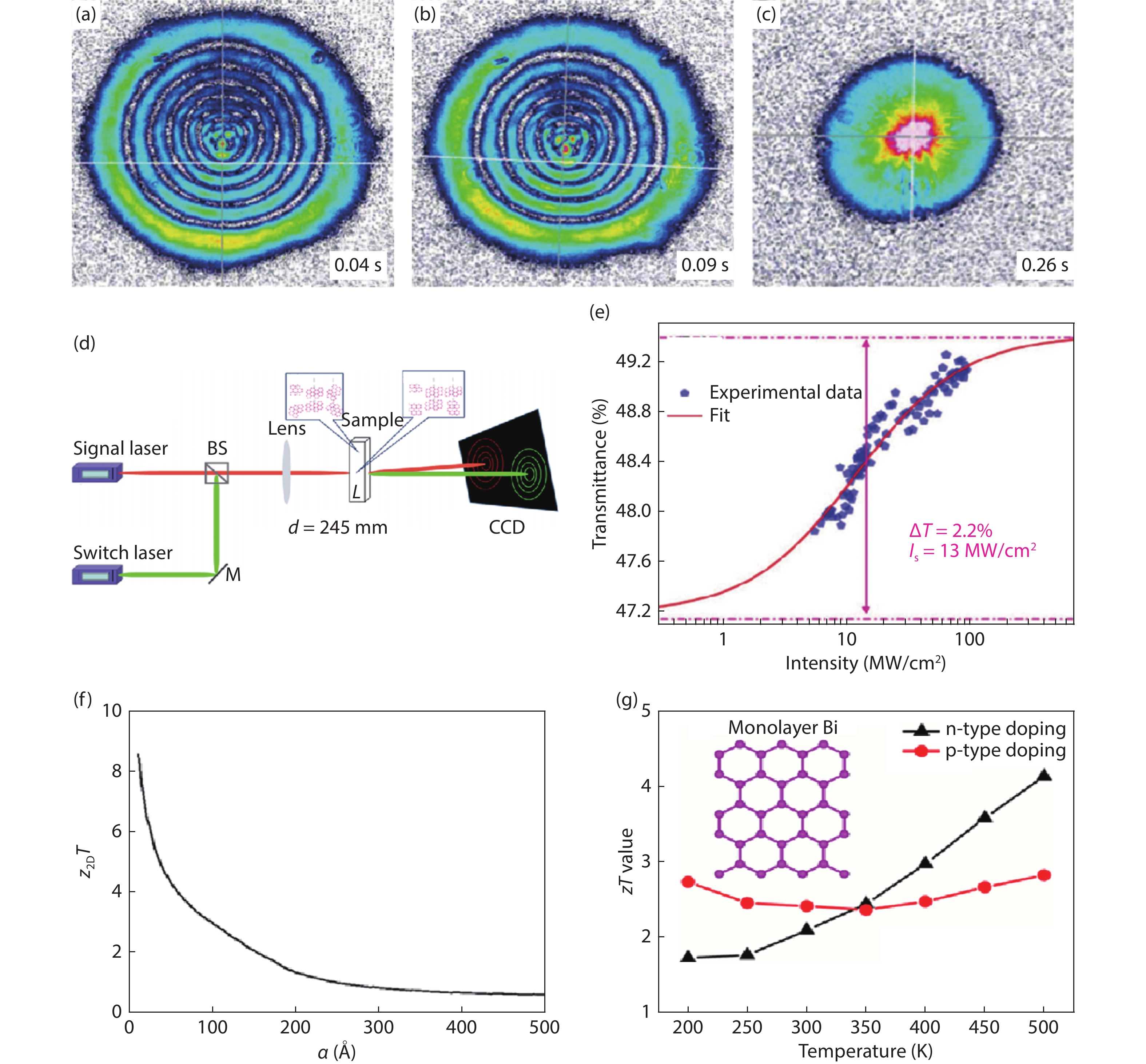
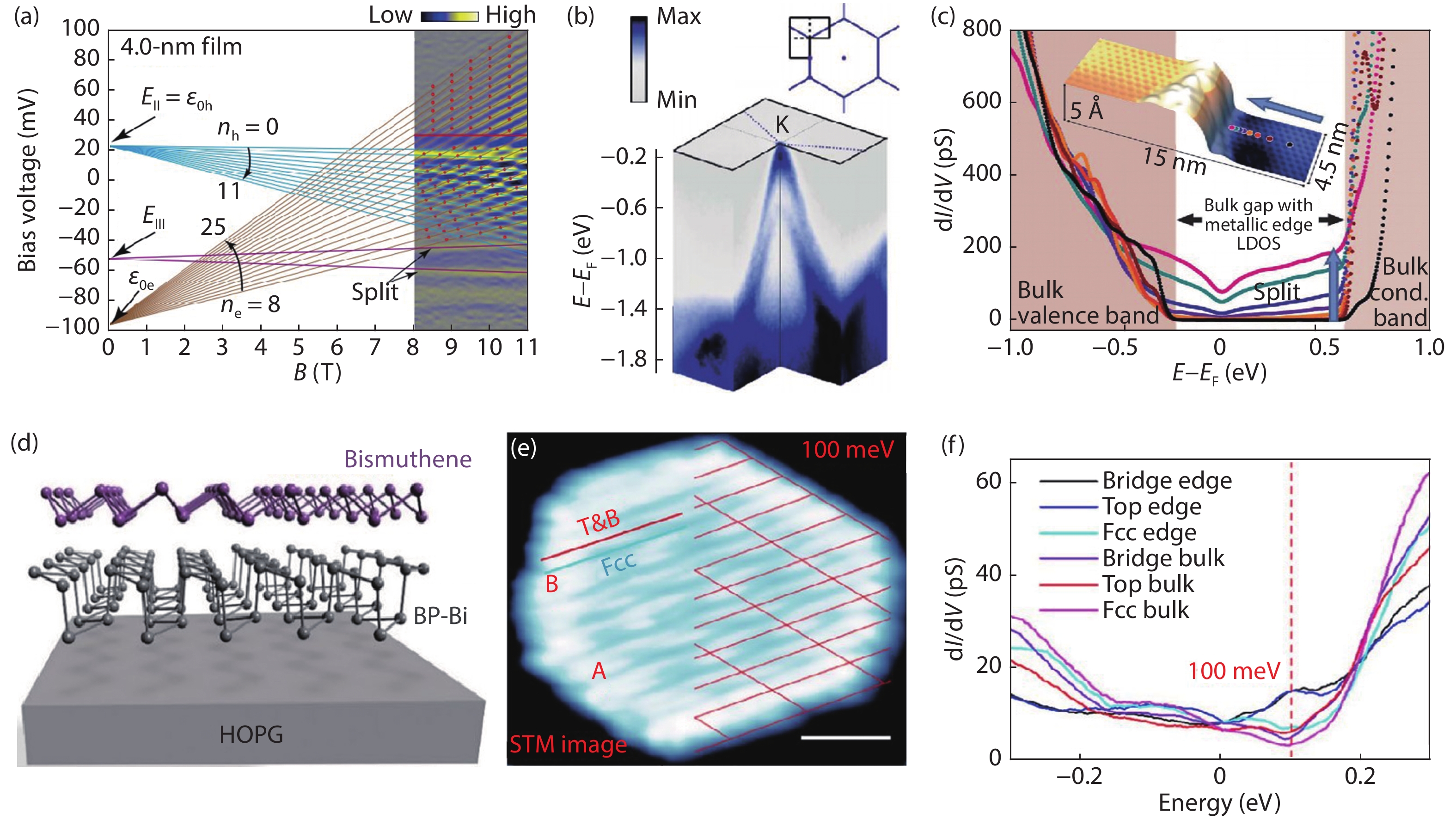
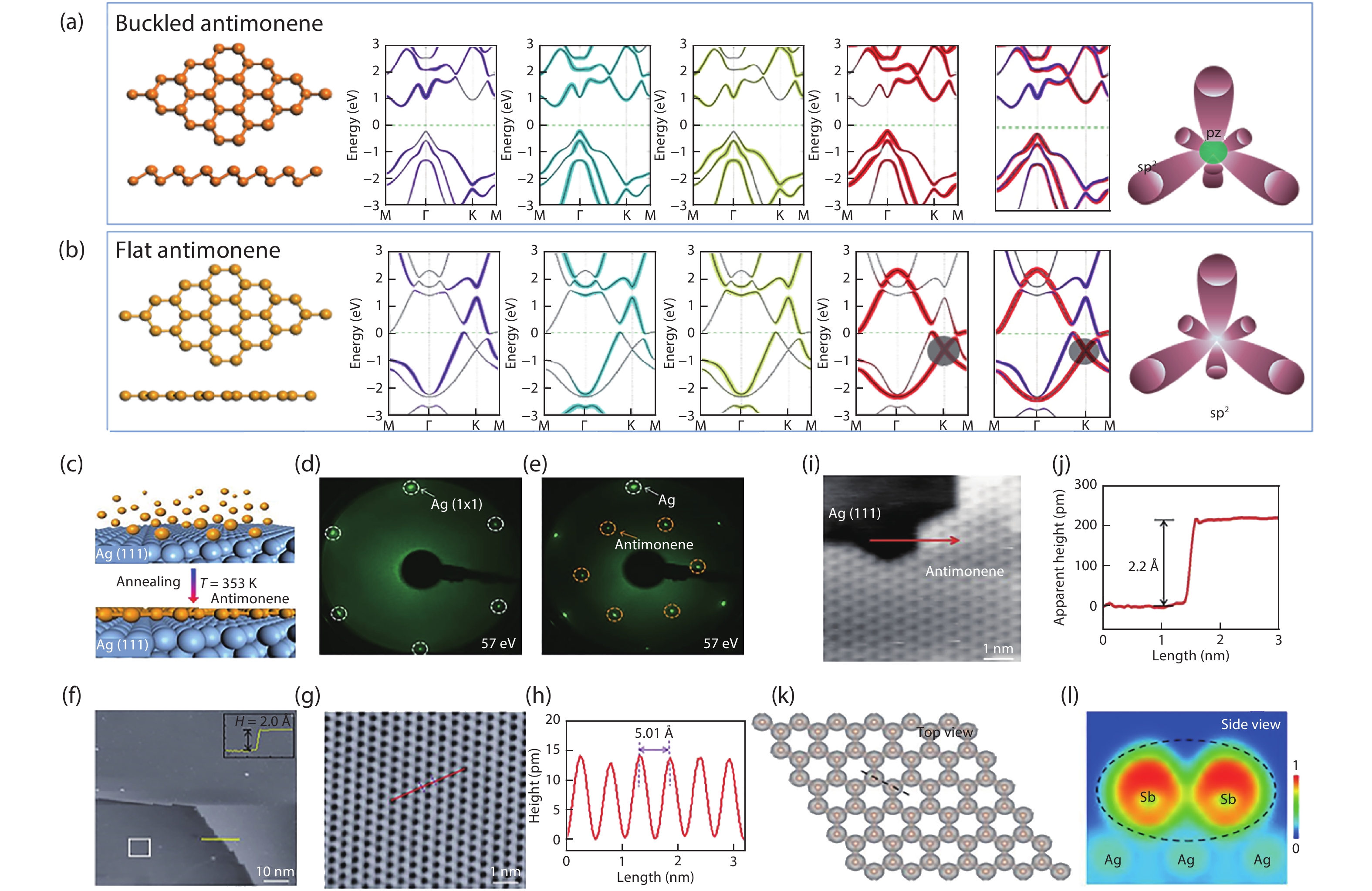
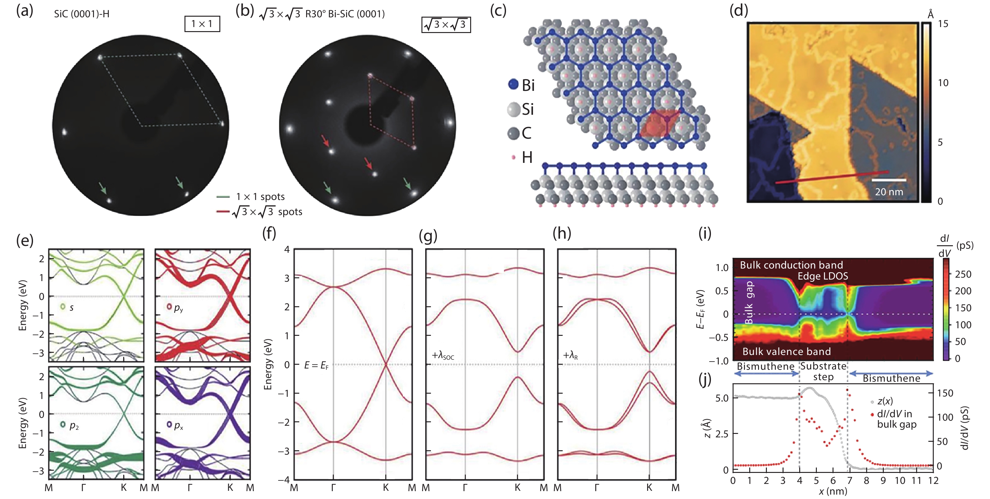
Two-dimensional (2D) bismuth, bismuthene, is an emerging pnictogen family member that has received increasing research attention in the past few years, which could yield exotic electrical, thermal, and optical properties due to unique band structure. This review provides a holistic view of recent research advances on 2D bismuth material synthesis and device applications in complementary metal oxide semiconductor (CMOS) technology. Firstly, the atomic and band structure of bismuthene is reviewed as the fundamental understanding of its physical properties. Then, it highlights material synthesis of 2D bismuth atomic sheets with emphasis on physical vapor deposition method with accurate layer controllability and process compatibility with CMOS technology. Moreover, it will survey latest applications of 2D bismuth in terms of electronic, optic, thermoelectric, spintronic and magnetic nanodevices. 2D bismuth derivatives (Bi–X, X = Sb, Te, Se) will also be mentioned as a promising strategy to further improve device performance. At last, it concludes with a brief summary on the current challenges and future prospects in 2D bismuth and its derivatives for innovative electronics, sensors and other devices compatible with CMOS techniques.

J. Semicond.
2020, 41(8): 081002 doi: 10.1088/1674-4926/41/8/081002
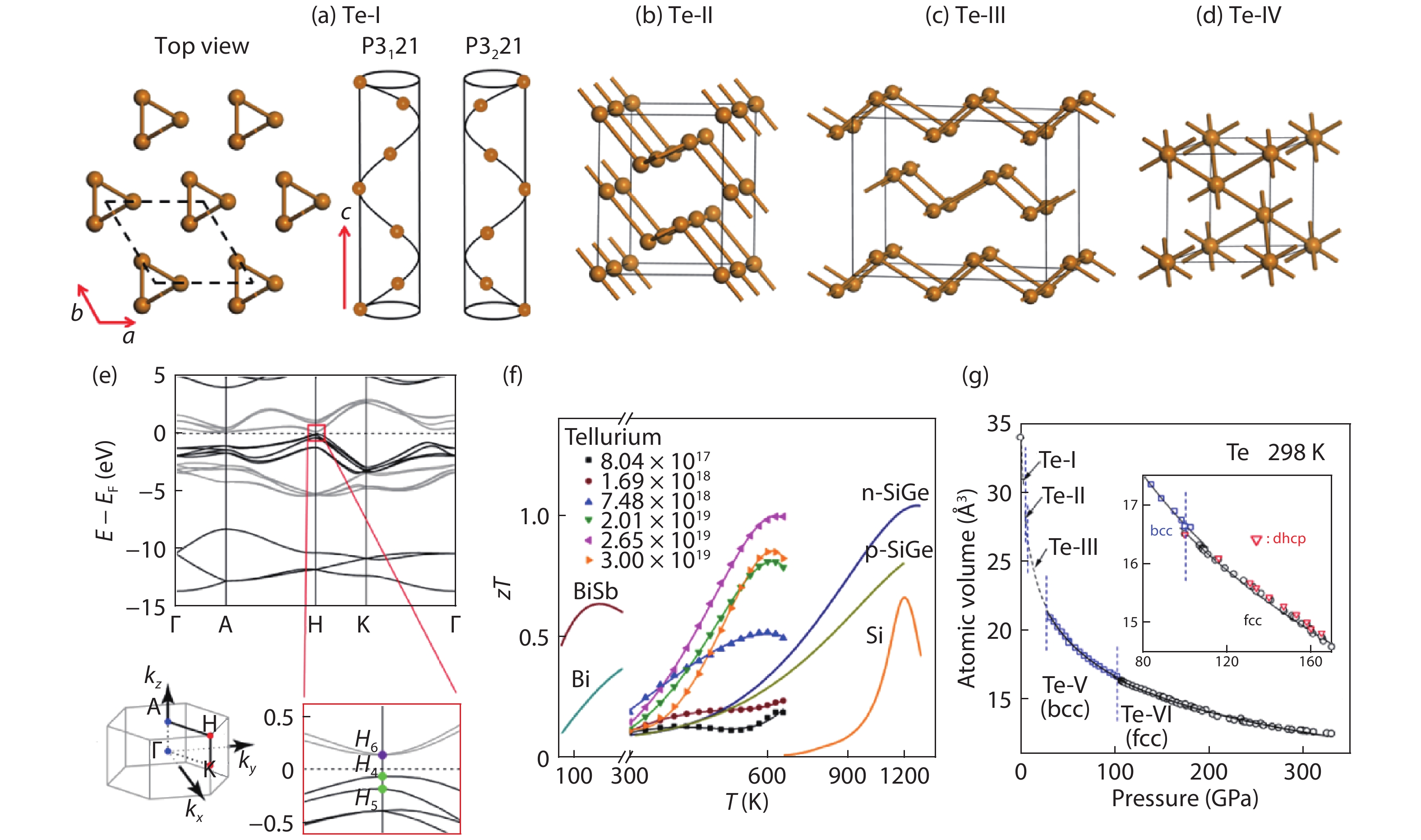
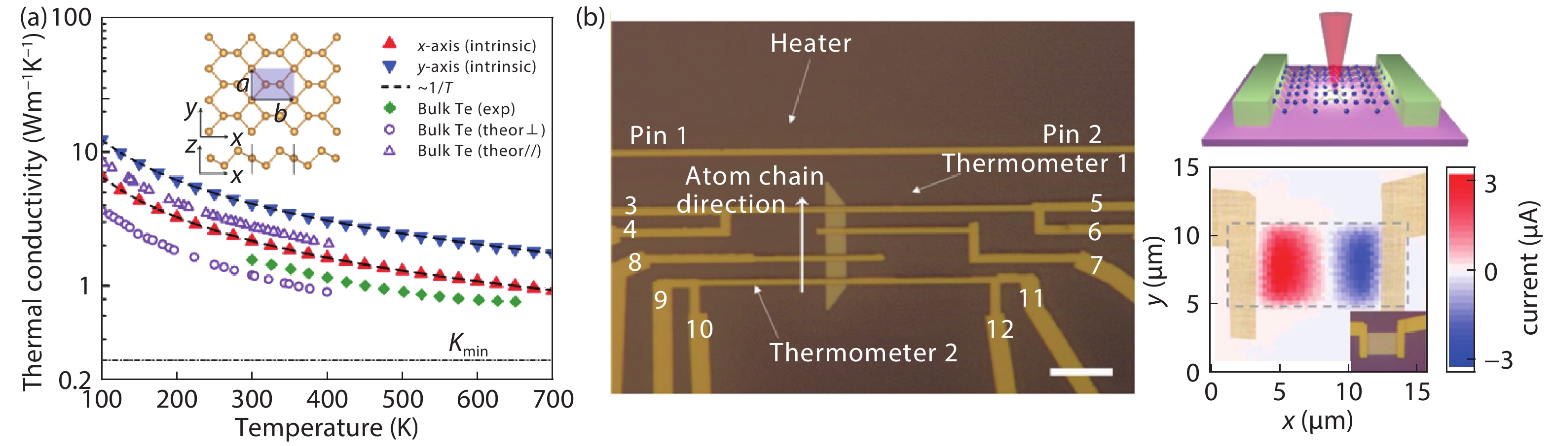
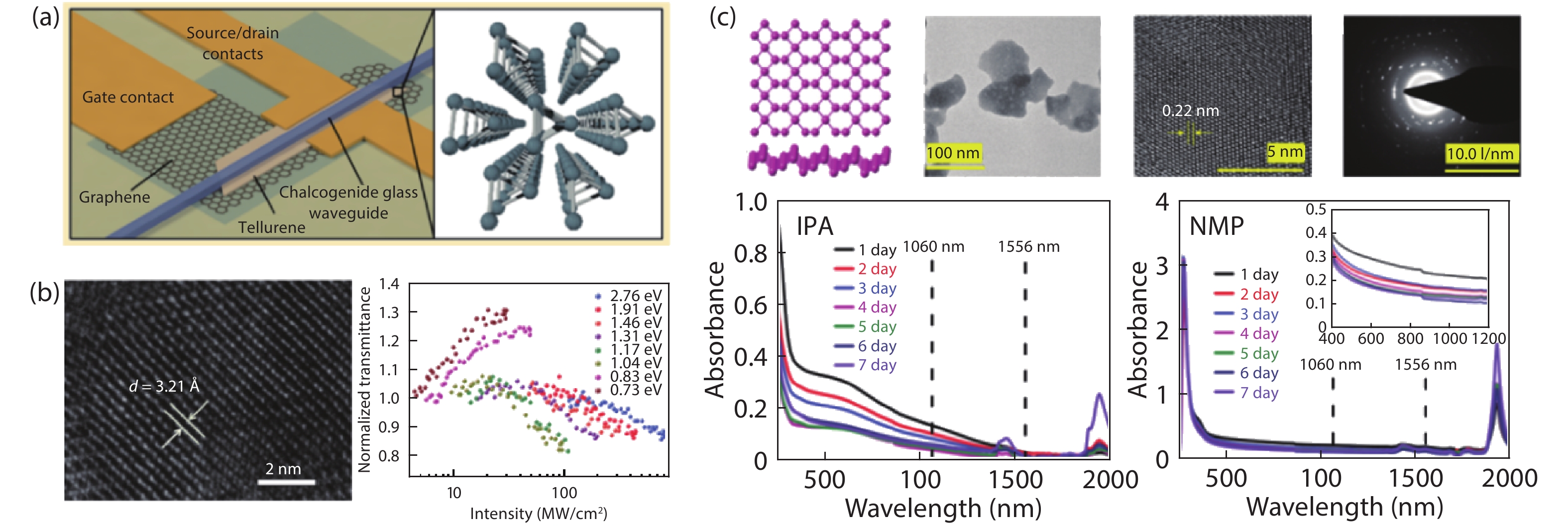
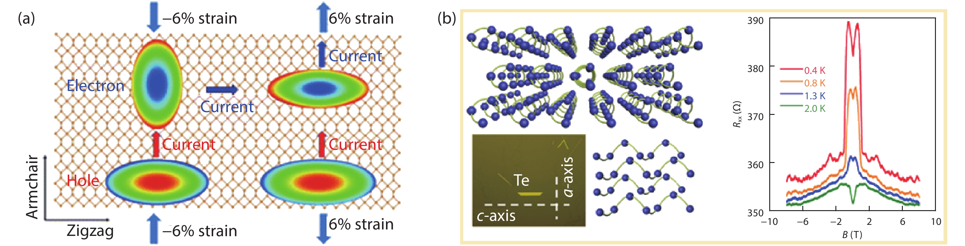
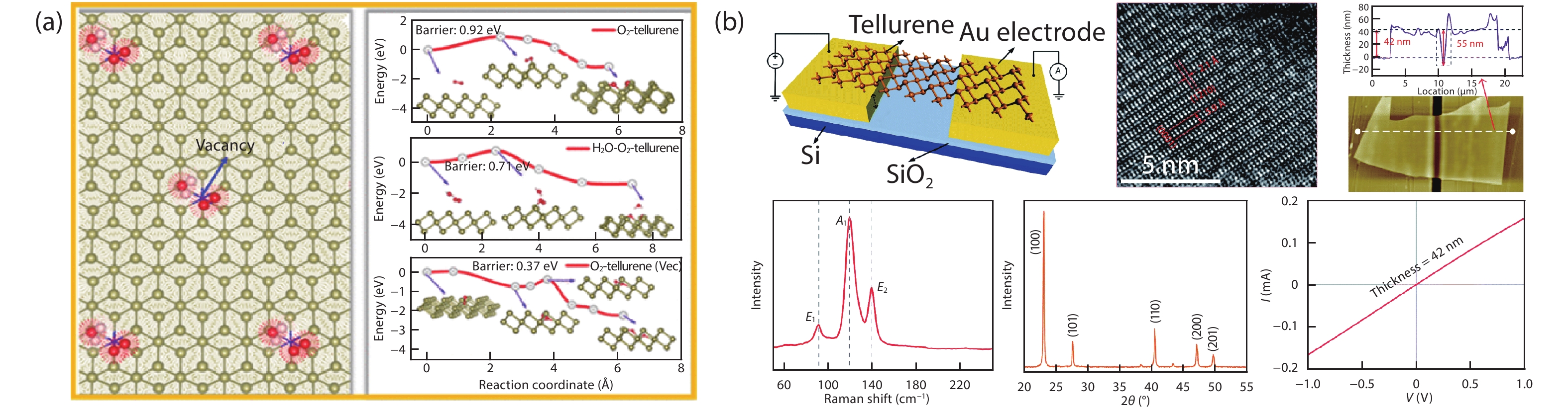
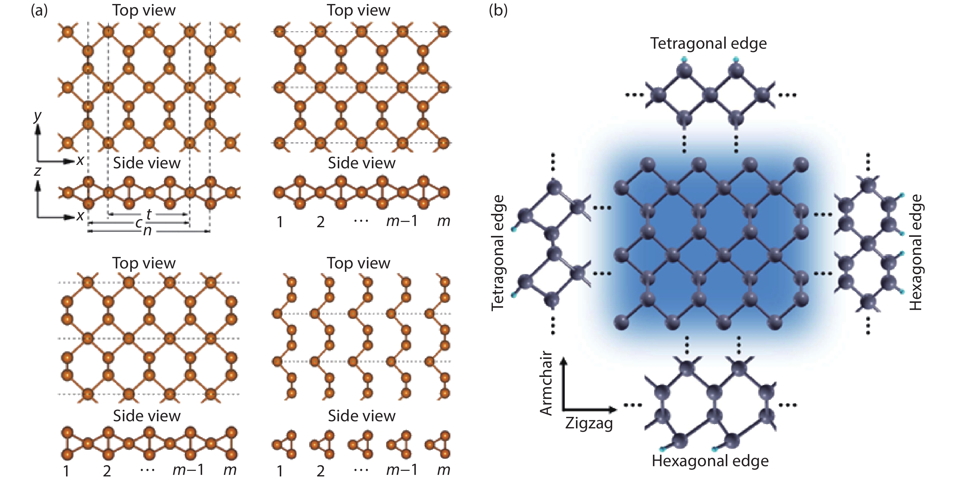
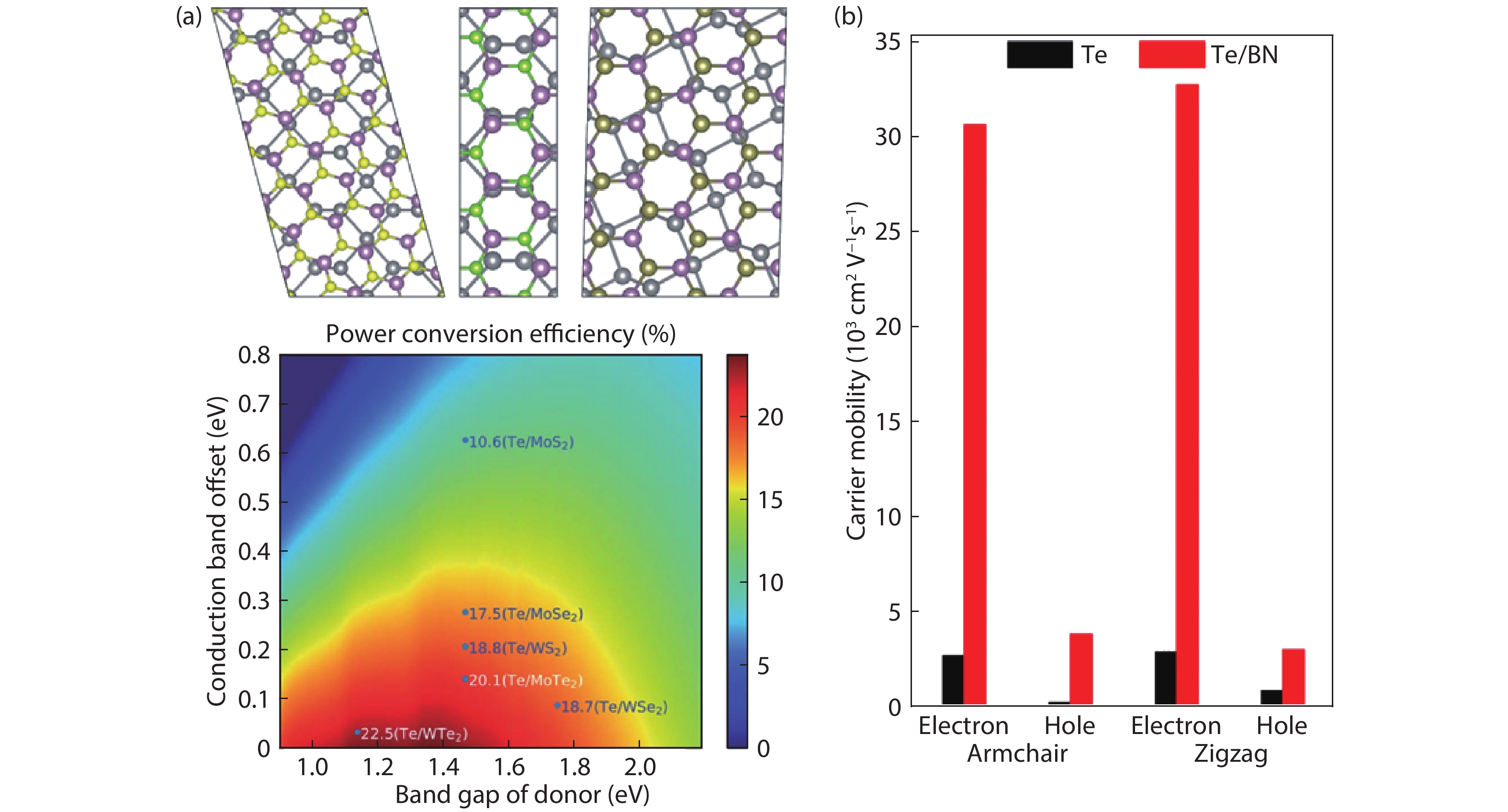
Due to the quantum confinement effect, atomically thin two-dimensional (2D) monolayer materials possess distinct characteristics from their corresponding bulk materials, which have received wide attention from science and industry. Among all the 2D materials, elemental 2D materials with the simplest components are most striking. As an emerging group-VIA elemental 2D monolayer material, tellurene exhibits many exciting fundamental properties, such as chemical and mechanical stabilities, bandgap and high carrier mobilities compared to phosphorene, graphene and MoS2, respectively. Besides, in further exploration, it was found that tellurene or tellurene-based device presents excellent thermoelectric properties, piezoelectric properties, quantum Hall effects, and superb optical properties especially nonlinear optics characteristics, etc. The properties of tellurene can be modulated by virtue of strain, defects, edges, and heterojunction effects. In view of so many unique properties, it has drawn significant interest since tellurene was predicted and fabricated successfully in 2017. In this paper, we review the 2D tellurene allotropes, experimental preparation, excellent properties, performance modulation and future development.


J. Semicond.
2020, 41(8): 081003 doi: 10.1088/1674-4926/41/8/081003
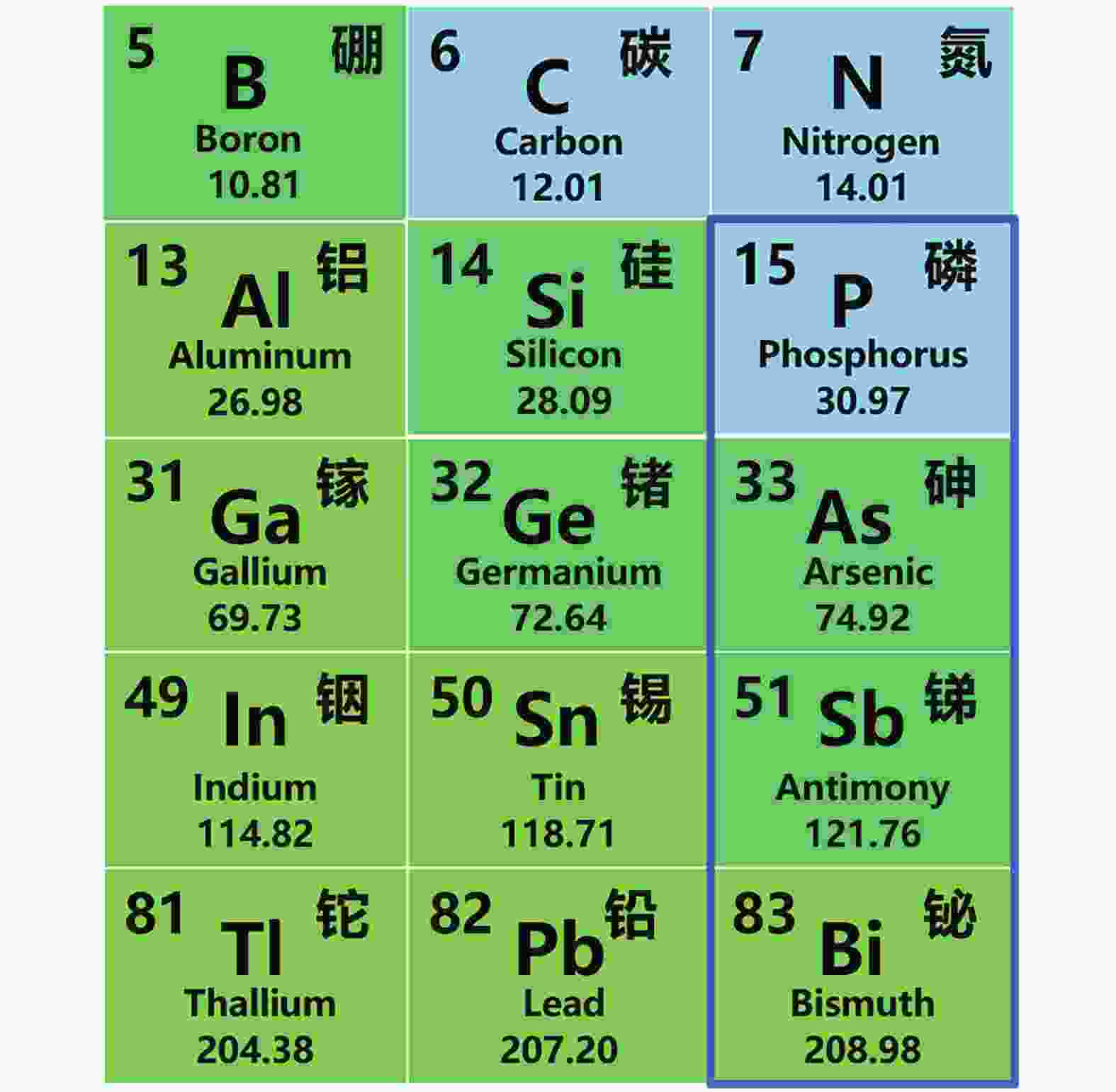
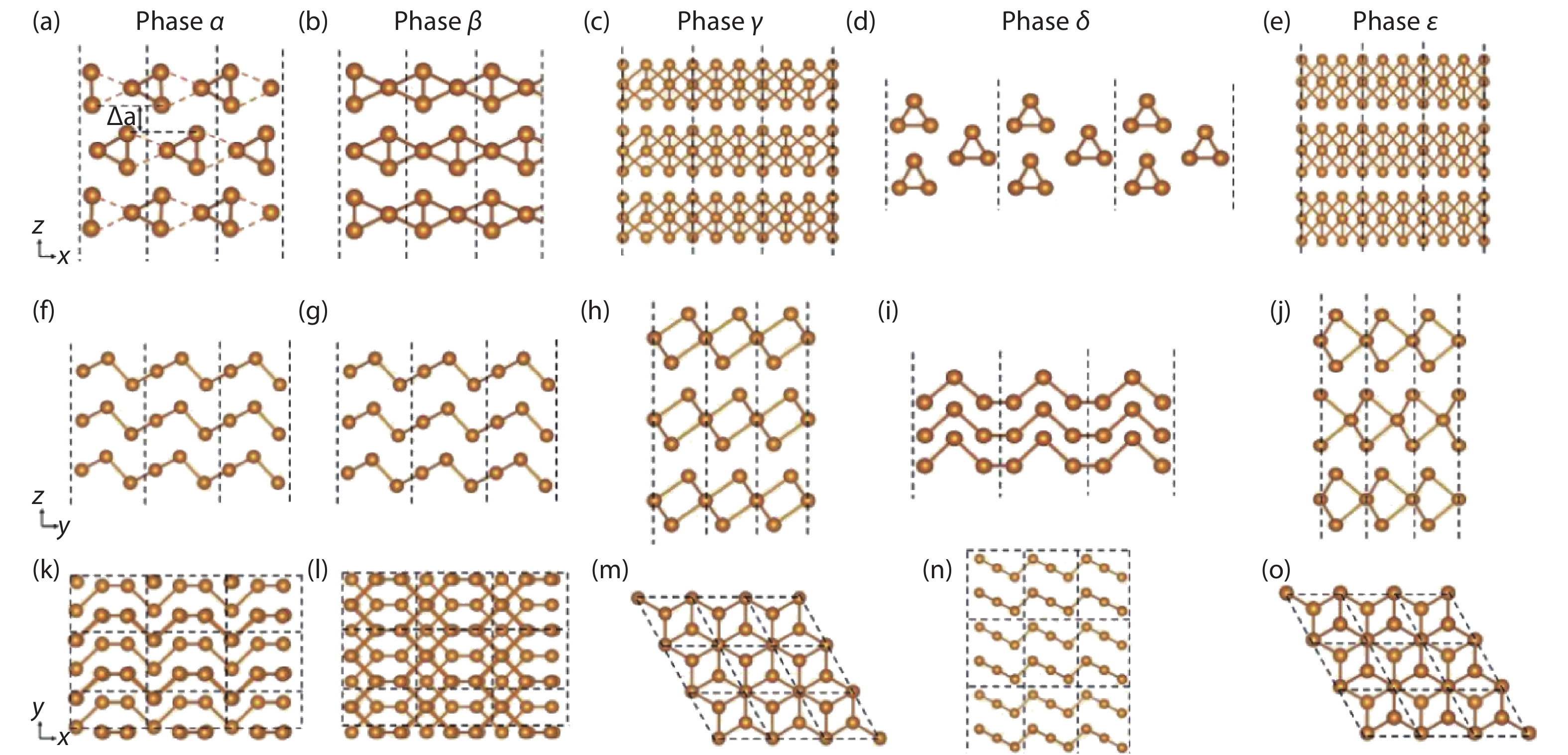
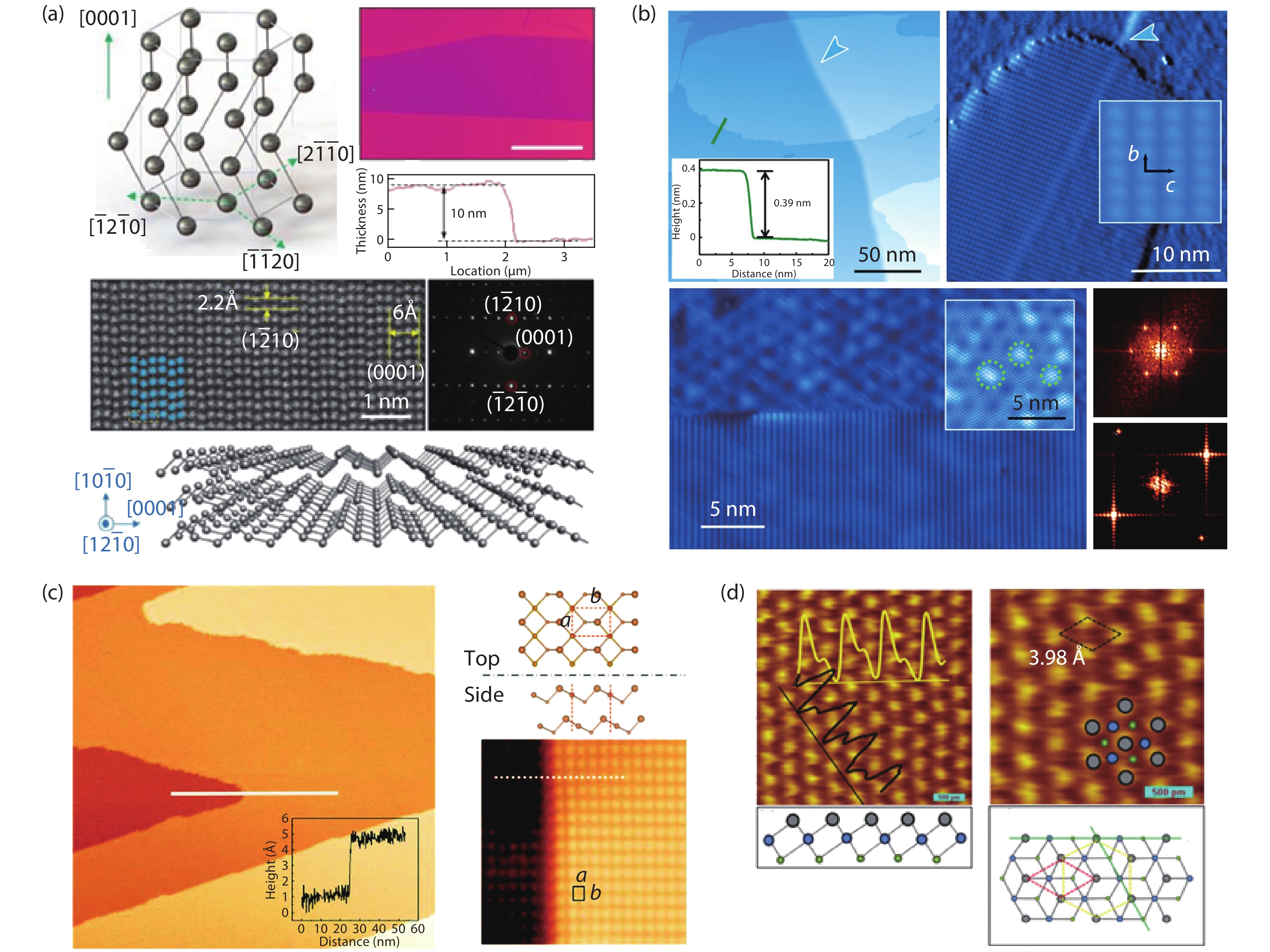
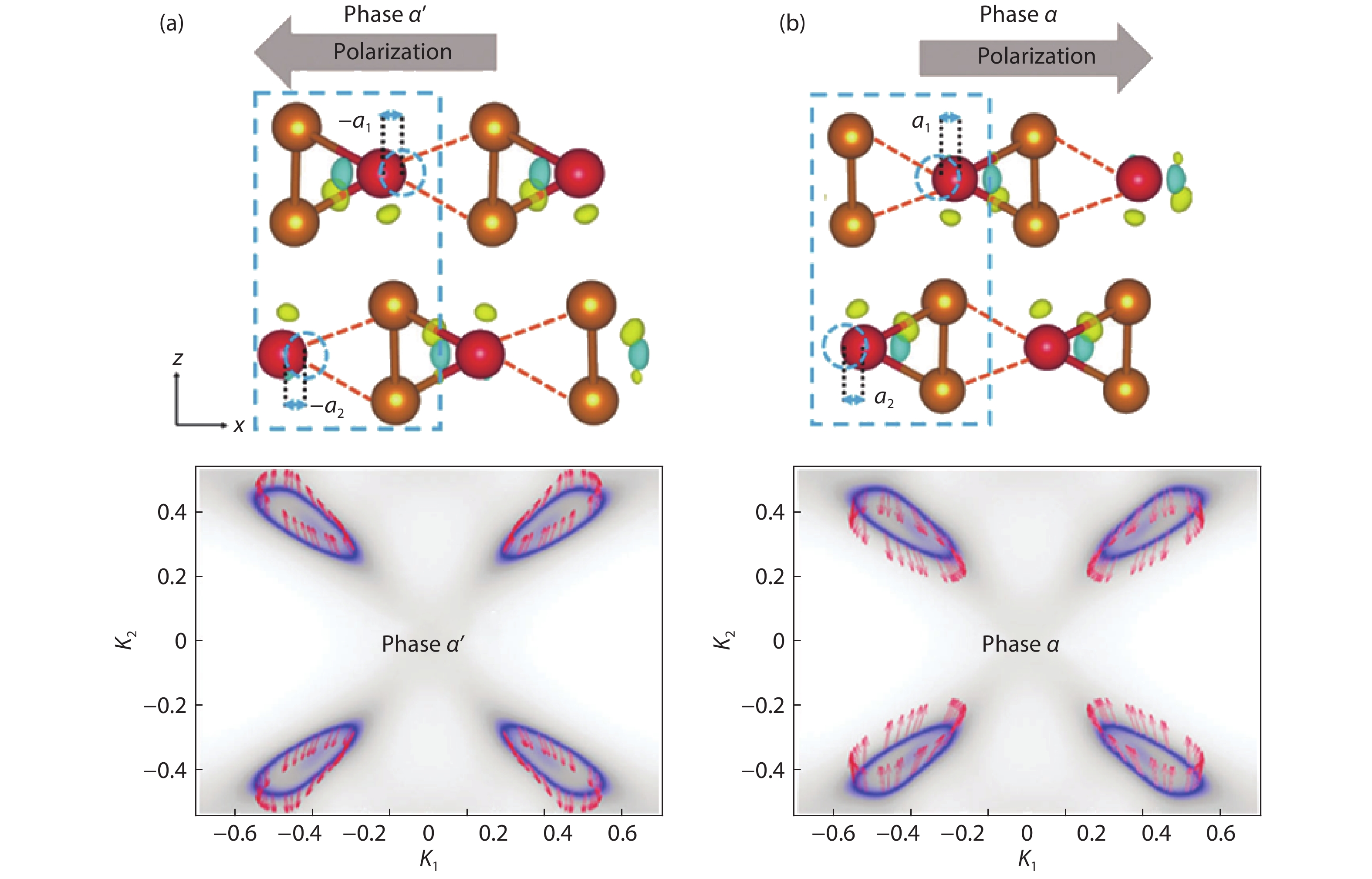
A large number of two-dimensional (2D) monoelemental materials with huge application potentials have been developed, since graphene was reported as a monoelemental material with unique properties. As cousins of graphene, 2D group-V elemental monolayers have gained tremendous interest due to their electronic properties with significant fundamental bandgap. In this review, we extensively summarize the latest theoretical and experimental progress in group-V monoelemental materials, including the latest fabrication methods, the properties and potential applications of these 2D monoelementals. We also give a perspective of the challenges and opportunities of 2D monoelemental group-V monolayer materials and related functional nanodevices.


J. Semicond.
2020, 41(8): 082001 doi: 10.1088/1674-4926/41/8/082001
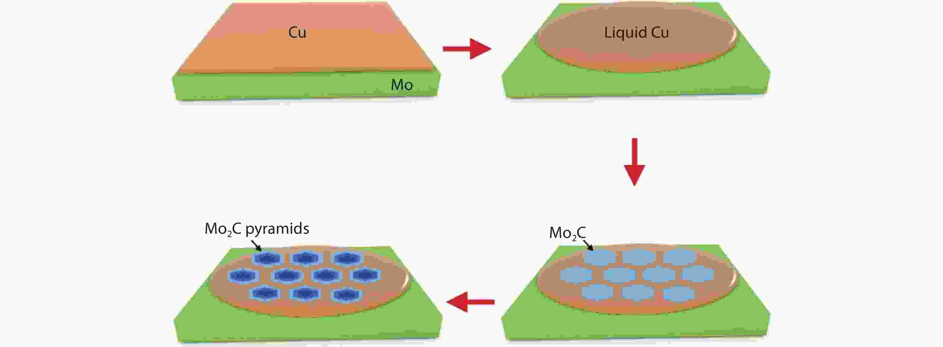
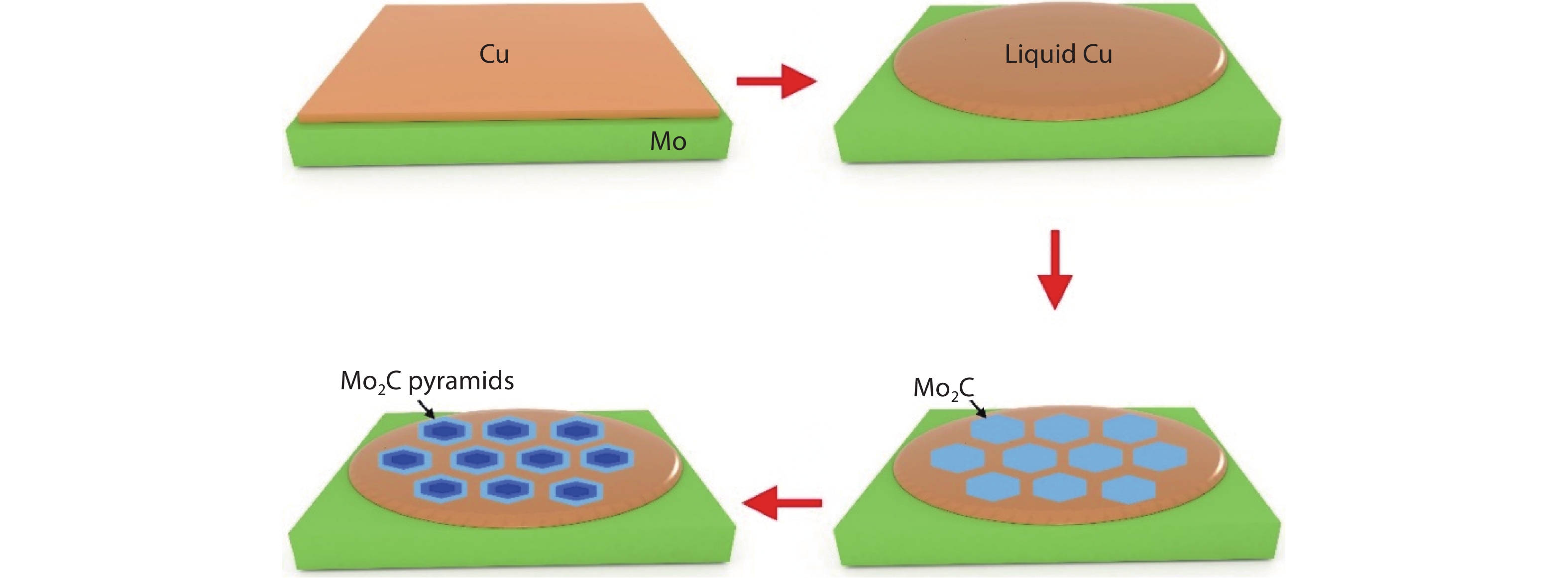
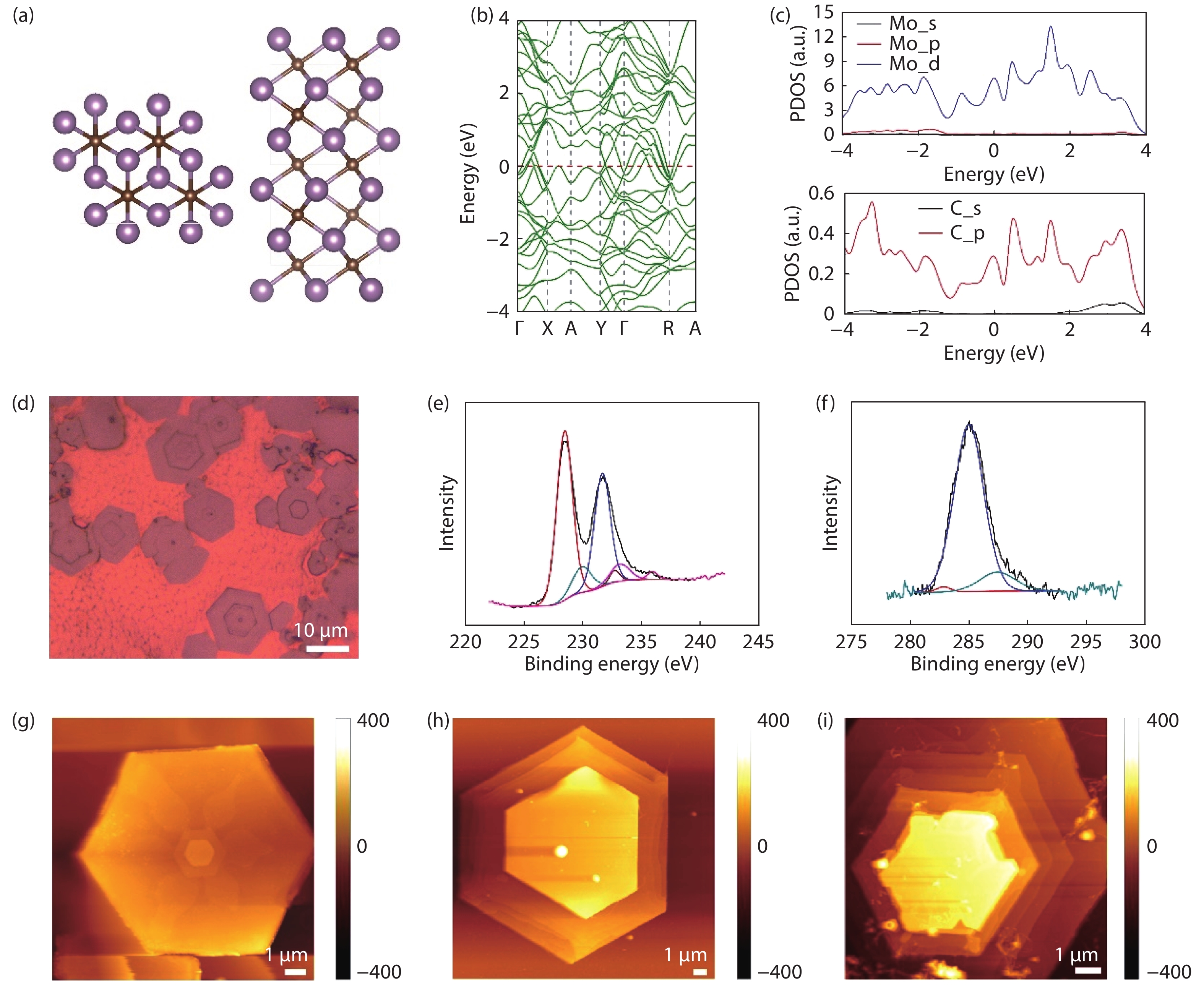
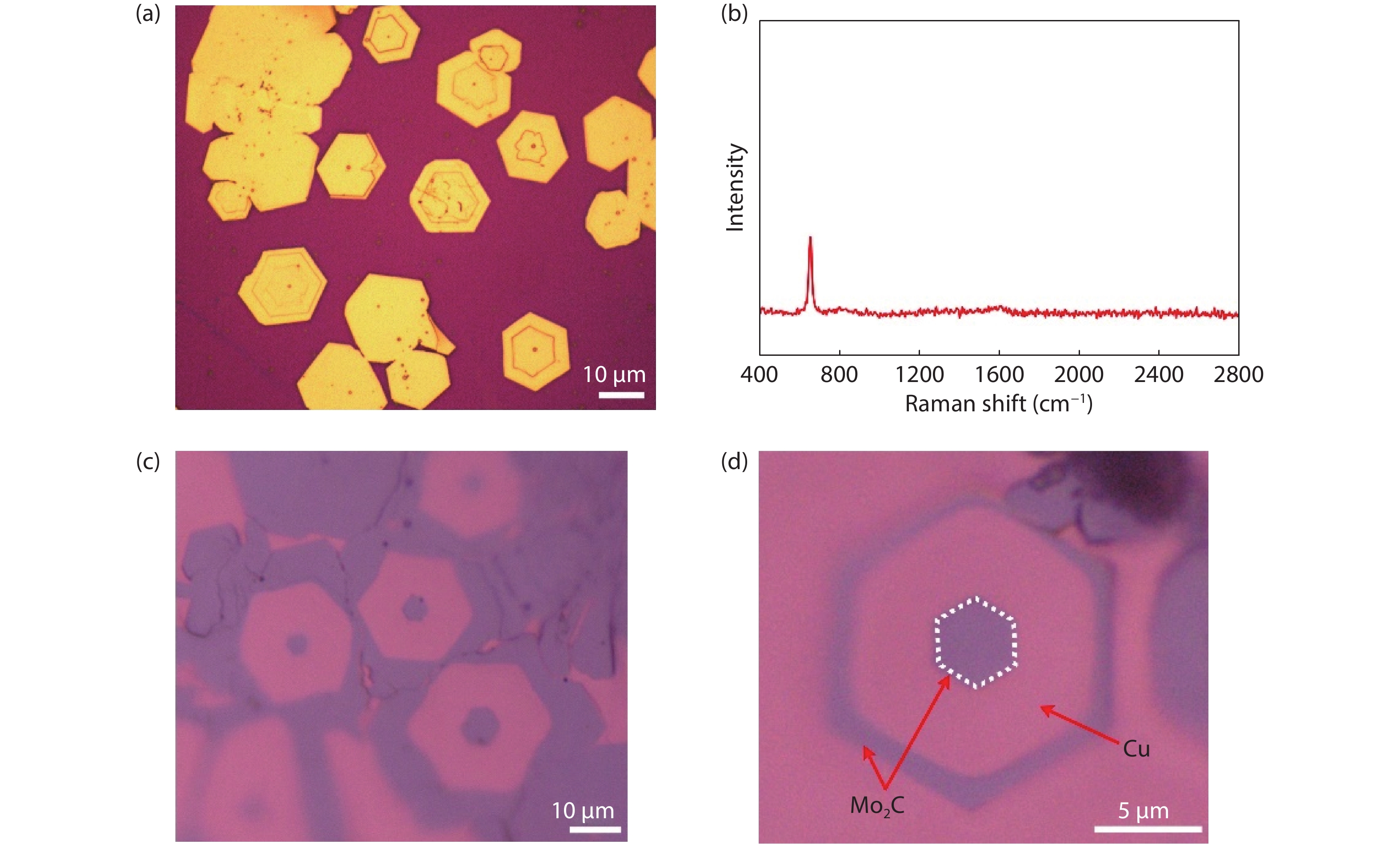
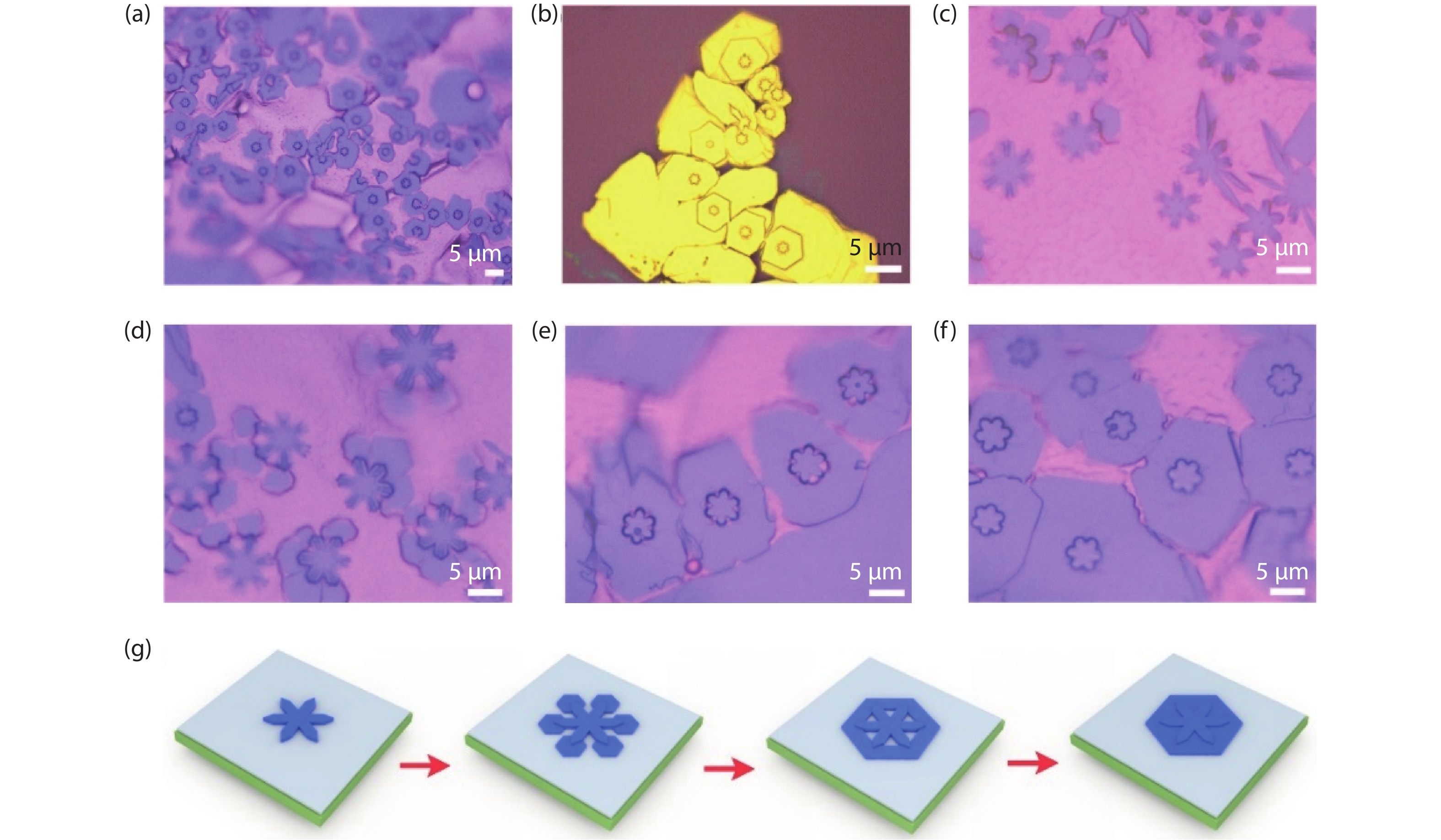
Precise spatial control of 2D materials is the key capability of engineering their optical, electronic, and mechanical properties. However, growth of novel 2D Mo2C on Cu surface by chemical vapor deposition method was revealed to be seed-induced 2D growth, limiting further synthesis of complex Mo2C spatial structures. In this research, we demonstrate the controlled growth of Mo2C pyramids with numerous morphologies, which are characterized with clear terraces within the structures. The whole evolution for Mo2C pyramids in the coursed of CVD process has been detected, posing significant potential in probing growth mechanism. The formation of the Mo2C pyramids arises from the supersaturation-induced nucleation and concentration-gradient driven diffused growth of a new Mo2C layer on the edged areas of intrinsic ones, as supported by STEM imaging. This work provides a novel Mo2C-based pyramid structure and further reveals a sliding growth mechanism, which could offer impetus for the design of new 3D spatial structures of Mo2C and other 2D materials.
J. Semicond.
2020, 41(8): 082002 doi: 10.1088/1674-4926/41/8/082002

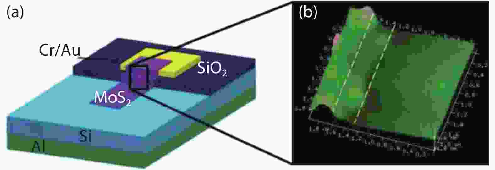
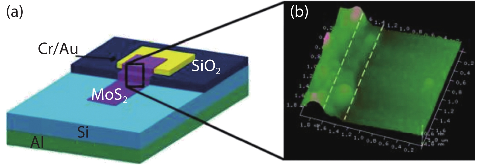
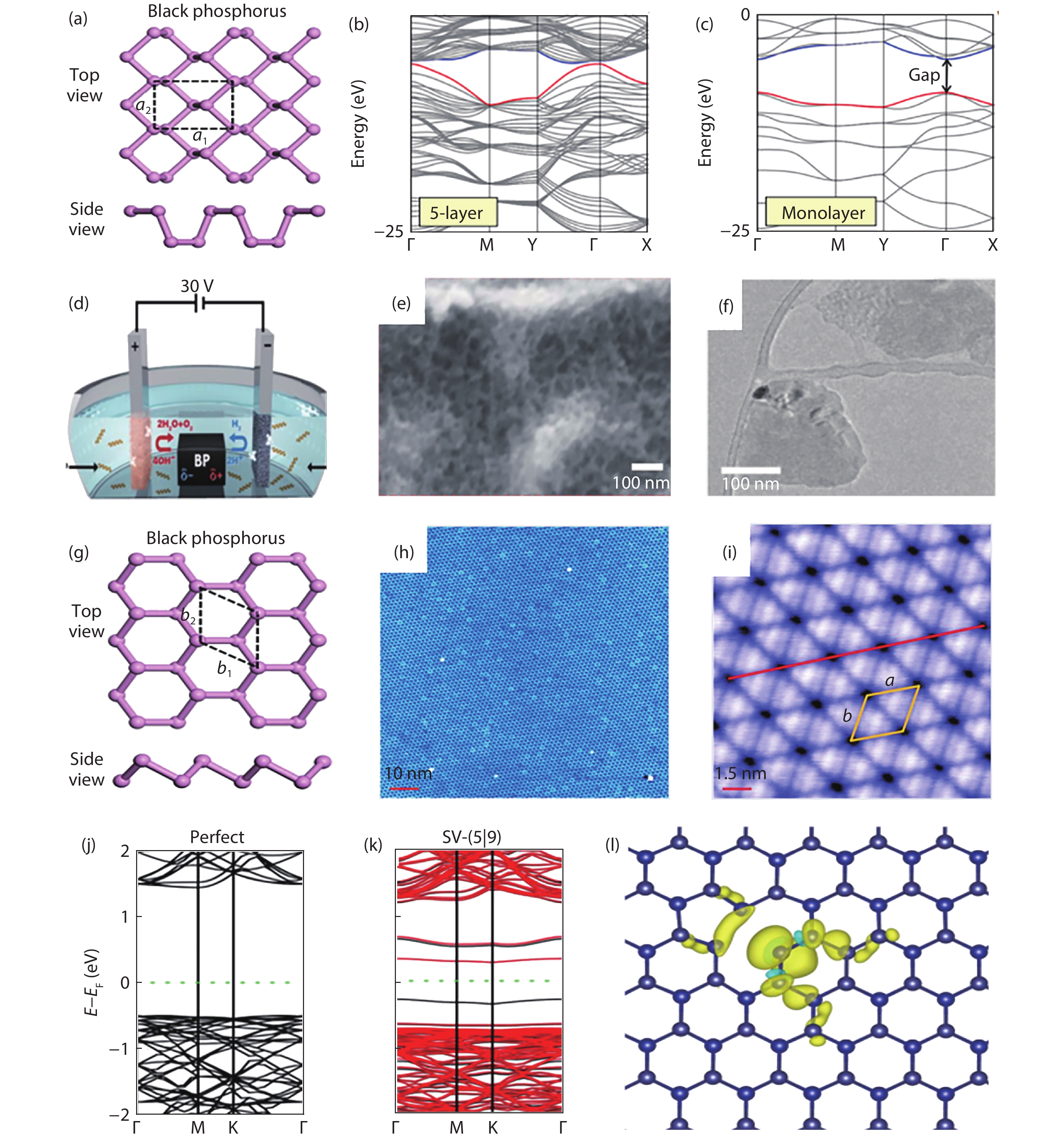
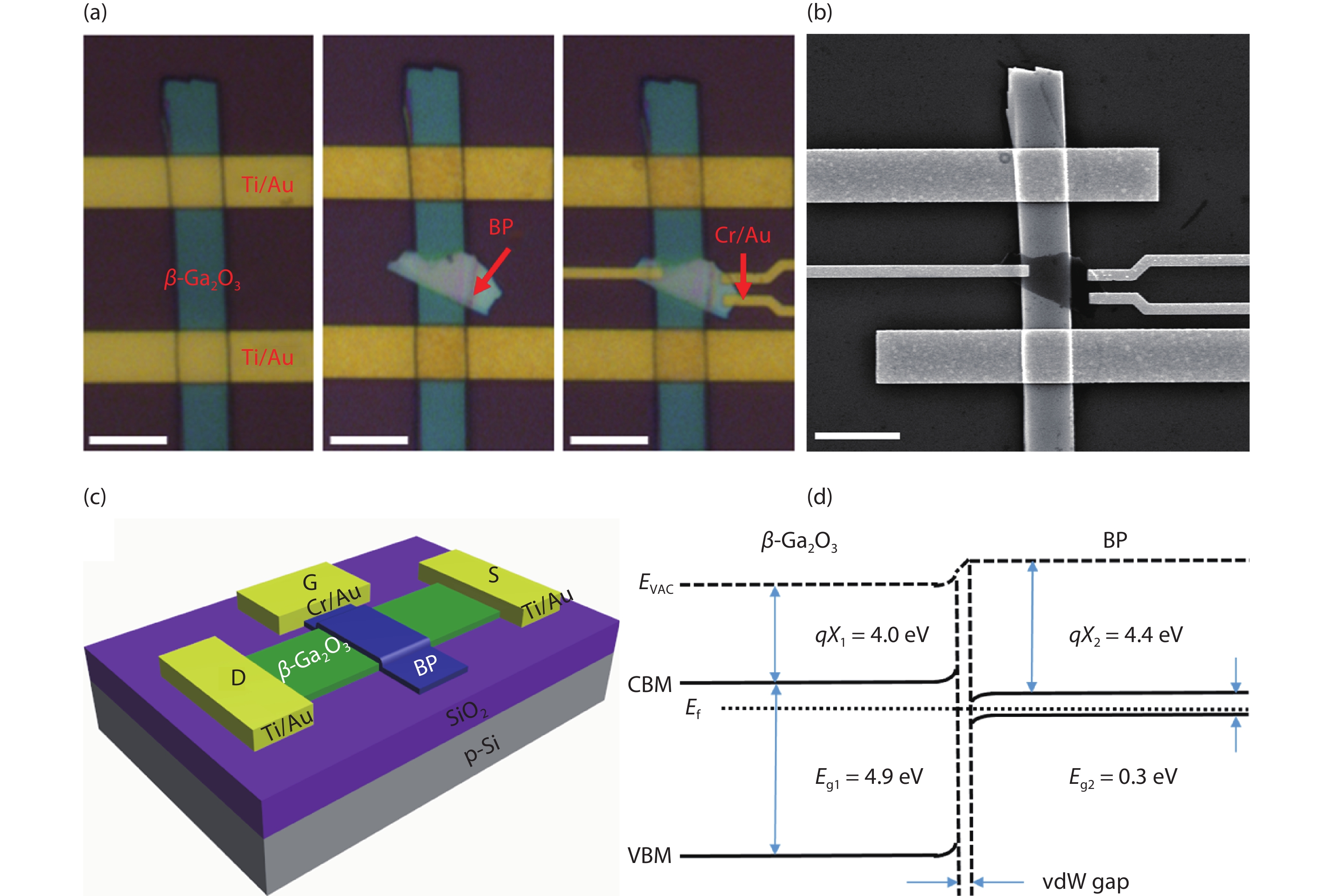
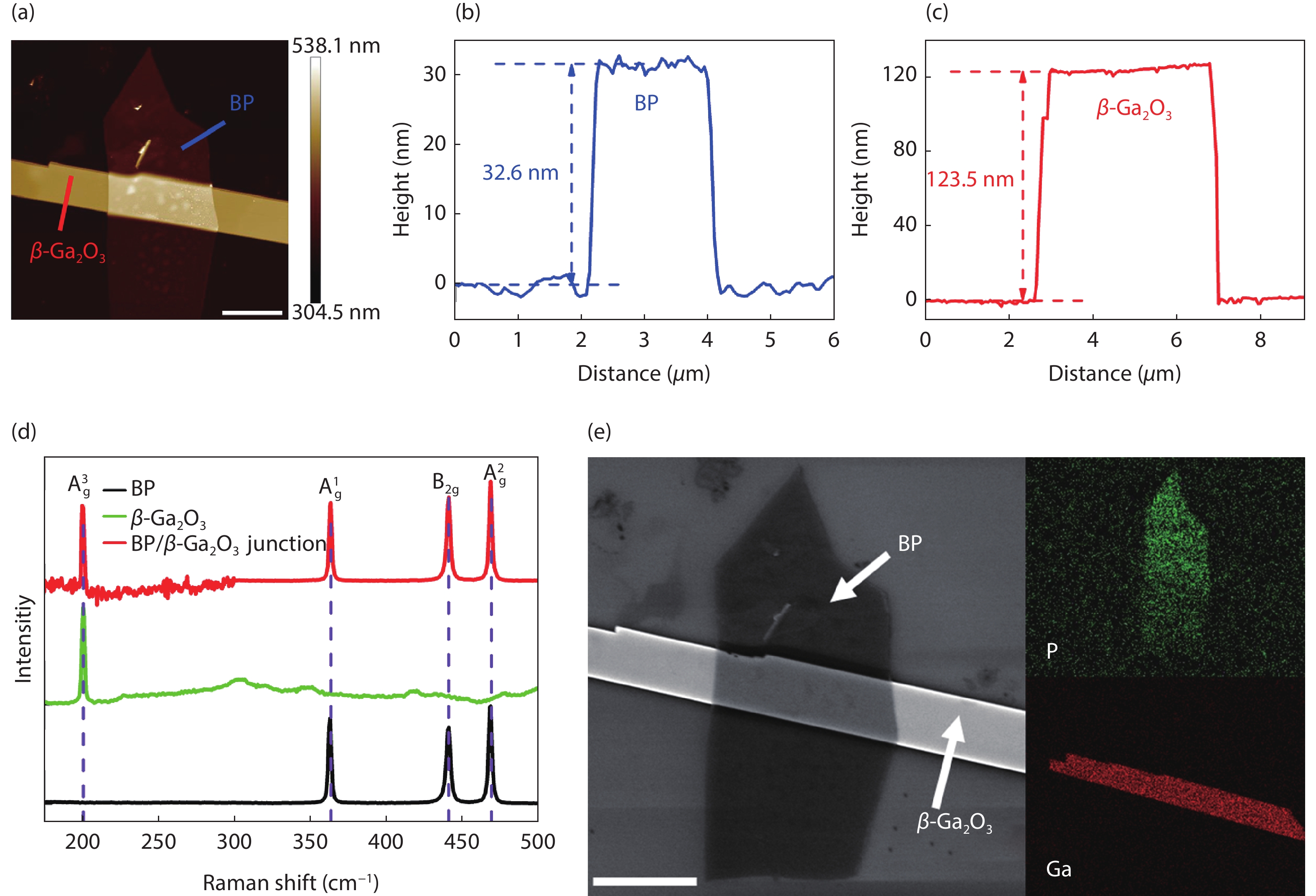
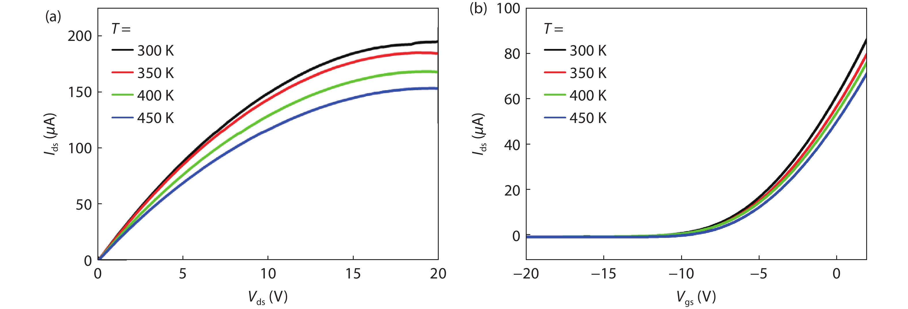
Black phosphorous (BP), an excellent two-dimensional (2D) monoelemental layered p-type semiconductor material with high carrier mobility and thickness-dependent tunable direct bandgap structure, has been widely applied in various devices. As the essential building blocks for modern electronic and optoelectronic devices, high quality PN junctions based on semiconductors have attracted widespread attention. Herein, we report a junction field-effect transistor (JFET) by integrating narrow-gap p-type BP and ultra-wide gap n-type β-Ga2O3 nanoflakes for the first time. BP and β-Ga2O3 form a vertical van der Waals (vdW) heterostructure by mechanically exfoliated method. The BP/β-Ga2O3 vdW heterostructure exhibits remarkable PN diode rectifying characteristics with a high rectifying ratio about 107 and a low reverse current around pA. More interestingly, by using the BP as the gate and β-Ga2O3 as the channel, the BP/β-Ga2O3 JFET devices demonstrate excellent n-channel JFET characteristics with the on/off ratio as high as 107, gate leakage current around as low as pA, maximum transconductance (gm) up to 25.3 µS and saturation drain current (IDSS) of 16.5 µA/µm. Moreover, it has a pinch-off voltage of –20 V and a minimum subthreshold swing of 260 mV/dec. These excellent n-channel JFET characteristics will expand the application of BP in future nanoelectronic devices.


J. Semicond.
2020, 41(8): 082003 doi: 10.1088/1674-4926/41/8/082003

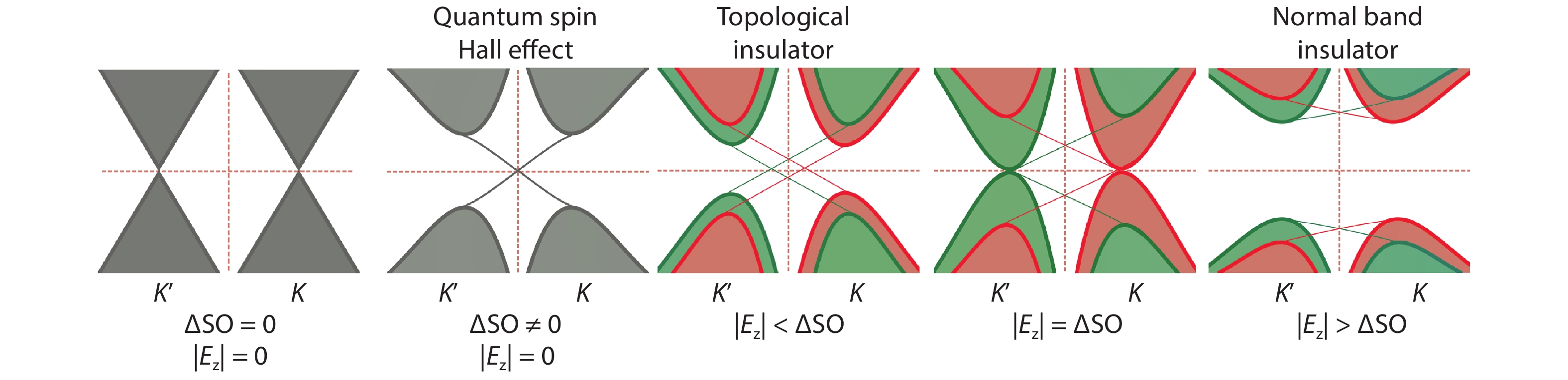
Germanene, the germanium analogue of graphene, shares many properties with its carbon counterpart. Both materials are two-dimensional materials that host Dirac fermions. There are, however, also a few important differences between these two materials: (1) graphene has a planar honeycomb lattice, whereas germanene’s honeycomb lattice is buckled and (2) the spin-orbit gap in germanene is predicted to be about three orders of magnitude larger than the spin-orbit gap in graphene (24 meV for germanene versus 20 μeV for graphene). Surprisingly, scanning tunneling spectra recorded on germanene layers synthesized on different substrates do not show any sign of the presence of a spin-orbit gap. To date the exact origin of the absence of this spin-orbit gap in the scanning tunneling spectra of germanene has remained a mystery. In this work we show that the absence of the spin-orbit gap can be explained by germanene’s exceptionally low work function of only 3.8 eV. The difference in work function between germanene and the scanning tunneling microscopy tip (the work functions of most commonly used STM tips are in the range of 4.5 to 5.5 eV) gives rise to an electric field in the tunnel junction. This electric field results in a strong suppression of the size of the spin-orbit gap.

J. Semicond.
2020, 41(8): 082004 doi: 10.1088/1674-4926/41/8/082004
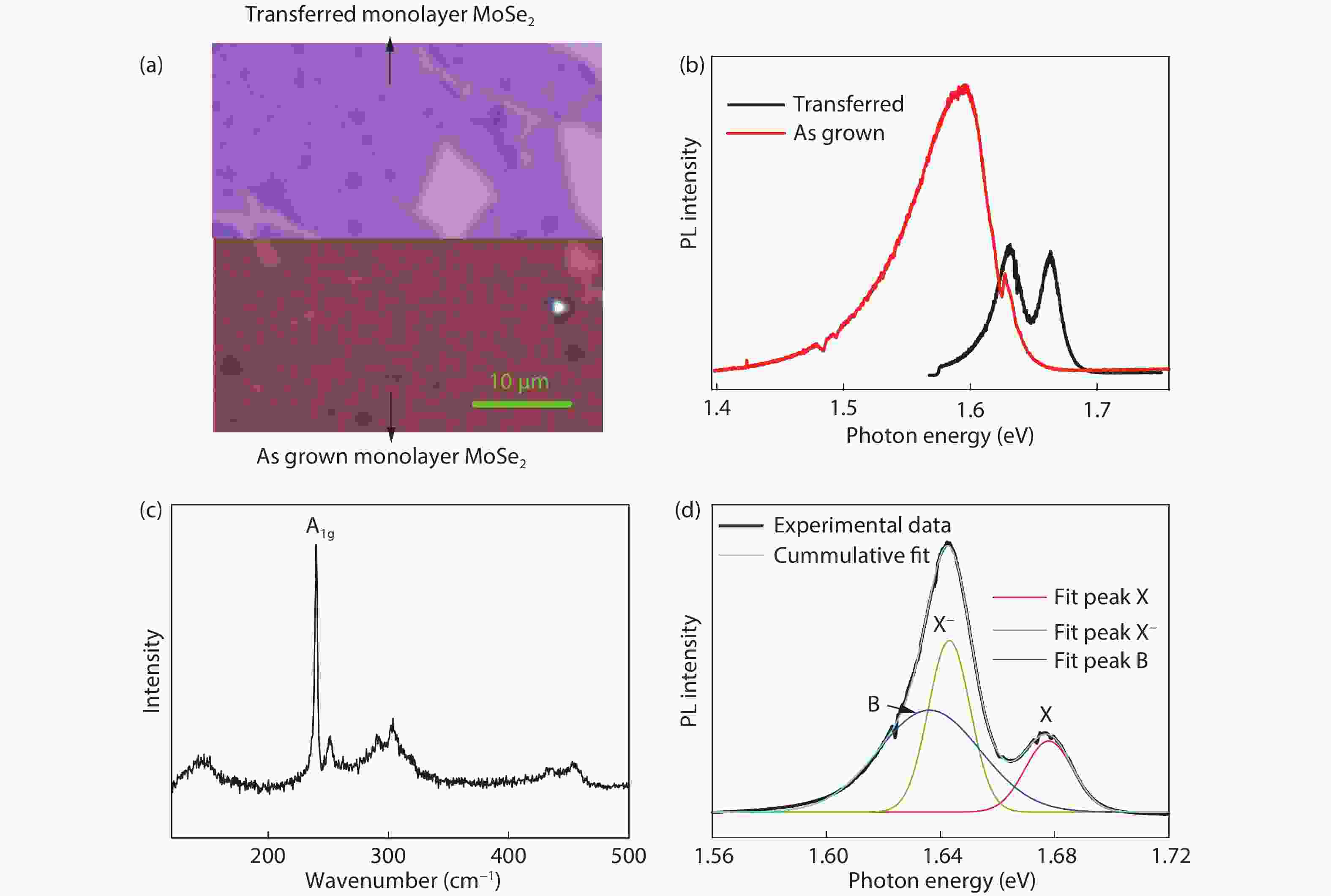
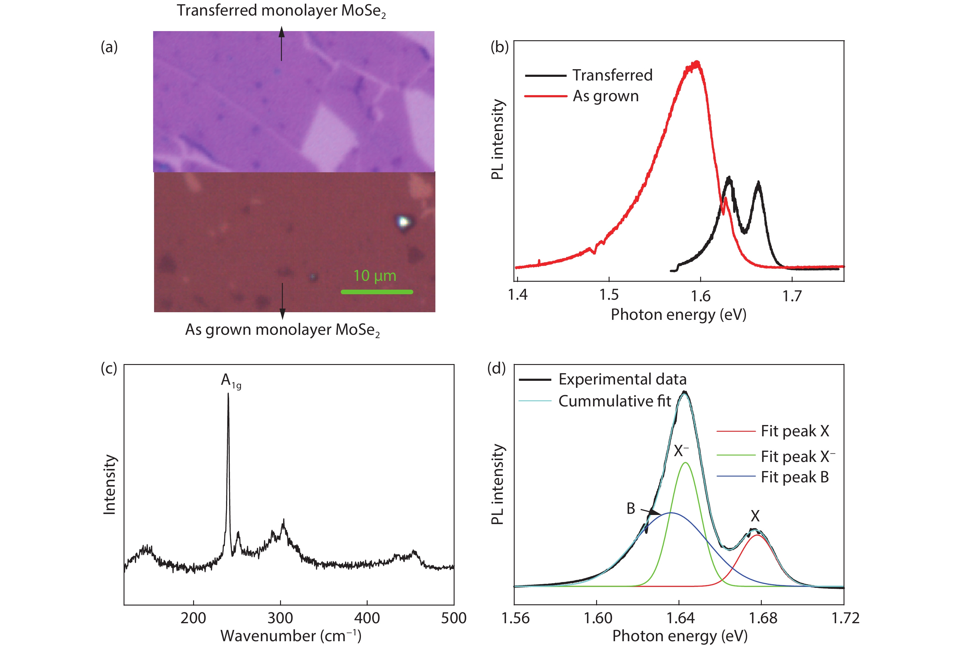
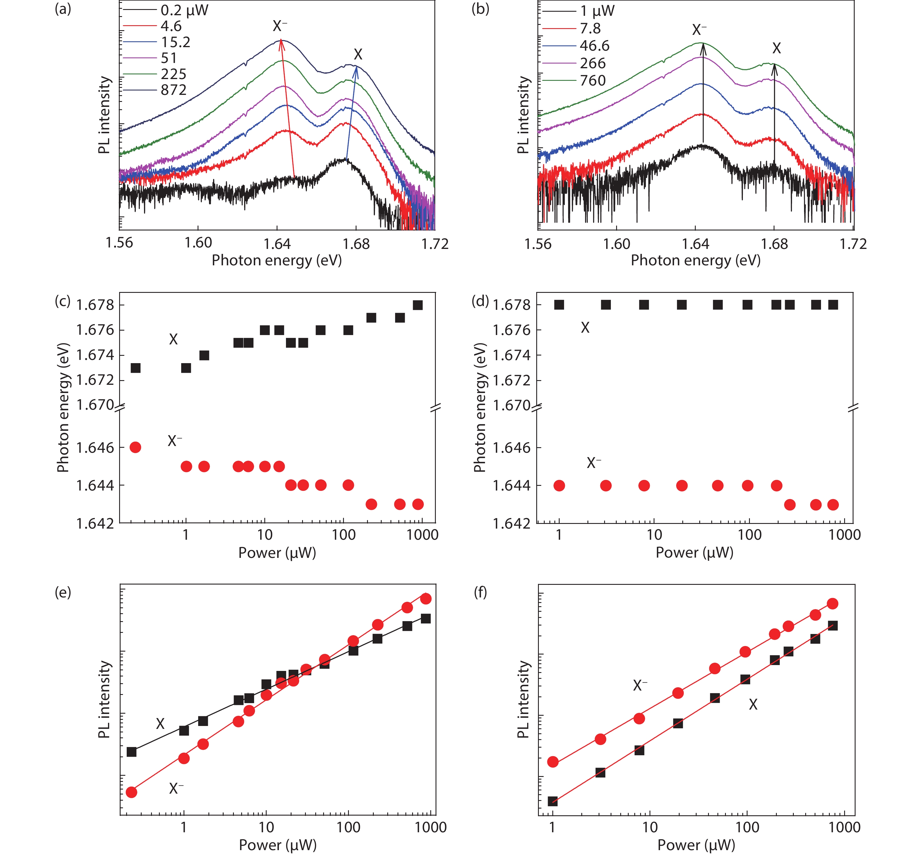
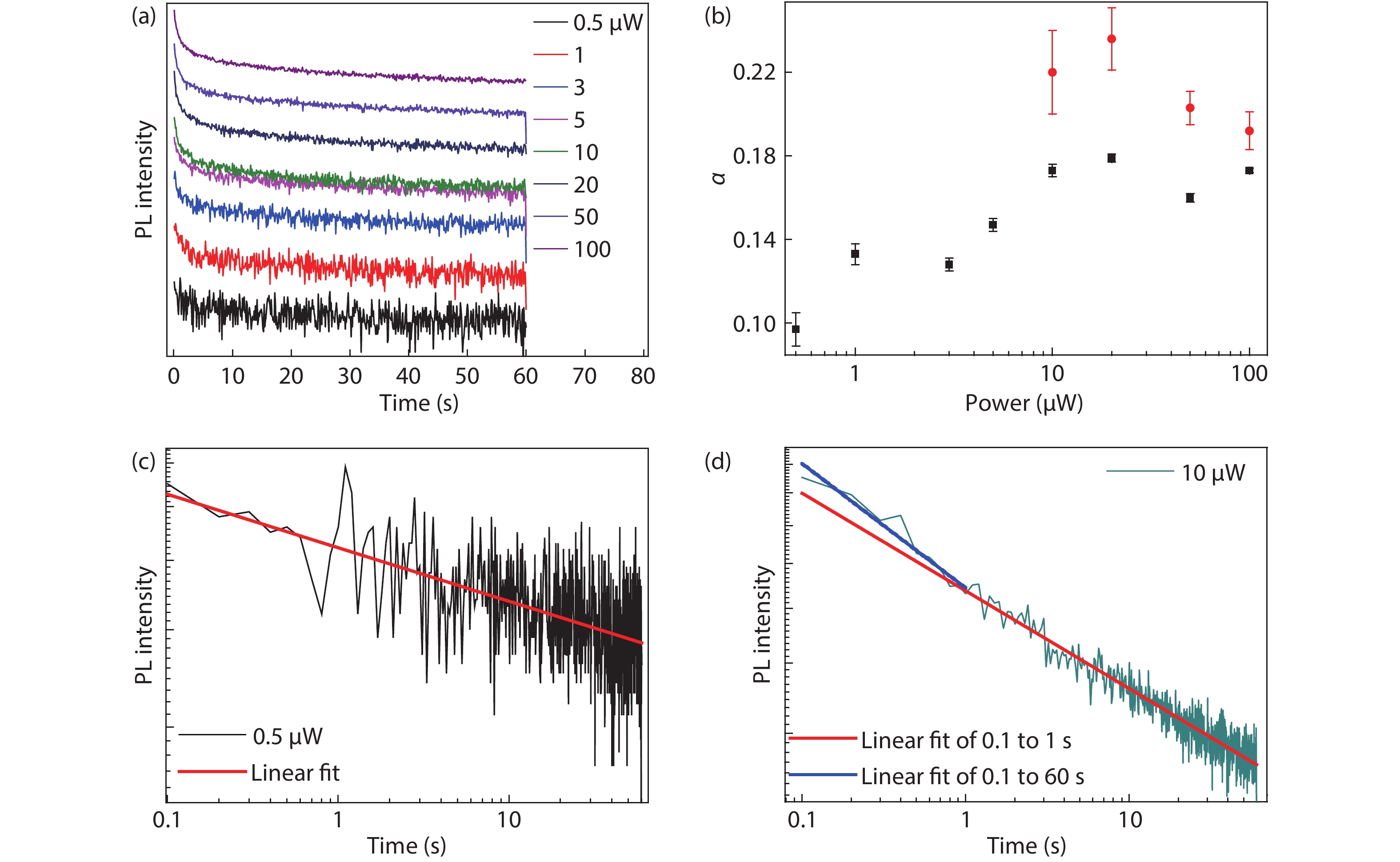
Dynamic processes of electron transfer by optical doping in monolayer MoSe2 at 6 K are investigated via measuring time resolved photoluminescence (PL) traces under different excitation powers. Time-dependent electron transfer process can be analyzed by a power-law distribution of t−α with α = 0.1–0.24, depending on the laser excitation power. The average electron transfer time of approximately 27.65 s is obtained in the excitation power range of 0.5 to 100 μW. As the temperature increases from 20 to 44 K, the energy difference between the neutral and charged excitons is observed to decrease.

J. Semicond.
2020, 41(8): 082005 doi: 10.1088/1674-4926/41/8/082005
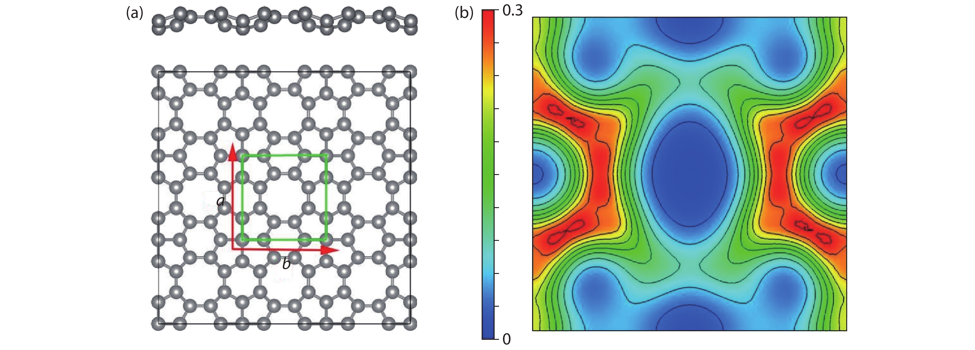
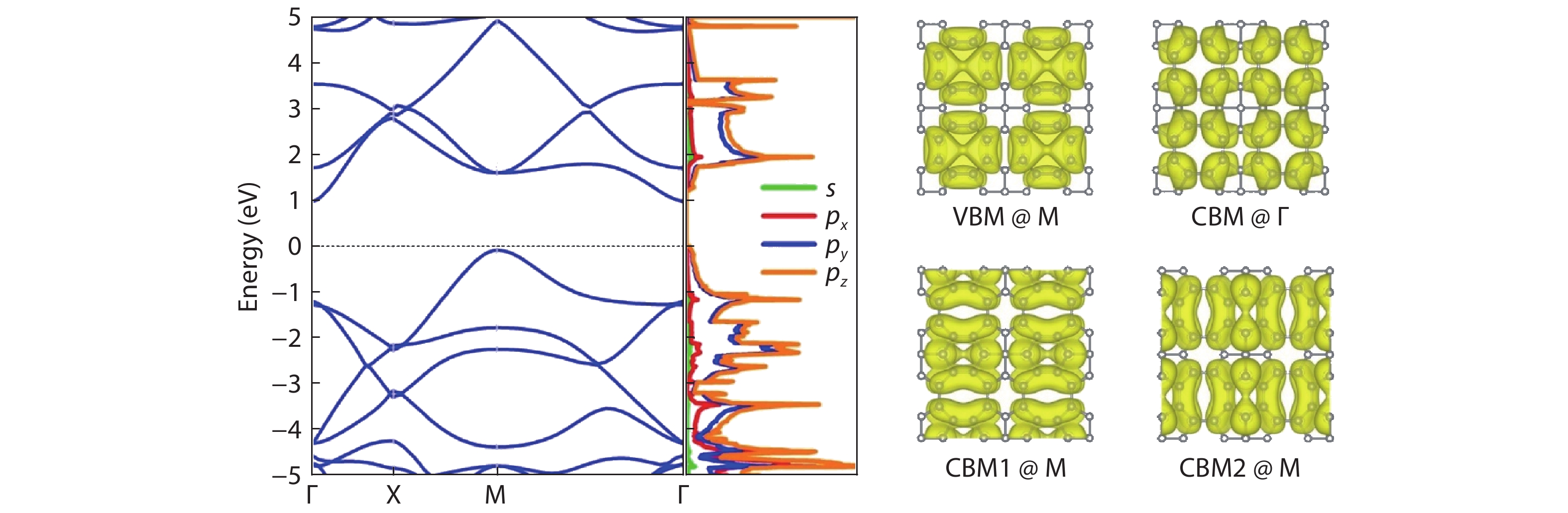
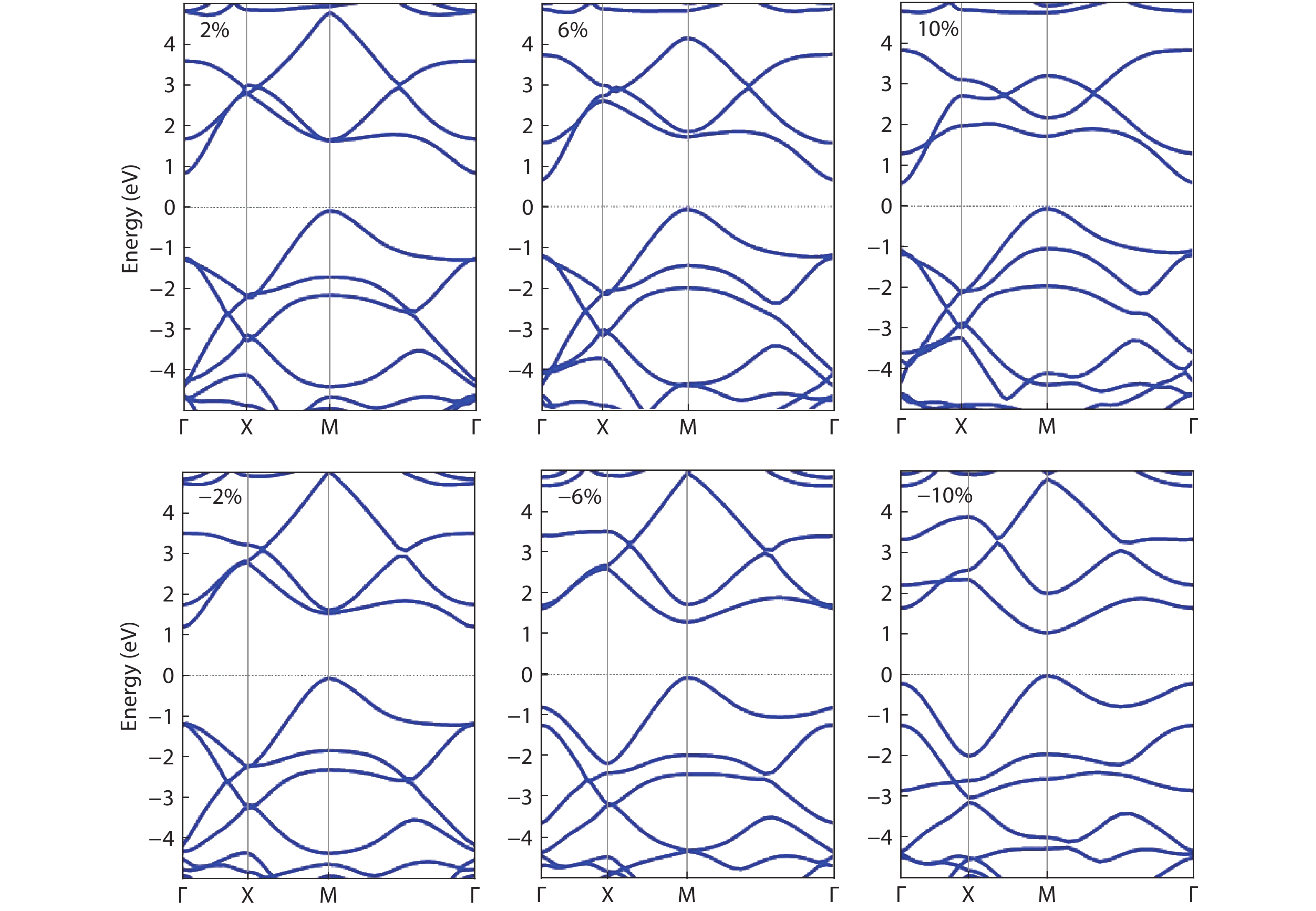
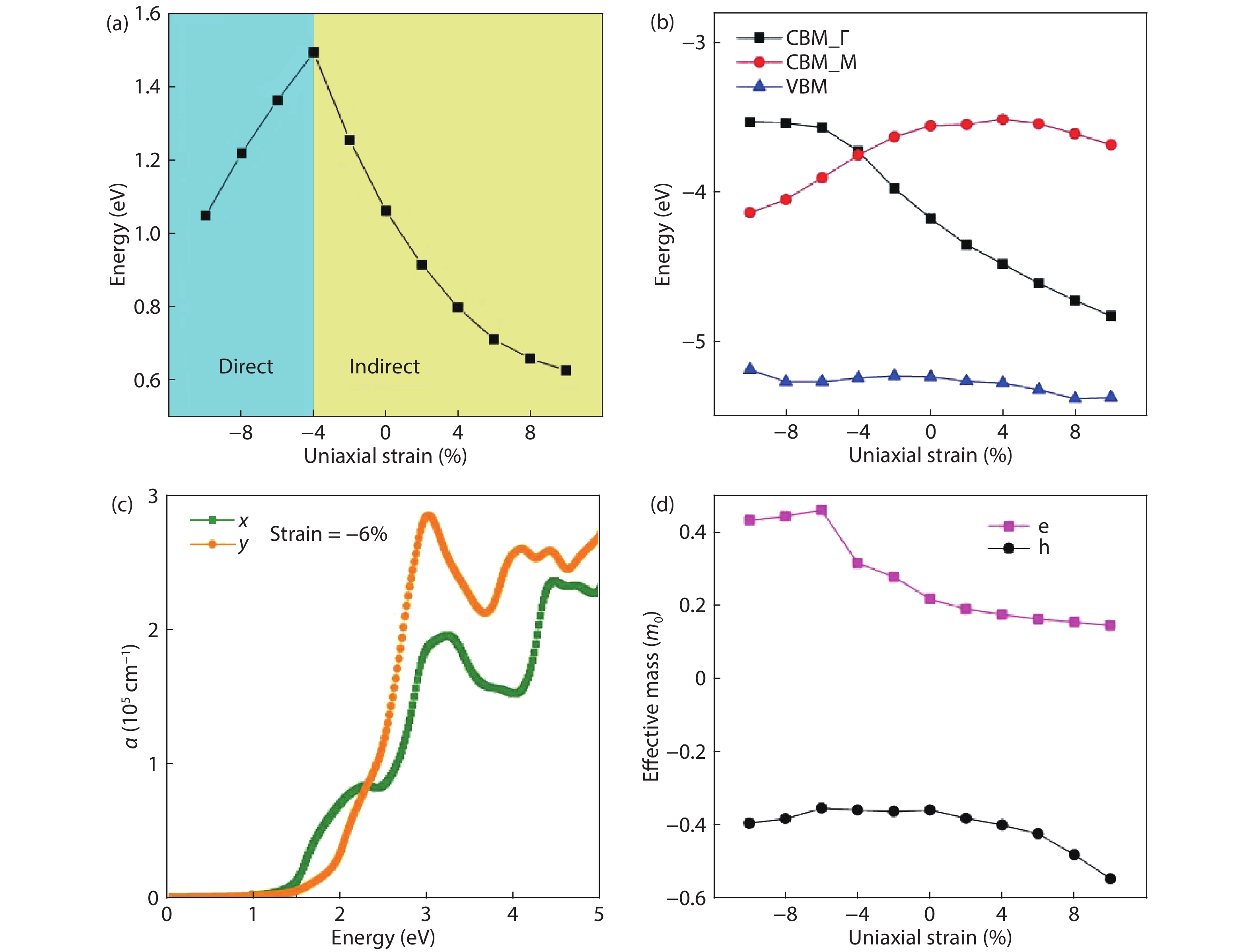
Recently, C568 has emerged as a new carbon allotrope, which shows semiconducting properties with a band gap around 1 eV and has attracted much attention. In this work, the external strain effects on the electronic properties of C568 have been studied theoretically through first-principle calculations. The numerical results show that while in-plane uniaxial and biaxial strains both reduces the band gap of C568 in case of tensile strain, their effects are quite different in the case of compressive strain. With increasing compressive uniaxial strain, the band gap of C568 first increases, and then dramatically decreases. In contrast, the application of compressive biaxial strain up to –10% only leads to a slight increase of band gap. Moreover, an indirect-to-direct gap transition can be realized under both types of compressive strain. The results also show that the optical anisotropy of C568 can be induced under uniaxial strain, while biaxial strain does not cause such an effect. These results indicate good strain tunability of the band structure of C568, which could be helpful for the design and optimization of C568-based nanodevices.


J. Semicond.
2020, 41(8): 082006 doi: 10.1088/1674-4926/41/8/082006

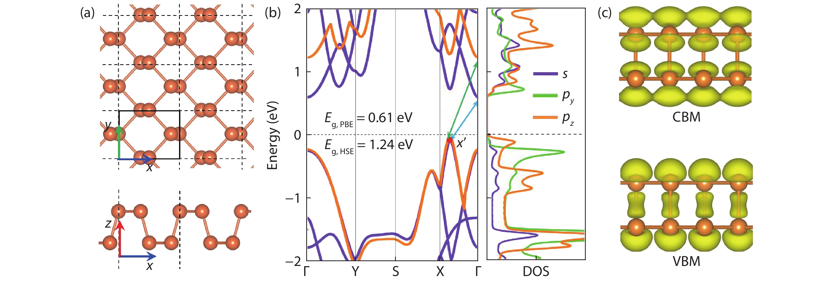
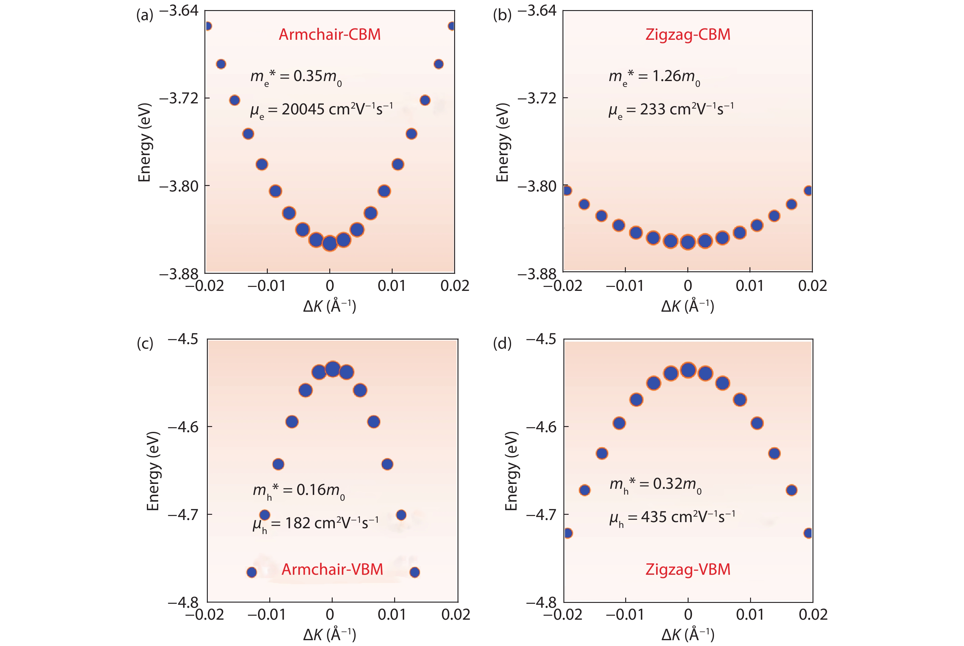
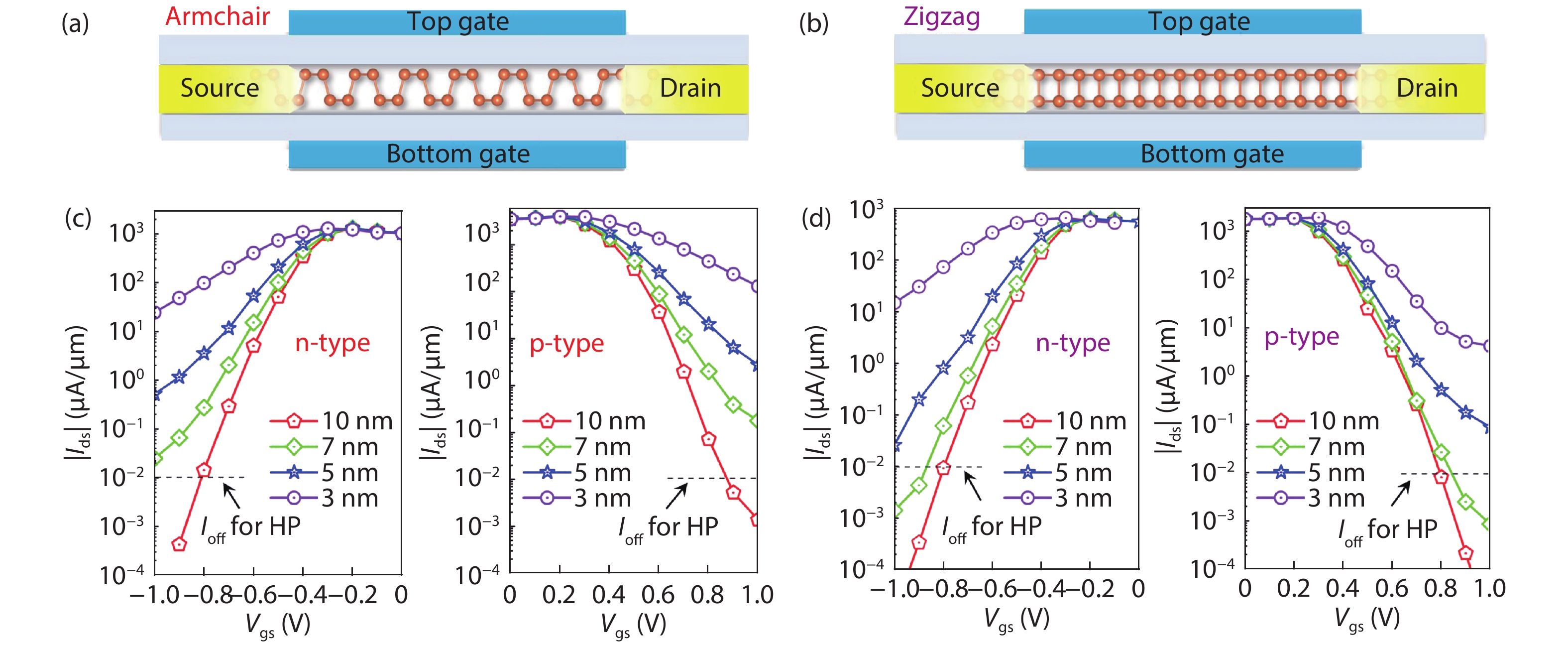
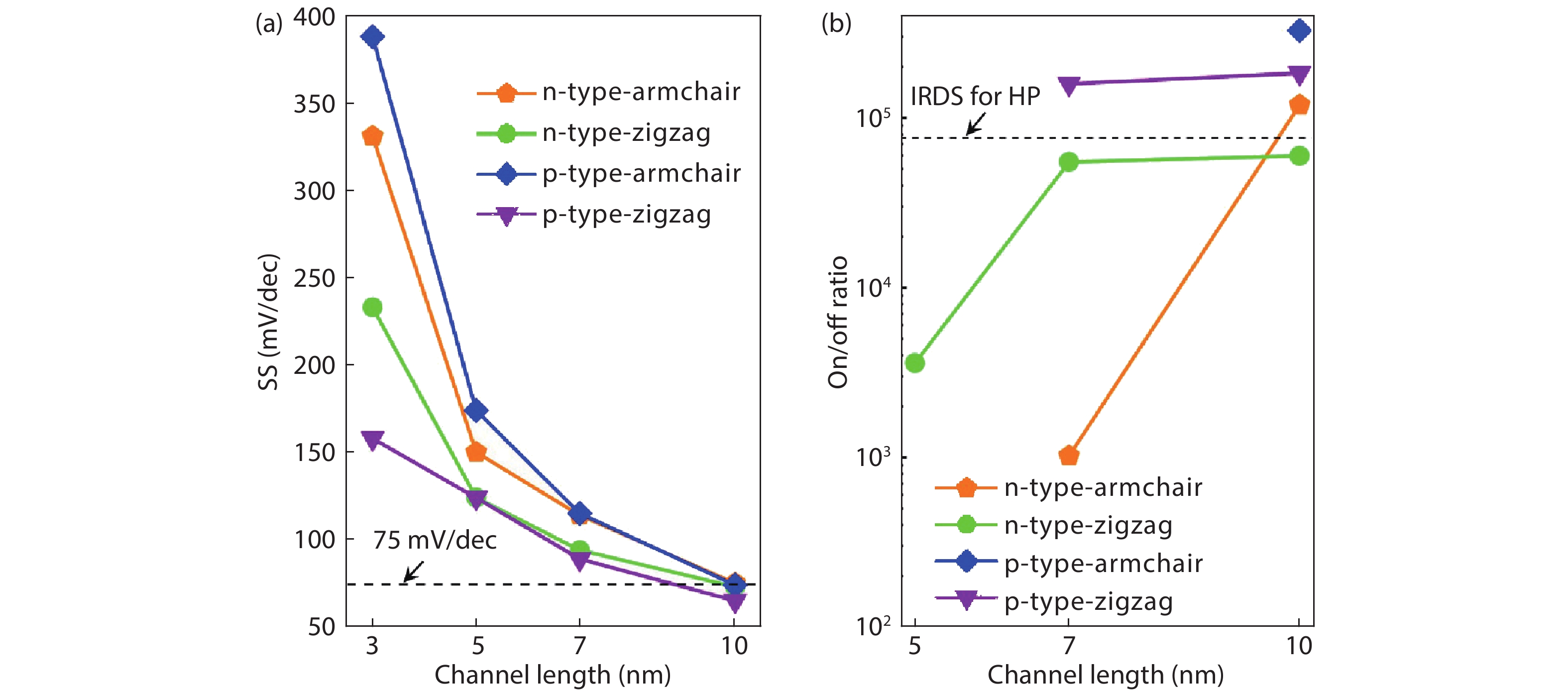
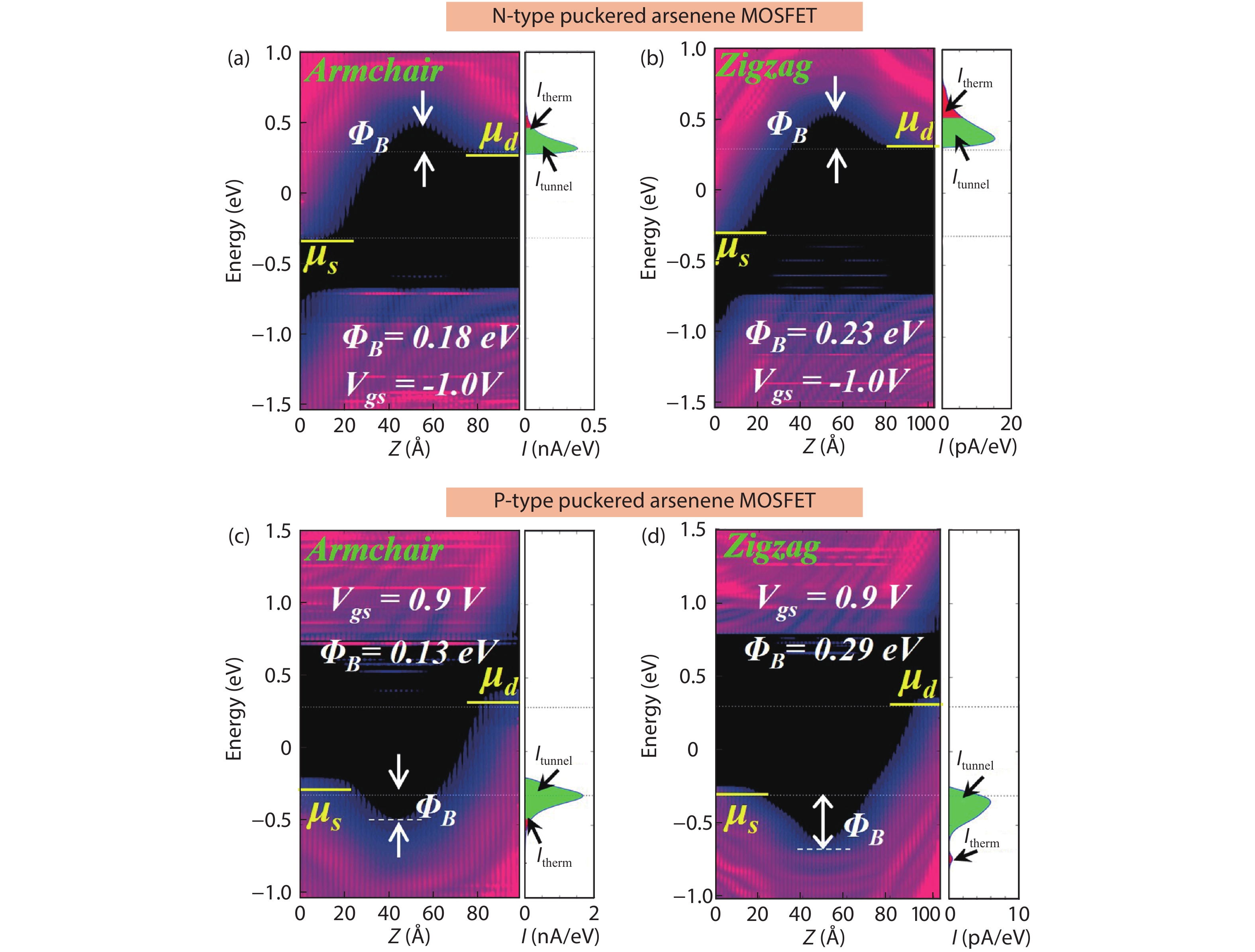
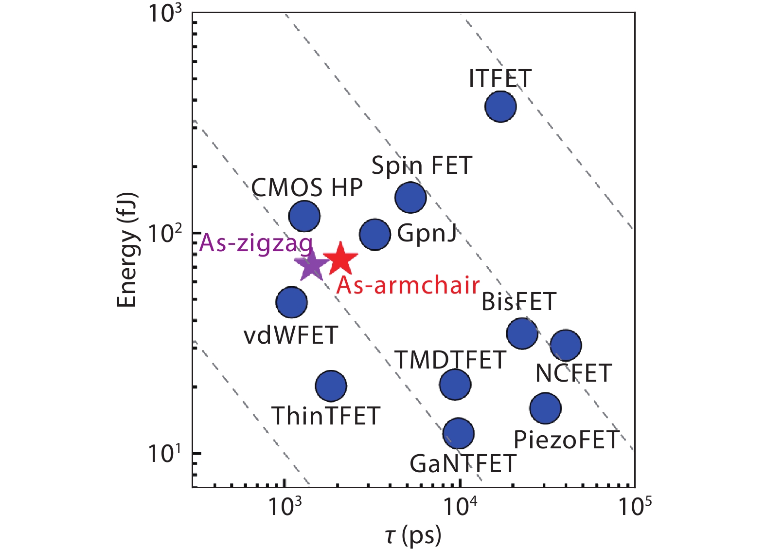
Two-dimensional material has been regarded as a competitive silicon-alternative with a gate length approaching sub-10 nm, due to its unique atomic thickness and outstanding electronic properties. Herein, we provide a comprehensively study on the electronic and ballistic transport properties of the puckered arsenene by the density functional theory coupled with nonequilibrium Green’s function formalism. The puckered arsenene exhibits an anisotropic characteristic, as effective mass for the electron/hole in the armchair and zigzag directions is 0.35/0.16 m0 and 1.26/0.32 m0. And it also holds a high electron mobility, as the highest value can reach 20 045 cm2V–1s–1. Moreover, the puckered arsenene FETs with a 10-nm channel length possess high on/off ratio above 105 and a steep subthreshold swing below 75 mV/dec, which have the potential to design high-performance electronic devices. Interestingly, the channel length limit for arsenene FETs can reach 7-nm. Furthermore, the benchmarking of the intrinsic arsenene FETs and the 32-bit arithmetic logic unit circuits also shows that the devices possess high switching speed and low energy dissipation, which can be comparable to the CMOS technologies and other CMOS alternatives. Therefore, the puckered arsenene is an attractive channel material in next-generation electronics.