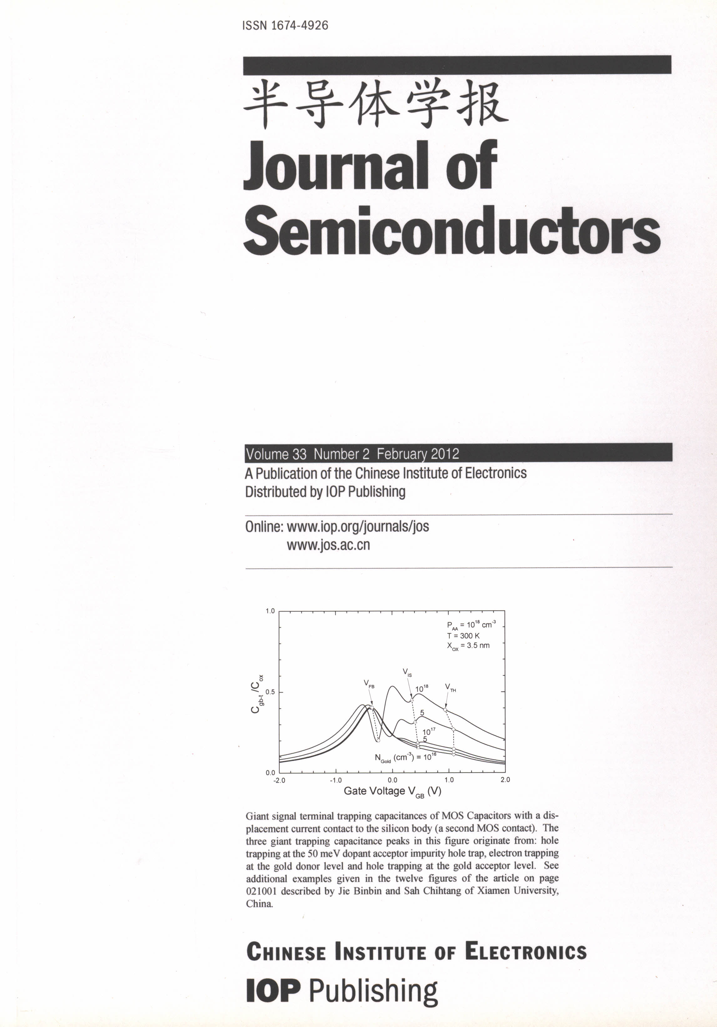
Low-frequency and High-frequency Capacitance-Voltage (C-V) curves of Silicon Metal-Oxide-linebreak Semiconductor Capacitors, showing electron and hole trapping at shallow-level dopant and deep-level generation-recombination-trapping impurities, are presented to illustrate the enhancement of the giant trapping capacitances by physical means via device and circuit designs, in contrast to chemical means via impurity characteristics previously reported. Enhancement is realized by masking the electron or/and hole storage capacitances to make the trapping capacitances dominant at the terminals. Device and materials properties used in the computed CV curves are selected to illustrate experimental realizations for fundamental trapping parameter characterizations and for electrical and optical signal processing applications.
Device characteristics of TiO2 gate dielectrics deposited by a sol-gel method and DC sputtering method on a P-type silicon wafer are reported. Metal-oxide-semiconductor capacitors with Al as the top electrode were fabricated to study the electrical properties of TiO2 films. The films were physically characterized by using X-ray diffraction, a capacitor voltage measurement, scanning electron microscopy, and by spectroscopy ellipsometry. The XRD and DST-TG indicate the presence of an anatase TiO2 phase in the film. Films deposited at higher temperatures showed better crystallinity. The dielectric constant calculated using the capacitance voltage measurement was found to be 18 and 73 for sputtering and sol-gel samples respectively. The refractive indices of the films were found to be 2.16 for sputtering and 2.42 for sol-gel samples.
Sn/Cu/ZnS precursor were deposited by evaporation on soda lime glass at room temperature, and then polycrystalline thin films of Cu2ZnSnS4 (CZTS) were produced by sulfurizing the precursors in a sulfur atmosphere at a temperature of 550 ℃ for 3 h. Fabricated CZTS thin films were characterized by X-ray diffraction, energy dispersive X-ray spectroscopy, ultraviolet-visible-near infrared spectrophotometry, the Hall effect system, and 3D optical microscopy. The experimental results show that, when the ratios of [Cu]/([Zn] + [Sn]) and [Zn]/[Sn] in the CZTS are 0.83 and 1.15, the CZTS thin films possess an absorption coefficient of larger than 4.0 × 104 cm-1 in the energy range 1.5-3.5 eV, and a direct band gap of about 1.47 eV. The carrier concentration, resistivity and mobility of the CZTS film are 6.98 × 1016 cm-3, 6.96 Ω·cm, and 12.9 cm2/(V.s), respectively and the conduction type is p-type. Therefore, the CZTS thin films are suitable for absorption layers of solar cells.
Patterned ZnO nanowires were successfully synthesized on ITO electrodes deposited on the glass substrate by using a simple thermal evaporation approach. The morphology, crystallinity and optical properties of ZnO nanowires were characterized by scanning electron microscopy, X-ray diffraction, energy dispersive X-ray and photoluminescence spectroscopy. Their field emission characteristics were also investigated. SEM images showed that the ZnO nanowires, with a diameter of 100-200 nm and length up to 5 μm, were highly uniform and well distributed on the linear ITO electrodes. The field emission measurement indicated that patterned ZnO nanowire arrays have a turn-on field of 1.6 V/μm at current density of 1 μ A/cm2 and a threshold field of 4.92 V/μ m at current density of 1 mA/cm2 at an emitter-anode gap of 700 μm. The current density rapidly reached 2.26 mA/cm2 at an applied field of 5.38 V/μm. The fluctuation of emission current was lower than 5% for 4.5 h. The low turn-on field, high current density and good stability of patterned ZnO nanowire arrays indicate that it is a promising candidate for field emission application.
The application of a p+/p configuration in the window layer of hydrogenated amorphous silicon thin film solar cells is simulated and analyzed utilizing an AMPS-1D program. The differences between p+-p-i-n configuration solar cells and p-i-n configuration solar cells are pointed out. The effects of dopant concentration, thickness of p+-layer, contact barrier height and defect density on solar cells are analyzed. Our results indicate that solar cells with a p+-p-i-n configuration have a better performance. The open circuit voltage and short circuit current were improved by increasing the dopant concentration of the p+ layer and lowering the front contact barrier height. The defect density at the p/i interface which exceeds two orders of magnitude in the intrinsic layer will deteriorate the cell property.
A new 2D analytical drain current model is presented for symmetric double-gate fully depleted nanoscale SOI MOSFETs. Investigation of device parameters like transconductance for double-gate fully depleted nanoscale SOI MOSFETs is also carried out. Finally this work is concluded by modeling the cut-off frequency, which is one of the main figures of merit for analog/RF performance for double-gate fully depleted nanoscale SOI MOSFETs. The results of the modeling are compared with those obtained by a 2D ATLAS device simulator to verify the accuracy of the proposed model.
The performance of a LOCOS-isolated SOI MOSFET heavily depends on its back-gate characteristic, which can be affected by back-gate stress. A large voltage stress was applied to the back gate of SOI devices for at least 30 s at room temperature, which could effectively modify the back-gate threshold voltage of these devices. This modification is stable and time invariant. In order to improve the back-gate threshold voltage, positive substrate bias was applied to NMOS devices and negative substrate bias was applied to PMOS devices. These results suggest that there is a leakage path between source and drain along the silicon island edge, and the application of large back-gate bias with the source, drain and gate grounded can strongly affect this leakage path. So we draw the conclusion that the back-gate threshold voltage, which is directly related to the leakage current, can be influenced by back-gate stress.
The anode injection efficiency reduction of 3.3-kV-class non-punch-through insulated-gate bipolar transistors (NPT-IGBTs) due to backside processes is experimentally studied through comparing the forward blocking capabilities of the experiments and the theoretical breakdown model in this paper. Wafer lifetimes are measured by a μ-PCD method, and well designed NPT-IGBTs with a final wafer thickness of 500 μm are fabricated. The test results show higher breakdown voltages than the theoretical breakdown model in which anode injection efficiency reduction is not considered. This indicates that anode injection efficiency reduction must be considered in the breakdown model. Furthermore, the parameters related to anode injection efficiency reduction are estimated according to the experimental data.
Isolated extended drain NMOS (EDNMOS) transistors are widely used in power signal processing. The hole current induced by a high electric field can result in a serious reliability problem due to a parasitic NPN effect. By optimizing p-type epitaxial (p-epi) thickness, n-type buried layer (BLN) and nwell doping distribution, the peak electric field is decreased by 30% and the peak hole current is decreased by 60%, which obviously suppress the parasitic NPN effect. Measured I-V characteristics and transmission line pulsing (TLP) results show that the on-state breakdown voltage is increased from 28 to 37 V when 6 V VMgs is applied and the energy capability is improved by about 30%, while the on-state resistance remains unchanged.
Distributed feedback (DFB) quantum cascade lasers (QCLs) in continuous-wave (CW) mode emitting at λ ≈ 7.6 μm are presented. Holographic lithography was used to fabricate the first-order distributed feedback grating. For a high-reflectivity-coated QCL with 14.5-μm-wide and 3-mm-long cavity, CW output powers of 300 mW at 85 K and still 10 mW at 270 K are obtained. Single-mode emission with a side-mode suppression ratio (SMSR) of about 30 dB and a wide tuning range of ~300 nm in the temperature range from 85 to 280 K is observed.
GaInP/GaAs/Ge tandem solar cells were fabricated by a MOCVD technique. The photoelectric properties of the solar cells were characterized by a current-voltage test method. The dependence of the solar cell's characteristics on temperature were investigated from 30 to 170 ℃ at intervals of 20 ℃. Test results indicated that with increasing temperature, Jsc of the cell increased slightly with a temperature coefficient of 9.8 (μA/cm2)/℃. Voc reduced sharply with a coefficient of -5.6 mV/℃. FF was reduced with a temperature coefficient of -0.00063/℃. Furthermore, the conversion efficiency decreased linearly with increasing temperature which decreased from 28% at 30 ℃ to 22.1% at 130 ℃. Also, detailed theoretical analyses for temperature characteristics of the solar cell were given.
This paper discusses the design of a wideband low noise amplifier (LNA) in which specific architecture decisions were made in consideration of system-on-chip implementation for radio-astronomy applications. The LNA design is based on a novel ultra-low noise InGaAs/InAlAs/InP pHEMT. Linear and non-linear modelling of this pHEMT has been used to design an LNA operating from 2 to 4 GHz. A common-drain in cascade with a common source inductive degeneration, broadband LNA topology is proposed for wideband applications. The proposed configuration achieved a maximum gain of 27 dB and a noise figure of 0.3 dB with a good input and output return loss (S11 < -10 dB, S22 < -11 dB). This LNA exhibits an input 1-dB compression point of -18 dBm, a third order input intercept point of 0 dBm and consumes 85 mW of power from a 1.8 V supply.
A generally improved recycling folded cascode (IRFC) is analyzed and implemented. Analysis and comparisons among the IRFC, the original recycling folded cascode (RFC) and the conventional folded cascode (FC) are made, and it is shown that with the flexible structure of IRFC, significant enhancement in transconductance, slew rate and noise can be achieved. Prototype amplifiers were fabricated in 0.13 μm technology. Measurement shows that IRFC has 3× enhancement in gain-bandwidth and slew rate over conventional FC, and the enhancement is 1.5× when compared with the RFC.
This paper designs a binary-weighted programmable gain amplifier (PGA) with a DC offset cancellation (DCOC) circuit and an AB-class output buffer. The PGA adopts the circuit topology of a differential amplifier with diode-connected loads. Simulation shows that the performance of the PGA is not sensitive to temperature and process variation. According to test results, controlled by a digital signal of six bits, the PGA can realize a dynamic gain of -2 to 61 dB, and a gain step of 1 dB with a step error within ± 0.38 dB. The minimum 3 dB bandwidth is 92 MHz. At low-gain mode, IIP3 is 17 dBm, and a 1 dB compression point can reach 5.7 dBm. The DCOC circuit enables the amplifier to be used in a direct-conversion receiver and the AB-class output buffer circuit reduces the overall static power consumption.
This paper presents a broadband Gilbert low noise mixer implemented with noise cancellation technique operating between 10 MHz and 0.9 GHz. The Gilbert mixer is known for its perfect port isolation and bad noise performance. The noise cancellation technique of LNA can be applied here to have a better NF. The chip is implemented in SMIC 0.18 μm CMOS technology. Measurement shows that the proposed low noise mixer has a 13.7-19.5 dB voltage gain from 10 MHz to 0.9 GHz, an average noise figure of 5 dB and a minimum value of 4.3 dB. The core area is 0.6 × 0.45 mm2.
This paper introduces a low-noise low-cost ΣΔ modulator for digital audio analog-to-digital conversion. By adopting a low-noise large-output swing operation amplifier, not only is the flicker noise greatly inhibited, but also the power consumption is reduced. Also the area cost is relatively small. The modulator was implemented in a SMIC standard 65-nm CMOS process. Measurement results show it can achieve 96 dB peak signal-to-noise plus distortion ratio (SNDR) and 105 dB dynamic range (DR) over the 22.05-kHz audio band and occupies 0.16 mm2. The power consumption of the proposed modulator is 4.9 mW from a 2.5 V power supply, which is suitable for high-performance, low-cost audio codec applications.
This paper presents a first monolithic RF transceiver for DC-OFDM UWB applications. The proposed direct-conversion transceiver integrates all the building blocks including two receiver (Rx) cores, two transmitter (Tx) cores and a dual-carrier frequency synthesizer (DC-FS) as well as a 3-wire serial peripheral interface (SPI) to set the operating status of the transceiver. The ESD-protected chip is fabricated by a TSMC 0.13-μm RF CMOS process with a die size of 4.5 × 3.6 mm2. The measurement results show that the wideband Rx achieves an NF of 5-6.2 dB, a max gain of 76-84 dB with 64-dB variable gain, an in-/out-of-band IIP3 of -6/+4 dBm and an input loss S_11 of < -10 in all bands. The Tx achieves an LOLRR/IMGRR of -34/-33 dBc, a typical OIP3 of +6 dBm and a maximum output power of -5 dBm. The DC-FS outputs two separate carriers simultaneously with an inter-band hopping time of < 1.2 ns. The full chip consumes a maximum current of 420 mA under a 1.2-V supply.
A fully integrated receiver RF front-end that meets WCDMA/GSM system requirements is presented. It supports SAW-less operation for WCDMA. To improve the linearity in terms of both IP3 and IP2, the RF front-end is comprised of multiple-gated LNAs with capacitive desensitization, current-mode passive mixers with the proposed IP2 calibration circuit and reconfigurable Tow-Thomas-like biquad TIAs. A new power-saving multi-mode divider with low phase noise is proposed to provide the 4-phase 25%-duty-cycle LO. In addition, a constant-gm biasing with an on-chip resistor is adopted to make the conversion gain invulnerable to the process and temperature variations of the transimpedance. This RF front-end is integrated in a receiver with an on-chip frequency synthesizer in 0.13 m CMOS. The measurement results show that owing to this high-linearity RF front-end, the receiver achieves ??6 dBm IIP3 and better than +60 dBm IIP2 for all modes and bands.
A wideband LC-tuned voltage-controlled oscillator (LC-VCO) applied in LTE PLL frequency synthesizers with constant KVCO/ωosc is described. In order to minimize the loop bandwidth variations of PLL, a varactor array is proposed, which consists of a series of differential variable capacitor pairs and a series of single-pole double-throw (SPDT) switches to connect Vtune or VDD. The switches are controlled by switching bits. With this scheme, the ratio of KV= ∂ Cvar/∂ Vtune and the capacitance value of the capacitor array maintains relatively constant; furthermore, the loop bandwidth of the PLL fluctuation is suppressed. The 3.2-4.6-GHz VCO for multi-band LTE PLL is fabricated in a 0.13-μ m RF-CMOS process. The VCO exhibits a maximum variation of KVCO/ωosc of only ±4%. The VCO also exhibits a low phase-noise of -124 dBc/Hz at a 1-MHz offset frequency and a low current consumption of 18.0 mA with a 1.2-V power supply.
An output amplitude configurable wideband automatic gain control (AGC) with high gain step accuracy for the GNSS receiver is presented. The amplitude of an AGC is configurable in order to cooperate with baseband chips to achieve interference suppression and be compatible with different full range ADCs. And what's more, the gain-boosting technology is introduced and the circuit is improved to increase the step accuracy. A zero, which is composed by the source feedback resistance and the source capacity, is introduced to compensate for the pole. The AGC is fabricated in a 0.18 μm CMOS process. The AGC shows a 62 dB gain control range by 1 dB each step with a gain error of less than 0.2 dB. The AGC provides 3 dB bandwidth larger than 80 MHz and the overall power consumption is less than 1.8 mA, and the die area is 800 × 300 μm2.
A new design technique for merging the front-end sample-and-hold amplifier (SHA) into the first multiplying digital-to-analog converter (MDAC) is presented. For reducing the aperture error in the first stage of the pipelined ADC, a symmetrical structure is used in a flash ADC and MDAC. Furthermore, a variable resistor tuning network is placed at the flash input to compensate for different cutoff frequencies of the input impedances of the flash and MDAC. The circuit also has a clear clock phase in the MDAC and separate sampling capacitors in the flash ADC to eliminate the nonlinear charge kickback to the input signal. The proposed circuit, designed using ASMC 0.35-μm BiCMOS technology, occupies an area of 1.4 × 9 mm2 and is used as the front-end stage in a 14-bit 125-MS/s pipelined ADC. After the trim circuit is enabled, the measured signal-to-noise ratio is improved from 71.5 to 73.6 dB and the spurious free dynamic range is improved from 80.5 to 83.1 dB with a 30.8 MHz input. The maximum input frequency is up to 150 MHz without steep performance degradations.
We report a high-speed flash analog to digital converter (ADC) linearization technique employing the inverse Volterra model and digital post processing. First, a 1.25 GS/s 5-bit flash ADC is designed using a 0.18 μm CMOS, and the signal is quantized by a distributed track-and-hold circuit. Second, based on the Volterra series, a proposed digital post-calibration model is introduced. Then, the model is applied to estimate and compensate the nonlinearity of the high-speed flash ADC. Simulation results indicate that the distortion is reduced effectively. Specifically, the ADC achieves gains of 4.83 effective bits for a 117.1 MHz frequency input and 4.74 effective bits for a Nyquist input at 1.25 GS/s.
This paper presents a design of 14-bit 80 Msample/s pipelined ADC implemented in 0.35 μm CMOS. A charge-sharing correction is proposed to remove the signal-dependent charge-injection, together with a low-jitter clock circuit, guaranteeing the high dynamic performance for the ADC. A scheme of capacitor-switching and a symmetrical layout technique minimizes capacitor mismatch, ensuring the overall linearity. The measured results show that the calibration-free ADC achieves an effective number of bits of 11.6-bit, spurious free dynamic range (SFDR) of 84.8 dB, signal-to-noise-and-distortion ratio (SNDR) of 72 dB, differential nonlinearity of +0.63/-0.6 LSB and integrated nonlinearity of +1.3/-0.9 LSB at 36.7 MHz input and maintains over 75 dB SFDR and 59 dB SNDR up to 200 MHz.
This paper describes the design and test of a novel custom driving circuit for multi-quantum-well (MQW) spatial light modulators (SLMs). Unlike previous solutions, we integrated all blocks in one chip to synchronize the control logic circuit and the driving circuits. Single-slope digital-to-analog converters (DACs) inside each pixel are not adopted because it is difficult to eliminate capacitor mismatch. 64 column-shared 8-bit resistor-string DACs are utilized to provide programmable output voltages from 0.5 to 3.8 V. They are located on the top of 64 × 64 driving pixels tightly to match each other with several dummies. Each DAC performs its conversion in 280 ns and draws 80 μA. For a high speed data transfer rate, the system adopts a 2-stage shift register that operates at 50 MHz and the modulating rate achieves 50 K frames/s while dissipating 302 mW from a 5-V supply. The die is fabricated in a 0.35 μm CMOS process and its area is 5.5 × 7 mm2.
A third-order, sub-1 V bandgap voltage reference design for low-power supply, high-precision applications is presented. This design uses a current-mode compensation technique and temperature-dependent resistor ratio to obtain high-order curvature compensation. The circuit was designed and fabricated by SMIC 0.18 μm CMOS technology. It produces an output reference of 713.6 mV. The temperature coefficient is 3.235 ppm/℃ in the temperature range of -40 to 120 ℃, with a line regulation of 0.199 mV/V when the supply voltage varies from 0.95 to 3 V. The average current consumption of the whole circuit is 49 μA at the supply voltage of 1 V.
This paper presents a method of designing a 65 nm DFM standard cell library. By reducing the amount of the library largely, the process of optical proximity correction (OPC) becomes more efficient and the need for large storage is reduced. This library is more manufacture-friendly as each cell has been optimized according to the DFM rule and optical simulation. The area penalty is minor compared with traditional library, and the timing, as well as power has a good performance. Furthermore, this library has passed the test from the Technology Design Department of Foundry. The result shows this DFM standard cell library has advantages that improve the yield.
Highly controllable ICP etching of GaAs based materials with SiCl4/Ar plasma is investigated. A slow etching rate of 13 nm/min was achieved with RF1 = 10 W, RF2 = 20 W and a high ratio of Ar to SiCl4 flow. First order gratings with 25 nm depth and 140 nm period were fabricated with the optimal parameters. AFM analysis indicated that the RMS roughness over a 10 × 10 μm2 area was 0.3 nm, which is smooth enough to regrow high quality materials for devices.
首先强调了2012 年国家自然科学基金的一些新变化,如面上项目平均资助强度将会继续提升至80万元/4 年、新增了优秀青年科学基金以及在当年结题的青年科学基金项目中择优遴选5% 给予面上项目连续资助。然后倡导大家关注器件制备和基础工艺中的关键科学问题,力争将基础研究工作做扎实做深入。最后分析介绍了2011 年半导体科学和信息器件学科组面上、青年、地区和重点基金申请与资助概况,供大家参考。