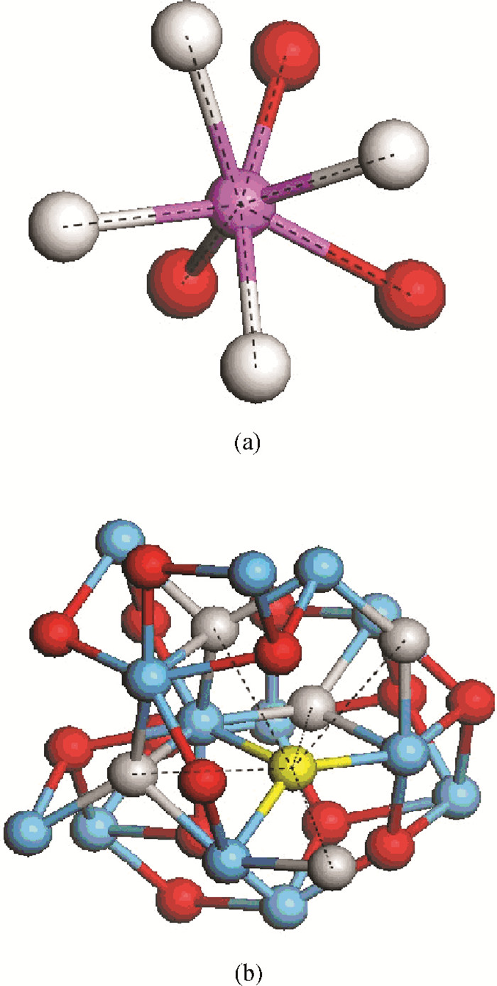
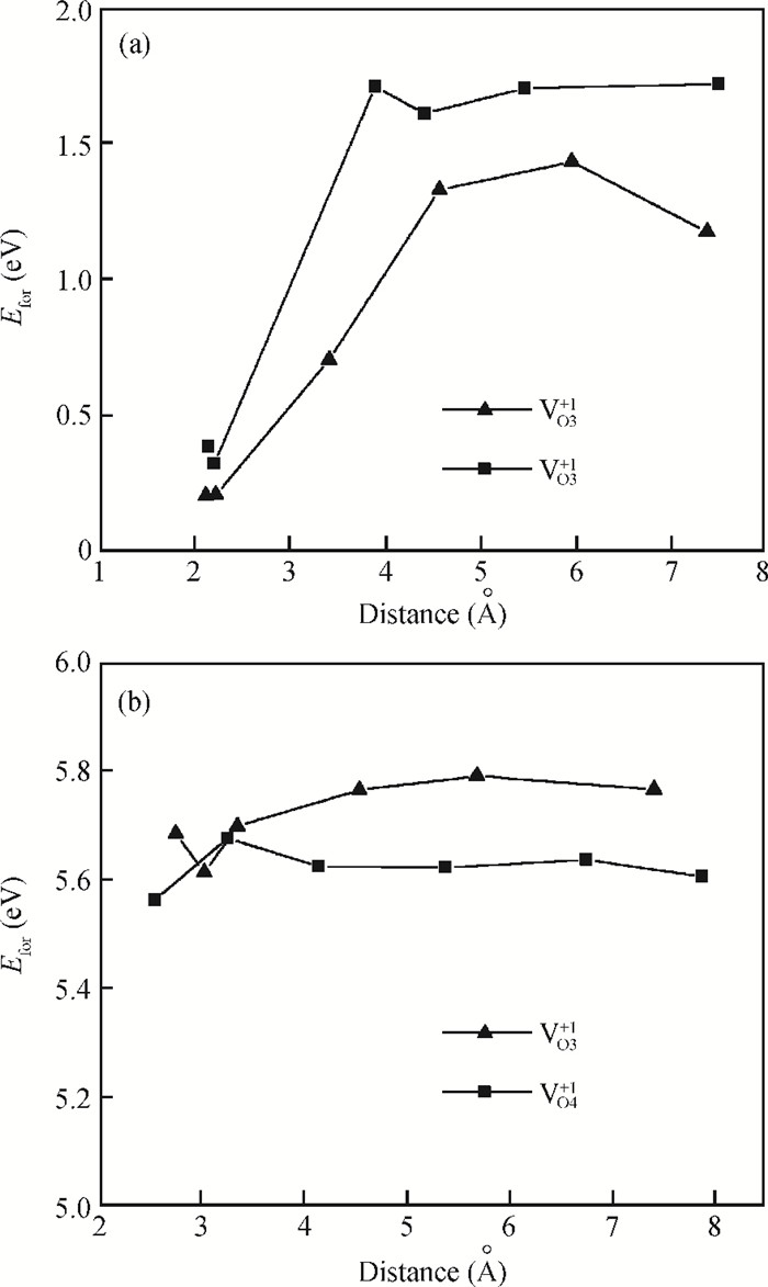
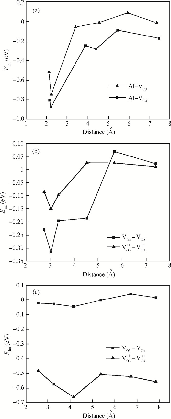
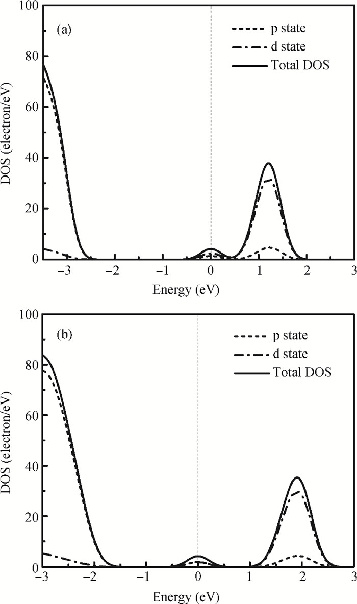
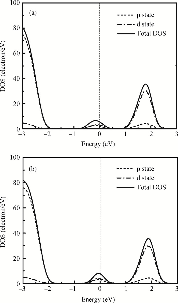
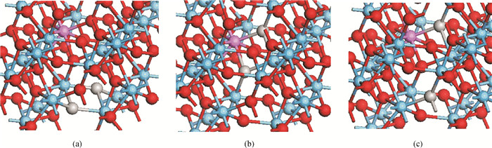
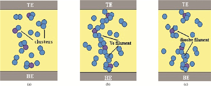
The physical mechanism of doping effects on switching uniformity and operation voltage in Al-doped HfO2 resistive random access memory (RRAM) devices is proposed from another perspective:defects interactions, based on first principle calculations. In doped HfO2, dopant is proved to have a localized effect on the formation of defects and the interactions between them. In addition, both effects cause oxygen vacancies (VO) to have a tendency to form clusters and these clusters are easy to form around the dopant. It is proved that this process can improve the performance of material through projected density of states (PDOS) analysis. For VO filament-type RRAM devices, these clusters are concluded to be helpful for the controllability of the switching process in which oxygen vacancy filaments form and break. Therefore, improved uniformity and operation voltage of Al-doped HfO2 RRAM devices is achieved.

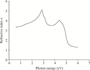
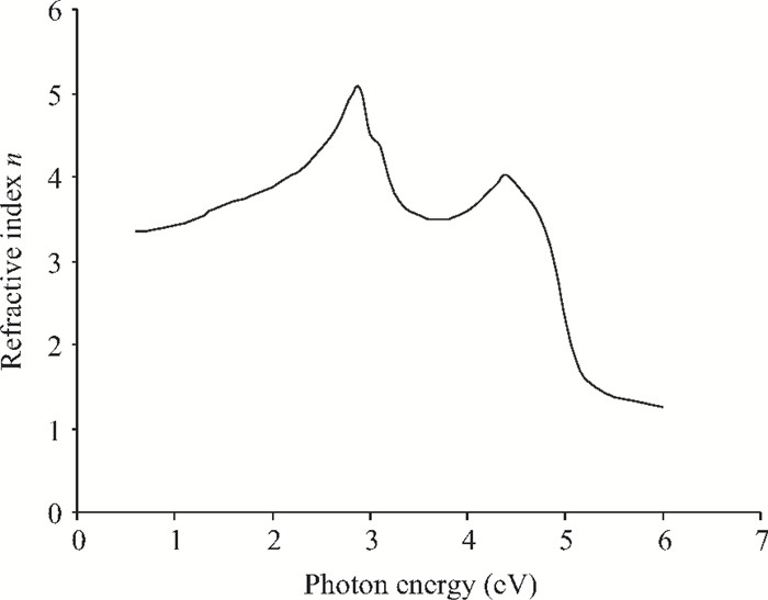
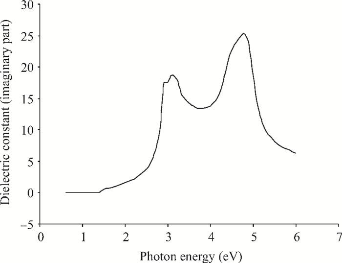
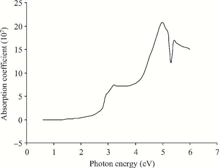
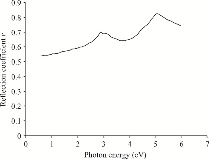
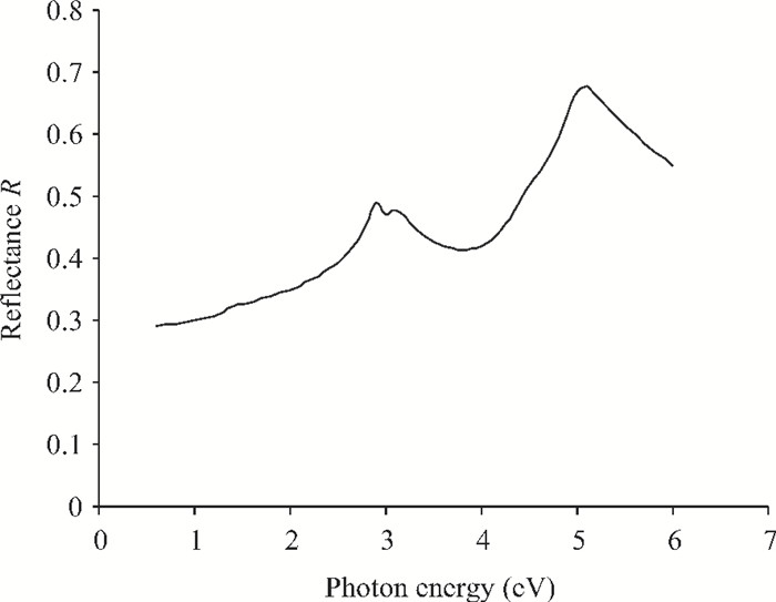
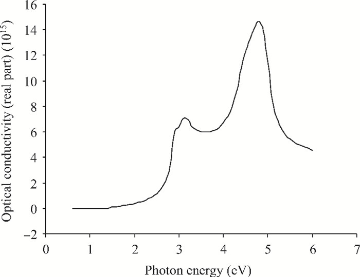
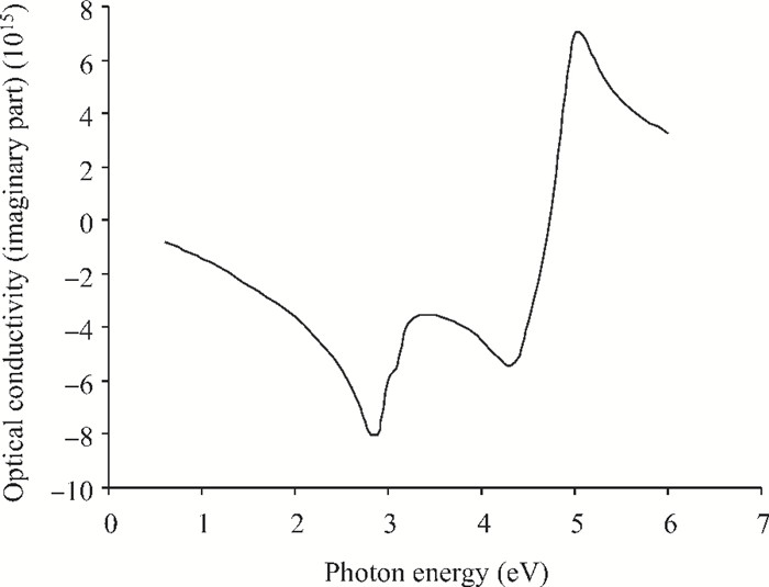
We have investigated the optical properties of gallium arsenide (GaAs) in the photon energy range 0.6-6.0 eV. We obtained a refractive index which has a maximum value of 5.0 at a photon energy of 3.1 eV; an extinction coefficient which has a maximum value of 4.2 at a photon energy of 5.0 eV; the dielectric constant, the real part of the complex dielectric constant has a maximum value of 24 at a photon energy of 2.8 eV and the imaginary part of the complex dielectric constant has a maximum value of 26.0 at a photon energy of 4.8 eV; the transmittance which has a maximum value of 0.22 at a photon energy of 4.0 eV; the absorption coefficient which has a maximum value of 0.22×10⁸ m-1 at a photon energy of 4.8 eV, the reflectance which has a maximum value of 0.68 at 5.2eV; the reflection coefficient which has a maximum value of 0.82 at a photon energy of 5.2 eV; the real part of optical conductivity has a maximum value of 14.2×10¹⁵ at 4.8 eV and the imaginary part of the optical conductivity has a maximum value of 6.8×10¹⁵ at 5.0 eV. The values obtained for the optical properties of GaAs are in good agreement with other results.


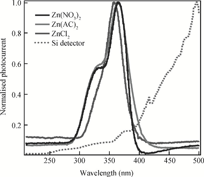
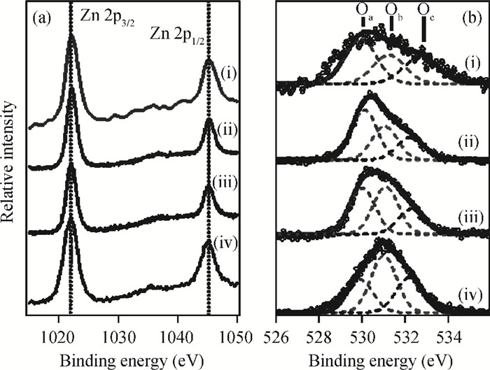
The fabrication of zinc oxide (ZnO) from inexpensive solution-processing techniques, namely, electrochemical deposition and electrospinning were explored on various conducting and mesoporous semiconducting surfaces. Optimised conditions were derived for template-and self-assisted nano/micro structures and composites. ZnO thin films were annealed at a fixed temperature under ambient conditions and characterised using physical and optical techniques. The photocurrent response in the UV region shows a fast rise and double decay behaviour with a fast component followed by a slow oscillatory decay. Photocurrent results were correlated with surface chemical analysis from X-ray photoelectron spectroscopy. Various characterisation details reveal the importance of fabrication parameter optimisation for useful low-cost optoelectronic applications.
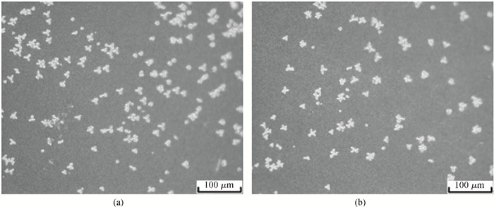
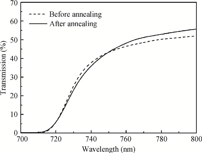
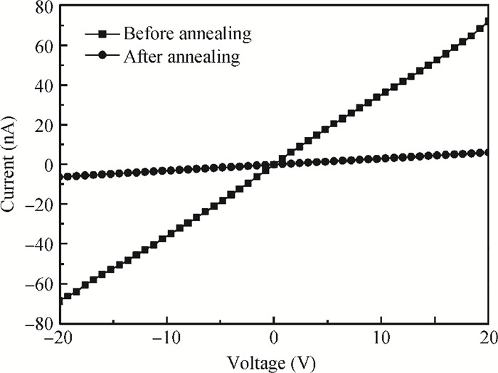
Thermal annealing in Te vapor atmosphere was adopted to improve the properties of indium-doped Cd1-xMnxTe (x=0.2, CdMnTe) wafers grown by the vertical Bridgman method. The wafers before and after annealing were characterized by measuring the Te inclusions, etch pit density (EPD), Mn composition, resistivity, and impurity. IR transmission microscopy and EPD measurements revealed that the densities of Te inclusions reduced from (5-9)×104 cm-3 to (2-4)×104 cm-3 and EPD from 105 cm-2 to 104 cm-2 after annealing. NIR transmission spectroscopy showed that the Mn composition increased by 0.002-0.005 mole fractions during the annealing. The resistivity of the wafers improved from (2.0-4.5)×108 Ω·cm to (1.7-3.8)×109 Ω·cm, which suggested that the deep-level donor of Te antisites was successfully introduced after annealing. Inductively coupled plasma-mass spectrometry (ICP-MS) revealed that the concentrations of impurities in the wafer decreased, which indicated the purifying effects of Te vapor annealing on the wafers. All the results demonstrate that the Te vapor annealing of the indium-doped CdMnTe crystal has positive effects on the crystallinity, resistivity and purity of CdMnTe wafers.

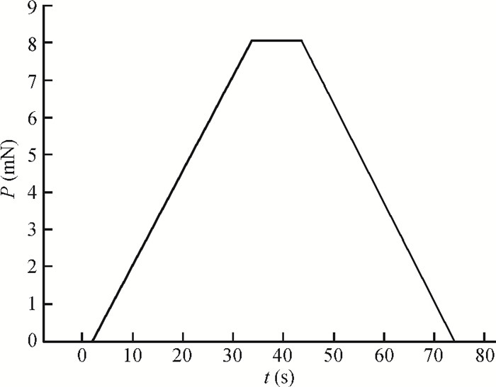
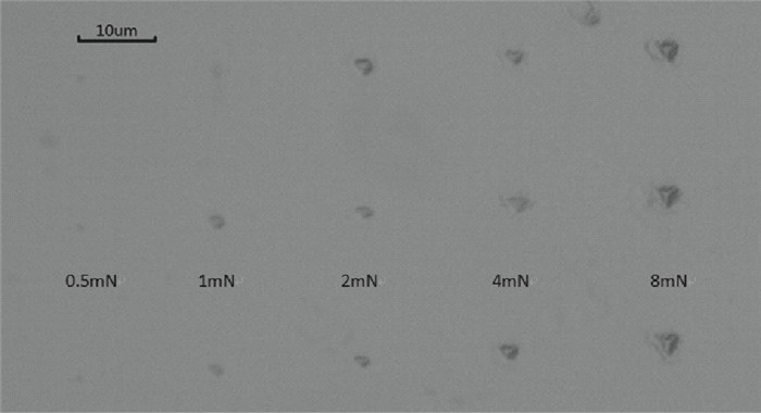
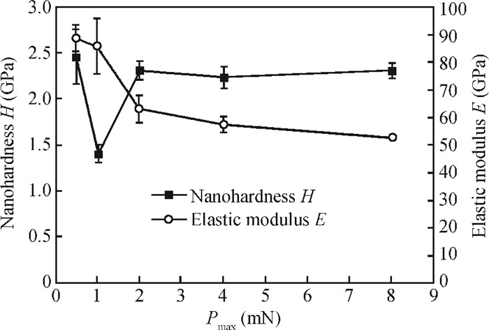
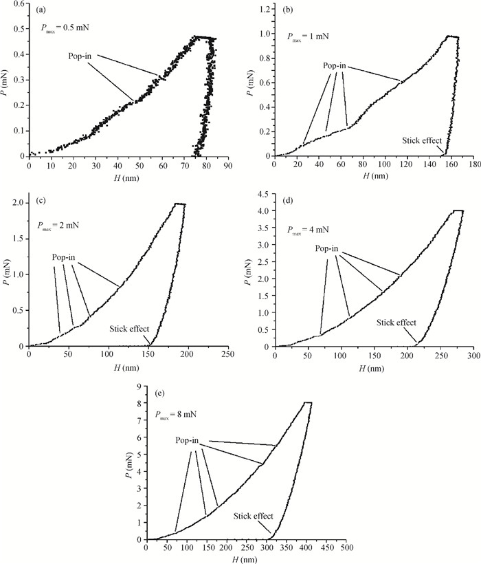
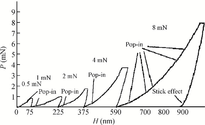
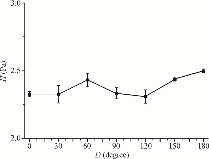
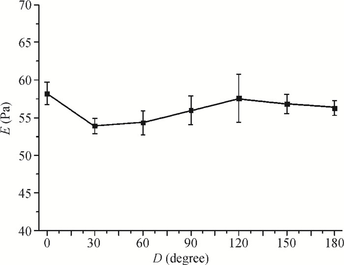
The nanohardness is from 1.44 to 2.61 GPa, the Vickers hardness is from 127 to 252 Vickers, and elastic modulus is from 52 to 123 GPa by the nanoindentation experiments on the doubler plane of KDP crystal. An indentation size effect is observed on the doubler plane in the test as the nanohardness and elastic modulus decreases with the increase of the maximum load. Slippage is identified as the major mode of plastic deformation, and pop-in events are attributed to the initiation of slippage. And the variation of unloading curve end is the result of stick effects between the indenter and the contact surface. The depth of the elastic deformation, which is between 40 and 75 nm, is responsible for the elastic deformation. The doubler plane of KDP crystal has anisotropy, and the relative anisotropy of nanohardness is 8.2% and the relative anisotropy of elastic modulus is 8.0%.

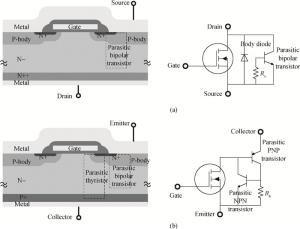
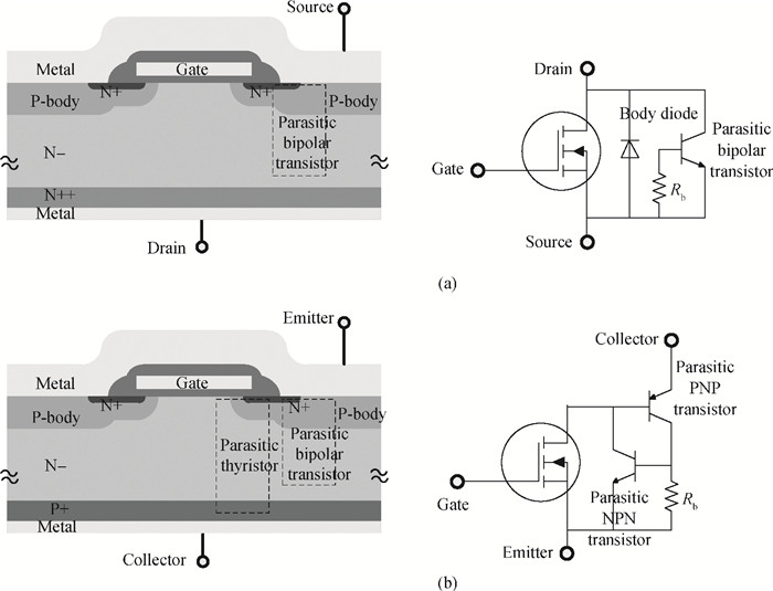
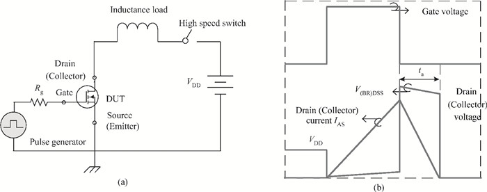
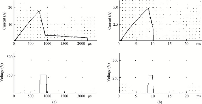
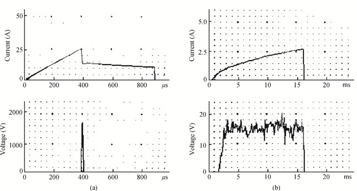
The ability of high-voltage power MOSFETs and IGBTs to withstand avalanche events under unclamped inductive switching (UIS) conditions is measured. This measurement is to investigate and compare the dynamic avalanche failure behavior of the power MOSFETs and the IGBT, which occur at different current conditions. The UIS measurement results at different current conditions show that the main failure reason of the power MOSFETs is related to the parasitic bipolar transistor, which leads to the deterioration of the avalanche reliability of power MOSFETs. However, the results of the IGBT show two different failure behaviors. At high current mode, the failure behavior is similar to the power MOSFETs situation. But at low current mode, the main failure mechanism is related to the parasitic thyristor activity during the occurrence of the avalanche process and which is in good agreement with the experiment result.
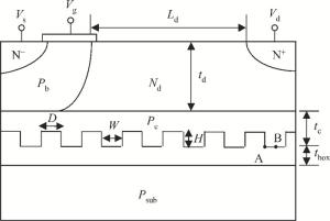
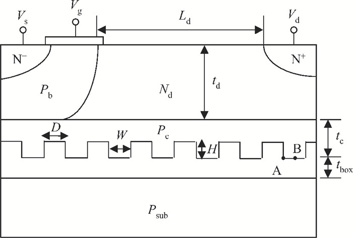
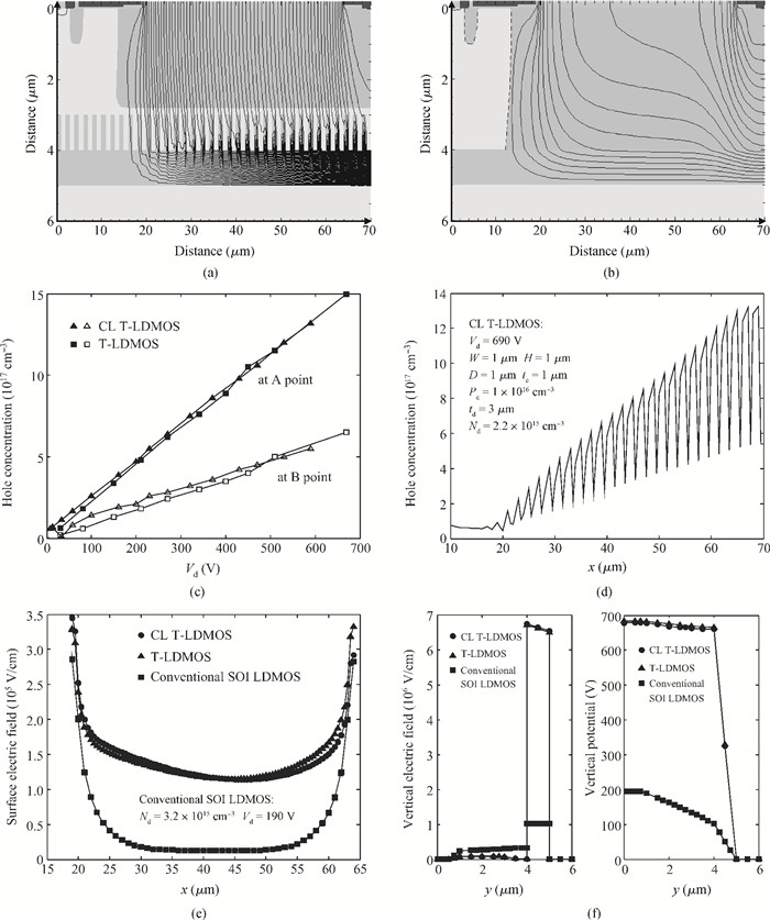
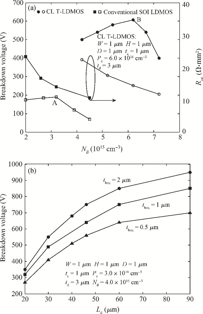
A new silicon-on-insulator (SOI) high-voltage MOSFET structure with a compensation layer on the trenched buried oxide layer (CL T-LDMOS) is proposed. The high density inverse interface charges at the top surface of the buried oxide layer (BOX) enhance the electric field in the BOX and a uniform surface electric field profile is obtained, which results in the enhancement of the breakdown voltage (BV). The compensation layer can provide additional P-type charges, and the optimal drift region concentration is increased in order to satisfy the reduced surface electric field (RESURF) condition. The numerical simulation results indicate that the vertical electric field in the BOX increases to 6 MV/cm and the BV of the proposed device increases by 300% in comparison to a conventional SOI LDMOS, while maintaining low on-resistance.

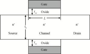
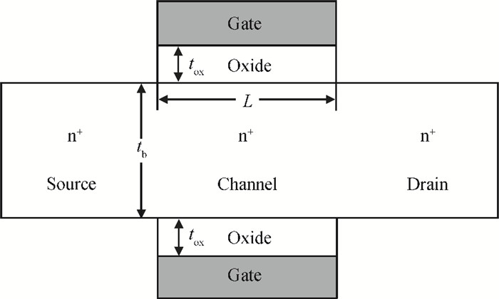
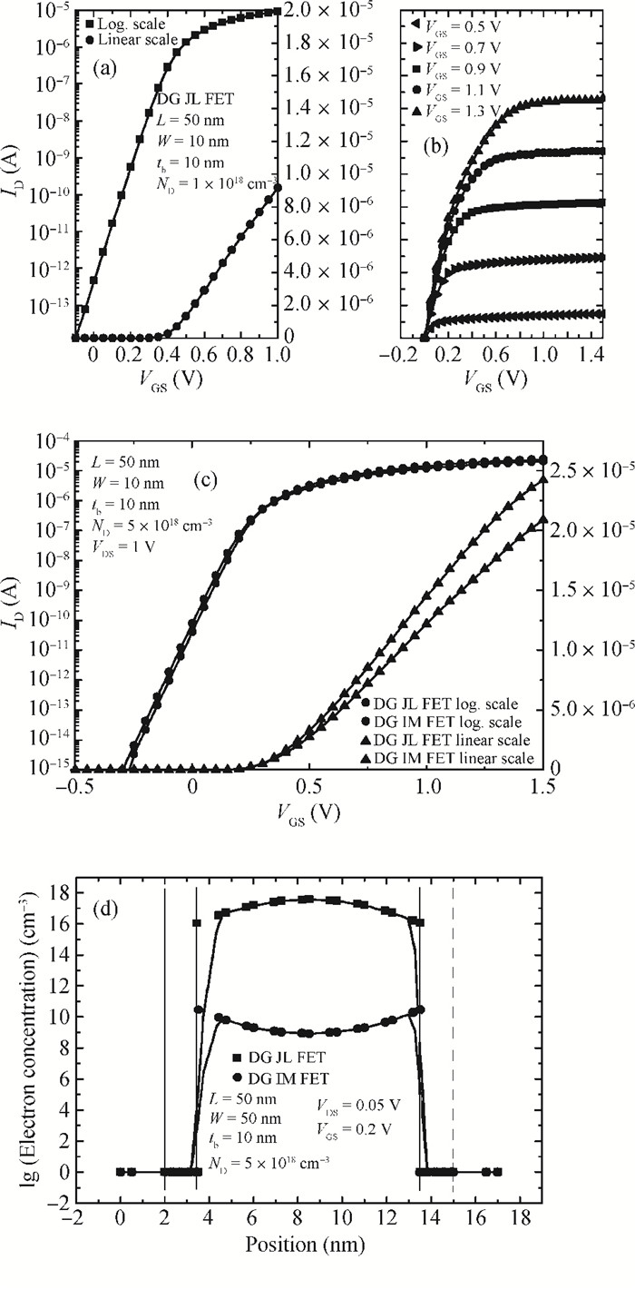
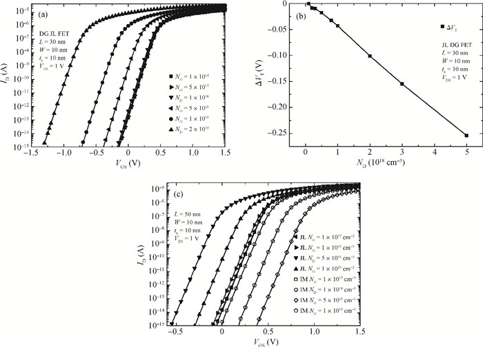
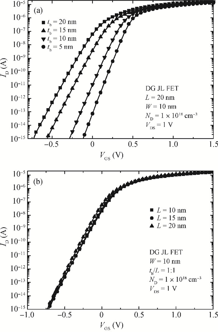
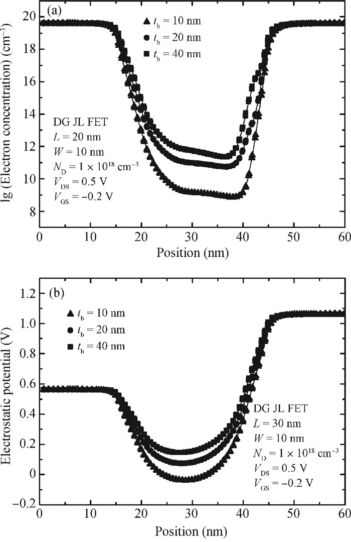
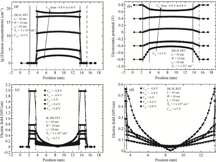
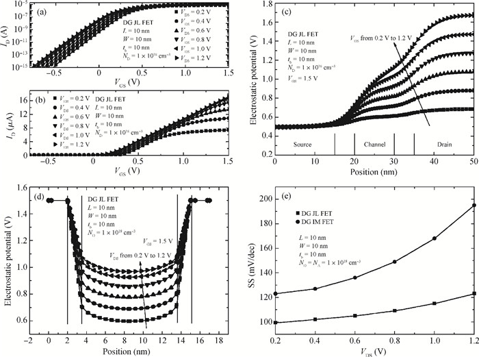
We study the characteristics of short channel double-gate (DG) junctionless (JL) FETs by device simulation. Output Ⅰ-Ⅴ characteristic degradations such as an extremely reduced channel length induced subthreshold slope increase and the threshold voltage shift due to variations of body doping and channel length have been systematically analyzed. Distributions of electron concentration, electric field and potential in the body channel region are also analyzed. Comparisons with conventional inversion-mode (IM) FETs, which can demonstrate the advantages of JL FETs, have also been performed.
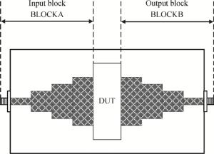
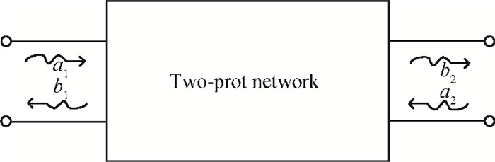
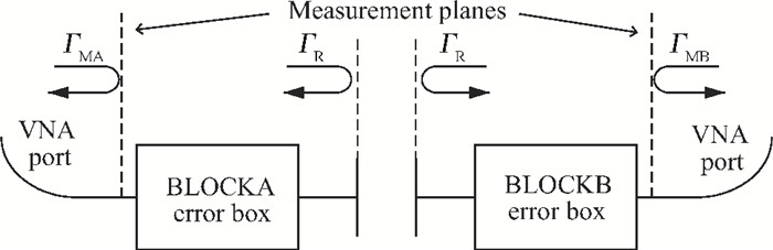
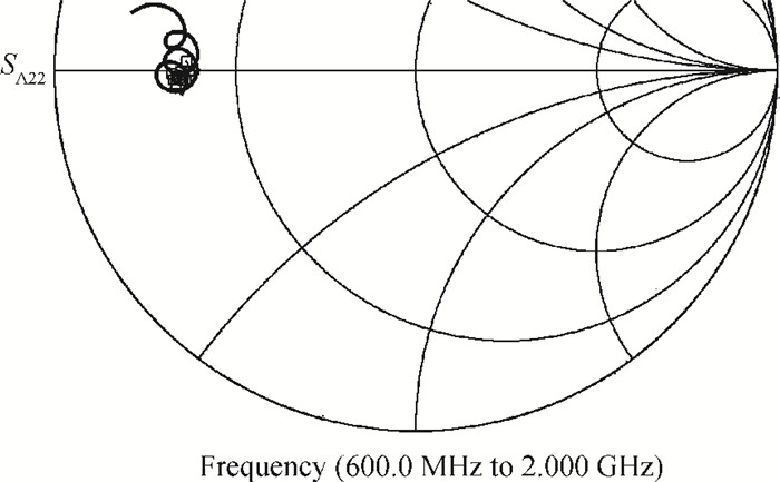
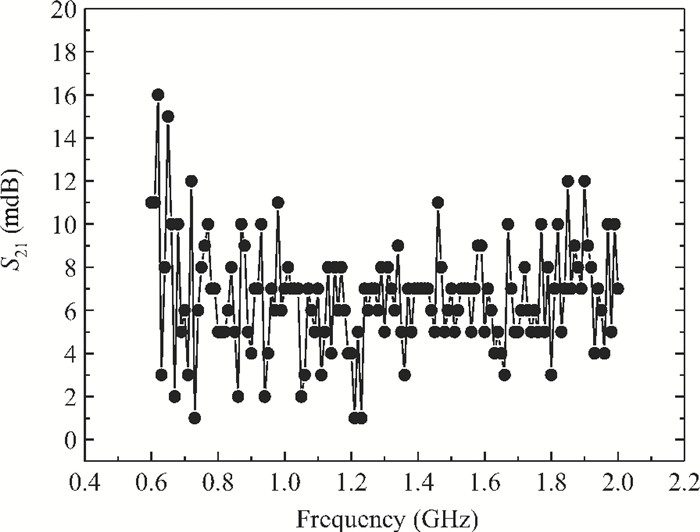
The impedance and output power measurements of LDMOS transistors are always a problem due to their low impedance and lead widths. An improved thru-reflect-line (TRL) calibration algorithm for measuring the characteristics of L-band high power LDMOS transistors is presented. According to the TRL algorithm, the individual two-port S parameters of each fixture half can be obtained. By de-embedding these S parameters of the test fixture, an accurate calibration can be made. The improved TRL calibration algorithm is successfully utilized to measure the characteristics of an L-band LDMOS transistor with a 90 mm gate width. The impedance of the transistor is obtained, and output power at 1 dB compression point can reach as much as 109.4 W at 1.2 GHz, achieving 1.2 W/mm power density. From the results, it is seen that the presented TRL calibration algorithm works well.


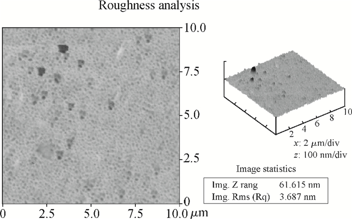
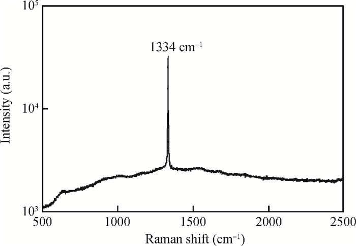
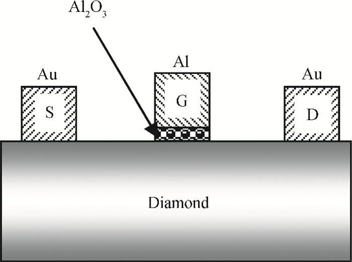
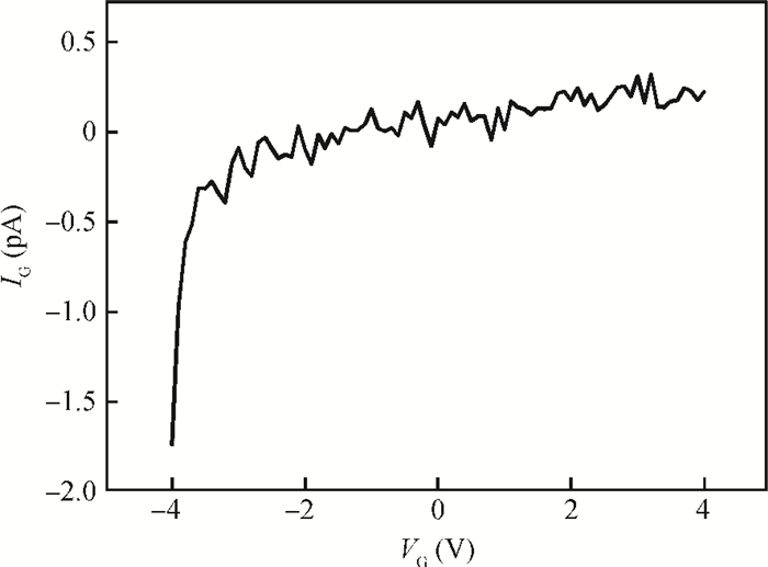
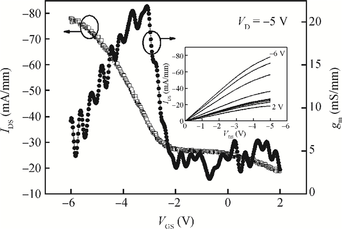
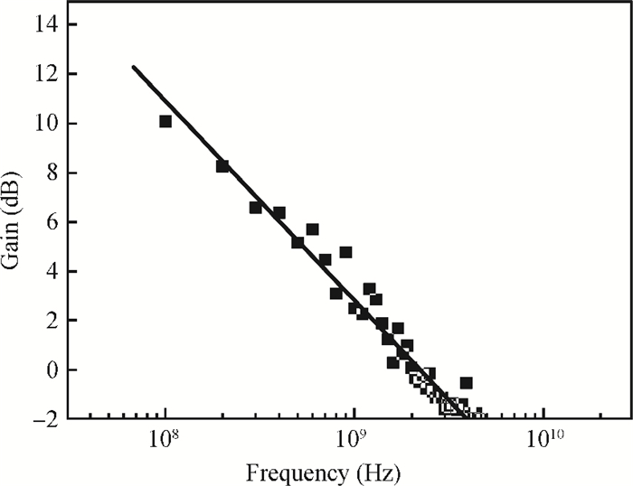
Based on the hydrogen-terminated surface channel diamond material, a 1 μm gate length diamond metal-insulator-semiconductor field-effect transistor (MISFET) was fabricated. The gate dielectric Al2O3 was formed by naturally oxidated thin Al metal layer, and a less than 2 pA gate leakage current was obtained at gate bias between -4 V and 4 V. The DC characteristic of the diamond MISFET showed a drain-current density of 80 mA/mm at drain voltage of -5 V, and a maximum transconductance of 22 mS/mm at gate-source voltage of -3 V. With the small signal measurement, a current gain cutoff frequency of 2.1 GHz was also obtained.
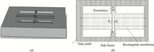
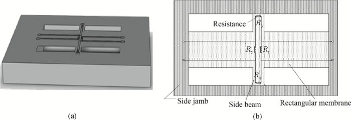
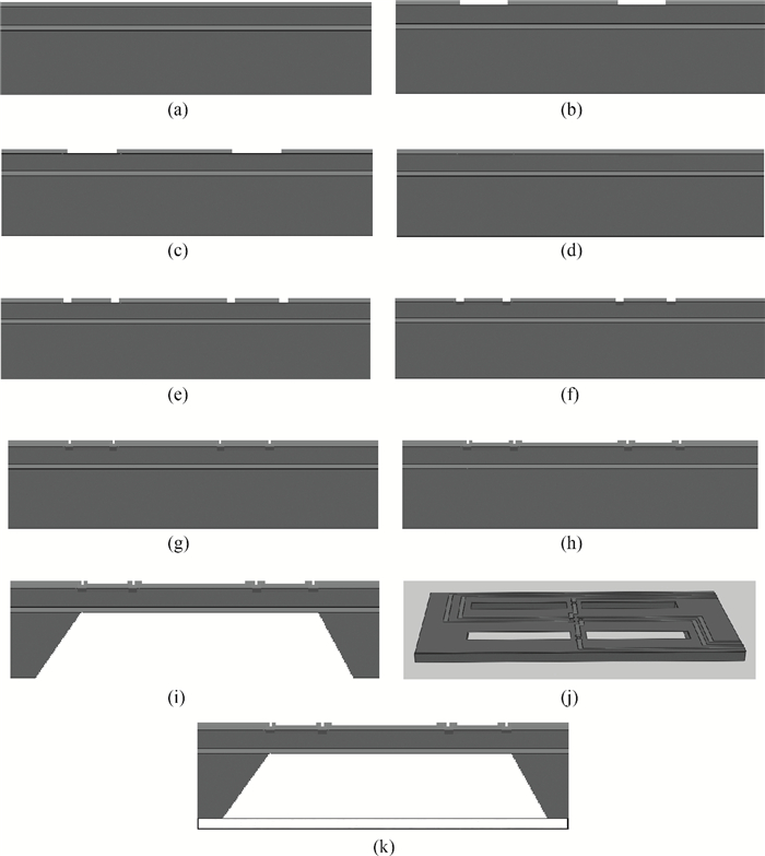
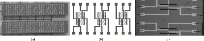
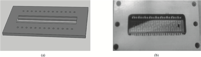
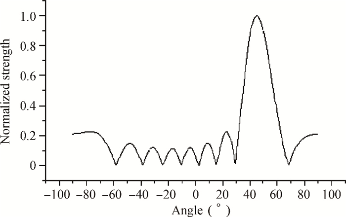
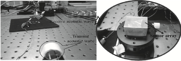
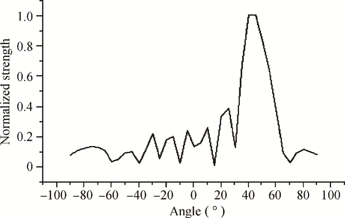
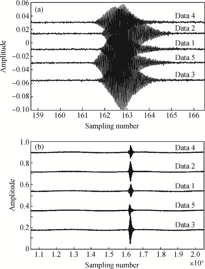
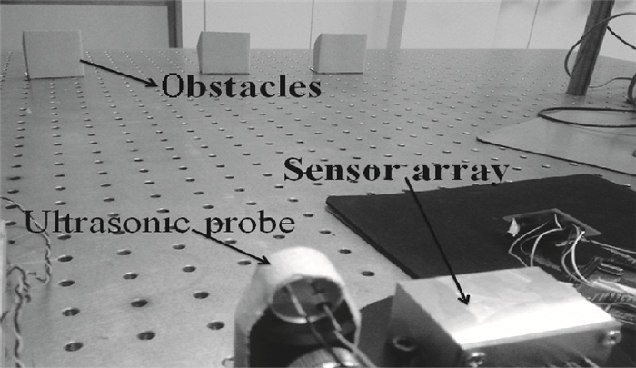
The design, fabrication and packaging of a type of MEMS piezoresistive ultrasonic transducer array are introduced. The consistency of the resonance frequency and the sensitivity of the array are tested. Moreover, we detect the directivity and the multi-target identification ability of the array. The results of the consistency of the resonance frequency and the sensitivity show that there is a gap between the practical and theoretical results. This paper analyzes this problem in detail and points out the direction of improvement. As for the directivity, the actual result is consistent with the theoretical one. The results of multiple target distinguishing tests demonstrate that the smallest resolution angle of the array is 5.72° when the distance between the sensor array and measured objects is 2 m.
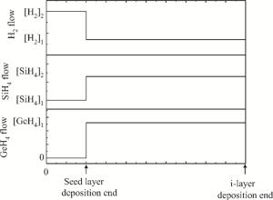
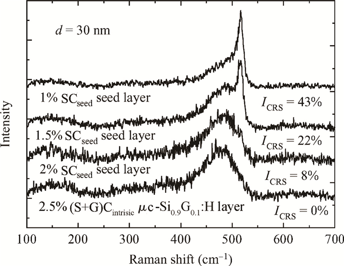
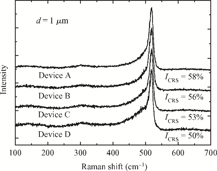
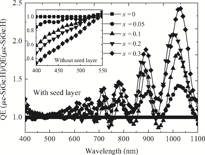
Using plasma enhanced chemical vapor deposition (PECVD) at 13.56 MHz, a seed layer is fabricated at the initial growth stage of the hydrogenated microcrystalline silicon germanium (μc-Si1-xGex:H) i-layer. The effects of seeding processes on the growth of μc-Si1-xGex:H i-layers and the performance of μc-Si1-xGex:H p-i-n single junction solar cells are investigated. By applying this seeding method, the μc-Si1-xGex:H solar cell shows a significant improvement in short circuit current density (Jsc) and fill factor (FF) with an acceptable performance of blue response as a μc-Si:H solar cell even when the Ge content x increases up to 0.3. Finally, an improved efficiency of 7.05% is achieved for the μc-Si0.7Ge0.3:H solar cell.


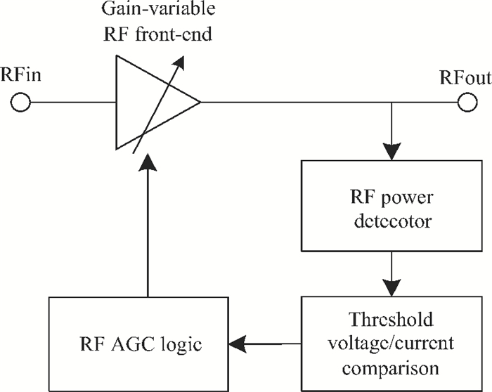
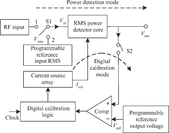
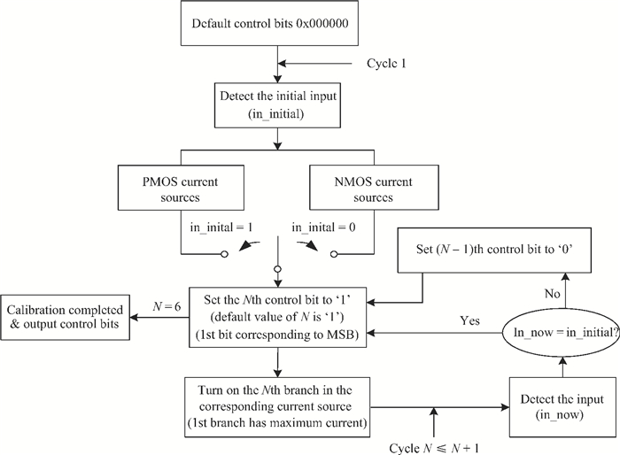
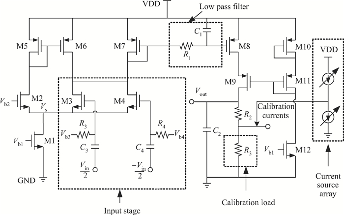
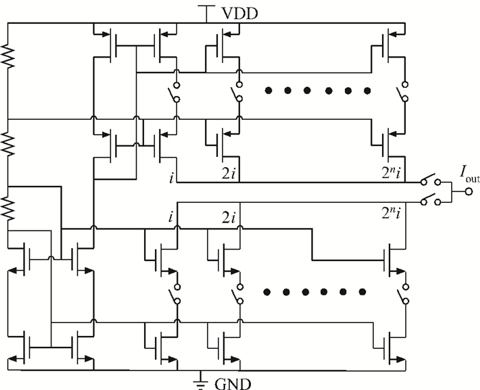
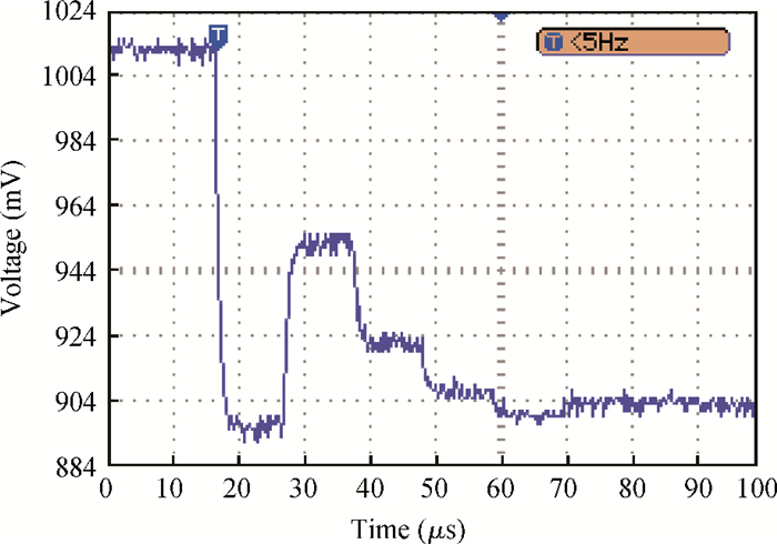
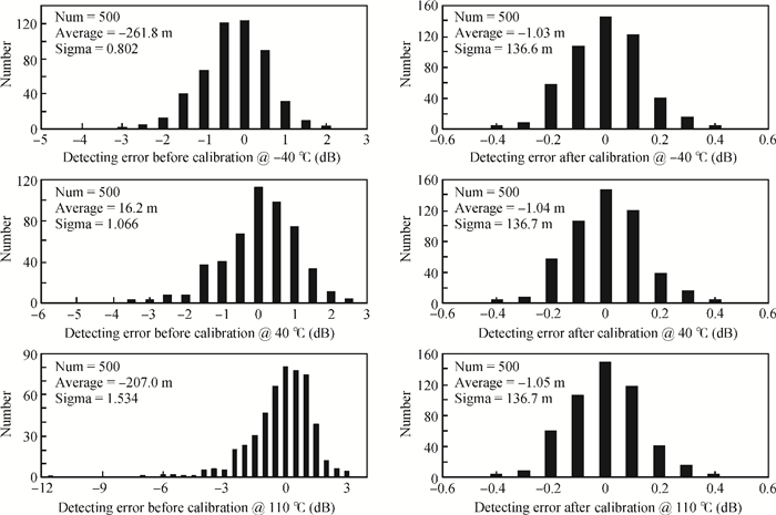
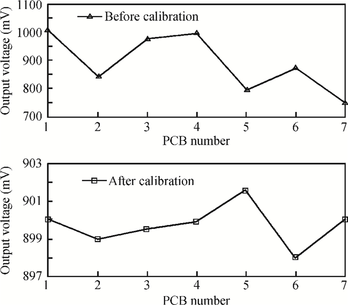
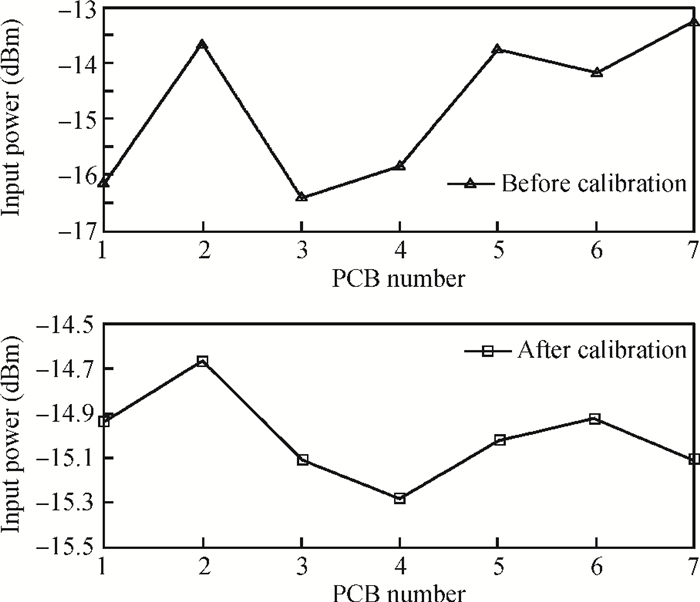
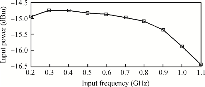
This paper presents the design and implementation of a digitally calibrated CMOS wideband radio frequency (RF) root-mean-square (RMS) power detector for high accuracy RF automatic gain control (AGC). The proposed RMS power detector demonstrates accurate power detection in the presence of process, supply voltage, and temperature (PVT) variations by employing a digital calibration scheme. It also consumes low power and occupies a small chip area. The measurement results show that the scheme improves the accuracy of the detector to better than 0.3 dB over the PVT variations and wide operating frequency range from 0.2 to 0.8 GHz. Implemented in a 0.18 μm CMOS process and occupying a small die area of 263×214 μm2, the proposed digitally calibrated CMOS RMS power detector only consumes 1.6 mA in power detection mode and 2.1 mA in digital calibration mode from a 1.8 V supply voltage.


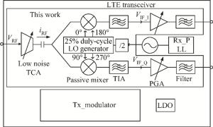
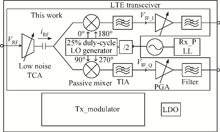
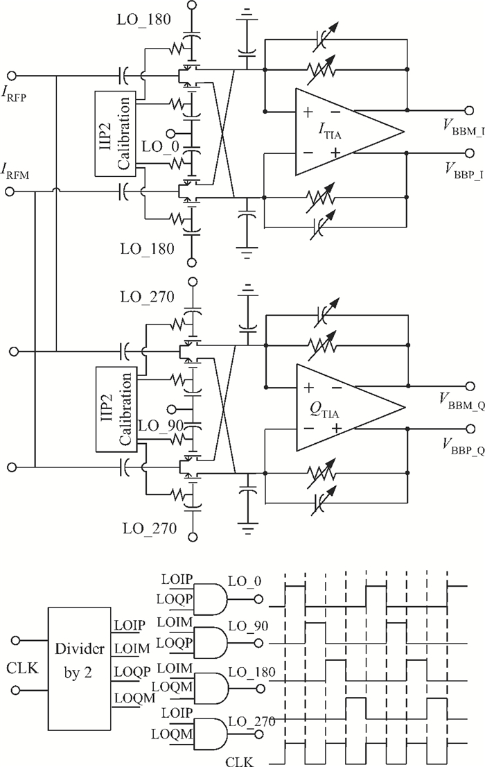
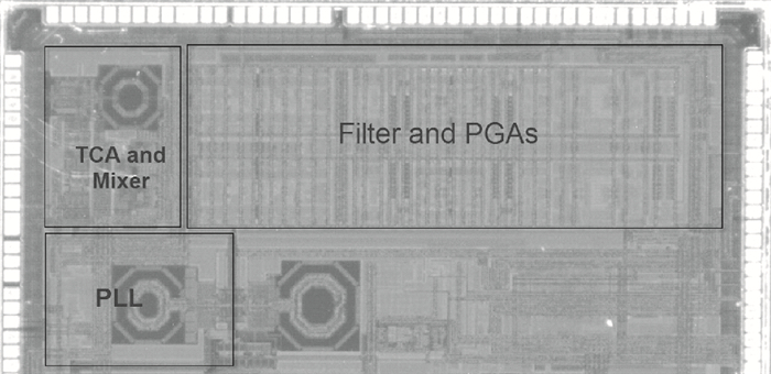
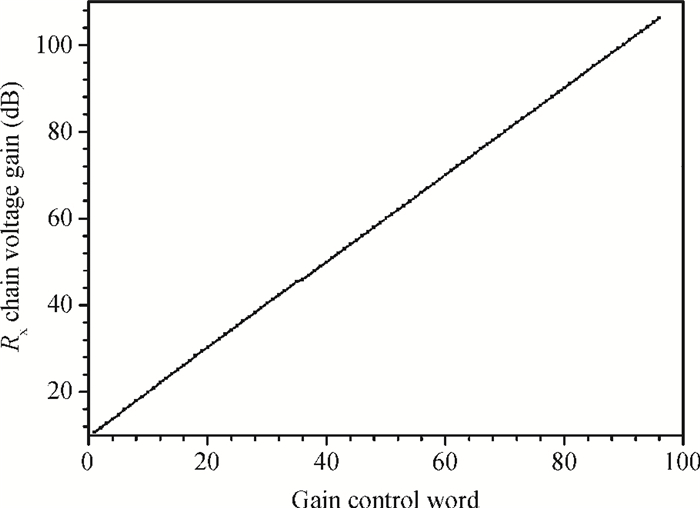
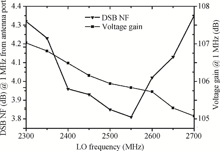
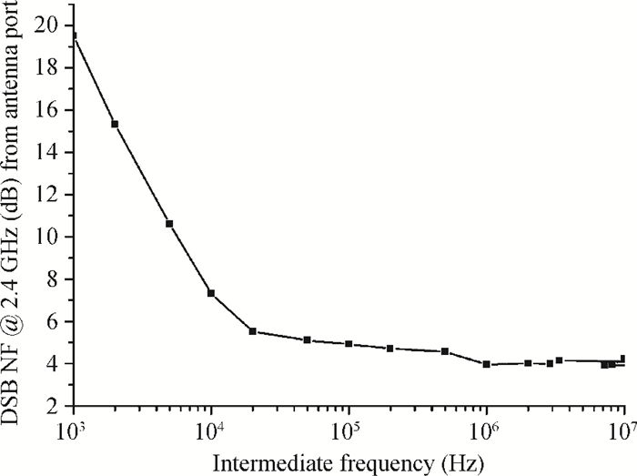
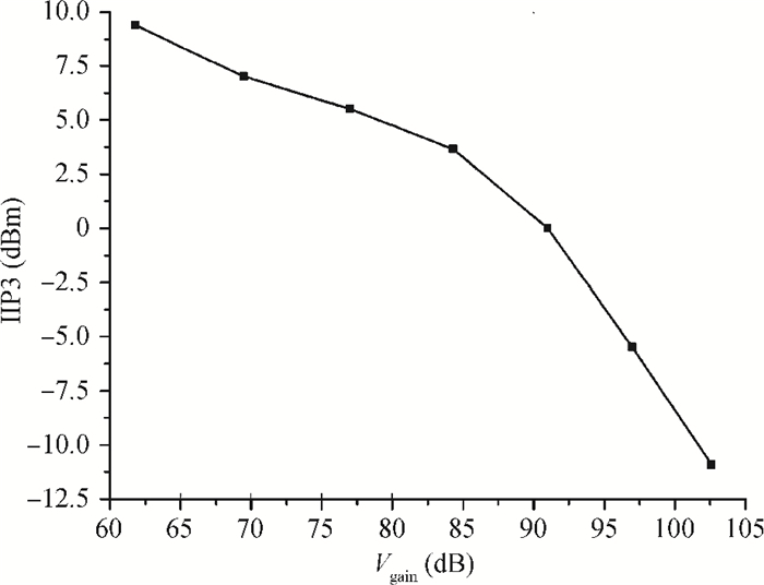
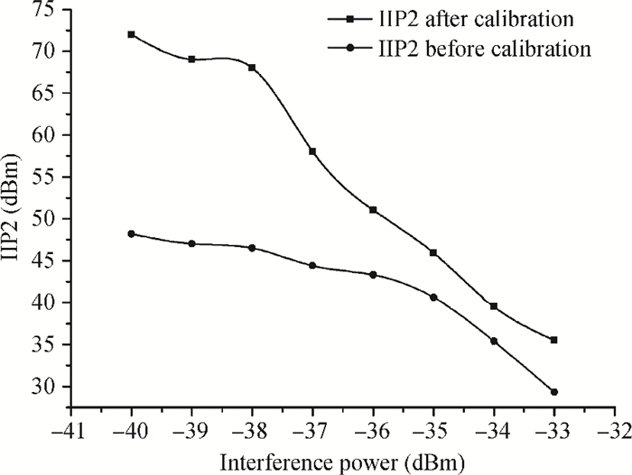
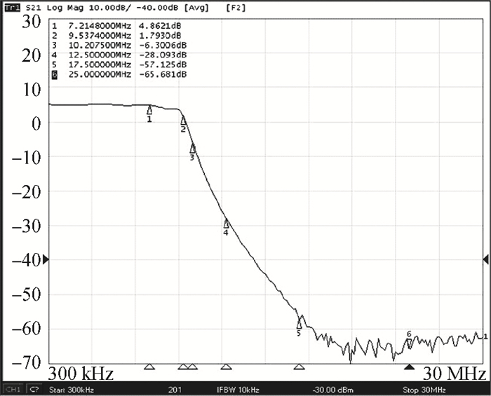
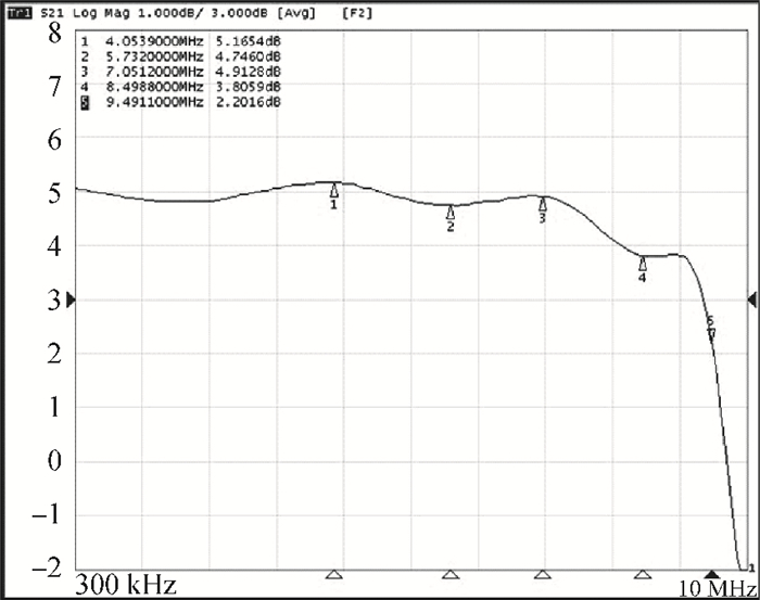
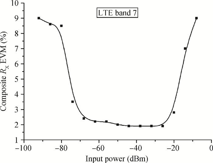
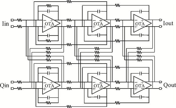
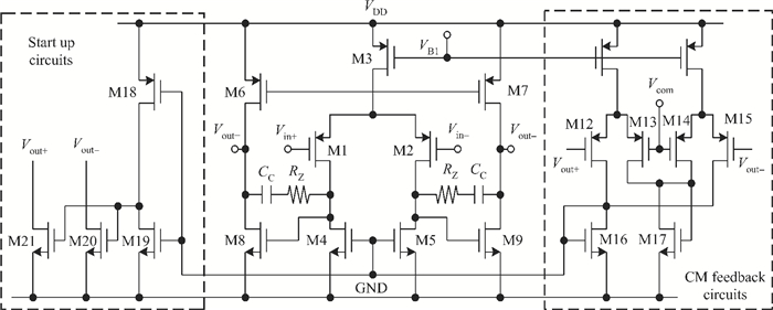
A CMOS long-term evolution (LTE) direct convert receiver that eliminates the interstage SAW filter is presented. The receiver consists of a low noise variable gain transconductance amplifier (TCA), a quadrature passive current commutating mixer with a 25% duty-cycle LO, a trans-impedance amplifier (TIA), a 7th-order Chebyshev filter and programmable gain amplifiers (PGAs). A wide dynamic gain range is allocated in the RF and analog parts. A current commutating passive mixer with a 25% duty-cycle LO improves gain, noise, and linearity. An LPF based on a Tow-Thomas biquad suppresses out-of-band interference. Fabricated in a 0.13 μm CMOS process, the receiver chain achieves a 107 dB maximum voltage gain, 2.7 dB DSB NF (from PAD port), -11 dBm ⅡP3, and > +65 dBm ⅡP2 after calibration, 96 dB dynamic control range with 1 dB steps, less than 2% error vector magnitude (EVM) from 2.3 to 2.7 GHz. The total receiver (total I Q path) draws 89 mA from a 1.2-V LDO on chip supply.

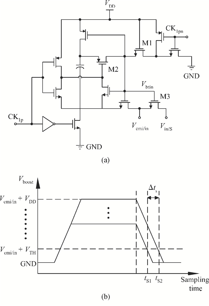
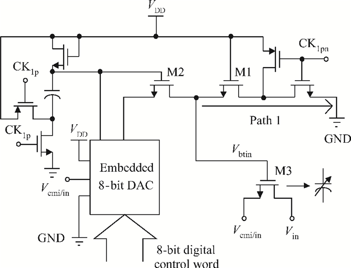
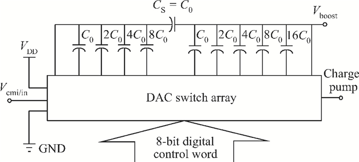
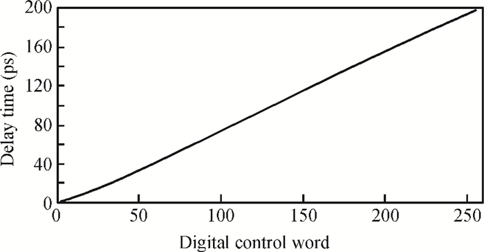
A sampling switch with an embedded digital-to-skew converter (DSC) is presented. The proposed switch eliminates time-interleaved ADCs' skews by adjusting the boosted voltage. A similar bridged capacitors' charge sharing structure is used to minimize the area. The circuit is fabricated in a 0.18 μm CMOS process and achieves sub-1 ps resolution and 200 ps timing range at a rate of 100 MS/s. The power consumption is 430 μW at maximum. The measurement result also includes a 2-channel 14-bit 100 MS/s time-interleaved ADCs (TI-ADCs) with the proposed DSC switch's demonstration. This scheme is widely applicable for the clock skew and aperture error calibration demanded in TI-ADCs and SHA-less ADCs.
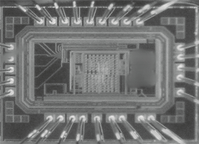

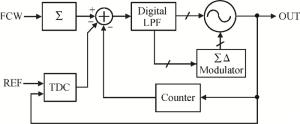
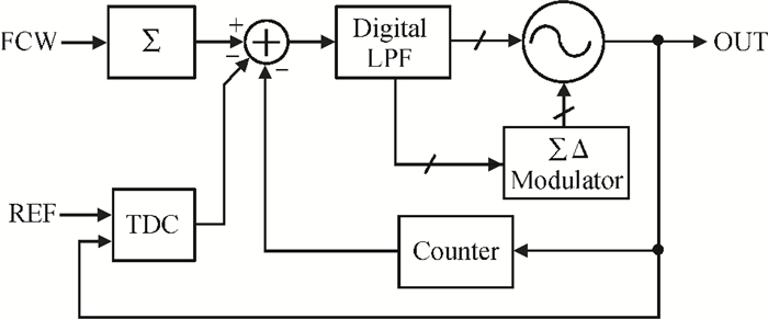
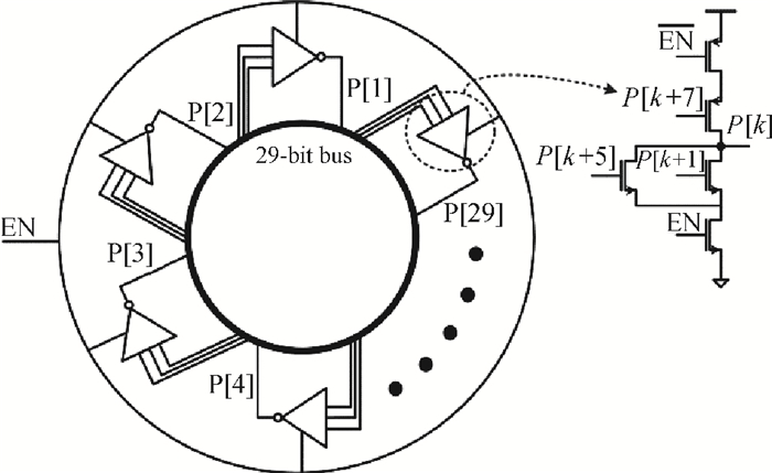
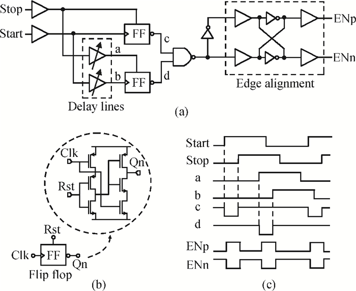
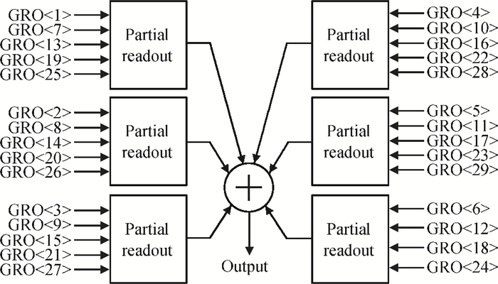
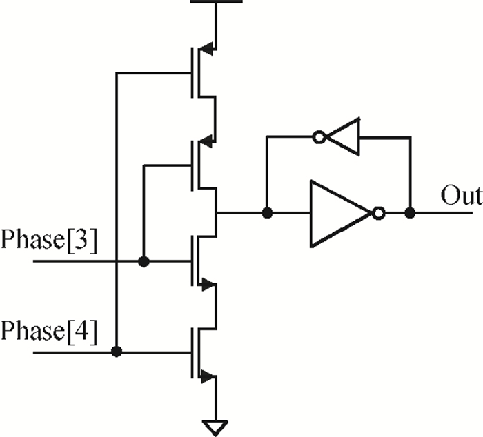
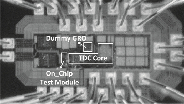
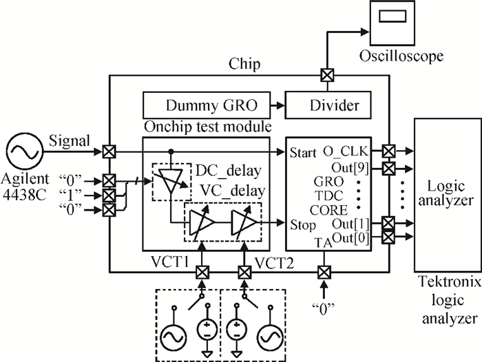
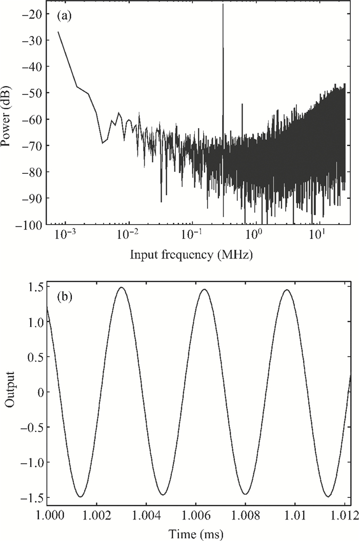
A gated ring oscillator (GRO) based time-to-digital converter (TDC) is presented. To enhance the resolution of the TDC, a multi-path structure for the GRO is used to achieve a higher oscillation frequency and an input stage is also presented to equivalently amplify the input time difference with a gain of 2. The GRO based TDC circuit is fabricated in TSMC 65 nm CMOS technology and the core area is about 0.02 mm2. According to the measurement results, the effective resolution of this circuit is better than 4.22 ps under a 50 MHz clock frequency. With a 1 ns input range, the maximum clock frequency of this circuit is larger than 200 MHz. Under a 1 V power supply, with a 200-800 ps input time difference, the measured power consumption is 1.24 to 1.72 mW at 50 MHz clock frequency and 1.73 to 2.20 mW at 200 MHz clock frequency.


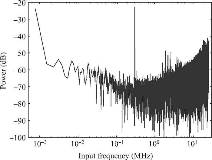
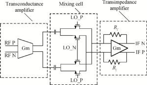
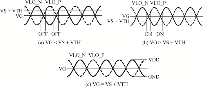
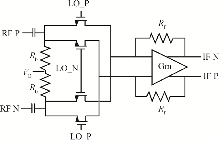
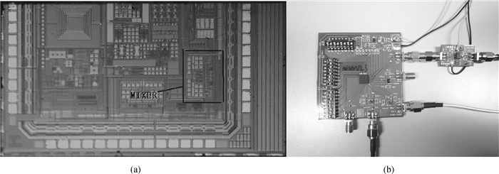
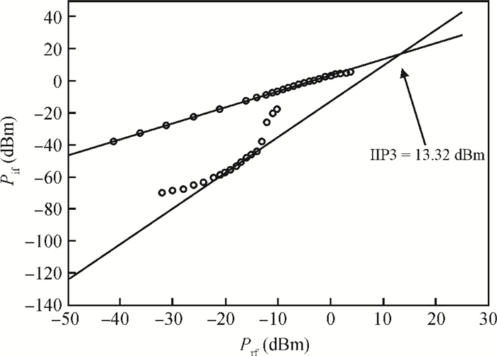
A high linearity current communicating passive mixer including the mixing cell and transimpedance amplifier (TIA) is introduced. It employs the resistor in the TIA to reduce the source voltage and the gate voltage of the mixing cell. The optimum linearity and the maximum symmetric switching operation are obtained at the same time. The mixer is implemented in a 0.25 μm CMOS process. The test shows that it achieves an input third-order intercept point of 13.32 dBm, conversion gain of 5.52 dB, and a single sideband noise figure of 20 dB.
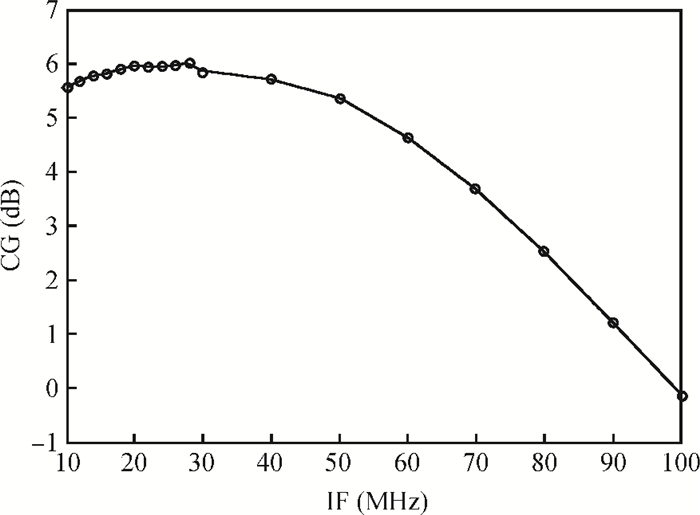
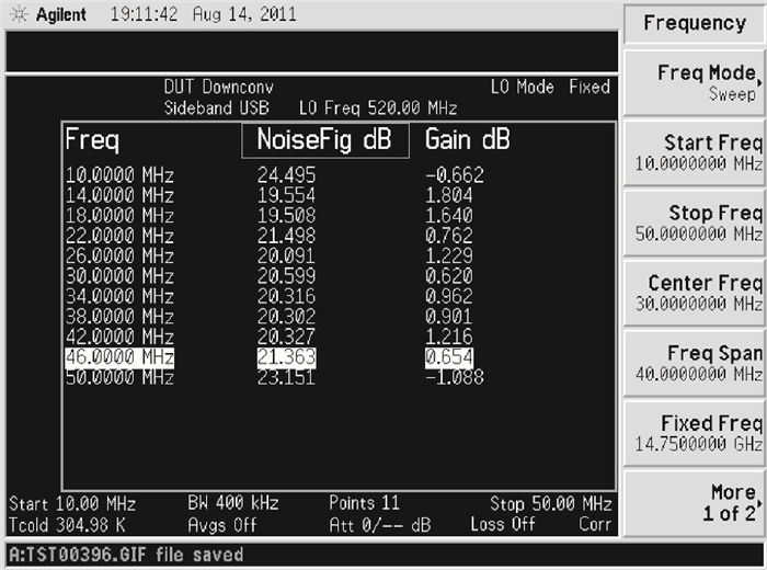
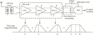
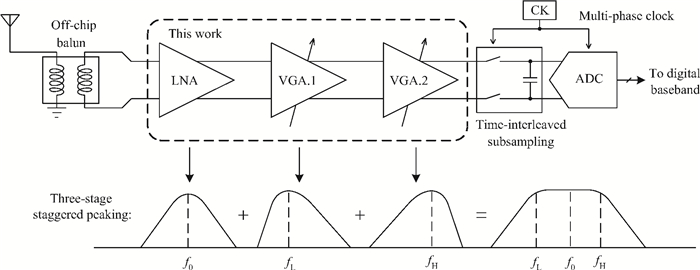
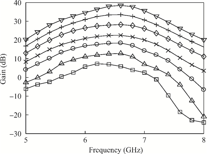
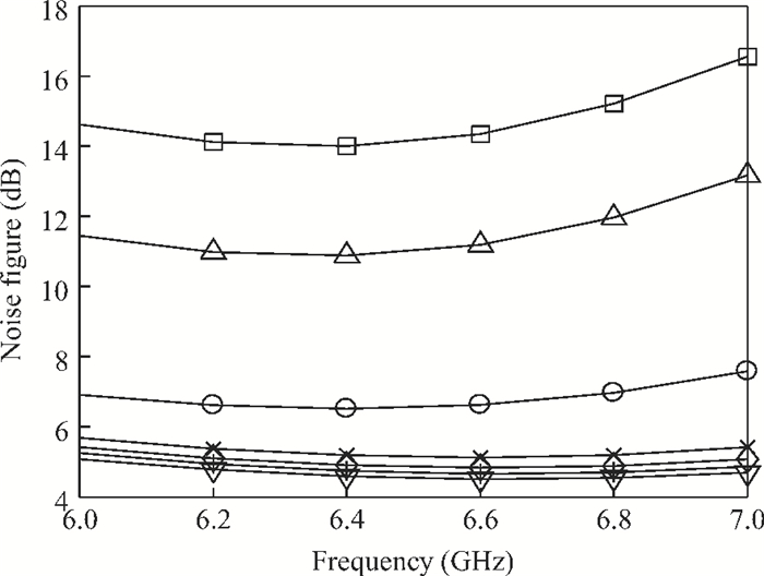
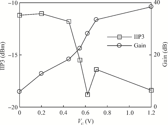
A wideband receiver RF front-end for IR-UWB applications is implemented in 0.13 μm CMOS technology. Thanks to the direct sub-sampling architecture, there is no mixing process. Both LNA and VGA work at RF frequencies. To optimize noise as well as linearity, a differential common-source LNA with capacitive cross-coupling is used, which only consumes current of 1.8 mA from a 1.2 V power supply. Following LNA, a two-stage current-steering VGA is adopted for gain tuning. To extend the overall bandwidth, a three-stage staggered peaking technique is used. Measurement results show that the proposed receiver front-end achieves a gain tuning range from 5 to 40 dB within 6-7 GHz, a minimum noise figure of 4.5 dB and a largest ⅡP3 of -11 dBm. The core receiver (without test buffer) consumes 14 mW from a 1.2 V power supply and occupies 0.58 mm2 area.

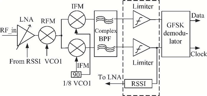
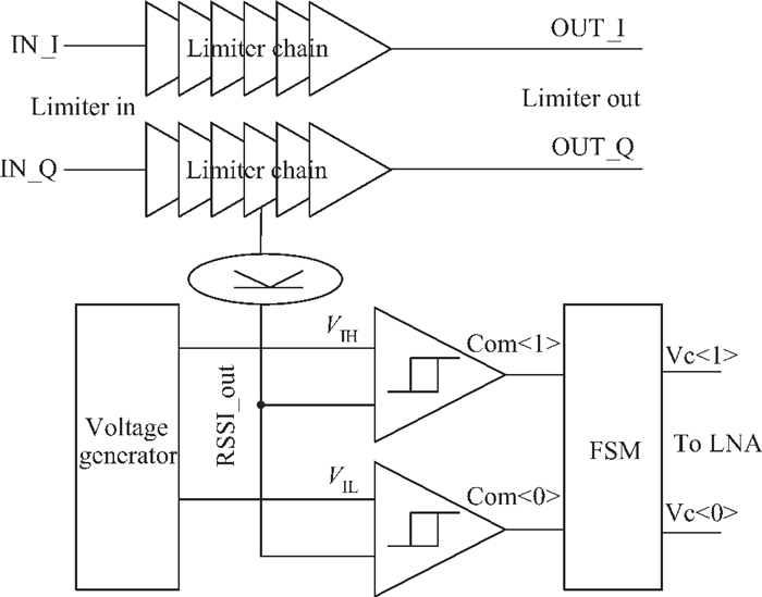
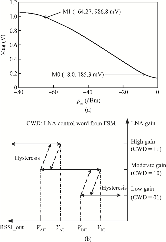
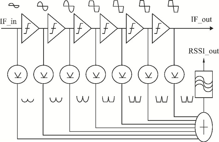
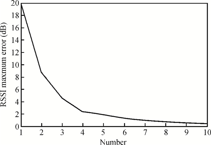
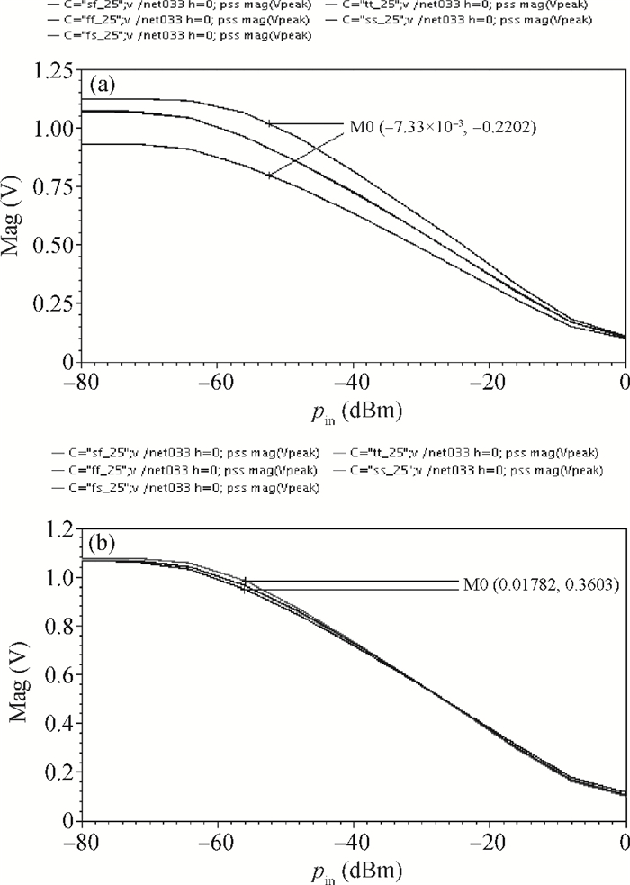
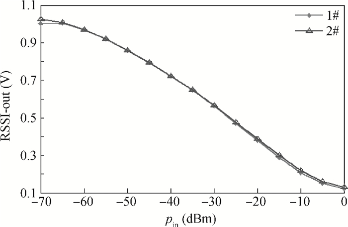
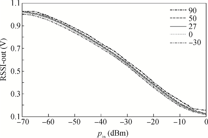
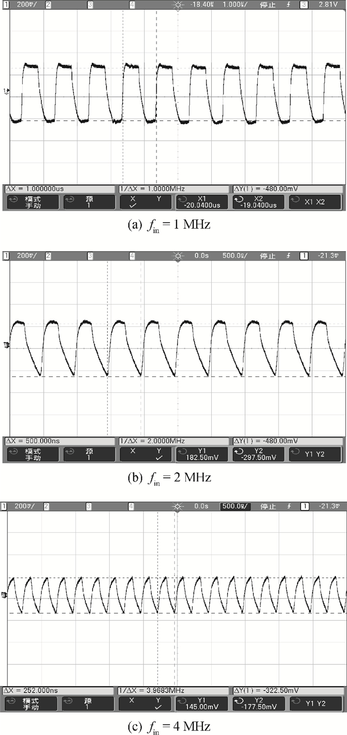
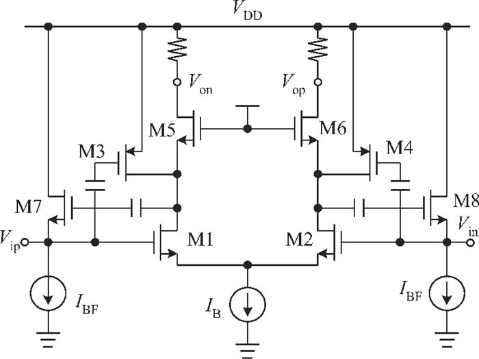
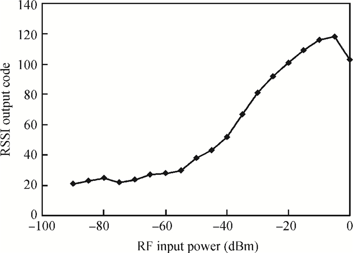
A low voltage low power CMOS limiter and received signal strength indicator (RSSI) with an integrated automatic gain control (AGC) loop for a short-distance receiver are implemented in SMIC 0.13 μm CMOS technology. The RSSI has a dynamic range of more than 60 dB and the RSSI linearity error is within ±0.5 dB for an input power from -65 to -8 dBm. The RSSI output voltage is from 0.15 to 1 V and the slope of the curve is 14.17 mV/dB while consuming 1.5 mA (I and Q paths) from a 1.2 V supply. Auto LNA gain mode selection with a combined RSSI function is also presented. Furthermore, with the compensation circuit, the proposed RSSI shows good temperature-independent and good robustness against process variation characteristics.


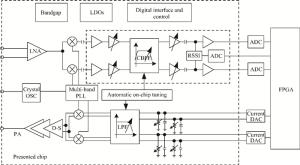
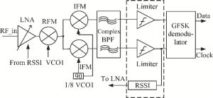
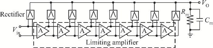
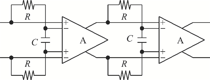
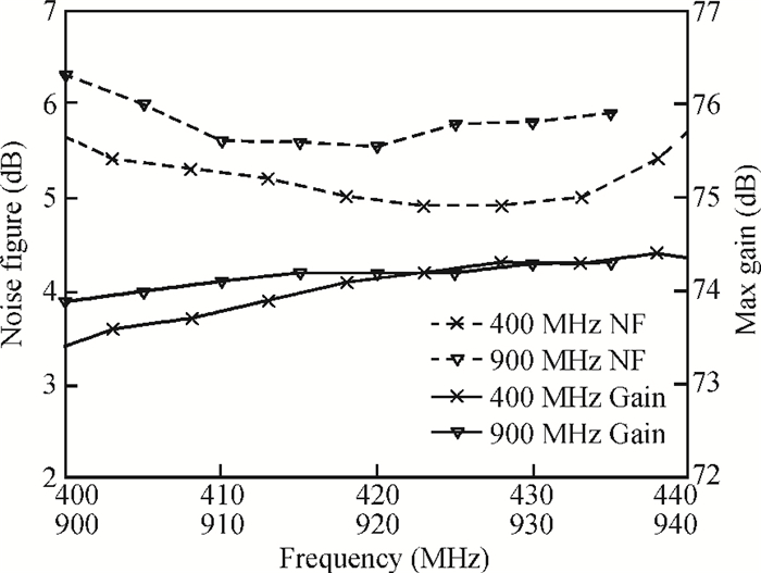
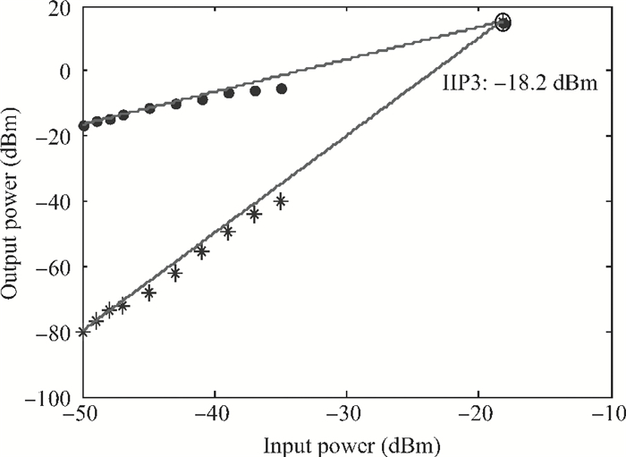
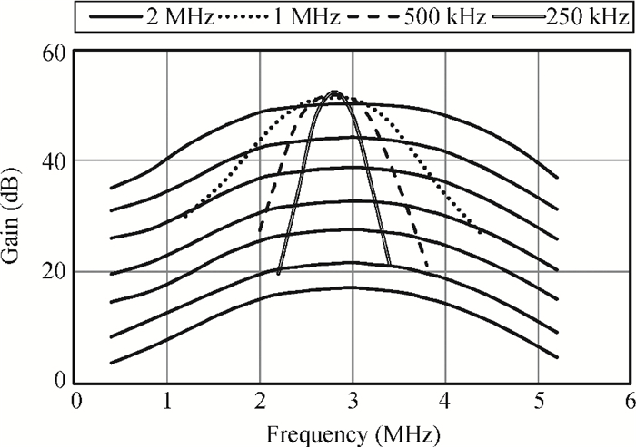
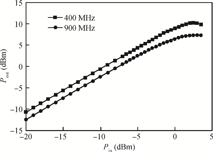
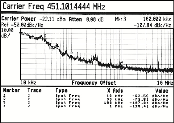
A reconfigurable multi-mode multi-band transceiver for low power short-range wireless communication applications is presented. Its low intermediate frequency (IF) receiver with 3 MHz IF carrier frequency and the direct-conversion transmitter support reconfigurable signal bandwidths from 250 kHz to 2 MHz and support a highest data rate of 3 Mbps for MSK modulation. An integrated multi-band PLL frequency synthesizer is utilized to provide the quadrature LO signals from about 300 MHz to 1 GHz for the transceiver multi-band application. The transceiver has been implemented in a 0.18 μm CMOS process. The measurement results at the maximum gain mode show that the receiver achieves a noise figure (NF) of 4.9/5.5 dB and an input 3rd order intermodulation point (ⅡP3) of -19.6/-18.2 dBm in 400/900 MHz band. The transmitter working in 400/900 MHz band can deliver 10.2/7.3 dBm power to a 50 Ω load. The transceiver consumes 32.9/35.6 mW in receive mode and 47.4/50.1 mW in transmit mode in 400/900 MHz band, respectively.


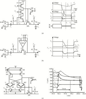
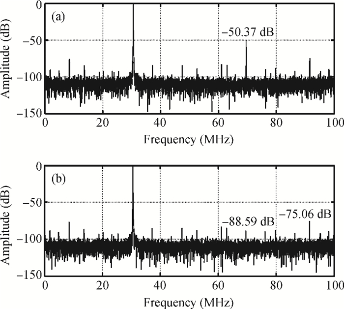
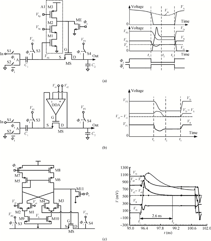
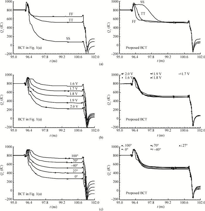
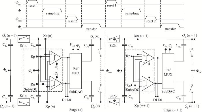
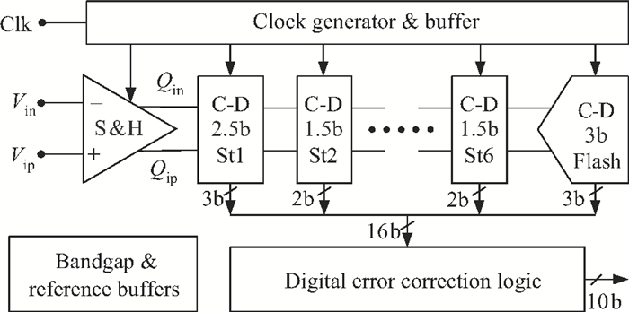
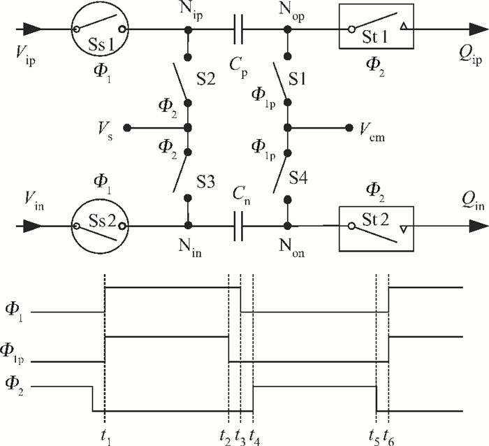
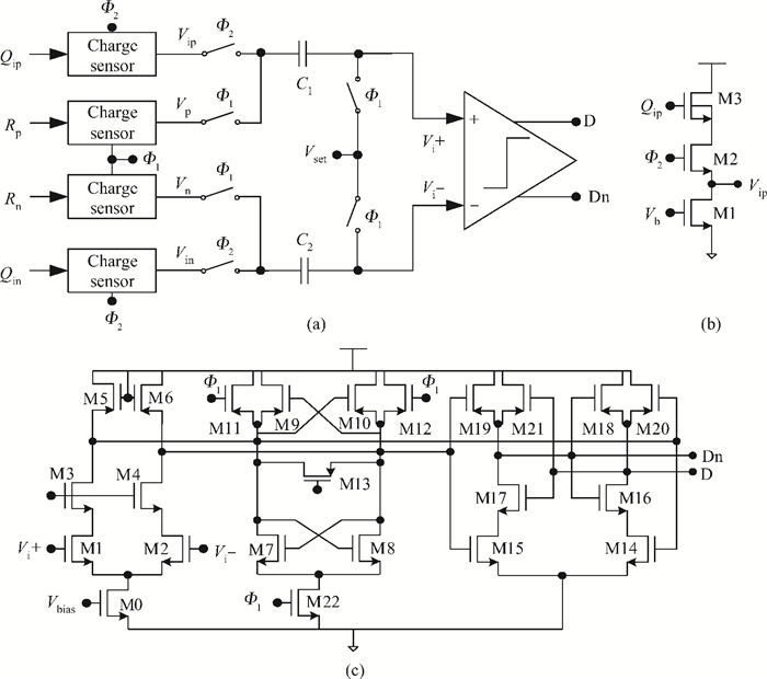
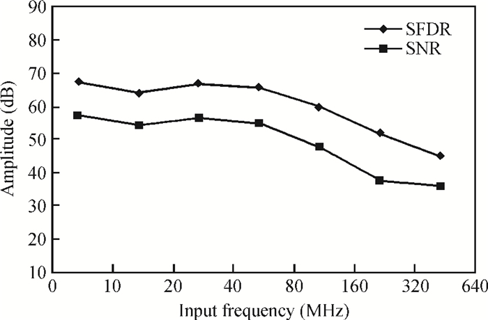
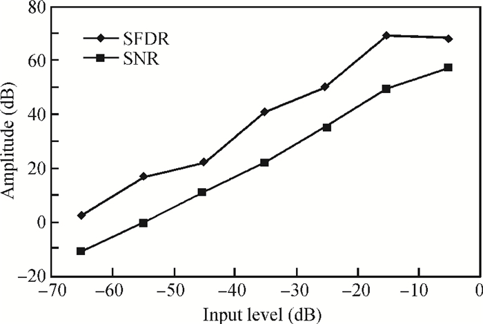
A low power 10-bit 125-MSPS charge-domain (CD) pipelined analog-to-digital converter (ADC) based on MOS bucket-brigade devices (BBDs) is presented. A PVT insensitive boosted charge transfer (BCT) that is able to reject the charge error induced by PVT variations is proposed. With the proposed BCT, the common mode charge control circuit can be eliminated in the CD pipelined ADC and the system complexity is reduced remarkably. The prototype ADC based on the proposed BCT is realized in a 0.18 μm CMOS process, with power consumption of only 27 mW at 1.8-V supply and active die area of 1.04 mm2. The prototype ADC achieves a spurious free dynamic range (SFDR) of 67.7 dB, a signal-to-noise ratio (SNDR) of 57.3 dB, and an effective number of bits (ENOB) of 9.0 for a 3.79 MHz input at full sampling rate. The measured differential nonlinearity (DNL) and integral nonlinearity (INL) are +0.5/-0.3 LSB and +0.7/-0.55 LSB, respectively.
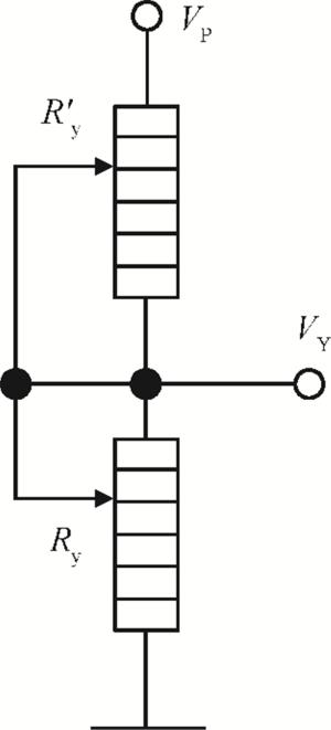
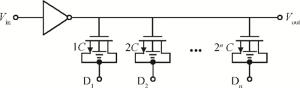
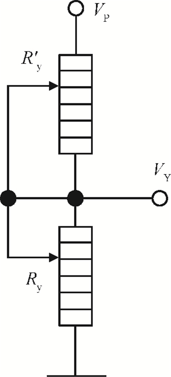
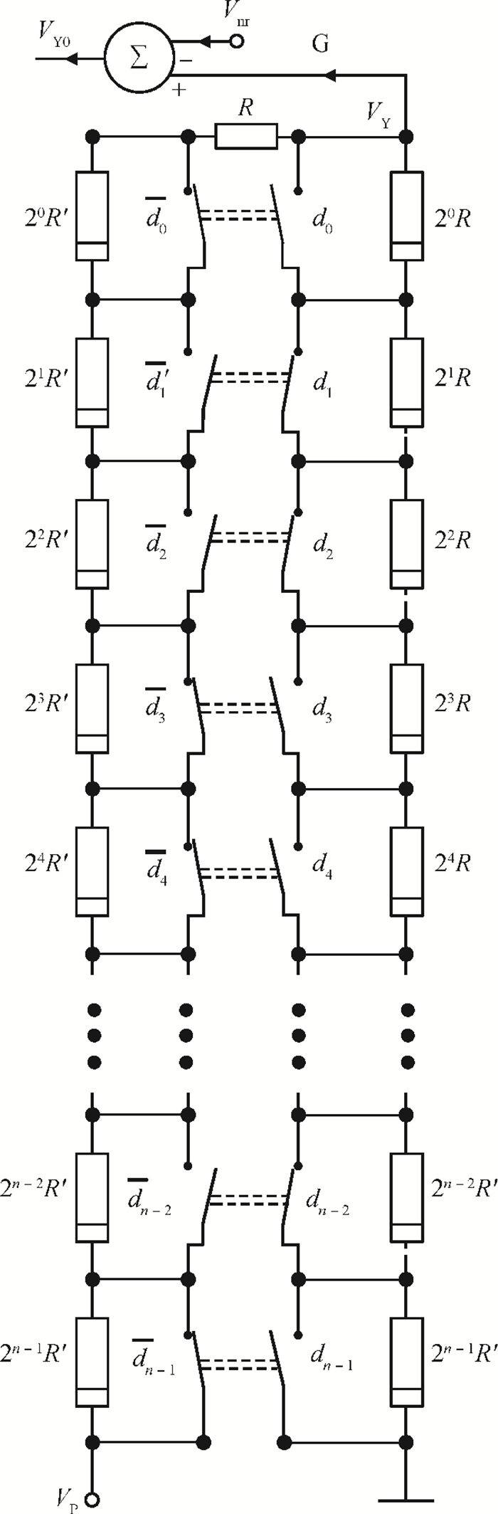
At present, the architecture of a digital-to-analog converter (DAC) in essence is based on the weight current, and the average value of its D/A signal current increases in geometric series according to its digital signal bits increase, which is 2n-1 times of its least weight current. But for a dual weight resistance chain type DAC, by using the weight voltage manner to D/A conversion, the D/A signal current is fixed to chain current Icha; it is only 1/2n-1 order of magnitude of the average signal current value of the weight current type DAC. Its principle is:n pairs dual weight resistances form a resistance chain, which ensures the constancy of the chain current; if digital signals control the total weight resistance from the output point to the zero potential point, that could directly control the total weight voltage of the output point, so that the digital signals directly turn into a sum of the weight voltage signals; thus the following goals are realized:(1) the total current is less than 200 μA; (2) the total power consumption is less than 2 mW; (3) an 18-bit conversion can be realized by adopting a multi-grade structure; (4) the chip area is one order of magnitude smaller than the subsection current-steering type DAC; (5) the error depends only on the error of the unit resistance, so it is smaller than the error of the subsection current-steering type DAC; (6) the conversion time is only one action time of switch on or off, so its speed is not lower than the present DAC.


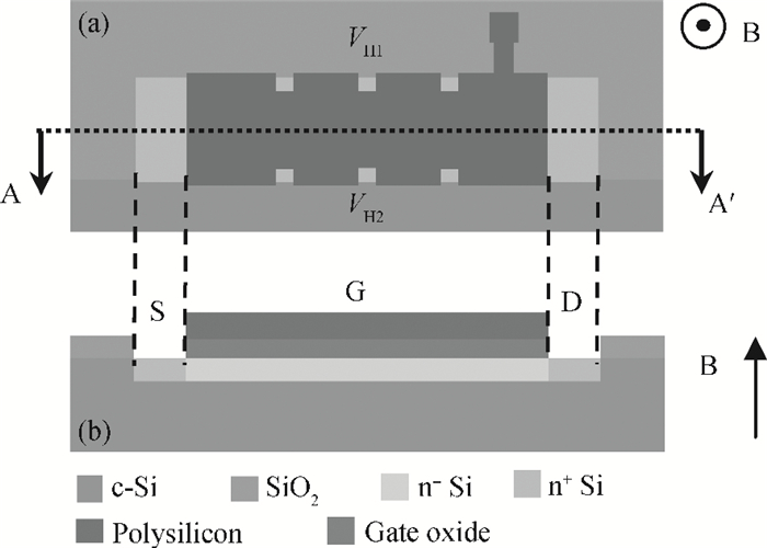
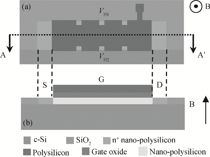
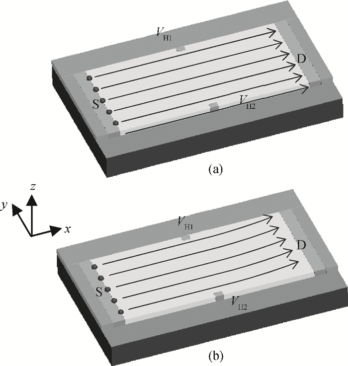
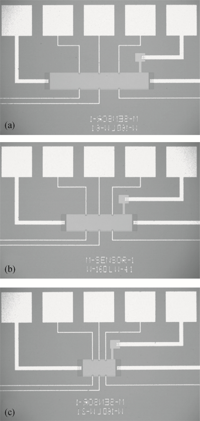
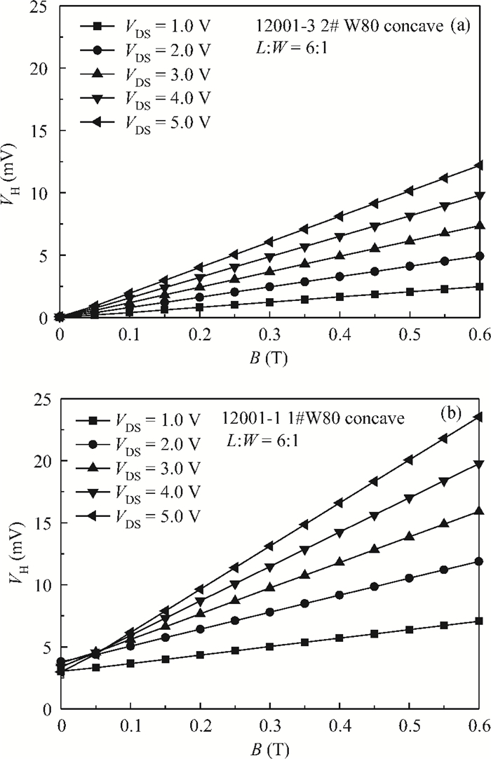
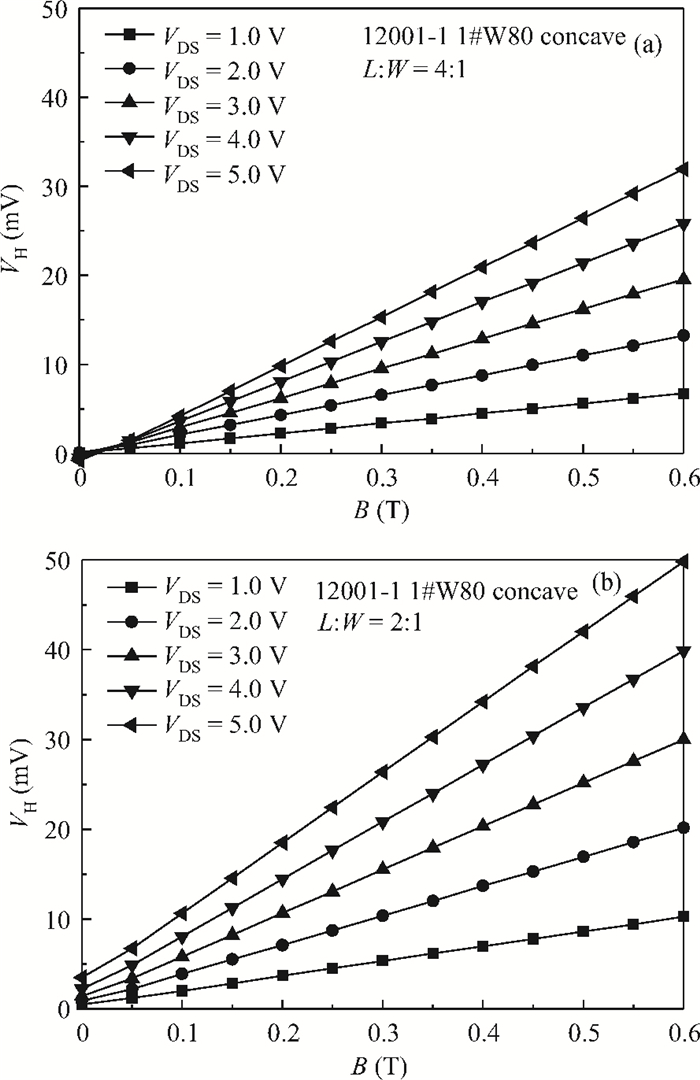
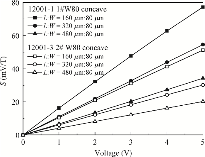
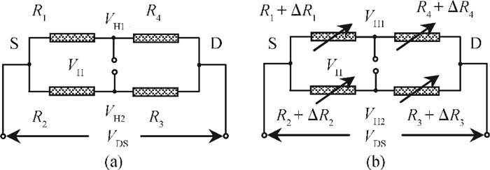
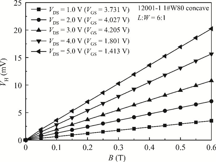
A magnetic field sensor based on nano-polysilicon thin films transistors (TFTs) with Hall probes is proposed. The magnetic field sensors are fabricated on < 100> orientation high resistivity (ρ>500 Ω·cm) silicon substrates by using CMOS technology, which adopt nano-polysilicon thin films with thicknesses of 90 nm and heterojunction interfaces between the nano-polysilicon thin films and the high resistivity silicon substrates as the sensing layers. The experimental results show that when VDS=5.0 V, the magnetic sensitivities of magnetic field sensors based on nano-polysilicon TFTs with length-width ratios of 160 μm/80 μm, 320 μm/80 μm and 480 μm/80 μm are 78 mV/T, 55 mV/T and 34 mV/T, respectively. Under the same conditions, the magnetic sensitivity of the obtained magnetic field sensor is significantly improved in comparison with a Hall magnetic field sensor adopting silicon as the sensing layers.


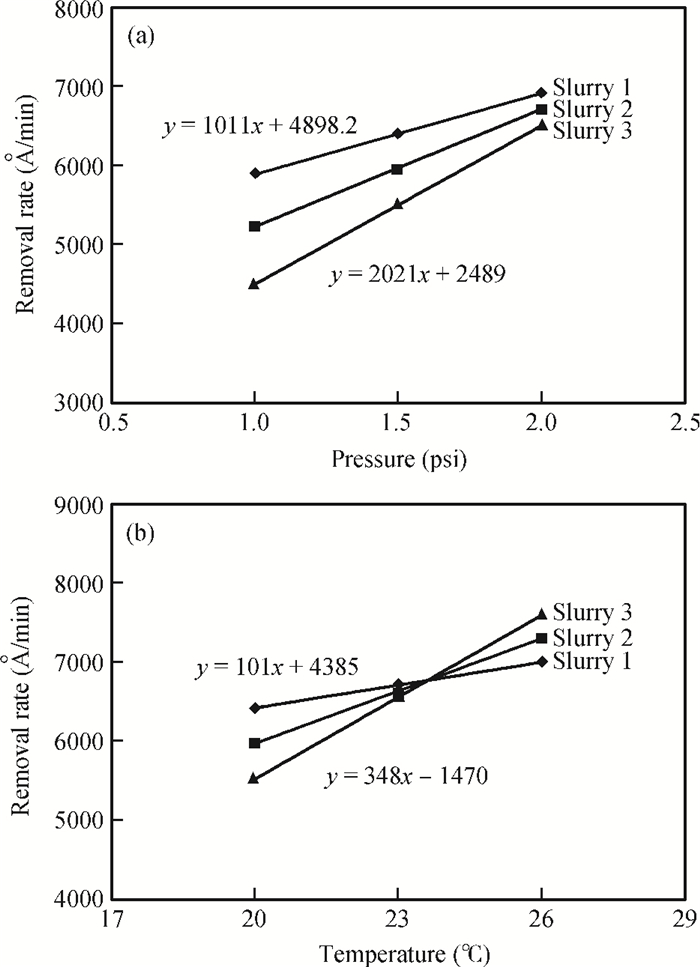
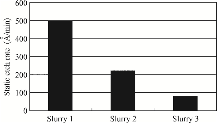
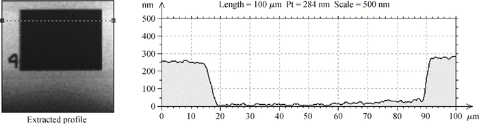
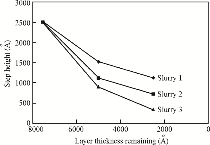
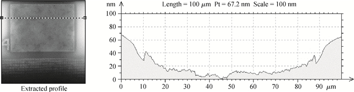
The evaluation methods of planarization capability of copper slurry are investigated. Planarization capability and material removal rate are the most essential properties of slurry. The goal of chemical mechanical polishing (CMP) is to achieve a flat and smooth surface. Planarization capability is the elimination capability of the step height on the copper pattern wafer surface, and reflects the passivation capability of the slurry to a certain extent. Through analyzing the planarization mechanism of the CMP process and experimental results, the planarization capability of the slurry can be evaluated by the following five aspects:pressure sensitivity, temperature sensitivity, static etch rate, planarization efficiency and saturation properties.