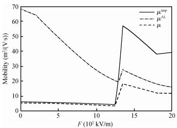
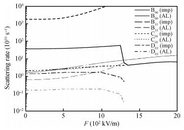
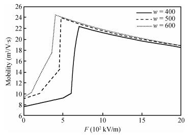
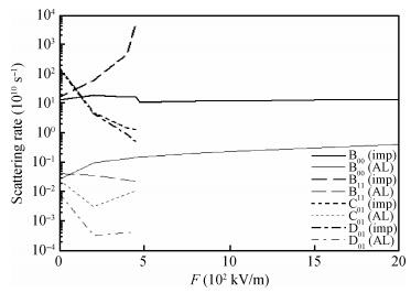
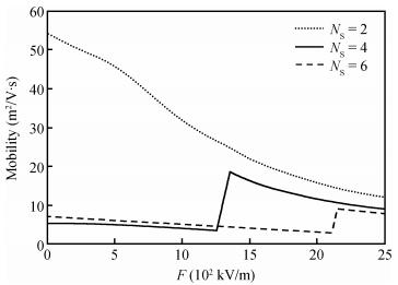
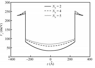
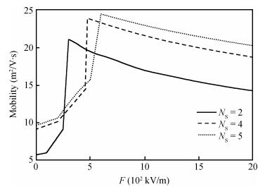
We study the multisubband electron mobility in a barrier delta doped AlxGa1-xAs parabolic quantum well structure under the influence of an applied electric field perpendicular to the interface plane. We consider the alloy fraction x=0.3 for barriers and vary x from 0.0 to 0.1 for the parabolic well. Electrons diffuse into the well and confine within the triangular like potentials near the interfaces due to Coulomb interaction with ionized donors. The parabolic structure potential, being opposite in nature, partly compensates the Coulomb potential. The external electric field further amends the potential structure leading to an asymmetric potential profile. Accordingly the energy levels, wave functions and occupation of subbands change. We calculate low temperature electron mobility as a function of the electric field and show that when two subbands are occupied, the mobility is mostly dominated by ionised impurity scattering mediated by intersubband effects. As the field increases transition from double subband to single subband occupancy occurs. A sudden enhancement in mobility is obtained due to curtailment of intersubband effects. Thereafter the mobility is governed by both impurity and alloy disorder scatterings. Our analysis of mobility as a function of the electric field for different structural parameters shows interesting results.


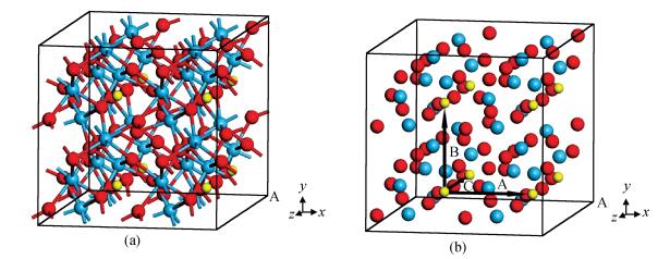
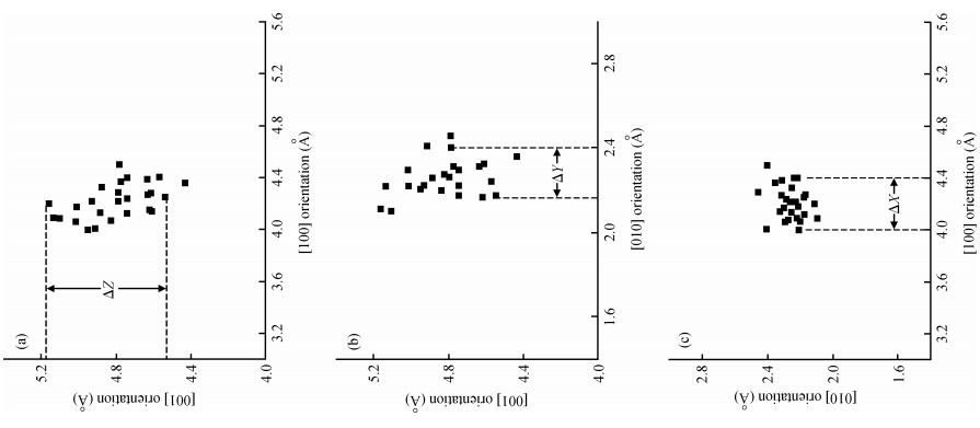
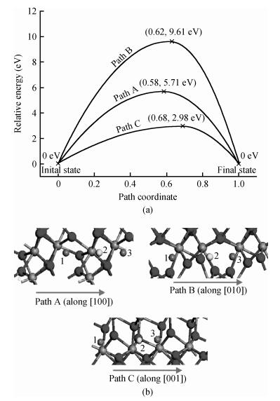
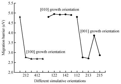
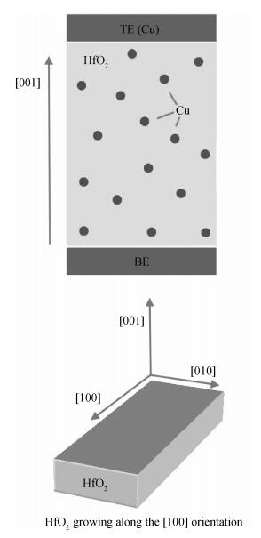
The movement of Cu in a HfO2-based resistive random access memory (RRAM) device is investigated in depth by first-principle calculations. Thermodynamics analysis shows that the dominant motion of Cu tends to be along the[001] orientation with a faster speed. The migration barriers along different routes are compared and reveal that the[001] orientation is the optimal migration route of Cu in HfO2, which is more favorable for Cu transportation. Furthermore, the preferable HfO2 growth orientation along[100], corresponding to Cu migration along[001], is also observed. Therefore, it is proposed that the HfO2 material should grow along[100] and the operating voltage should be applied along[001], which will contribute to the improvement of the response speed and the reduction of power consumption of RRAM.


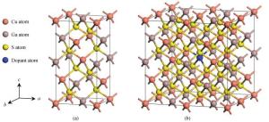
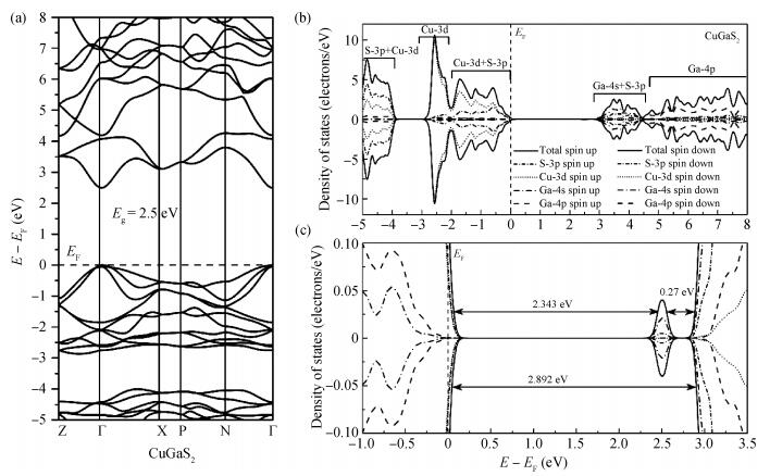
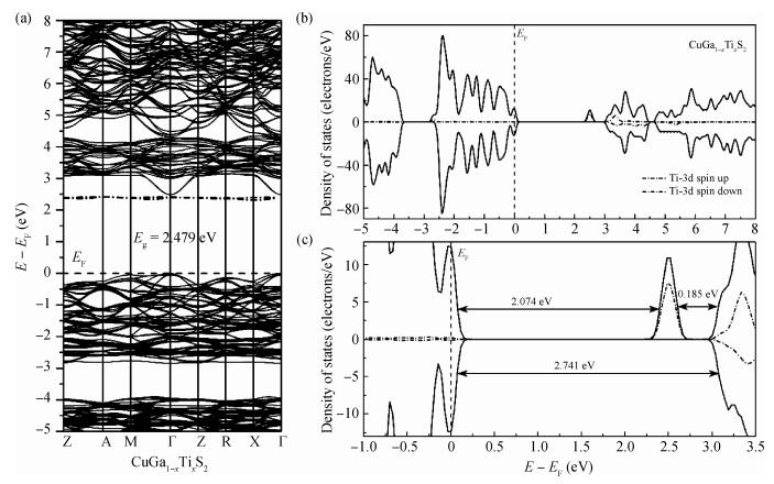
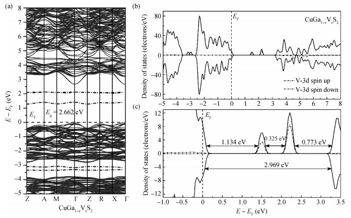
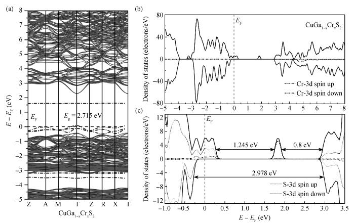
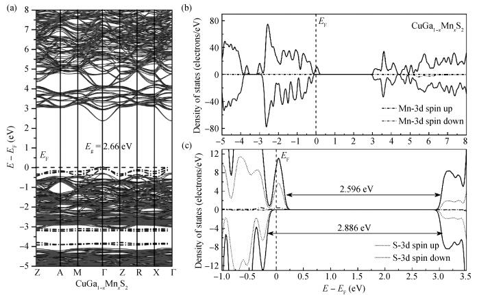
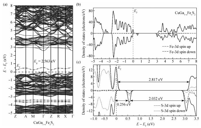
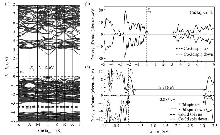
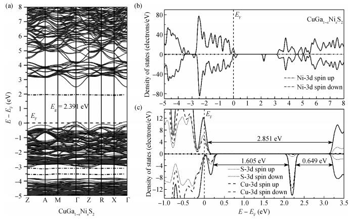
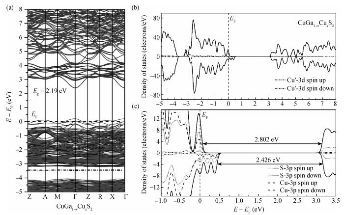
3d transition metals doped CuGaS2 are considered as possible absorbing material candidates for intermediated band thin film solar cells. The electronic structure and optical properties of 3d transition metals doped CuGaS2 are investigated by using density functional theory calculations with the GGA + U method in the present work. The doping with 3d transition metals does not obviously change the crystal structure, band gap, and optical absorption edge of the CuGaS2 host. However, in the case of CuGa1-xTMxS2 (TM=Ti, V, Cr, Fe, and Ni), there is at least one distinct isolated impurity energy level in the band gap, and the optical absorption is enhanced in the ultraviolet-light region. Therefore, these materials are ideal absorber material candidates for intermediated band thin film solar cells. The calculated results are very well consistent with experimental observations, and could better explain them.


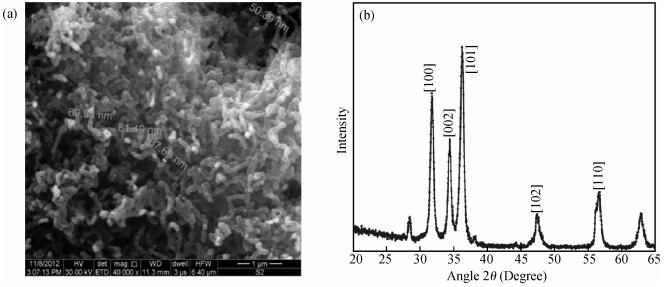
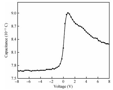
This paper represents the electrical and optical characteristics of a SiNW/ZnO heterojunction diode and subsequent studies on the photodetection properties of the diode in the ultraviolet (UV) wavelength region. In this work, silicon nanowire arrays were prepared on p-type (100)-oriented Si substrate by an electroless metal deposition and etching method with the help of ultrasonication. After that, catalyst-free deposition of zinc oxide (ZnO) nanowires on a silicon nanowire (SiNW) array substrate was done by utilizing a simple and cost-effective thermal evaporation technique without using a buffer layer. The SEM and XRD techniques are used to show the quality of the as-grown ZnO nanowire film. The junction properties of the diode are evaluated by measuring current-voltage and capacitance-voltage characteristics. The diode has a well-defined rectifying behavior with a rectification ratio of 190 at ±2 V, turn-on voltage of 0.5 V, and barrier height is 0.727 eV at room temperature under dark conditions. The photodetection parameters of the diode are investigated in the bias voltage range of ±2 V. The diode shows responsivity of 0.8 A/W at a bias voltage of 2 V under UV illumination (wavelength=365 nm). The characteristics of the device indicate that it can be used for UV detection applications in nano-optoelectronic and photonic devices.


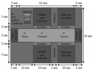
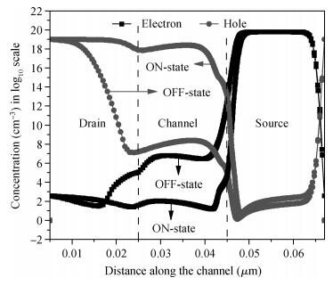
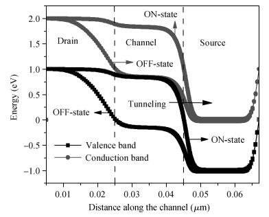
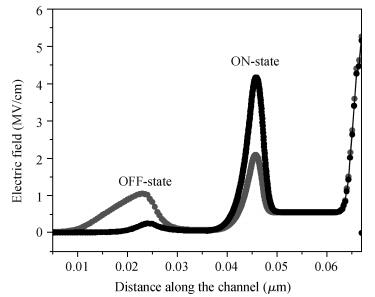
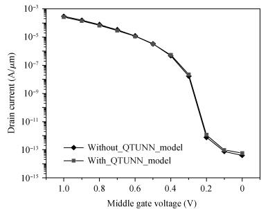
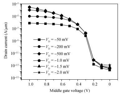
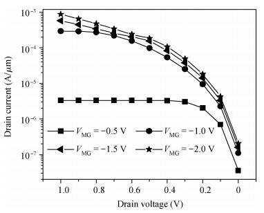
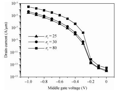
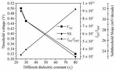
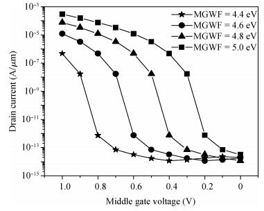
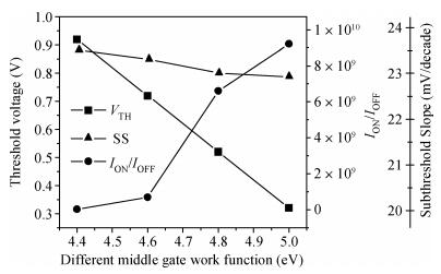
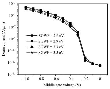
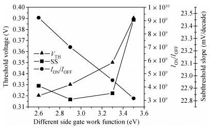
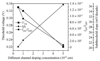
We have investigated the 20 nm p-type double gate junctionless tunnel field effect transistor (P-DGJLTFET) and the impact of variation of different device parameters on the performance parameters of the P-DGJLTFET is discussed. We achieved excellent results of different performance parameters by taking the optimized device parameters of the P-DGJLTFET. Together with a high-k dielectric material (TiO2) of 20 nm gate length, the simulation results of the P-DGJLTFET show excellent characteristics with a high ION of 0.3 mA/μm, a low IOFF of 30 fA/μm, a high ION/IOFF ratio of 1×10¹⁰, a subthreshold slope (SS) point of 23 mV/decade, and an average SS of 49 mV/decade at a supply voltage of -1 V and at room temperature, which indicates that P-DGJLTFET is a promising candidate for sub-22 nm technology nodes in the implementation of integrated circuits.


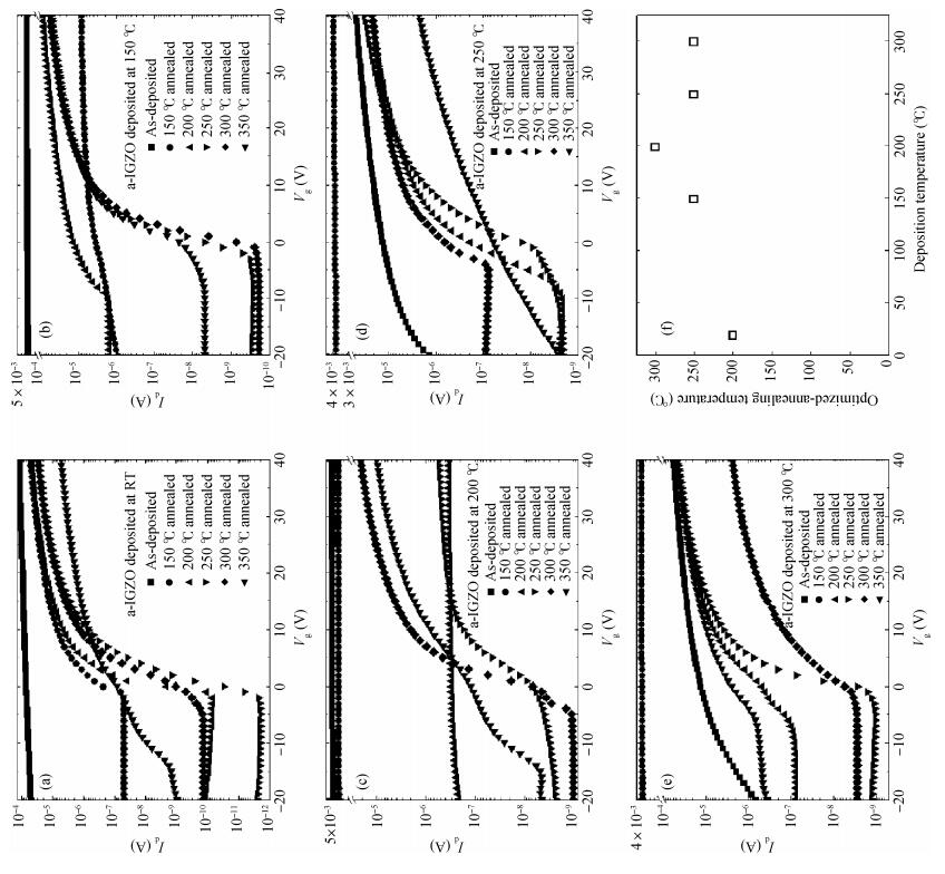
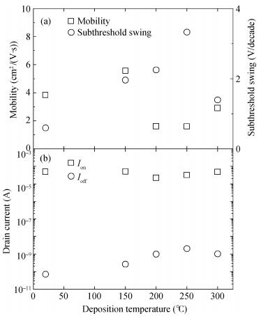
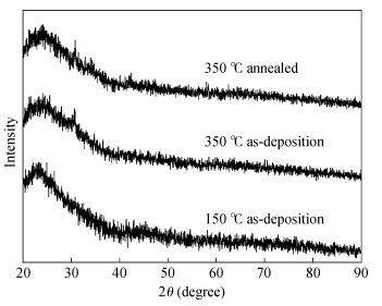
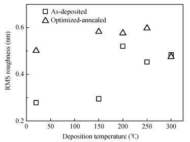
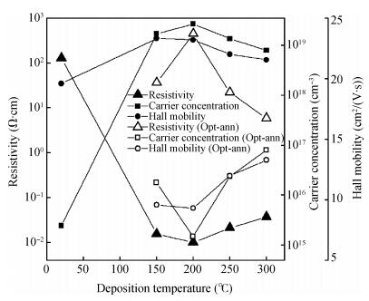
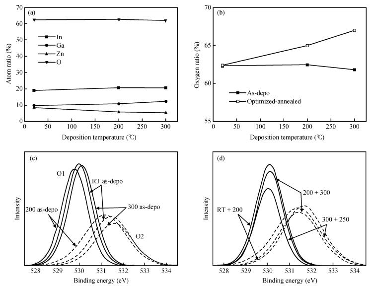
The effect of active layer deposition temperature on the electrical performance of amorphous InGaZnO (a-IGZO) thin film transistors (TFTs) is investigated. With increasing annealing temperature, TFT performance is firstly improved and then degraded generally. Here TFTs with best performance defined as "optimized-annealed" are selected to study the effect of active layer deposition temperature. The field effect mobility reaches maximum at deposition temperature of 150℃ while the room-temperature fabricated device shows the best subthreshold swing and off-current. From Hall measurement results, the carrier concentration is much higher for intentional heated a-IGZO films, which may account for the high off-current in the corresponding TFT devices. XPS characterization results also reveal that deposition temperature affects the atomic ratio and O1s spectra apparently. Importantly, the variation of field effect mobility of a-IGZO TFTs with deposition temperature does not coincide with the tendencies in Hall mobility of a-IGZO thin films. Based on the further analysis of the experimental results on a-IGZO thin films and the corresponding TFT devices, the trap states at front channel interface rather than IGZO bulk layer properties may be mainly responsible for the variations of field effect mobility and subthreshold swing with IGZO deposition temperature.
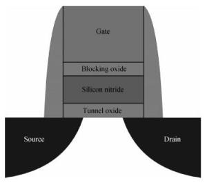
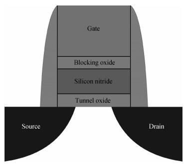
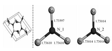
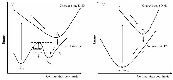
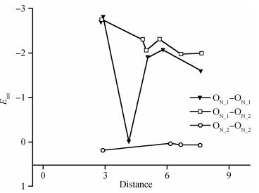
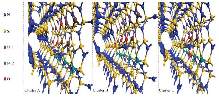
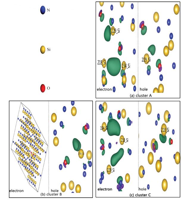
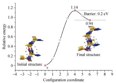
Based on first principle calculations, a comprehensive study of substitutional oxygen defects in hexagonal silicon nitride (β-Si3N4) has been carried out. Firstly, it is found that substitutional oxygen is most likely to form clusters at three sites in Si3N4 due to the intense attractive interaction between oxygen defects. Then, by using three analytical tools (trap energy, modified Bader analysis and charge density difference), we discuss the trap abilities of the three clusters. The result shows that each kind of cluster at the three specific sites presents very different abilities to trap charge carriers (electrons or holes):two of the three clusters can trap both kinds of charge carriers, confirming their amphoteric property; While the last remaining one is only able to trap hole carriers. Moreover, our studies reveal that the three clusters differ from each other in terms of endurance during the program/erase progress. Taking full account of capturing properties for the three oxygen clusters, including trap ability and endurance, we deem holes rather than electrons to be optimal to act as operational charge carriers for the oxygen defects in Si3N4-based charge trapping memories.


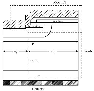
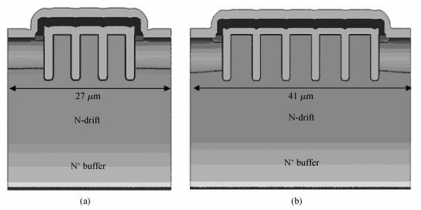
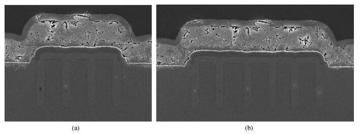
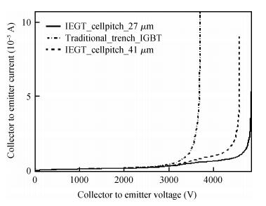
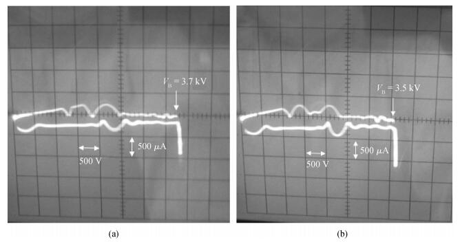
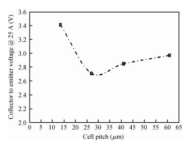
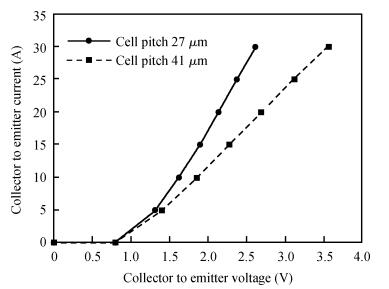
This paper introduces a homemade injection-enhanced gate transistor (IEGT) with blocking voltage up to 3.7 kV. An advanced cell structure with dummy trench and a large cell pitch is adopted in the IEGT. The carrier concentration at the N-emitter side is increased by the larger cell pitch of the IEGT and it enhances the P-i-N effect within the device. The result shows that the IEGT has a remarkablely low on-state forward voltage drop (VCE(sat)) compared to traditional trench IGBT structures. However, too large cell pitch decreases the channel density of the trench IEGT and increases the voltage drop across the channel, finally it will increase the VCE(sat) of the IEGT. Therefore, the cell pitch selection is the key parameter consideration in the design of the IEGT. In this paper, a cell pitch selection method and the optimal value of 3.3 kV IEGT are presented by simulations and experimental results.

A vertical two-terminal silicon PNPN diode is presented for use in a high-density memory cell. The device design for high-speed operations was studied with experiments and calibrated simulations, which proves that the proposed memory cell can be operated at nanosecond range. The static and dynamic power dissipations were also studied, which indicated the availability of the proposed memory cell for VLSI applications. Moreover, the memory cell is compatible with CMOS process, has little impact from process variation, and has good reliability.


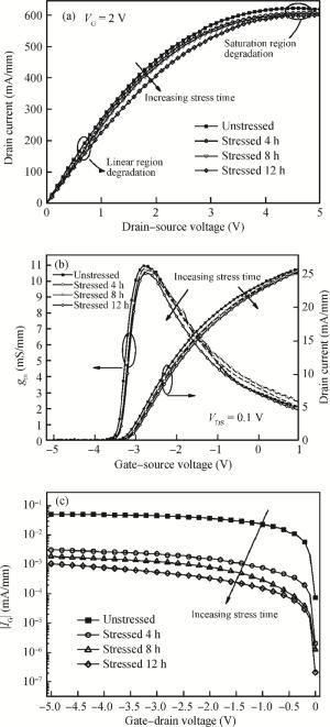
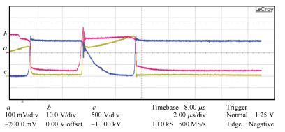
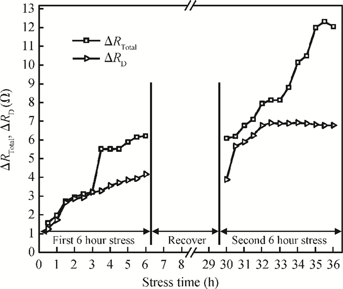
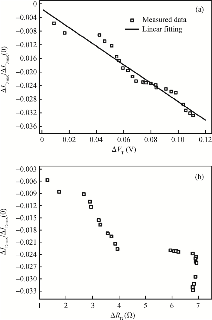
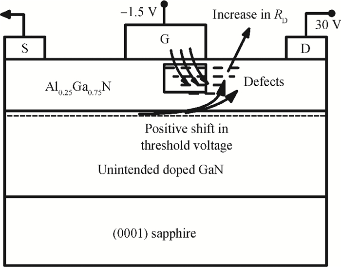
Semi-on DC stress experiments were conducted on AlGaN/GaN high electron mobility transistors (HEMTs) to find the degradation mechanisms during stress. A positive shift in threshold voltage (VT) and an increase in drain series resistance (RD) were observed after semi-on DC stress on the tested HEMTs. It was found that there exists a close correlation between the degree of drain current degradation and the variation in VT and RD. Our analysis shows that the variation in VT is the main factor leading to the degradation of saturation drain current (IDS), while the increase in RD results in the initial degradation of IDS in linear region in the initial several hours stress time and then the degradation of VT plays more important role. Based on brief analysis, the electron trapping effect induced by gate leakage and the hot electron effect are ascribed to the degradation of drain current during semi-on DC stress. We suggest that electrons in the gate current captured by the traps in the AlGaN layer under the gate metal result in the positive shift in VT and the trapping effect in the gate-drain access region induced by the hot electron effect accounts for the increase in RD.

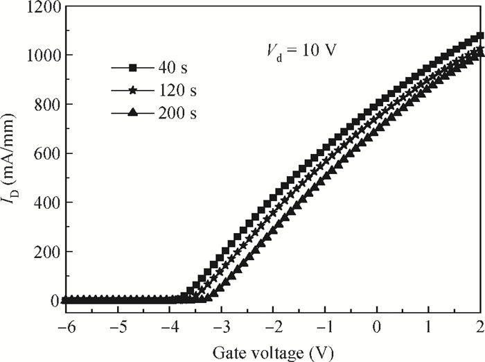
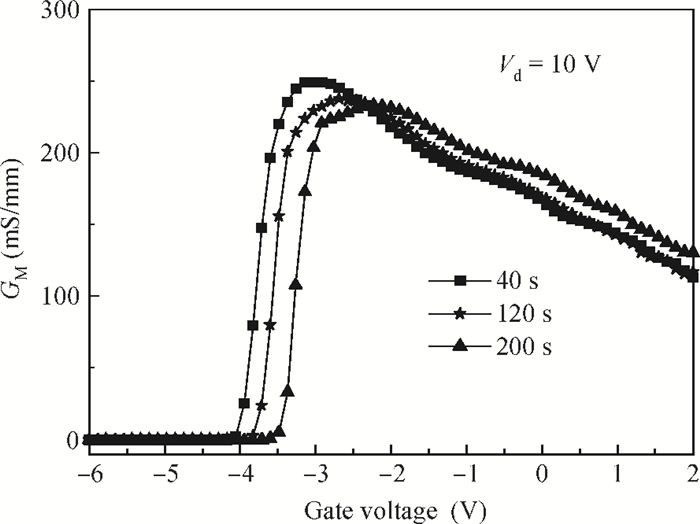
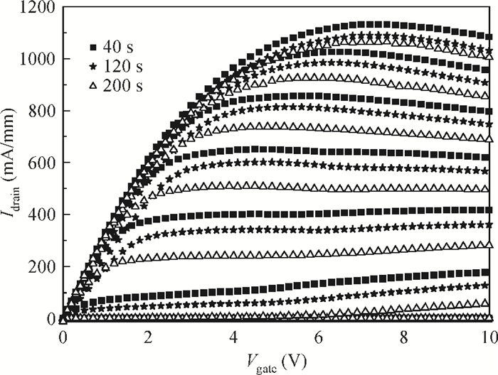
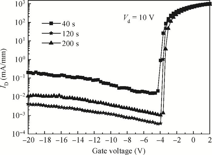
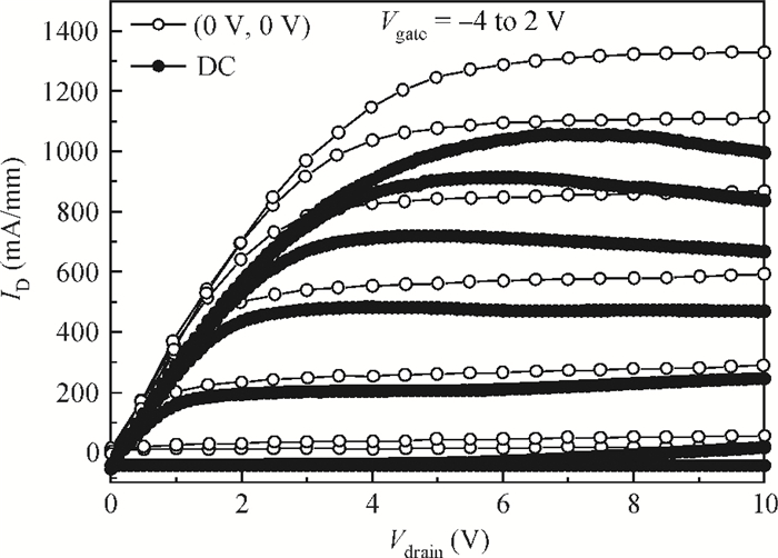
The breakdown and the current collapse characteristics of high electron mobility transistors (HEMTs) with a low power F-plasma treatment process are investigated. With the increase of F-plasma treatment time, the saturation current decreases, and the threshold voltage shifts to the positive slightly. Through analysis of the Schottky characteristics of the devices with different F-plasma treatment times, it was found that an optimal F-plasma treatment time of 120 s obviously reduced the gate reverse leakage current and improved the breakdown voltage of the devices, but longer F-plasma treatment time than 120 s did not reduce gate reverse leakage current due to plasma damage. The current collapse characteristics of the HEMTs with F-plasma treatment were evaluated by dual pulse measurement at different bias voltages and no obvious deterioration of current collapse were found after low power F-plasma treatment.


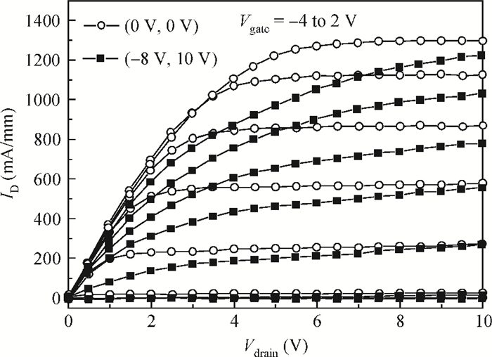
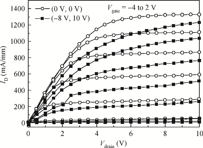

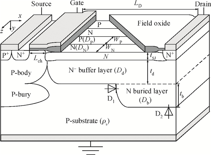
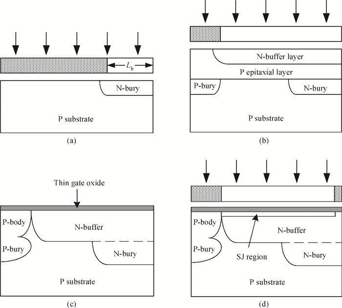
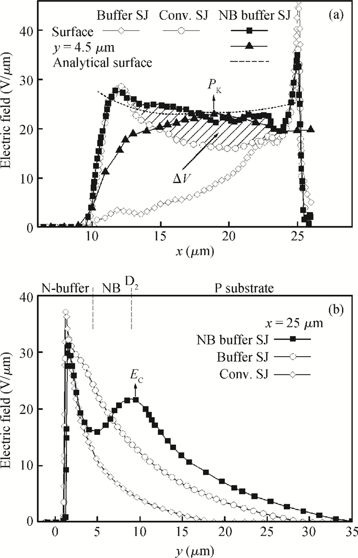
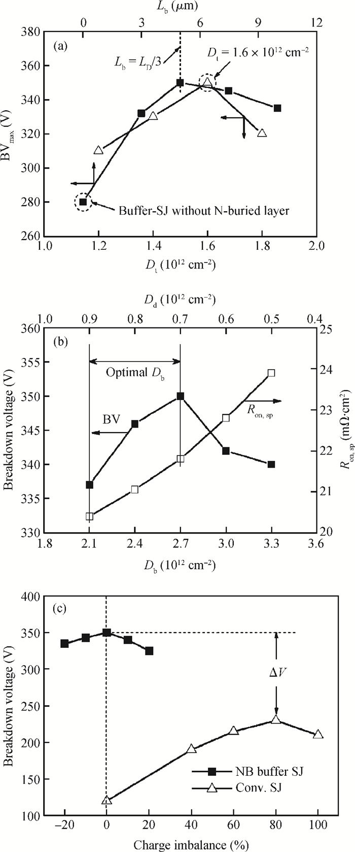
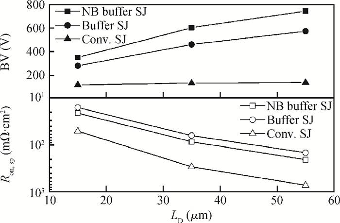
A novel buffer super-junction (SJ) lateral double-diffused MOSFET (LDMOS) with an N-type buried layer (NB) is proposed. An N- buffer layer is implemented under the SJ region and an N-type layer is buried in the P substrate. Firstly, the new electric field peak introduced by the p-n junction of the P substrate and the N-type buried layer modulates the surface electric field distribution. Secondly, the N- buffer layer suppresses the substrate assisted depletion effect. Both of them improve the breakdown voltage (BV). Finally, because of the shallow depth of the SJ region, the NB buffer SJ-LDMOS is compatible with Bi-CMOS technology. Simulation results indicate that the average value of the surface lateral electric field strength of the NB buffer SJ-LDMOS reaches 23 V/μm at 15 μm drift length which results in a BV of 350 V and a specific on-resistance of 21 mΩ · cm2.

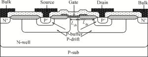
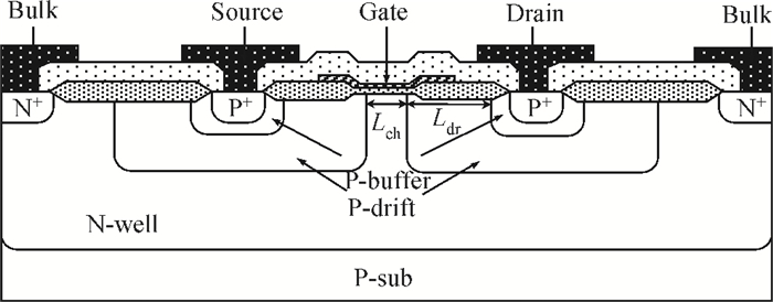
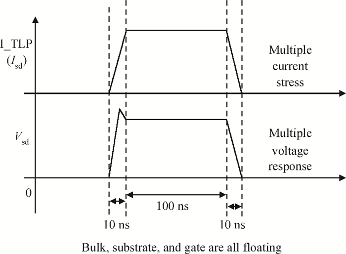
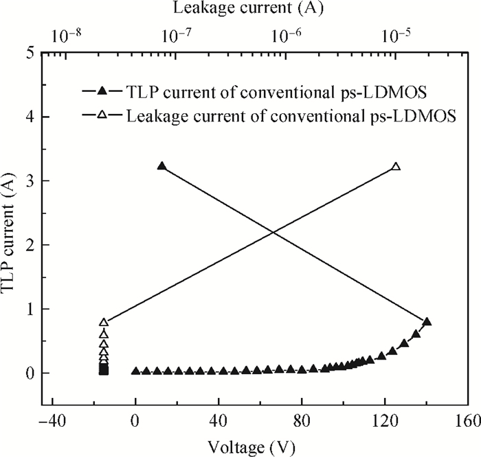
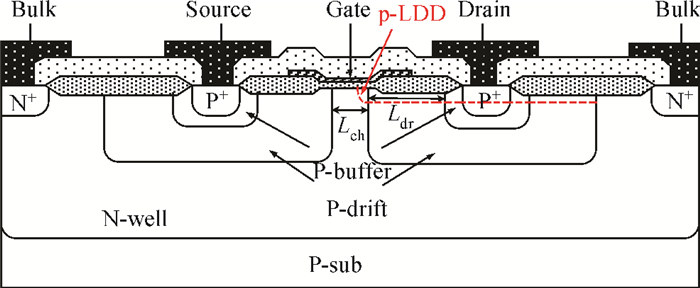
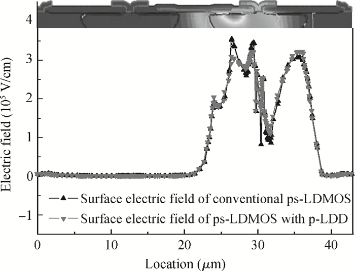
The ESD response characteristic in a p-type symmetric lateral DMOS (ps-LDMOS) has been investigated. The experimental results show that the ps-LDMOS has weak ESD robustness due to an absence of the "snapback" characteristic. In addition, the location of the hot spot changes little for the special device. The method for reducing the lattice temperature of the hot spot can be used to enhance the ESD capacity of the ps-LDMOS, thereby, a novel and easily-achievable ps-LDMOS structure with a p-type lightly doped drain (p-LDD) has been proposed. The special region p-LDD lowers the electric field at the edge of the poly gate, making the whole distribution of the surface electric field more uniform. Therefore, the ESD robustness is improved two times and no obvious change of other electric parameters is introduced.


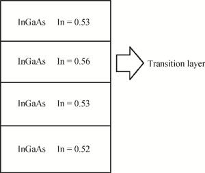
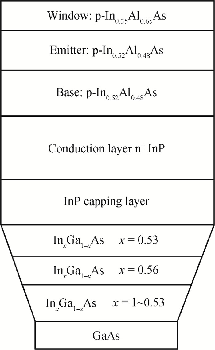
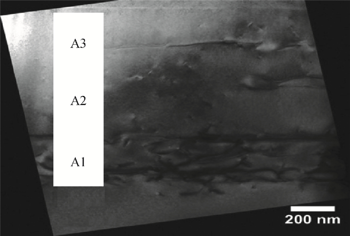
This paper uses an InGaAs graded buffer layer to solve the problem of lattice mismatch and device performance degradation. In the graded buffer layer, we choose the "transition layer" and the "cover layer" to accommodate the 3.9% mismatch. No threading dislocations were observed in the uppermost part of the epitaxial layer stack when using a transmission electron microscope (TEM). We analyze the factors which influence the saturation current. Simulation data shows that the cells grown by metal organic vapor phase epitaxy (MOVPE) have considerable open circuit voltage, short circuit current, and photoelectric conversion efficiency. Finally we propose that InP may have great development potential as a substrate material.


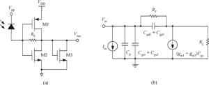
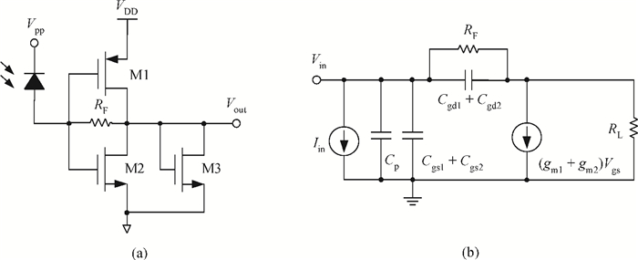
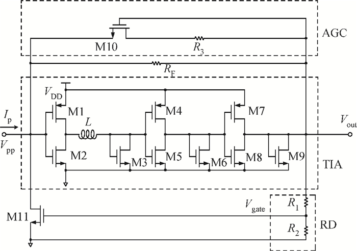
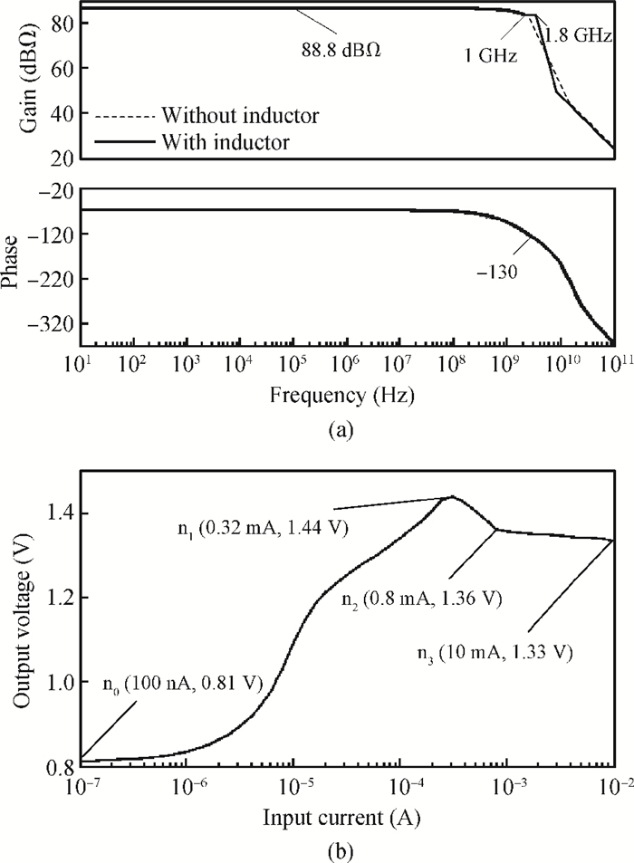
As the front-end preamplifiers in optical receivers, transimpedance amplifiers (TIAs) are commonly required to have a high gain and low input noise to amplify the weak and susceptible input signal. At the same time, the TIAs should possess a wide dynamic range (DR) to prevent the circuit from becoming saturated by high input currents. Based on the above, this paper presents a CMOS transimpedance amplifier with high gain and a wide DR for 2.5 Gbit/s communications. The TIA proposed consists of a three-stage cascade pull push inverter, an automatic gain control circuit, and a shunt transistor controlled by the resistive divider. The inductive-series peaking technique is used to further extend the bandwidth. The TIA proposed displays a maximum transimpedance gain of 88.3 dBΩ with the -3 dB bandwidth of 1.8 GHz, exhibits an input current dynamic range from 100 nA to 10 mA. The output voltage noise is less than 48.23 nV/$\sqrt {{\rm{Hz}}}$ within the -3 dB bandwidth. The circuit is fabricated using an SMIC 0.18 μm 1P6M RFCMOS process and dissipates a dc power of 9.4 mW with 1.8 V supply voltage.

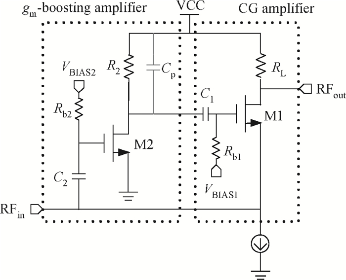
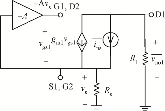
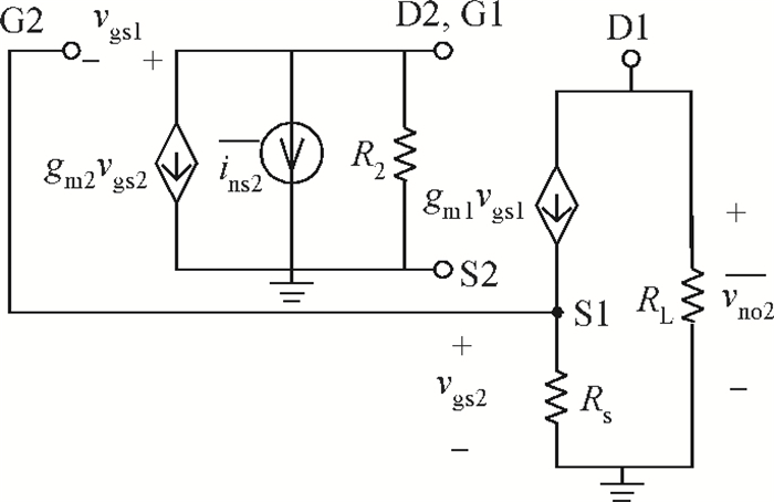
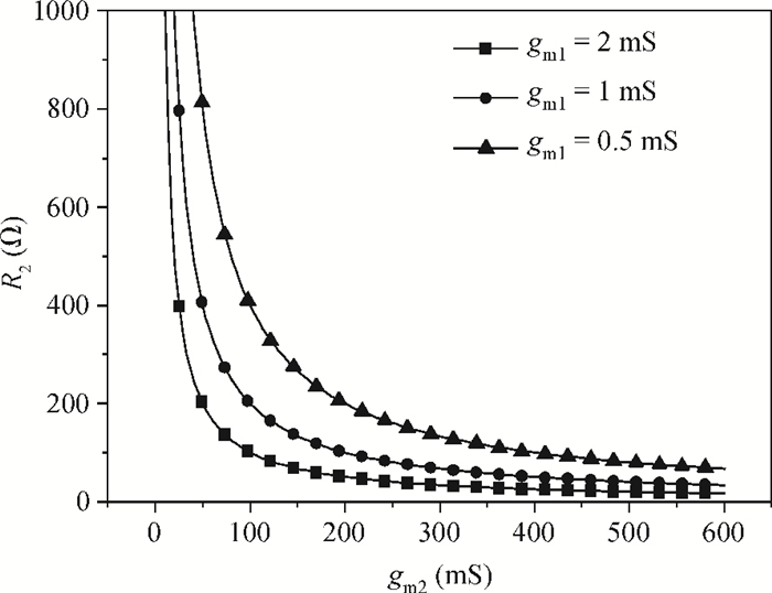
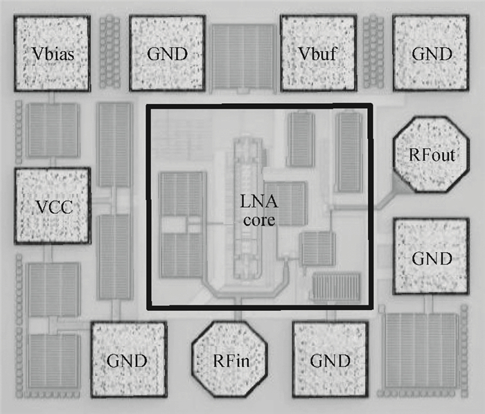
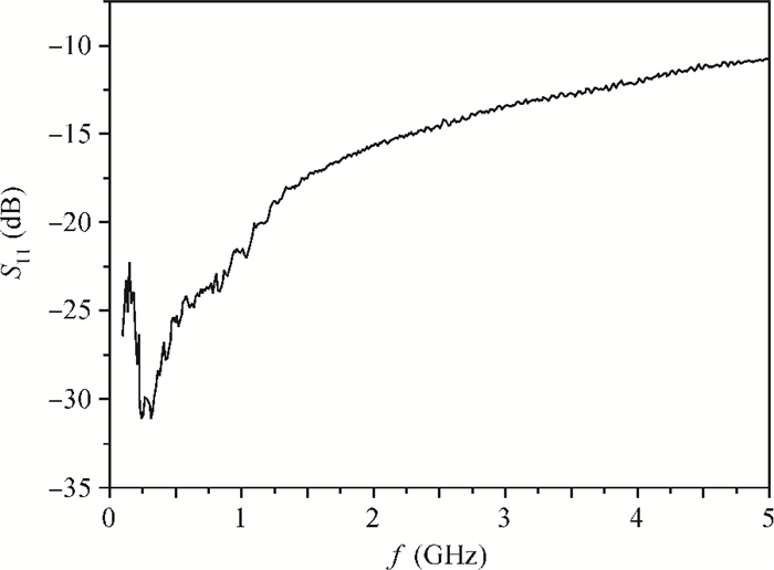
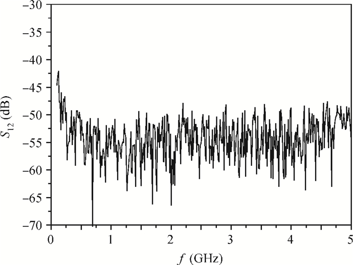
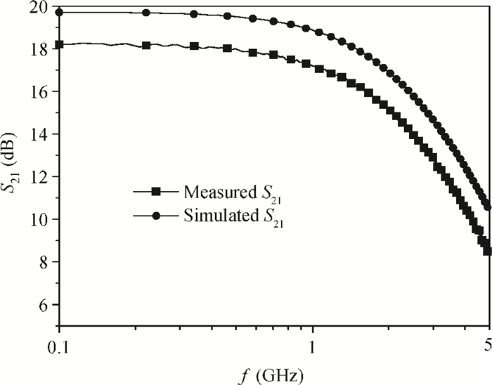
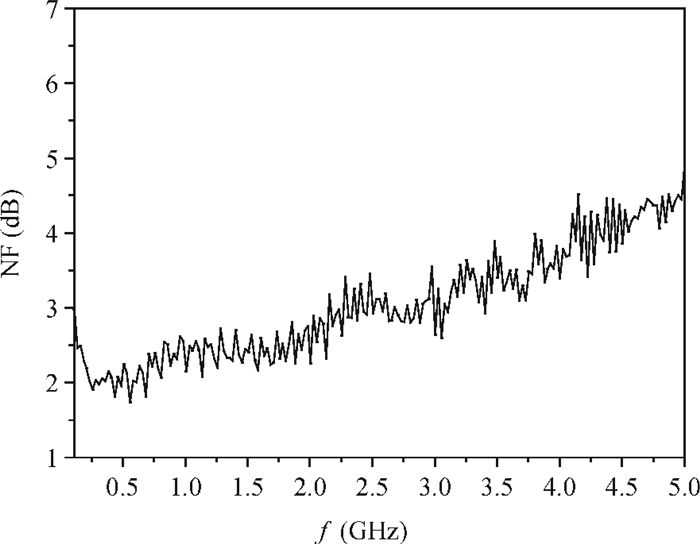
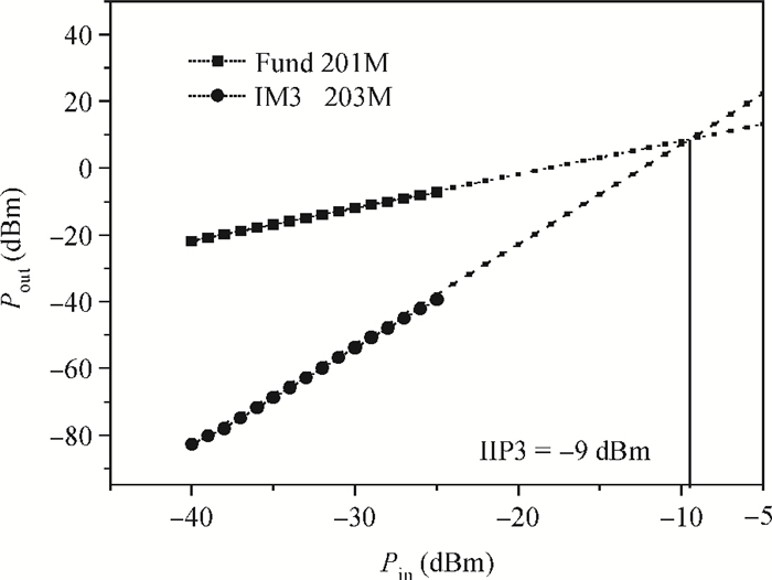
A new broadband low-noise amplifier (LNA) is proposed. The conventional common gate (CG) LNA exhibits a relatively high noise figure, so active gm-boosting technology is utilized to restrain the noise generated by the input transistors and reduce the noise figure. Theory, simulation and measurement are shown. An implemented prototype using 0.13 μm CMOS technology is evaluated using on-wafer probing. S11 and S22 are below -10 dB across 0.1-5 GHz. Measurements also show a gain of 18.3 dB with a 3 dB bandwidth from 100 MHz to 2.1 GHz and an ⅡP3 of -7 dBm at 2 GHz. The measured noise figure is better than 2.5 dB below 2.1 GHz, is better than 4.5 dB below 5 GHz, and at 500 MHz, it gets its minimum value 1.8 dB. The LNA consumes 9 mA from 1.5 V supply and occupies an area of 0.04 mm2.


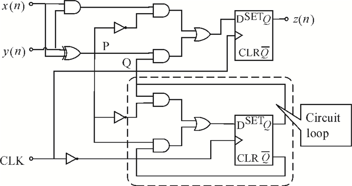
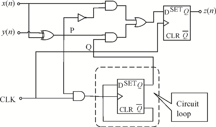
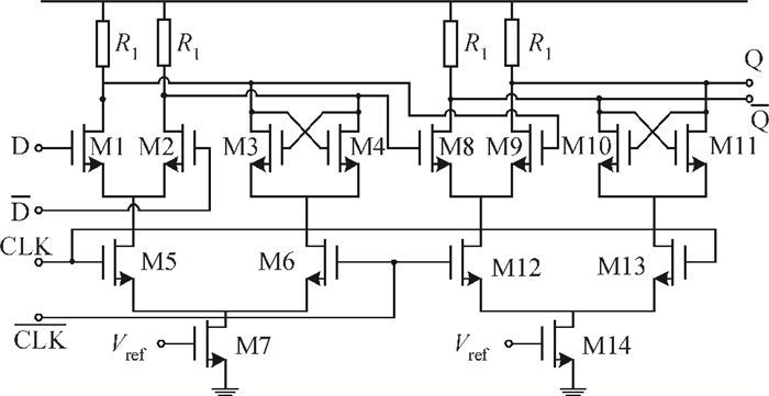
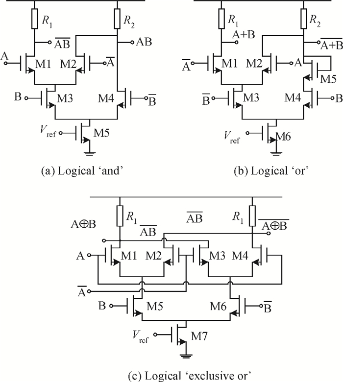
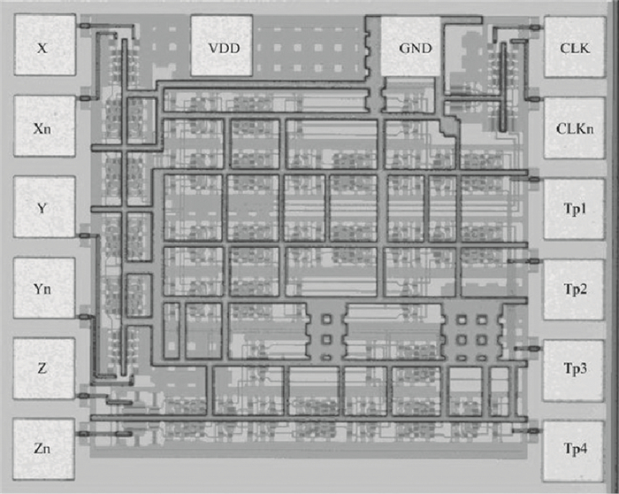
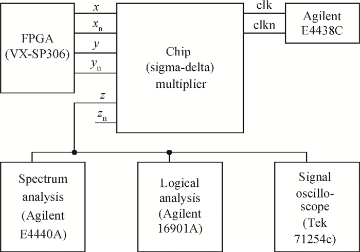
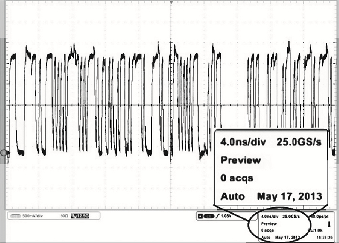
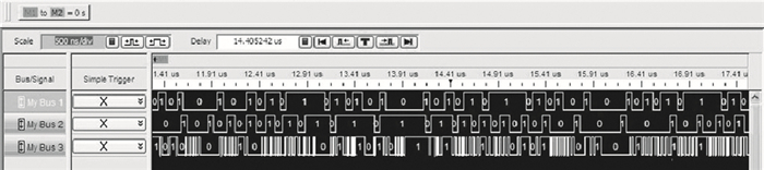
An integrated circuit design of a high speed multiplier for direct sigma-delta modulated bit-stream signals is presented. Compared with conventional structures, this multiplier reduces the circuit-loop delay of its sub-modules and works efficiently at a high speed. The multiplier's stability has also been improved with source coupled logic technology. The chip is fabricated in a TSMC 0.18-μm CMOS process. The test results demonstrate that the chip realizes the multiplication function and exhibits an excellent performance. It can work at 4 GHz and the voltage output amplitude reaches the designed maximum value with no error bit caused by logic race-and-hazard. Additionally, the analysis of the multiplier's noise performance is also presented.


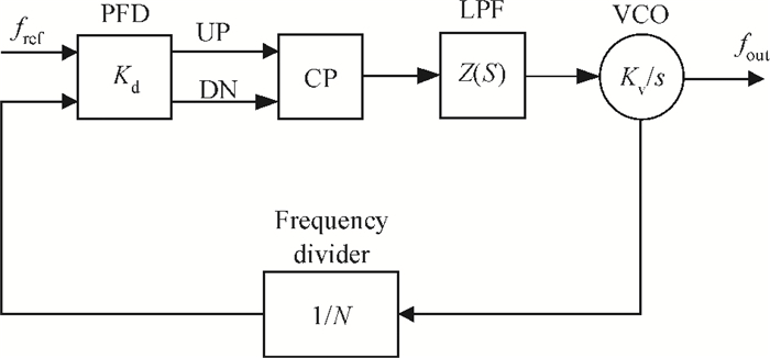
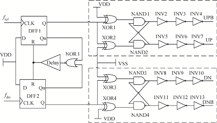
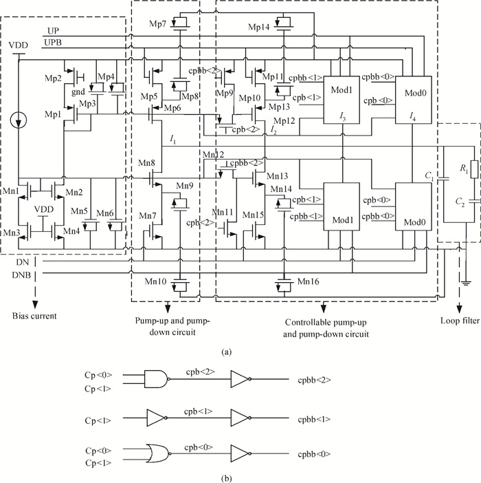
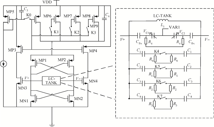
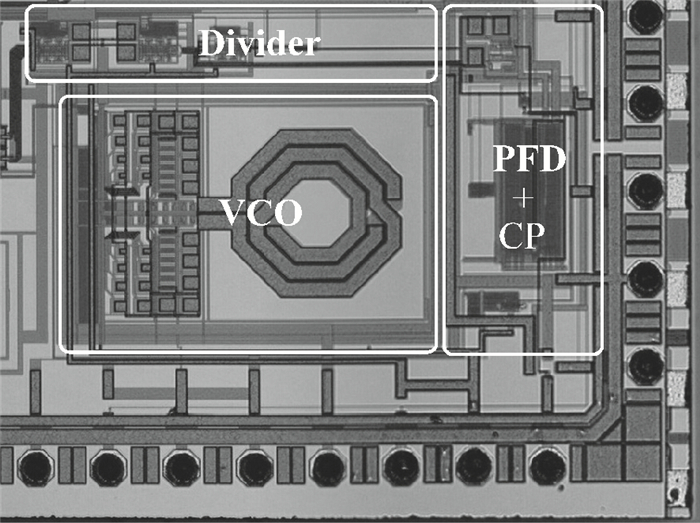
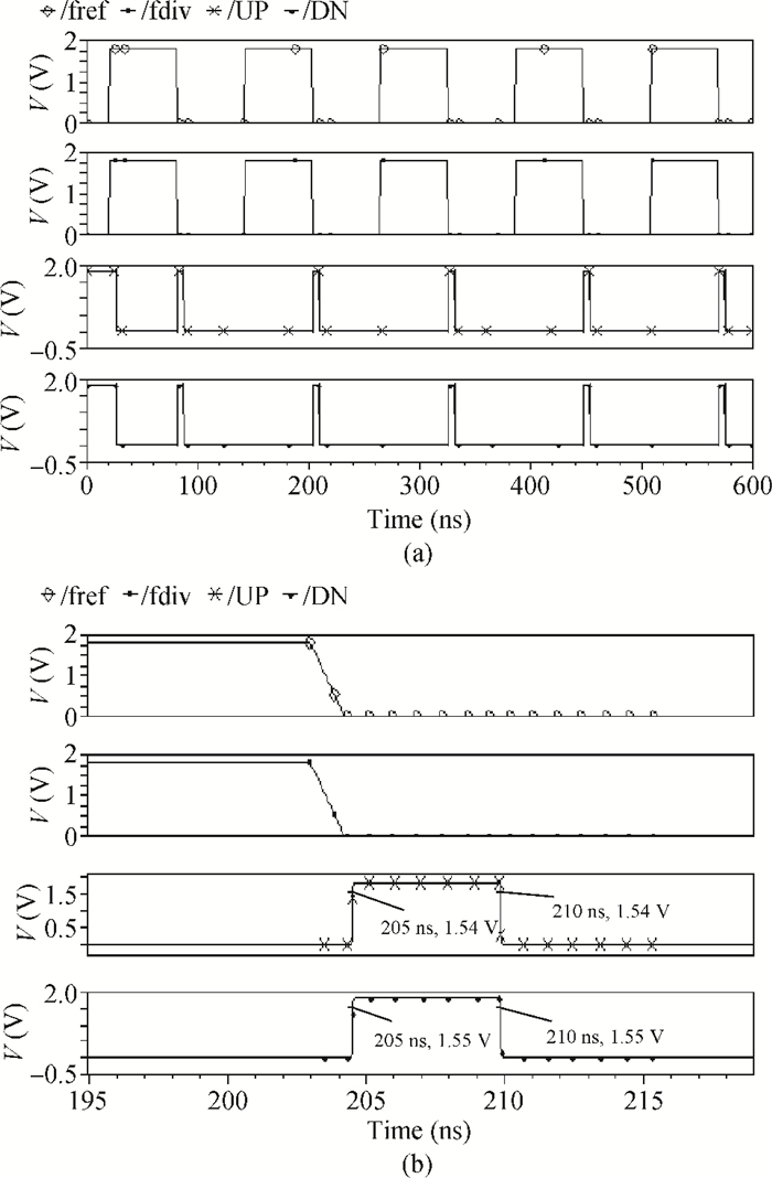
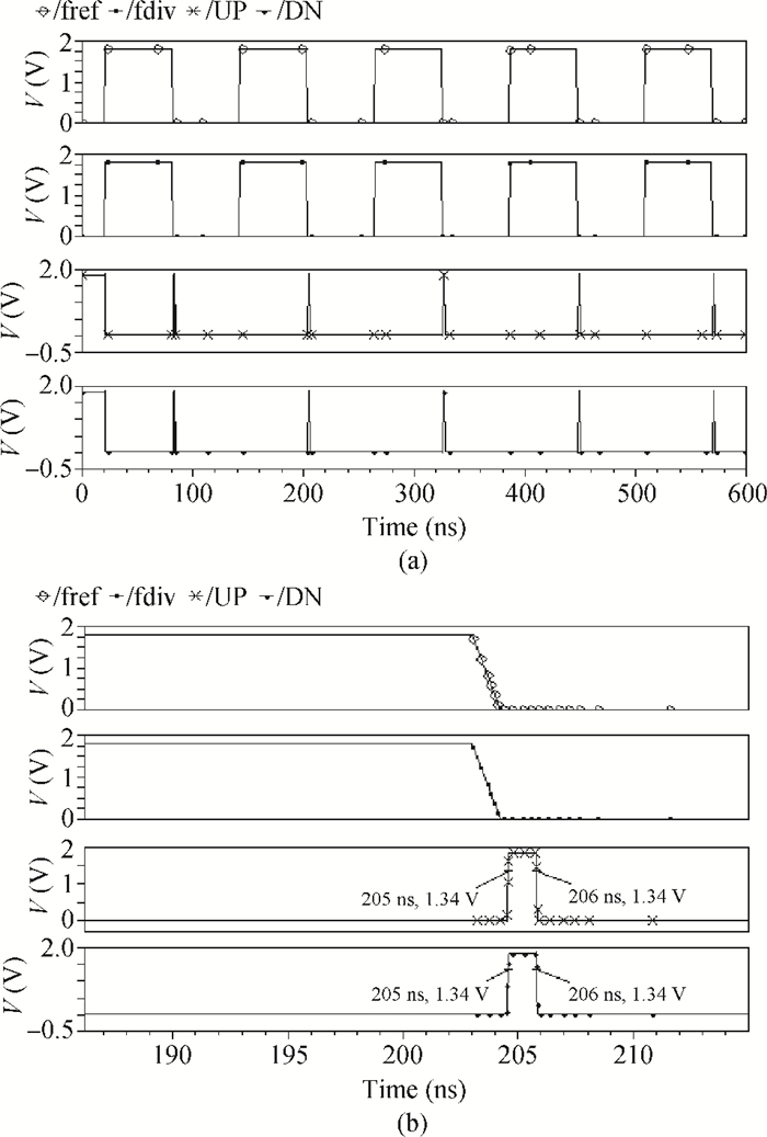
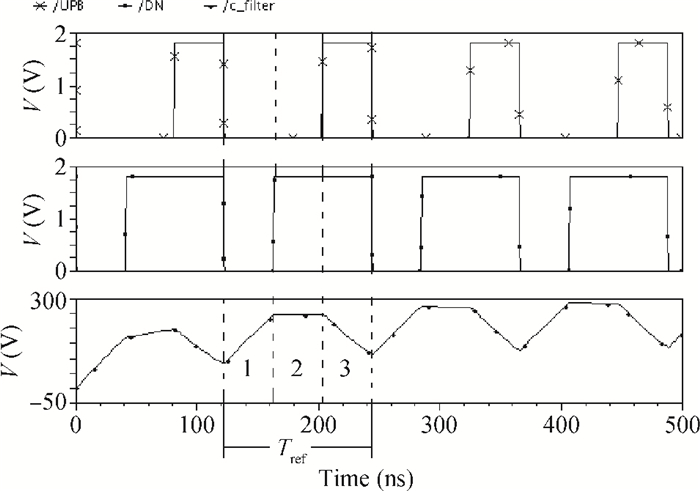
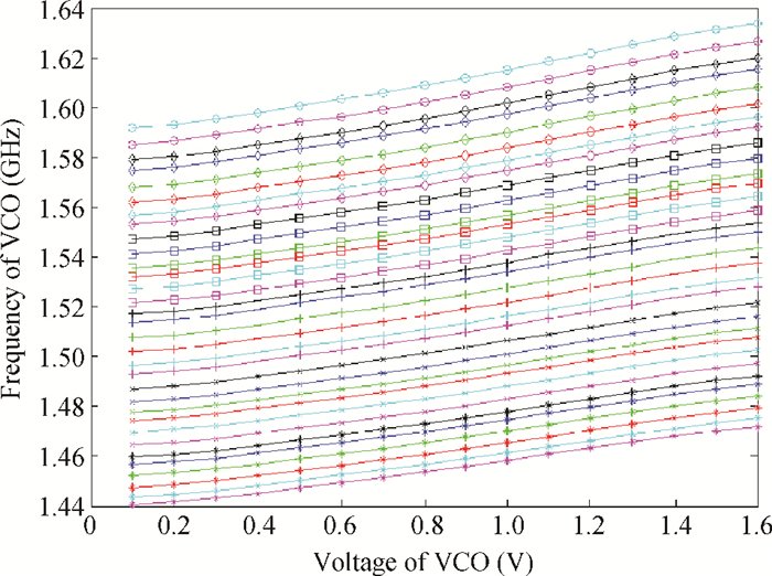
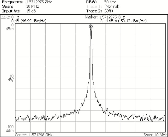
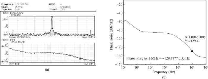
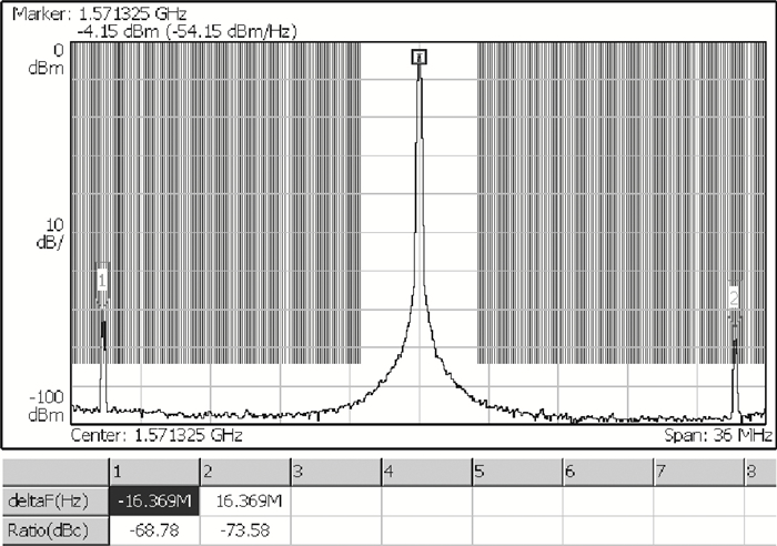
A low phase noise and low spur phase locked loop (PLL) frequency synthesizer for use in global navigation satellite system (GNSS) receivers is proposed. To get a low spur, the symmetrical structure of the phase frequency detector (PFD) produces four control signals, which can reach the charge pump (CP) simultaneously, and an improved CP is realized to minimize the charge sharing and the charge injection and make the current matched. Additionally, the delay is controllable owing to the programmable PFD, so the dead zone of the CP can be eliminated. The output frequency of the VCO can be adjusted continuously and precisely by using a programmable LC-TANK. The phase noise of the VCO is lowered by using appropriate MOS sizes. The proposed PLL frequency synthesizer is fabricated in a 0.18 μm mixed-signal CMOS process. The measured phase noise at 1 MHz offset from the center frequency is -127.65 dBc/Hz and the reference spur is -73.58 dBc.


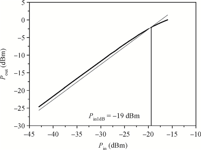
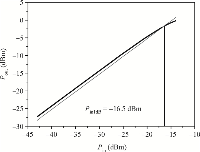
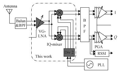
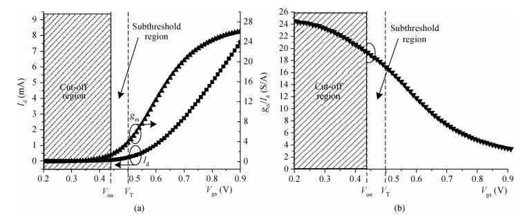
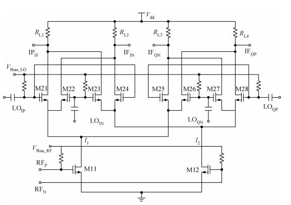
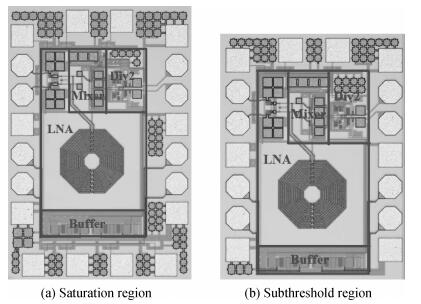
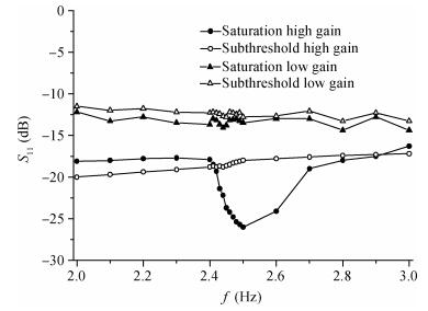
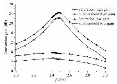
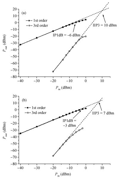
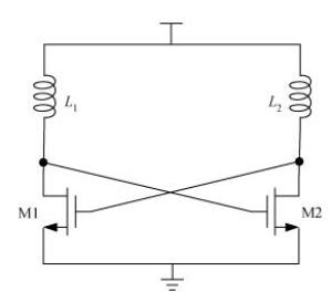
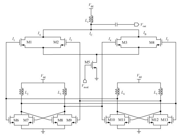
This paper presents the design of an ultralow power receiver front-end designed for a wireless sensor network (WSN) in a 0.18 μm CMOS process. The author designs two front-ends working in the saturation region and the subthreshold region respectively. The front-ends contain a two-stage cross-coupling cascaded common-gate (CG) LNA and a quadrature Gilbert IQ mixer. The measured conversion gain is variable with high gain at 24 dB and low gain at 7 dB for the saturation one, and high gain at 22 dB and low gain at 5 dB for the subthreshold one. The noise figure (NF) at high gain mode is 5.1 dB and 6.3 dB for each. The input 1 dB compression point (IP1dB) at low gain mode is about -6 dBm and -3 dBm for each. The front-ends consume about 2.1 mA current from 1.8 V power supply for the saturation one and 1.3 mA current for the subthreshold one. The measured results show that, comparing with the power consumption saving, it is worth making sacrifices on the performance for using the subthreshold technology.

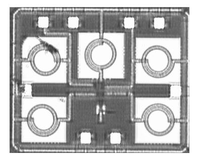
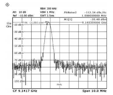
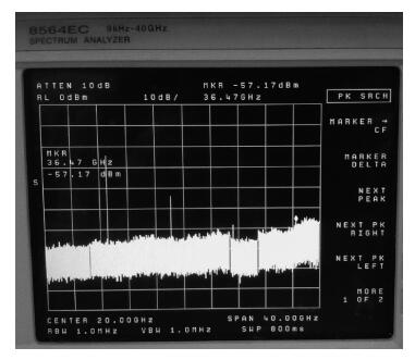
This paper presents a millimeter wave (mm-wave) oscillator that generates signal at 36.56 GHz. The mm-wave oscillator is realized in a UMC 0.18 μm CMOS process. The linear superposition (LS) technique breaks through the limit of cut-off frequency (fT), and realizes a much higher oscillation than fT. Measurement results show that the LS oscillator produces a calibrated -37.17 dBm output power when biased at 1.8 V; the output power of fundamental signal is -10.85 dBm after calibration. The measured phase noise at 1 MHz frequency offset is -112.54 dBc/Hz at the frequency of 9.14 GHz. This circuit can be properly applied to mm-wave communication systems with advantages of low cost and high integration density.


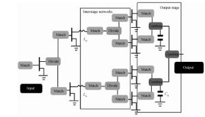
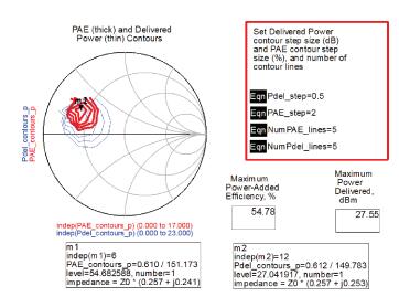
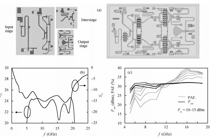
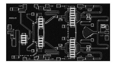
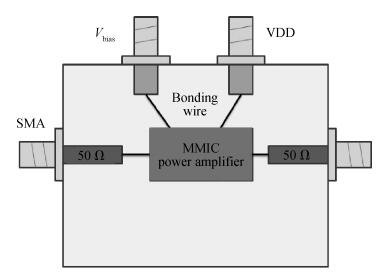
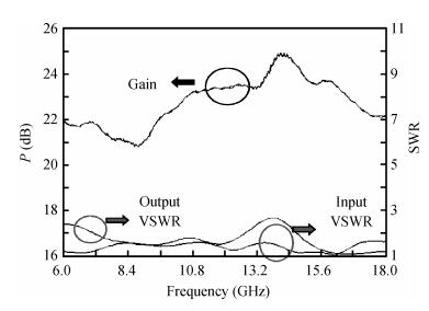
A three-stage monolithic microwave integrated circuit (MMIC) power amplifier from 6-18 GHz, which achieves high output power with excellent efficiency, is designed, fabricated and tested. Measured results show that the saturated output power and the small signal gain are about 32 dBm and 23 dB, respectively. Thus, the power added efficiency of about 28% indicates that it is useful in various communication systems.


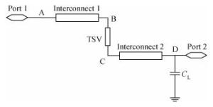
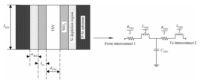
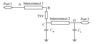
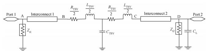
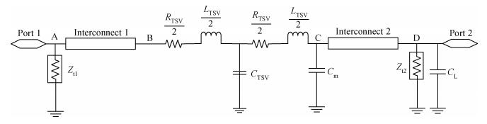
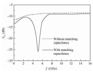
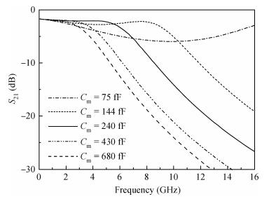
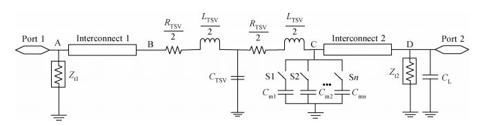
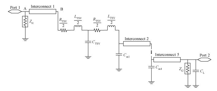
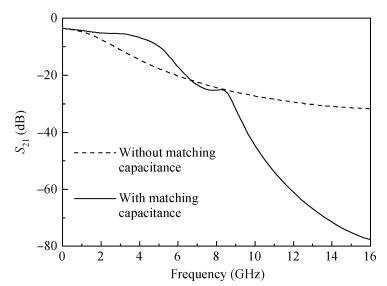
In high speed three-dimensional integrated circuits (3D ICs), through silicon via (TSV) insertion causes impedance discontinuities along the interconnect-TSV channel that results in signal reflection. As demonstrated for a two-plane interconnect structure connected by a TSV, we incorporate an appropriate capacitance at the junction to mitigate the signal reflection with gigascale frequencies. Based on 65 nm technology and S-parameter analysis, the decrease of signal reflection can be 189% at the tuned frequency of 5 GHz. Extending this method to the five-plane interconnect structure further, the reduction of signal reflection can achieve 400%. So we could broaden this method to any multilevel 3D interconnect structures. This method can also be applied to a circuit with tunable operating frequencies by digitally connecting the corresponding matching capacitance into the circuit through switches. There are remarkable improvements of the quality of the transmitting signals.


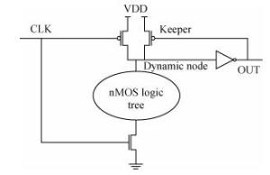
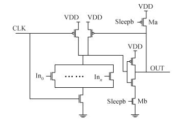
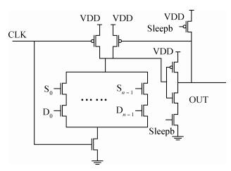
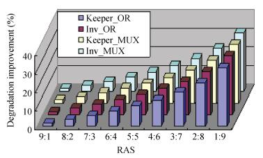
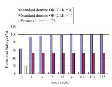
NBTI-induced transistor aging has become a prominent factor affecting the reliability of circuits. Reducing leakage consumption is one of the major design goals. Domino logic circuits are applied extensively in high-performance integrated circuits. A circuit technique for mitigating NBTI-induced degradation and reduce standby leakage current is presented in this paper. Two transistors are added to the standard domino circuit to pull both the dynamic node and the output up to VDD, which puts both the keeper and the inverter pMOS transistor into recovery mode in standby mode. Due to the stack effect, leakage current is reduced by the all-0 input vector and the added transistors. Experimental results reveal up to 33% NBTI-induced degradation reduction and up to 79% leakage current reduction.


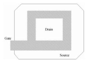
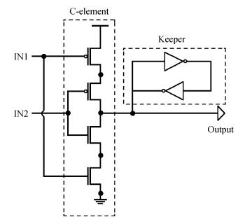
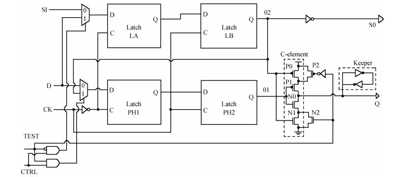
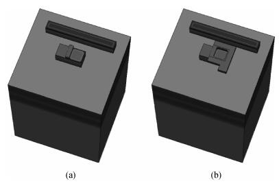
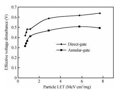
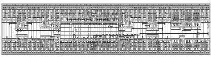
This paper presents a radiation hardened flip-flop with an annular gate and a Muller C-element. The proposed cell has multiple working modes which can be used in different situations. Each part of the cell can be verified easily and completely by using different modes. This cell has been designed under an SMIC 0.13 μm process and 3-D simulated by using Synopsys TCAD. Heavy-ion testing has been done on the cell and its counterparts. The test results demonstrate that the presented cell reduces the cell's saturation cross section by approximately two orders of magnitude with little penalty on performance.

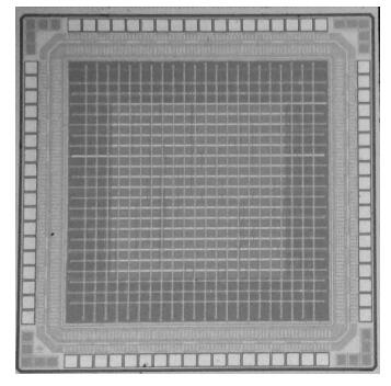
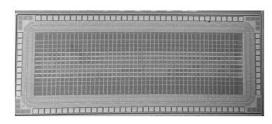

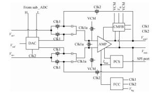
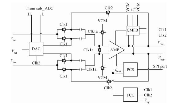
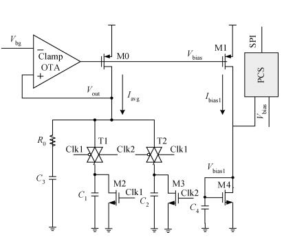
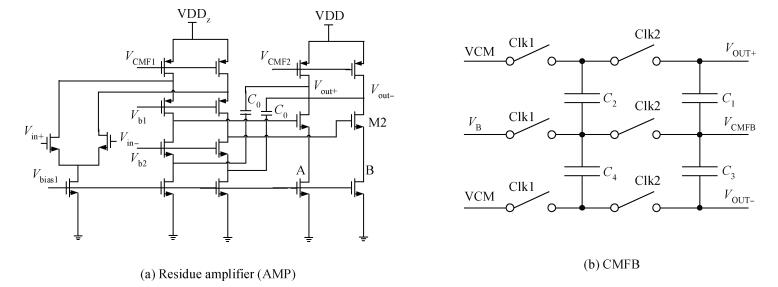
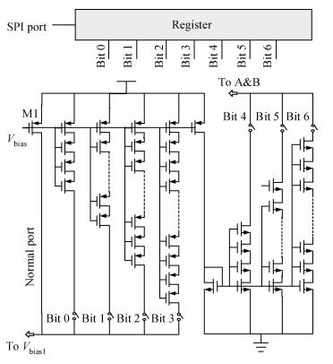
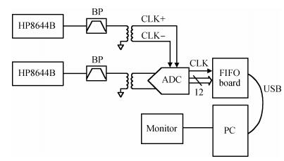
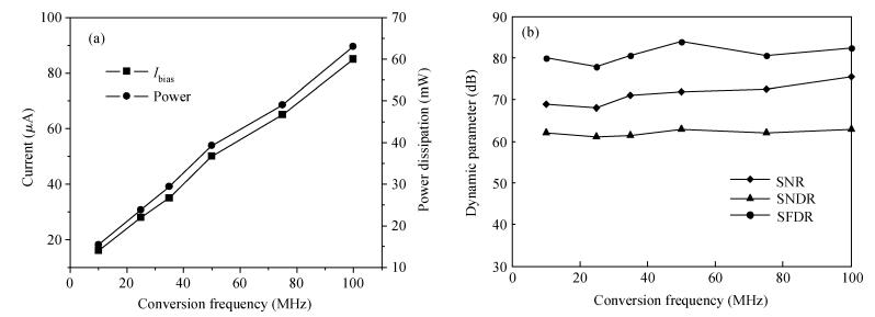
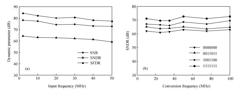
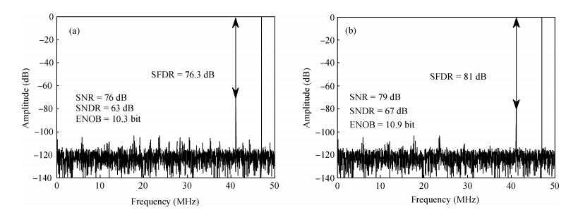
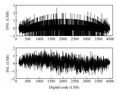
A programmable high precision multiplying DAC (MDAC) is proposed. The MDAC incorporates a frequency-current converter (FCC) to adjust the power versus sampling rate and a programmable operational amplifier (POTA) to achieve the tradeoff between resolution and power of the MDAC, which makes the MDAC suitable for a 12 bit SHA-less pipelined ADC. The prototype of the proposed pipelined ADC is implemented in an SMIC CMOS 0.18 μm 1P6M process. Experimental results demonstrate that power of the proposed ADC varies from 15.4 mW (10 MHz) to 63 mW (100 MHz) while maintaining an SNDR of 60.5 to 63 dB at all sampling rates. The differential nonlinearity and integral nonlinearity without any calibration are no more than 2.2/-1 LSB and 1.6/-1.9 LSB, respectively.


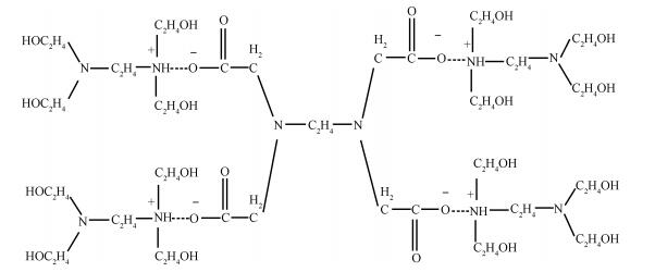
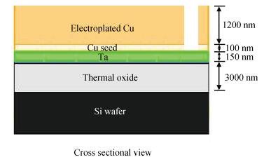
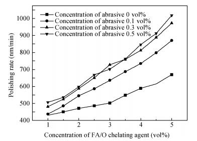
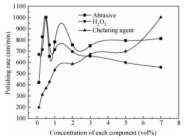
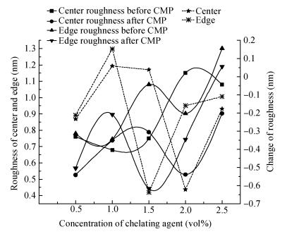
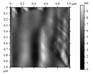
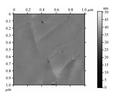
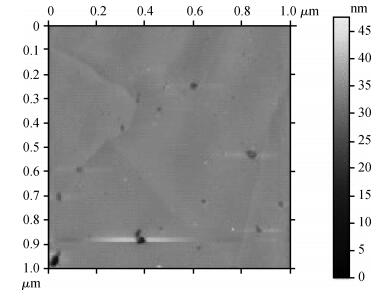
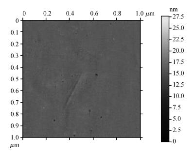
The mechanism of the FA/O chelating agent in the process of chemical mechanical polishing (CMP) is introduced. CMP is carried on a Φ300 mm copper film. The higher polishing rate and lower surface roughness are acquired due to the action of an FA/O chelating agent with an extremely strong chelating ability under the condition of low pressure and low abrasive concentration during the CMP process. According to the results of several kinds of additive interaction curves when the pressure is 13.78 kPa, flow rate is 150 mL/min, and the rotating speed is 55/60 rpm, it can be demonstrated that the FA/O chelating agent plays important role during the CMP process.