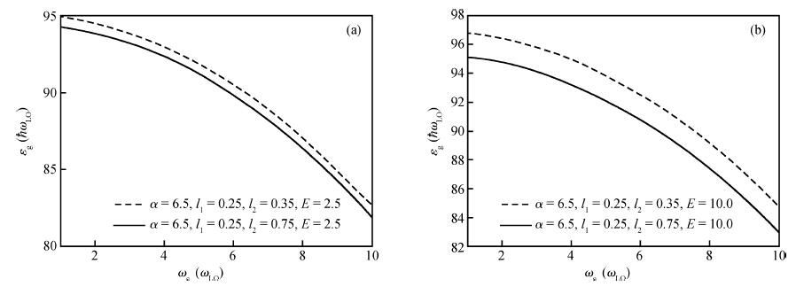
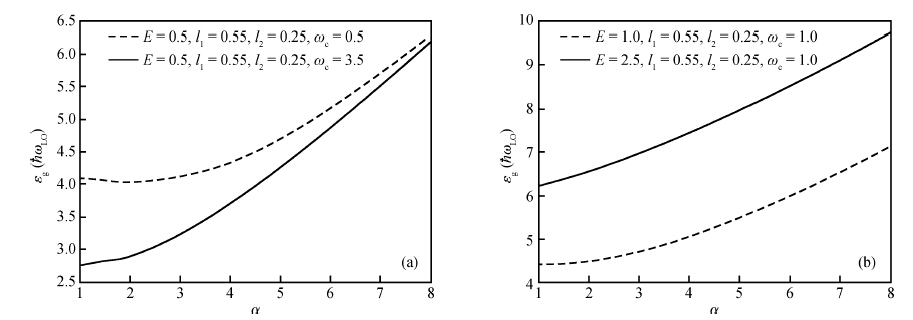
We investigated the influence of electric field and magnetic field on the ground state energy of polaron in spherical semiconductor quantum dot (QD) using a modified Lee Low Pines (LLP) method. The numerical results show the increase of the ground state energy with the increase of the electric field and the decreasing with the magnetic field. The modulation of the electric field, magnetic field and the confinement lengths lead to the control of the decoherence of the system.
Issue Browser
Volume 36, Issue 7,
Jul 2015

J. Semicond.
2015, 36(7): 072002 doi: 10.1088/1674-4926/36/7/072002

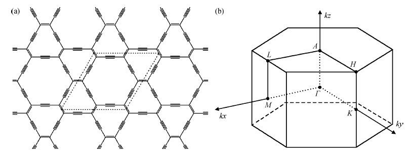
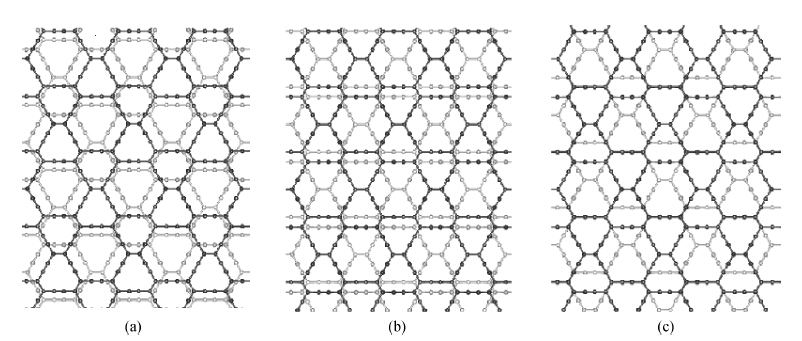
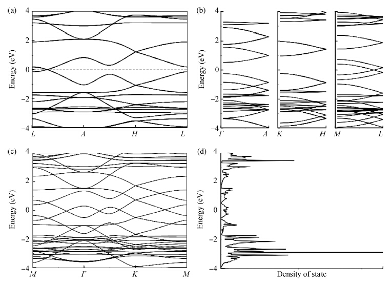
β-graphyne, a carbon allotrope, is a gapless semiconductor with hexagonal lattice symmetry, just like graphene. We calculated the optimized structure and electronic structures of some possible three-dimensional β-graphyne stacking arrangements by means of the first-principles frozen-core projector augmented-wave method implemented in the Vienna ab initio simulation package. The optimized lattice constant a of the three-dimensional β-graphyne turns out to be 9.46 Å, which is slightly smaller than its two-dimensional counterpart. The binding energy is about 90% of that of graphite, which suggests that three-dimensional β-graphyne will be stable when it is synthesized. The band structure is calculated via the hybrid functional. We found that the most stable three-dimensional stacking arrangement is an indirect band gap semiconductor with an energy gap of 0.1 eV.
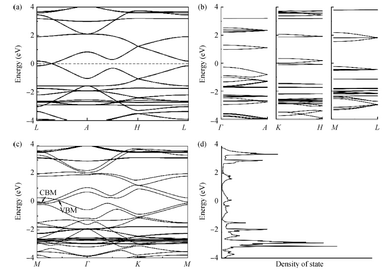
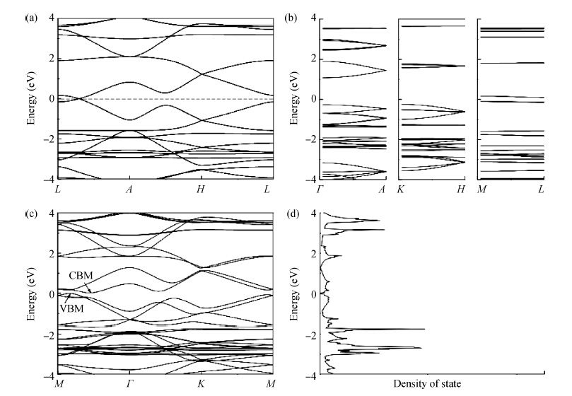
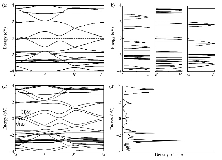
J. Semicond.
2015, 36(7): 072003 doi: 10.1088/1674-4926/36/7/072003

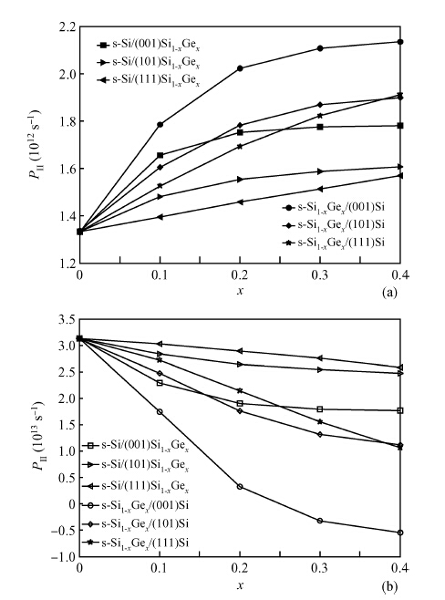
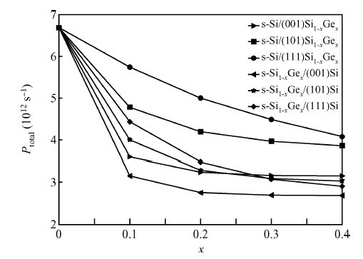
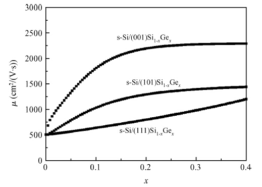
Based on Fermi's golden rule and the theory of Boltzmann collision term approximation, the hole scattering mechanism related to stress and orientation in Si-based strained materials was studied in-depth. The results show that: (1) the total hole scattering rates in Si-based strained materials decrease obviously under strain; (2) the turn is Si/(111)Si1-xGex > Si/(101)Si1-xGex > Si1-xGex/(111)Si > Si1-xGex/(101)Si > Si/(001)Si1-xGex > Si1-xGex/(001)Si when Ge fraction is about 0.2; (3) the decreasing total hole scattering rates of in strained materials with the increasing stress is mainly caused the decreasing acoustic phonon scattering rate under strain. The theoretical conclusions obtained could provide important references for researching the hole mobility and the understanding of Si-based materials or other physical strained materials.


J. Semicond.
2015, 36(7): 073001 doi: 10.1088/1674-4926/36/7/073001

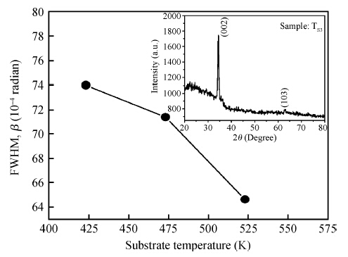
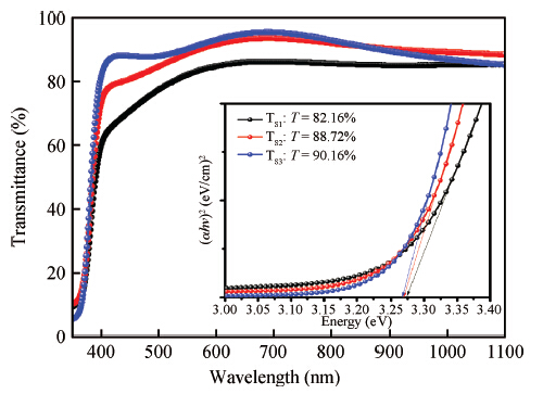
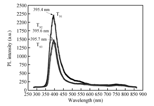
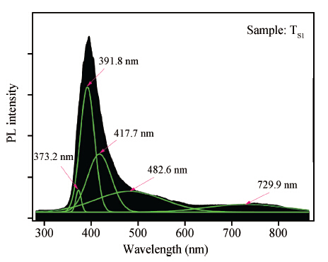
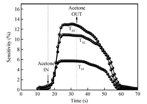
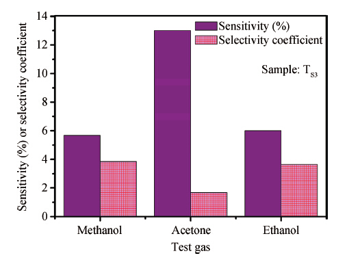
Zinc oxide (ZnO) thin films were prepared onto glass substrates at moderately low growth temperature by two-stage spray pyrolysis technique. The effects of growth temperature on structural, optical and acetone detection properties were investigated with X-ray diffractometry, a UV-visible spectrophotometer, photoluminescence (PL) spectroscopy and a homemade gas sensor testing unit, respectively. All the films are polycrystalline with a hexagonal wurtzite phase and exhibit a preferential orientation along [002] direction. The film crystallinity is gradually enhanced with an increase in growth temperature. The optical measurements show that all the films are physically highly transparent with a transmittance greater than 82% in the visible range. The band gap of the film is observed to exhibit a slight red shift with an increasing growth temperature. The PL studies on the films show UV/violet PL band at ~ 395 nm. Among all the films investigated, the film deposited at 250 ℃ demonstrates a maximum sensitivity of 13% towards 20 ppm of acetone vapors at 300 ℃ operating temperature.

J. Semicond.
2015, 36(7): 073002 doi: 10.1088/1674-4926/36/7/073002

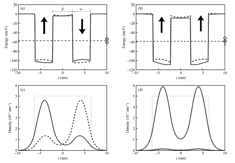
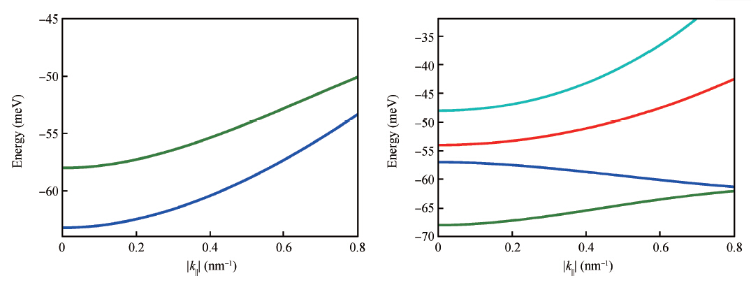
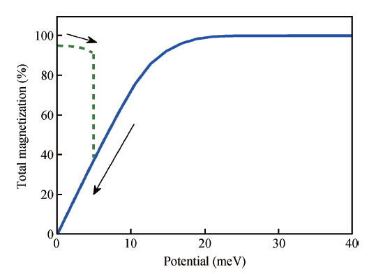
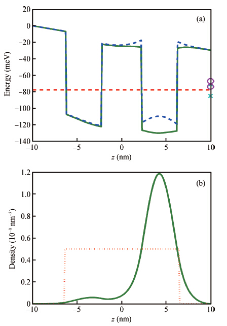
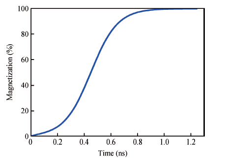
The interplay between the electric and magnetic properties in a double quantum well heterostructure doped by magnetic ions is theoretically investigated. In this material, the magnetism is mediated by the hole gas. The total magnetic polarization of the system is controllable by an external applied bias. The device has two equilibrium states (symmetric and antisymmetric configurations). In the stable configuration (anti-ferromagnetic type), the particle spin distribution is reversed in the adjacent wells. The stability of the system is investigated by simulating the interaction of the hole gas with the light. By using an ab initio method, we estimate the switching time of the device.
J. Semicond.
2015, 36(7): 073003 doi: 10.1088/1674-4926/36/7/073003

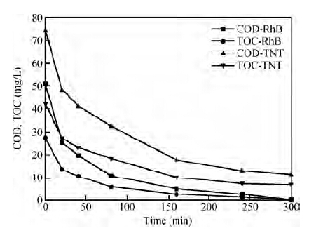
Cu2ZnSnS4 (CZTS) is a main candidate material for solar energy conversion through both photovoltaics and photocatalysis based on environmentally friendly elements and with a direct band gap of 1.5 eV. We report the synthesis of quasi Cu2ZnSnS4 microparticles with unprecedented narrow size distributions. The structural, morphological and core level analysis has been carried out by XRD, SEM and XPS techniques. These microparticles have shown excellent photocatalytic activity toward degradation of Rhodamine B dye (RhB) and TNT under visible light. The extent of mineralization has been analyzed by COD and TOC values. Photocatalytic water splitting for H2 generation has also been reported.


J. Semicond.
2015, 36(7): 073004 doi: 10.1088/1674-4926/36/7/073004

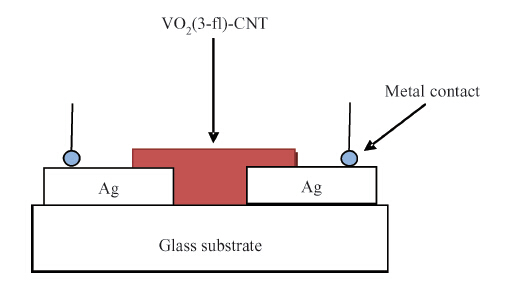
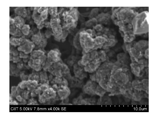
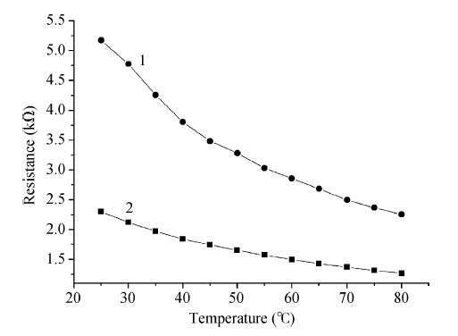
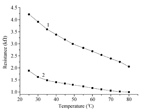
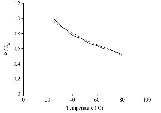
A vanadium complex (VO2(3-fl)) and CNT composite film based temperature sensor is reported in this study. Surface-type silver electrodes were deposited on the glass substrates. A thin film of VO2(3-fl) and CNT composite was coated as a temperature-sensing material on the top of the pre-patterned Ag electrodes. The temperature-sensing principle of the sensor was based on the conductivity change of the coated sensing element upon heating or cooling processes. DC and AC (100 Hz) resistances of the temperature sensor decreased quasi-linearly with increasing the temperature in the range of 25-80 ℃. The overall resistance of the sensor decreases by 1.8-2.1 and 1.9-2.0 times at DC and AC voltage, respectively. The resistance temperature coefficients of the sensor were in the range of -(0.9-1.3)% and -(1.1-1.3)% at DC and AC voltage, respectively. The properties of the sensor studied in this work, make it beneficial to be used in the instruments for environmental monitoring of temperature.

J. Semicond.
2015, 36(7): 073005 doi: 10.1088/1674-4926/36/7/073005

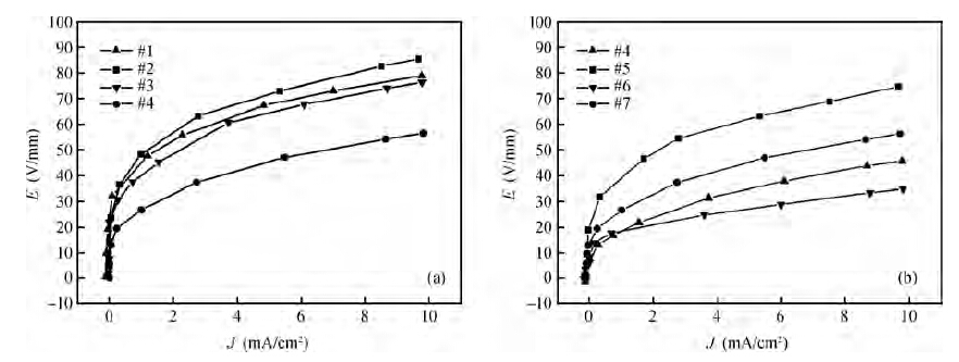
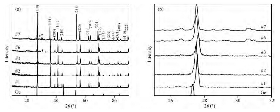
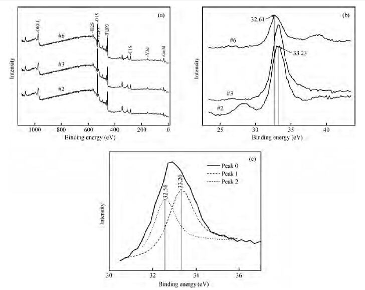
An investigation was made into the effect of doping with the elemental crystal Ge or/and GeO2 on the TiO2-V2O5-Y2O3 varistor ceramics. The result shows that as the doping contents of V2O5 and Y2O3 are 0.5 mol%, respectively, co-doping with 0.3 mol% Ge and 0.9 mol% GeO2 makes the highest α value (α = 12.8), the lowest breakdown voltage V1mA (V1mA = 15.8 V/mm) and the highest grain boundary barrier ΦB (ΦB = 1.48 eV), which is remarkably superior to the TiO2-V2O5-Y2O3 varistor ceramics undoped with Ge and GeO2 and mono-doped with Ge or GeO2. The TiO2-V2O5-Y2O3-Ge-GeO2 ceramic has the prospect of becoming a novel varistor ceramic with excellent electrical properties.


J. Semicond.
2015, 36(7): 073006 doi: 10.1088/1674-4926/36/7/073006

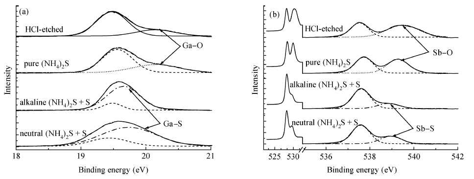
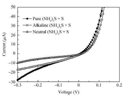
The surface chemical properties of gallium antimonide (GaSb) after ammonium sulfide ((NH4)2S) solution passivation have been studied by X-ray photoelectron spectroscopy (XPS), time of flight secondary ion mass spectroscopy (TOF-SIMS) and I-V measurement. An advantage of neutral (NH4)2S + S solution over pure (NH4)2S solution and alkaline (NH4)2S + S solution has been found in the ability to passivate the GaSb surface by contrast and comparison. It has been found that alkaline (NH4)2S + S solution passivation effectively removes oxides of the GaSb surface and forms sulfide products to improve device performance. TOF-SIMS complementally demonstrates that pure (NH4)2S passivation did form sulfide products, which are too soluble to really exist. The lowest roughness determined using a 3D optical profilometer and the highest improved SBD quality proved that neutral (NH4)2S + S solution passivation worked much better in improving the surface properties of GaSb.


J. Semicond.
2015, 36(7): 074001 doi: 10.1088/1674-4926/36/7/074001

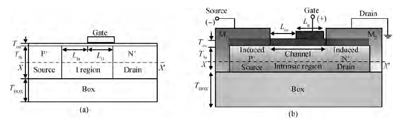
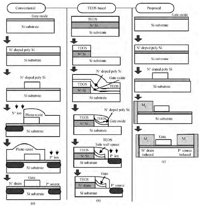
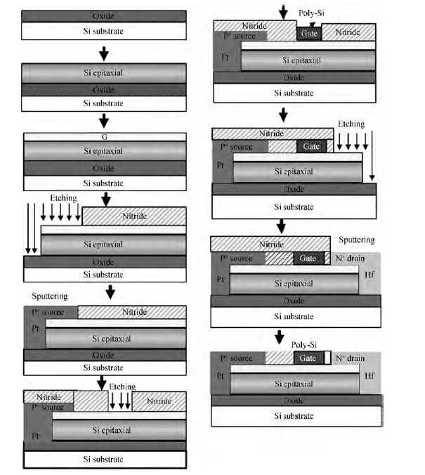
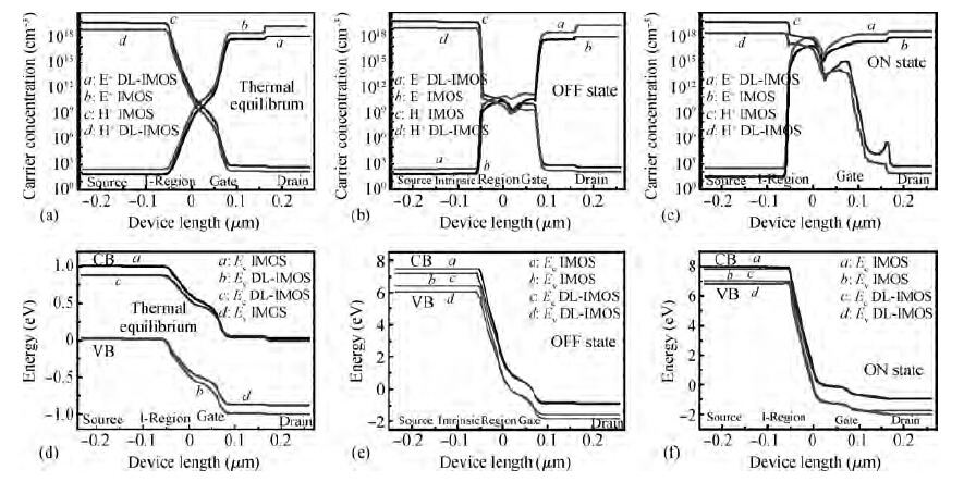
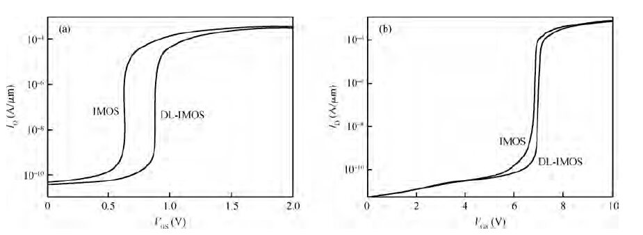
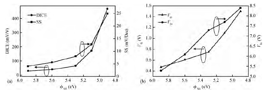
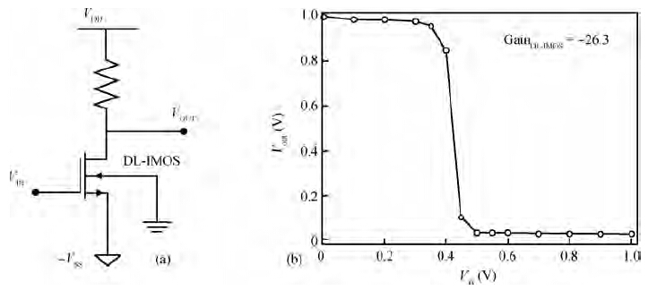
We propose a unique approach for realizing dopingless impact ionization MOS (DL-IMOS) based on the charge plasma concept as a remedy for complex process flow. It uses work-function engineering of electrodes to form charge plasma as surrogate doping. This charge plasma induces a uniform p-region in the source side and an n-region in the drain side on intrinsic silicon film with a thickness less than the intrinsic Debye length. DL-IMOS offers a simple fabrication process flow as it avoids the need of ion implantation, photo masking and complicated thermal budget via annealing devices. The lower thermal budget is required for DL-IMOS fabrication enables its fabrication on single crystal silicon-on-glass substrate realized by wafer scale epitaxial transfer. It is highly immune to process variations, doping control issues and random dopant fluctuations, while retaining the inherent advantages of conventional IMOS. To epitomize the fabrication process flow for the proposed device a virtual fabrication flow is also proposed here. Extensive device simulation of the major device performance metrics such as subthreshold slope, threshold voltage, drain induced current enhancement, and breakdown voltage have been done for a wide range of electrodes work-function. To evaluate the potential applications of the proposed device at circuit level, its mixed mode simulations are also carried out.


J. Semicond.
2015, 36(7): 074002 doi: 10.1088/1674-4926/36/7/074002

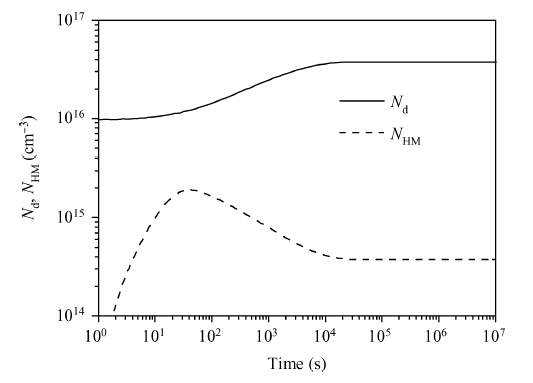
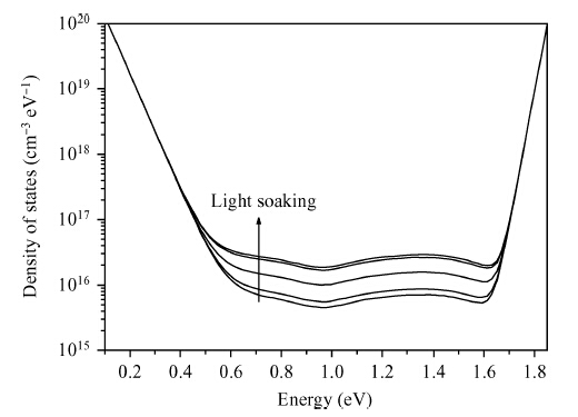
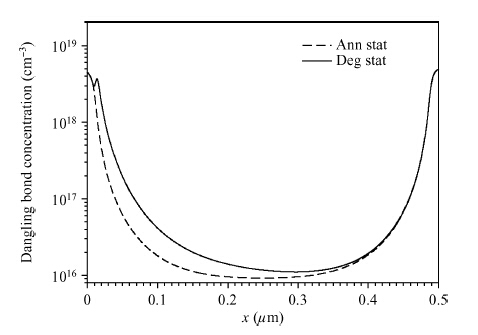
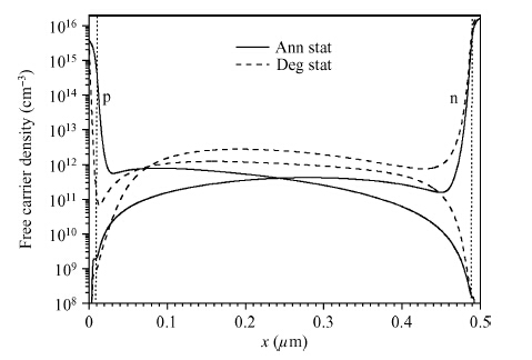
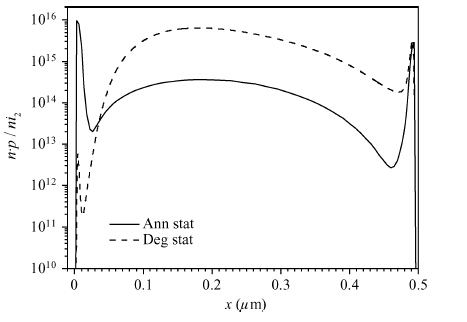
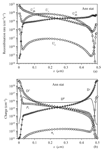
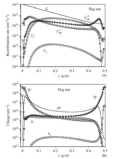
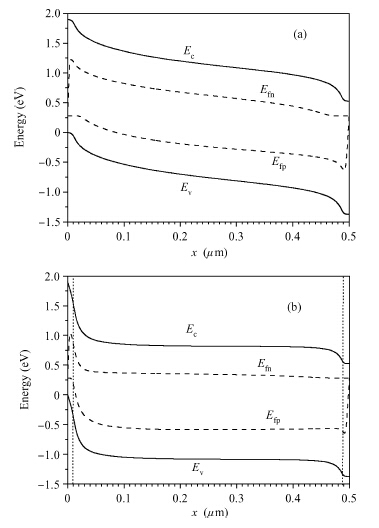
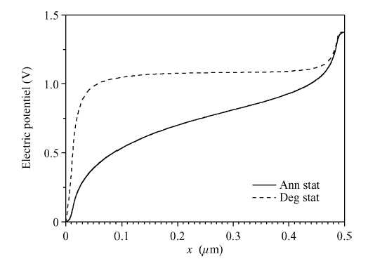
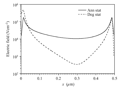
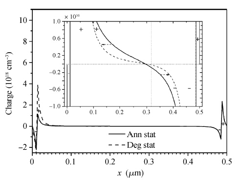
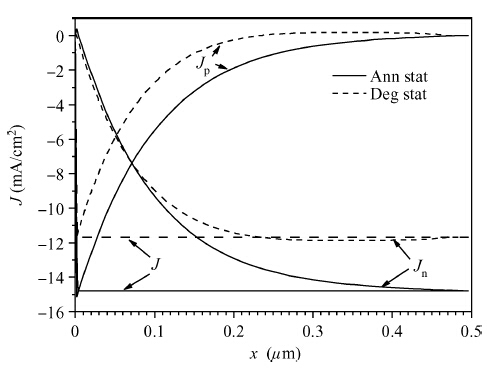
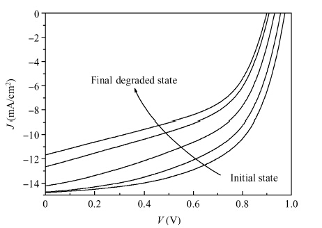
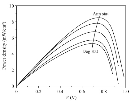
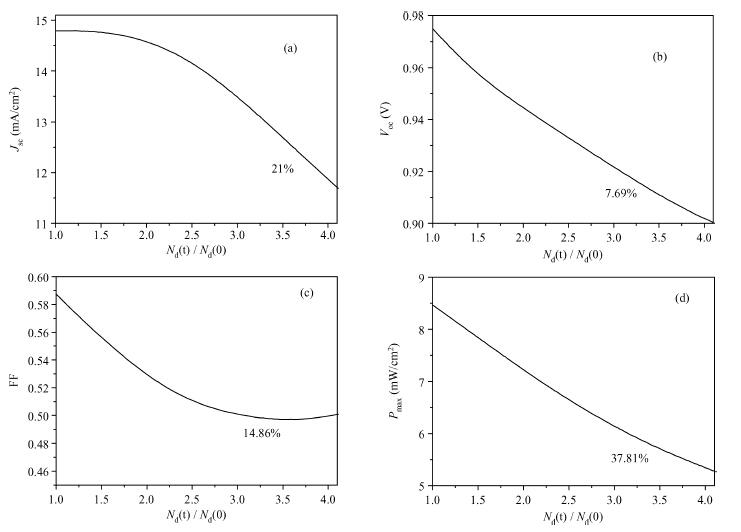
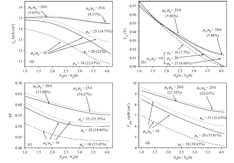
Using a previous model, which was developed to describe the light-induced creation of the defect density in the a-Si:H gap states, we present in this work a computer simulation of the a-Si:H p-i-n solar cell behavior under continuous illumination. We have considered the simple case of a monochromatic light beam nonuniformly absorbed. As a consequence of this light-absorption profile, the increase of the dangling bond density is assumed to be inhomogeneous over the intrinsic layer (i-layer). We investigate the internal variable profiles during illumination to understand in more detail the changes resulting from the light-induced degradation effect. Changes in the cell external parameters including the open circuit voltage, Voc, the short circuit current density, Jsc, the fill factor, FF, and the maximum power density, Pmax, are also presented. This shows, in addition, the free carrier mobility influence. The obtained results show that Voc seems to be the less affected parameter by the light-induced increase of the dangling bond density. Moreover, its degradation is very weak-sensitive to the free carrier mobility. Finally, the free hole mobility effect is found to be more important than that of electrons in the improvement of the solar cell performance.


J. Semicond.
2015, 36(7): 074003 doi: 10.1088/1674-4926/36/7/074003

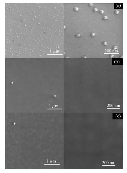
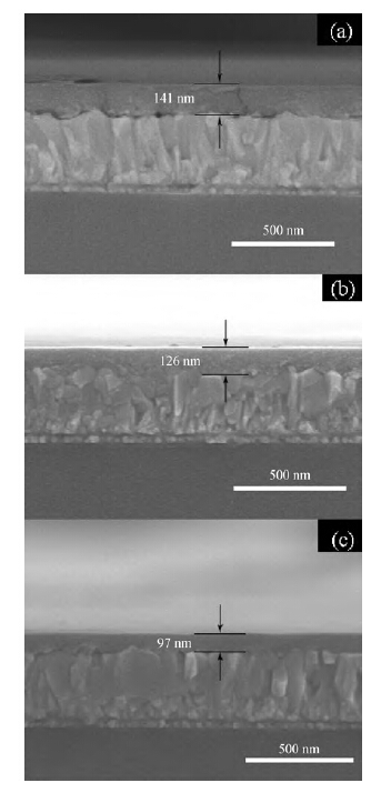
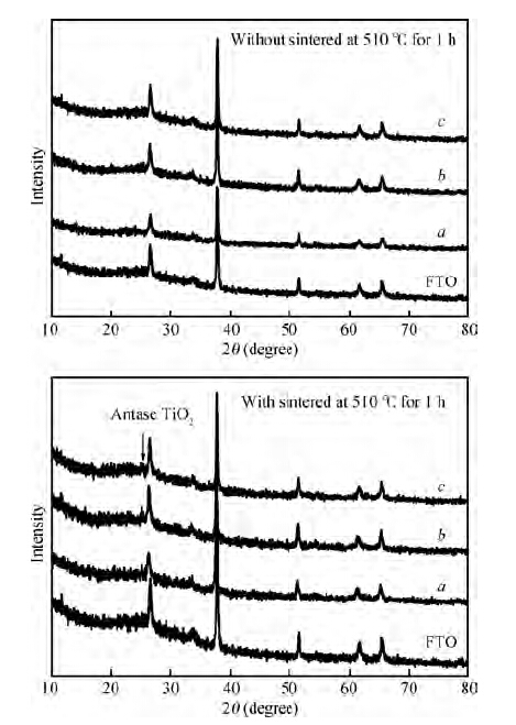
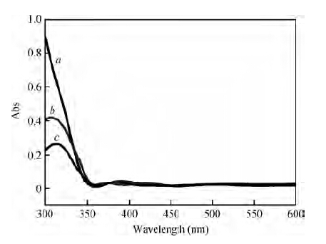
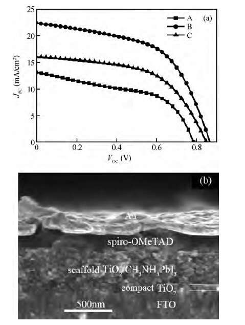
A hydrolysis process was applied to prepare the compact TiO2 layer using the fresh metastable TiCl4 isopropanol/water solution as the precursor solution for the preparation of the inorganic-organic hybrid heterojunction perovskite solar cells. The optimal compact TiO2 layer prepared from the aqueous solution of 2 mol· L-1 TiCl4 diluted in isopropanol at 1 : 3 by volume as precursor solution was uniform and with a film thickness of 126 nm. The corresponding perovskite solar cell gave a photovoltaic conversion efficiency of 10.61%.

J. Semicond.
2015, 36(7): 074004 doi: 10.1088/1674-4926/36/7/074004

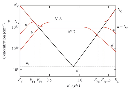
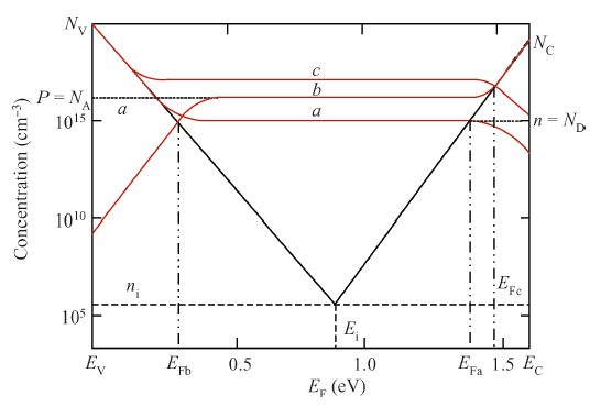
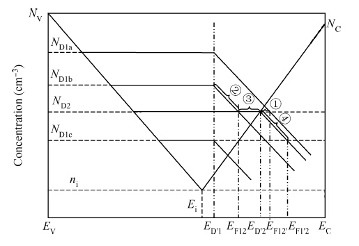
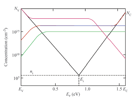
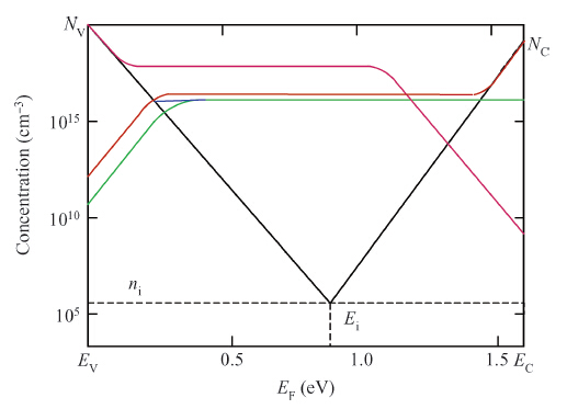
In thin film solar cells, the semiconductor materials usually contain multiple impurity/defect states as donor or acceptor dopants. The local charge neutrality (LCN) condition determines the equilibrium Fermi (EF) level and concentration of electrons and holes. However, the equation of LCN is a transcendental equation of EF. It is impossible to find its analytical solution and we can only solve it by graphic or numerical method. A simple approximate graphic method (GM) used for estimation of majority carrier compensation of semiconductors with multiple donors and acceptors was proposed by Chin. By introducing the concept of ranking the dopants and the wrapping step function, dopants concentration and Fermi level could be obtained easily. In this paper, we analyze the graphic method and propose a new numeric graphic method (NGM) based on GM. In addition, comparison of NGM with NM and analytics of the accuracy of GM are presented. With numerical calculation, some procedures of GM extending the application of GM are improved.

J. Semicond.
2015, 36(7): 074005 doi: 10.1088/1674-4926/36/7/074005

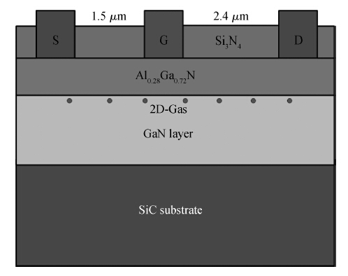
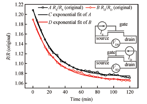
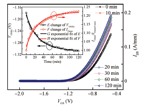
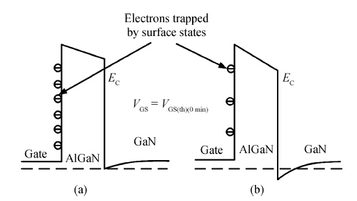
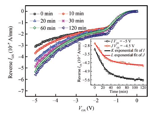
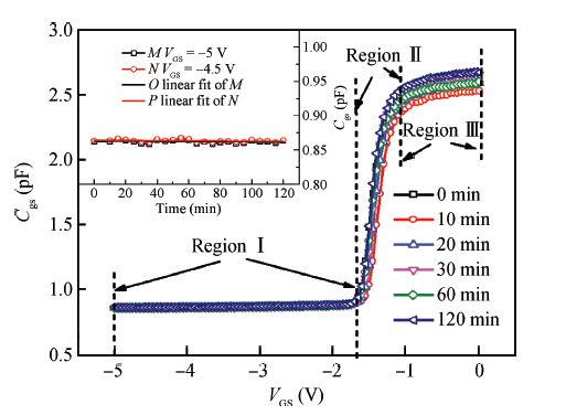
The phenomenon of self-changing on the device parameters and characteristics after a step voltage stress was applied to the gate is studied in AlGaN/GaN high electron mobility transistors. The device was measured every 5 min after the stress was removed. The large-signal parasitic source (drain) resistance, transfer characteristics, threshold voltage, drain-source current, gate-source (drain) reverse current-voltage characteristics changed spontaneously after the removal of the stress. The time constant of the self-changing was about 25-27 min. The gate-source (drain) capacitance-voltage characteristics were constant during this process. Electrons were trapped by the surface states and traps in the AlGaN barrier layer when the device was under stress. The traps in the AlGaN barrier layer then released electrons in less than 10 s. The surface states released electrons continuously during the entire measurement stage, leading to the self-changing of mearsurement result.

J. Semicond.
2015, 36(7): 074006 doi: 10.1088/1674-4926/36/7/074006

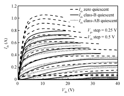
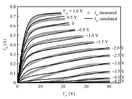
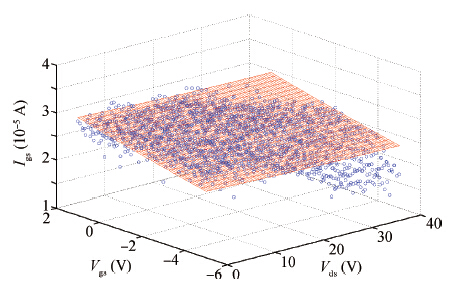
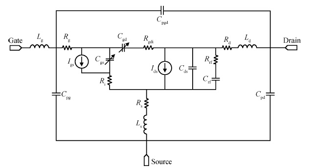
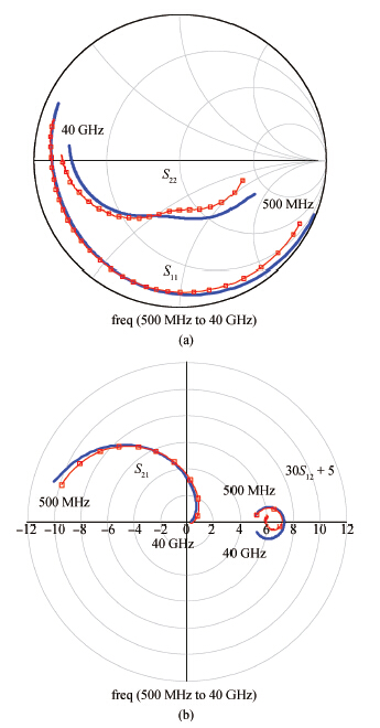
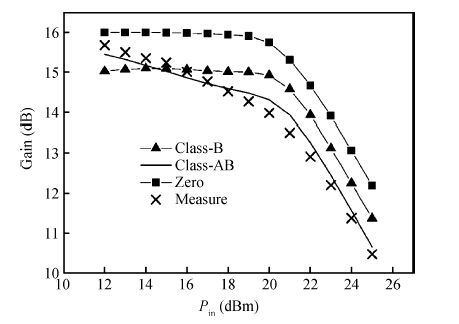
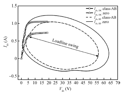
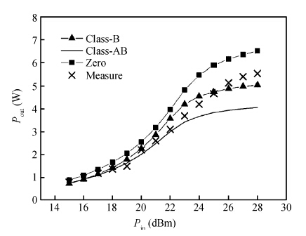
An optimized modeling method of 8 × 100 μm AlGaN/GaN-based high electron mobility transistor (HEMT) for accurate continuous wave (CW) and pulsed power simulations is proposed. Since the self-heating effect can occur during the continuous operation, the power gain from the continuous operation significantly decreases when compared to a pulsed power operation. This paper extracts power performances of different device models from different quiescent biases of pulsed current-voltage (I-V) measurements and compared them in order to determine the most suitable device model for CW and pulse RF microwave power amplifier design. The simulated output power and gain results of the models at Vgs = -3.5 V, Vds = 30 V with a frequency of 9.6 GHz are presented.


J. Semicond.
2015, 36(7): 074007 doi: 10.1088/1674-4926/36/7/074007

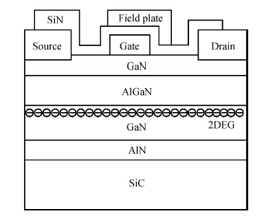
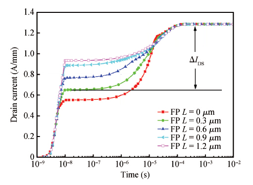
The relationship between AlGaN/GaN HEMT gate field plate (FP) and surface-state-related gate lag phenomena is investigated by two-dimensional numerical transient simulations to study the mechanism of the influence of FPs on current collapse. The simulations reveal that adding a field plate has a noticeable impact on the extent of current collapse while it has no influence on lapsed time. The FP is found to suppress current collapse through reducing the ionization probability of surface states by enhancing free hole accumulation next to the AlGaN surface between gate and drain.


J. Semicond.
2015, 36(7): 074008 doi: 10.1088/1674-4926/36/7/074008

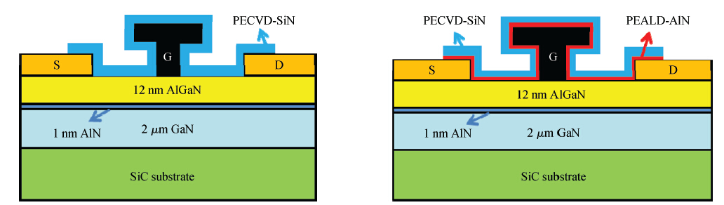
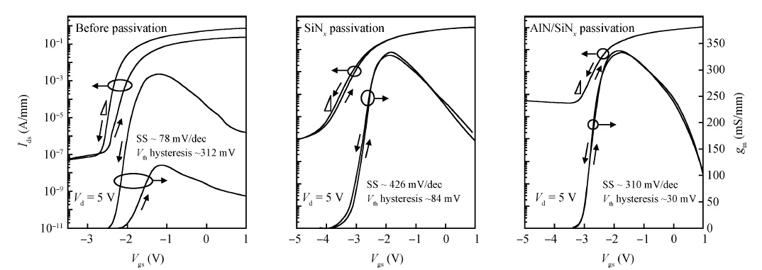
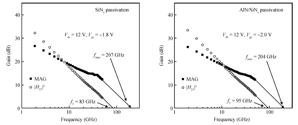
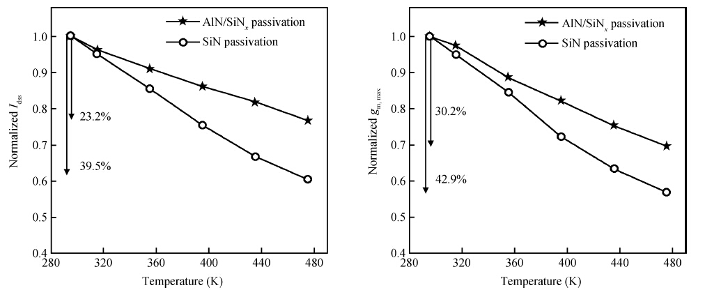
AlGaN/GaN high electron-mobility transistors (HEMTs) with 5 nm AlN passivation by plasma enhanced atomic layer deposition (PEALD) were fabricated, covered by 50 nm SiNx which was grown by plasma enhanced chemical vapor deposition (PECVD). With PEALD AlN passivation, current collapse was suppressed more effectively and the devices show better subthreshold characteristics. Moreover, the insertion of AlN increased the RF transconductance, which lead to a higher cut-off frequency. Temperature dependence of DC characteristics demonstrated that the degradations of drain current and maximum transconductance at elevated temperatures for the AlN/SiNx passivated devices were much smaller compared with the devices with SiNx passivation, indicating that PEALD AlN passivation can improve the high temperature operation of the AlGaN/GaN HEMTs.
J. Semicond.
2015, 36(7): 074009 doi: 10.1088/1674-4926/36/7/074009

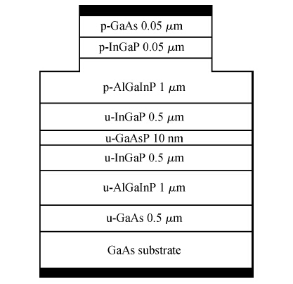
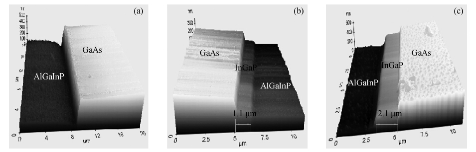
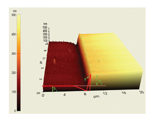
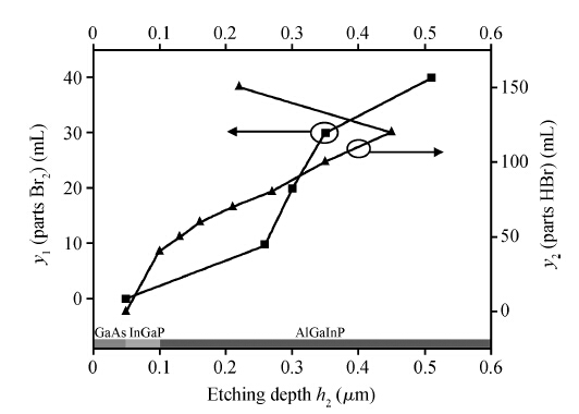
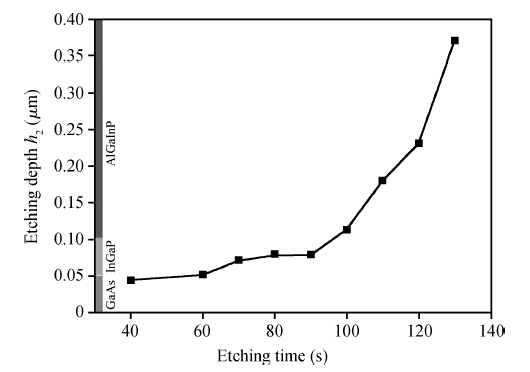
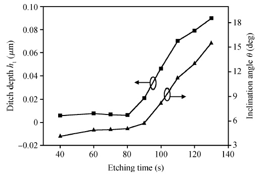
The fabrication of ridge waveguide of 808 nm GaAs-based laser diodes by wet chemical etching is investigated. The etching behavior of GaAs, InGaP and AlGaInP in various solutions is evaluated. As a result, the etching solutions simultaneously corroding InGaP and AlGaInP layers are searched successfully. Effects of etching time and the concentration of mixtures on etching depth and the geometrical shape of ridge are analyzed. It is found that under proper conditions, appropriate etching depth and smooth surfaces can be obtained and the steep degree of pattern can be accepted, especially for wide ridge waveguide laser diodes.
J. Semicond.
2015, 36(7): 074010 doi: 10.1088/1674-4926/36/7/074010

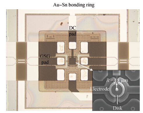
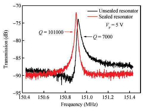
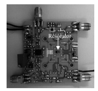
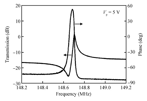
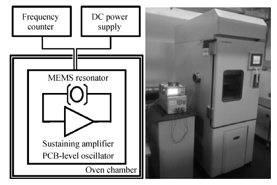
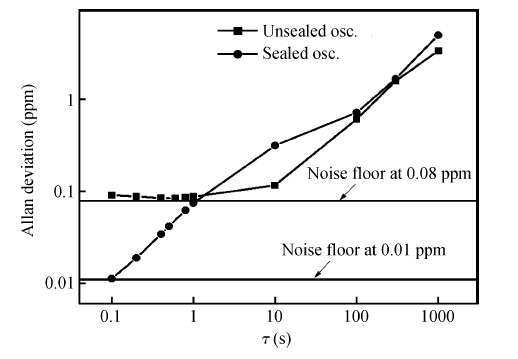
This paper presents a high-Q RF MEMS oscillator consisting of a micro-disk resonator and low noise feedback circuits. The oscillator has high frequency stability and low phase noise. The two-port resonator was hermetically encapsulated using low-cost Sn-rich Au-Sn solder bonding, which significantly improves the frequency stability. A low noise oscillator circuit was designed with a two-stage amplifying architecture which effectively improves both the frequency stability and phase noise performance. The measured phase noise is -96 dBc/Hz at 1 kHz offset and -128 dBc/Hz at far-from-carrier offsets. Moreover, the medium-term frequency stability and Allan deviation of the oscillator are ± 4 ppm and 10 ppb, respectively. The oscillator is a promising component in future wireless communication application.


J. Semicond.
2015, 36(7): 075001 doi: 10.1088/1674-4926/36/7/075001

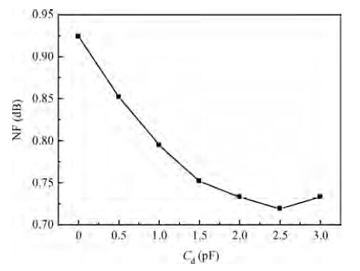
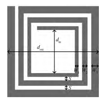
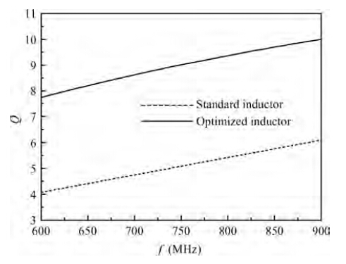
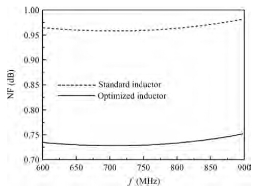
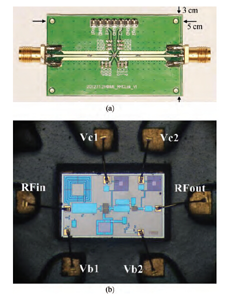
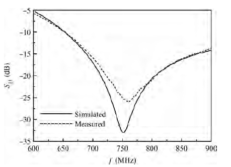
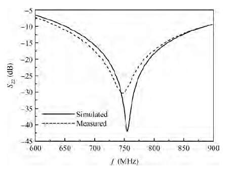
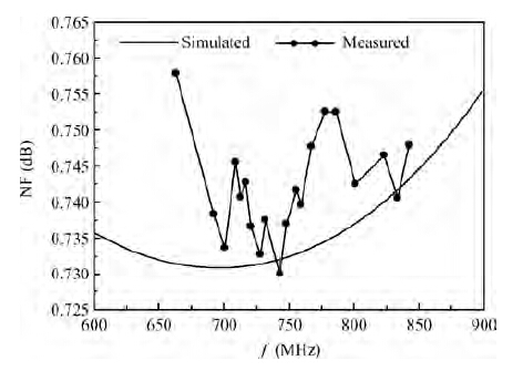
A two-stage monolithic microwave integrated circuit (MMIC) low noise amplifier (LNA) fabricated in 0.5 μm GaAs pHEMT is presented. The Miller effect introduced by the parasitic gate-drain capacitance is utilized to decrease the value of the input inductor. Additionally, the input on-chip inductor is a novel high Q gradual structure. The noise figure is reduced with these two methods. With good input and output matching, the LNA achieves a noise figure of 0.75 dB and a small signal gain of 32.7 dB over 698-806 MHz. The input 1 dB compression point is -21.8 dBm and the input third order interception point is -10 dBm.


J. Semicond.
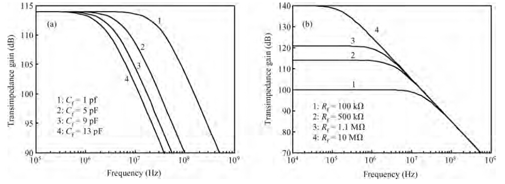
2015, 36(7): 075002 doi: 10.1088/1674-4926/36/7/075002

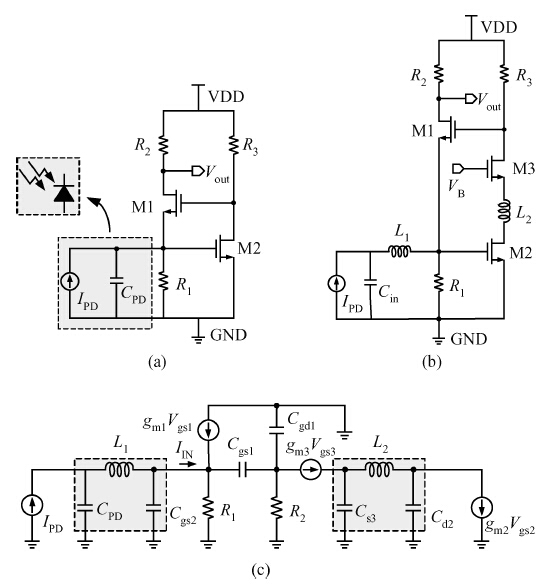
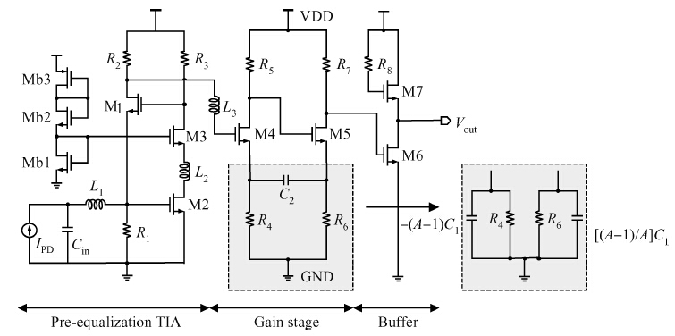
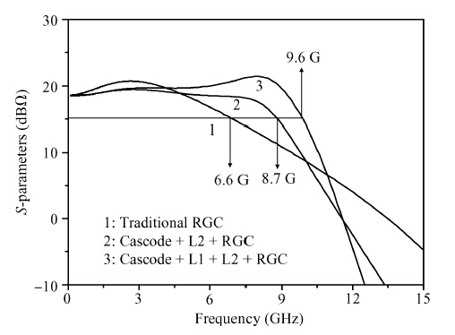
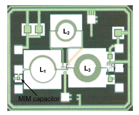
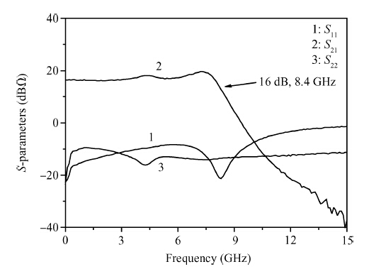
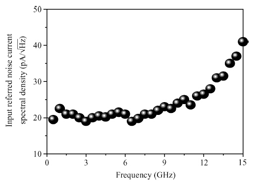
This paper presents a modified regulated cascode (RGC) transimpedance amplifier (TIA) with a novel pre-equalized technique. The pre-equalized circuit employed the broadband series inductive π-network and Gm-boosting technique. The introduction of this technique compensates the transferred signal at the input port of the TIA without an increase in power dissipation. Furthermore, a novel miller capacitance degeneration method is designed in the gain stage for further bandwidth improvement. The TIA is realized in UMC 0.18 μm CMOS technology and tested with an on-chip 0.3 pF capacitor to emulate a photodetector (PD). The measured transimpedance gain amounts to 57 dBΩ with a -3 dB bandwidth of about 8.2 GHz and consumes only 22 mW power from a single 1.8 V supply.


J. Semicond.
2015, 36(7): 075003 doi: 10.1088/1674-4926/36/7/075003

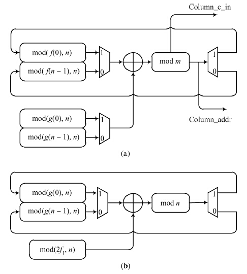
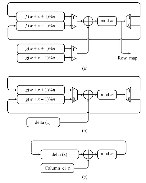
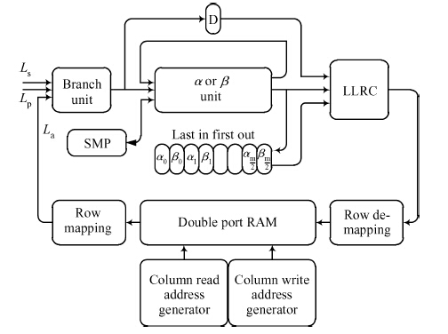
This paper presents a turbo decoder supporting all 188 block sizes in 3GPP long term evolution (LTE) standard which can be employed in the LTE micro-eNodB system. The design allows 1, 2, 4, 8 or 16 soft-in/soft-out (SISO) decoders to concurrently process each block size, and the number of iterations can be adjusted. This article proposes an improved SISO algorithm and interleaving design, calculated forward state matrix and backward state matrix alternately, and the branch transition probability can be used in the Turbo decode process directly just after one clock delay. The structure enables a decoder processing radix-2 algorithm with high speed, instead of radix-4 as the conventional decoder. Moreover, the paper details an interleaver/de-interleaver, which is combined by two operational steps. One is column address mapping and the other is intra-row permutation. Decoder realizes interleaving by loading data from memories whose address is generated by column mapping and then lets data passing through inter-row permutation. For de-interleaving, the system can adopt reverse operation.


J. Semicond.
2015, 36(7): 075004 doi: 10.1088/1674-4926/36/7/075004

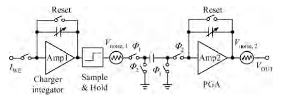
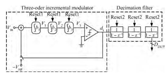
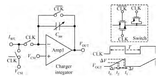
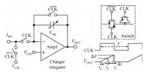
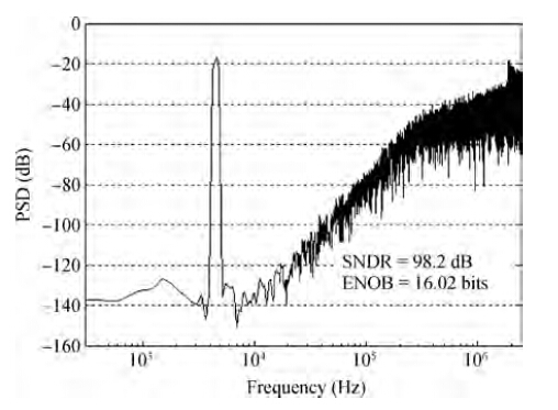
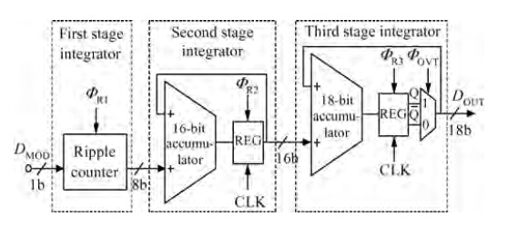
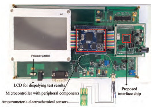
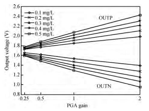
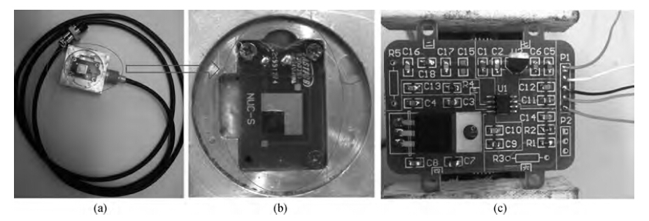
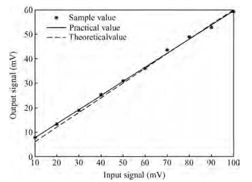
This paper reports a complimentary metal-oxide-semiconductor (CMOS) analog front-end chip for amperometric electrochemical sensors. The chip includes a digital configuration circuit, which can communicate with an external microcontroller by employing an I2C interface bus, and thus is highly programmable. Digital correlative double samples technique and an incremental sigma-delta analog to digital converter (Σ-Δ ADC) are employed to achieve a new proposed system architecture with double samples. The chip has been fabricated in a standard 0.18-μm CMOS process with high-precision and high-linearity performance occupying an area of 1.3 × 1.9 mm2. Sample solutions with various phosphate concentrations have been detected with a step concentration of 0.01 mg/L.


J. Semicond.
2015, 36(7): 075005 doi: 10.1088/1674-4926/36/7/075005

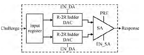
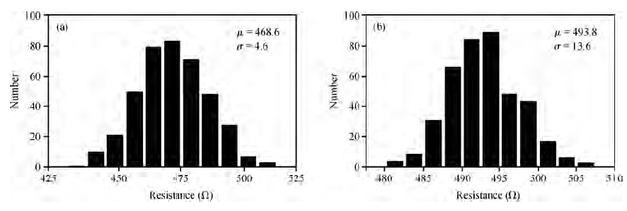
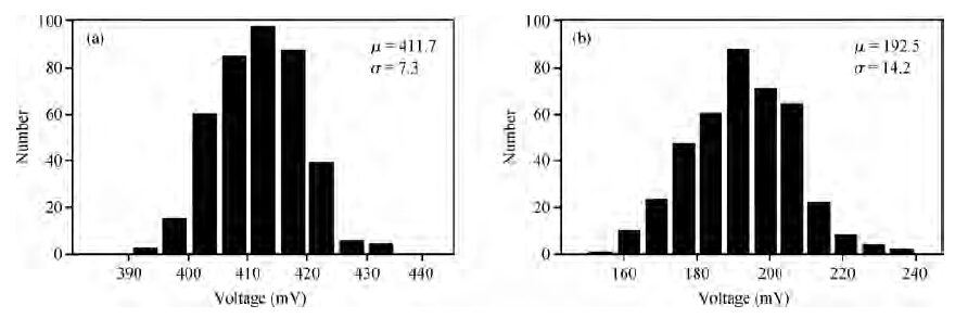
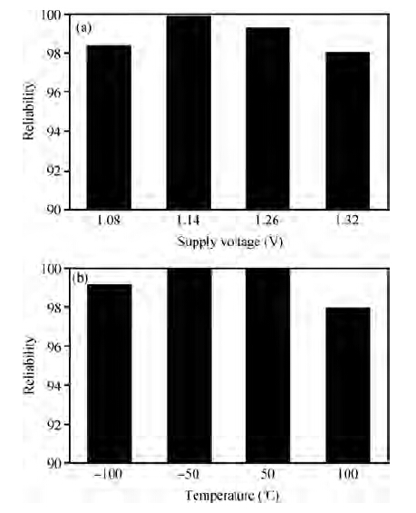
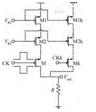
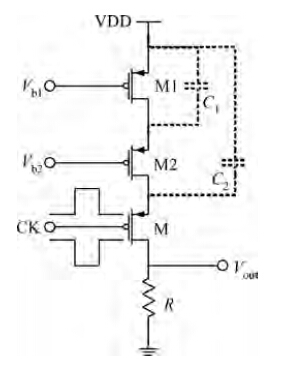
A novel physical unclonable functions (PUF) circuit is proposed, which relies on non-linear characteristic of analog voltage generated by R-2R ladder DAC. After amplifying the deviation signal, the robustness of the DAC-PUF circuit has increased significantly. The DAC-PUF circuit is designed in TSMC 65 nm CMOS technology and the layout occupies 86.06 × 63.56 μm2. Monte Carlo simulation results show that the reliability of the DAC-PUF circuit is above 98% over a comprehensive range of environmental variation, such as temperature and supply voltage.


J. Semicond.
2015, 36(7): 075006 doi: 10.1088/1674-4926/36/7/075006

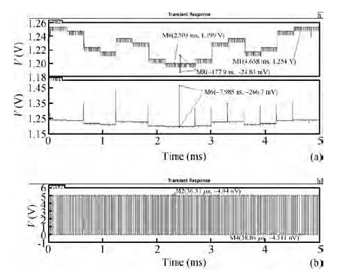
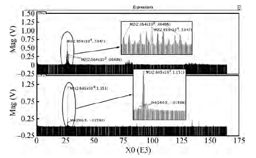
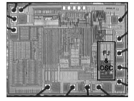
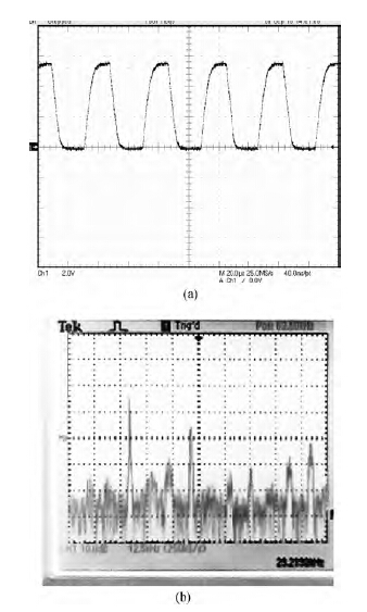
The digital-to-analogue converter (DAC) plays a significant role in modern electronic systems, and current-mode DACs are widely used due to their excellent properties. However, the non-ideal transition at switching instants of the unit circuit will directly affect the performance of the current-mode DAC. The parasitic effects resulting in non-ideal transition are analyzed in this paper. A simple structure unit circuit is proposed to diminish the non-ideal transition. The simulation results show that the parasitic effects are suppressed effectively, and a smoother output transition is achieved. The feasibility of the proposed current-mode DAC unit circuit is verified by the application in a frequency jitter circuit.

J. Semicond.
2015, 36(7): 075007 doi: 10.1088/1674-4926/36/7/075007

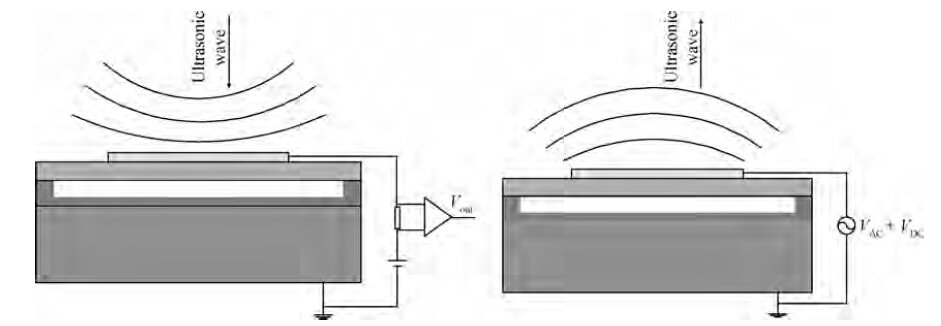
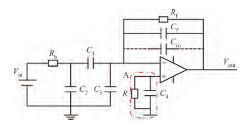
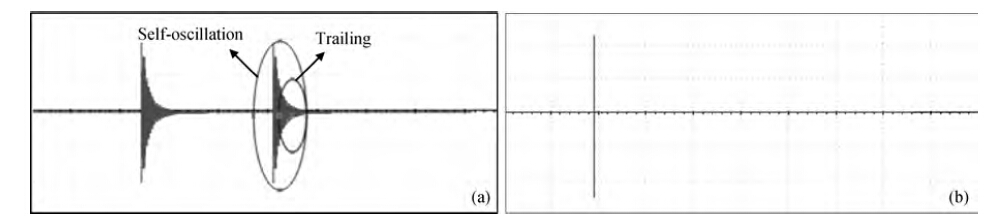
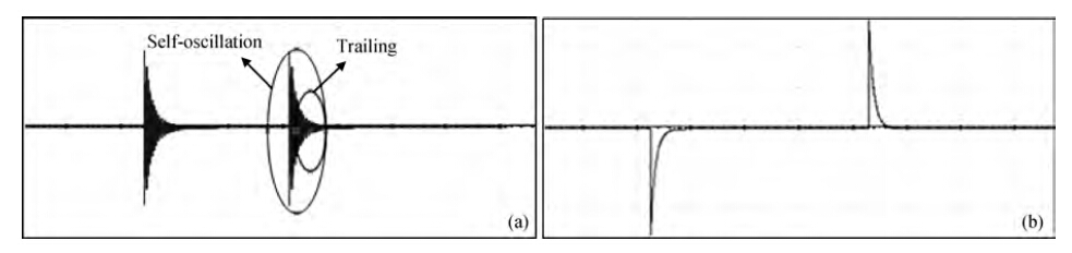
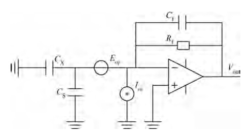
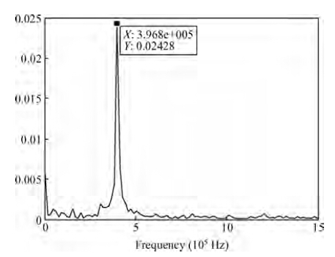
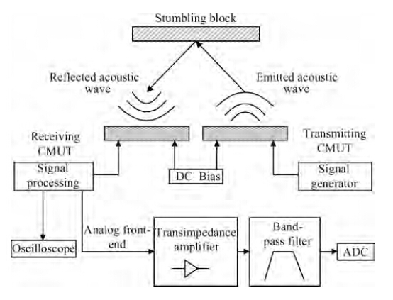
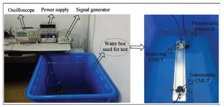
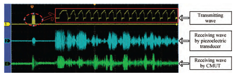
This paper presents a transimpedance amplifier (TIA) capacitance detection circuit aimed at detecting micro-capacitance, which is caused by ultrasonic stimulation applied to the capacitive micro-machined ultrasonic transducer (CMUT). In the capacitance interface, a TIA is adopted to amplify the received signal with a center frequency of 400 kHz, and finally detect ultrasound pressure. The circuit has a strong anti-stray property and this paper also studies the calculation of compensation capacity in detail. To ensure high resolution, noise analysis is conducted. After optimization, the detected minimum ultrasound pressure is 2.1 Pa, which is two orders of magnitude higher than the former. The test results showed that the circuit was sensitive to changes in ultrasound pressure and the distance between the CMUT and stumbling block, which also successfully demonstrates the functionality of the developed TIA of the analog-front-end receiver.
J. Semicond.
2015, 36(7): 076001 doi: 10.1088/1674-4926/36/7/076001

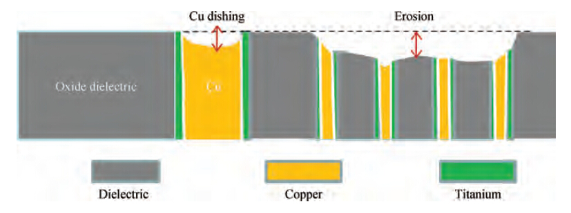
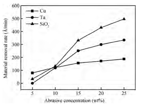
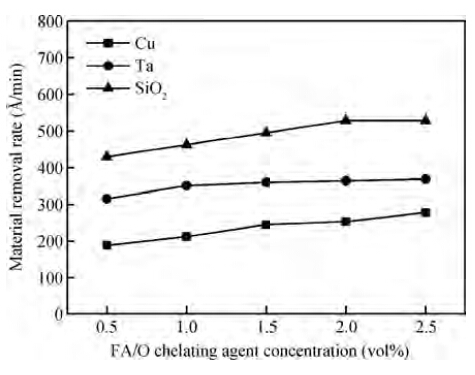
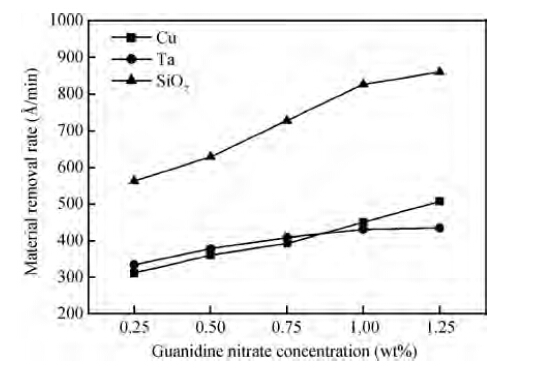
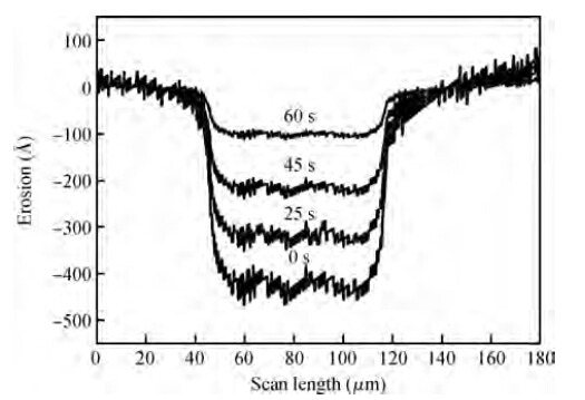
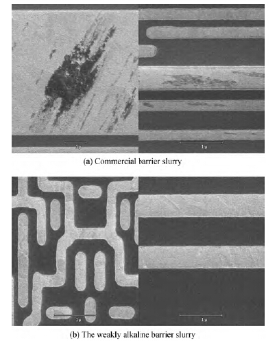
Controllable removal rate selectivity with various films (Cu, Ta, SiO2) is a challenging job in barrier CMP. H2O2 as an oxidizer and benzotriazole (BTA) as an inhibitor is considered to be an effective method in barrier CMP. Slurries that contain hydrogen peroxide have a very short shelf life because H2O2 is unstable and easily decomposed. BTA can cause post-CMP challenges, such as organic residue, toxicity and particle adhesion. We have been engaged in studying a weakly alkaline barrier slurry without oxidizer and benzotriazole. Based on these works, the objective of this paper is to discuss the mechanism of the development of the barrier slurry without oxidizer and benzotriazole by studying the effects of the different components (containing colloidal silica, FA/O complexing agent, pH of polishing solution and guanidine nitrate) on removal rate selectivity. The possible related polishing mechanism has also been proposed.

J. Semicond.
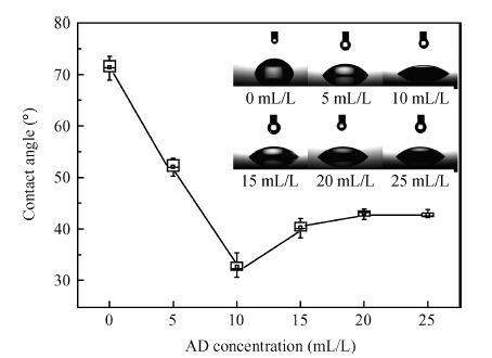
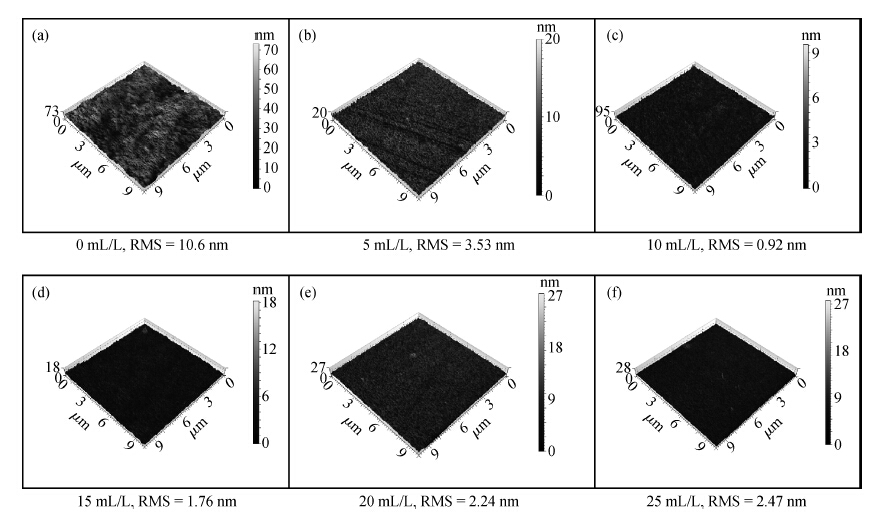
2015, 36(7): 076002 doi: 10.1088/1674-4926/36/7/076002

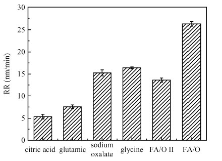
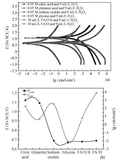
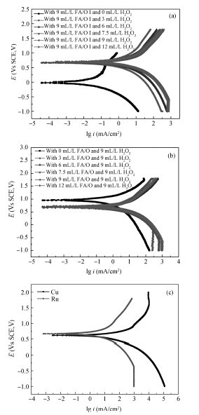
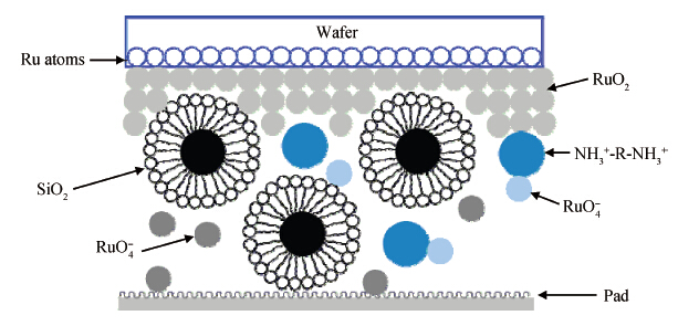
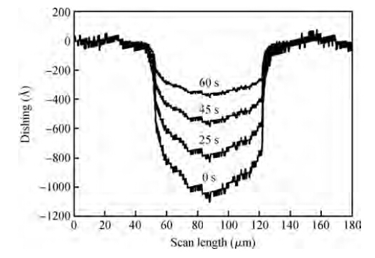
This paper investigated the effect of FA/O and hydrogen peroxide (H2O2) on ruthenium (Ru) removal rate (RR) and static etching rate (SER). It was revealed that Ru RR and SER first linearly increased then slowly decreaseed with the increasing H2O2 probably due to the formation of uniform Ru oxides on the surface during polishing. Their corrosion behaviors and states of surface oxidation were analyzed. In addition, FA/O could chelate Ru oxides (such as (RuO4)2- and RuO4- changed into soluble amine salts [R(NH3)4] (RuO4)2) and enhance Ru RR. The non-ionic surfactant AD was used to improve the Ru CMP performance. In particular, the addition of AD can lead to significant improvement of the surface roughness.