


Device scaling is an important part of the very large scale integration (VLSI) design to boost up the success path of VLSI industry, which results in denser and faster integration of the devices. As technology node moves towards the very deep submicron region, leakage current and circuit reliability become the key issues. Both are increasing with the new technology generation and affecting the performance of the overall logic circuit. The VLSI designers must keep the balance in power dissipation and the circuit's performance with scaling of the devices. In this paper, different scaling methods are studied first. These scaling methods are used to identify the effects of those scaling methods on the power dissipation and propagation delay of the CMOS buffer circuit. For mitigating the power dissipation in scaled devices, we have proposed a reliable leakage reduction low power transmission gate (LPTG) approach and tested it on complementary metal oxide semiconductor (CMOS) buffer circuit. All simulation results are taken on HSPICE tool with Berkeley predictive technology model (BPTM) BSIM4 bulk CMOS files. The LPTG CMOS buffer reduces 95.16% power dissipation with 84.20% improvement in figure of merit at 32 nm technology node. Various process, voltage and temperature variations are analyzed for proving the robustness of the proposed approach. Leakage current uncertainty decreases from 0.91 to 0.43 in the CMOS buffer circuit that causes large circuit reliability.

One of the core semiconductor devices is the electrostatic chuck. It has been widely used in plasma-based and vacuum-based semiconductor processing. The electrostatic chuck plays an important role in adsorbing and cooling/heating wafers, and has technical advantages on non-edge exclusion, high reliability, wafer planarity, particles reduction and so on. This article extracts key design elements from the existing knowledge and techniques of electrostatic chuck by the method proposed by Paul and Beitz, and establishes a design space systematically. The design space is composed of working objects, working principles and working structures. The working objects involve electrostatic chuck components and materials, classifications, and relevant properties; the working principles involve clamping force, residual force, and temperature control; the working structures describe how to compose an electrostatic chuck and to fulfill the overall functions. The systematic design space exhibits the main issues during electrostatic chuck design. The design space will facilitate and inspire designers to improve the design quality and shorten the design time in the conceptual design.

Since the invention of amorphous indium–gallium–zinc–oxide (IGZO) based thin-film transistors (TFTs) by Hideo Hosono in 2004, investigations on the topic of IGZO TFTs have been rapidly expanded thanks to their high electrical performance, large-area uniformity, and low processing temperature. This article reviews the recent progress and major trends in the field of IGZO-based TFTs. After a brief introduction of the history of IGZO and the main advantages of IGZO-based TFTs, an overview of IGZO materials and IGZO-based TFTs is given. In this part, IGZO material electron travelling orbitals and deposition methods are introduced, and the specific device structures and electrical performance are also presented. Afterwards, the recent advances of IGZO-based TFT applications are summarized, including flat panel display drivers, novel sensors, and emerging neuromorphic systems. In particular, the realization of flexible electronic systems is discussed. The last part of this review consists of the conclusions and gives an outlook over the field with a prediction for the future.

In this work, we design and fabricate a deep ultraviolet (DUV) light-emitting array consisting of 10 × 10 micro-LEDs (μ-LEDs) with each device having 20 μm in diameter. Strikingly, the array demonstrates a significant enhancement of total light output power by nearly 52% at the injection current of 100 mA, in comparison to a conventional large LED chip whose emitting area is the same as the array. A much higher (~22%) peak external quantum efficiency, as well as a smaller efficiency droop for μ-LED array, was also achieved. The numerical calculation reveals that the performance boost can be attributed to the higher light extraction efficiency at the edge of each μ-LED. Additionally, the far-field pattern measurement shows that the μ-LED array possesses a better forward directionality of emission. These findings shed light on the enhancement of the DUV LEDs performance and provide new insights in controlling the light behavior of the μ-LEDs.
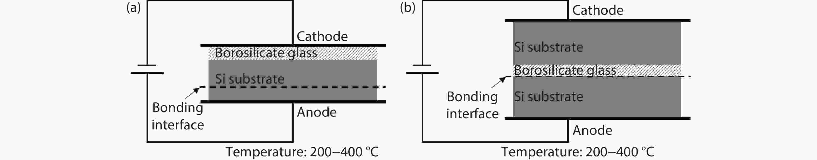
The heterogeneous integration of III–V devices with Si-CMOS on a common Si platform has shown great promise in the new generations of electrical and optical systems for novel applications, such as HEMT or LED with integrated control circuitry. For heterogeneous integration, direct wafer bonding (DWB) techniques can overcome the materials and thermal mismatch issues by directly bonding dissimilar materials systems and device structures together. In addition, DWB can perform at wafer-level, which eases the requirements for integration alignment and increases the scalability for volume production. In this paper, a brief review of the different bonding technologies is discussed. After that, three main DWB techniques of single-, double- and multi-bonding are presented with the demonstrations of various heterogeneous integration applications. Meanwhile, the integration challenges, such as micro-defects, surface roughness and bonding yield are discussed in detail.
Due to the excellent optoelectronic properties, fast response time, outstanding power efficiency and high stability, micro-LED plays an increasingly important role in the new generation of display technology compared with LCD and OLED display. This paper mainly introduces the preparation methods of the GaN-based micro-LED array, the optoelectronic characteristics, and several key technologies to achieve full-color display, such as transfer printing, color conversion by quantum dot and local strain engineering.

This paper presents a review and discussion for high-speed photodetectors and their applications on optical communications and microwave photonics. A detailed and comprehensive demonstration of high-speed photodetectors from development history, research hotspots to packaging technologies is provided to the best of our knowledge. A few typical applications based on photodetectors are also illustrated, such as free-space optical communications, radio over fiber and millimeter terahertz signal generation systems.
Memristors are now becoming a prominent candidate to serve as the building blocks of non-von Neumann in-memory computing architectures. By mapping analog numerical matrices into memristor crossbar arrays, efficient multiply accumulate operations can be performed in a massively parallel fashion using the physics mechanisms of Ohm’s law and Kirchhoff’s law. In this brief review, we present the recent progress in two niche applications: neural network accelerators and numerical computing units, mainly focusing on the advances in hardware demonstrations. The former one is regarded as soft computing since it can tolerant some degree of the device and array imperfections. The acceleration of multiple layer perceptrons, convolutional neural networks, generative adversarial networks, and long short-term memory neural networks are described. The latter one is hard computing because the solving of numerical problems requires high-precision devices. Several breakthroughs in memristive equation solvers with improved computation accuracies are highlighted. Besides, other nonvolatile devices with the capability of analog computing are also briefly introduced. Finally, we conclude the review with discussions on the challenges and opportunities for future research toward realizing memristive analog computing machines.
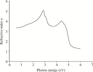
We have investigated the optical properties of gallium arsenide (GaAs) in the photon energy range 0.6-6.0 eV. We obtained a refractive index which has a maximum value of 5.0 at a photon energy of 3.1 eV; an extinction coefficient which has a maximum value of 4.2 at a photon energy of 5.0 eV; the dielectric constant, the real part of the complex dielectric constant has a maximum value of 24 at a photon energy of 2.8 eV and the imaginary part of the complex dielectric constant has a maximum value of 26.0 at a photon energy of 4.8 eV; the transmittance which has a maximum value of 0.22 at a photon energy of 4.0 eV; the absorption coefficient which has a maximum value of 0.22×10⁸ m-1 at a photon energy of 4.8 eV, the reflectance which has a maximum value of 0.68 at 5.2eV; the reflection coefficient which has a maximum value of 0.82 at a photon energy of 5.2 eV; the real part of optical conductivity has a maximum value of 14.2×10¹⁵ at 4.8 eV and the imaginary part of the optical conductivity has a maximum value of 6.8×10¹⁵ at 5.0 eV. The values obtained for the optical properties of GaAs are in good agreement with other results.
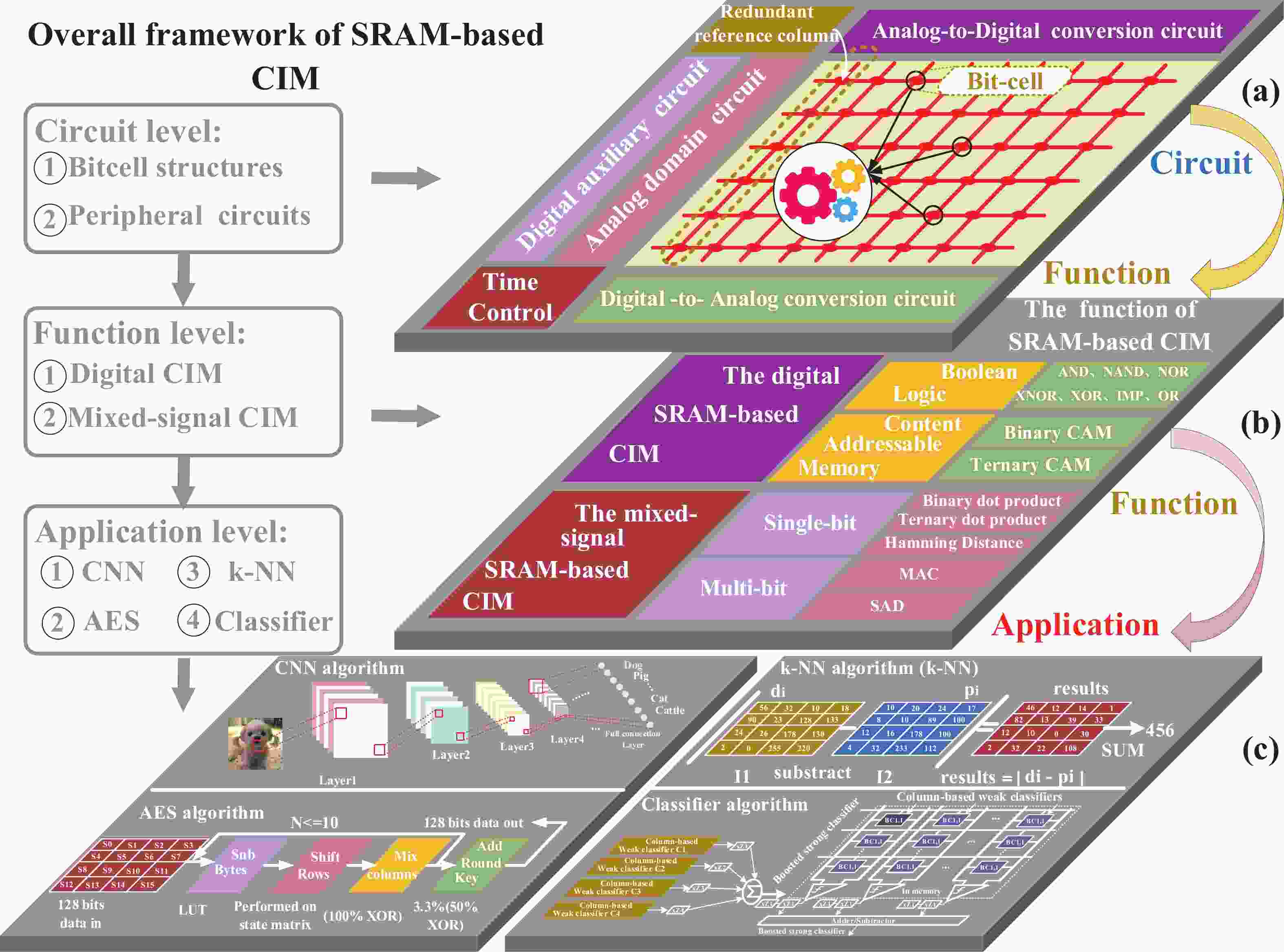
Artificial intelligence (AI) processes data-centric applications with minimal effort. However, it poses new challenges to system design in terms of computational speed and energy efficiency. The traditional von Neumann architecture cannot meet the requirements of heavily data-centric applications due to the separation of computation and storage. The emergence of computing in-memory (CIM) is significant in circumventing the von Neumann bottleneck. A commercialized memory architecture, static random-access memory (SRAM), is fast and robust, consumes less power, and is compatible with state-of-the-art technology. This study investigates the research progress of SRAM-based CIM technology in three levels: circuit, function, and application. It also outlines the problems, challenges, and prospects of SRAM-based CIM macros.
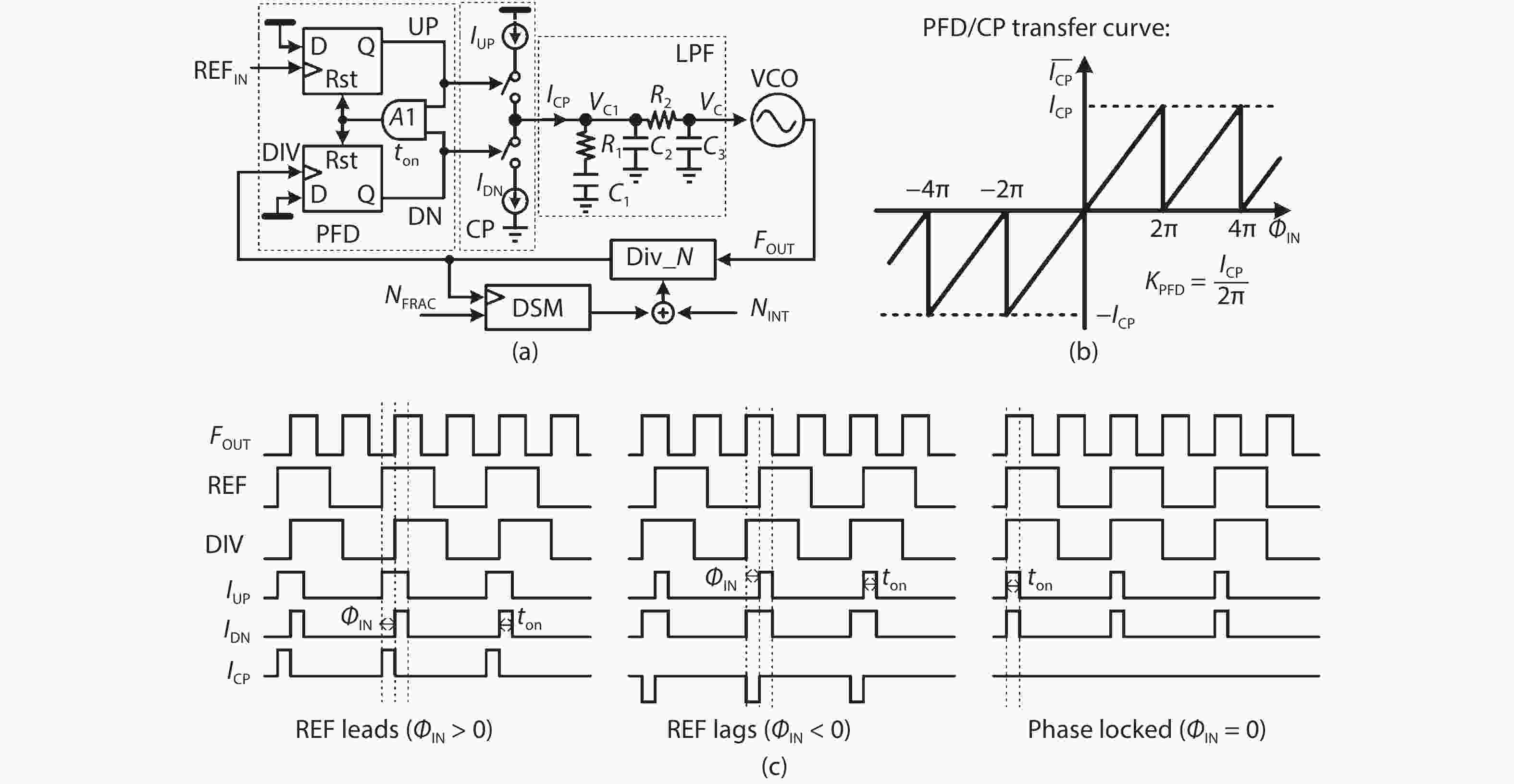
CMOS analog and mixed-signal phase-locked loops (PLL) are widely used in varies of the system-on-chips (SoC) as the clock generator or frequency synthesizer. This paper presents an overview of the AMS-PLL, including: 1) a brief introduction of the basics of the charge-pump based PLL, which is the most widely used AMS-PLL architecture due to its simplicity and robustness; 2) a summary of the design issues of the basic CPPLL architecture; 3) a systematic introduction of the techniques for the performance enhancement of the CPPLL; 4) a brief overview of ultra-low-jitter AMS-PLL architectures which can achieve lower jitter (< 100 fs) with lower power consumption compared with the CPPLL, including the injection-locked PLL (ILPLL), sub-sampling (SSPLL) and sampling PLL (SPLL); 5) a discussion about the consideration of the AMS-PLL architecture selection, which could help designers meet their performance requirements.

The super junction (SJ) has been recognized as the " milestone” of the power MOSFET, which is the most important innovation concept of the voltage-sustaining layer (VSL). The basic structure of the SJ is a typical junction-type VSL (J-VSL) with the periodic N and P regions. However, the conventional VSL is a typical resistance-type VSL (R-VSL) with only an N or P region. It is a qualitative change of the VSL from the R-VSL to the J-VSL, introducing the bulk depletion to increase the doping concentration and optimize the bulk electric field of the SJ. This paper firstly summarizes the development of the SJ, and then the optimization theory of the SJ is discussed for both the vertical and the lateral devices, including the non-full depletion mode, the minimum specific on-resistance optimization method and the equivalent substrate model. The SJ concept breaks the conventional " silicon limit” relationship of Ron∝VB2.5, showing a quasi-linear relationship of Ron∝VB1.03.
Hybrid white micro-pillar structure light emitting diodes (LEDs) have been manufacture utilizing blue micro-LEDs arrays integrated with 580 nm CIS ((CuInS2-ZnS)/ZnS) core/shell quantum dots. The fabricated hybrid white micro-LEDs have good electrical properties, which are manifested in relatively low turn-on voltage and reverse leakage current. High-quality hybrid white light emission has been demonstrated by the hybrid white micro-LEDs after a systemic optimization, in which the corresponding color coordinates are calculated to be (0.3303, 0.3501) and the calculated color temperature is 5596 K. This result indicates an effective way to achieve high-performance white LEDs and shows great promise in a large range of applications in the future including micro-displays, bioinstrumentation and visible light communication.
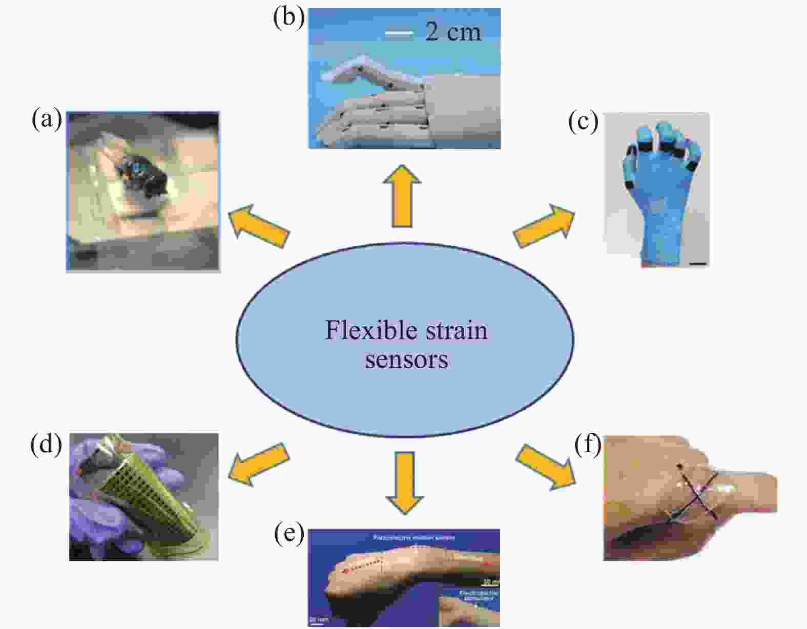
With the rapid development of human artificial intelligence and the inevitably expanding markets, the past two decades have witnessed an urgent demand for the flexible and wearable devices, especially the flexible strain sensors. Flexible strain sensors, incorporated the merits of stretchability, high sensitivity and skin-mountable, are emerging as an extremely charming domain in virtue of their promising applications in artificial intelligent realms, human-machine systems and health-care devices. In this review, we concentrate on the transduction mechanisms, building blocks of flexible physical sensors, subsequently property optimization in terms of device structures and sensing materials in the direction of practical applications. Perspectives on the existing challenges are also highlighted in the end.
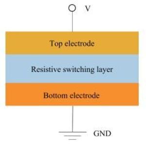
The resistive random access memory (RRAM) device has been widely studied due to its excellent memory characteristics and great application potential in different fields. In this paper, resistive switching materials, switching mechanism, and memory characteristics of RRAM are discussed. Recent research progress of RRAM in high-density storage and nonvolatile logic application are addressed. Technological trends are also discussed.
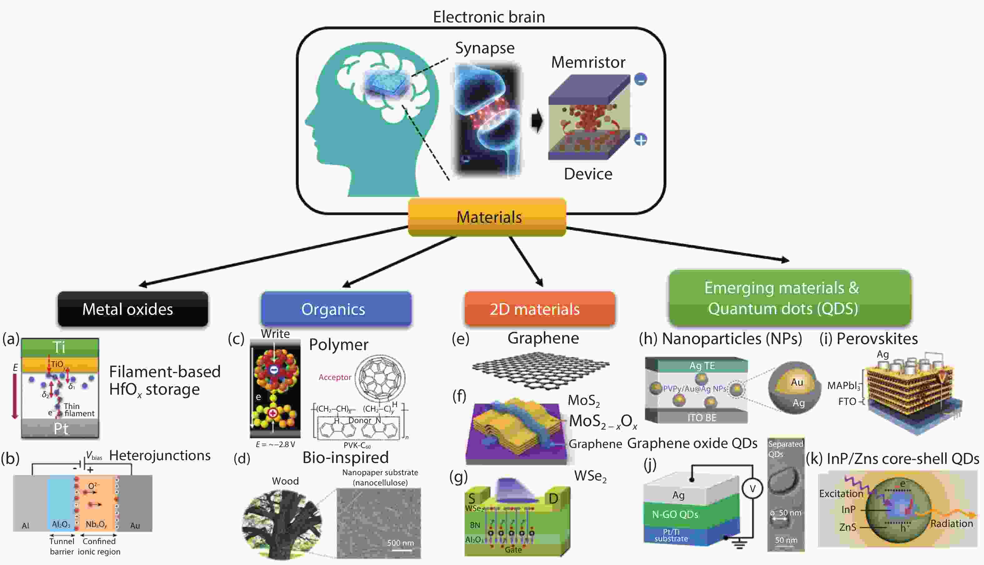
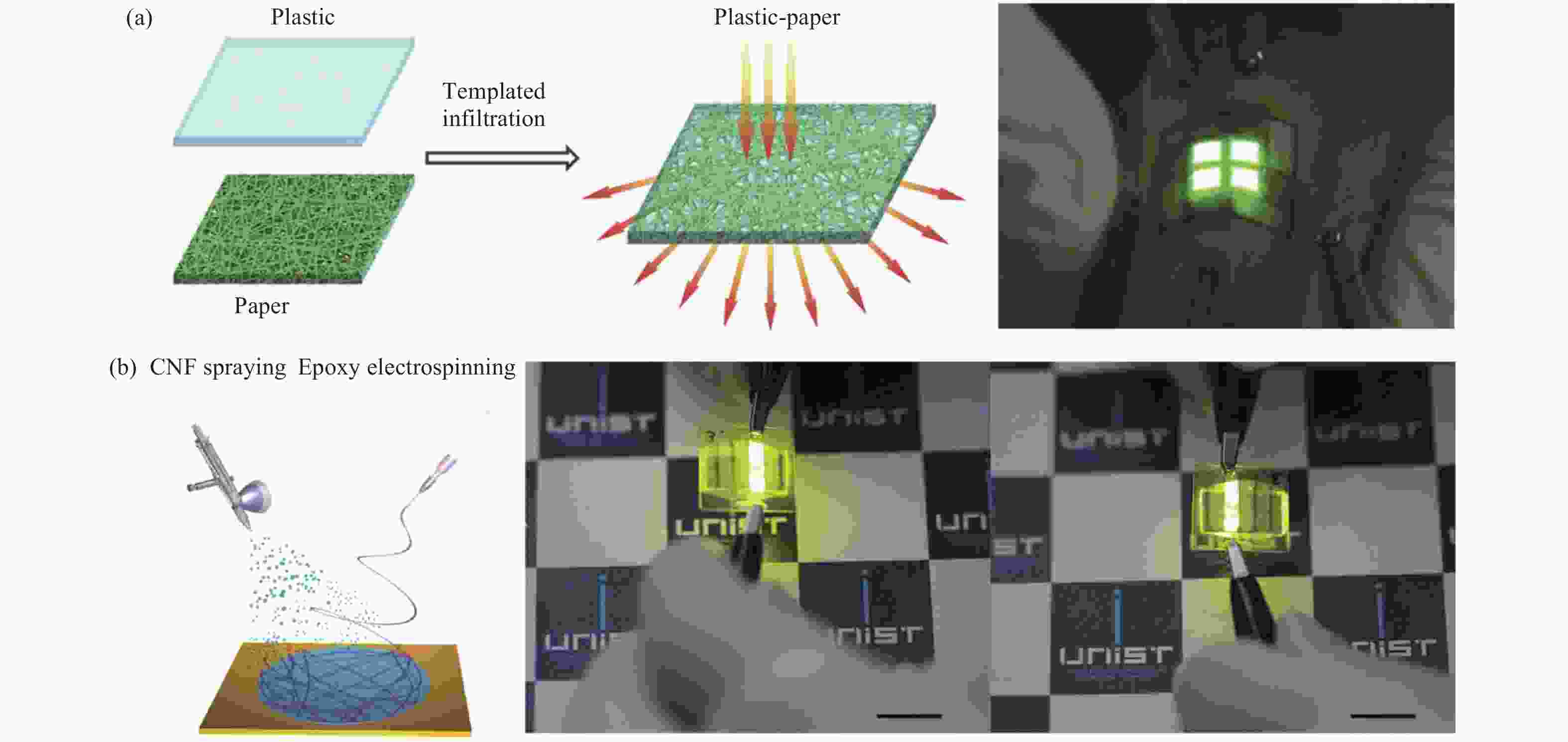
Resistive random-access memory (RRAM), also known as memristors, having a very simple device structure with two terminals, fulfill almost all of the fundamental requirements of volatile memory, nonvolatile memory, and neuromorphic characteristics. Its memory and neuromorphic behaviors are currently being explored in relation to a range of materials, such as biological materials, perovskites, 2D materials, and transition metal oxides. In this review, we discuss the different electrical behaviors exhibited by RRAM devices based on these materials by briefly explaining their corresponding switching mechanisms. We then discuss emergent memory technologies using memristors, together with its potential neuromorphic applications, by elucidating the different material engineering techniques used during device fabrication to improve the memory and neuromorphic performance of devices, in areas such as ION/IOFF ratio, endurance, spike time-dependent plasticity (STDP), and paired-pulse facilitation (PPF), among others. The emulation of essential biological synaptic functions realized in various switching materials, including inorganic metal oxides and new organic materials, as well as diverse device structures such as single-layer and multilayer hetero-structured devices, and crossbar arrays, is analyzed in detail. Finally, we discuss current challenges and future prospects for the development of inorganic and new materials-based memristors.
Flexible and wearable optoelectronic devices have been developing to a new stage due to their unique capacity for the possibility of a variety of wearable intelligent electronics, including bendable smartphones, foldable touch screens and antennas, paper-like displays, and curved and flexible solid-state lighting devices. Before extensive commercial applications, some issues still have to be solved for flexible and wearable optoelectronic devices. In this regard, this review concludes the newly emerging flexible substrate materials, transparent conductive electrodes, device architectures and light manipulation methods. Examples of these components applied for various kinds of devices are also summarized. Finally, perspectives about the bright future of flexible and wearable electronic devices are proposed.
Recently, many groups have focused on the development of GaN-based green LDs to meet the demand for laser display. Great progresses have been achieved in the past few years even that many challenges exist. In this article, we analysis the challenges to develop GaN-based green LDs, and then the approaches to improve the green LD structure in the aspect of crystalline quality, electrical properties, and epitaxial layer structure are reviewed, especially the work we have done.
The rapid development of bulk β-Ga2O3 crystals has attracted much attention to their use as ultra-wide bandgap materials for next-generation power devices owing to its large bandgap (~ 4.9 eV) and large breakdown electric field of about 8 MV/cm. Low cost and high quality of large β-Ga2O3 single-crystal substrates can be attained by melting growth techniques widely used in the industry. In this paper, we first present an overview of the properties of β-Ga2O3 crystals in bulk form. We then describe the various methods for producing bulk β-Ga2O3 crystals and their applications. Finally, we will present a future perspective of the research in the area in the area of single crystal growth.
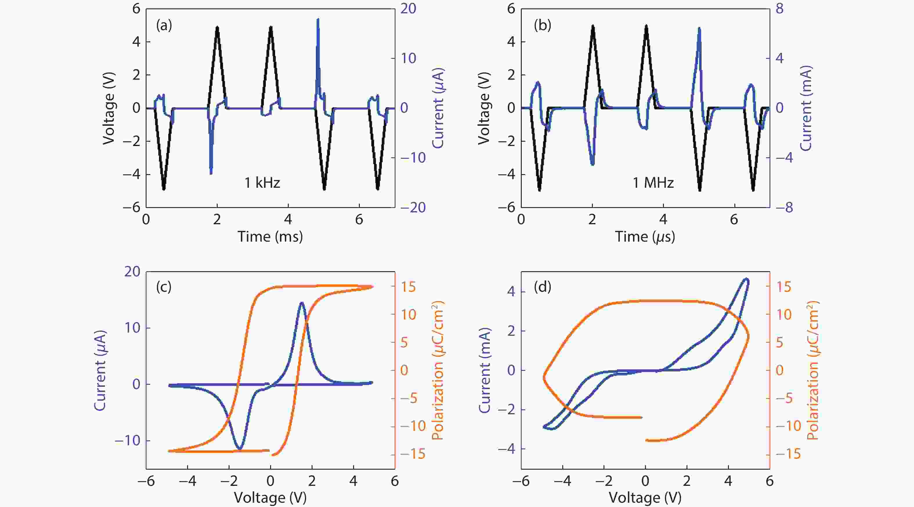
Ferroelectric hysteresis loop measurement under high driving frequency generally faces great challenges. Parasitic factors in testing circuits such as leakage current and RC delay could result in abnormal hysteresis loops with erroneous remnant polarization (Pr) and coercive field (Ec). In this study, positive-up-negative-down (PUND) measurement under a wide frequency range was performed on a 10-nm thick Hf0.5Zr0.5O2 ferroelectric film. Detailed analysis on the leakage current and RC delay was conducted as the polarization switching occurs in the FE capacitor. After considering the time lag caused by RC delay, reasonable calibration of current response over the voltage pulse stimulus was employed in the integral of polarization current over time. In such a method, rational P–V loops measured at high frequencies (>1 MHz) was successfully achieved. This work provides a comprehensive understanding on the effect of parasitic factors on the polarization switching behavior of FE films.
- First
- Prev
- 1
- 2
- 3
- 4
- 5
- Next
- Last
- Total: 5
- To
- Go


