According to the international technology roadmap for semiconductors (ITRS),32nm technology node will be introduced around 2009.Scaling of CMOS logic devices from 45 to 32nm node has come across significant barriers.Overcoming these pitch-scaling induced barriers requires integrating the most advanced process technologies into product manufacturing.This paper reviews and discusses new technology applications that could be potentially integrated into 32nm node in the following areas:extension of immersion lithography,mobility enhancement substrate technology,metal/high-k (MHK) gate stack,ultra-shallow junction (USJ) and other strain enhancement engineering methods,including stress proximity effect (SPT),dual stress liner (DSL),stress memorization technique (SMT),high aspect ratio process (HARP) for STI and PMD,embedded SiGe (for pFET) and SiC (for nFET) source/drain (S/D) using selective epitaxial growth (SEG) method,metallization for middle of line (MOL) and back-end of line (BEOL),and ultra low-k (ULK) integration.
We propose and fabricate an AlGaN/GaN high electron mobility transistor (HEMT) on sapphire substrate using a new kind of electron beam (EB) lithography layout for the T-gate.Using this new layout,we can change the aspect ratio (ratio of top gate dimension to gate length) and modify the shape of the T-gate freely.Therefore,we obtain a 0.18μm gate-length AlGaN/GaN HEMT with a unity current gain cutoff frequency (fT) of 65GHz.The aspect ratio of the T-gate is 10.These single finger devices also exhibit a peak extrinsic transconductance of 287mS/mm and a maximum drain current as high as 980mA/mm.
This paper presents an SG-DBR with a monolithically integrated SOA fabricated using quantum-well intermixing (QWI) for the first time in mainland China.The wavelength tuning range covers 33nm and the output power reaches 10mW with an SOA current of 50mA.The device can work at available channels with SMSR over 35dB.
We investigate the contact characteristics of bi-layer thin films,Ti(20nm)/Al(200nm) on Si-doped n-type Al0.6Ga0.4N films grown on sapphire substrate.The surface treatment was aqua regia boiling before metallization and annealing after metallization at different conditions in N2 ambient.High resolution X-ray diffractometery analysis was carried out on the contacts and the surface interfaces of these conditions were compared.A specific contact resistivity ρc was determined using the circular transmission line method via current-voltage measurements.A ρc of 3.42E-4 Ω·cm2 was achieved when annealed at 670℃ for 90s.Then,this ideal ohmic contact was used in back-illuminated solar-blind AlGaN p-i-n detectors and the detectors’ performances,such as spectral responsivity,dark-current,and breakdown voltage were optimized.
We describe the fabrication of metal nanogaps of sub-20nm in feature size using the proximity effect in electron beam lithography (EBL).The proximity effect is extended to develop a flexible and practical method for preparing metal (e.g.Au or Ag) nanogaps and arrays in combination with a transfer process (e.g.,deposition/lift-off).Different from the direct gap-writing process,the nanogap precursor structures (nanoconnections) were designed by GDSII software and then written by electron beam.Following a deposition and lift-off process,the metal nanogaps were obtained and the nanogap size can be lowered to ~10nm by controlling the exposure dose in EBL.
A band edge model in (101)-biaxial strained Si on relaxed Si1-xGex alloy,or monoclinic Si (m-Si),is presented using the k·p perturbation method coupled with deformation potential theory.Results show that the [001],[001],[100],[100] valleys constitute the conduction band (CB) edge,which moves up in electron energy as the Ge fraction (x) increases.Furthermore,the CB splitting energy is in direct proportion to x and all the valence band (VB) edges move up in electron energy as x increases.In addition,the decrease in the indirect bandgap and the increase in the VB edge splitting energy as x increases are found.The quantitative data from the models supply valuable references for the design of the devices.
Phosphorus was diffused into CVT grown undoped ZnO bulk single crystals at 550 and 800℃ in a closed quartz tube.The P-diffused ZnO single crystals were characterized by the Hall effect,X-ray photoelectron spectroscopy (XPS),photoluminescence spectroscopy (PL),and Raman scattering.The P-diffused ZnO single crystals are n-type and have higher free electron concentration than undoped ZnO,especially for the sample diffused at 800℃.The PL measurement reveals defect related visible broad emissions in the range of 420~550nm in the P-diffused ZnO samples.The XPS result suggests that most of the P atoms substitute in the Zn site after they diffuse into the ZnO single crystal at 550℃,while the P atom seems to occupy the O site in the ZnO samples diffused at 800℃.A high concentration of shallow donor defect forms in the P-diffused ZnO,resulting in an apparent increase of free electron concentration.
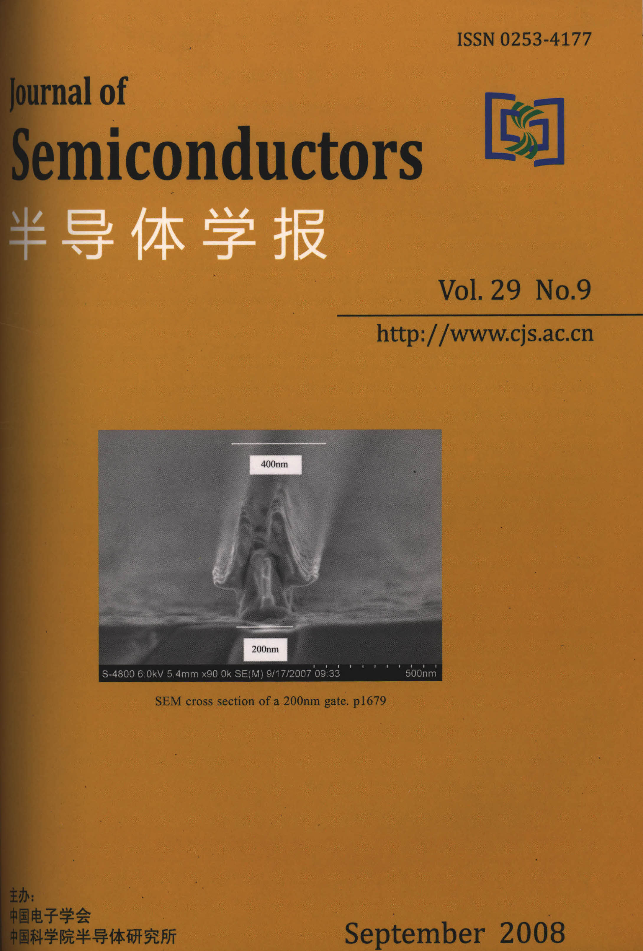
200nm gate-length GaAs-based InAlAs/InGaAs MHEMTs are fabricated by MBE epitaxial material and EBL (electron beam lithography) technology.Ti/Pt/Au is evaporated to form gate metals.A T-shaped gate is produced using a novel PMMA/PMGI/PMMA trilayer resist structure to decrease parasitic capacitance and parasitic resistance of the gate.Excellent DC and RF performances are obtained and the transconductance (gm),maximum saturation drain current density (JDSS),threshold voltage (VT),current cut-off frequency (fT),and maximum oscillation frequency (fmax) of InAlAs/InGaAs MHEMTs are 510mS/mm,605mA/mm,-1.8V,110GHz,and 72GHz,respectively.
Fabrication of enhancement-mode high electron mobility transistors on AlGaN/GaN heterostructures grown on sapphire substrates is reported.These devices with 1.2μm gate-length,4mm space between source and drain,and 15nm recessed-gate depth exhibit a maximum drain current of 332mA/mm at 3V,a maximum transconductance of 221mS/mm,a threshold voltage of 0.57V, ft of 5.2GHz,and fmax of 9.3GHz.A dielectric layer formed unintentionally during recessed-gate etching is confirmed by contrasting the Schottky I-V characteristics of pre-etching and post-etching.The frequency characteristics and subthreshold characteristics of the devices are studied in detail.
A Geiger mode planar InGaAs/InP avalanche photodiode (APD) with a cascade peripheral junction structure to suppress edge breakdowns is designed by finite-element analysis.The photodiode breakdown voltage is reduced to 54.3V by controlling the central junction depth,while the electric field distribution along the device central axis is controlled by adjusting doping level and thickness of the InP field control layer.Using a cascade junction structure at the periphery of the active area,premature edge breakdowns are effectively suppressed.The simulations show that the quadra-cascade structure is a good trade-off between suppression performance and fabrication complexity,with a reduced peak electric field of 5.2E5kV/cm and a maximum hole ionization integral of 1.201.Work presented in this paper provides an effective way to design high performance photon counting InGaAs/InP avalanche photodiodes.
Single event transient of a real p-n junction in a 0.18μm bulk process is studied by 3D TCAD simulation.The impact of voltage,temperature,substrate concentration,and LET on SET is studied.Our simulation results demonstrate that biases in the range 1.62 to 1.98V influence DSET current shape greatly and total collected charge weakly.Peak current and charge collection within 2ns decreases as temperature increases,and temperature has a stronger influence on SET currents than on total charge.Typical variation of substrate concentration in modern VDSM processes has a negligible effect on SEEs.Both peak current and total collection charge increases as LET increases.
A new frequency compensation technique for low-power,area-efficient multistage amplifiers is introduced.Using nested active capacitors,our scheme achieves better bandwidth-to-power and slew-rate-to-power performances than previous works.Implemented in standard 0.35μm CMOS technology,our three-stage amplifier achieves 105dB DC gain,3.3M GBW,68° phase margin,and 2.56V/μs average slew rate under a 150pF capacitive load.All of these are realized with only 40μW power consumption under a 2V power supply,with very small compensation capacitors.
A comb-drive actuator for lateral movement of over 100μm under low driving voltage is designed.Side stability is analyzed to improve the performance of the actuator.According to the analysis,a comb-drive actuator with small comb gap,high-stiffness-ratio prebent suspension beams,non-initial overlap,and linear-engaged-length comb teeth is proposed and the parameters of the actuator are derived.Experiments indicate that the actuator resonates at 573Hz with a Q factor of 35.88 and reaches a maximum displacement of over 100μm at a driving voltage of 71V,which fulfills the design requirements and matches the analytical value to within 2.1%.
A 2.4GHz monolithic CMOS receiver with direct-conversion architecture is presented.This quadrature receiver is designed for 802.11b wireless LAN applications at the maximum data rate of 11Mbps as a low-cost solution.Five key blocks,i.e.,a low noise amplifier (LNA),a down-conversion mixer,a variable gain amplifier,a low pass filter,and a DC-offset cancellation circuit,are designed based on system design and low noise high linearity considerations.The necessary auxiliary circuits are also included.Fabricated in SMIC 0.18μm 1p6m RF CMOS process,the receiver’s performance is measured as:4.1dB noise figure,-7.5dBm input third order intercept point (IIP3) for LNA & mixer at high gain setting,-14dBm IIP3 for the whole receiver,53dBc @30MHz offset of adjacent channel power rejection,and less than 5mV output DC-offset.The receiver consumes 44mA under a 1.8V power supply with I,Q two paths.
A calculation and test method for the natural frequency of a high-g micro accelerometer with complex structures is presented.A universal formula for natural frequency,which can significantly simplify the structural design process,is deduced and confirmed by experiment.A simplified analytical model is established to describe the accelerometer’s mechanical behavior and deduce the formula for the natural frequency.Finite element modeling is also conducted to evaluate the natural frequency of the micro-accelerometer and verify the formula.The results obtained from the analytical model and the finite element simulation show good agreement.Finally,a shock comparison method designed for acquiring the high frequency characteristics of the accelerometer is introduced to verify the formula by testing its actual natural frequency.
A compact direct digital frequency synthesizer (DDFS) for system-on-chip implementation of the high precision rubidium atomic frequency standard is developed.For small chip size and low power consumption,the phase to sine mapping data is compressed using sine symmetry technique,sine-phase difference technique,quad line approximation technique,and quantization and error read only memory (QE-ROM) technique.The ROM size is reduced by 98% using these techniques.A compact DDFS chip with 32bit phase storage depth and a 10bit on-chip digital to analog converter has been successfully implemented using a standard 0.35μm CMOS process.The core area of the DDFS is 1.6mm2.It consumes 167mW at 3.3V,and its spurious free dynamic range is 61dB.
The single event transient effects of the operational amplifier LM124J and the optocoupler HCPL 5231 are investigated by a pulsed laser test facility.The relation of transient pulse shape to pulsed laser equivalent LET is tested,the sensitive areas of the SET effects are identified in voltage follower application mode of LM124J,and the mechanism is initially analyzed.The transient amplitude and duration of HCPL5231 at various equivalent LET are examined,and the SET cross-section is measured.The results of our test and heavy ion experimental data coincide closely,indicating that a pulsed laser test facility is a valid tool for single event effect evaluation.
A direct conversion receiver with optimized tolerance to local carrier interference is designed and implemented in a 0.18μm 1P6M mixed-signal CMOS process for a 900MHz RFID reader transceiver.A baseband amplifier with series feedback topology is proposed to achieve passive mixer buffering,baseband DC cancellation,and signal amplification simultaneously.The receiver has a measured input 1dB compression point of -4dBm and a sensitivity of -70dBm when 10dB SNR for digital demodulation is required.The receiver is integrated in a reader transceiver chip and consumes 90mA from a 1.8V supply.
An improved high fan-in domino circuit is proposed.The nMOS pull-down network of the circuit is divided into several blocks to reduce the capacitance of the dynamic node and each block only needs a small keeper transistor to maintain the noise margin.Because we omit the footer transistor,the circuit has better performance than the standard domino circuit.A 64-input OR-gate implemented with the structure is simulated using HSPICE under typical conditions of 0.13μm CMOS technology.The average delay of the circuit is 63.9ps,the average power dissipation is 32.4μW,and the area is 115μm2.Compared to compound domino logic,the proposed circuit can reduce delay and power dissipation by 55% and 38%,respectively.
This paper proposes a cochlear prosthetic system with an implanted digital signal processor (DSP).This system transmits voice-band signals with a low data rate through the wireless link,free of the data-rate limitation and suitable for future development.By optimizing the speech processing algorithm and the DSP hardware design,the implanted DSP manages to execute the continuous interleaved sampling (CIS) algorithm at a clock frequency of 3MHz and a power consumption of only 1.91mW.With an analytic power-transmission efficiency of the wireless inductive link (40%),the power overhead caused by the implanted DSP is derived as 2.87mW,which is trivial when compared with the power consumption of existing cochlear prosthetic systems (tens of milliwatts).With the DSP implanted,this new system can be easily developed into a fully implanted cochlear prosthesis.
A fully integrated low power transmitter for an IEEE 802.11b transceiver system is implemented in SMIC 0.18μm technology.The direct-conversion transmitter includes two Chebyshev I low pass filters,two PGAs,a SSB mixer,and a PA driver.The transmitter provides a gain control of 32dB in 3dB steps.The maximum output power is -3.4dBm and the EVM is 6.8%.The power consumption of the transmitter is only 57.6mW with a 1.8V power supply.The chip area of the transmitter is 1.6mm×1.6mm.
A high-voltage p-LDMOS(HV-pMOS) with field-oxide as gate dielectric and a RESURF drain drift region to undertake high gate-source voltage and drain-source voltage for the scan driver chip of plasma display panels (PDP) is purposed based on the epitaxial bipolar-CMOS-DMOS (BCD) process.The key considerations and parameters of the design are discussed:the thickness of gate dielectrics is 1mm and the area of the device is 80μm ×80μm.Only 18 photoetching steps are needed in the developed process,which is compatible with standard CMOS,bipolar,and VDMOS devices.The breakdown voltage of the HV-pMOS in the process control module (PCM) is more than 200V.The results are favorable for 170V PDP scan driver chips,which contribute to the competitive cost efficiency.
We present a staggered buffer connection method that provides flexibility for buffer insertion while designing global signal networks using the tile-based FPGA design methodology.An exhaustive algorithm is used to analyze the trade-off between area and speed of the global signal networks for this staggered buffer insertion scheme,and the criterion for determining the design parameters is presented.The comparative analytic result shows that the methods in this paper are proven to be more efficient for FPGAs with a large array size.
Semi-insulating (SI) GaAs single crystals with low dislocation density are grown by the vertical gradient freezing (VGF) method.The as-grown VGF-SI-GaAs exhibits low resistivity,low mobility,weak electrical compensation,and poor uniformity.SI-GaAs wafers sliced from the single crystal ingots are annealed at three different temperatures in a sealed quartz tube with controlled arsenic pressure.The results indicate that resistivity and carrier mobility of the VGF-SI-GaAs are enhanced significantly after annealing at 1160℃ for 12h.Using the Hall effect,thermally stimulated current spectroscopy (TSC),and infrared absorption spectroscopy,the electrical property,deep level defects,and concentration of EL2 and C in the as-grown and the annealed VGF-SI-GaAs samples are analyzed,respectively.A conventional LEC SI-GaAs sample is also measured for comparison.The as-grown VGF-SI-GaAs has lower EL2 content than LEC-SI-GaAs.However,the EL2 content in VGF-SI-GaAs increases after the thermal annealing,while defects with shallower levels are suppressed effectively,resulting in better electrical compensation and improved properties.
Micro-defects and properties of Si-doped,low resistivity GaAs single crystal grown by the vertical gradient freeze (VGF) method are studied and compared with undoped semi-insulating GaAs grown by VGF and liquid encapsulated Czochralski-grown (LEC) methods.Using the A-B etching microscopy method,micro-precipitated defects in the two materials are compared and their formation mechanism is analyzed.Lattice occupation of Si and B atoms and their complex defects are investigated by photoluminescence spectroscopy.Hall measurement results indicate that there is a strong Si self-compensation in the low resistive Si-doped VGF-GaAs single crystal,resulting in a reduction of n-type doping efficiency.As a result,a high initial doping concentration of Si is used in the process of VGF growth of n-type GaAs,and a large amount of impurity precipitate is formed.This situation is enhanced when a high concentration of B in the VGF grown GaAs exists.An approach to reduce defects and increase doping efficiency is discussed.
Using the laser scattering method to measure a polished GaAs wafer,we find that there are four aggregation centers of arsenide precipitation in a GaAs crystal grown in a special thermal field[1] and the aggregation centers are at precisely the positions where the dislocation density is at a minimum.In this article,we examine the correlation between the precipitation distribution of arsenide and the dislocations.We also explain what leads to the formation of the four arsenide precipitation aggregation centers and their special distribution.
With a self-developed GaN HEMT,the magnitude of leakage current between gate and drain is reduced to 1E-6A,the breakdown voltage is increased effectively,and the operating characteristic is improved.An MIS-GaN HEMT with 2.5mm gate-width is fabricated.When the operation voltage is 33V,the resultant device delivers a saturation output power of 18.2W,a power gain of 7.6dB,and a peak power added efficiency of 43.0% at a frequency of 8GHz CW.The internally-matched GaN HEMTs with a total gate-width of 2.5mm×4 deliver a saturation output power of 64.5W,a power gain of 7.2dB,and a power added efficiency of 39% at a frequency of 8GHz CW.
SiC nanowires are successfully synthesized via multiple VS reactions using silicon chips,graphite,and SiO2 powder as raw materials.XRD results identify the product as a cubic β-SiC structure.SEM and TEM images show that the diameter of the SiC nanowires is in the range of 30~50nm and length is up to tens of microns,even over one hundred microns.HRTEM analysis indicates single crystalline β-SiC nanowires with a main growth direction of [111].According to a series of experiments,a mechanism of multiple VS reactions is proposed to explain the formation of SiC nanowires.
By modifying the guide system,with the help of the numerical simulation,the argon flow field and the total thermal field are obtained.We find that using the guide shell and the cooling cover improves the argon flow field,the solid-liquid interface,and the temperature gradient.It is good for the emanatory of crystallization latent heat and the improvement of the radical resistivity in the crystal.It also clarifies the mechanism of the improvement of the temperature gradient and the crystallization latent heat emanation velocity by improving the guide system.
La0.85Sr0.15MnO3 (LSMO)/TiO2 heterostructures are synthesized by RF magnetron sputtering with different LSMO thicknesses.The rectifying properties of the junctions are related to the LSMO thickness and good rectifying properties appear in the LSMO(100nm)/TiO2 junction.Furthermore,an excellent rectifying characteristic is presented over a relatively wide temperature range for LSMO(100nm)/TiO2 heterostructures.All samples exhibit a huge effective resistance,which plays an important role in the I-V curves as well as the rectifying properties.The diffusion potential of the heterostructures decreases as the measurement temperature increases,which is attributed to the modulation of the interface electronic structure of LSMO/TiO2 heterostructures.The metal-insulator (M-I) transition of LSMO also appears in the heterostructures and the increased sheet-resistance of heterostructures at low temperature is related to the introduction of effective resistance.
This paper investigates the relationship between the impact ionization and temperature in ultra high-speed InP-based SHBTs.Considering the effect of temperature,an improved equation of the multiplication factor for InP-based HBTs is derived at an approximation of the electric field.A new SDD model including impact ionization and self-heating effects is developed for ultra high-speed InP-based SHBTs.The simulation result is consistent with the experimental data,indicating the accurate predictions of the model.
A 17×17 polymer arrayed waveguide grating (AWG) multiplexer with flat spectral response is designed and fabricated using FPE polymer materials.Measured results are:the center wavelength is 1550.83nm,the wavelength channel spacing is 0.8nm,the 3dB bandwidth is about 0.476nm,the insertion loss is 13~15dB,and the crosstalk is about -21dB.
A new electrostatic discharge (ESD) protection circuit based on a standard 0.6μm CMOS p-well process is designed according to the whole-chip ESD protection theory and verified by a multi-project wafer (MPW) fabrication.The characteristics of the new ESD protection structure and traditional gate grounded nMOS (GG-nMOS) protection circuit with the same channel ratio of width/length in the MPW are measured by a transmission line pulse generator system.The results show that the area of the new ESD protection circuit decreases about 30%.Lower static current and an increase in the failure voltage up to 30% are achieved compared to those of a GG-nMOS protection circuit with the same manufacturing process.An ESD failure voltage up to 5kV under human-body mode test conditions is obtained.
A novel green mode switch mode power supply (SMPS) buck regulator with an on-chip power switch is proposed.By adopting PWM/Burst multi-mode operation,its conversion efficiency is enhanced over the entire load range.It reduces the light-load and standby power dissipation of modern portable products powered by batteries,which results in prolonging their standby time and battery lifetime.Moreover,a seamless transition is successfully realized by over voltage suppression.In addition,an on-chip current sensing technique with high precision and efficiency has been introduced into the control strategy to improve its efficiency further.The regulator is designed and fabricated in 1.5μm BCD (Bipolar-CMOS-DMOS) technology.The test results show that all expected performances are achieved.
Single event transient (SET) pulse injection with independent current source in a circuit simulator will introduce great error.This paper presents a coupled current source method based on a two-dimensional lookup table for SET pulse injection.This method is implemented in open source SPICE code.Results of this method agree with the device/circuit mix-mode simulation,while the time cost is much smaller.This method is integrated with SPICE and experimental data can be introduced in it.It is appropriate for SET error rate analysis of large scale combinational circuits.
This paper introduces the fabrication process and circuit design method for microwave monolithic integrated GaAs PHEMT switches and logic control circuits.Using 0.8μm GaAs E/D PHEMT technology,an integrated SPDT switch MMIC is fabricated.In the DC~10GHz,the insertion loss is less than 1.6dB,and the isolation is greater than 24dB.The logic circuits are integrated with the switch circuit successfully.The whole circuit only needs one control signal for voltage,reducing the port number of control circuit switches and saving chip area.
Propagation induced pulse broadening of single event transient is studied by SPICE simulation.It is demonstrated that an unbalanced output load,asymmetric current drive strengths of pull up/pull down networks,and floating body effects are the primary sources for pulse broadening/compression.Grounded on basic formulae of rise/fall propagation delay,the mechanism of pulse broadening/compression is analyzed.We point out definitely for the first time that propagation induced pulse broadening in an SOI inverter chain under a balanced output load is mainly due to floating body effects or local floating body effects.
Preventing the phase reversal of bipolar and JFET operational amplifiers under high noise conditions is a significant problem for their application in power electronics,industrial control,and automobile electronics.Based on the mechanism of the phase reversal phenomenon,a novel protection circuit without the shortcomings of the current techniques is proposed in this paper.The circuit is simple and composed of only three bipolar transistors.When the input signals are in the proper input common-mode voltage range,the protection circuit has no noticeable effect on the parameters of the operational amplifier,such as differential gain,settling time,and static power consumption.Theoretical analysis and simulation results show that not only the phase reversal,but also the concomitant over-current is prevented effectively.
A new type of 3D multichip module (3D-MCM) for wireless sensor networks is developed based on embedded FR-4 substrate,in which FCOB (flip-chip on board),COB (chip on board),BGA (ball grid array) technologies,and wire bonding and flip-chip interconnection technologies are combined.The PBGA device and bare die are hybrid-integrated on the embedded multi-layer FR-4 substrate.By solder ball placement and reflow,the BGA is formed at the bottom of the 3D-MCM.Solder balls with different melting points are used for initial and final vertical interconnections for the sake of compatability of all levels of interconnections of the BGA by reflow soldering.The application of embedded substrate solves the problem that the top surface of the wirebonded chip overtops the solder balls under the condition that the chip was assembled on the same side of the substrate as the BGA of the MCM.The thermal management is conducted and the thermal related reliability of the 3D-MCM is simulated and evaluated.This kind of packaging structure satisfies the electrical performance and thermal requirement,and meets the challenge of minimization,high reliability,and low cost of the package design for wireless network.
Based on the equivalent Elmore delay and the concept of piecewise distributed parameters,an analytical model of RLC interconnect delay is presented.In this model,the influence of inductance and temperature is taken into account,which is close to the fact and of great importance in practice.Results show that the proposed model has less than 10% error for simple RLC interconnect trees and is very high in simulation efficiency.
Repeater optimization is key for SOC interconnect delay design.This paper proposes a novel optimal model for minimizing power and area overhead of repeaters while meeting the target performance of on-chip interconnect lines.A Lagrangian function is presented to find the number of repeaters and their sizes required for minimizing area and power overhead with a target delay constraint.Based on 65nm CMOS technology,the computed results of the intermediate and global lines show that the proposed model can significantly reduce the area and power of interconnect lines and is especially suitable for global lines.The best performance will be achieved with the longer line.The proposed model can be integrated into repeater design methodology and CAD tools for interconnect planning in nanometer SOCs.