Issue Browser
Volume 41, Issue 1,
Jan 2020
J. Semicond.
2020, 41(1): 011201 doi: 10.1088/1674-4926/41/1/011201

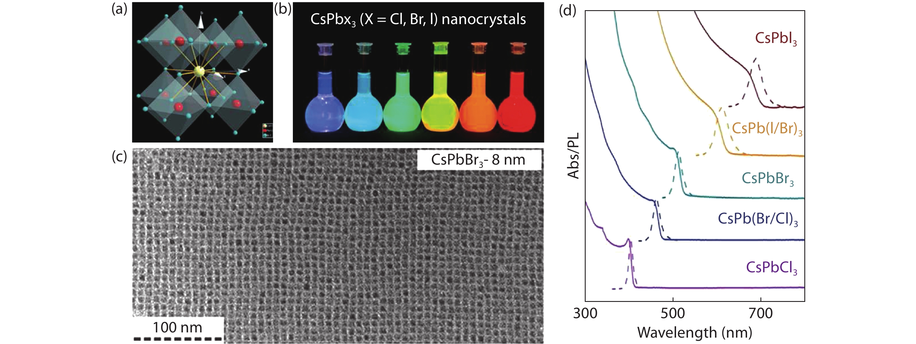
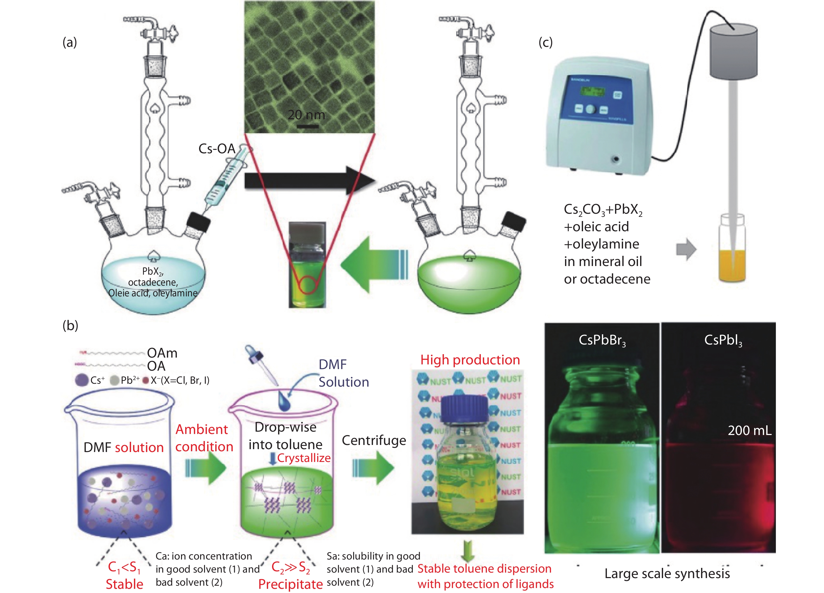
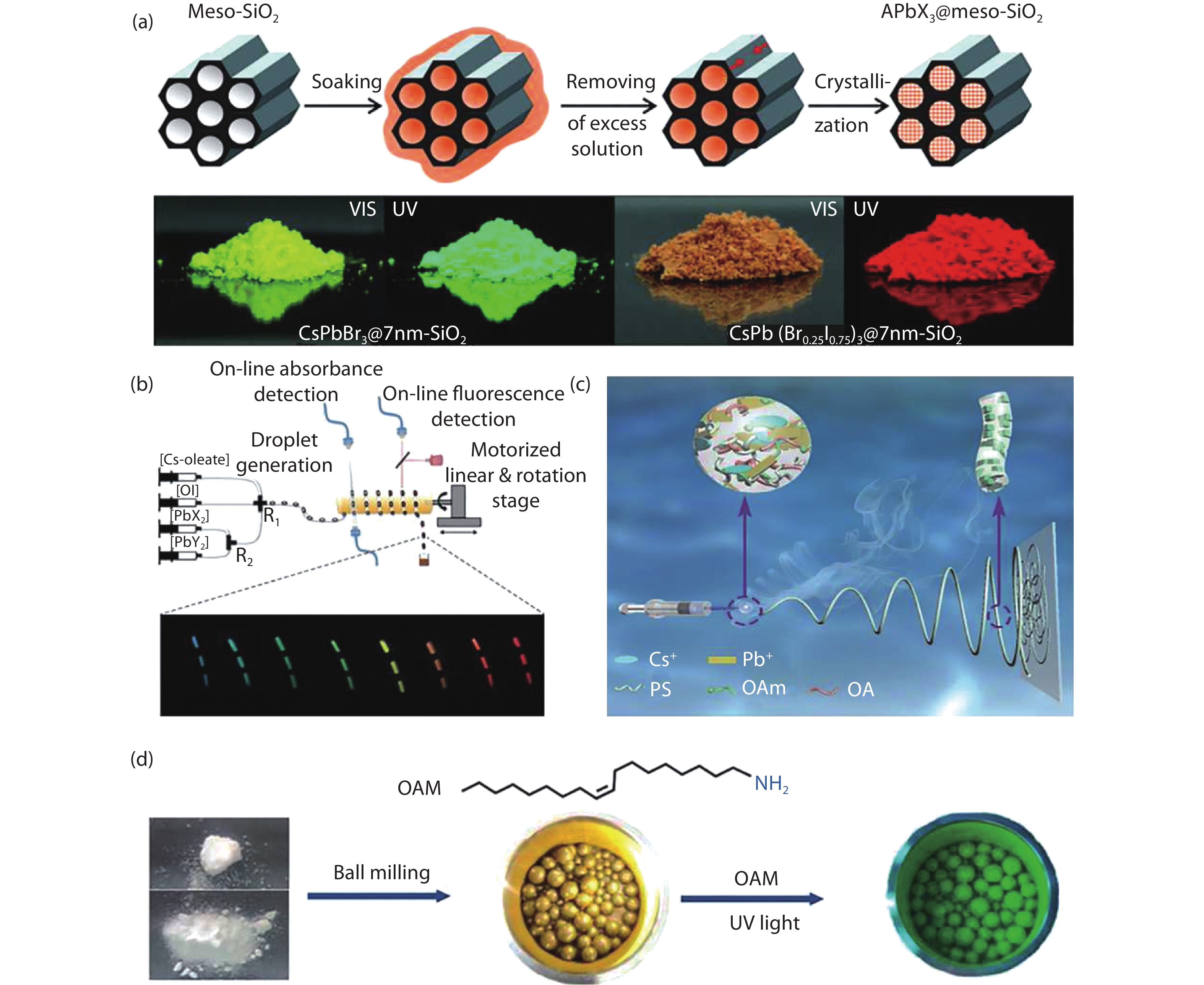
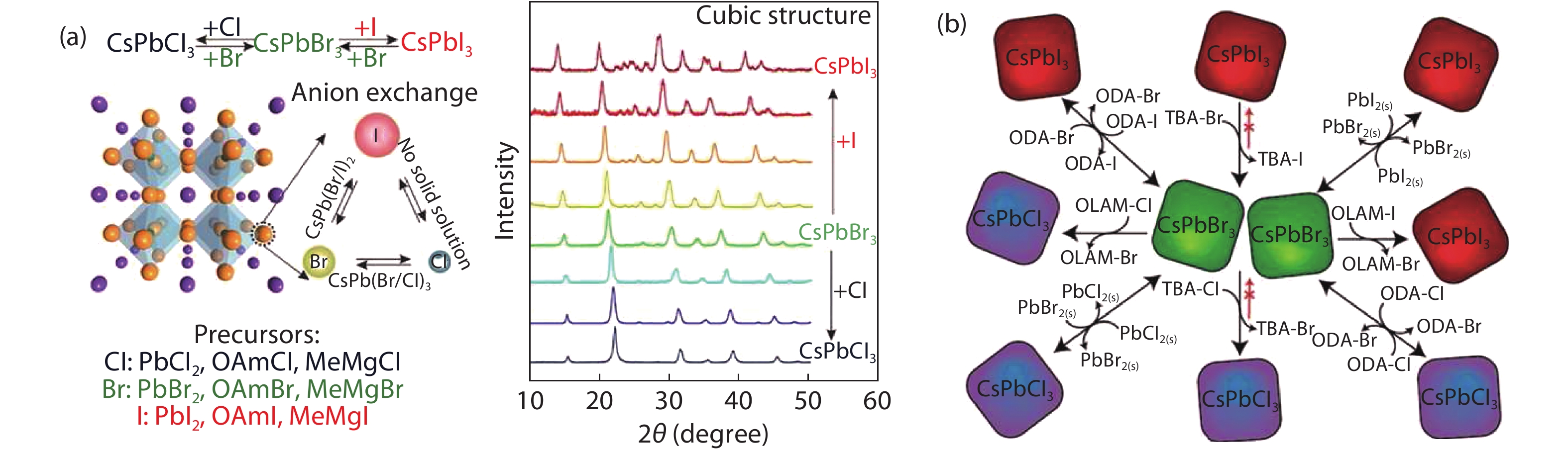
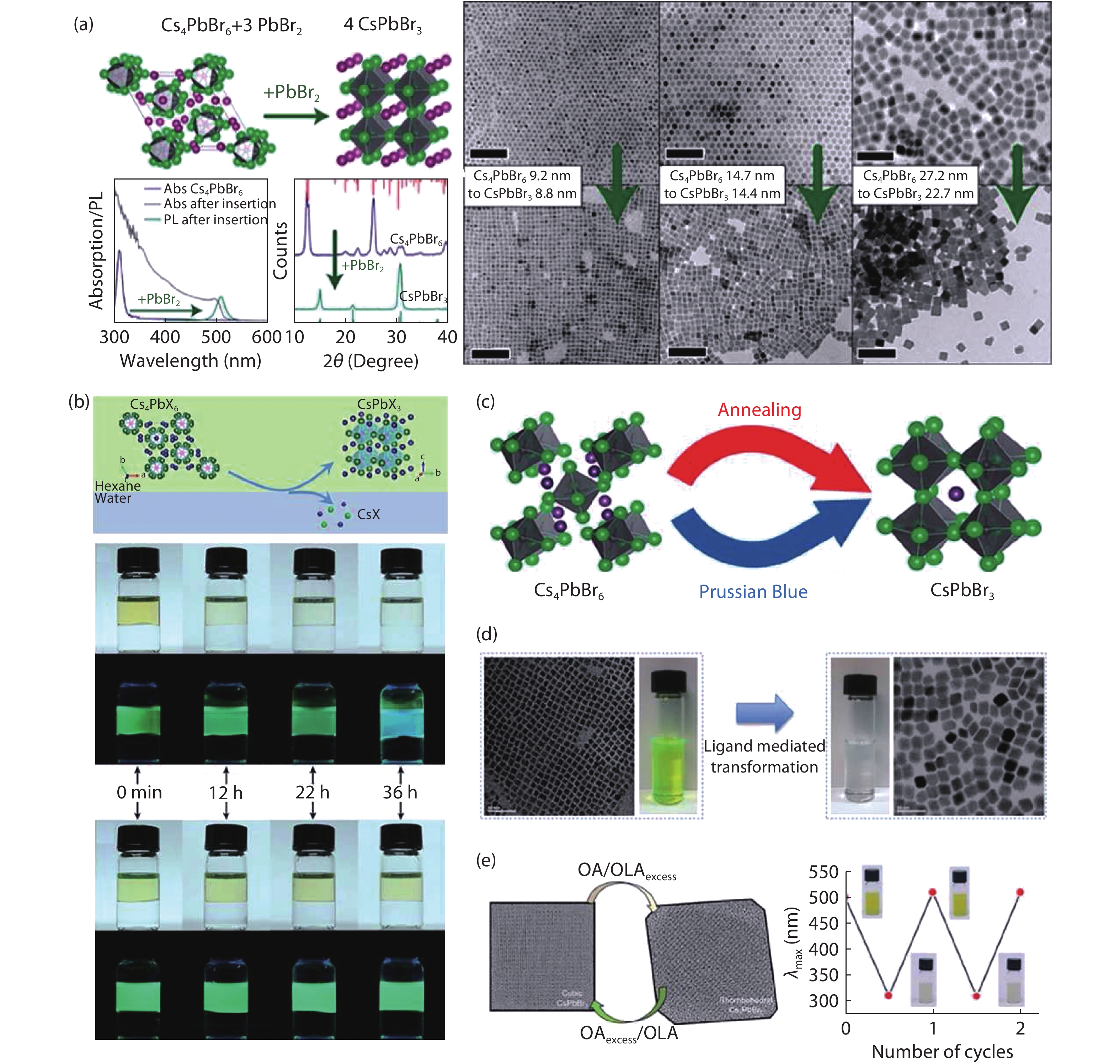
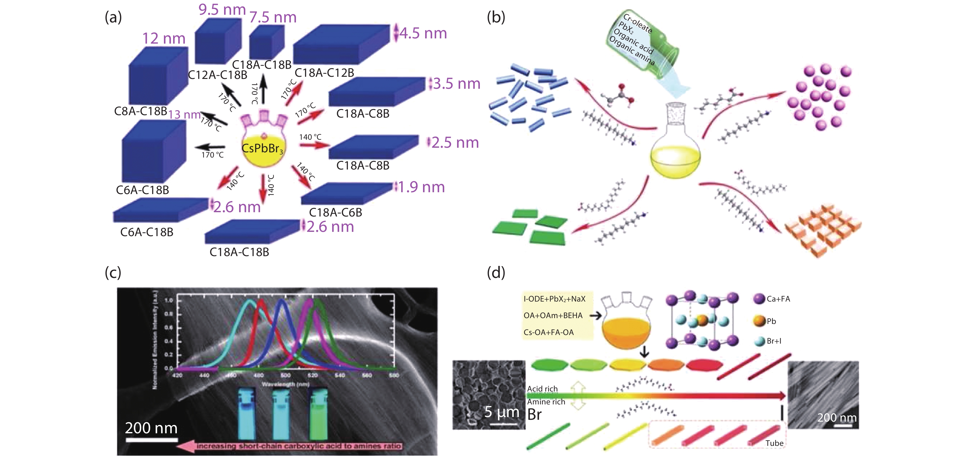
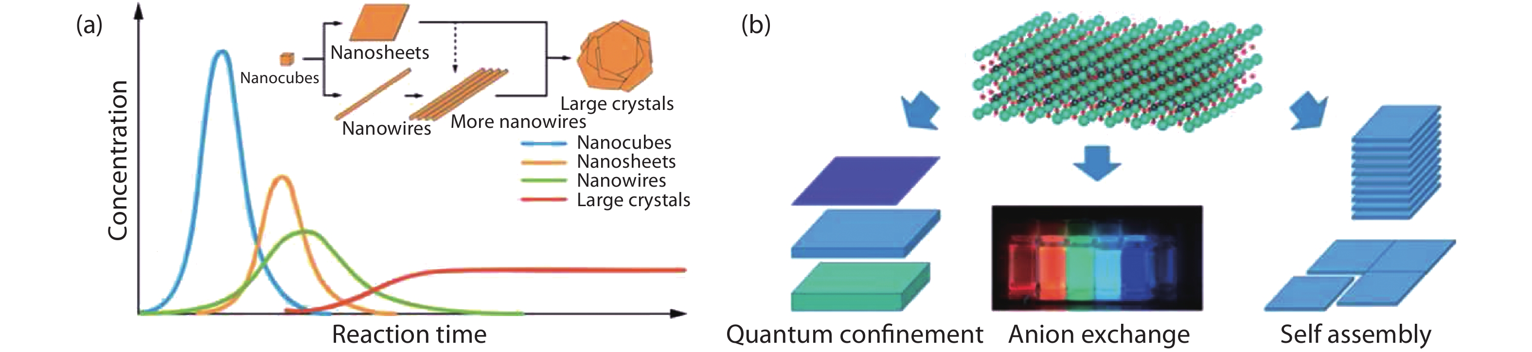
In the past five years, all-inorganic metal halide perovskite (CsPbX3, X = Cl, Br, I) nanocrystals have been intensely studied due to their outstanding optical properties and facile synthesis, which endow them with potential optoelectronic applications. In order to optimize their physical and chemical properties, different strategies have been developed to realize the controllable synthesis of CsPbX3 nanocrystals. In this short review, we firstly present a comprehensive and detailed summary of existed synthesis strategies of CsPbX3 nanocrystals and their analogues. Then, we introduce the regulations of several reaction parameters and their effects on the morphologies of CsPbX3 nanocrystals. At the same time, we provide stability improvement methods and representative applications. Finally, we propose the current challenges and future perspectives of the promising materials.


J. Semicond.
2020, 41(1): 011301 doi: 10.1088/1674-4926/41/1/011301
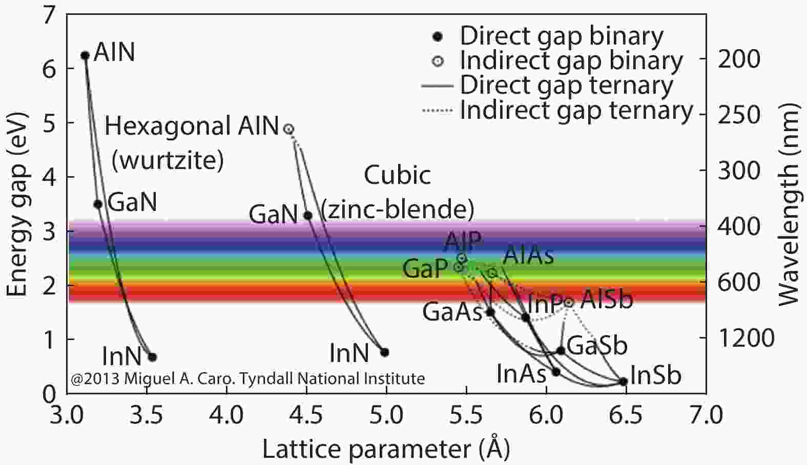
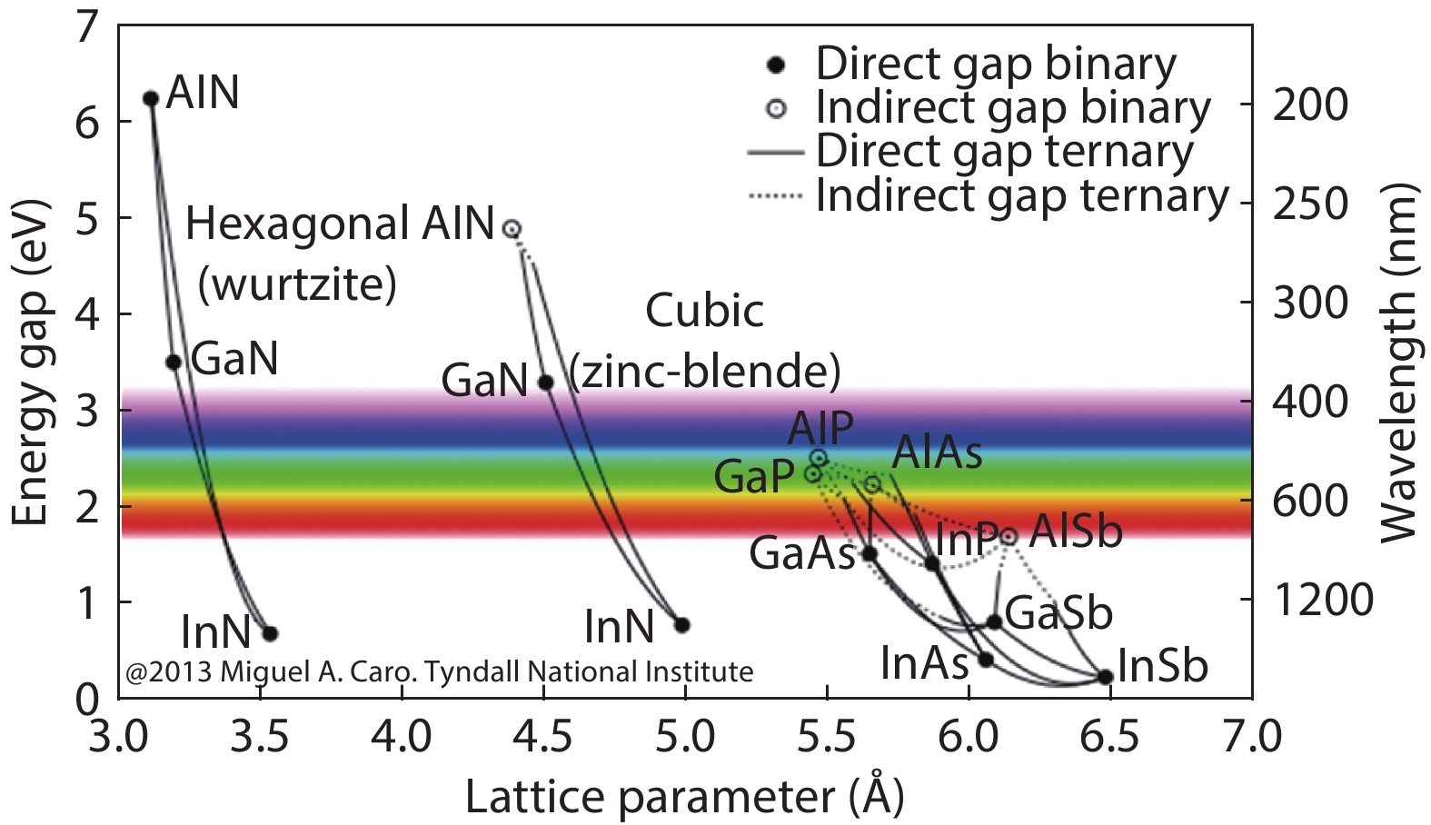
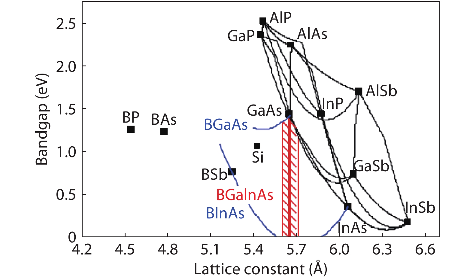
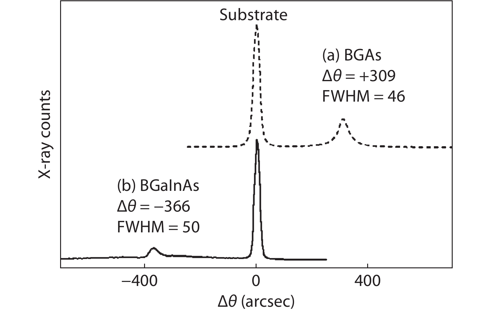
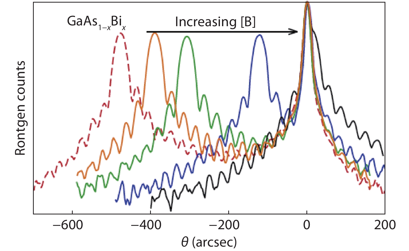
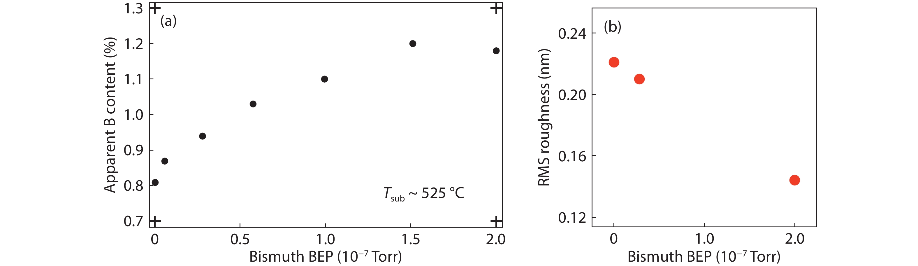
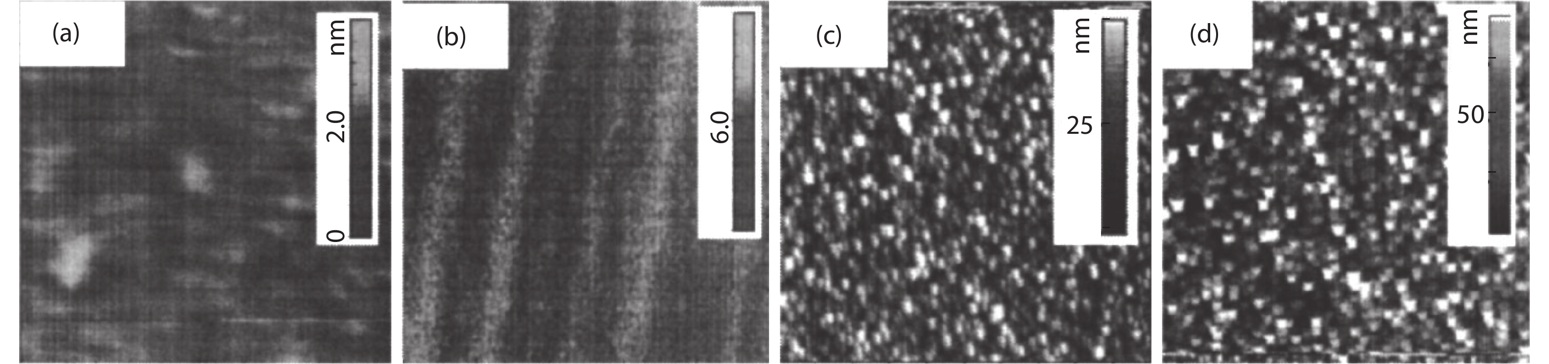
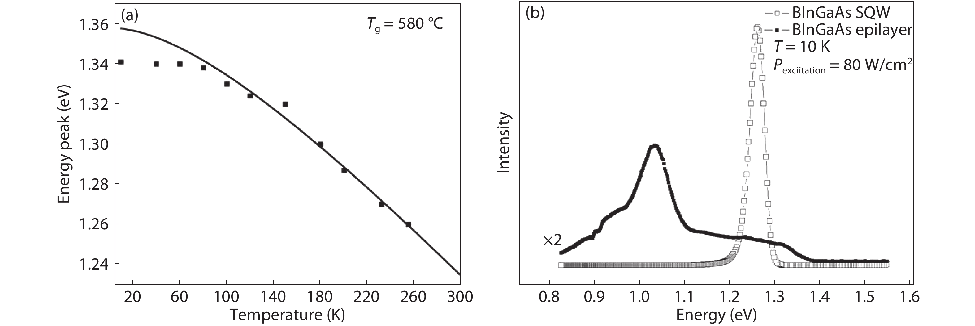
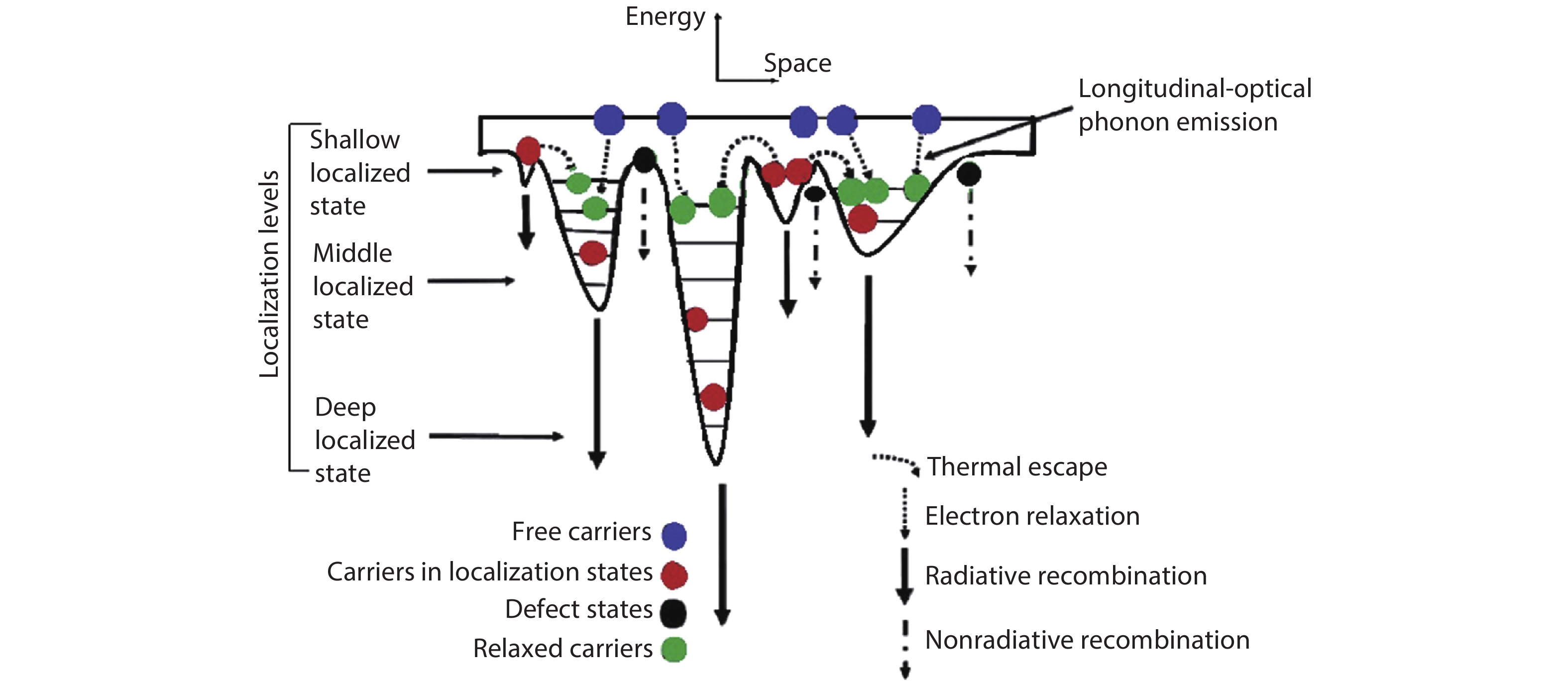
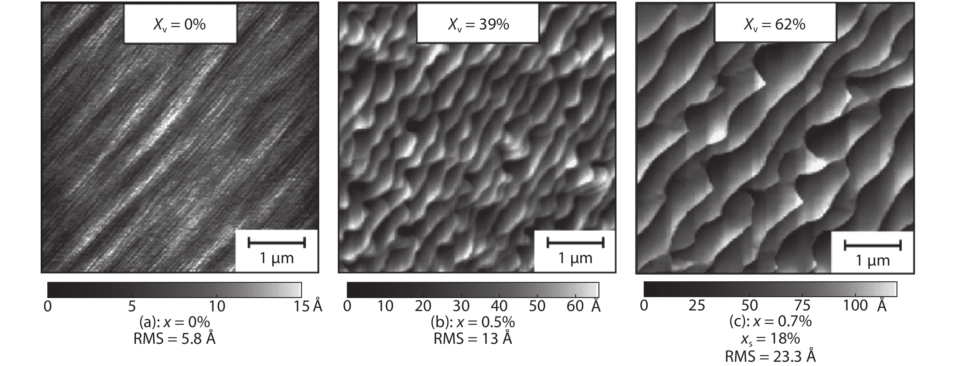
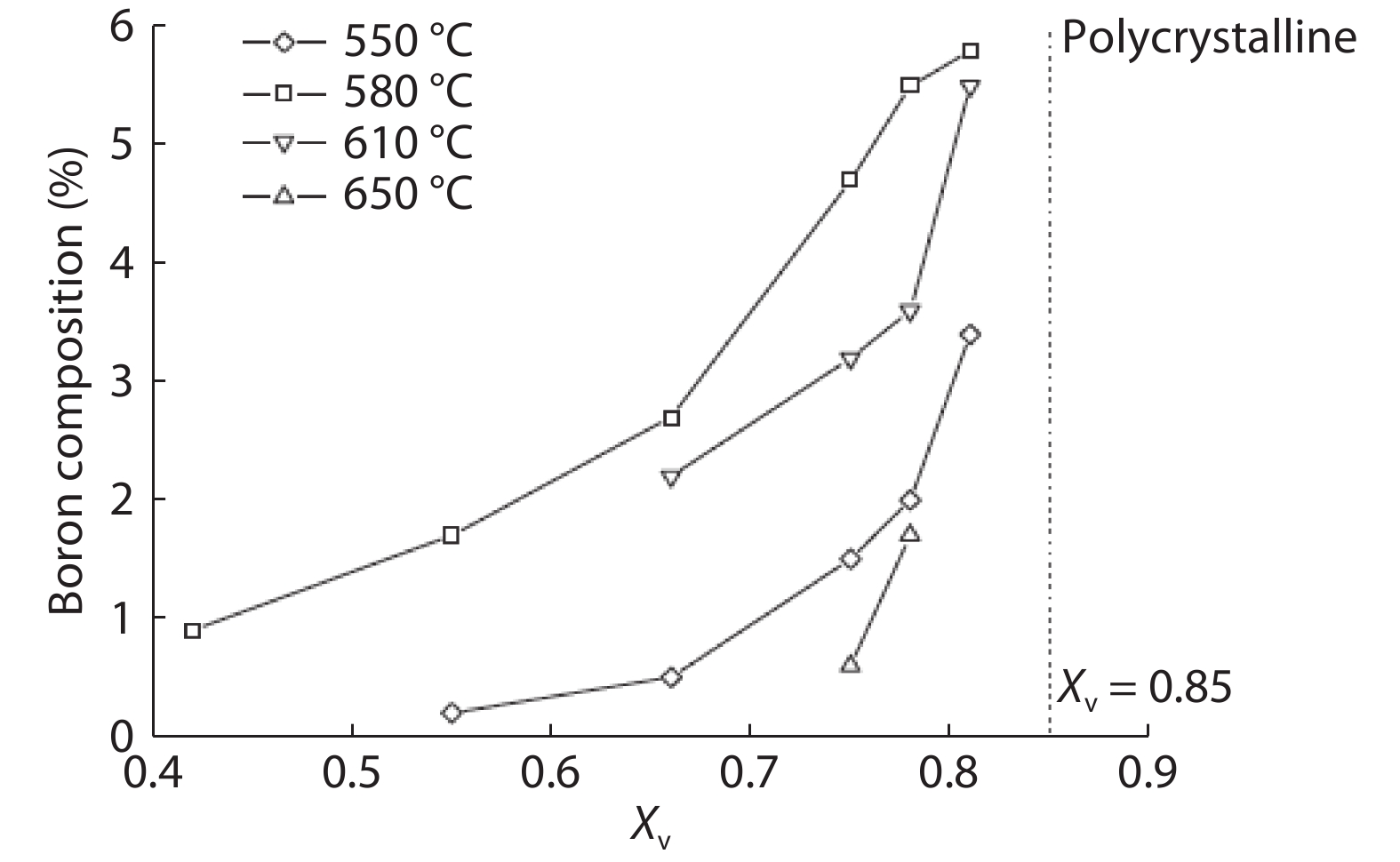
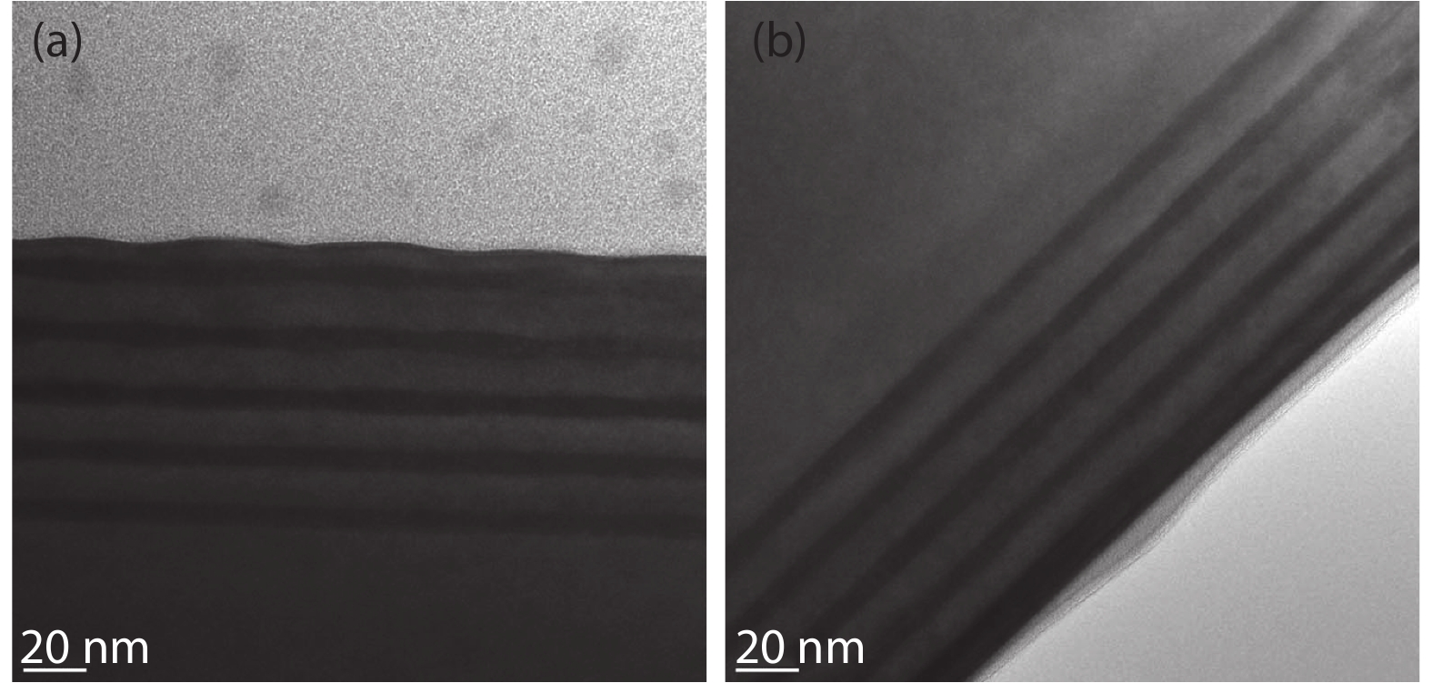
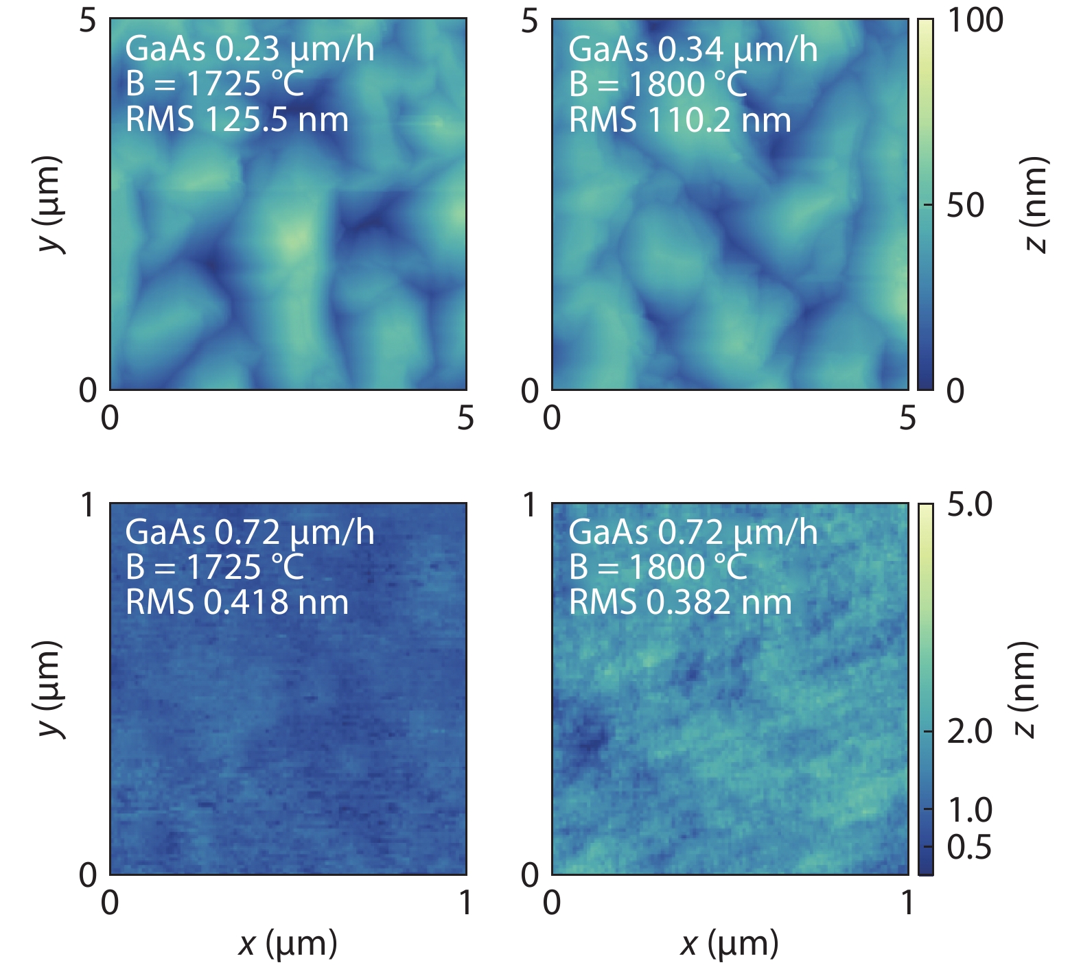
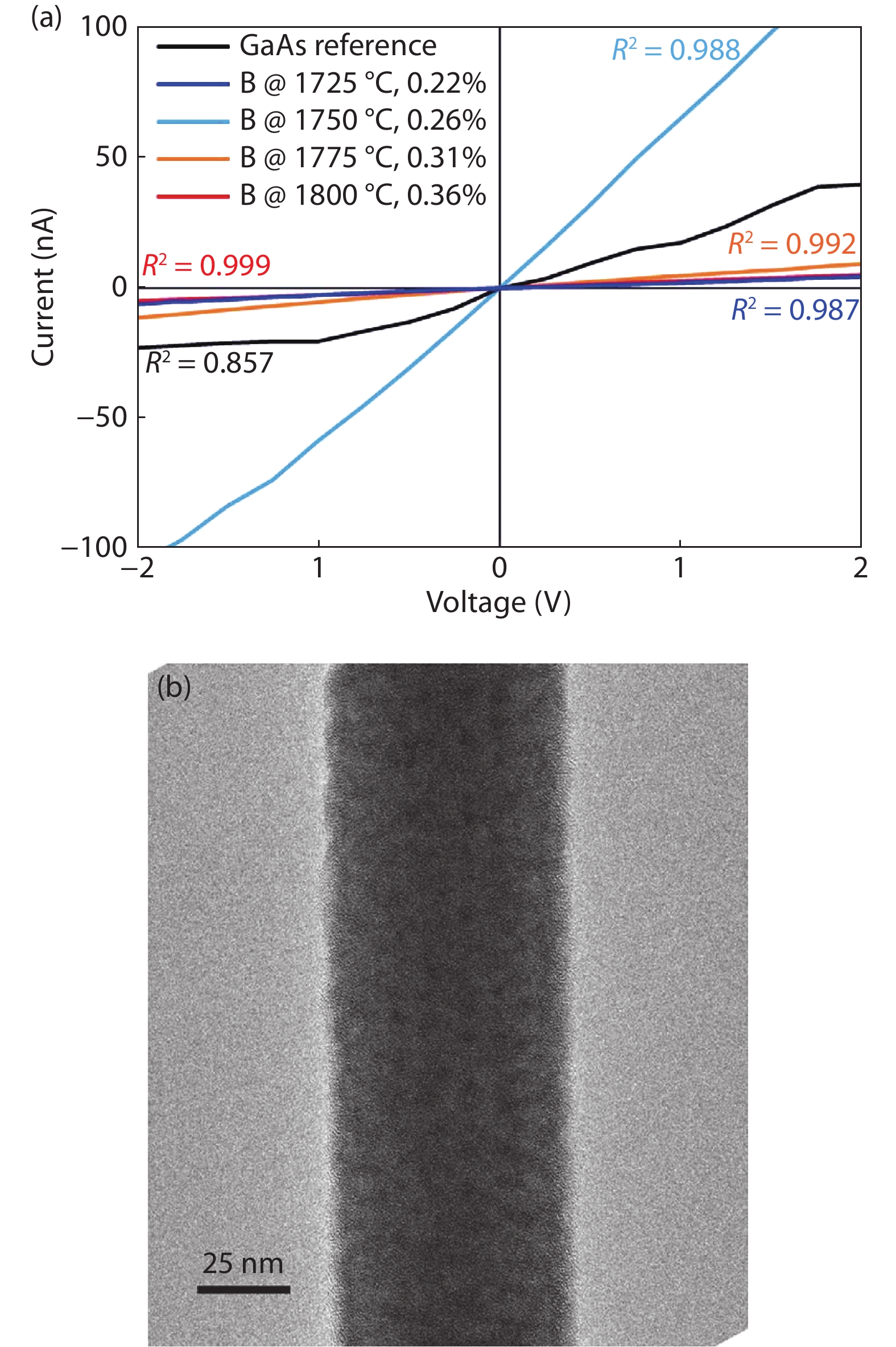
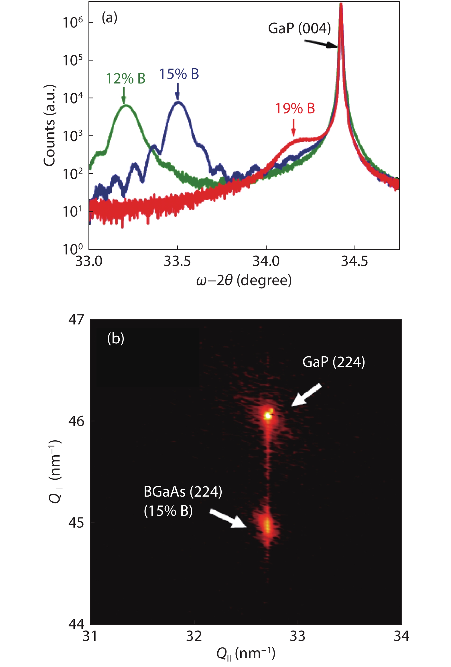
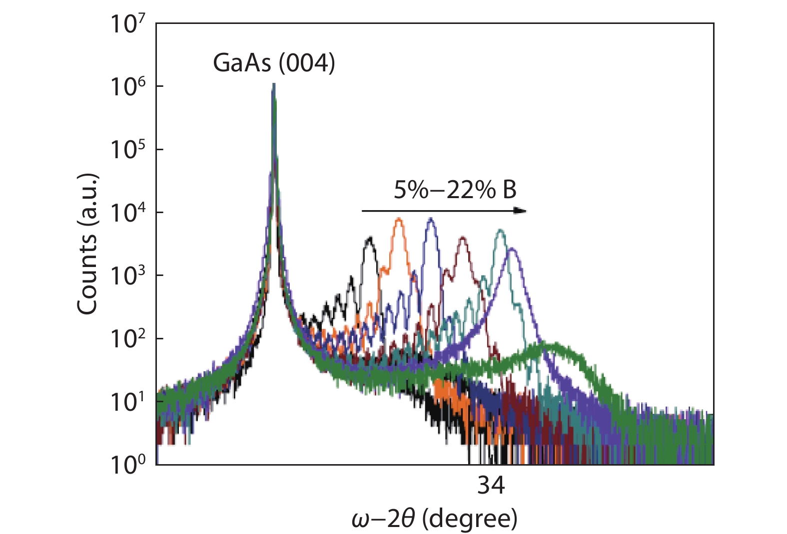
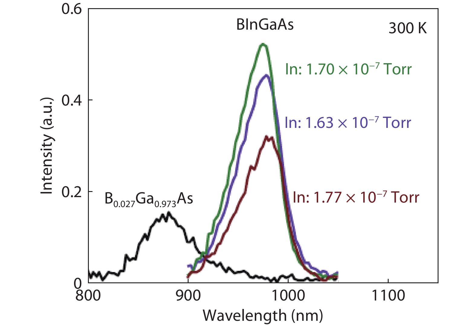
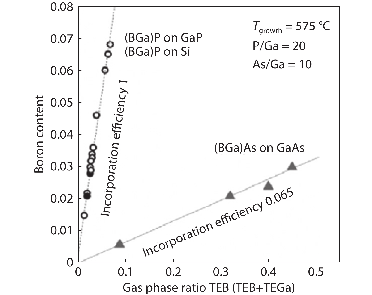
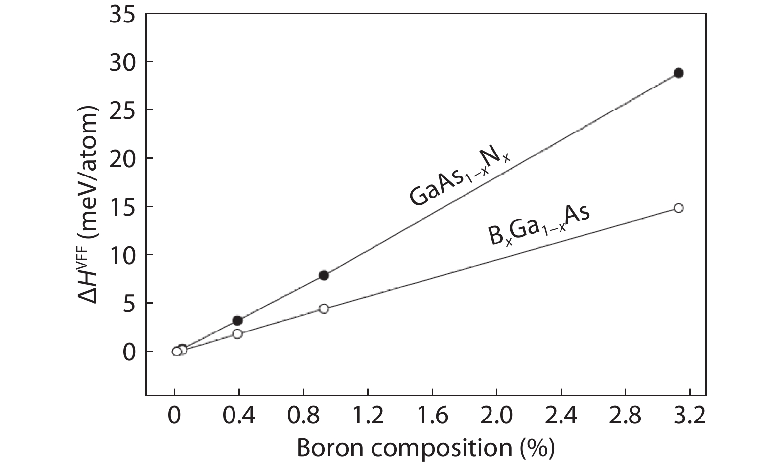
Optoelectronic devices on silicon substrates are essential not only to the optoelectronic integrated circuit but also to low-cost lasers, large-area detectors, and so forth. Although heterogeneous integration of III–V semiconductors on Si has been well-developed, the thermal dissipation issue and the complicated fabrication process still hinders the development of these devices. The monolithic growth of III–V materials on Si has also been demonstrated by applying complicated buffer layers or interlayers. On the other hand, the growth of lattice-matched B-doped group-III–V materials is an attractive area of research. However, due to the difficulty in growth, the development is still relatively slow. Herein, we present a comprehensive review of the recent achievements in this field. We summarize and discuss the conditions and mechanisms involved in growing B-doped group-III–V materials. The unique surface morphology, crystallinity, and optical properties of the epitaxy correlating with their growth conditions are discussed, along with their respective optoelectronic applications. Finally, we detail the obstacles and challenges to exploit the potential for such practical applications fully.

J. Semicond.
2020, 41(1): 011701 doi: 10.1088/1674-4926/41/1/011701
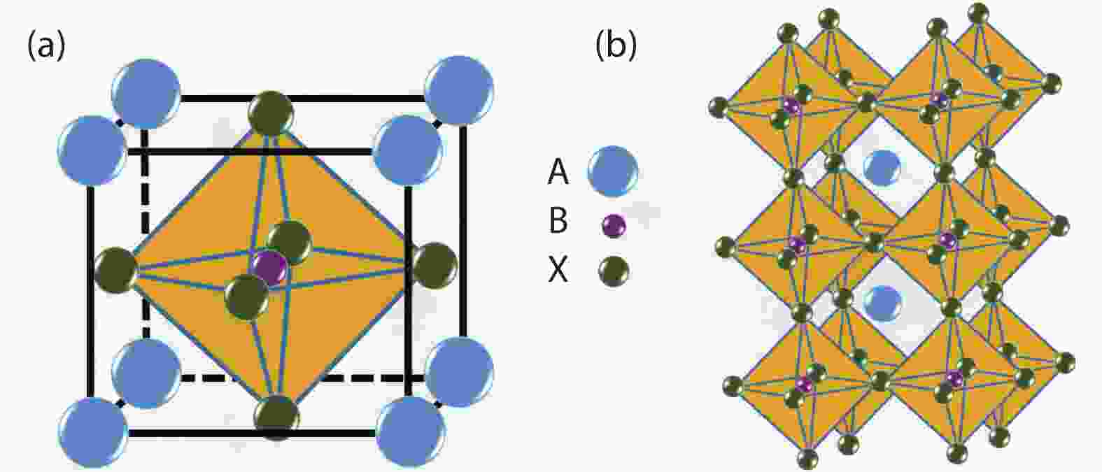
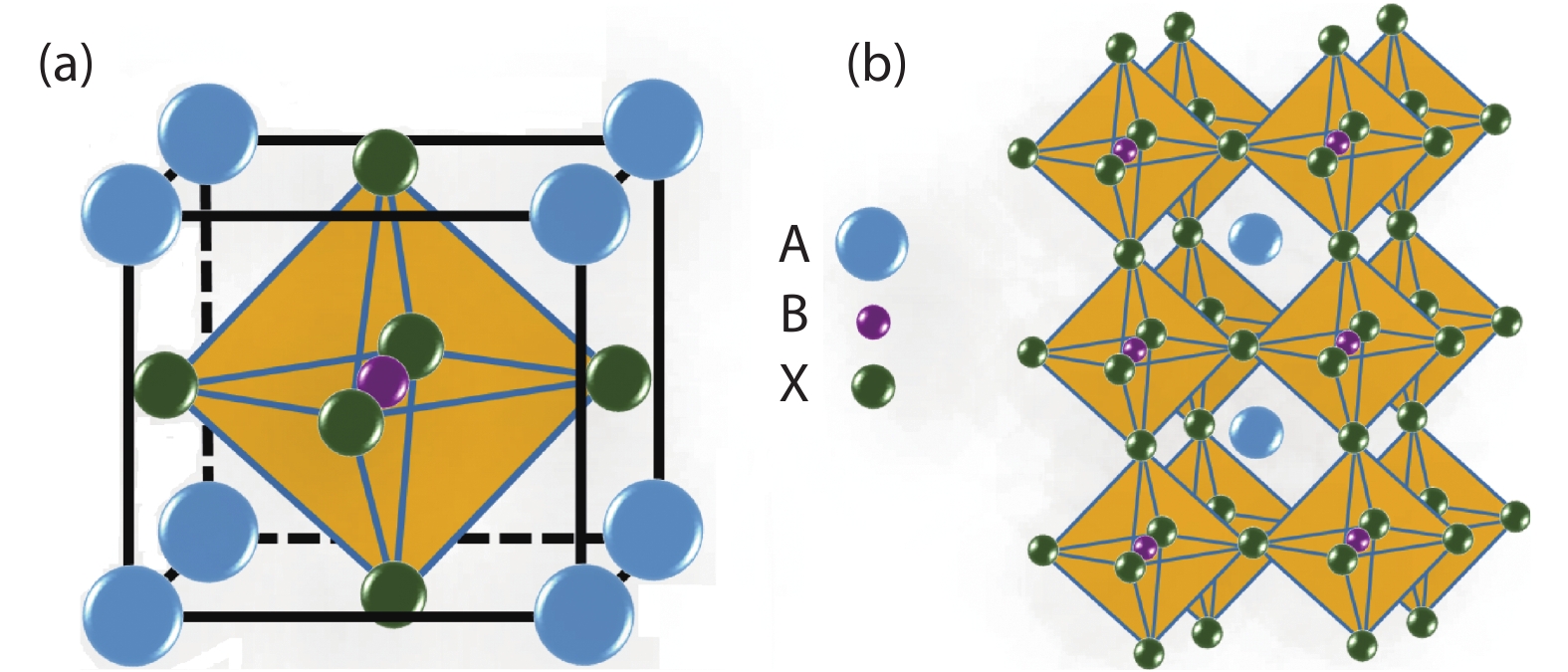
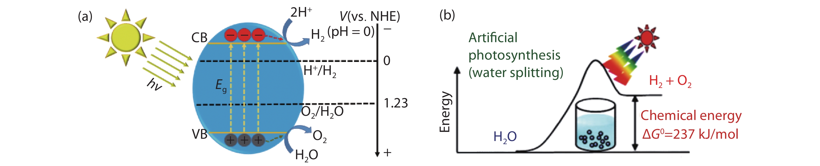
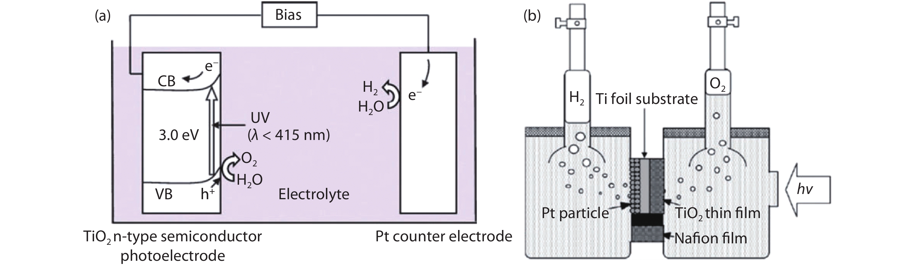
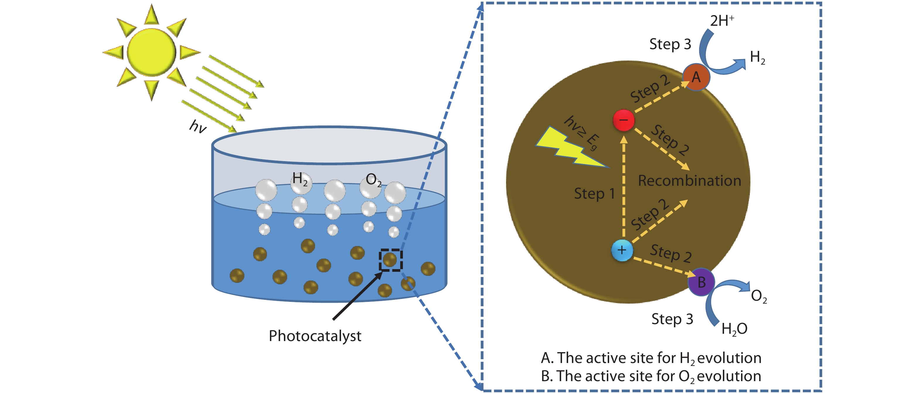
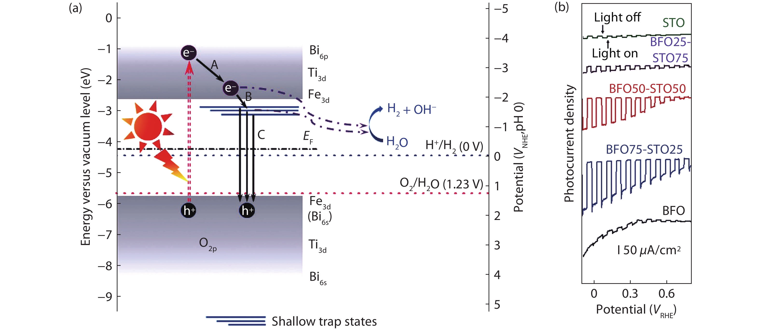
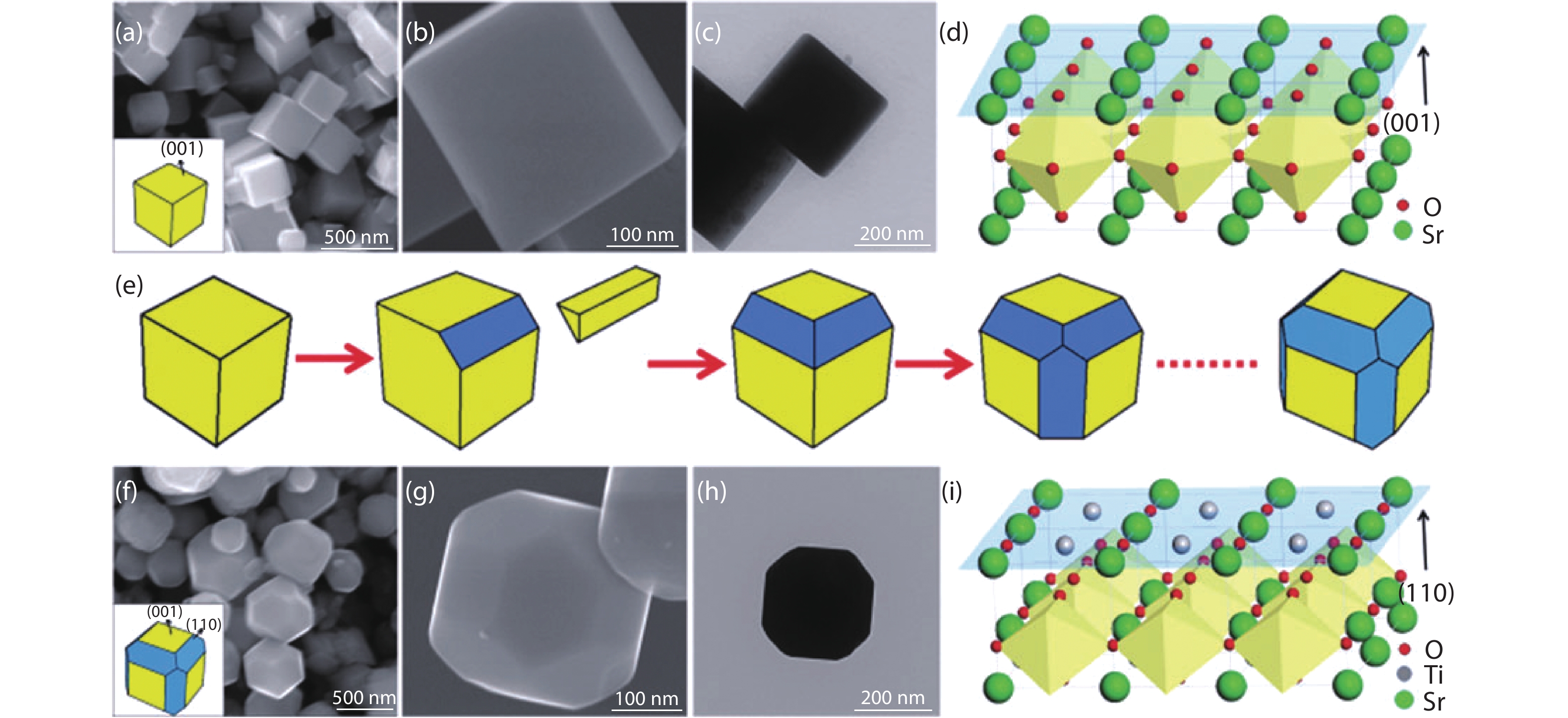
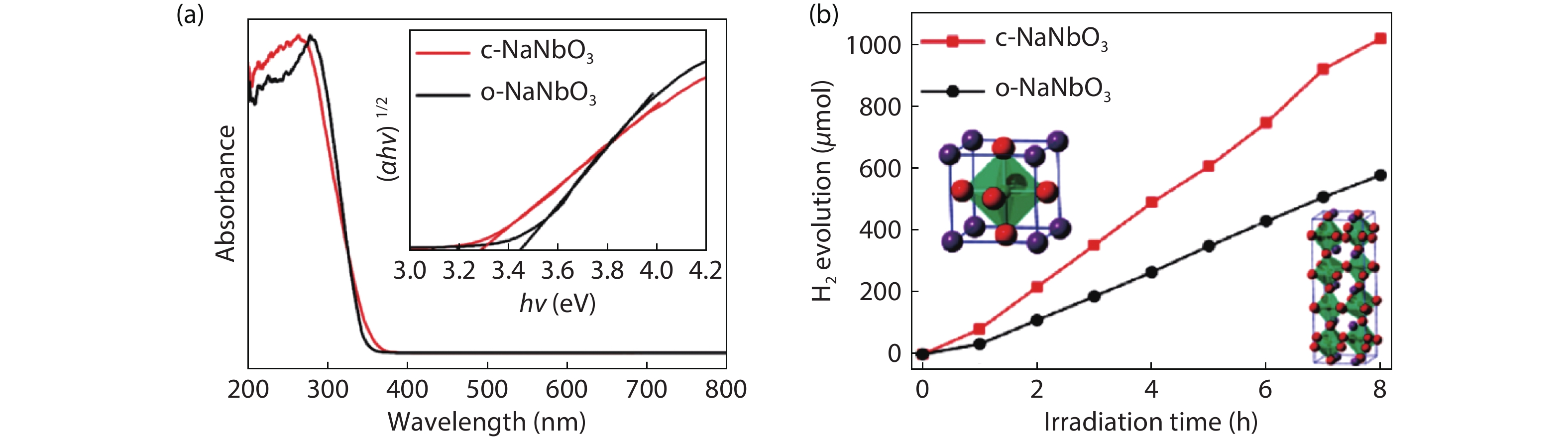
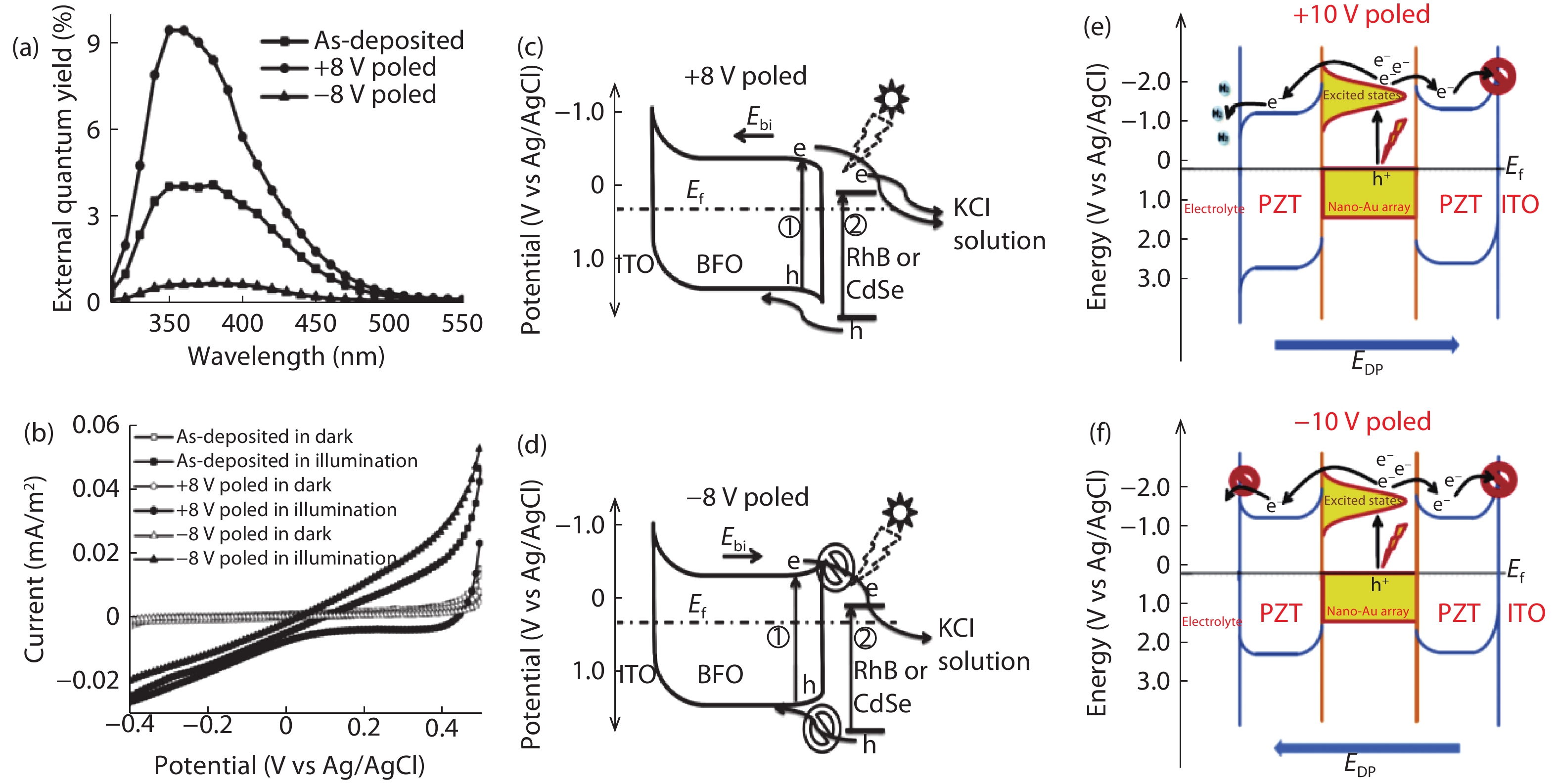
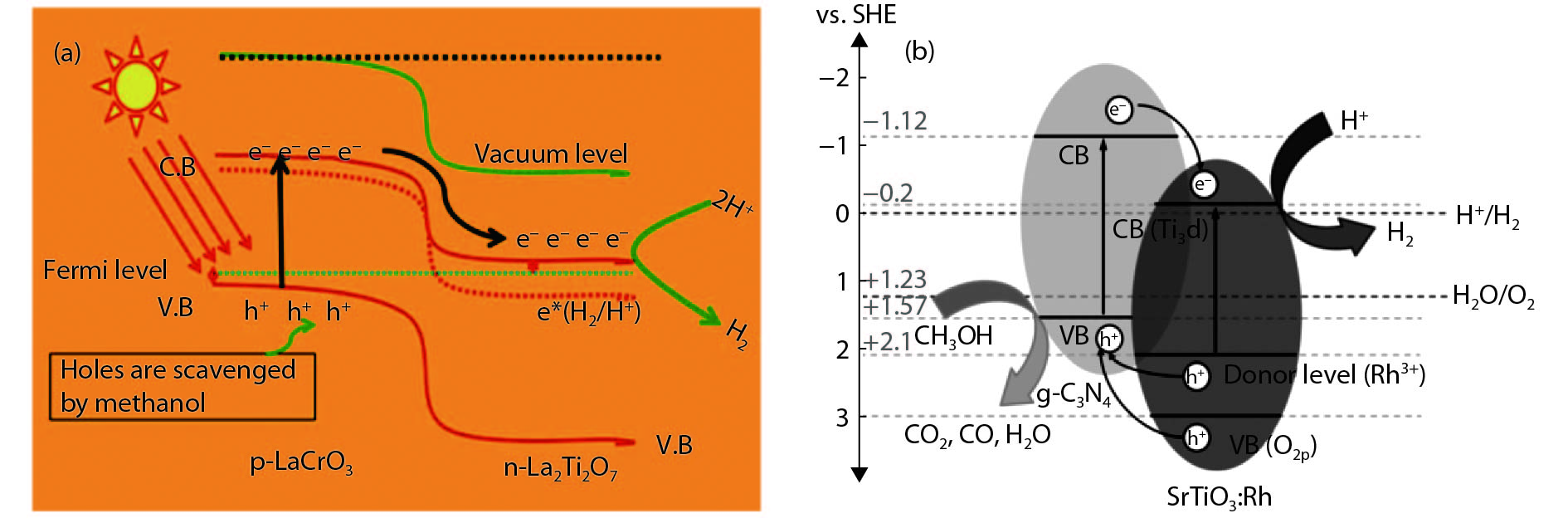
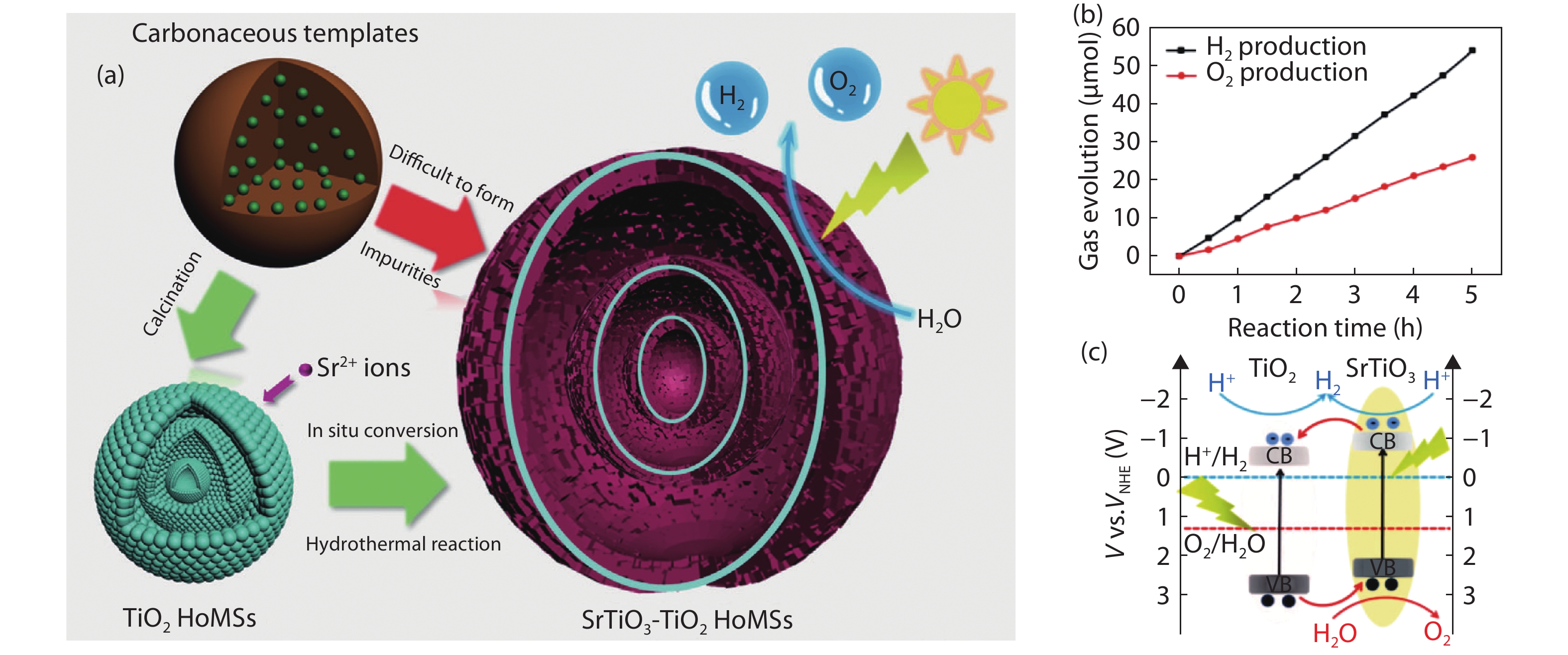
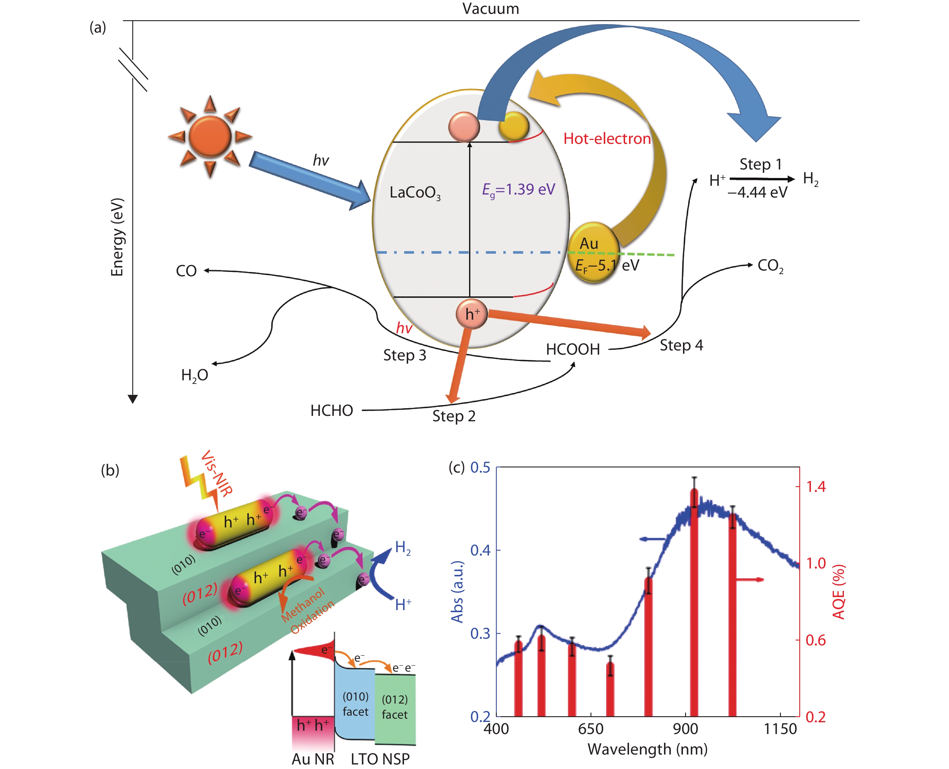
Solar water splitting is a promising strategy for sustainable production of renewable hydrogen, and solving the crisis of energy and environment in the world. However, large-scale application of this method is hampered by the efficiency and the expense of the solar water splitting systems. Searching for non-toxic, low-cost, efficient and stable photocatalysts is an important way for solar water splitting. Due to the simplicity of structure and the flexibility of composition, perovskite based photocatalysts have recently attracted widespread attention for application in solar water splitting. In this review, the recent developments of perovskite based photocatalysts for water splitting are summarized. An introduction including the structures and properties of perovskite materials, and the fundamentals of solar water splitting is first provided. Then, it specifically focuses on the strategies for designing and modulating perovskite materials to improve their photocatalytic performance for solar water splitting. The current challenges and perspectives of perovskite materials in solar water splitting are also reviewed. The aim of this review is to summarize recent findings and developments of perovskite based photocatalysts and provide some useful guidance for the future research on the design and development of highly efficient perovskite based photocatalysts and the relevant systems for water splitting.

J. Semicond.
2020, 41(1): 011901 doi: 10.1088/1674-4926/41/1/011901

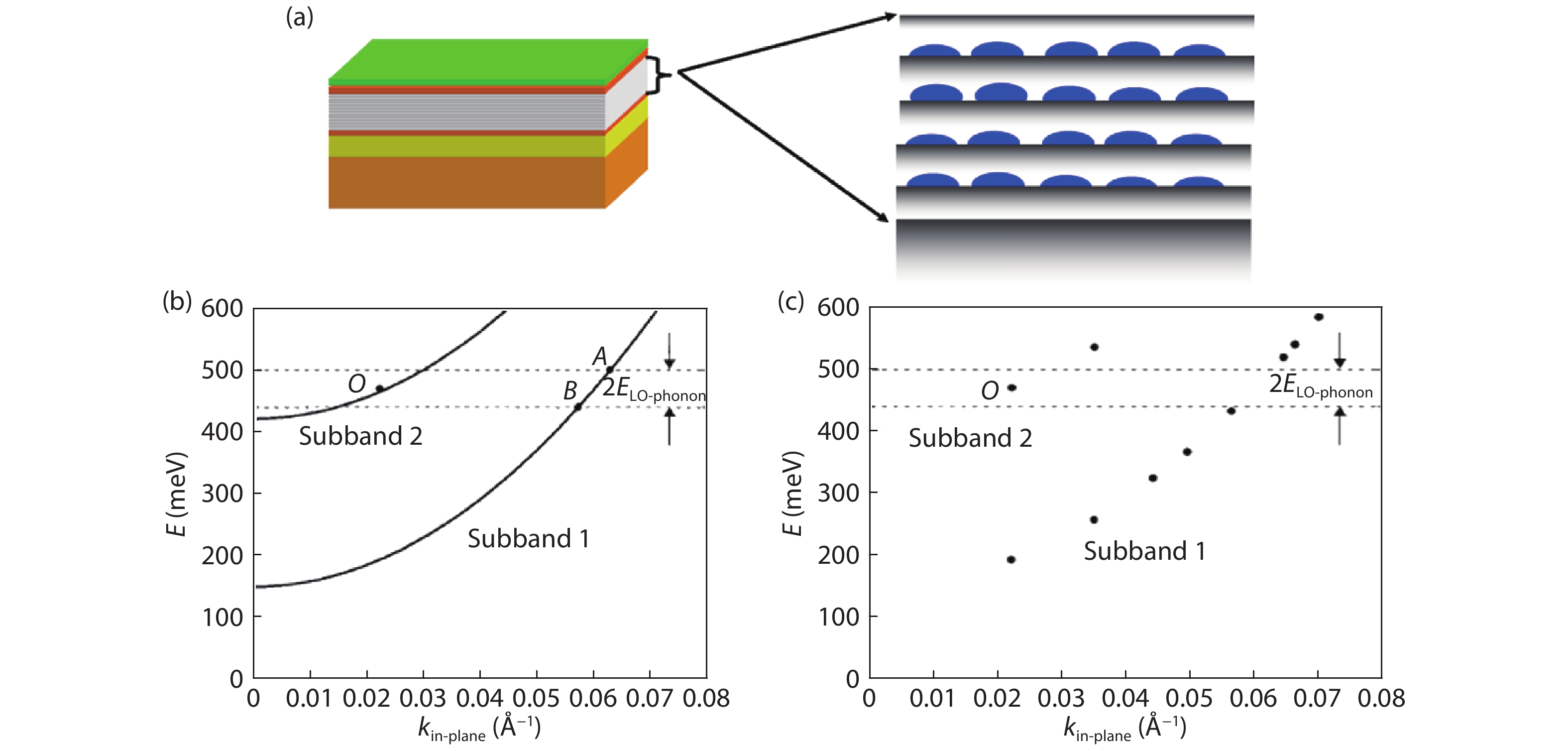
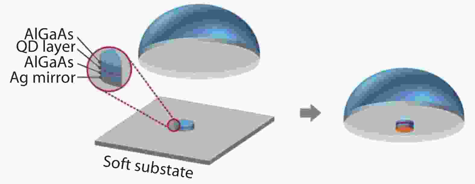
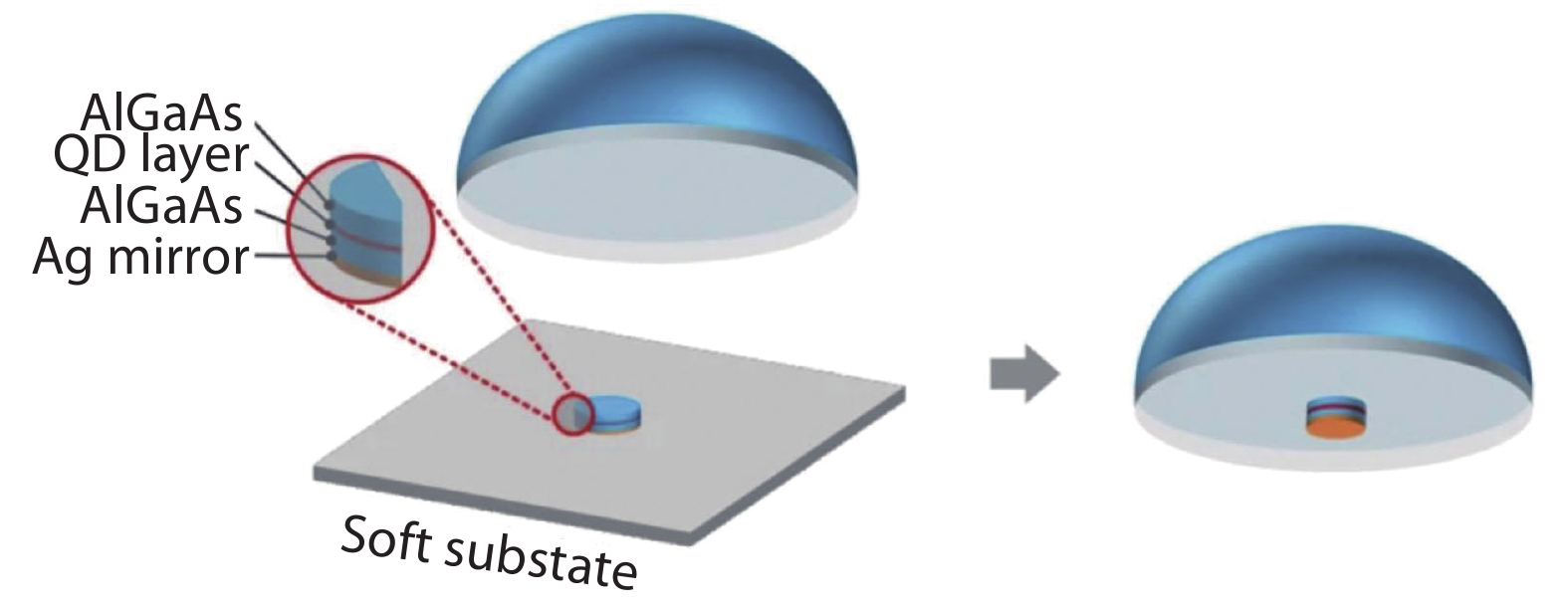
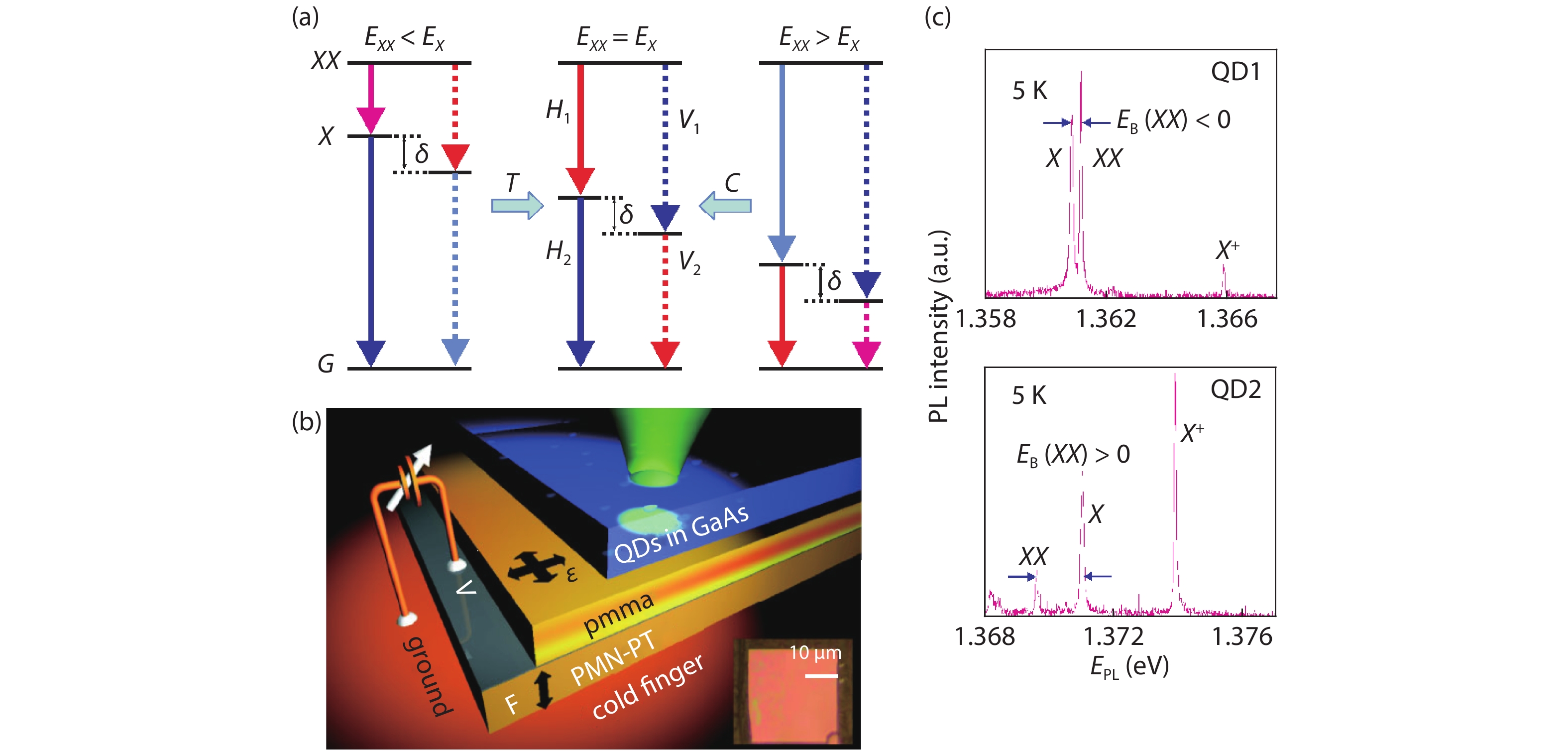
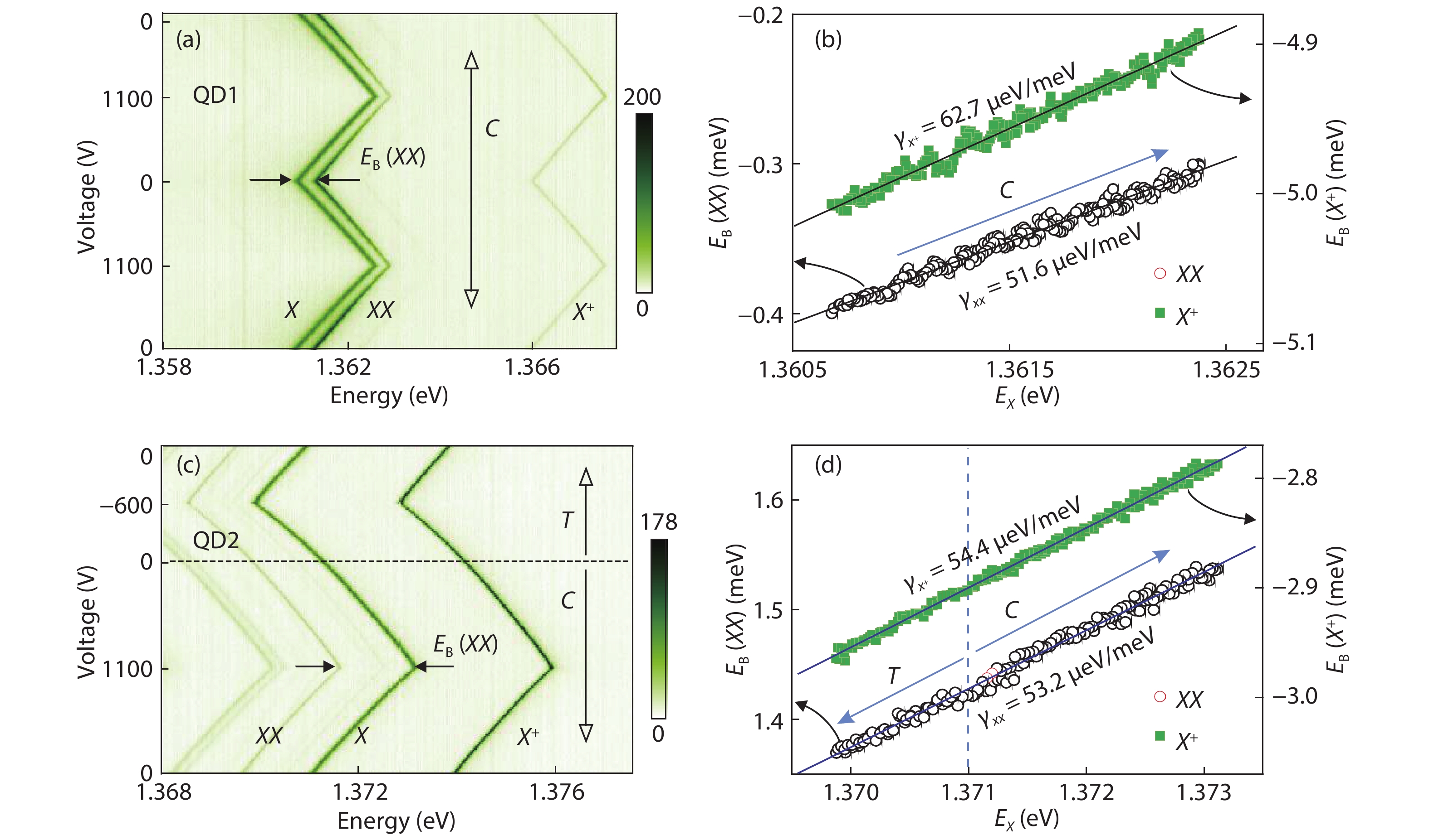
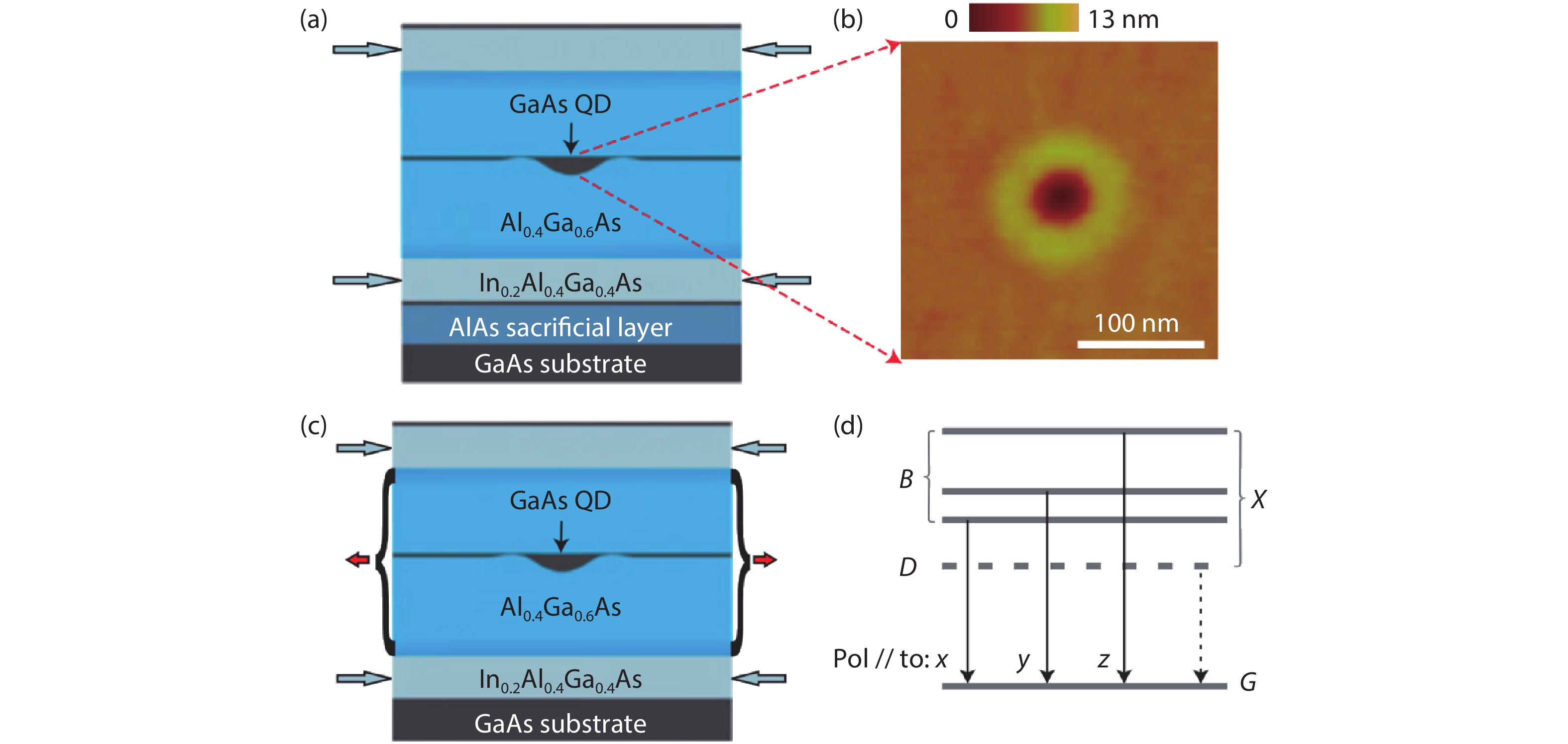
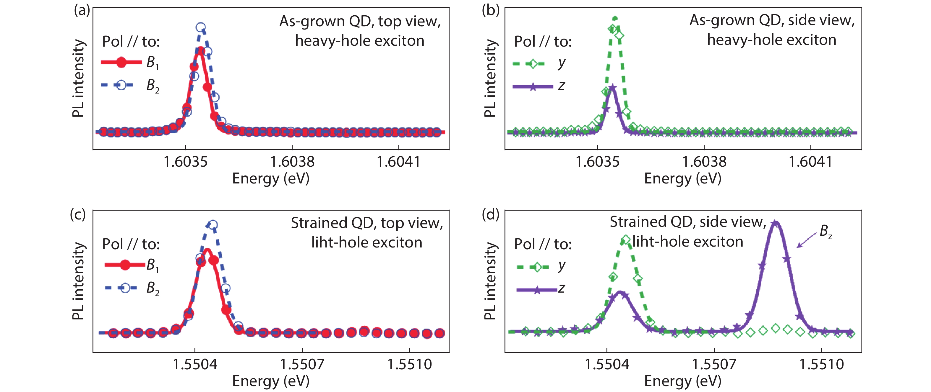
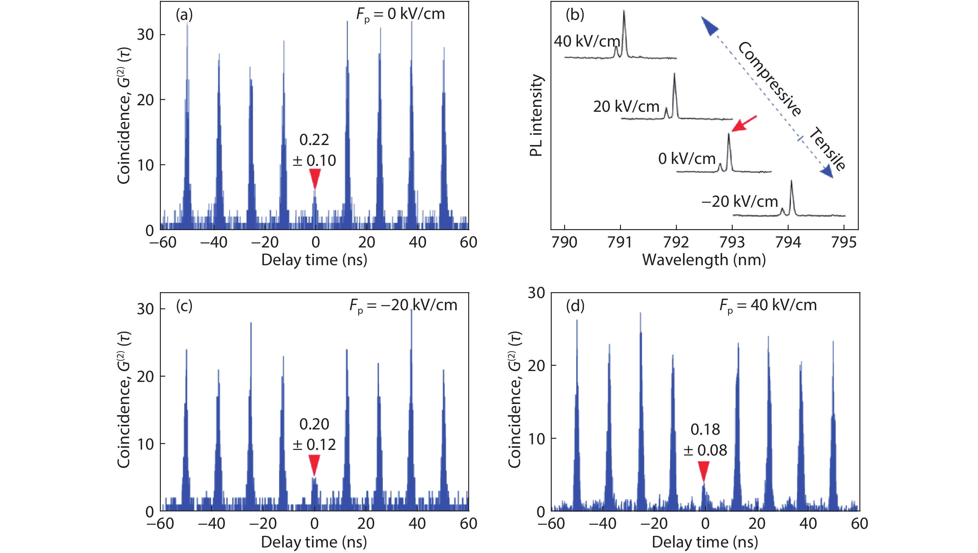
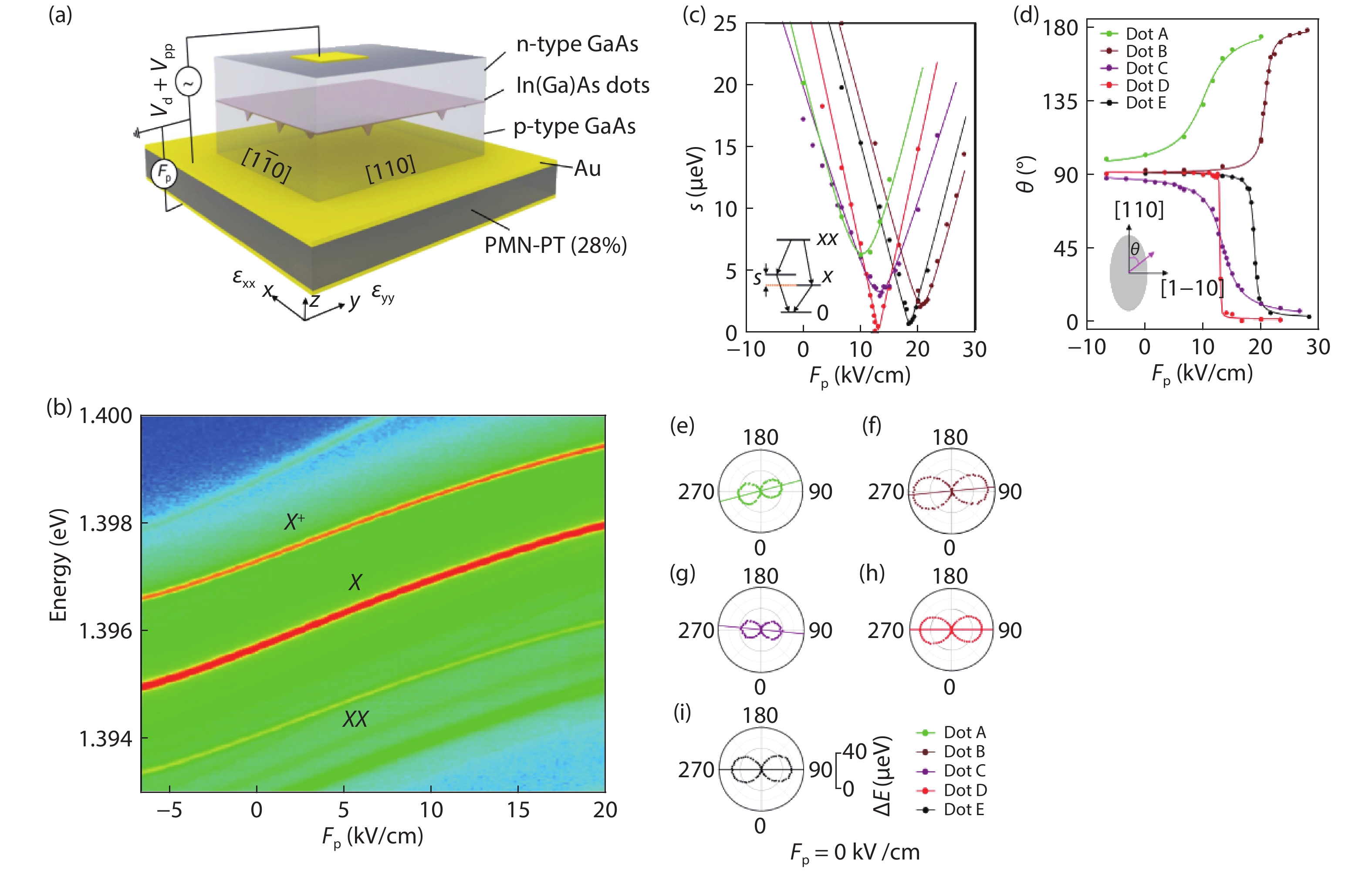
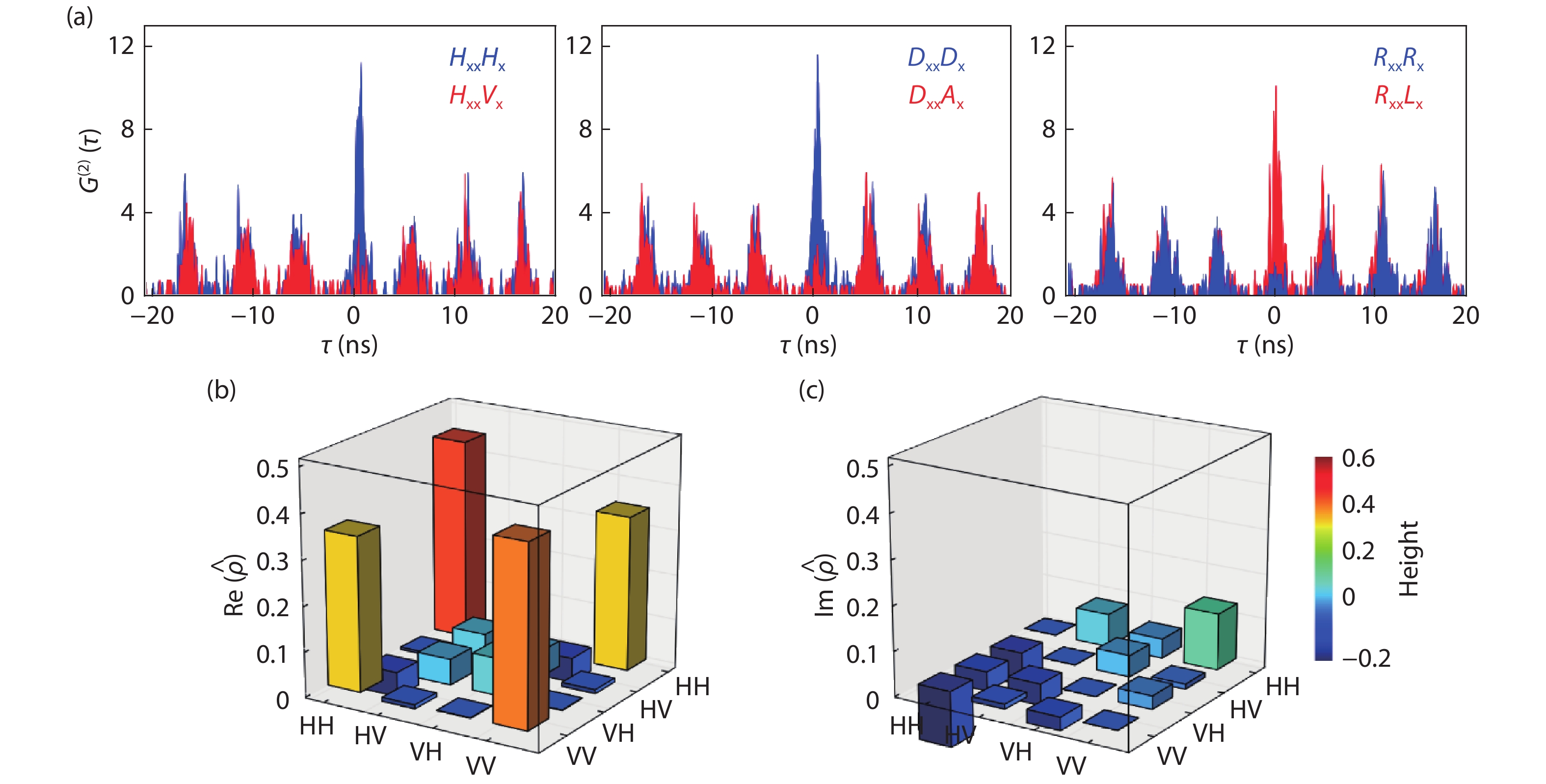
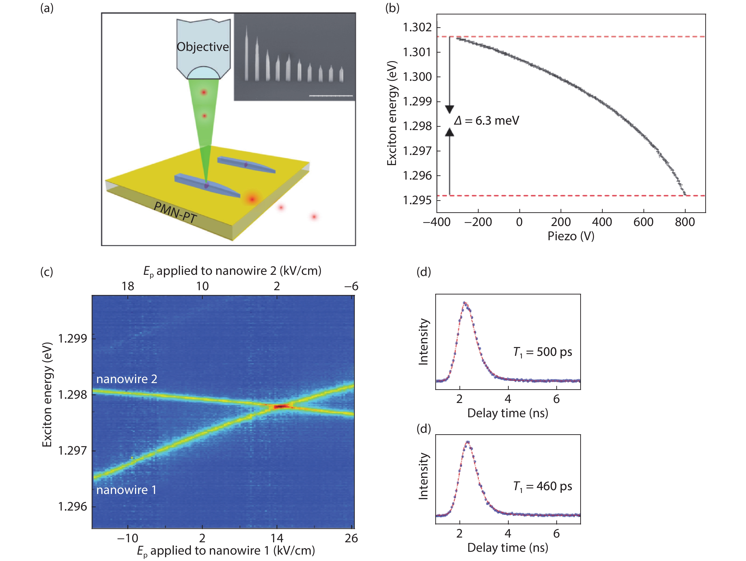
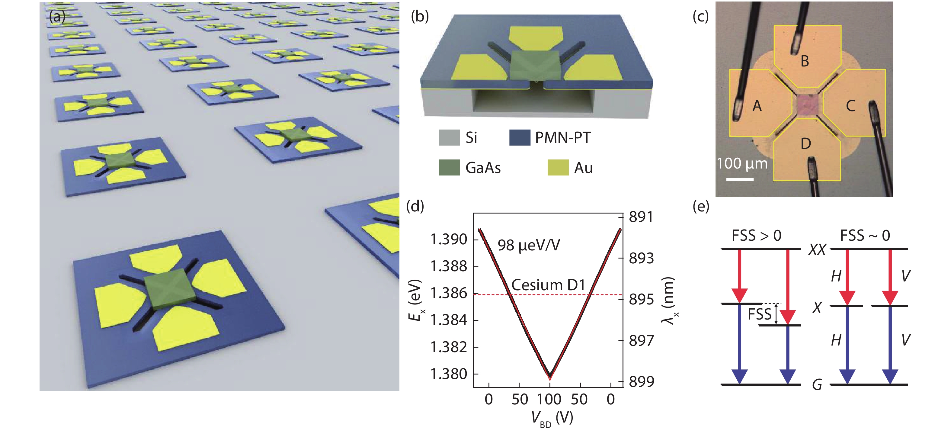
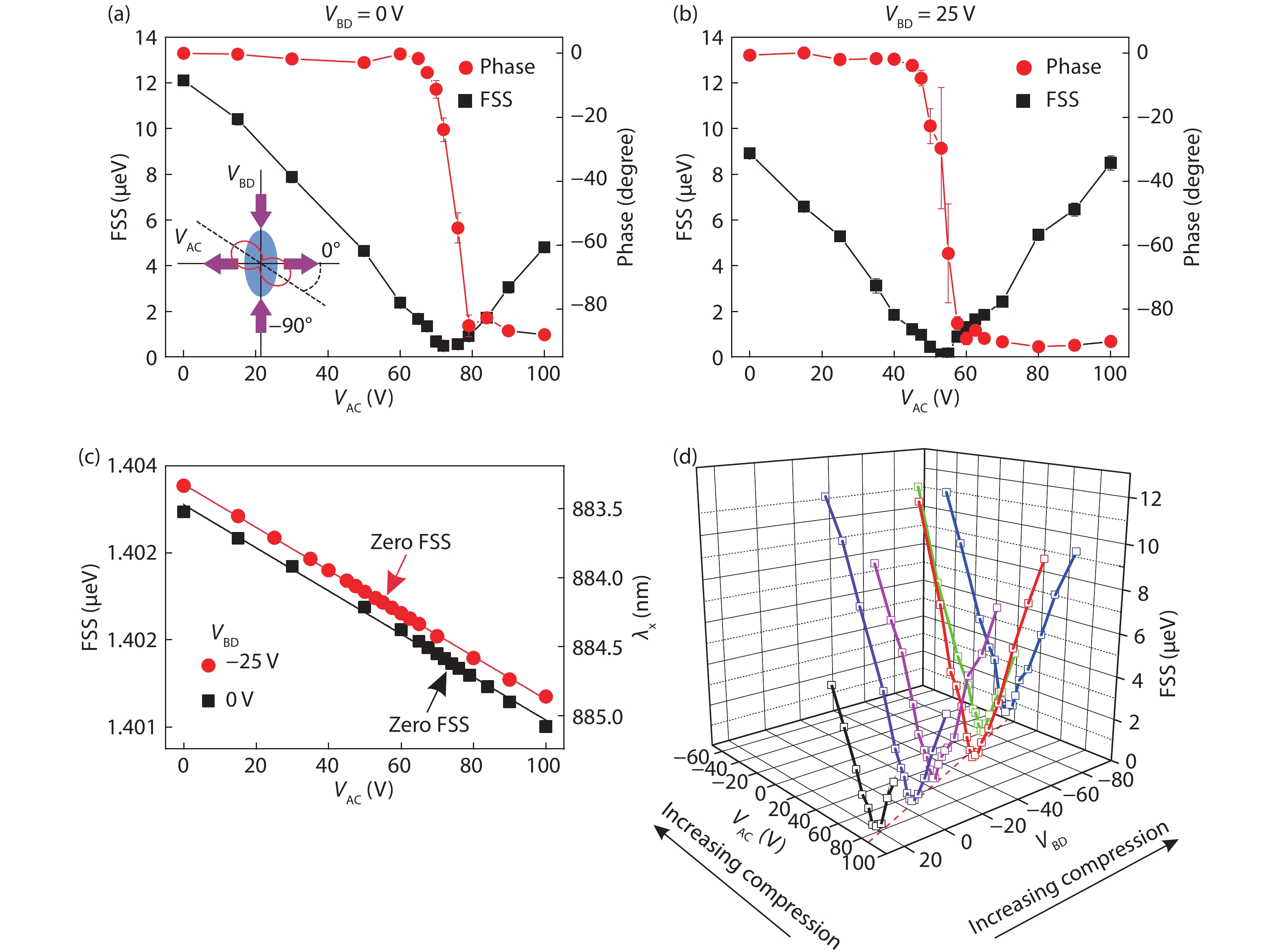
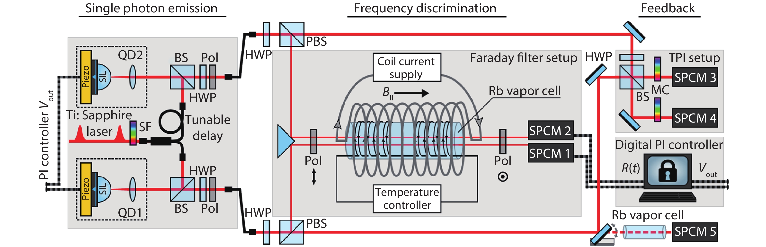
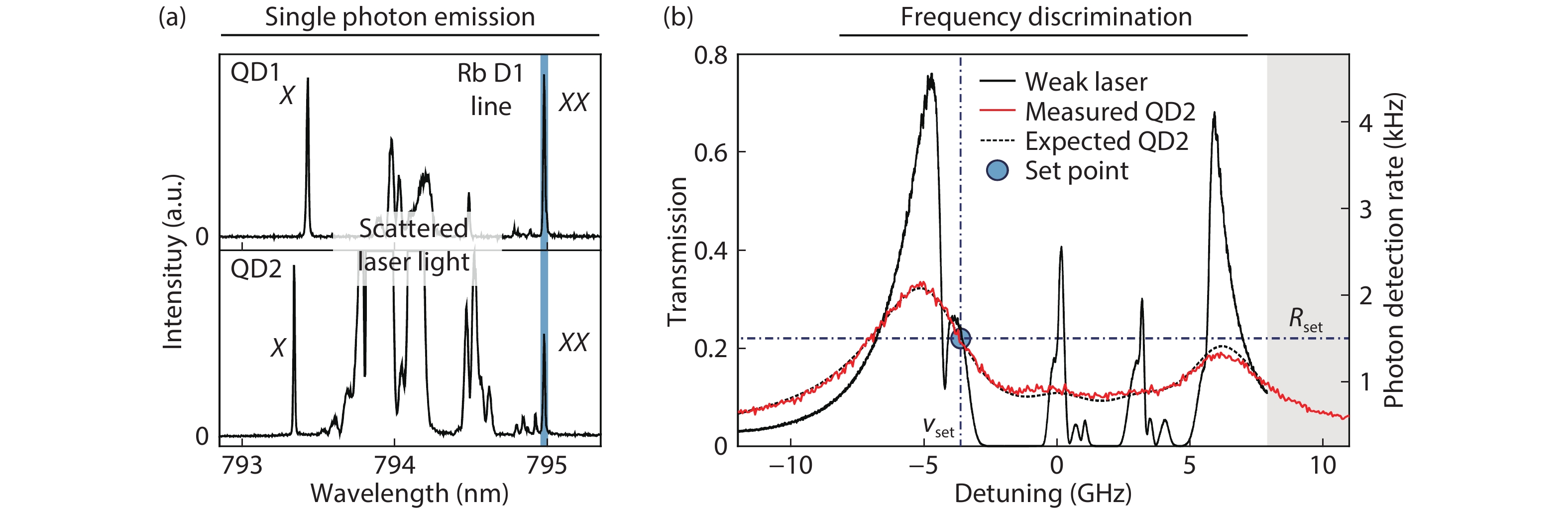
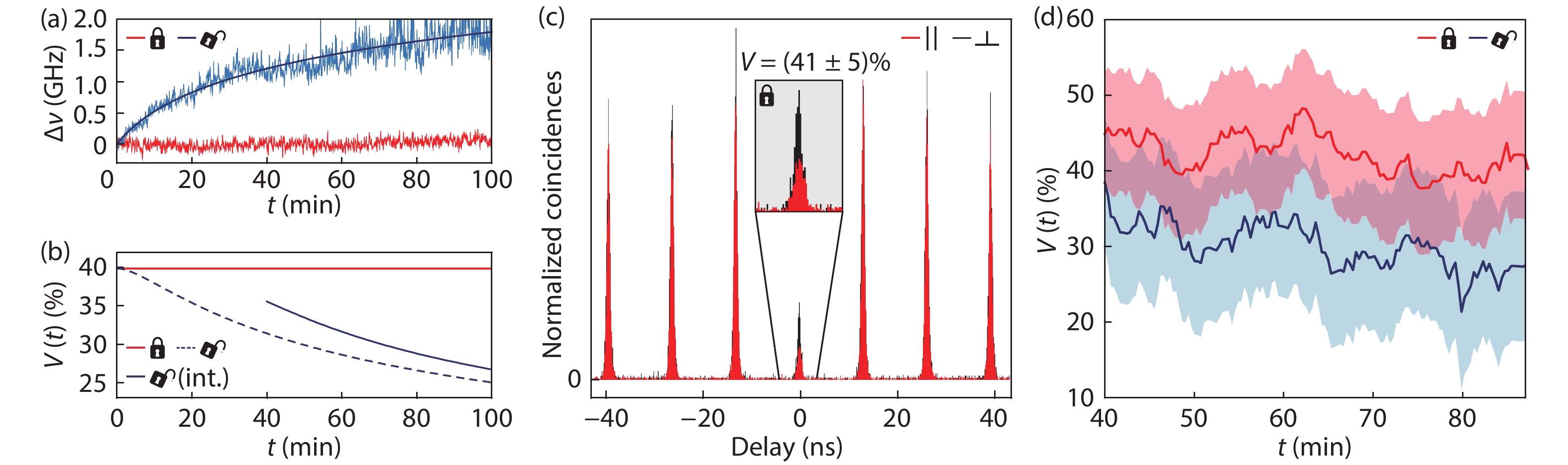
Semiconductor quantum dots are leading candidates for the on-demand generation of single photons and entangled photon pairs. High photon quality and indistinguishability of photons from different sources are critical for quantum information applications. The inability to grow perfectly identical quantum dots with ideal optical properties necessitates the application of post-growth tuning techniques via e.g. temperature, electric, magnetic or strain fields. In this review, we summarize the state-of-the-art and highlight the advantages of strain tunable non-classical photon sources based on epitaxial quantum dots. Using piezoelectric crystals like PMN-PT, the wavelength of single photons and entangled photon pairs emitted by InGaAs/GaAs quantum dots can be tuned reversibly. Combining with quantum light-emitting diodes simultaneously allows for electrical triggering and the tuning of wavelength or exciton fine structure. Emission from light hole exciton can be tuned, and quantum dot containing nanostructure such as nanowires have been piezo-integrated. To ensure the indistinguishability of photons from distant emitters, the wavelength drift caused by piezo creep can be compensated by frequency feedback, which is verified by two-photon interference with photons from two stabilized sources. Therefore, strain tuning proves to be a flexible and reliable tool for the development of scalable quantum dots-based non-classical photon sources.


J. Semicond.
2020, 41(1): 012101 doi: 10.1088/1674-4926/41/1/012101
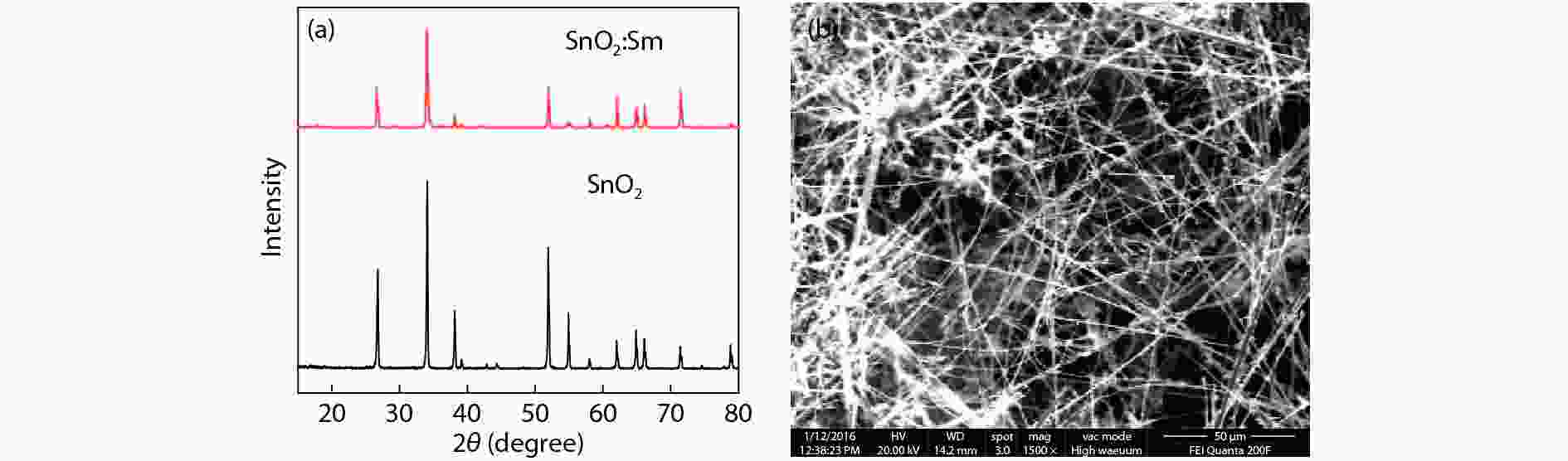
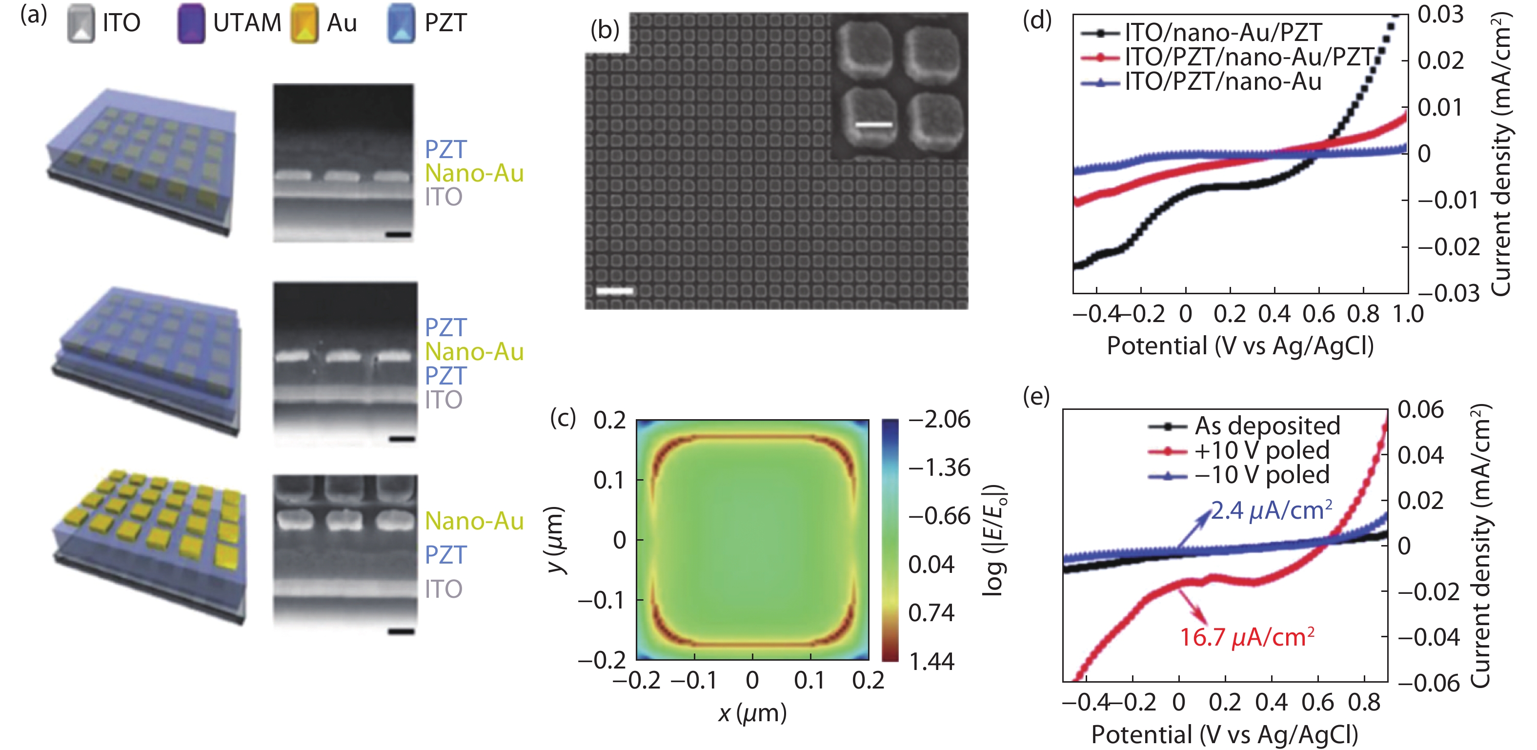
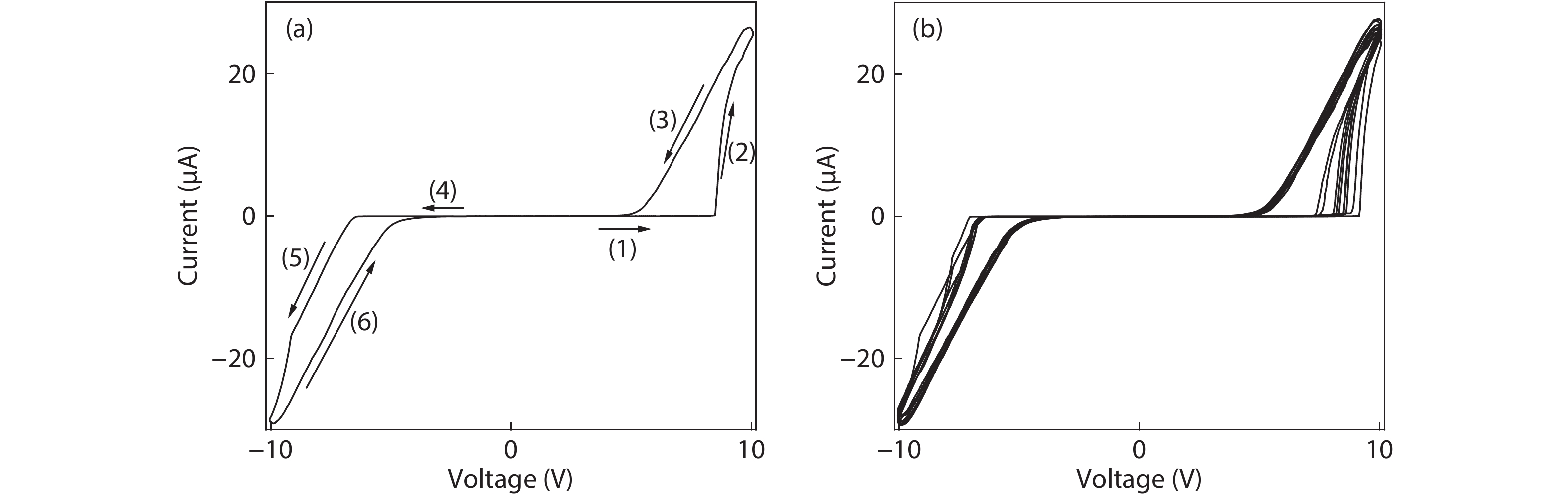
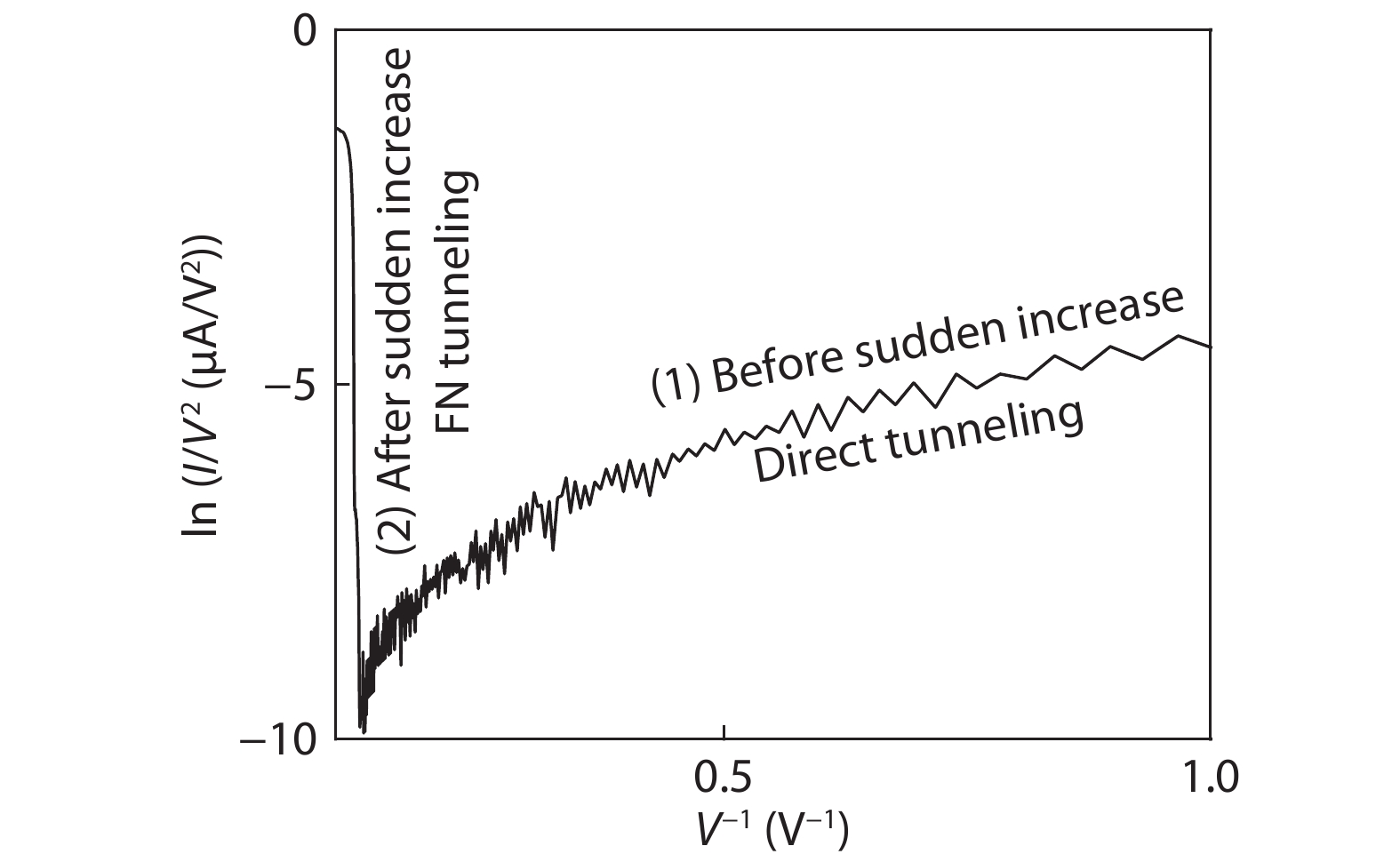
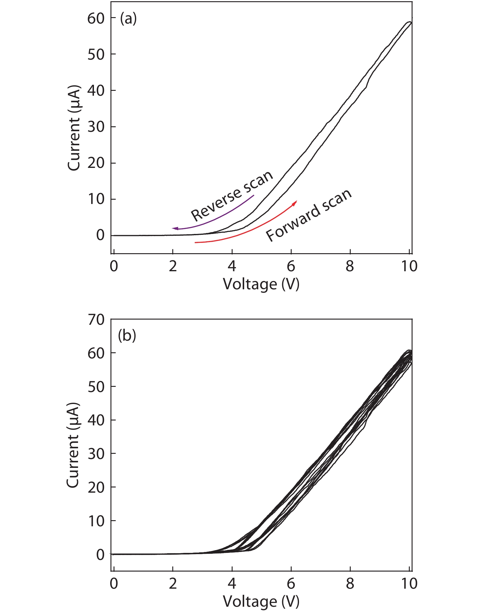
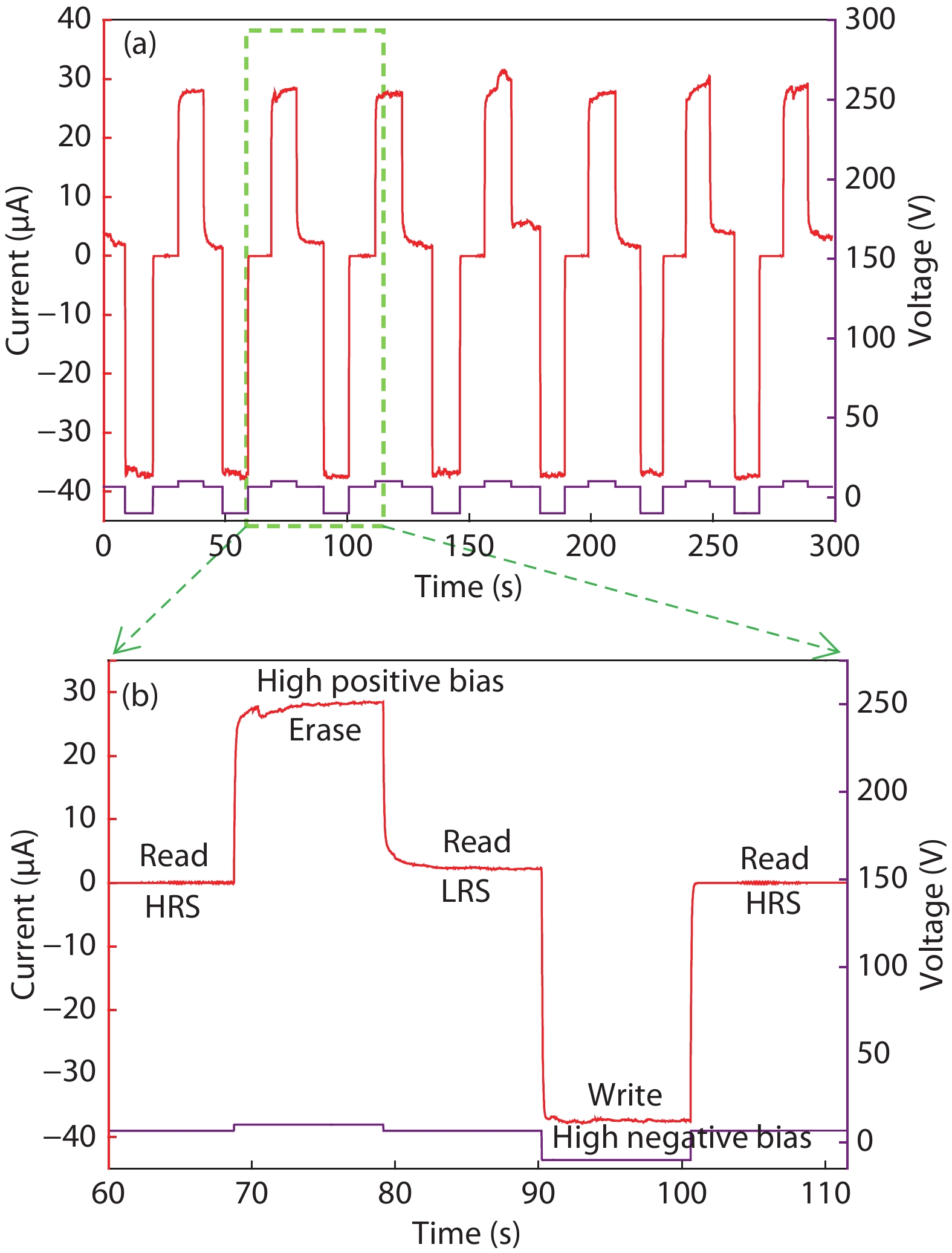
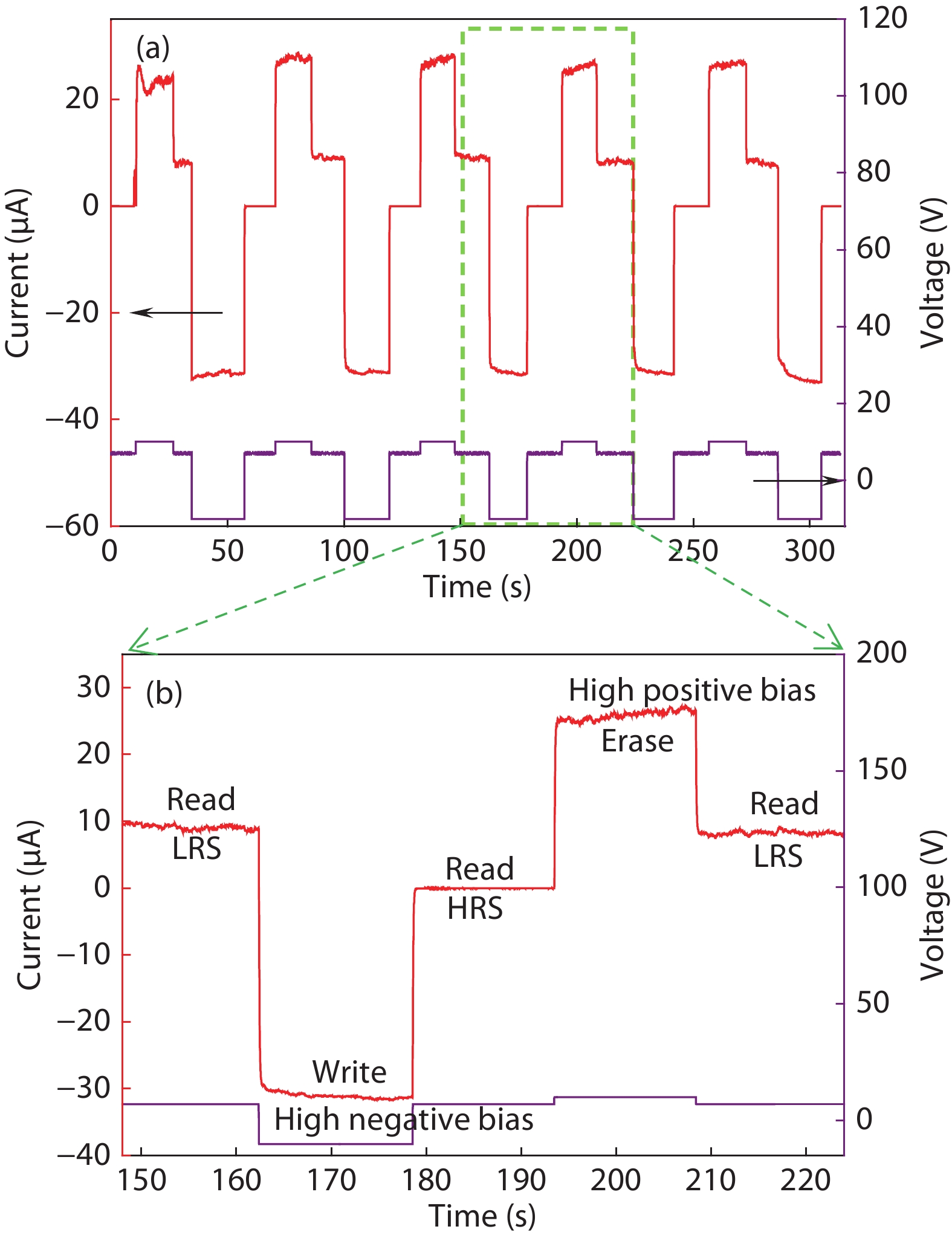
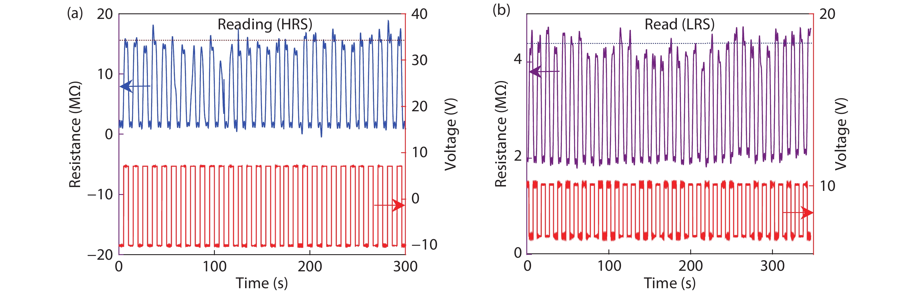
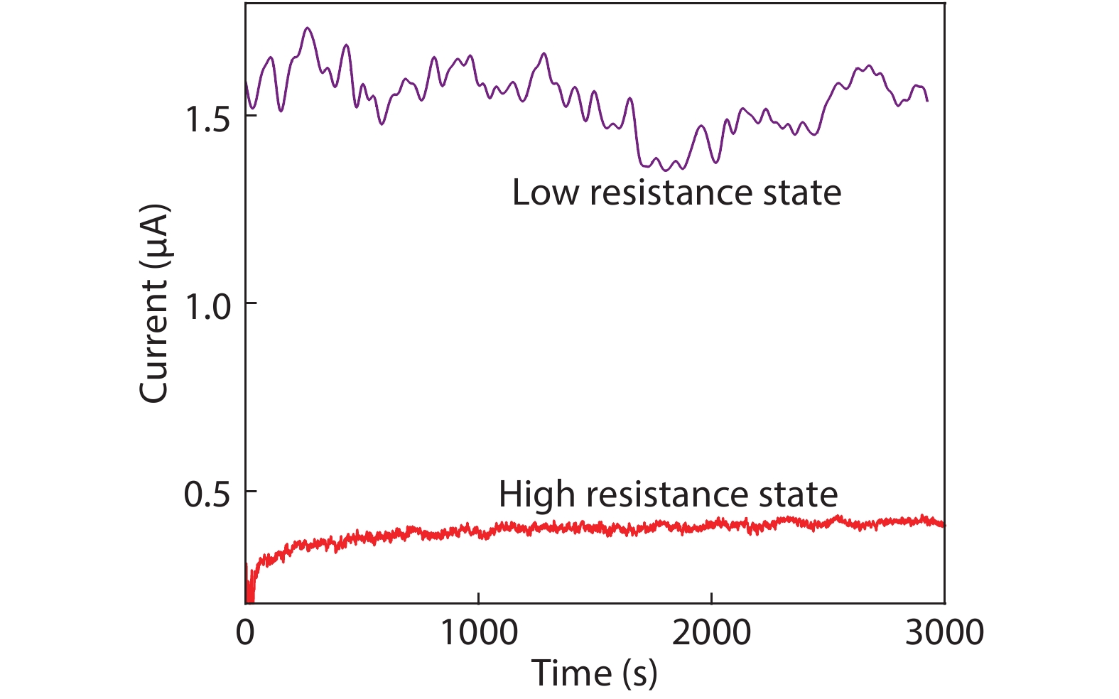
For nanostructure SnO2, it is very difficult for its electric properties to accurately control due to the presence of abundant surface states. The introduction of Sm can improve the traps in surface space charge region of SnO2 nanowires, resulting in a controllable storage charge effect. For the single nanowire-based two-terminal device, two surface state-related back-to-back diodes are formed. At a relatively large voltage, electrons can be injected into the traps in surface space charge region from negative electrode, resulting in a decrease of surface barrier connected with negative electrode, and contrarily electrons can be extracted from the traps in surface space charge region into positive electrode, resulting in an increase of surface barrier connected with positive electrode. The reversible injection and extraction induce a nonvolatile resistive switching memory effect.

J. Semicond.
2020, 41(1): 012301 doi: 10.1088/1674-4926/41/1/012301
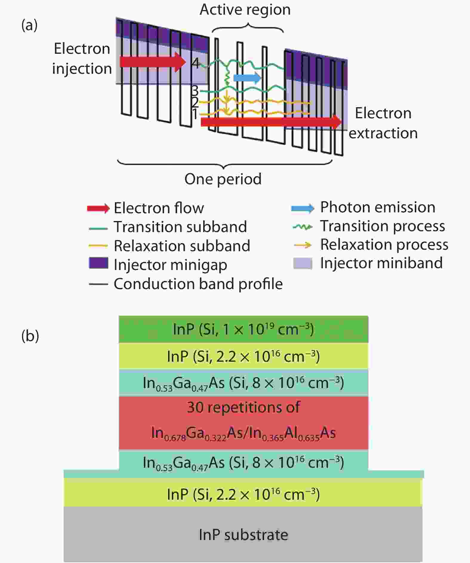
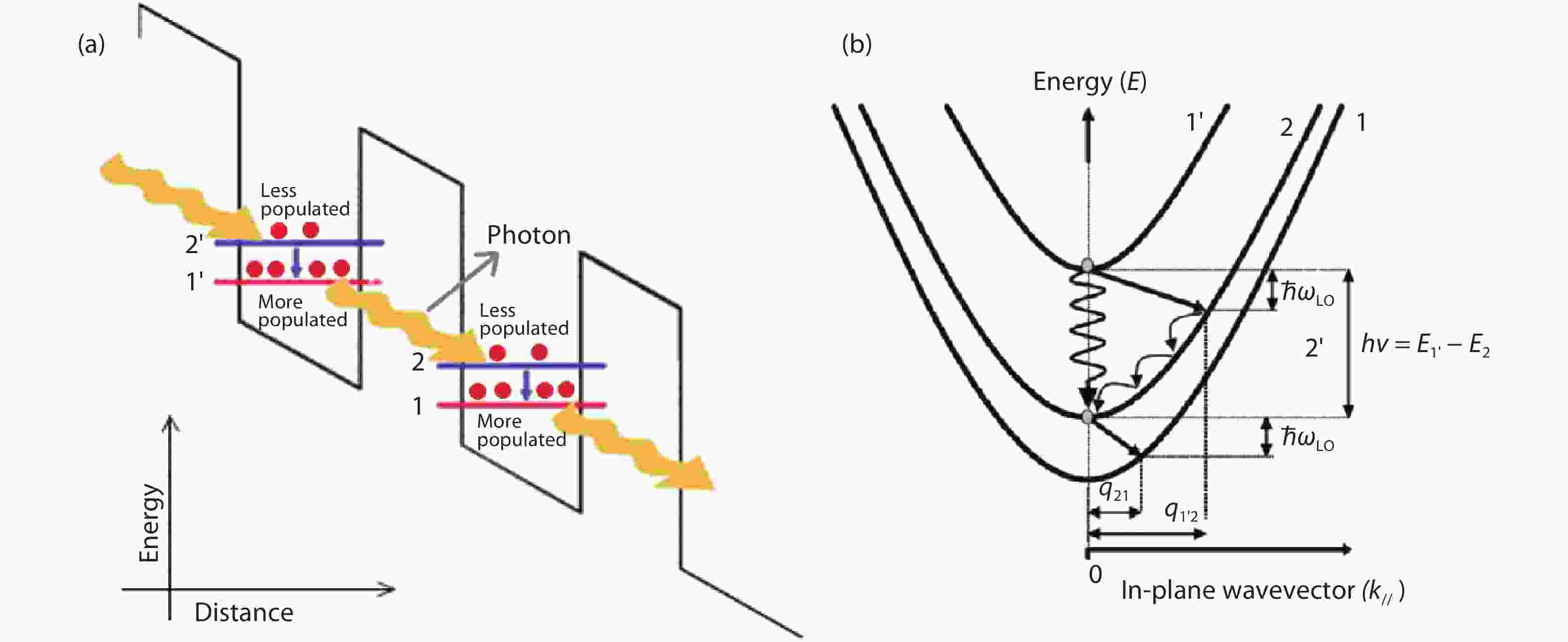
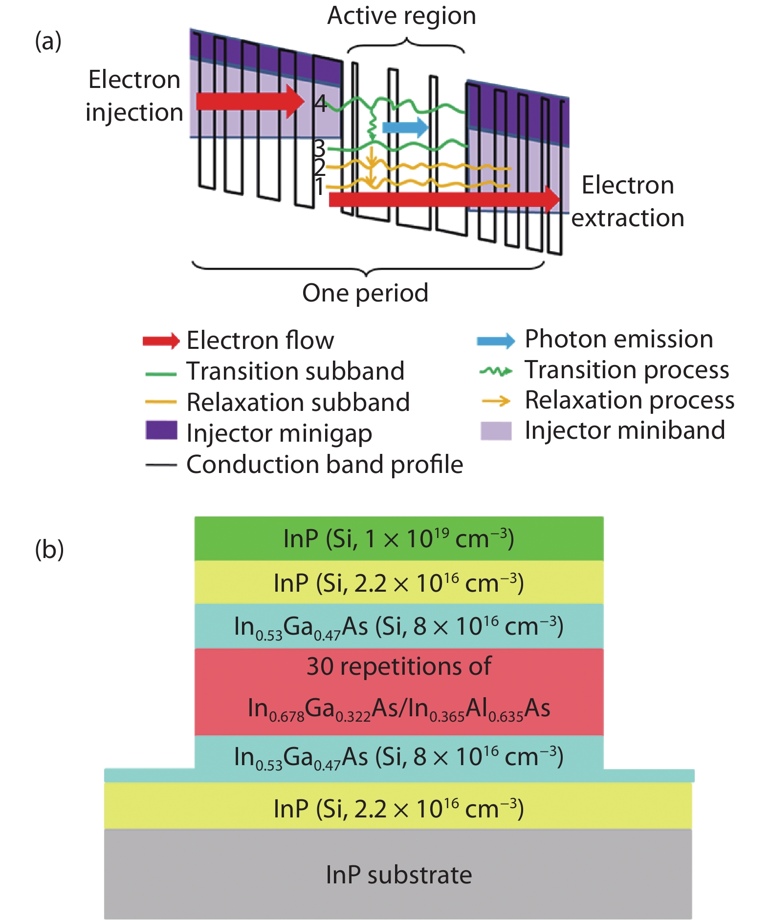
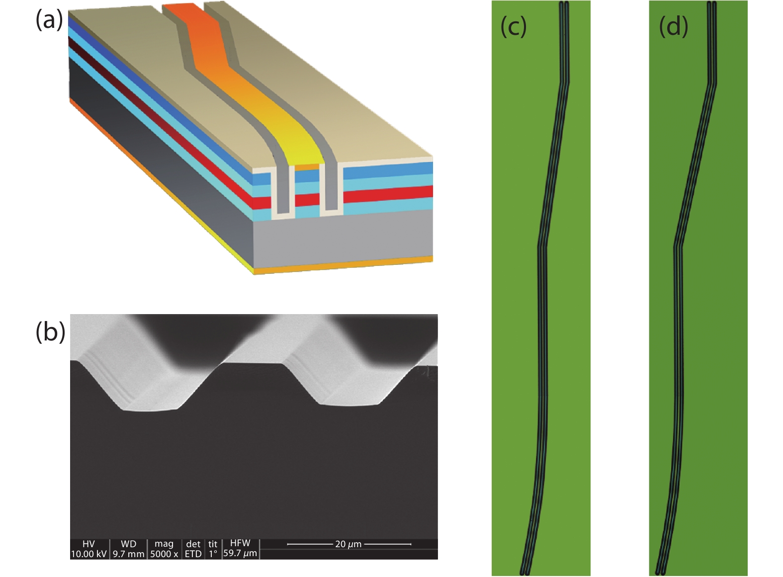
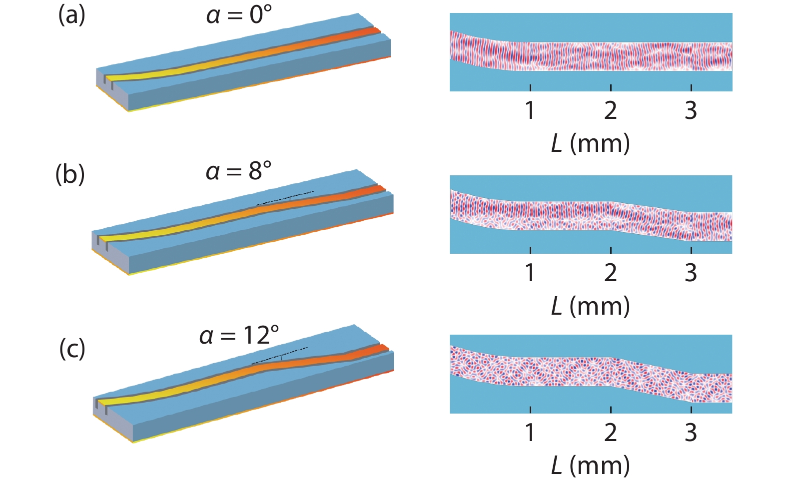
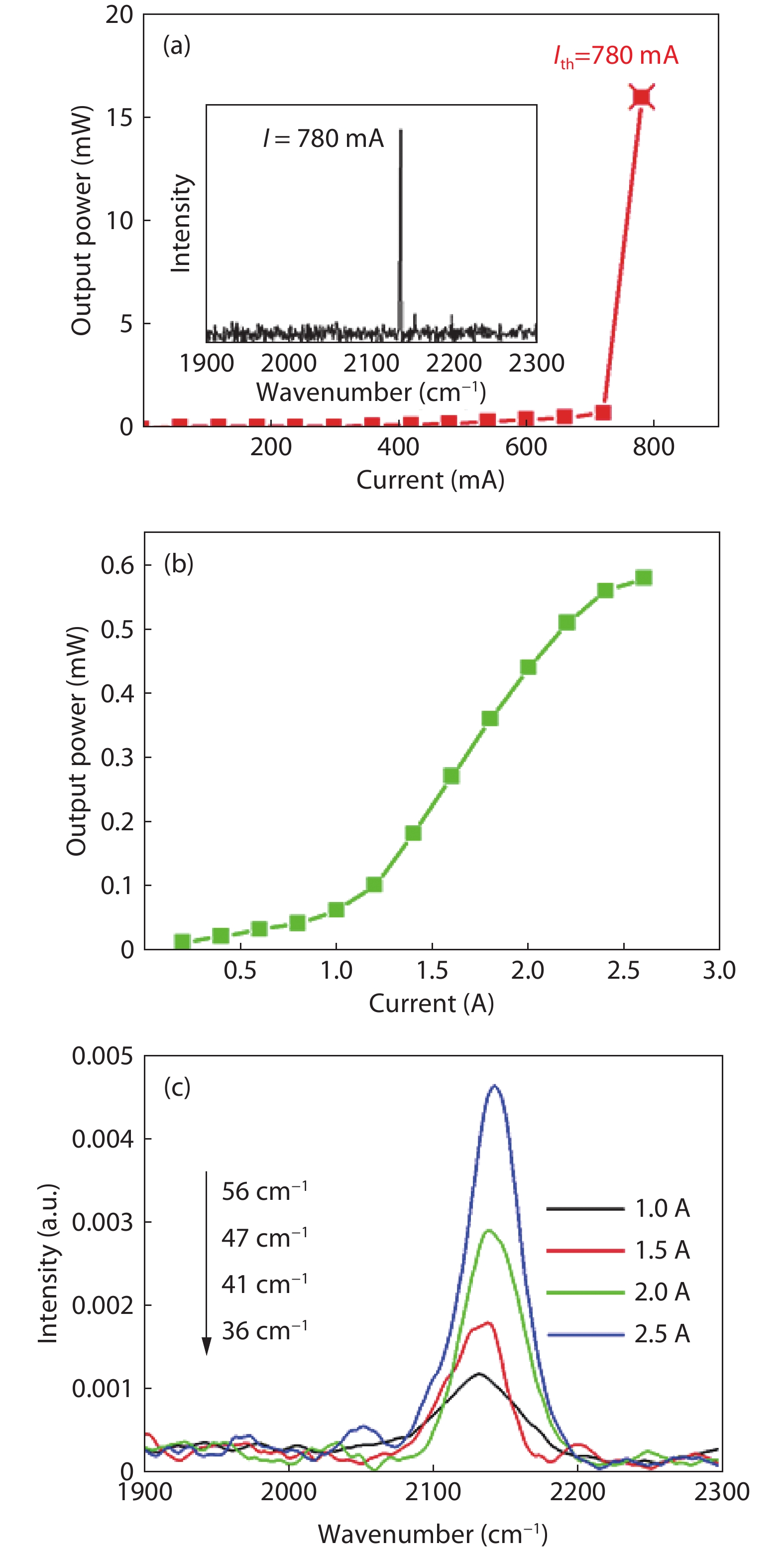
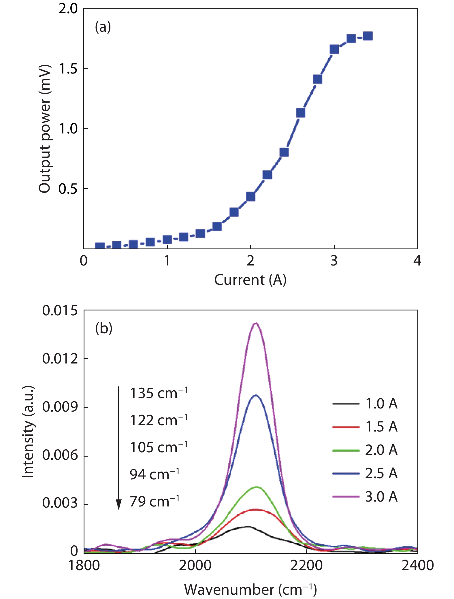
Quantum cascade (QC) superluminescent light emitters (SLEs) have emerged as desirable broadband mid-infrared (MIR) light sources for growing number of applications in areas like medical imaging, gas sensing and national defense. However, it is challenging to obtain a practical high-power device due to the very low efficiency of spontaneous emission in the intersubband transitions in QC structures. Herein a design of ~5 μm SLEs is demonstrated with a two-phonon resonance-based QC active structure coupled with a compact combinatorial waveguide structure which comprises a short straight part adjacent to a tilted stripe and to a J-shaped waveguide. The as-fabricated SLEs achieve a high output power of 1.8 mW, exhibiting the potential to be integrated into array devices without taking up too much chip space. These results may facilitate the realization of SLE arrays to attain larger output power and pave the pathway towards the practical applications of broadband MIR light sources.
J. Semicond.
2020, 41(1): 012302 doi: 10.1088/1674-4926/41/1/012302
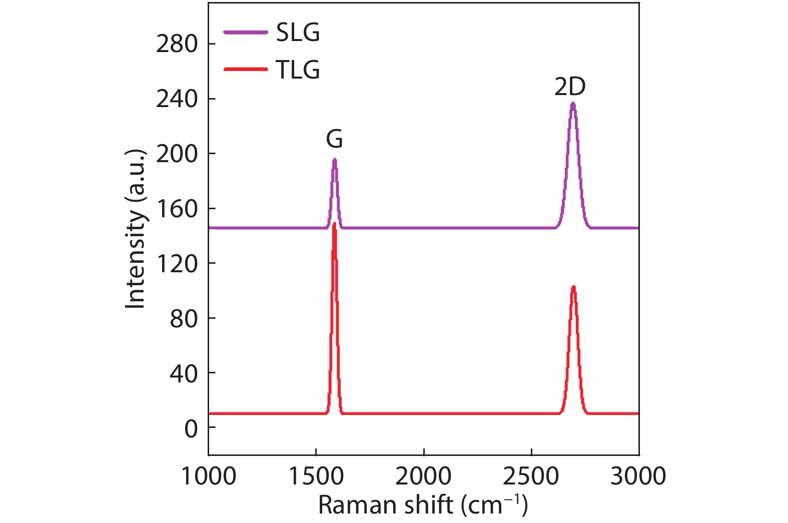
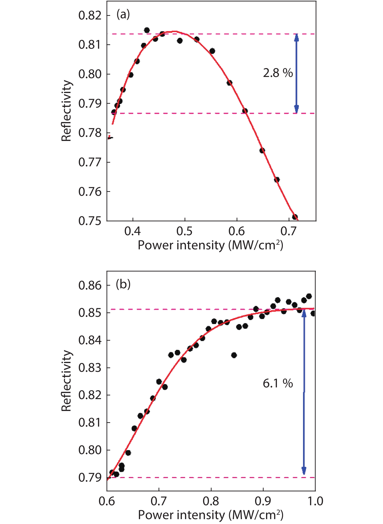
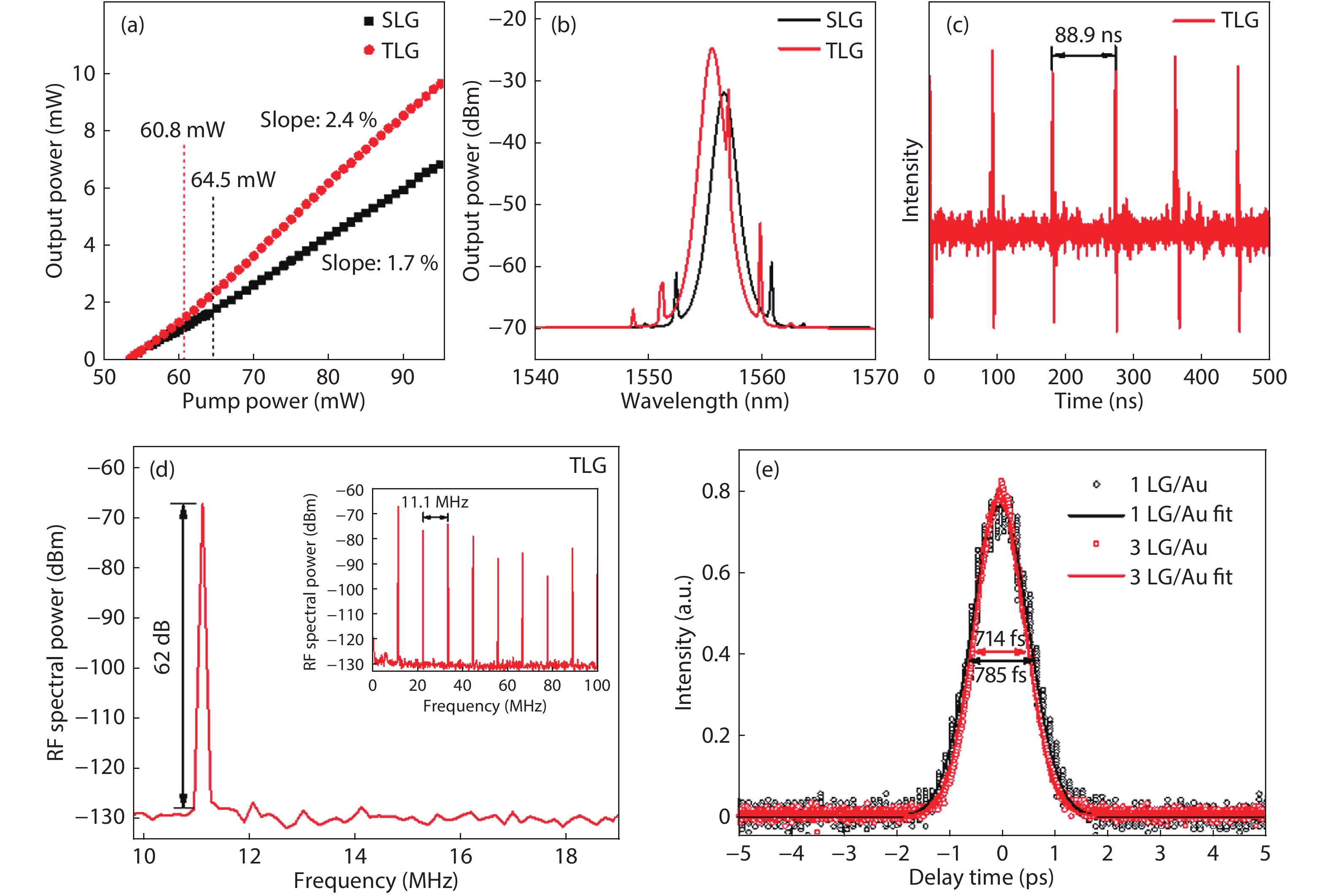
Graphene, as a saturable absorber (SA), has attracted much attention for its application in ultrashort pulse fiber lasers due to its ultrafast interband carrier relaxation and ultra-broadband wavelength operation. Nevertheless, during the stacking process of monolayer graphene layer, the induced nonuniform contact at the interface of graphene layers deteriorate the device performance. Herein, we report the fabrication of graphene saturable absorber mirrors (SAMs) via a one-step transfer process and the realization of the much enlarged modulation depth and the much reduced nonsaturable loss with tri-layer graphene (TLG) than single-layer graphene (SLG) due to the improved uniform contact at the interface. Moreover, the operation of 1550 nm mode-locked Er-doped fiber laser with the TLG SAM exhibits excellent output characteristics of the maximum output power of 9.9 mW, a slope efficiency of 2.4% and a pulse width of 714 fs. Our findings are expected to pave the way toward high-performance ultrashort pulse fiber lasers based on graphene SAs.
J. Semicond.
2020, 41(1): 012701 doi: 10.1088/1674-4926/41/1/012701

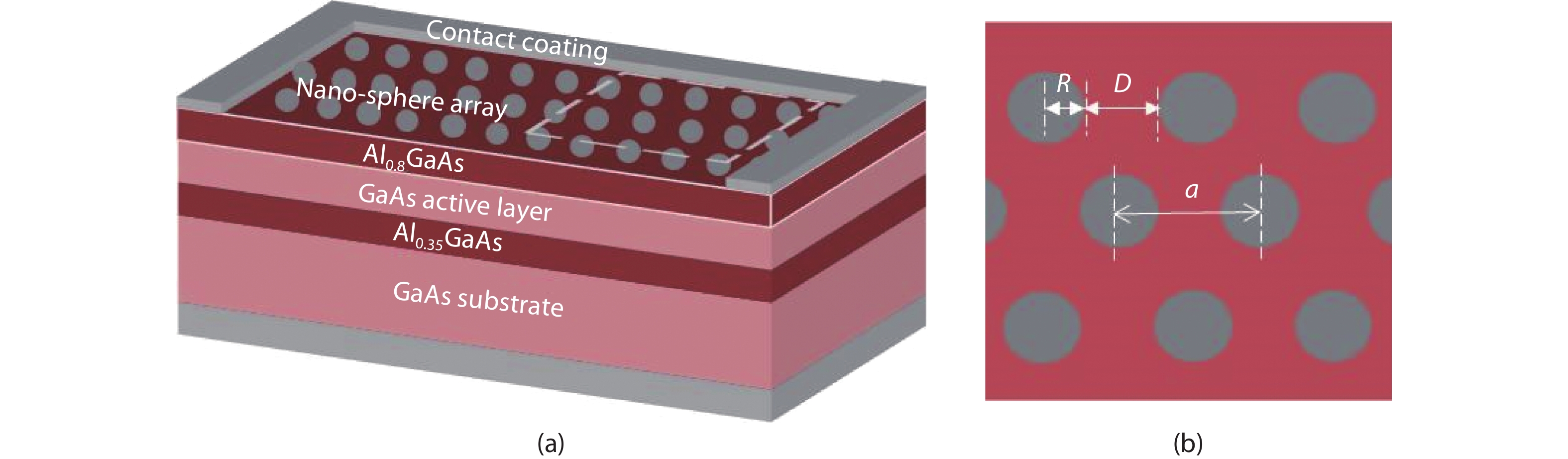
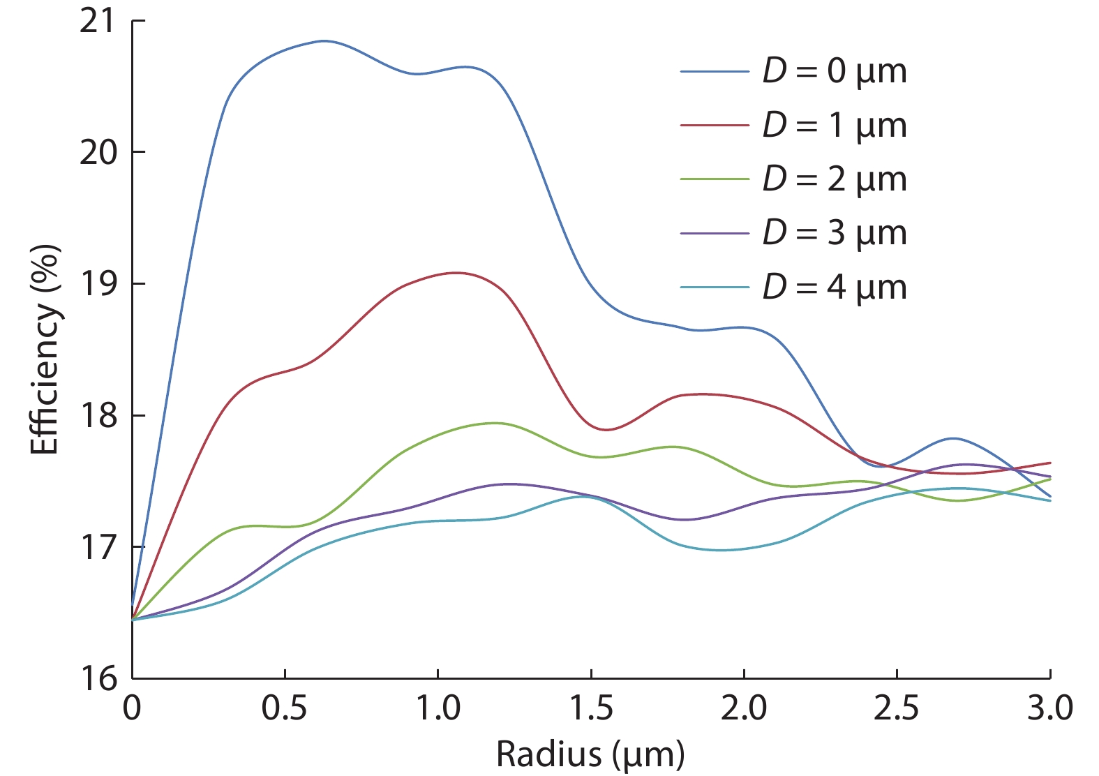
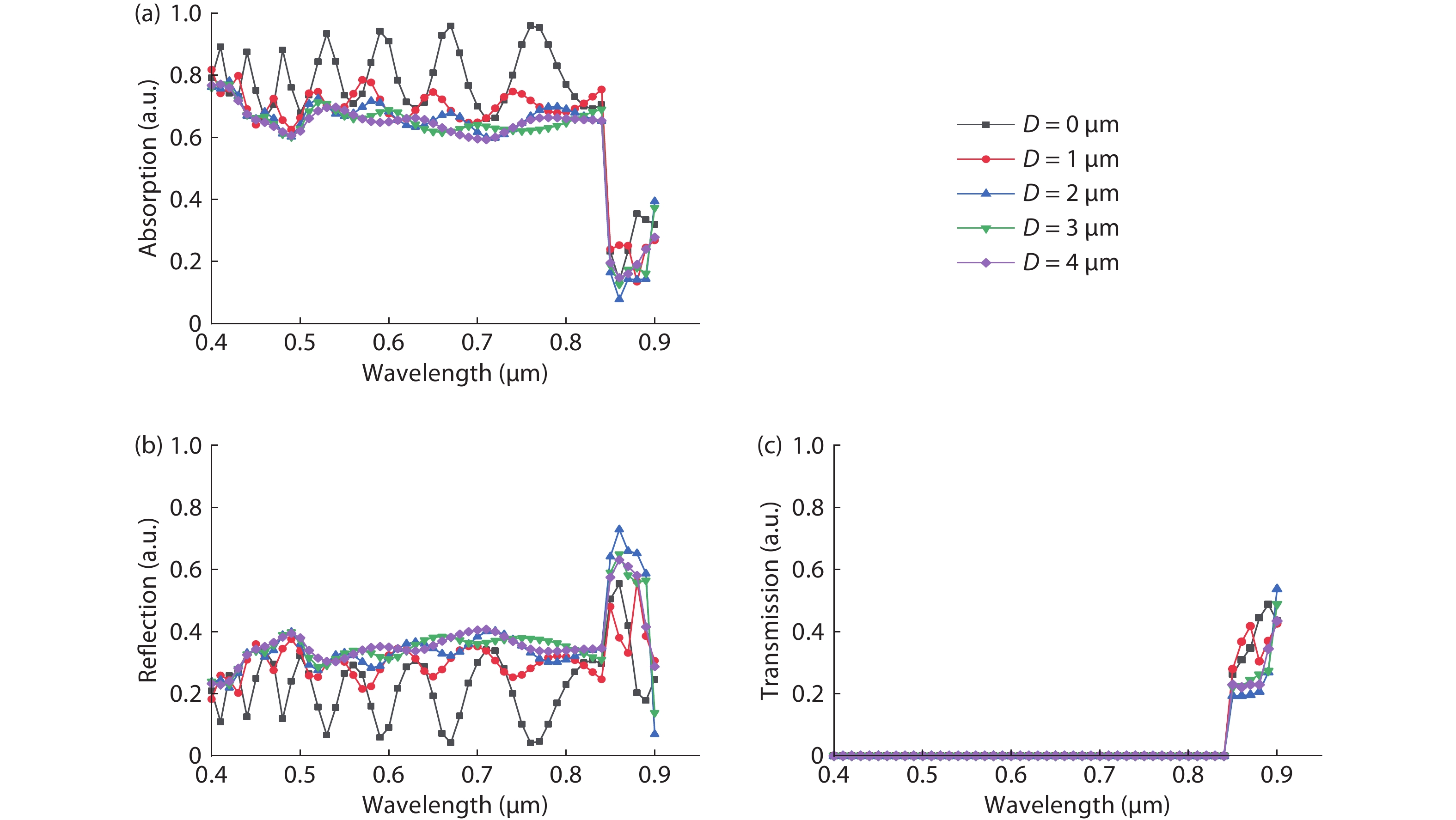
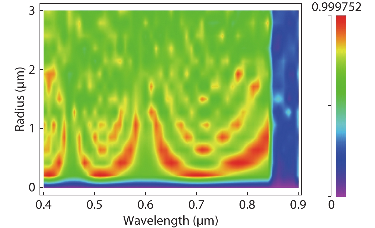
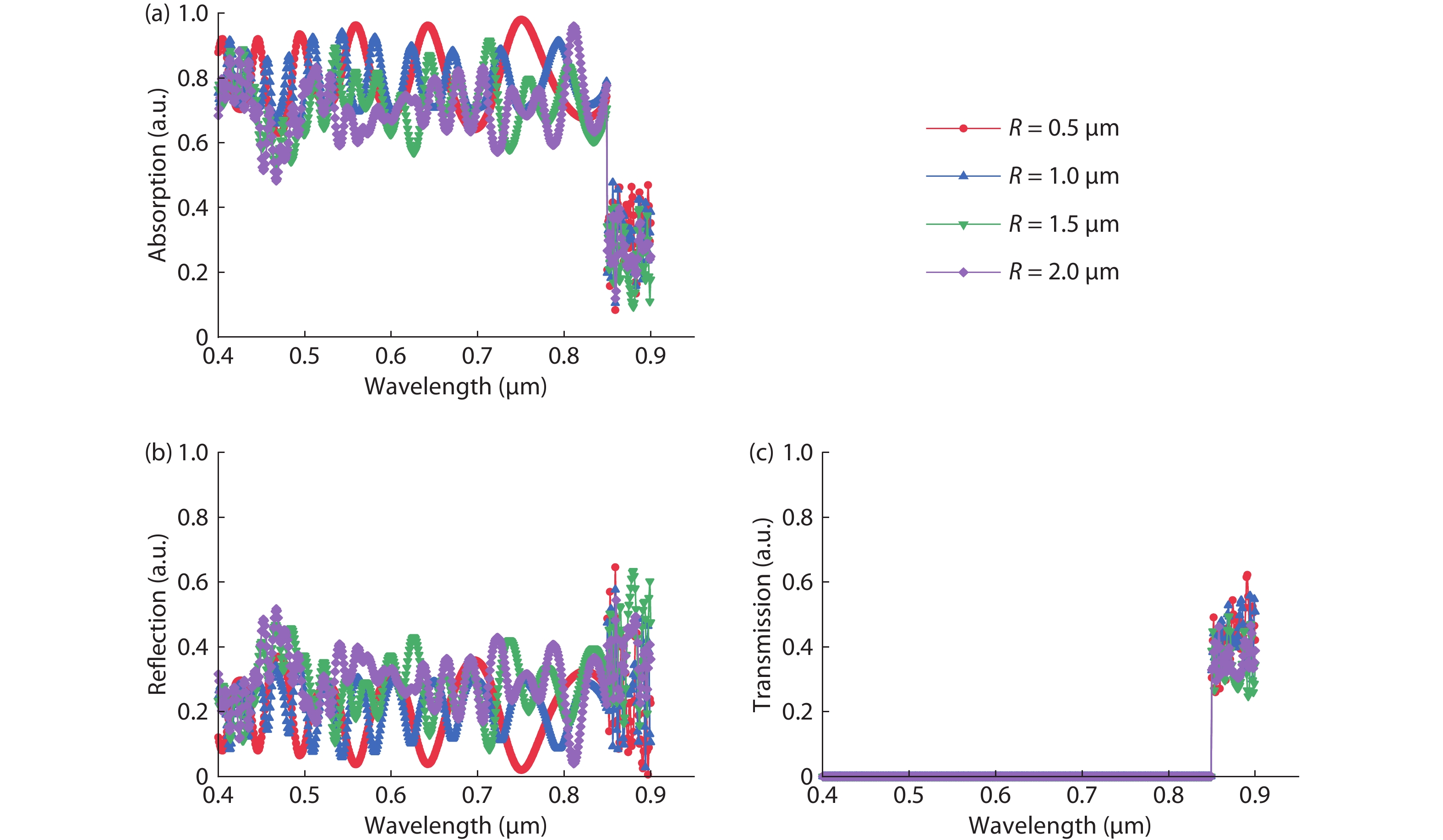
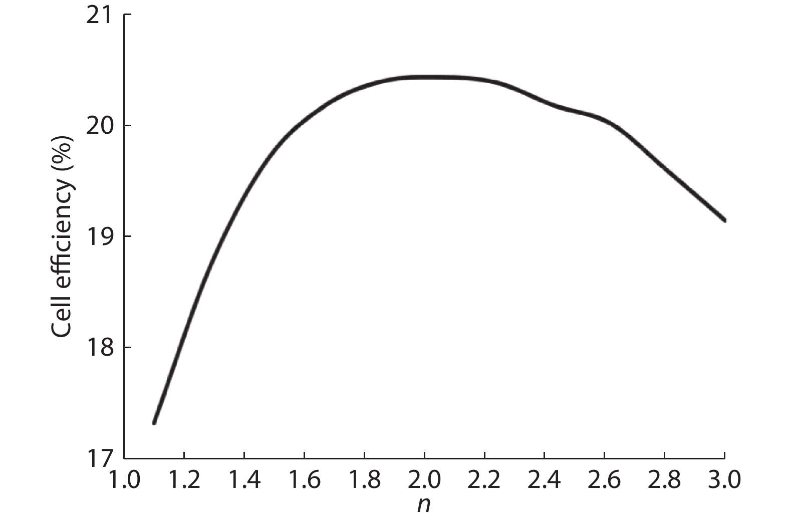
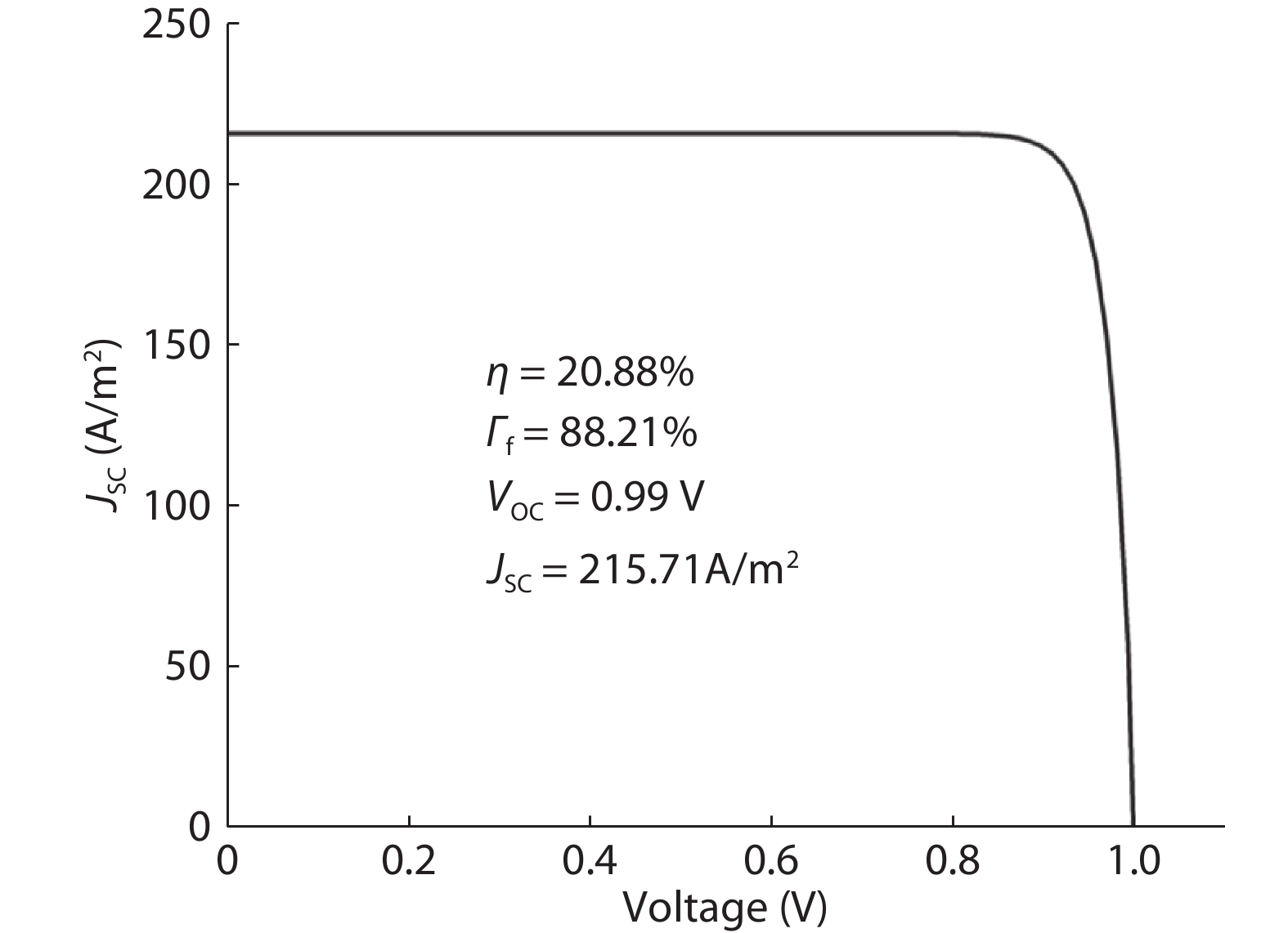
In this paper, we present our efforts on simulating and analyzing the effect of two-dimensional nano-sphere surface array on the characteristic of GaAs solar cells. Based on the scattering and diffraction theory of the photonic crystals, the simulation results show that the distance of adjacent nano-spheres (D) has the pronounced influence on the conversion efficiency and exhibits much poor tolerance, the absolutely conversion efficiency is reduced by exceeding of 2% as the D varies from 0 to 1 μm, in addition, the lower conversion efficiency (< 18%) is exhibited and almost remains unaltered when the D is of > 2 μm. The radius (R) of nano-spheres demonstrates much great tolerance. For D = 0, the solar cells exhibit high conversion efficiency (> 20%) and the efficiency is only varied by less than 1% when R is varied in a very wide region of 0.3–1.2 μm. One can also find out that there is good tolerance for efficiency around the optimal value of refractive index and there is only about 0.2% decrease in final cell efficiency for around ±24% variation in the optimal values, which implys that it does not demand high precision processing equipment and the whole nano-sphere array could be fully complemented using self-assembled chemical methods.