Towards a sustainable healthcare system, the clinical-grade diagnostic platform should be decentralized into low-cost consumer-grade handheld devices, for broadly and early disease screening and diagnosis. The joint advancement of CMOS biosensors and signal-processing capability has recently transformed bulky laboratory instruments into handheld devices, leading to cost, size and weight reduction by orders of magnitude. This article gives a glimpse of the lab-on-CMOS in-vitro diagnostic (IVD) tools for point-of-care applications.
Issue Browser
Volume 41, Issue 11,
Nov 2020
J. Semicond.
2020, 41(11): 111401 doi: 10.1088/1674-4926/41/11/111401

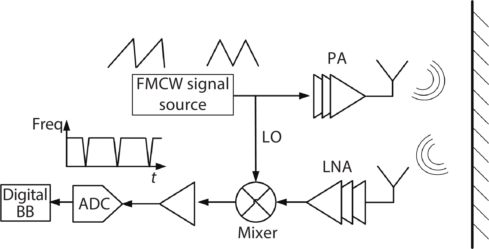
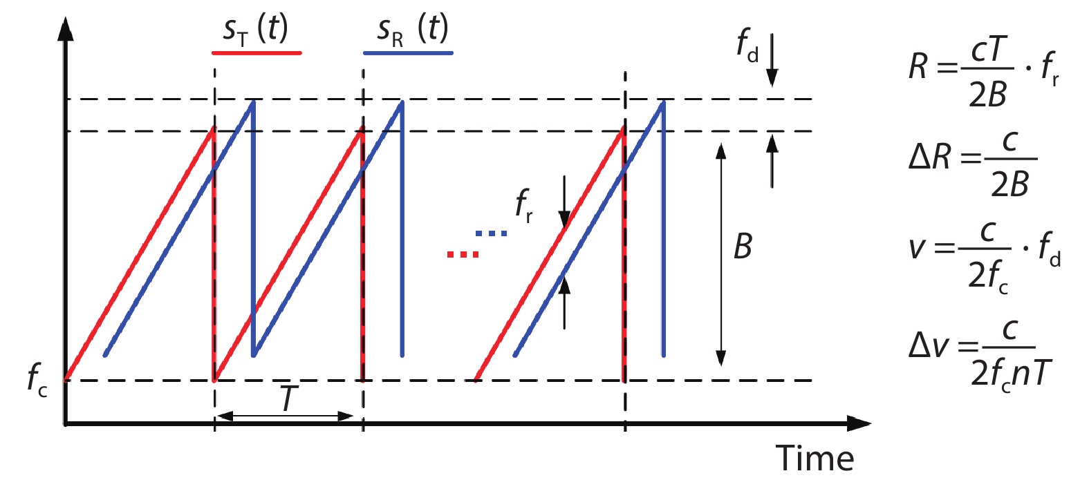
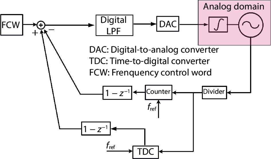
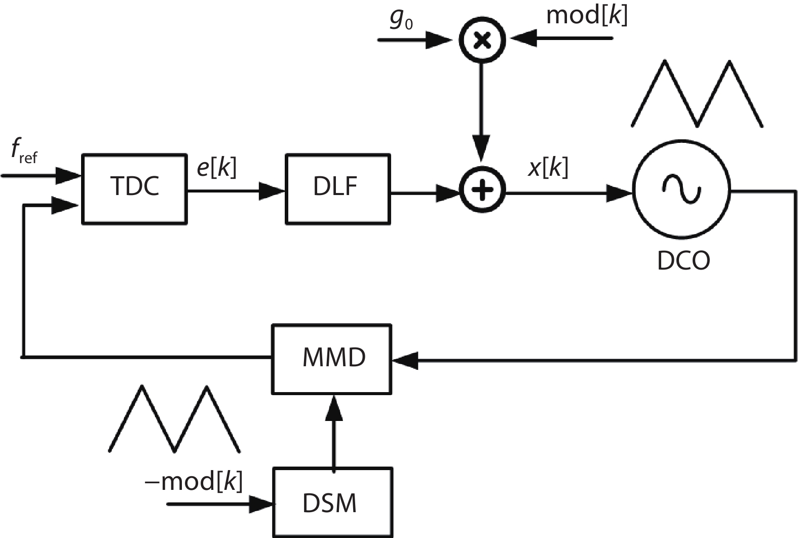
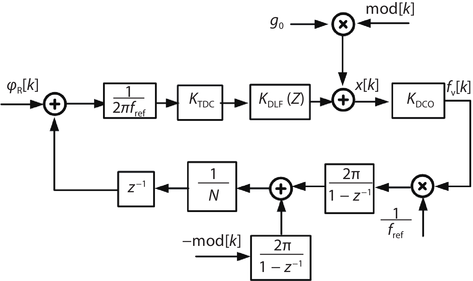
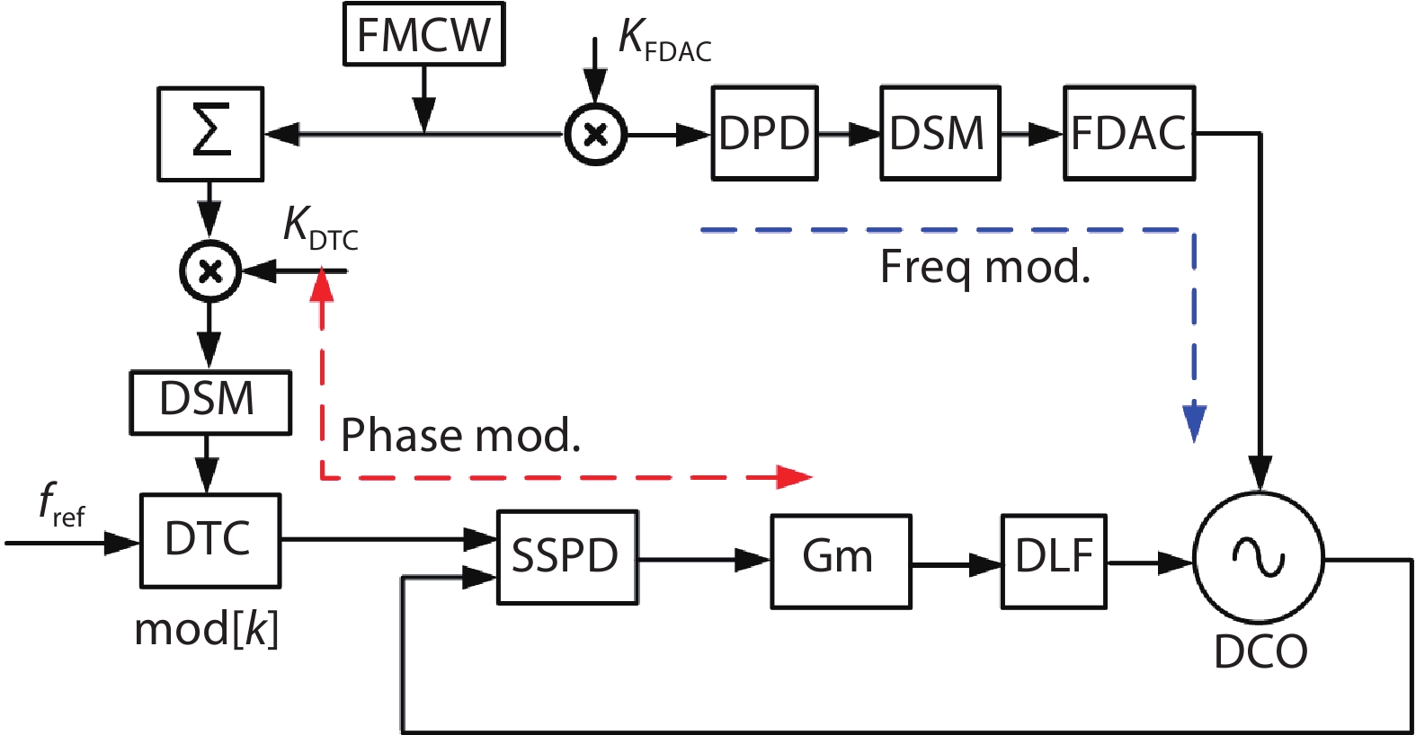
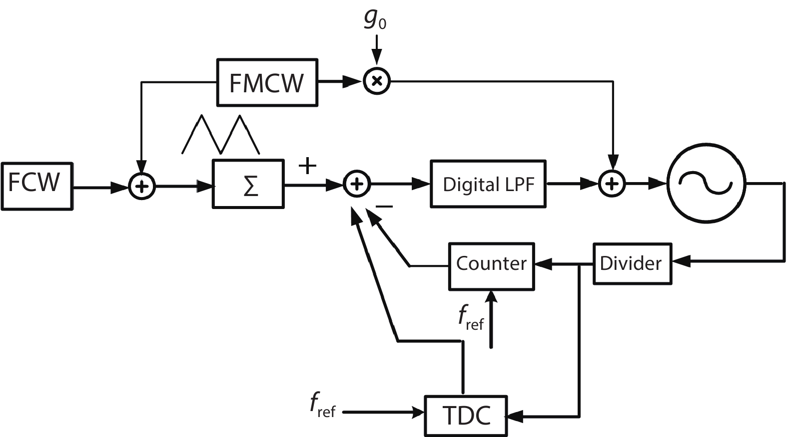
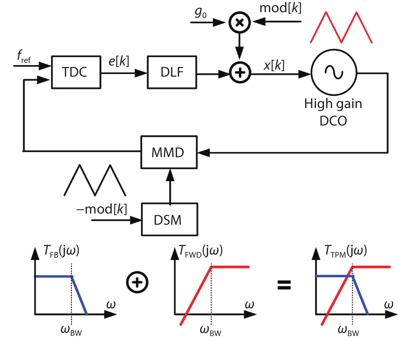
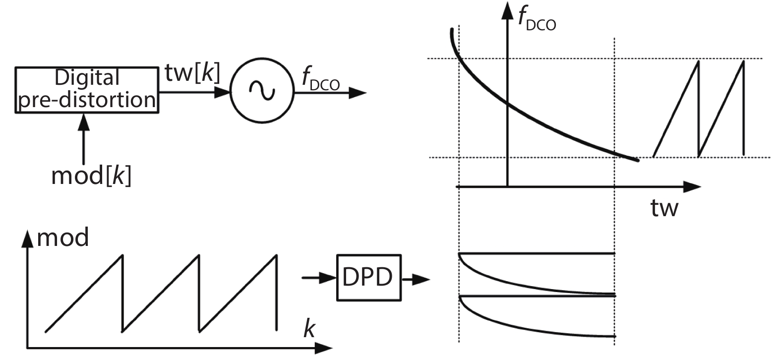
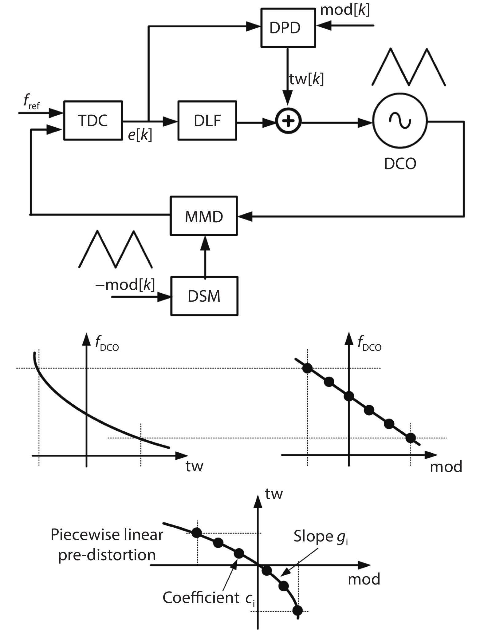
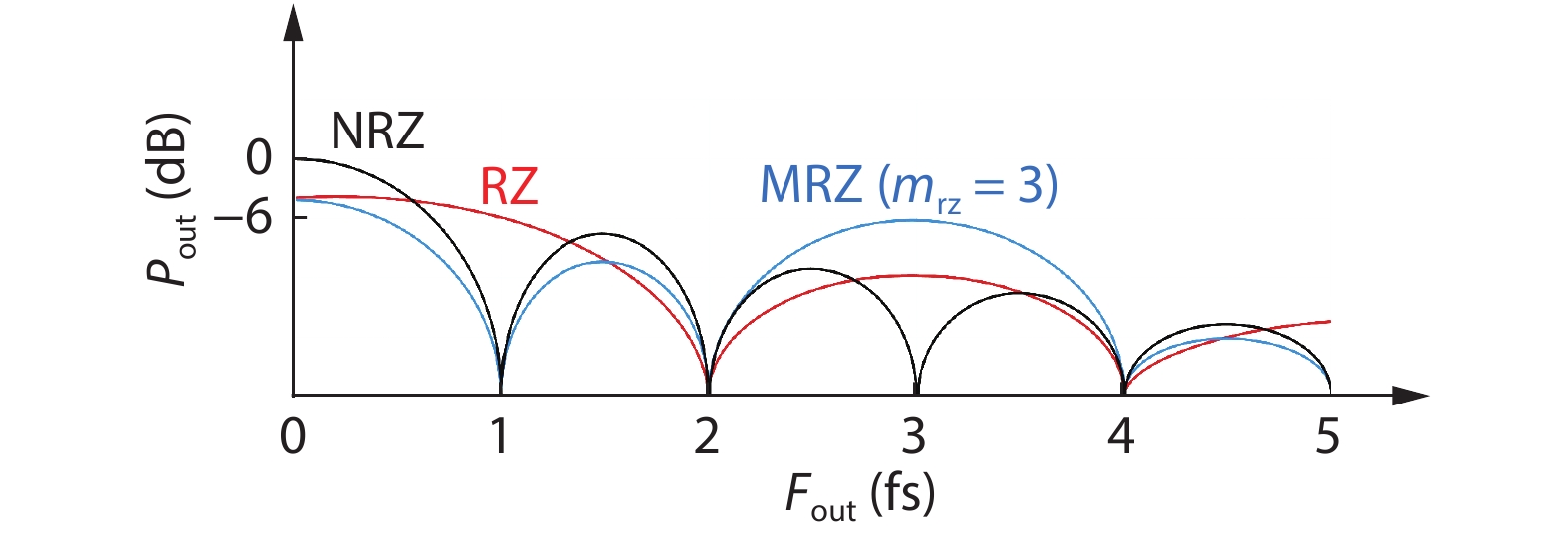
FMCW radars with high resolution necessities the generation of highly linear, low phase noise, and low spur chirp signals with large bandwidth and a short modulation period. This paper reviews recent research progress on silicon-based FMCW signal generators, identifies advances in architecture, fundamental design, performance analysis, and applications of the FMCW synthesizer.


J. Semicond.
2020, 41(11): 111402 doi: 10.1088/1674-4926/41/11/111402
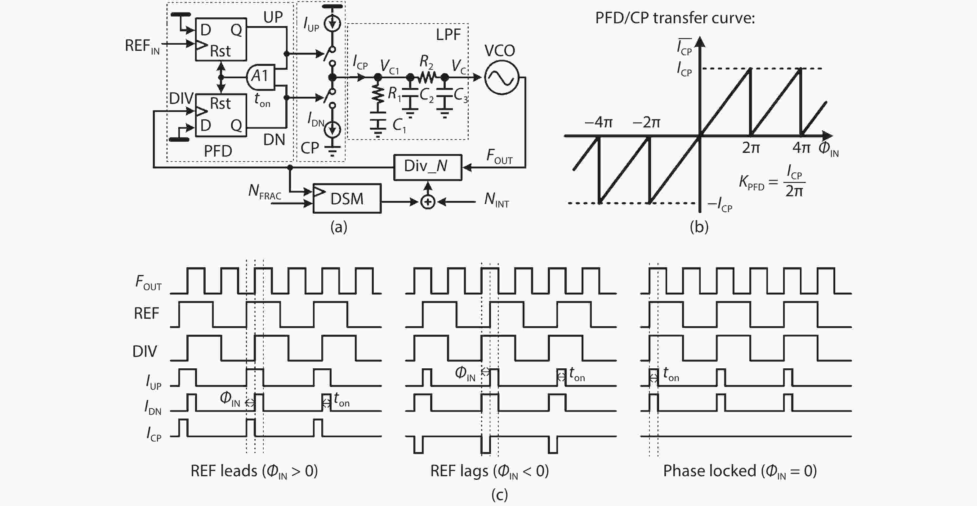
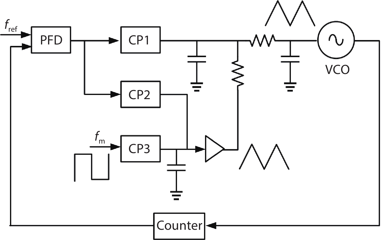
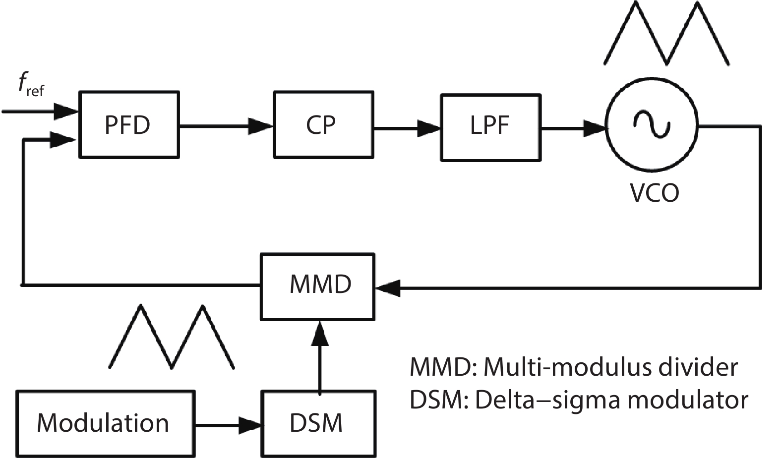
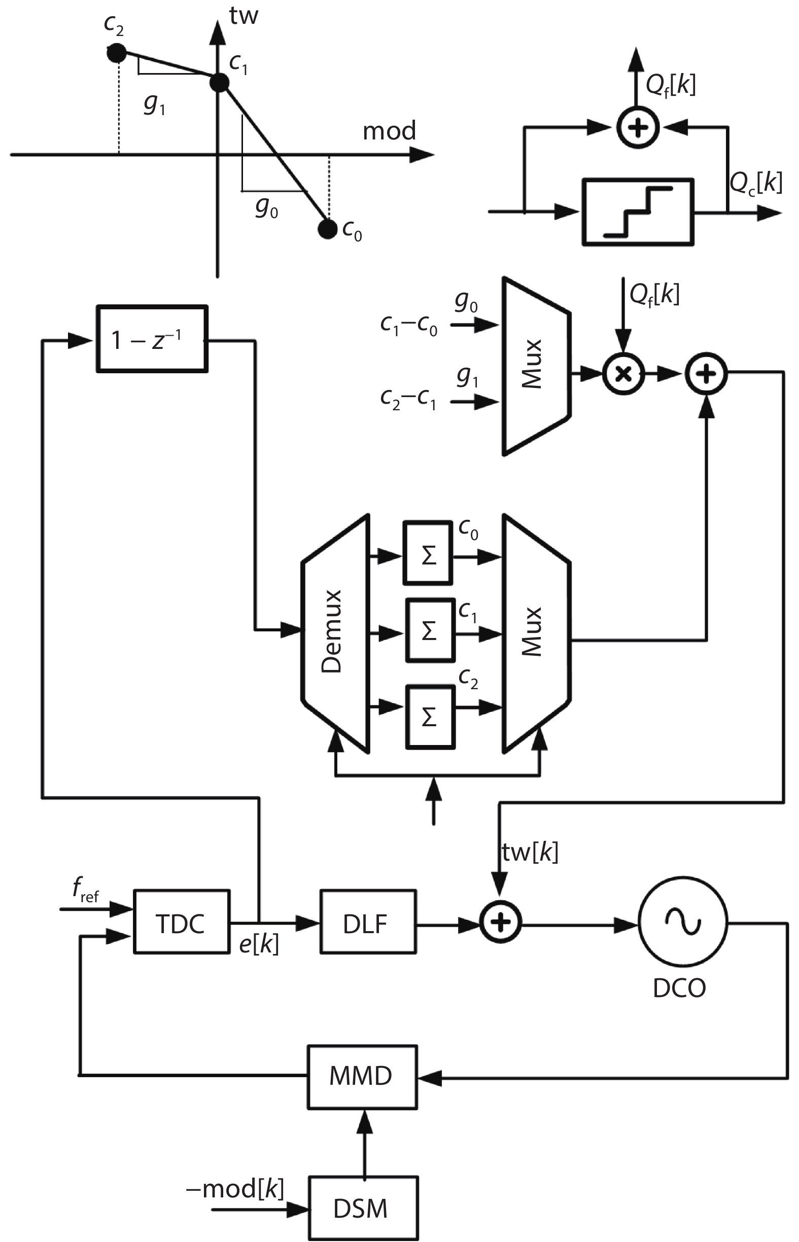
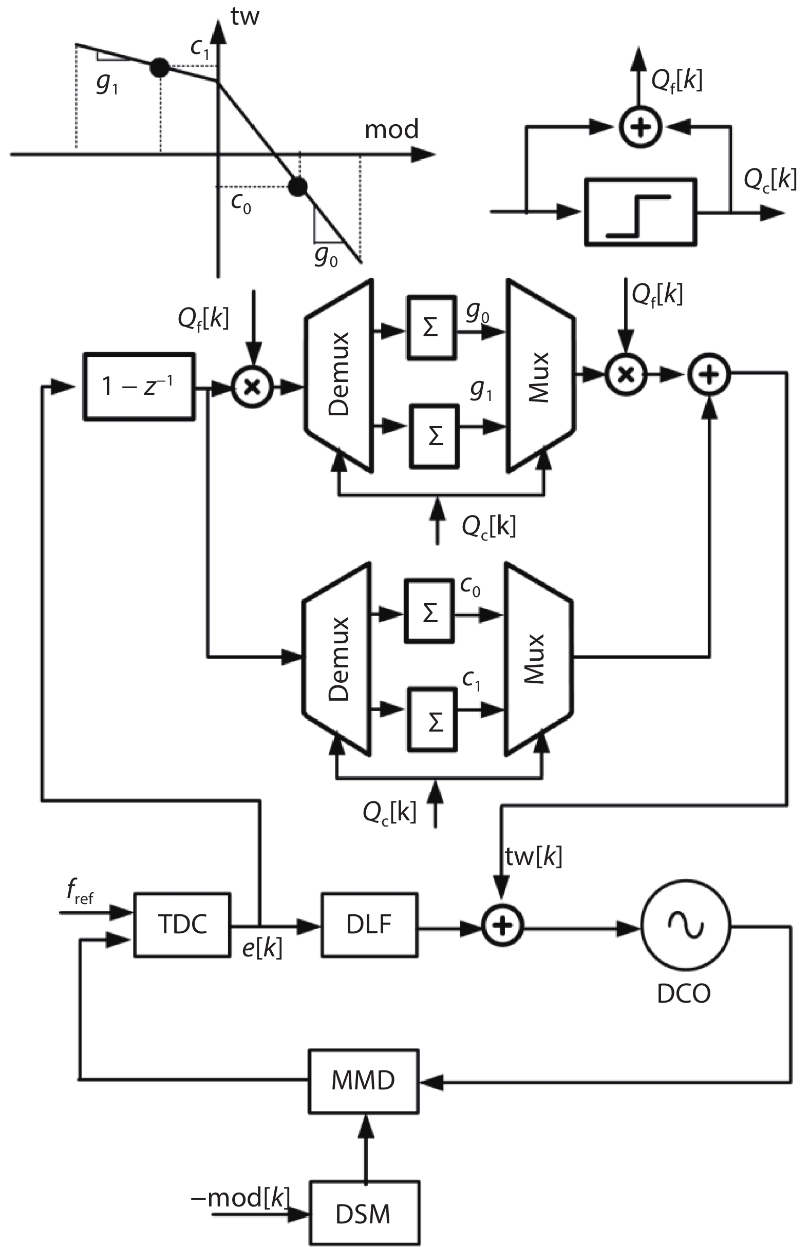
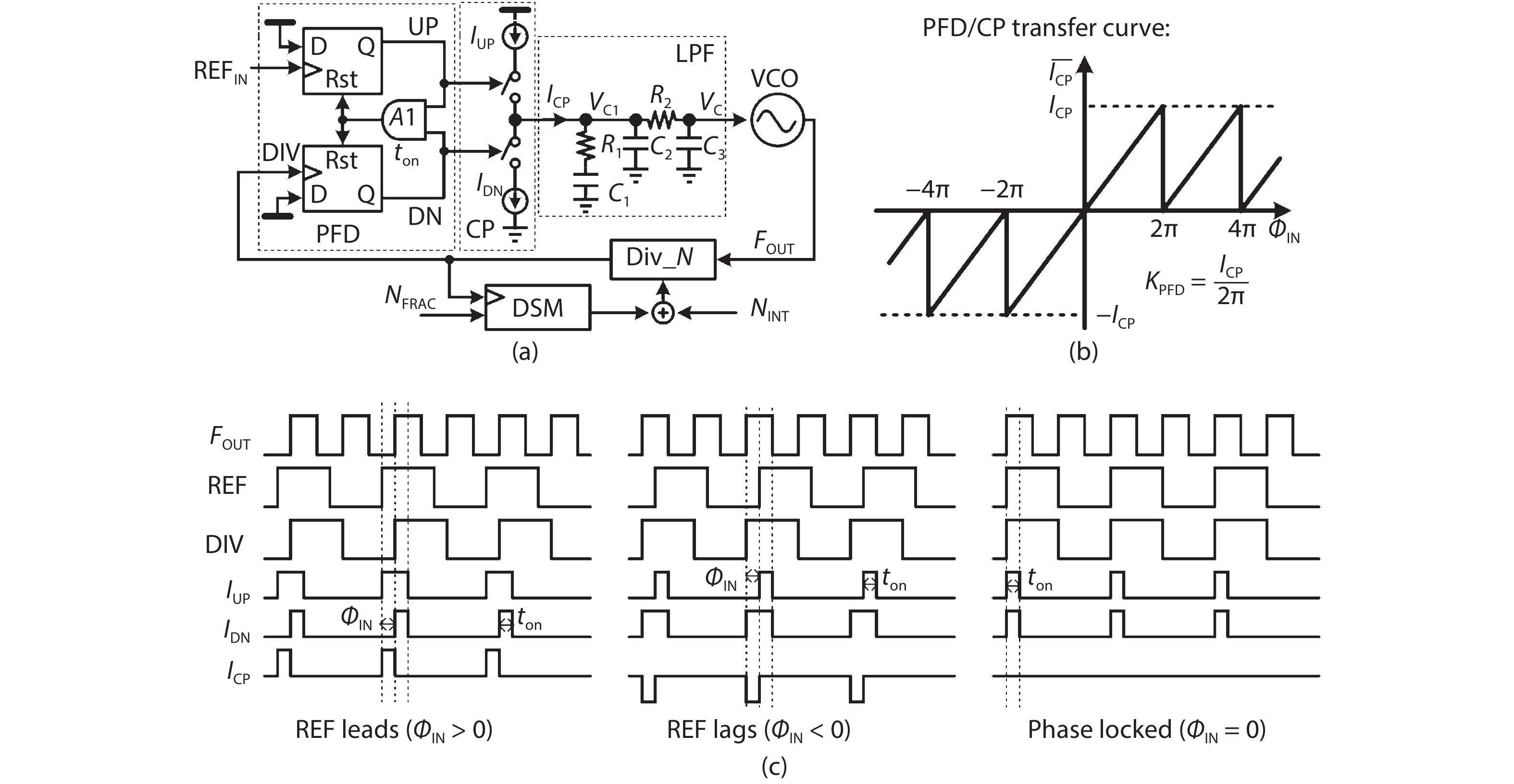
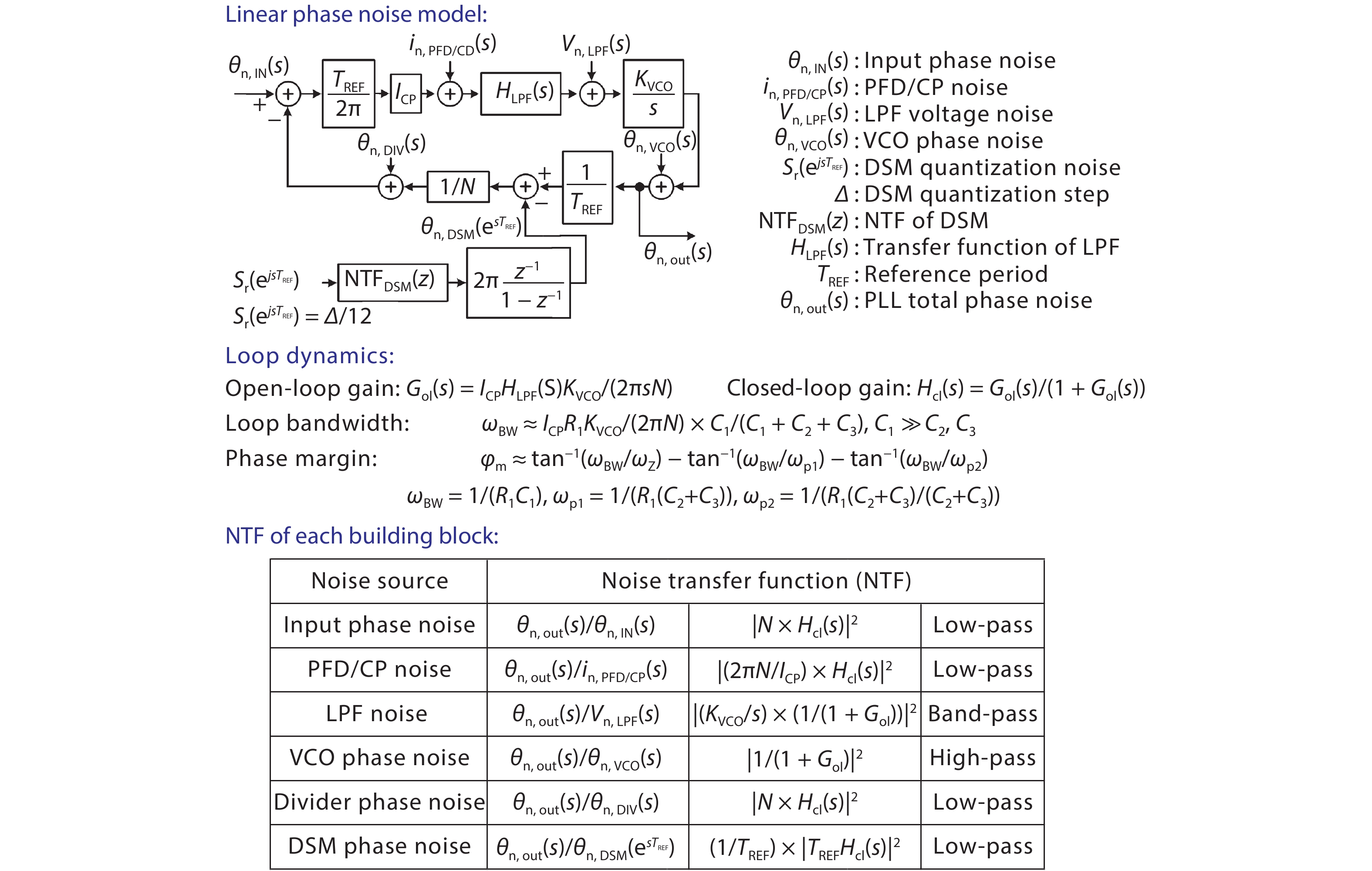
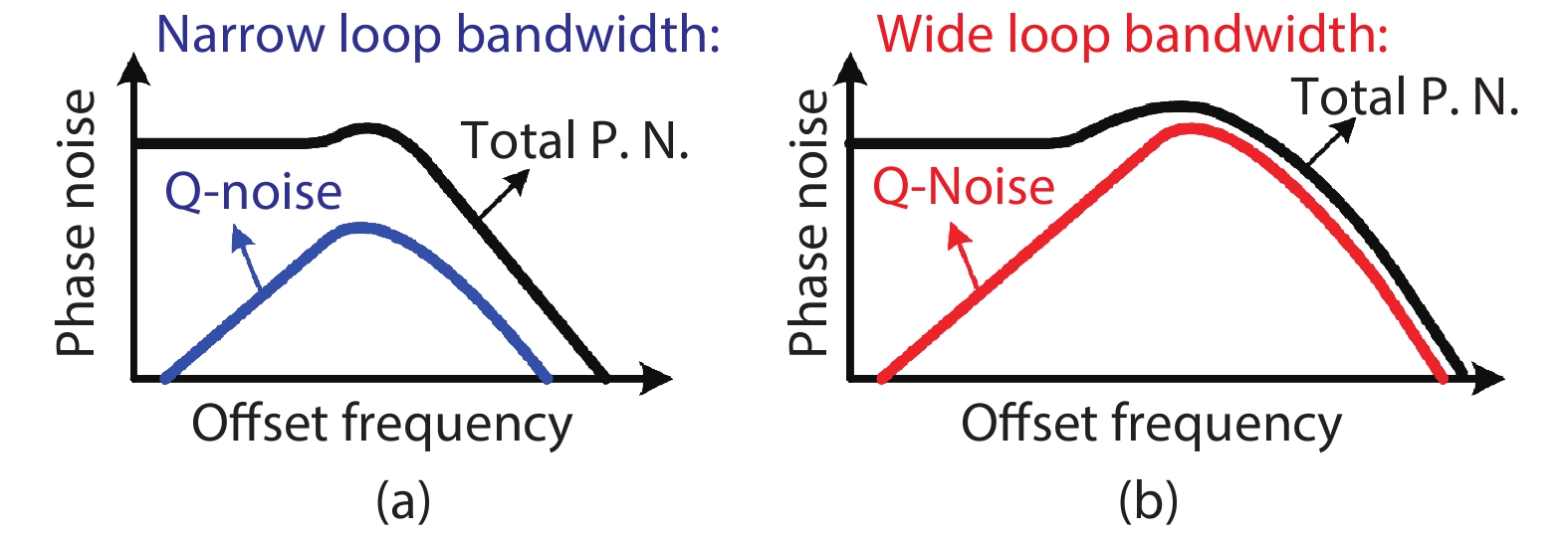
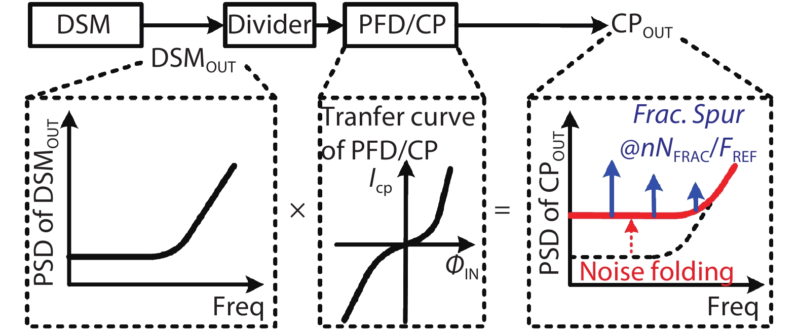
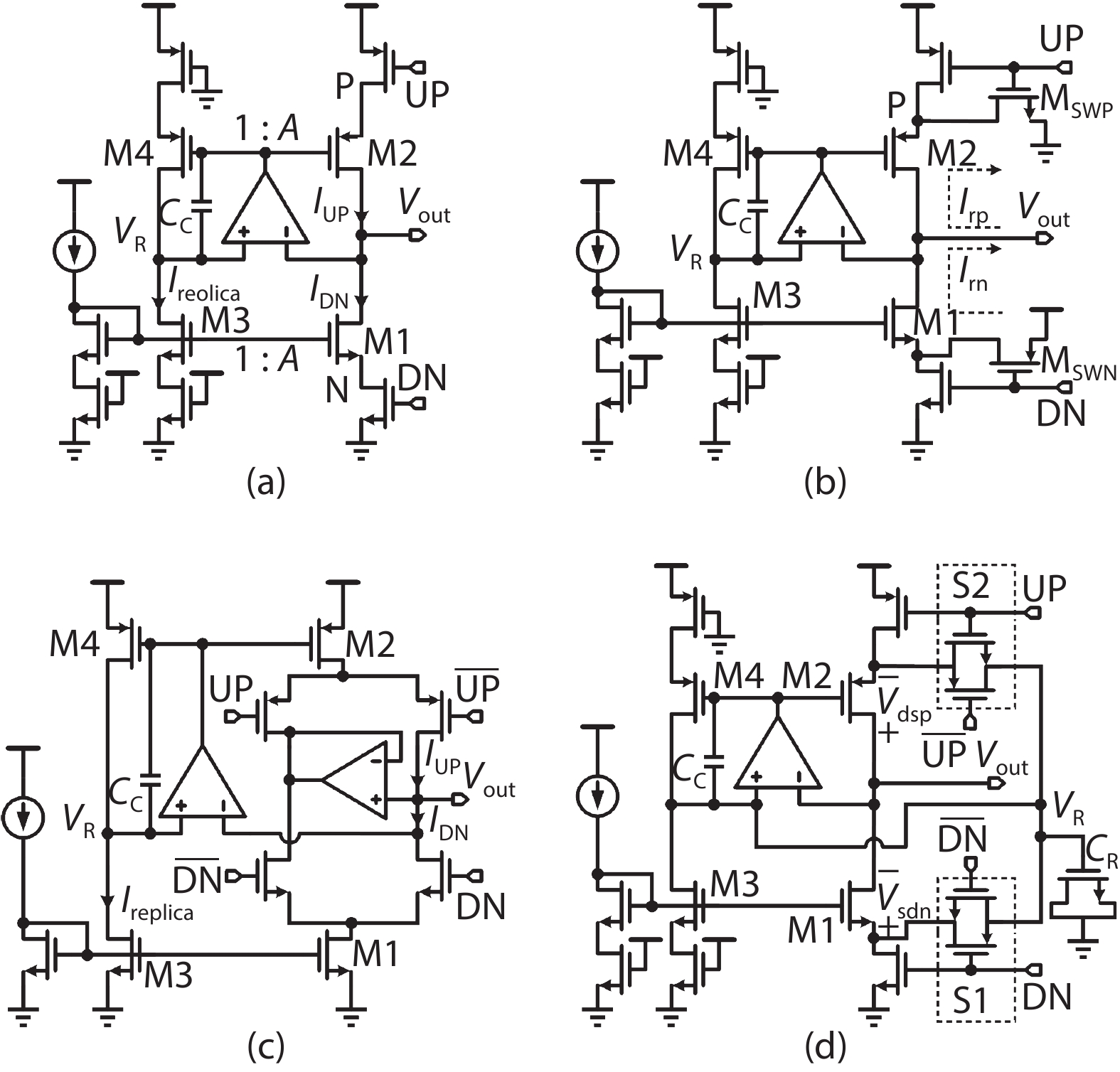
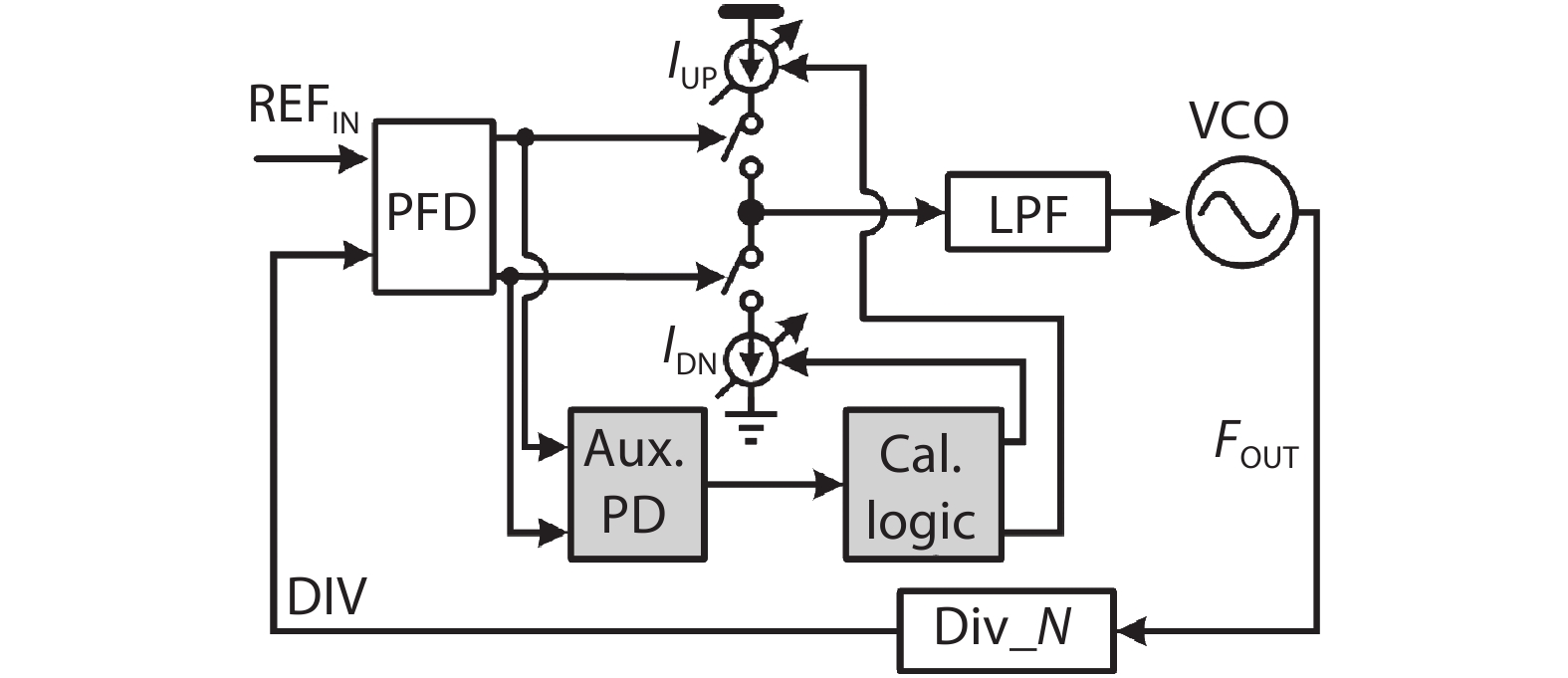
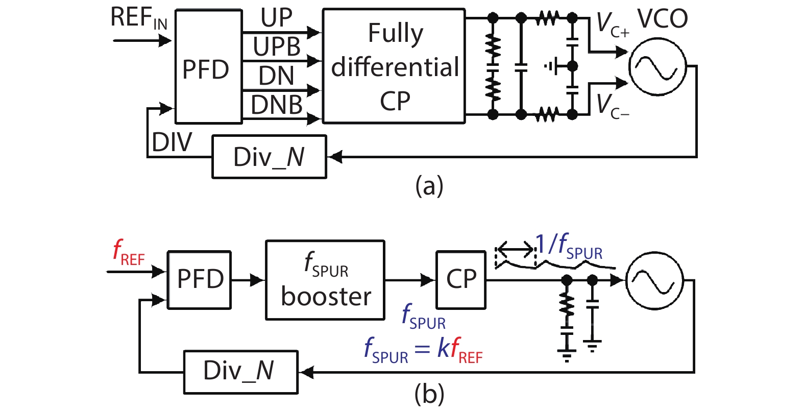
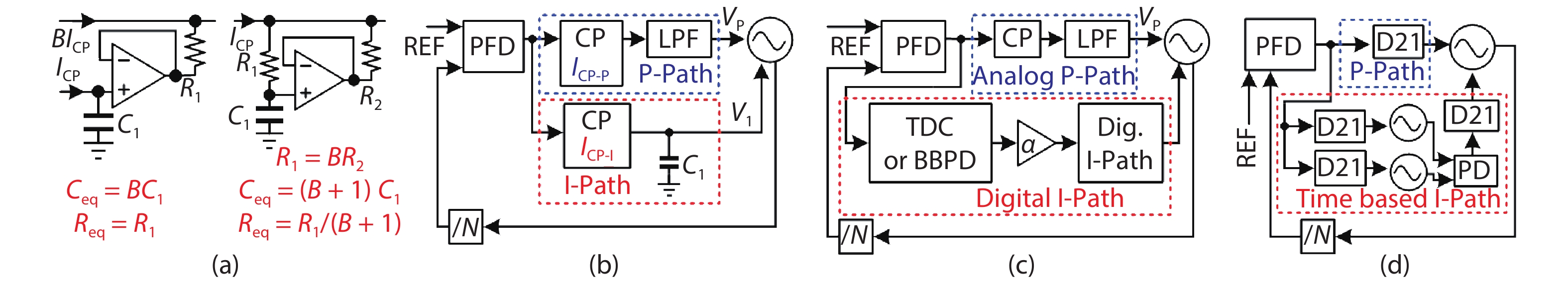
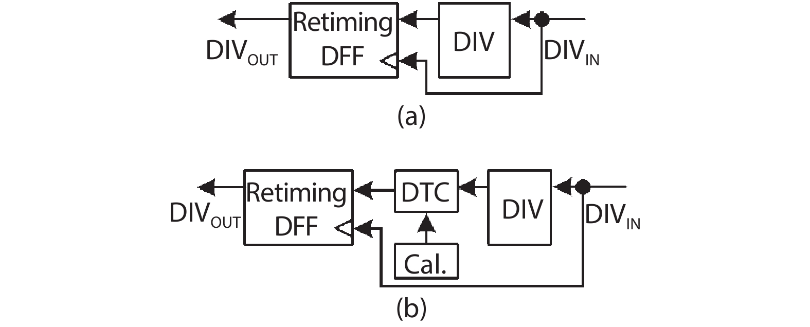
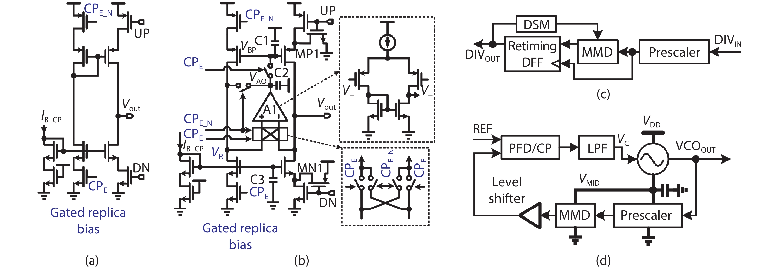
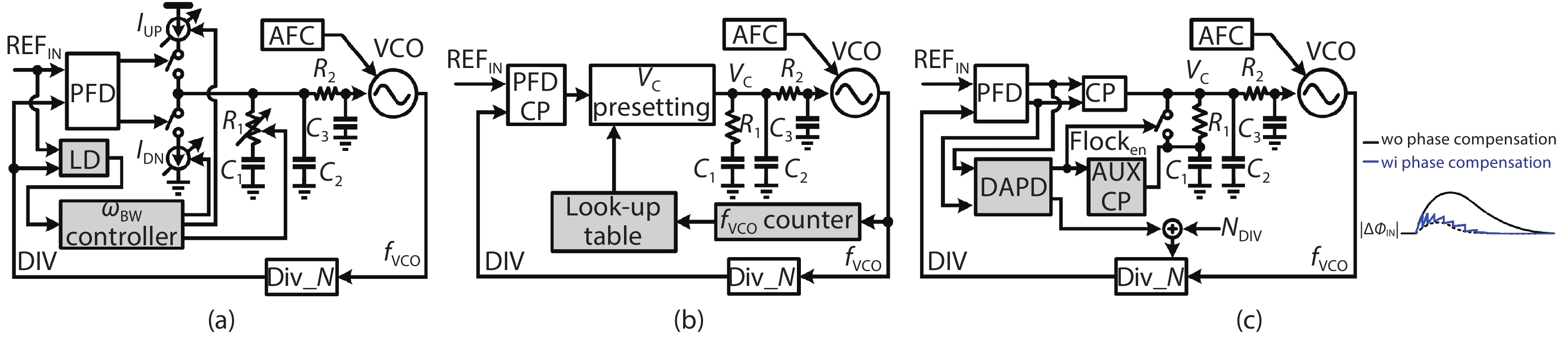
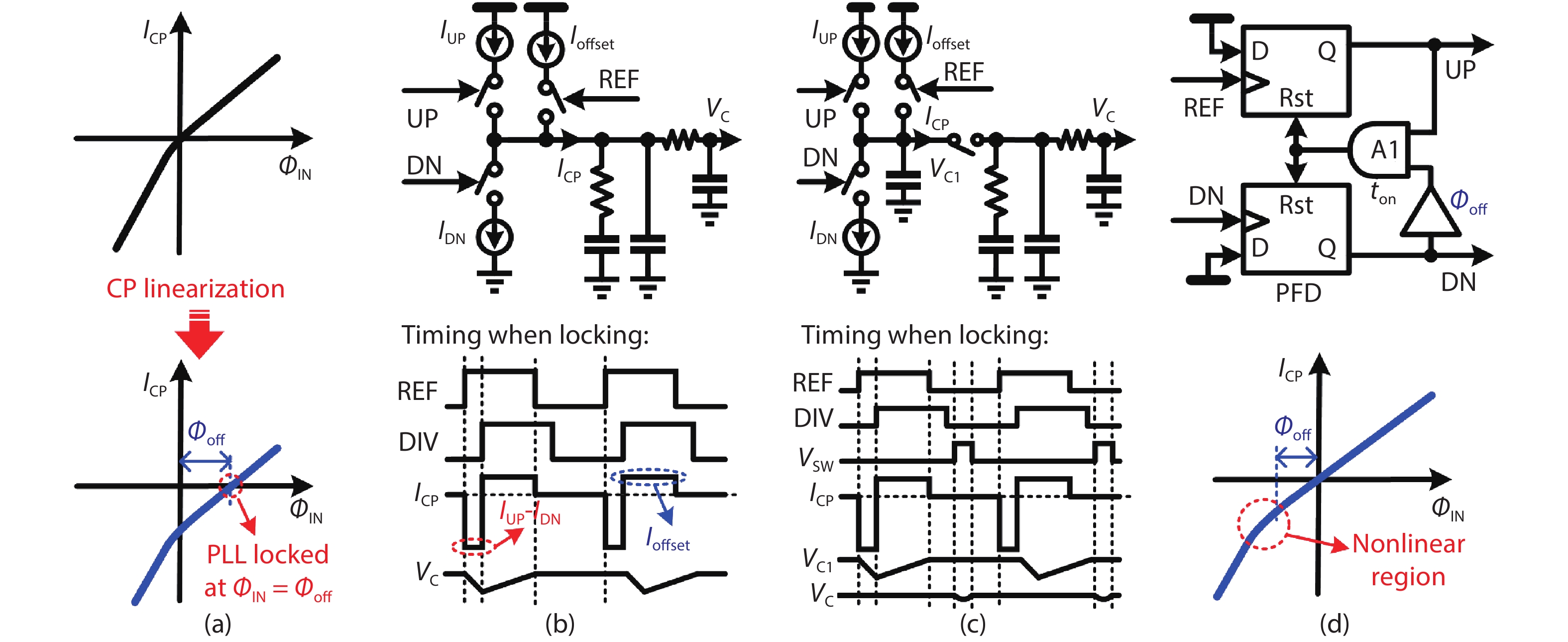
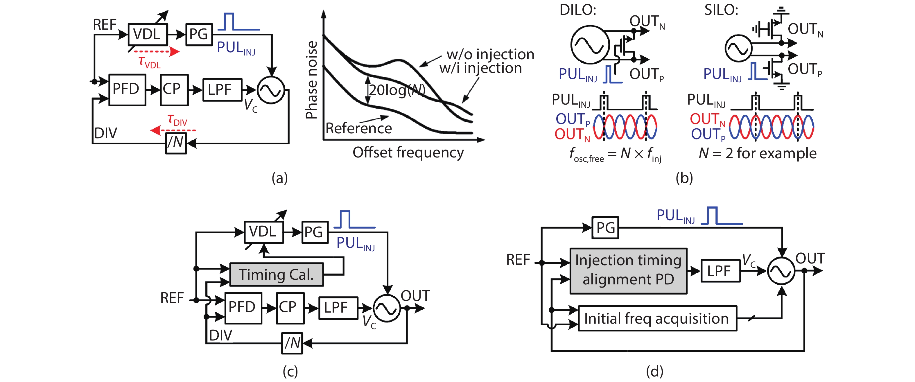
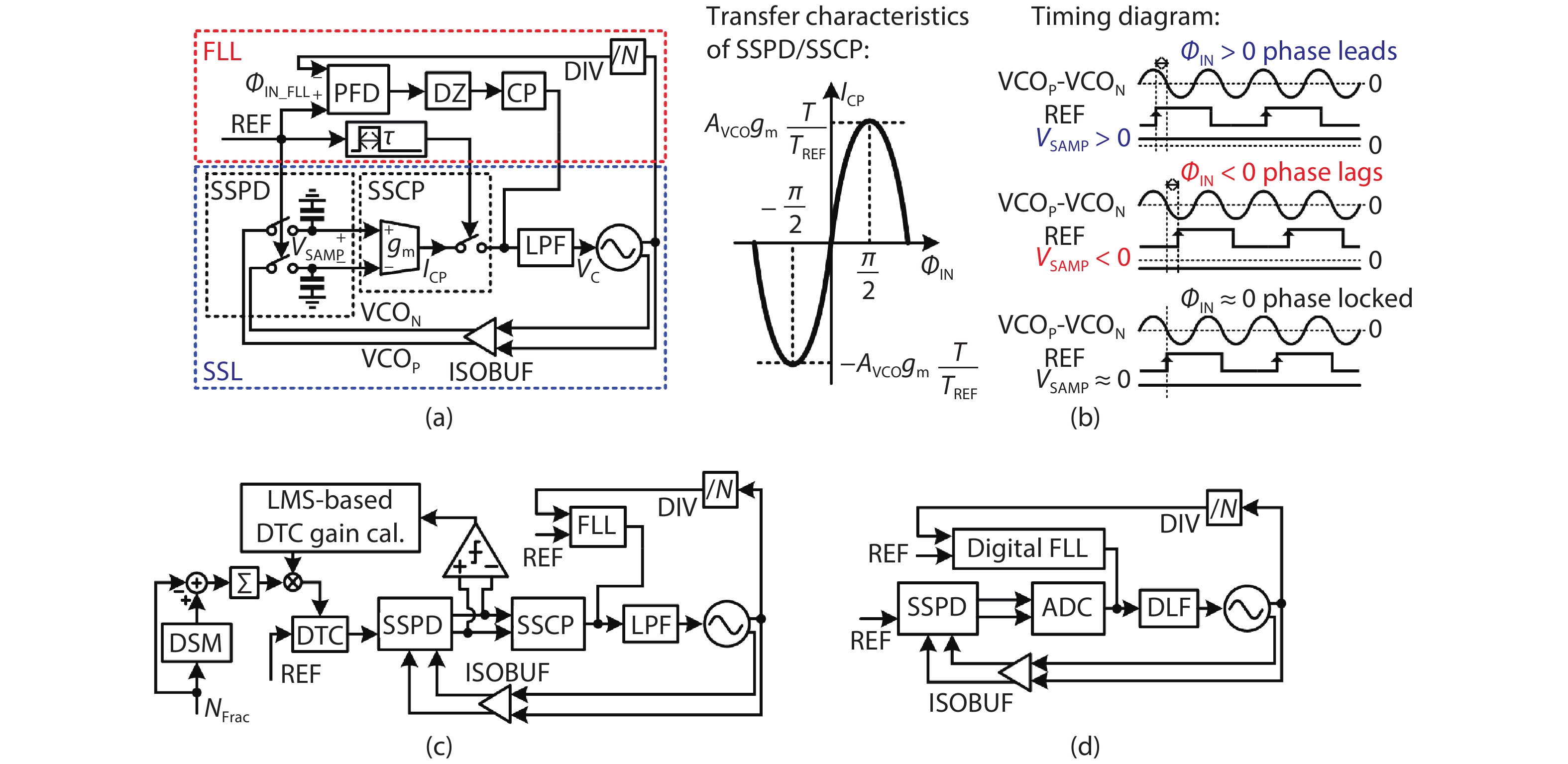
CMOS analog and mixed-signal phase-locked loops (PLL) are widely used in varies of the system-on-chips (SoC) as the clock generator or frequency synthesizer. This paper presents an overview of the AMS-PLL, including: 1) a brief introduction of the basics of the charge-pump based PLL, which is the most widely used AMS-PLL architecture due to its simplicity and robustness; 2) a summary of the design issues of the basic CPPLL architecture; 3) a systematic introduction of the techniques for the performance enhancement of the CPPLL; 4) a brief overview of ultra-low-jitter AMS-PLL architectures which can achieve lower jitter (< 100 fs) with lower power consumption compared with the CPPLL, including the injection-locked PLL (ILPLL), sub-sampling (SSPLL) and sampling PLL (SPLL); 5) a discussion about the consideration of the AMS-PLL architecture selection, which could help designers meet their performance requirements.


J. Semicond.
2020, 41(11): 111403 doi: 10.1088/1674-4926/41/11/111403
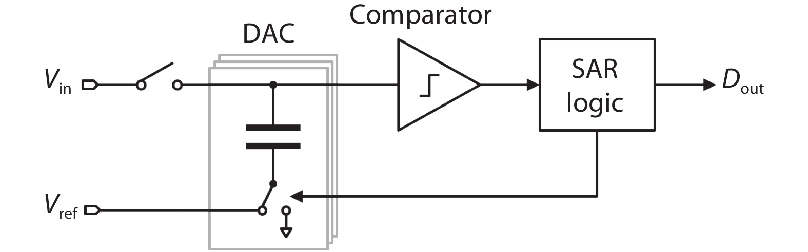
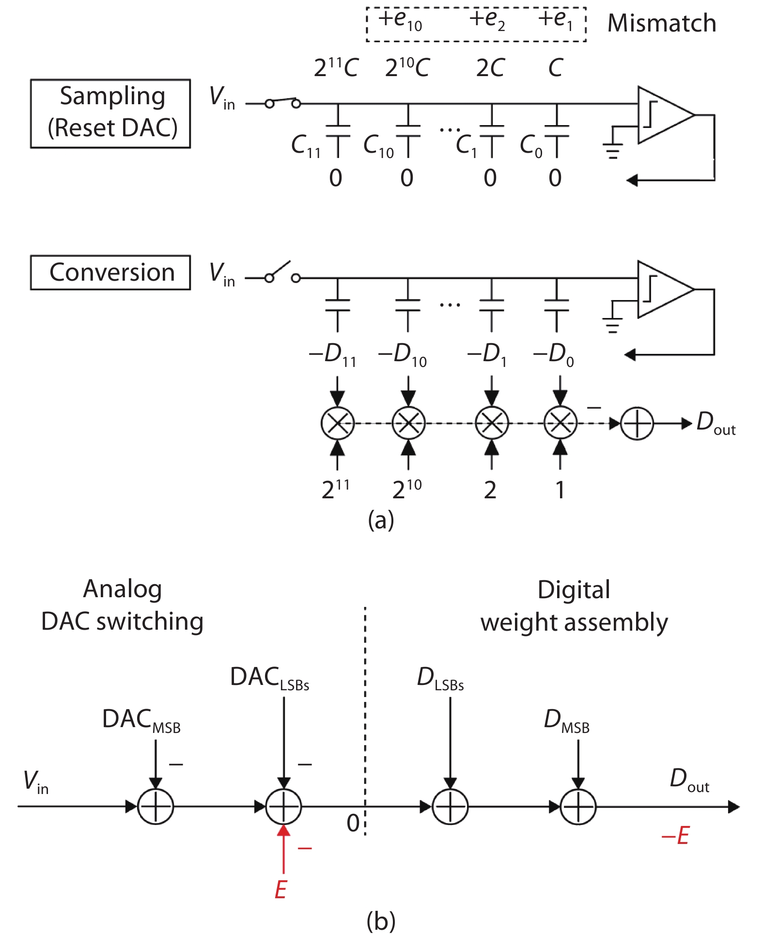
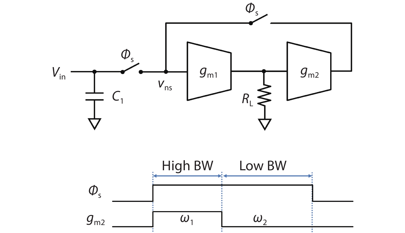
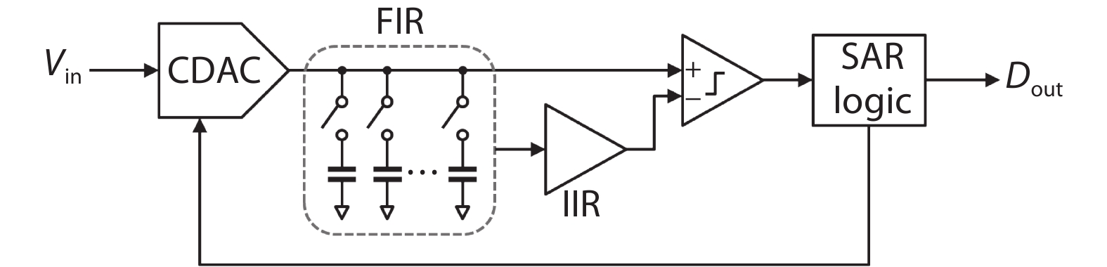
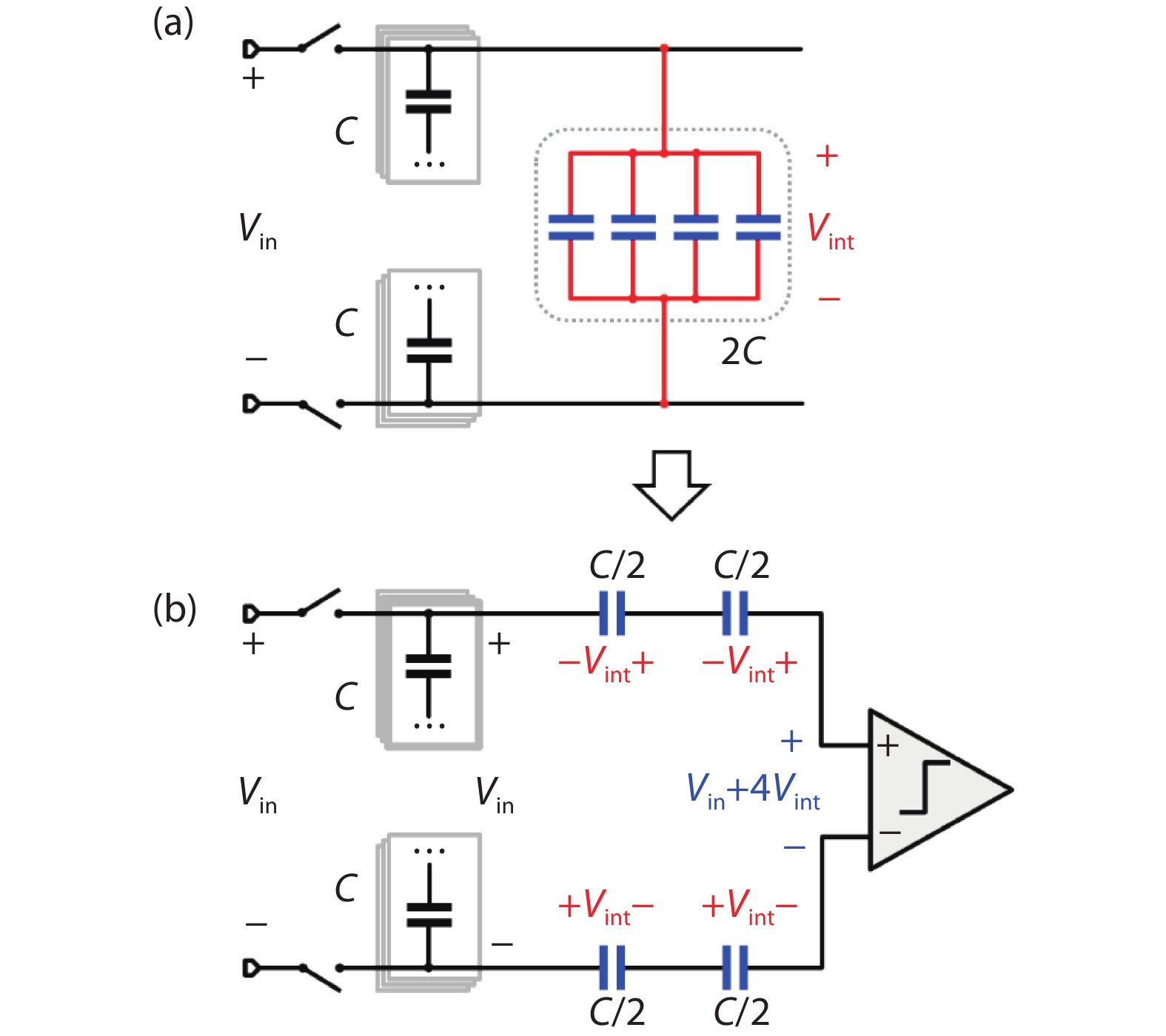
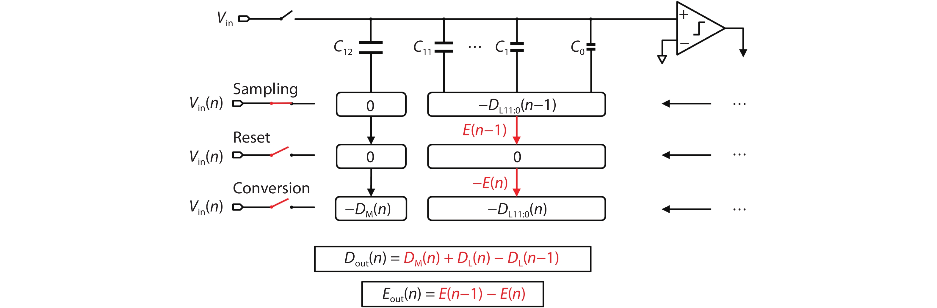
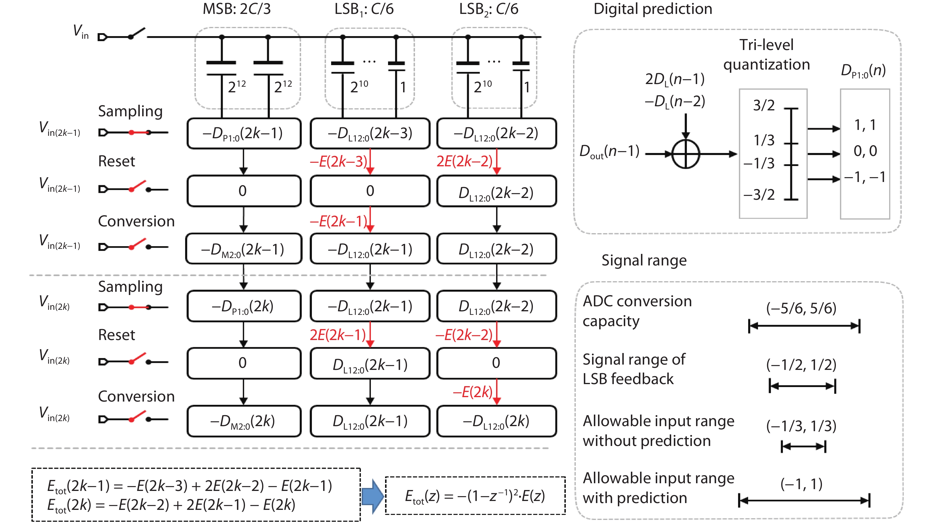
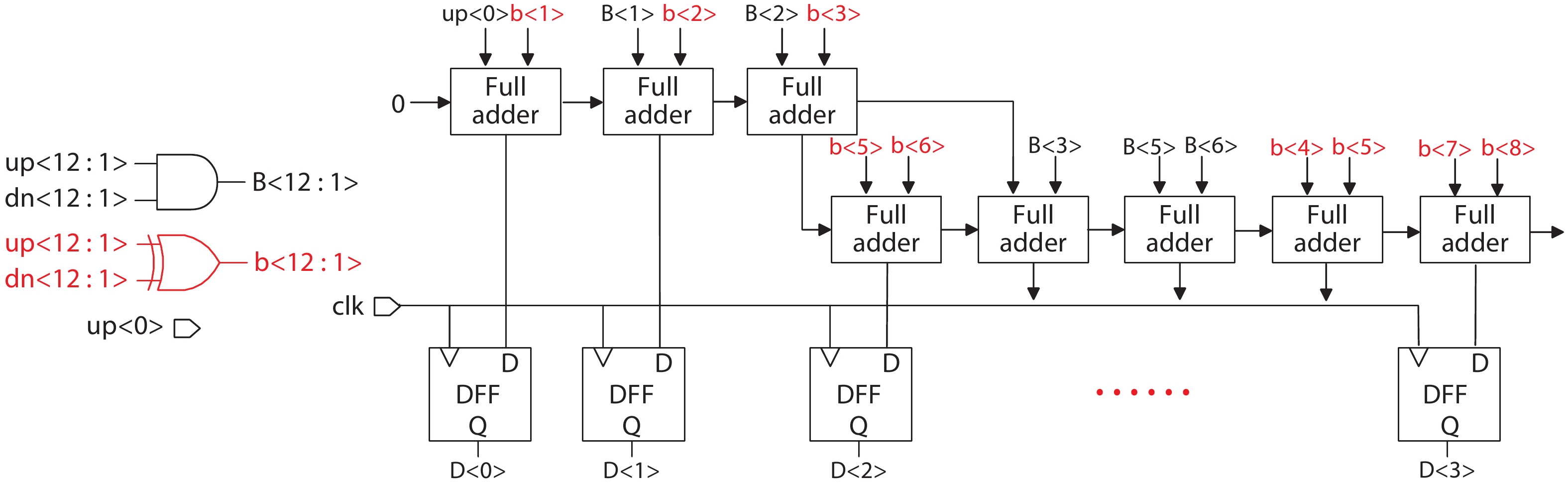
The successive approximation register (SAR) is one of the most energy-efficient analog-to-digital converter (ADC) architecture for medium-resolution applications. However, its high energy efficiency quickly diminishes when the target resolution increases. This is because a SAR ADC suffers from several major error source, including the sampling kT/C noise, the comparator noise, and the DAC mismatch. These errors are increasing hard to address in high-resolution SAR ADCs. This paper reviews recent advances on error suppression techniques for SAR ADCs, including the sampling kT/C noise reduction, the noise-shaping (NS) SAR, and the mismatch error shaping (MES). These techniques aim to boost the resolution of SAR ADCs while maintaining their superior energy efficiency.


J. Semicond.
2020, 41(11): 111404 doi: 10.1088/1674-4926/41/11/111404
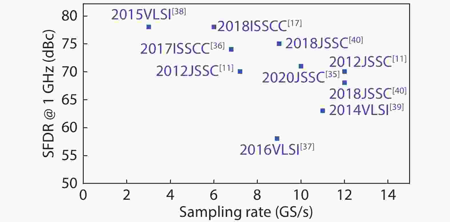
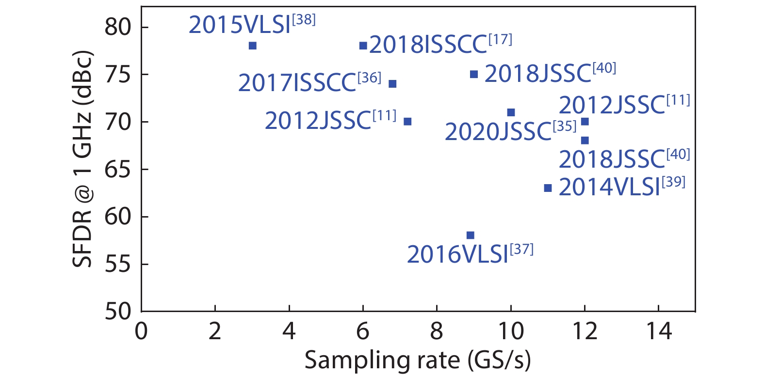
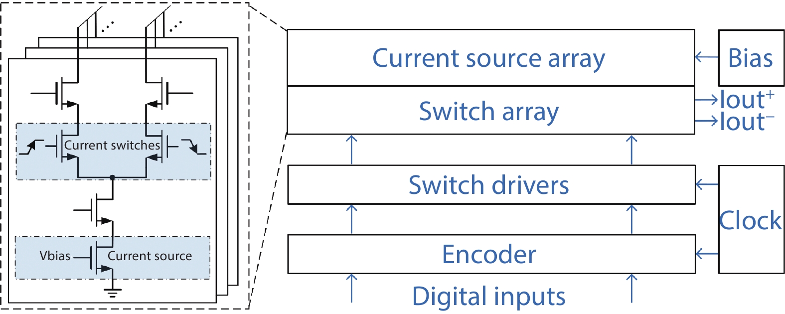
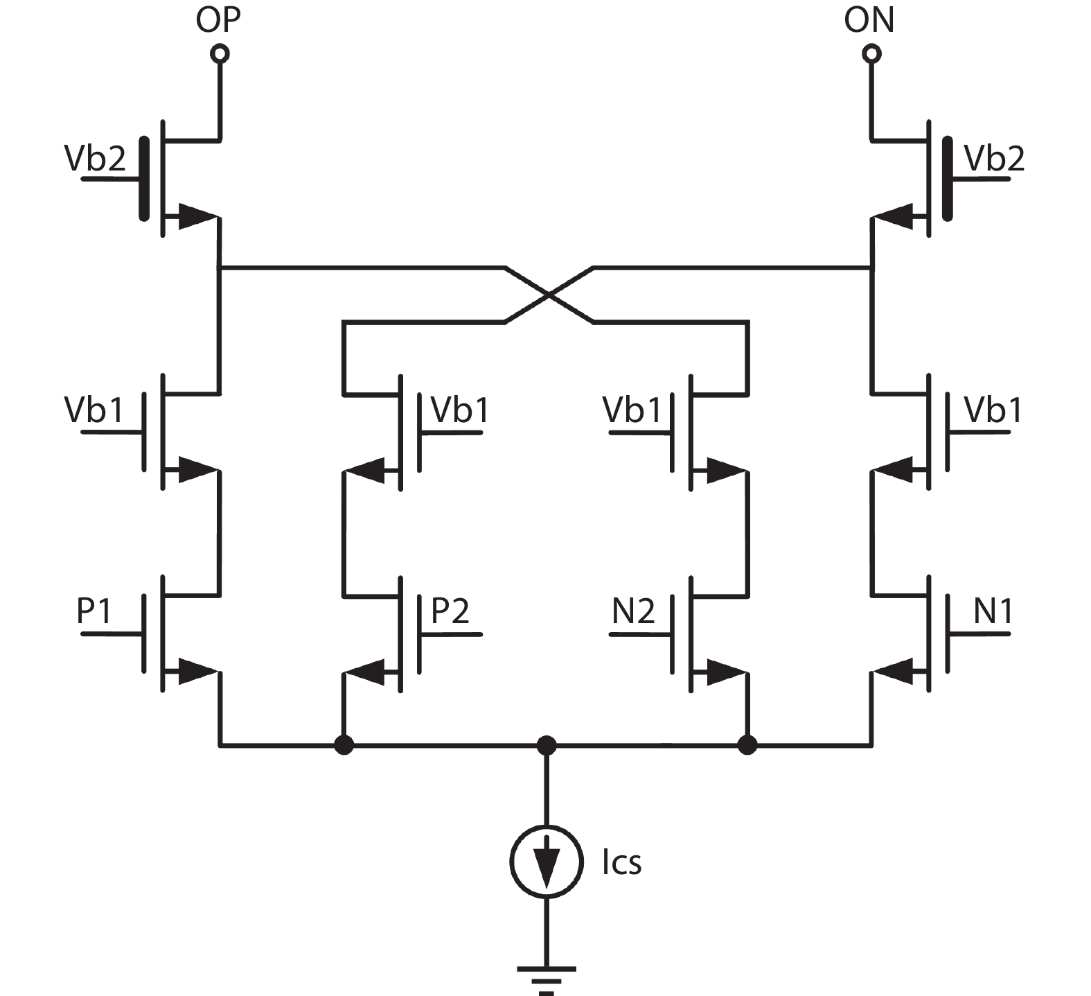
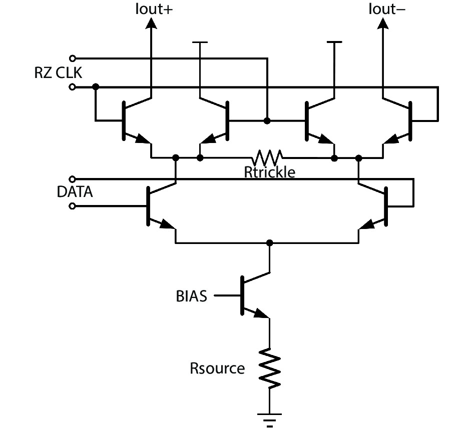
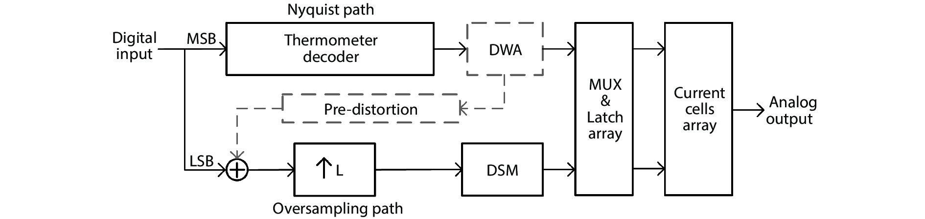
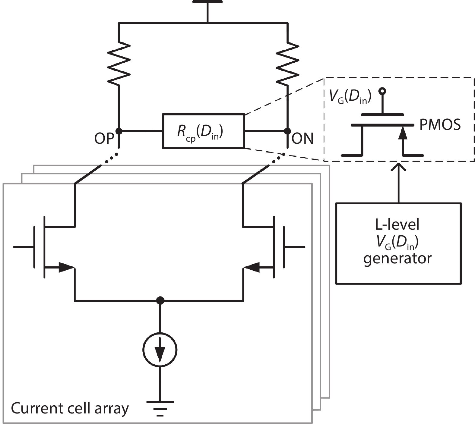
Digital to analog converters (DAC) play an important role as a bridge connecting the analog world and the digital world. With the rapid development of wireless communication, wideband digital radar, and other emerging technologies, better performing high-speed high-resolution DACs are required. In those applications, signal bandwidth and high-frequency linearity often limited by data converters are the bottleneck of the system. This article reviews the state-of-the-art technologies of high-speed and high-resolution DACs reported in recent years. Comparisons are made between different architectures, circuit implementations and calibration techniques along with the figure of merit (FoM) results.


J. Semicond.
2020, 41(11): 111405 doi: 10.1088/1674-4926/41/11/111405

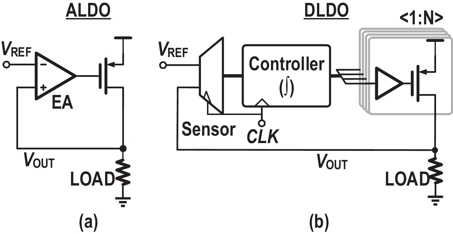
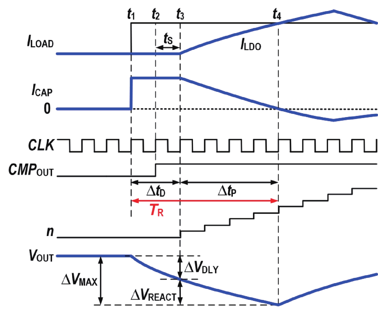
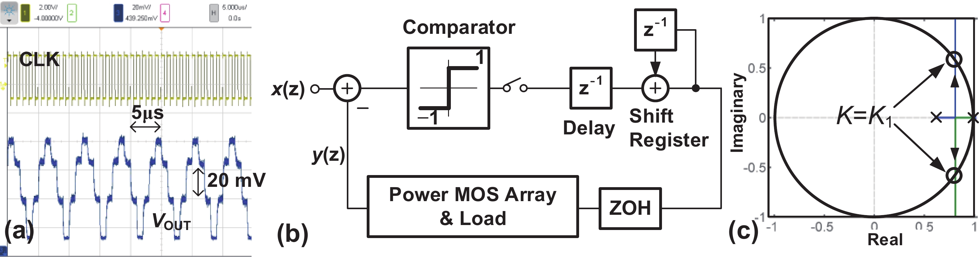
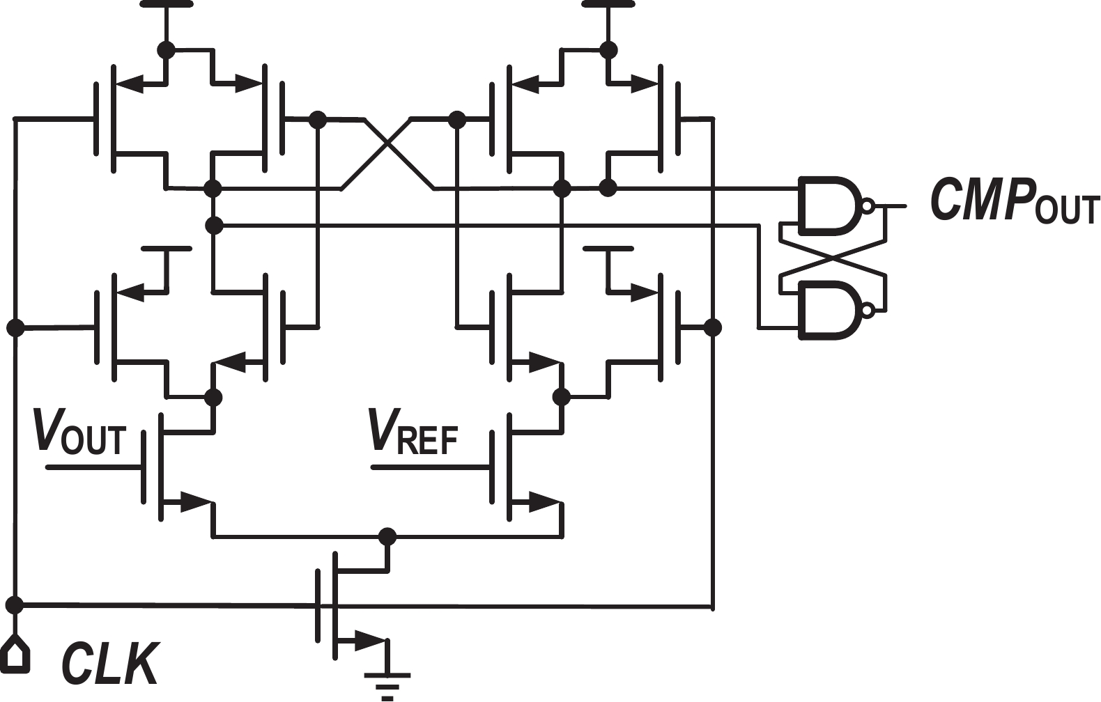
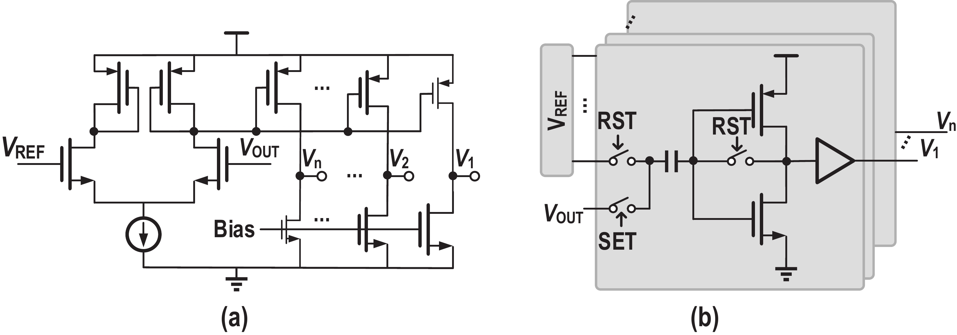
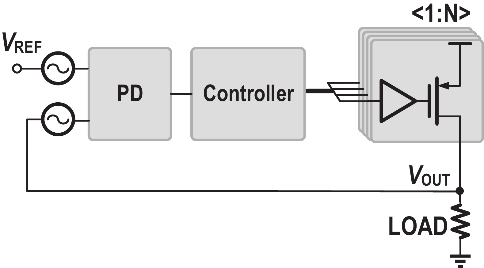
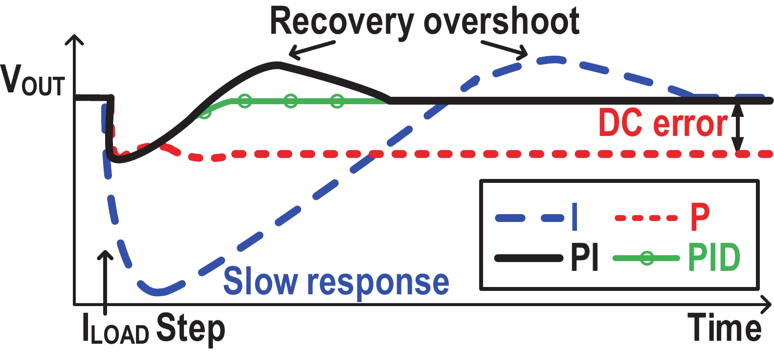
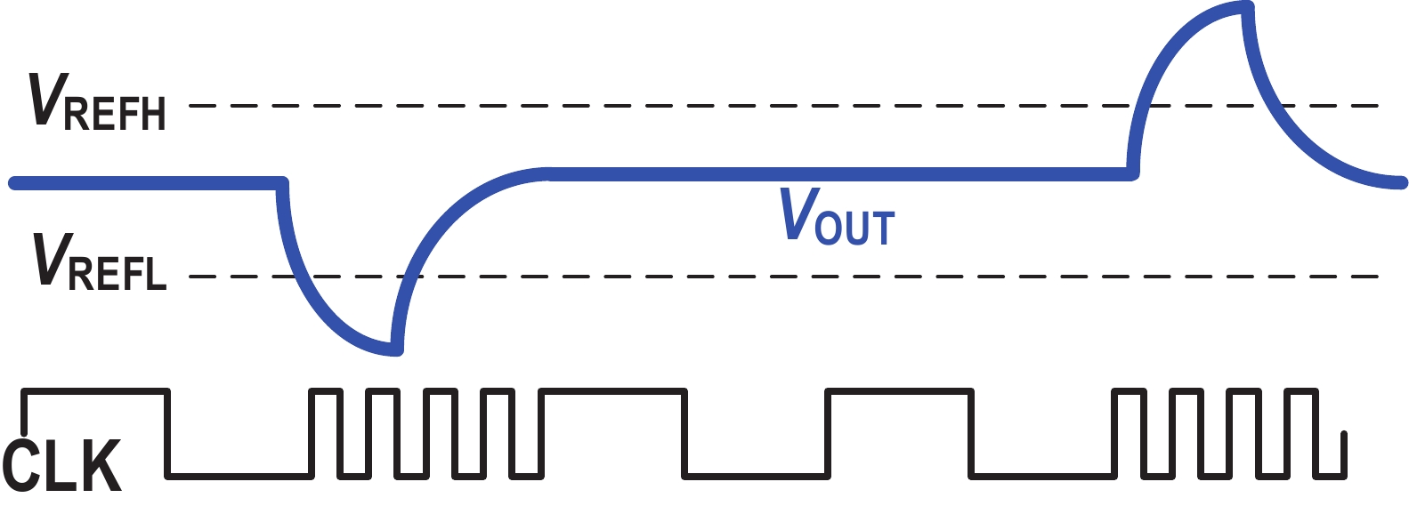
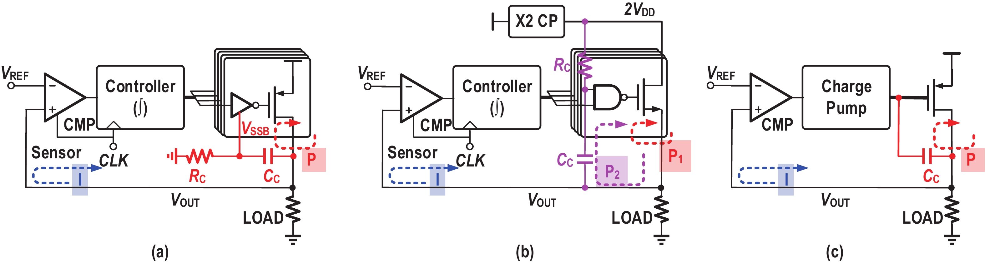
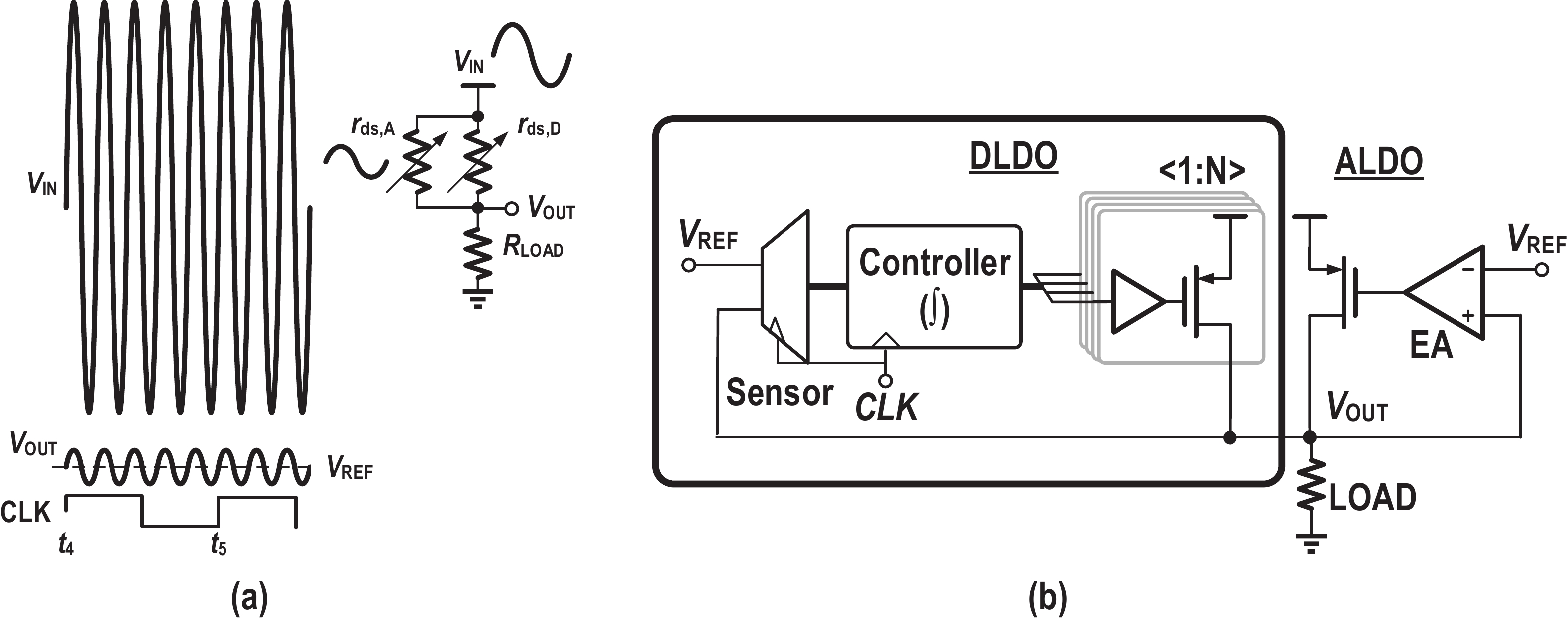
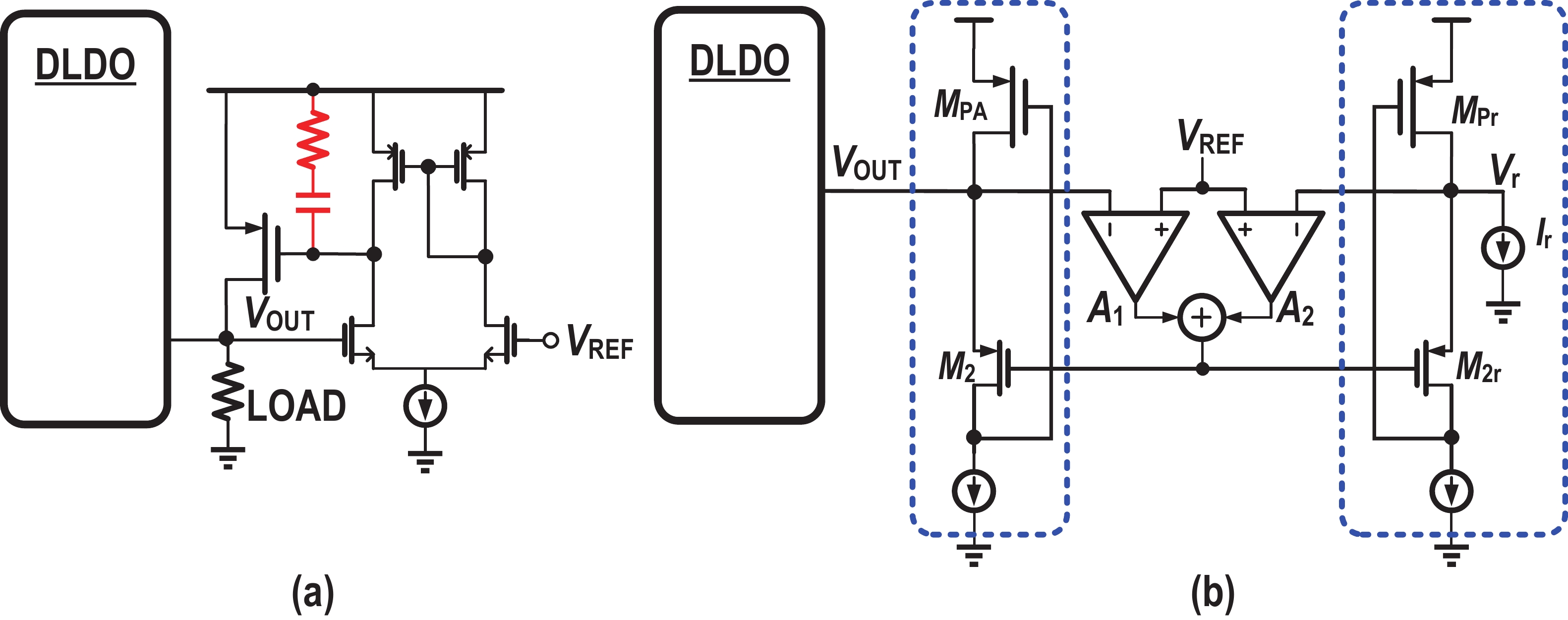
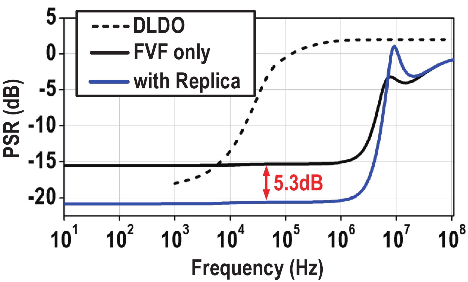
Granular power management in a power-efficient system on a chip (SoC) requires multiple integrated voltage regulators with a small area, process scalability, and low supply voltage. Conventional on-chip analog low-dropout regulators (ALDOs) can hardly meet these requirements, while digital LDOs (DLDOs) are good alternatives. However, the conventional DLDO, with synchronous control, has inherently slow transient response limited by the power-speed trade-off. Meanwhile, it has a poor power supply rejection (PSR), because the fully turned-on power switches in DLDO are vulnerable to power supply ripples. In this comparative study on DLDOs, first, we compare the pros and cons between ALDO and DLDO in general. Then, we summarize the recent DLDO advanced techniques for fast transient response and PSR enhancement. Finally, we discuss the design trends and possible directions of DLDO.


J. Semicond.
2020, 41(11): 111406 doi: 10.1088/1674-4926/41/11/111406
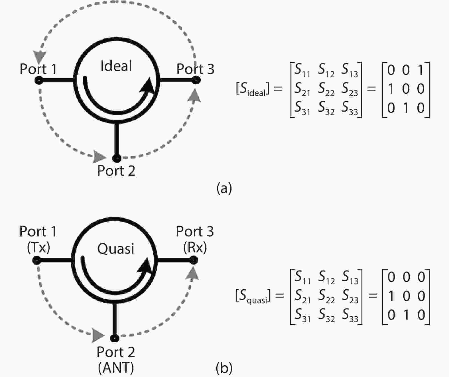
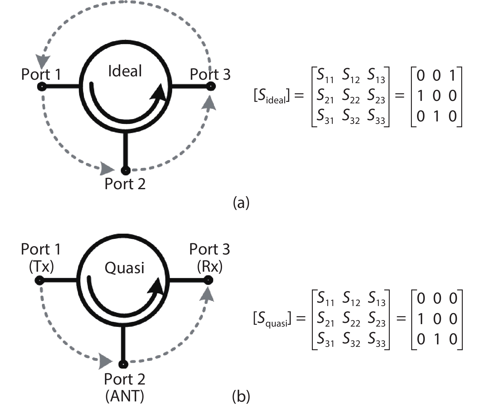
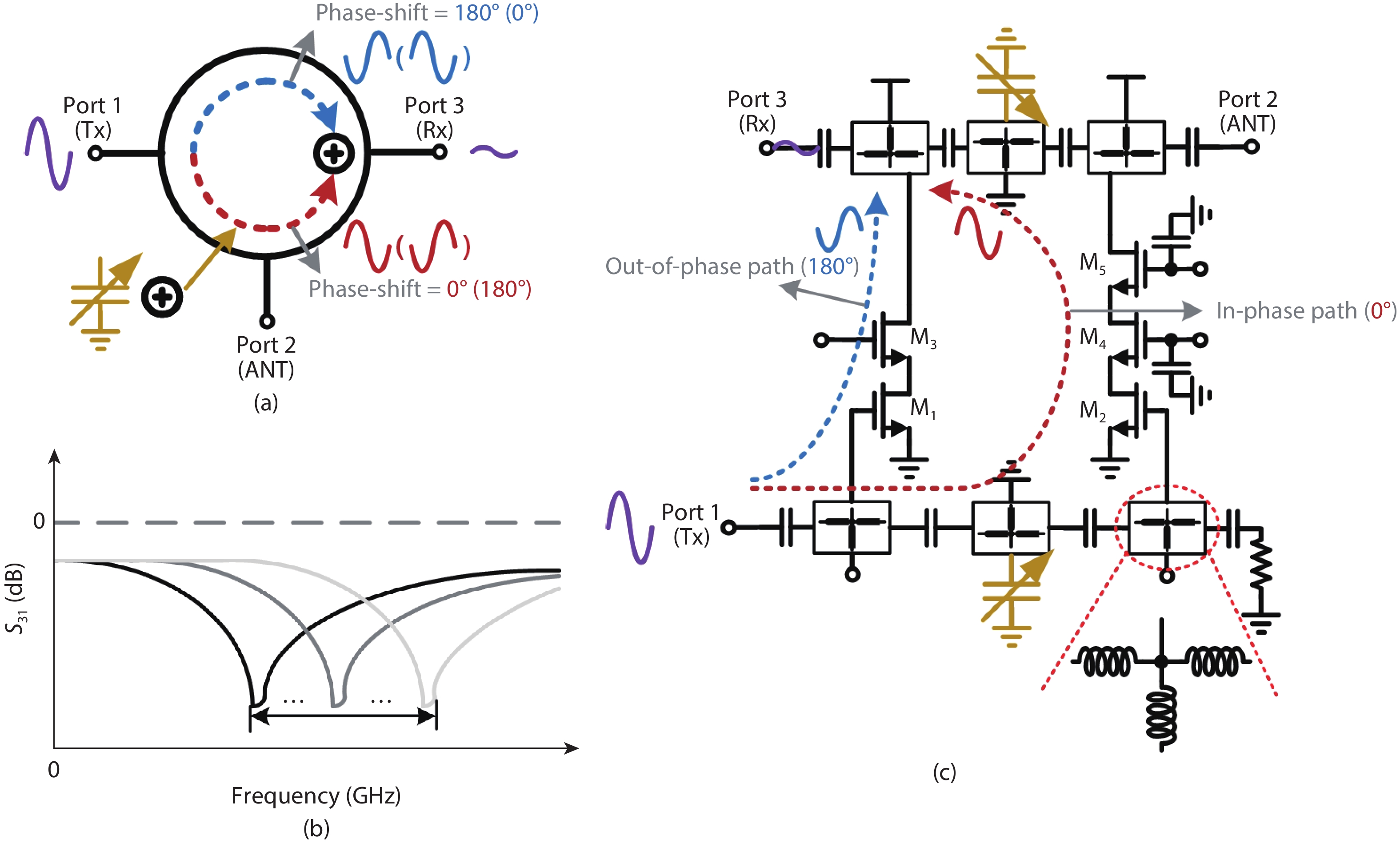
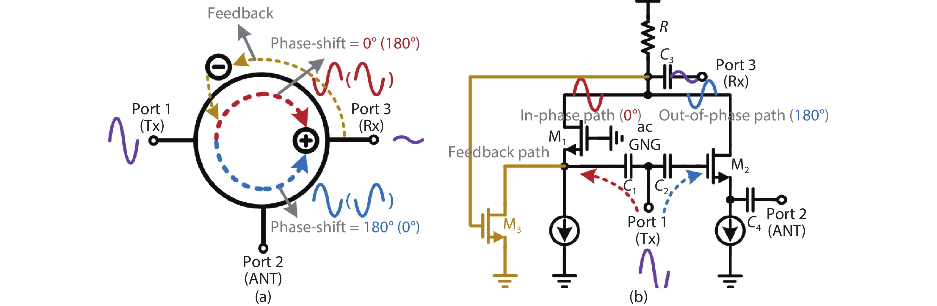
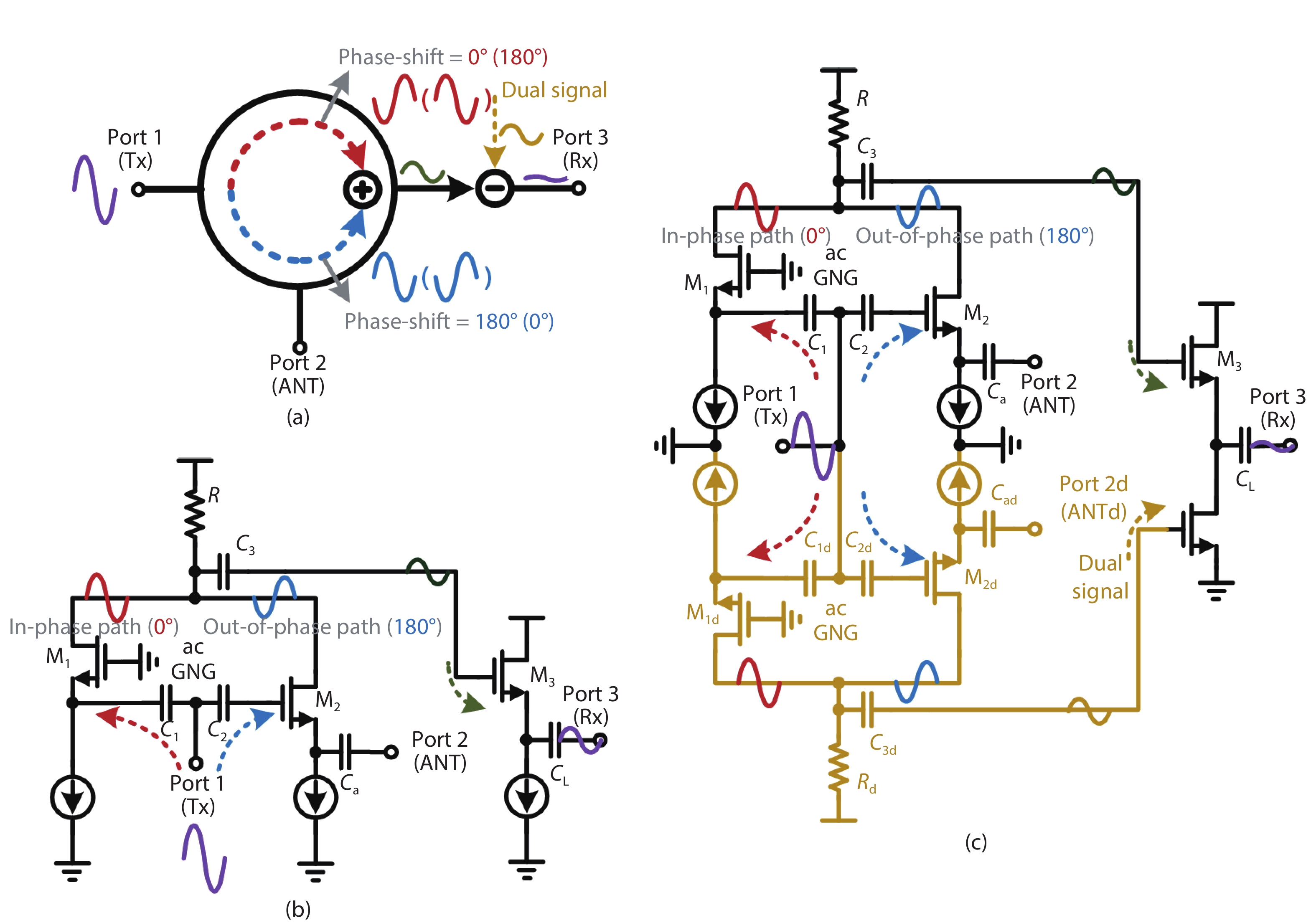
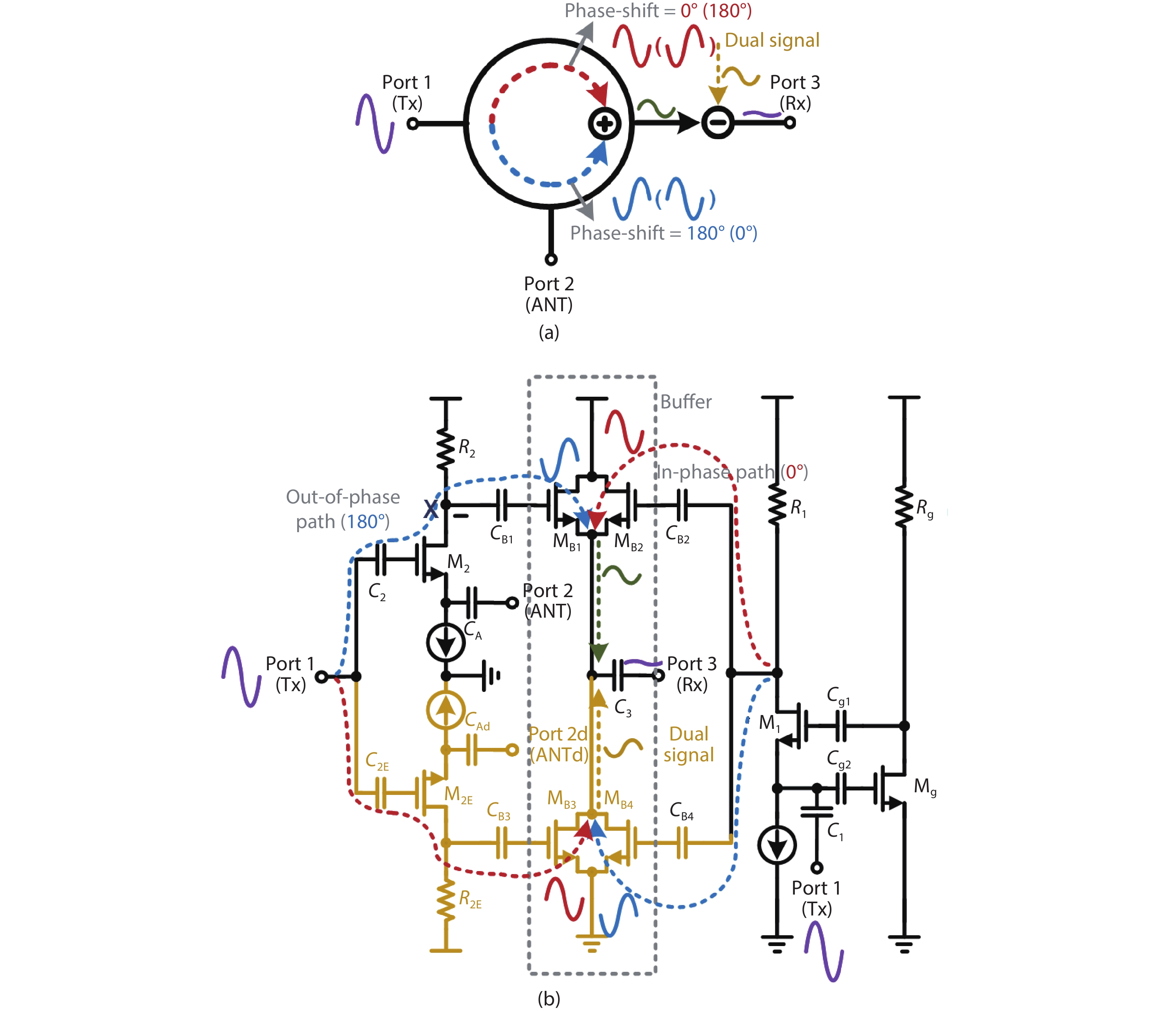
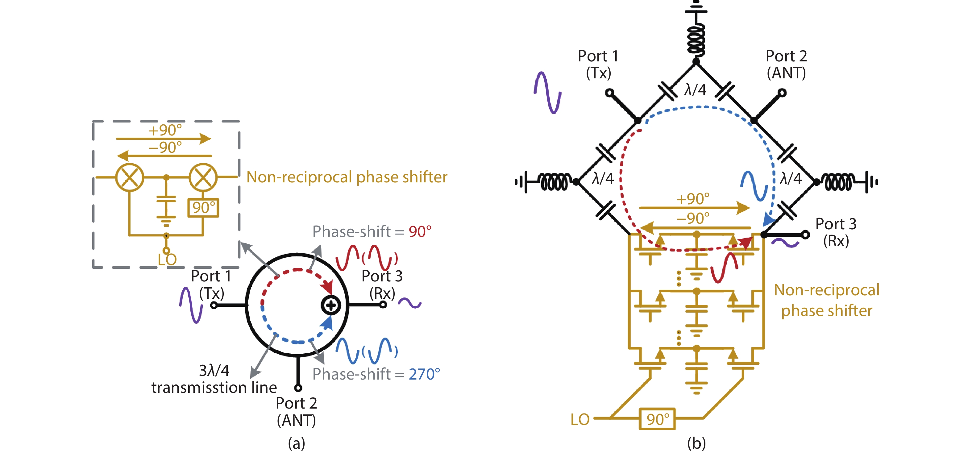
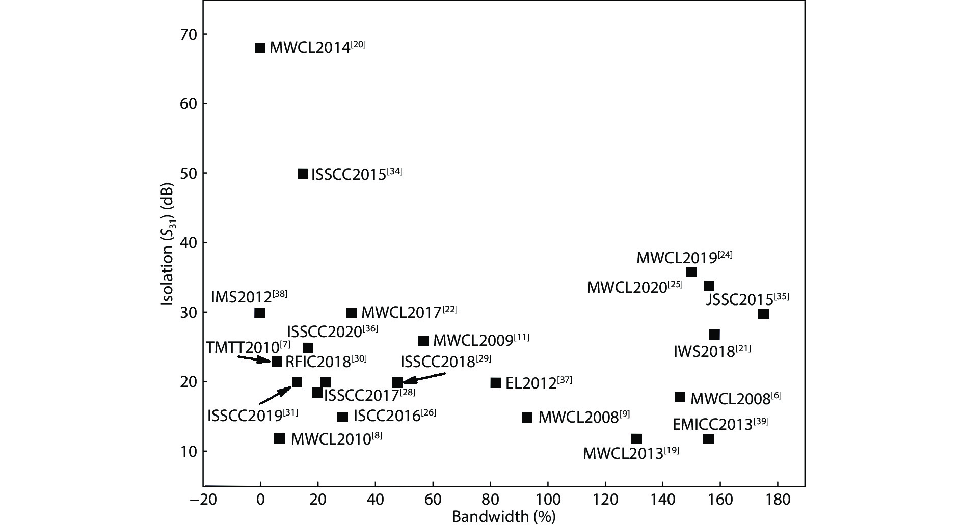
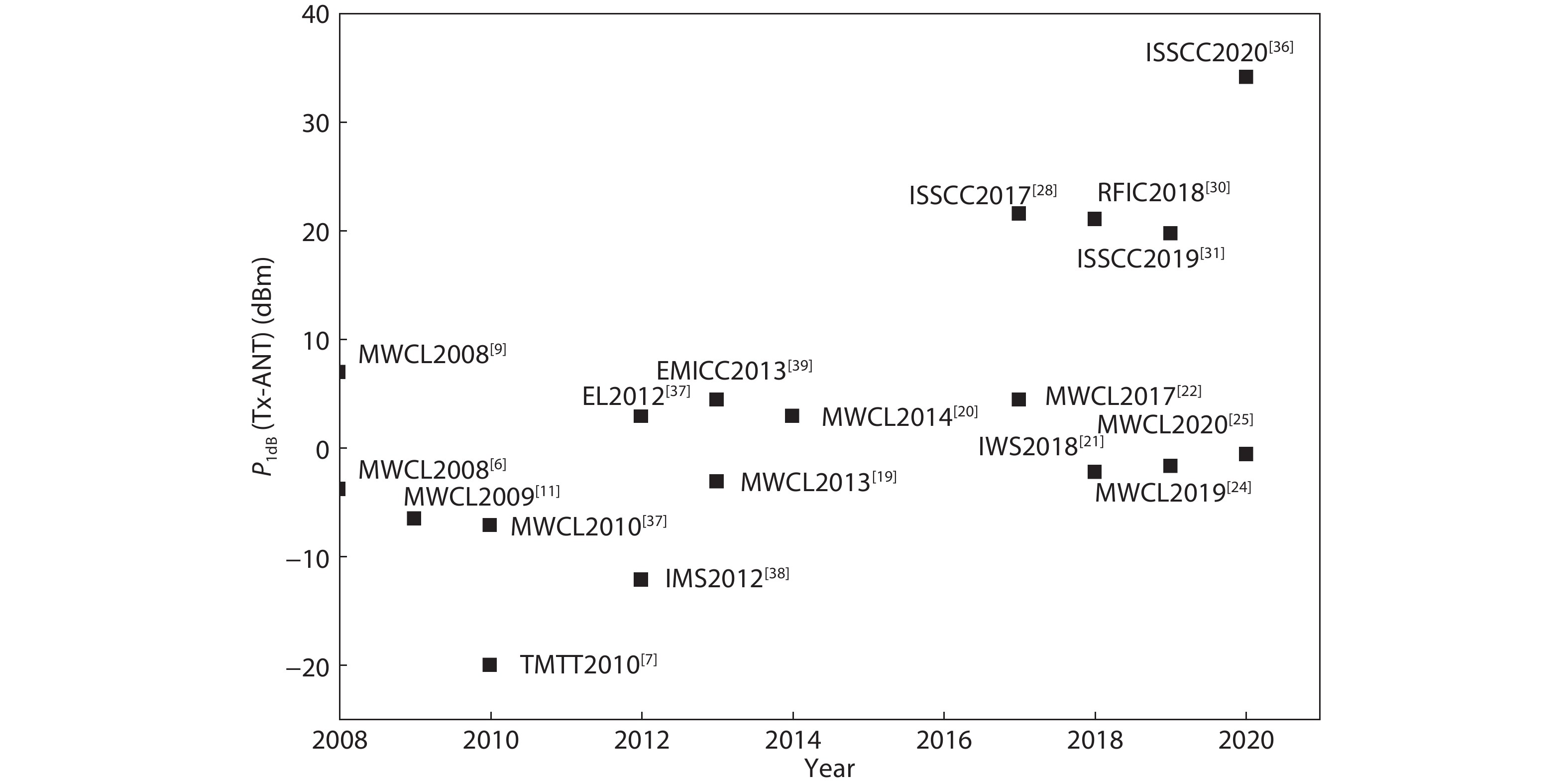
With the development of multi-band wireless communication and the increasing data transmission rate, the circulator as an antenna interface must be able to work in multiple frequency bands and provides large bandwidth. It presents a high challenge to the design of circulators, especially the active quasi-circulators. In this survey, we review the representative active quasi-circulators and summarize three different techniques and the corresponding structures to show an incremental improvement of the isolation and bandwidth of the active quasi-circulators. In addition, we also compare the performance of several state-of-art active circulators, and analyze their advantages and disadvantages. Finally, we conclude the future trend of the active quasi-circulators.

J. Semicond.
2020, 41(11): 111407 doi: 10.1088/1674-4926/41/11/111407

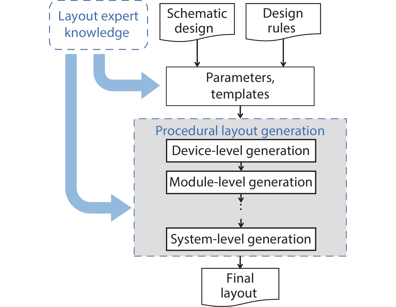
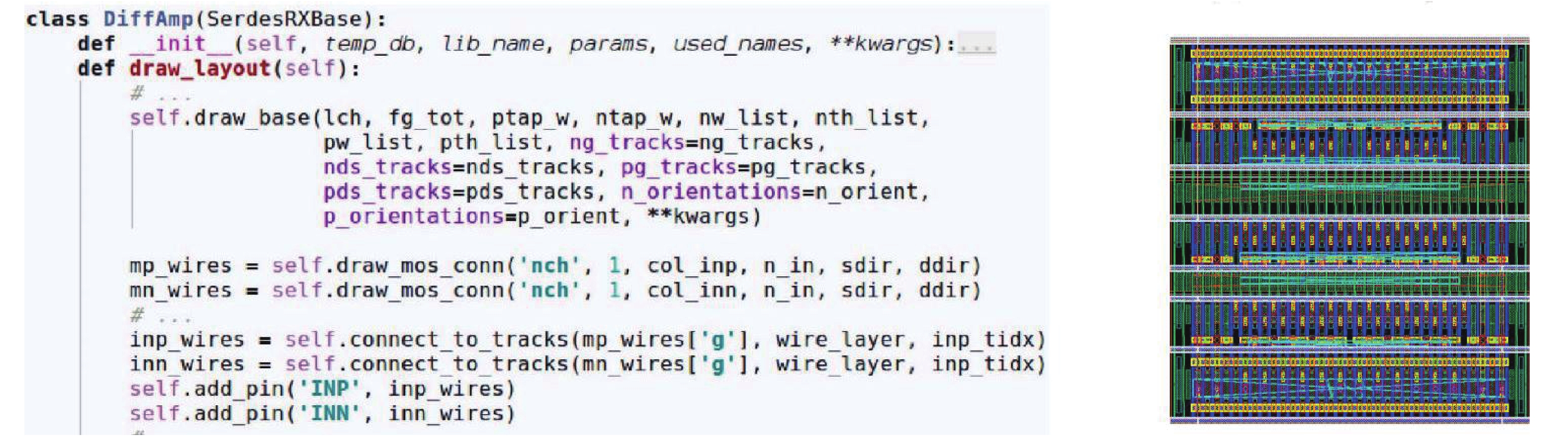
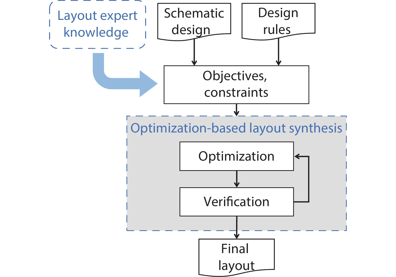
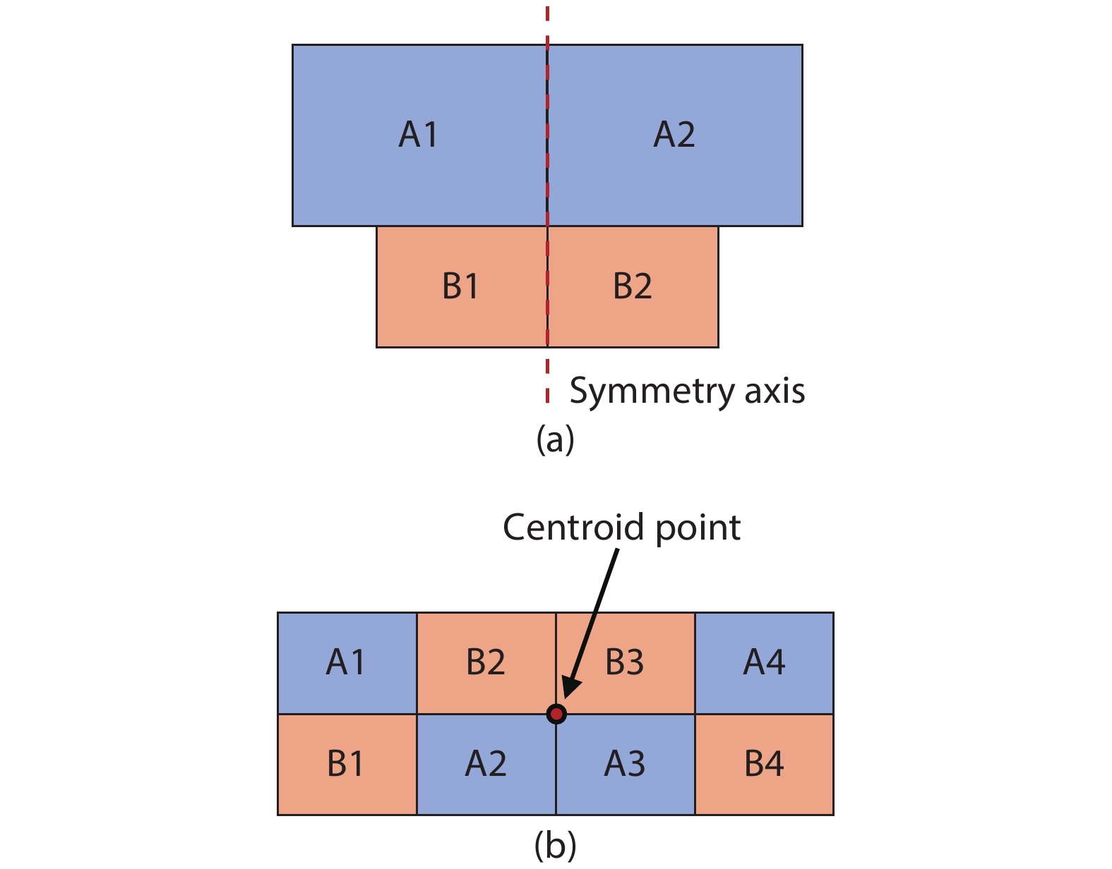
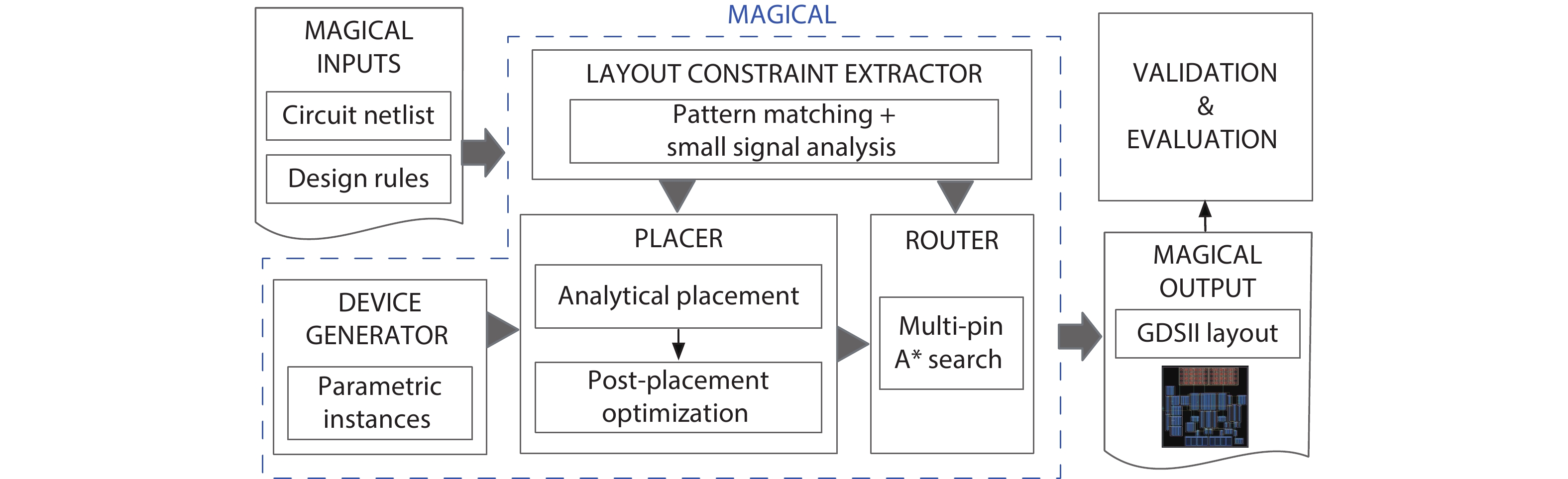
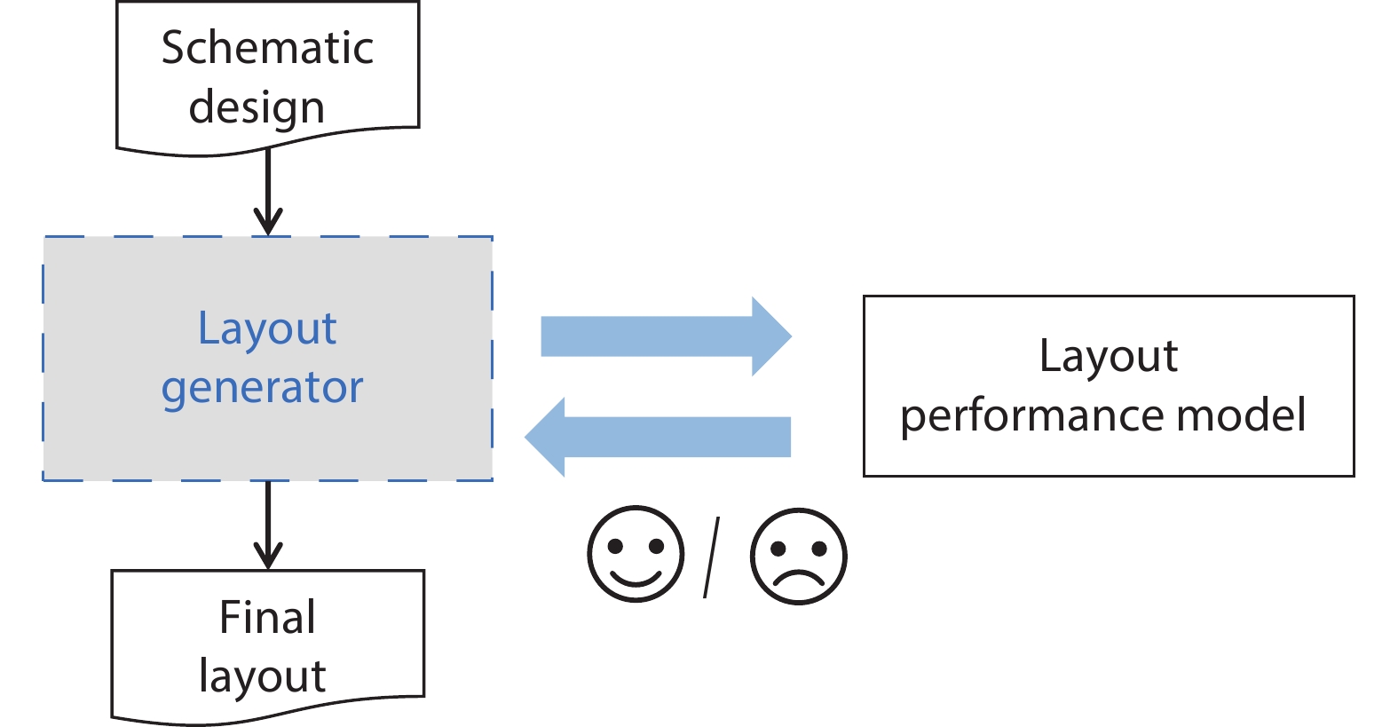
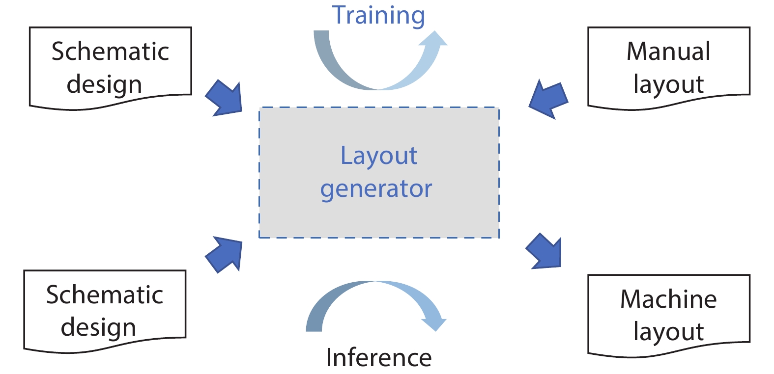
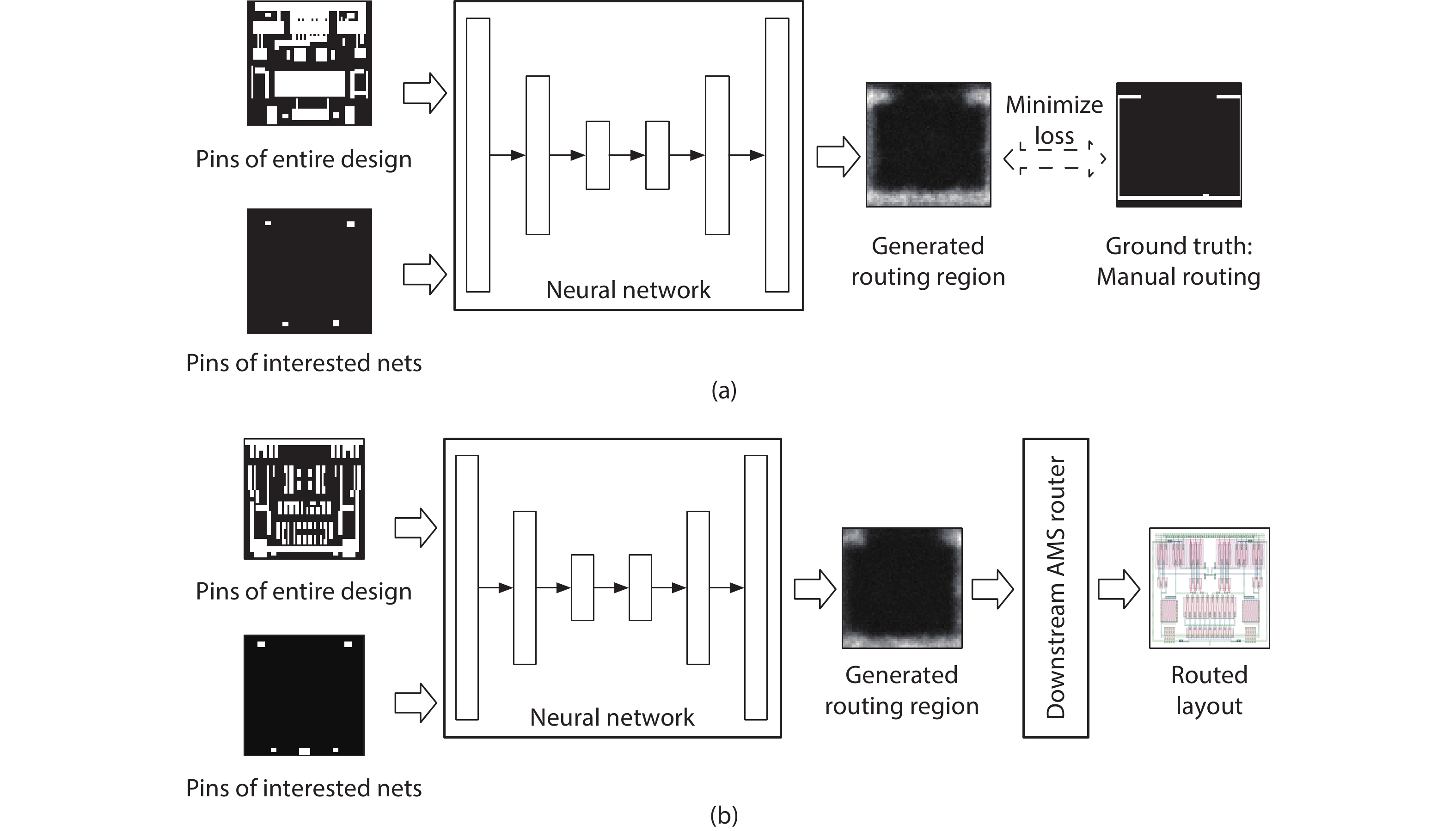
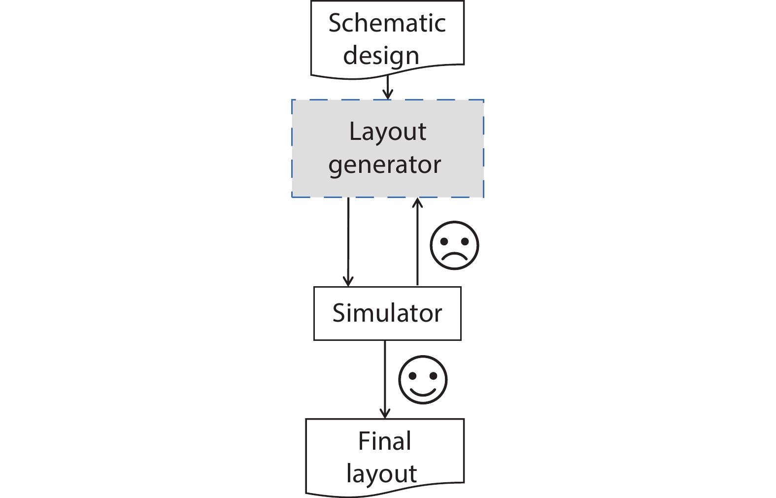
Realizing the layouts of analog/mixed-signal (AMS) integrated circuits (ICs) is a complicated task due to the high design flexibility and sensitive circuit performance. Compared with the advancements of digital IC layout automation, analog IC layout design is still heavily manual, which leads to a more time-consuming and error-prone process. In recent years, significant progress has been made in automated analog layout design with emerging of several open-source frameworks. This paper firstly reviews the existing state-of-the art AMS layout synthesis frameworks with focus on the different approaches and their individual challenges. We then present recent research trends and opportunities in the field. Finally, we summaries the paper with open questions and future directions for fully-automating the analog IC layout.

J. Semicond.
2020, 41(11): 112401 doi: 10.1088/1674-4926/41/11/112401
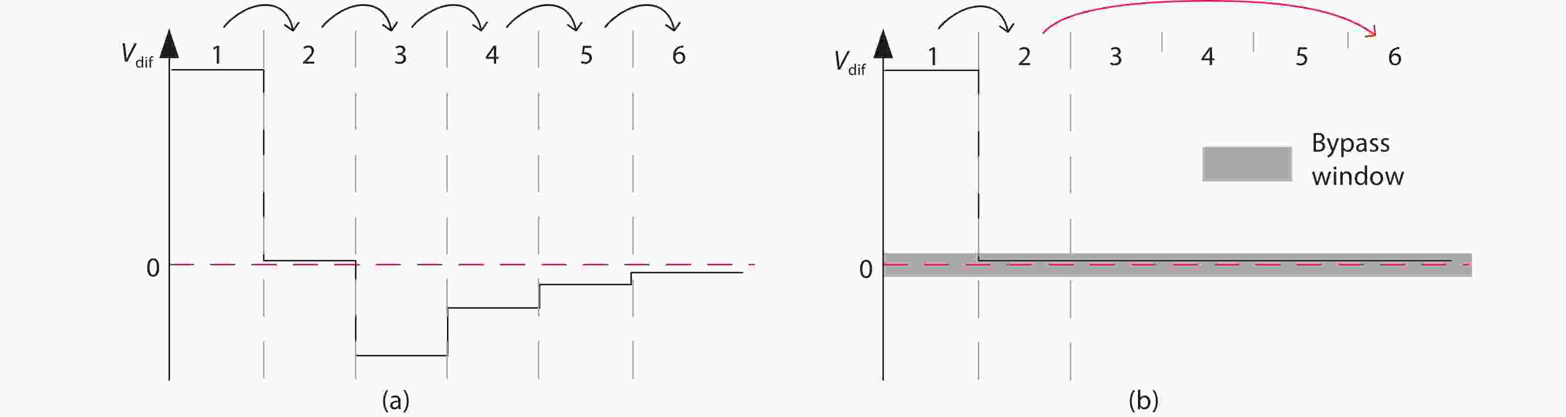
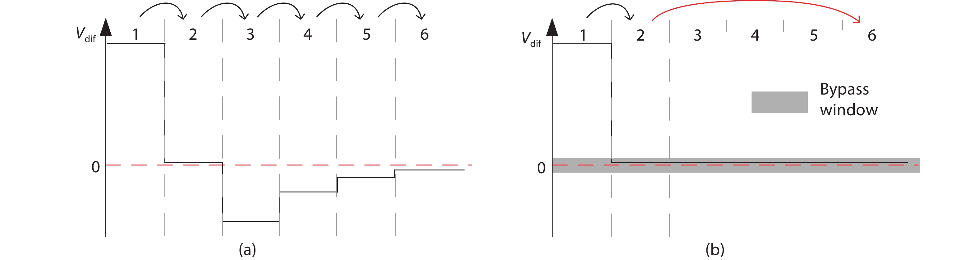
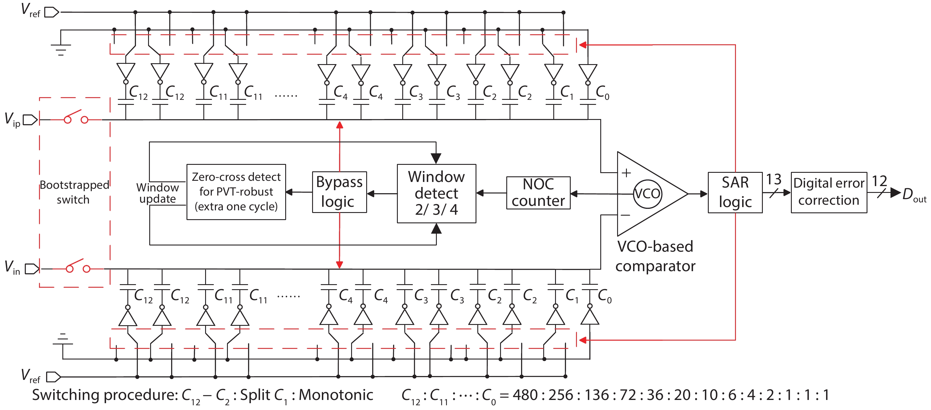
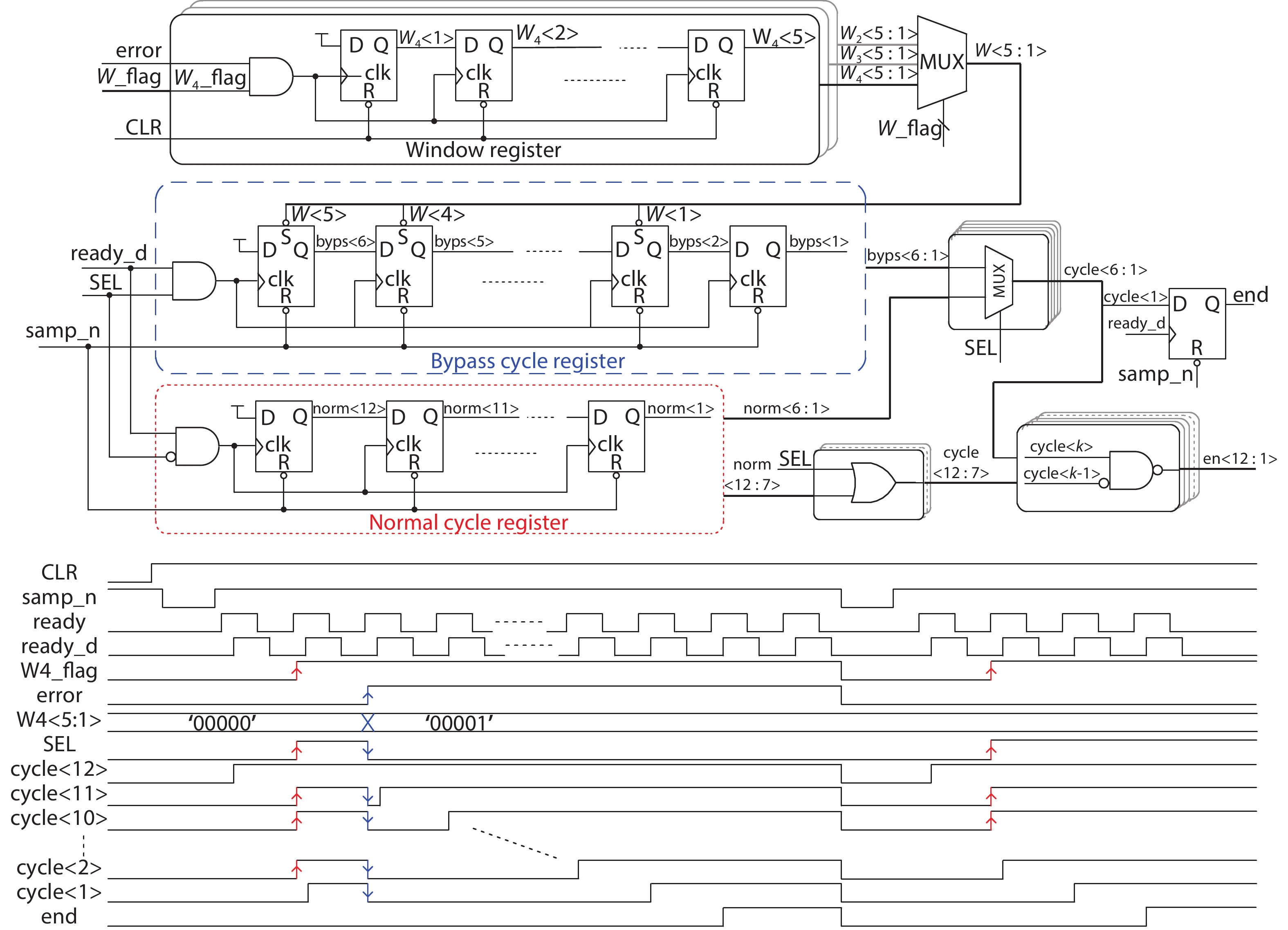
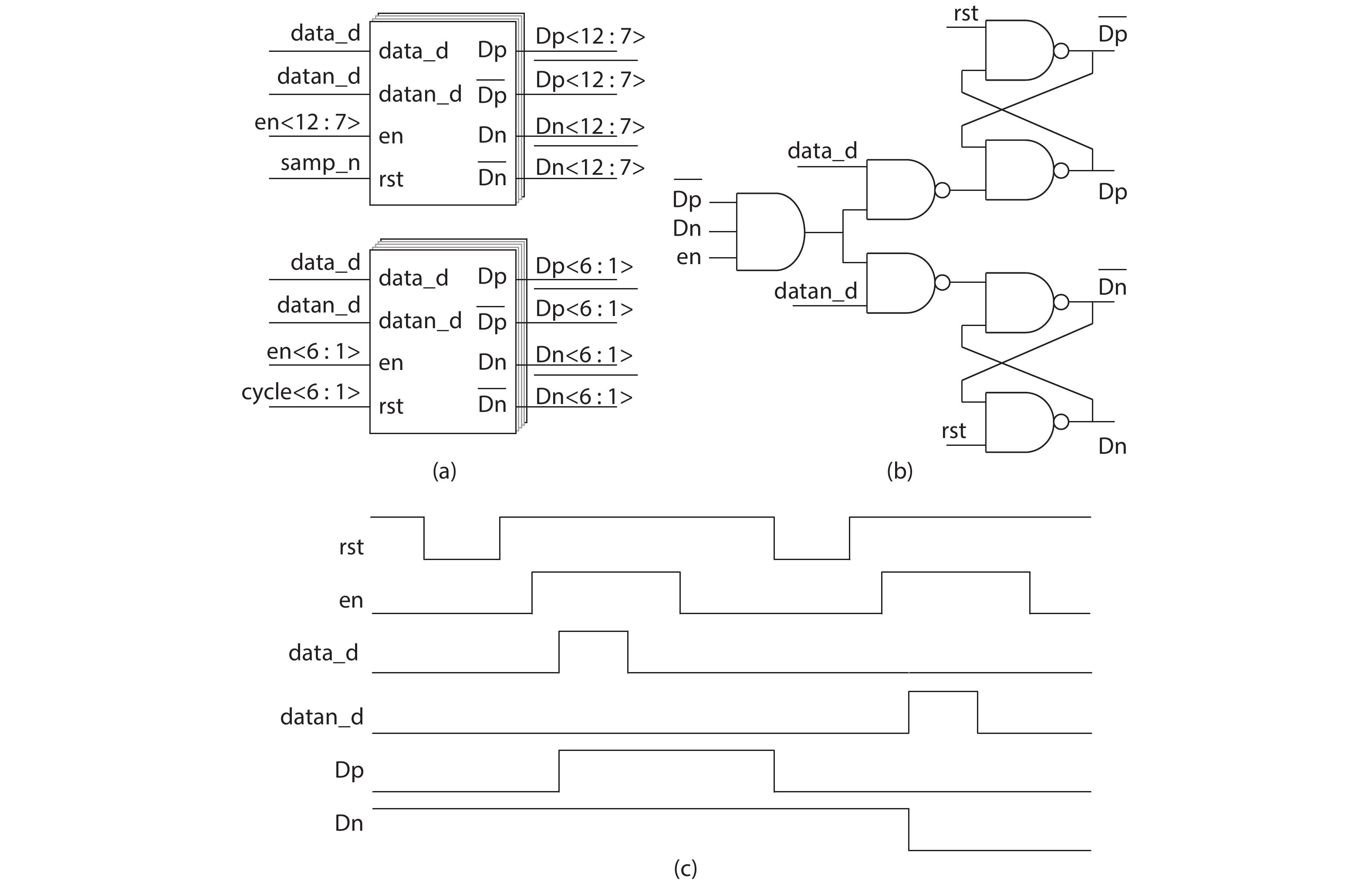
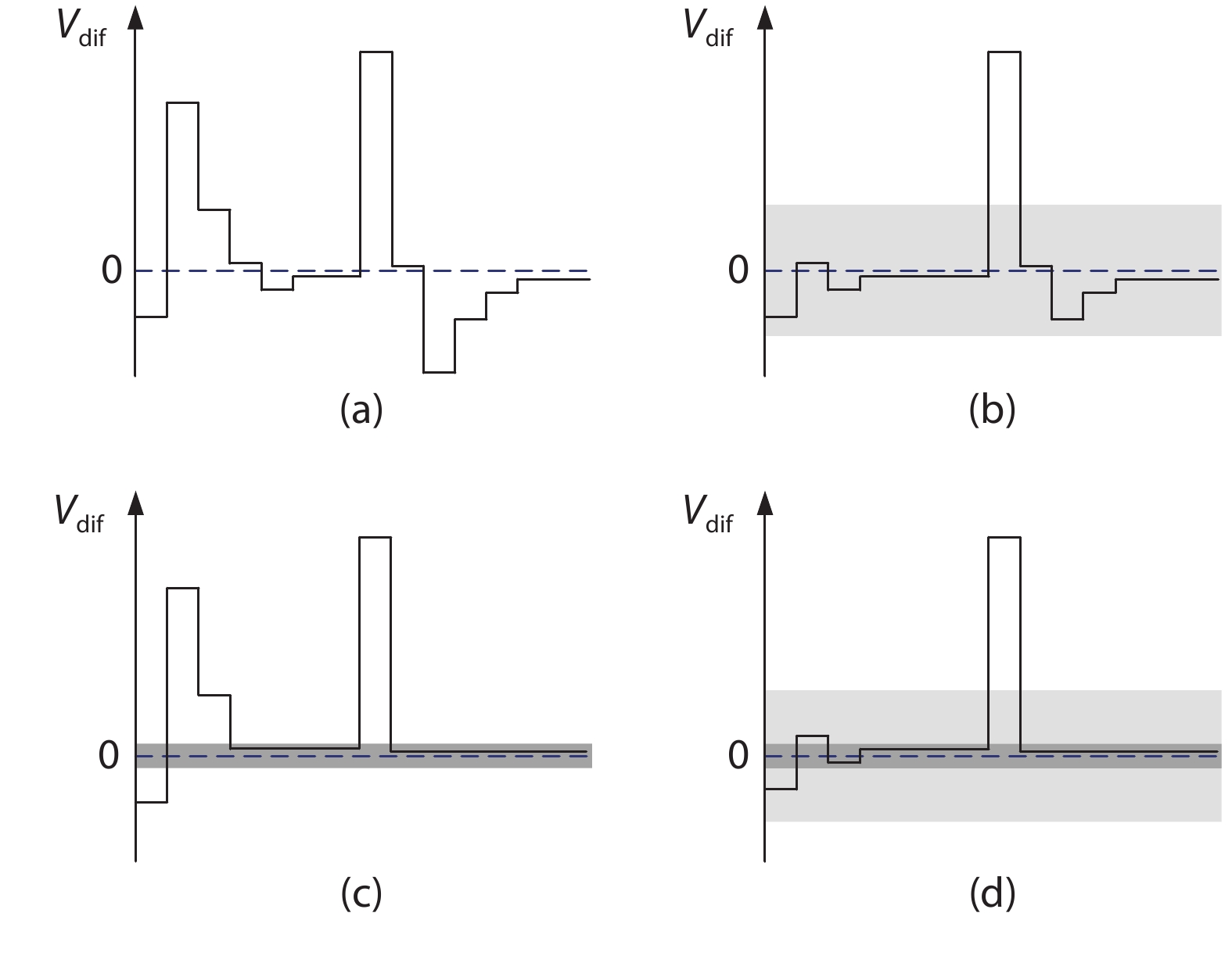
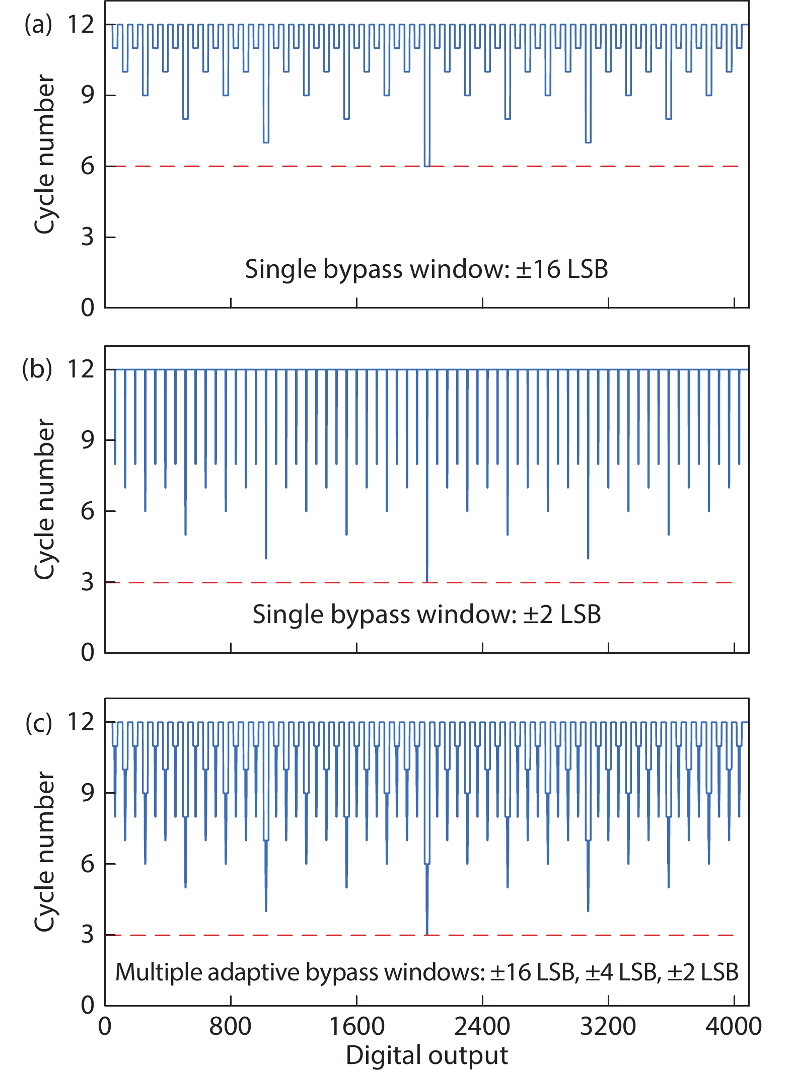
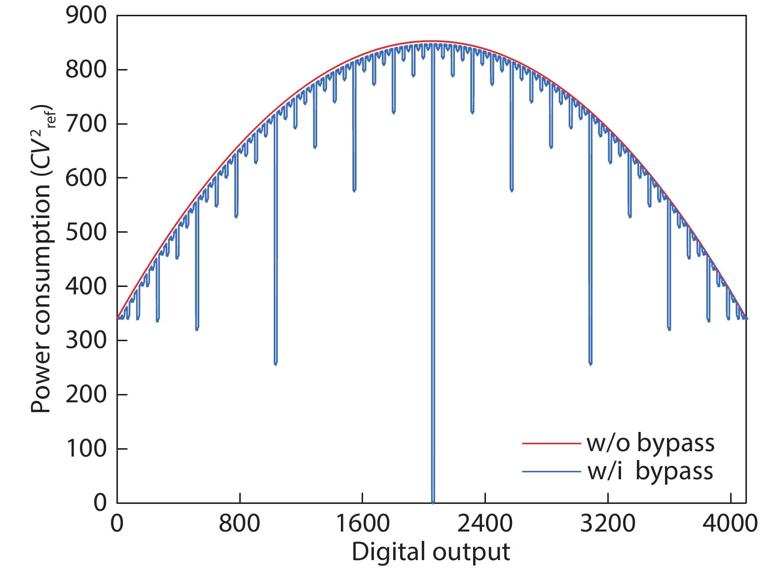
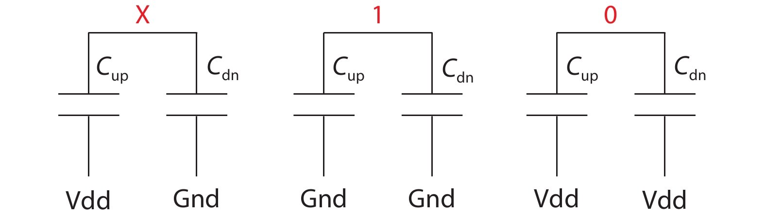
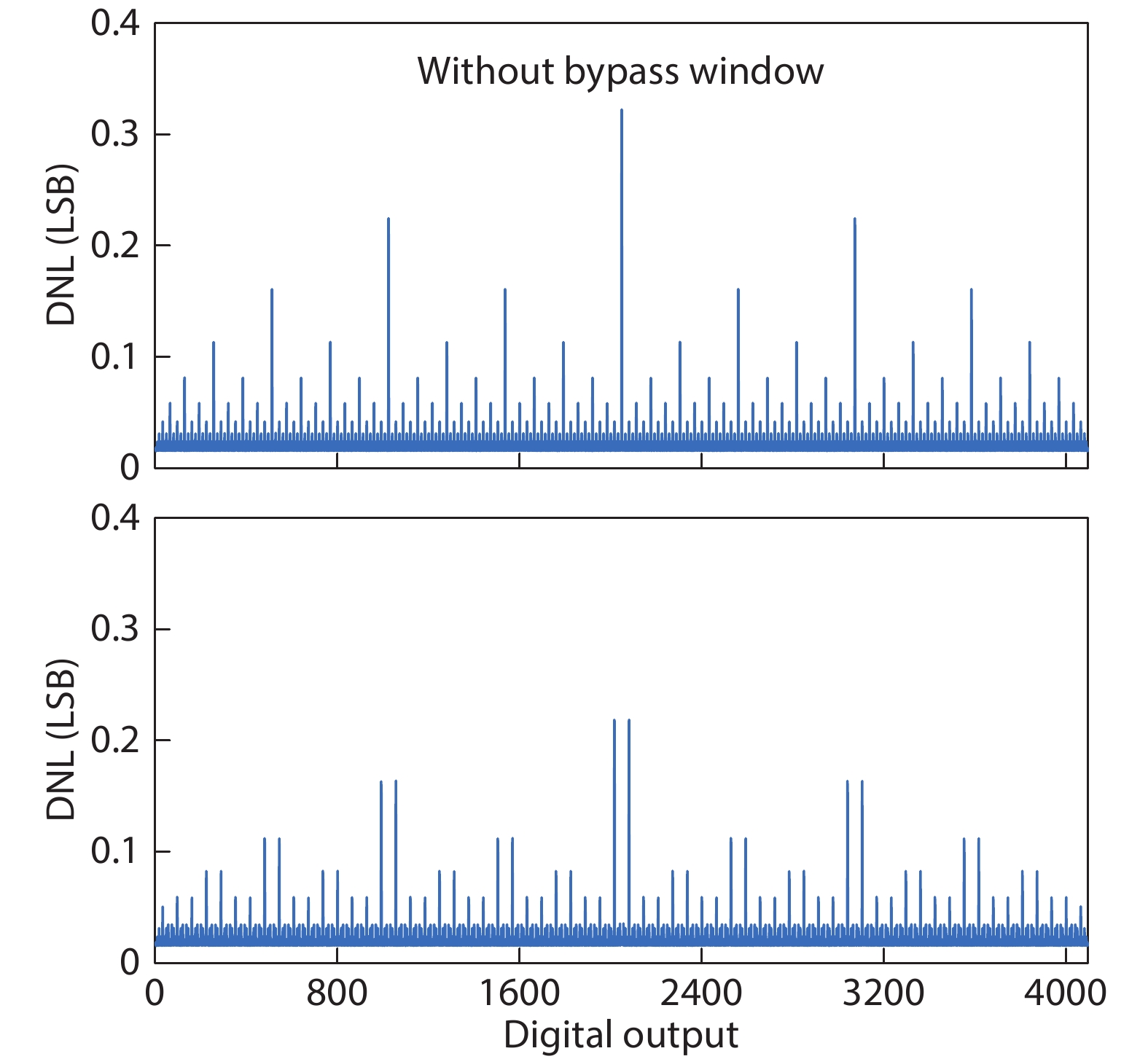
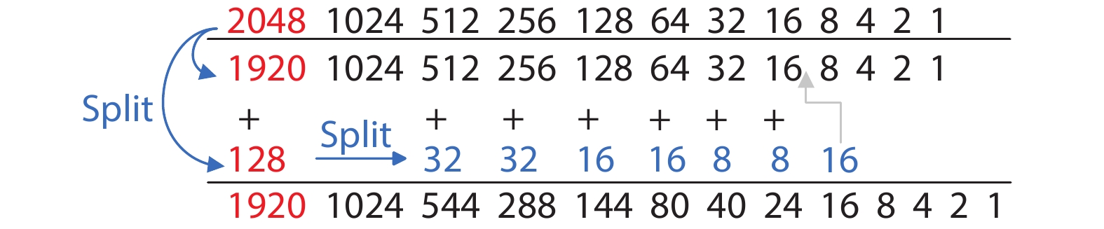
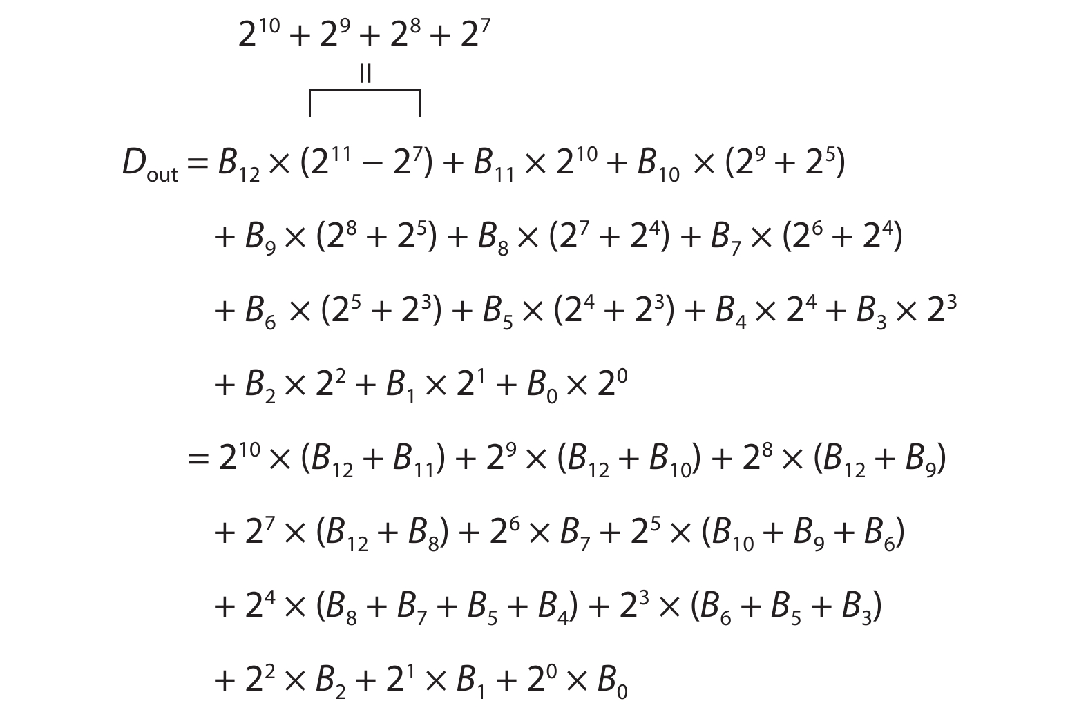
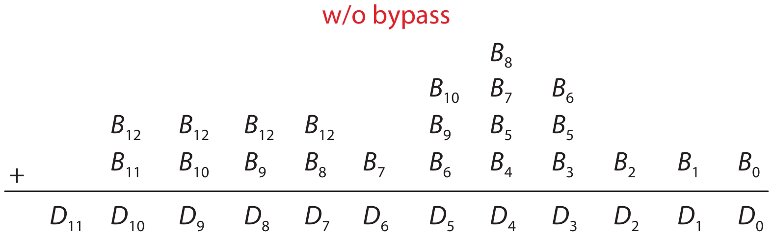
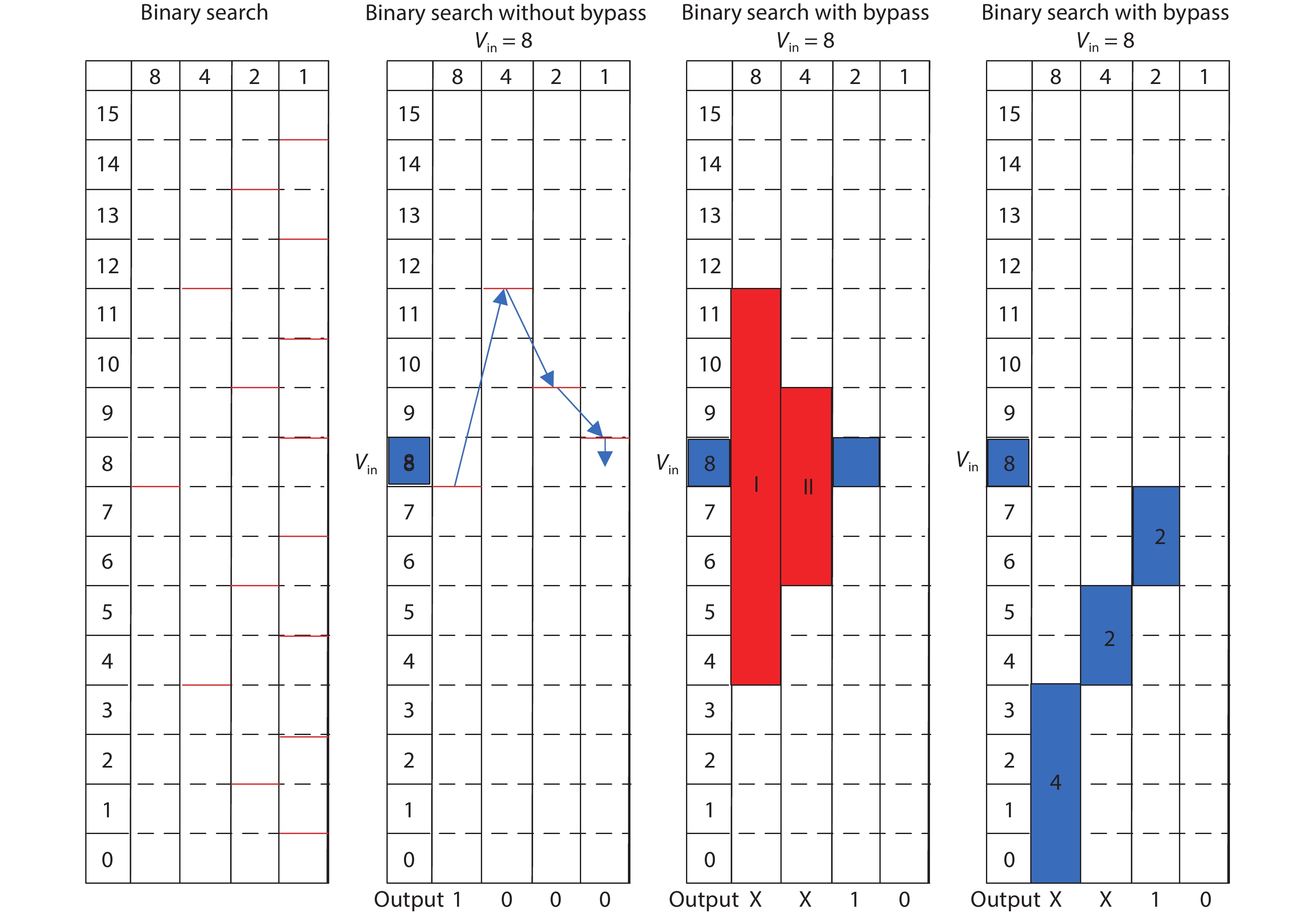
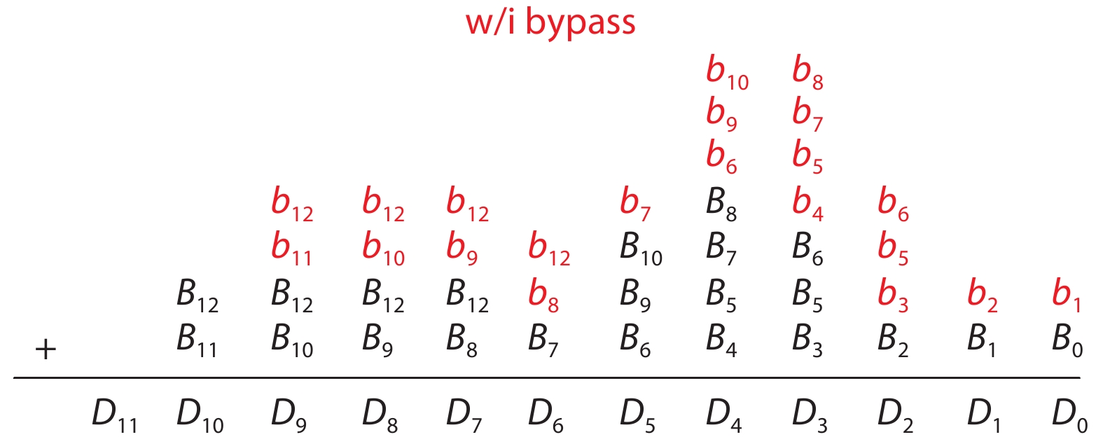
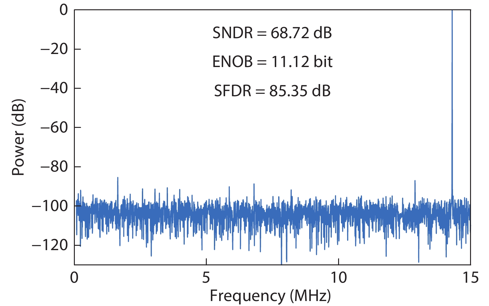
This paper proposes a technique that uses the number of oscillation cycles (NOC) of a VCO-based comparator to set multiple adaptive bypass windows in a 12-bit successive approximation register (SAR) analog-to-digital converter (ADC). The analysis of the number of bit cycles, power and static performance shows that three adaptive bypass windows reduce power consumption, and decrease DNL and have similar INL, compared with the SAR ADC without bypass windows. In addition, a 1-bit split-and-recombination redundancy technique and a general bypass logic digital error correction method are proposed to address the settling issues and optimize the size of the bypass window. This design is implemented in 40 nm CMOS technology. The conversion frequency of the ADC reaches up to 30 MS/s. The ADC achieves an SFDR of 85.35 dB and 11.12-bit ENOB with Nyquist input, consuming 380 μW, down from 427 μW without multiple adaptive bypass windows, at a 1.1 V supply, resulting in a figure of merit (FoM) of 5.69 fJ/conversion-step.


J. Semicond.
2020, 41(11): 112402 doi: 10.1088/1674-4926/41/11/112402
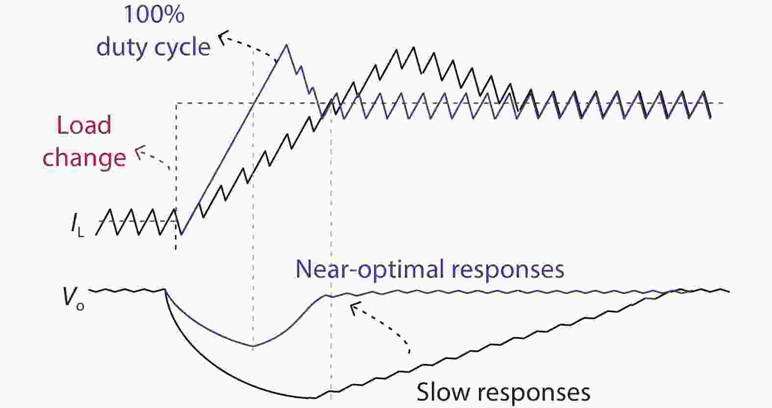
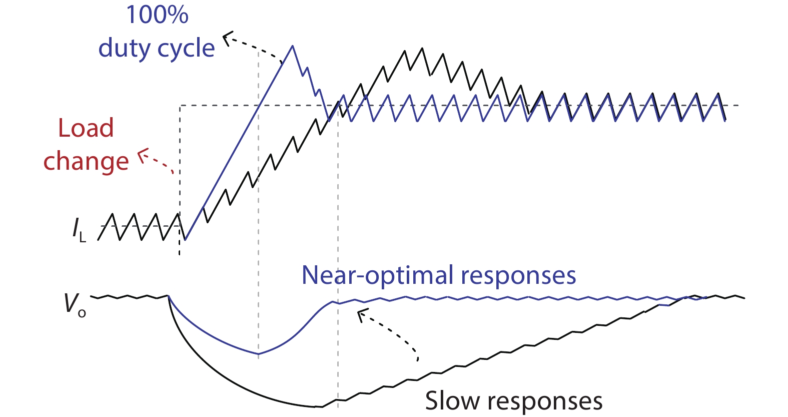
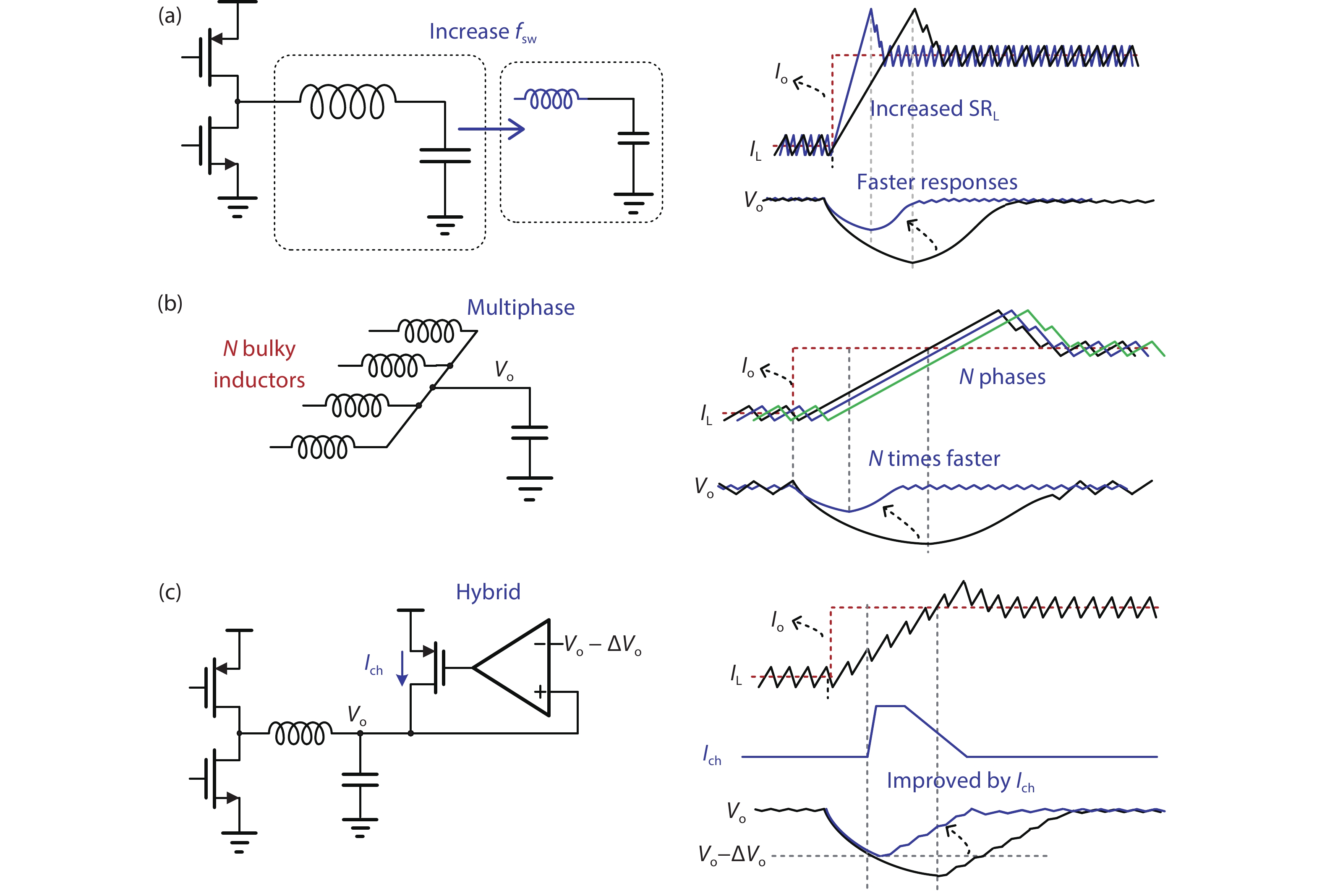
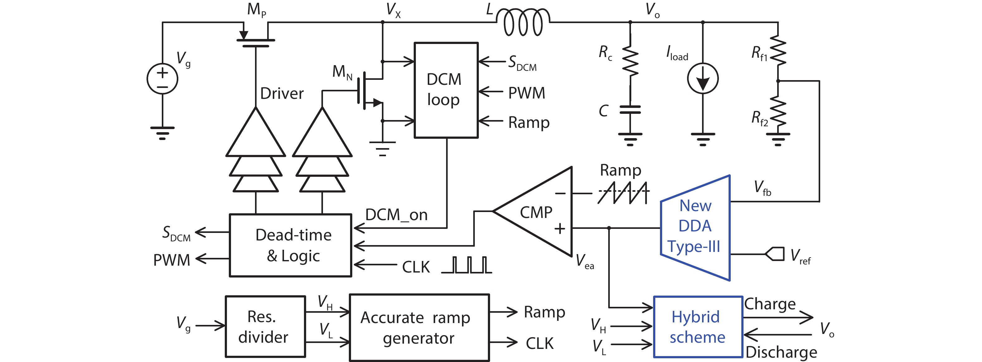
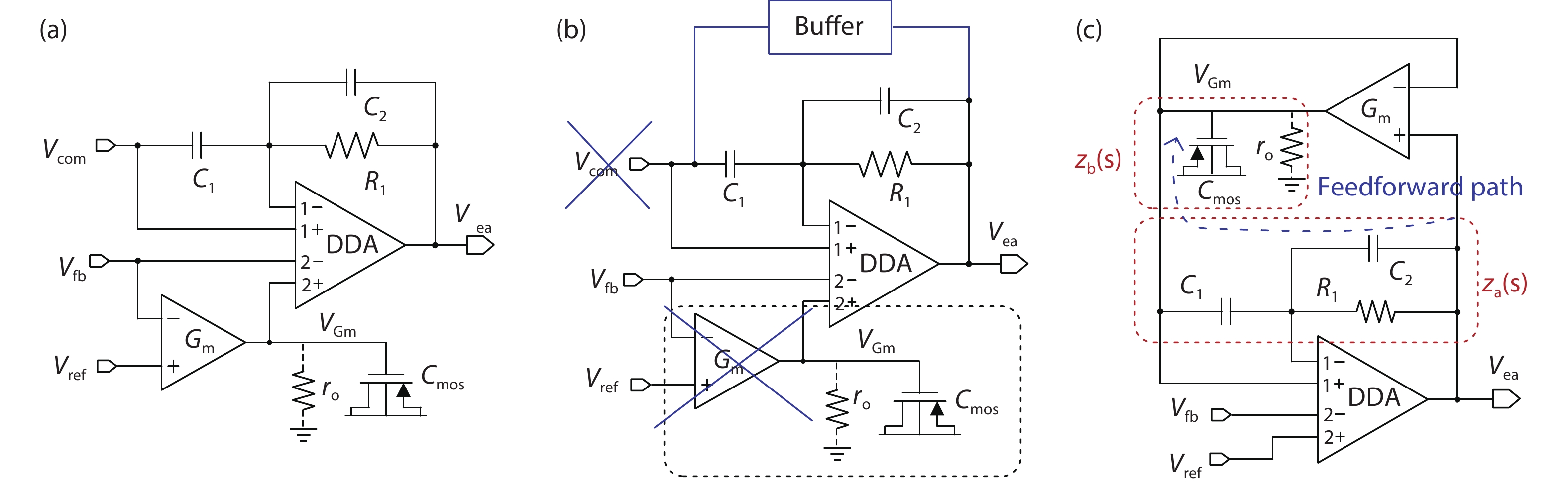
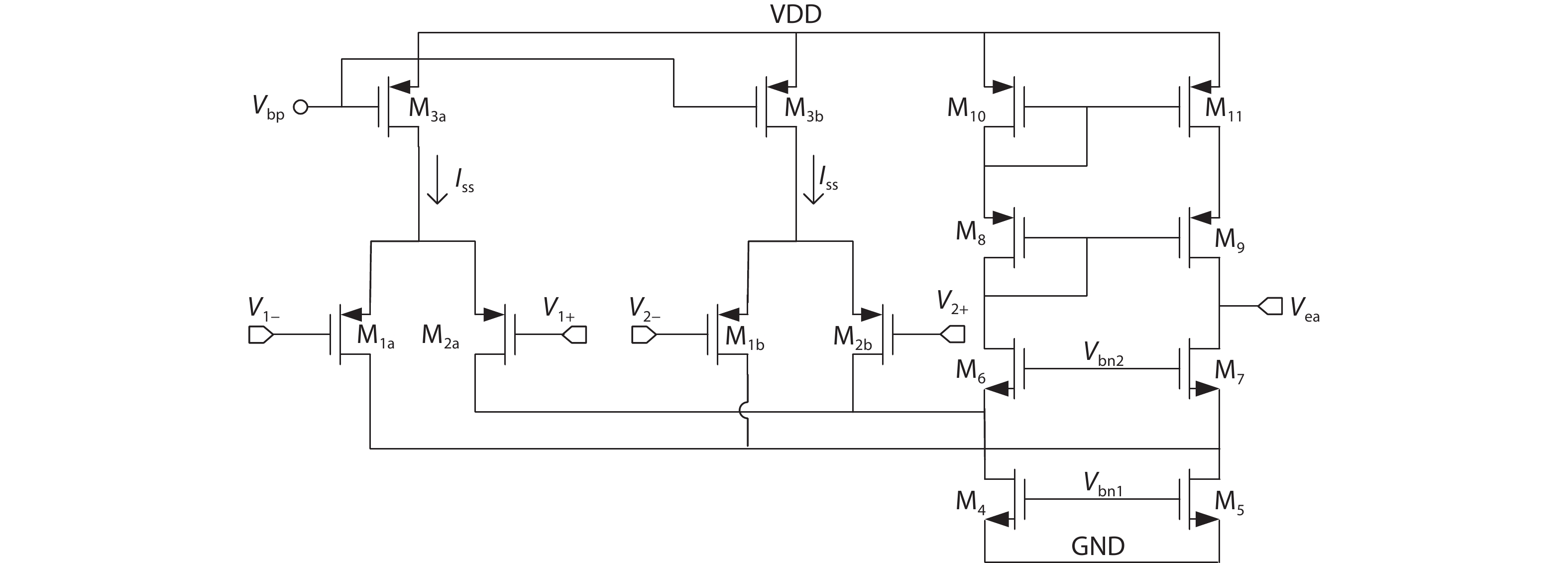
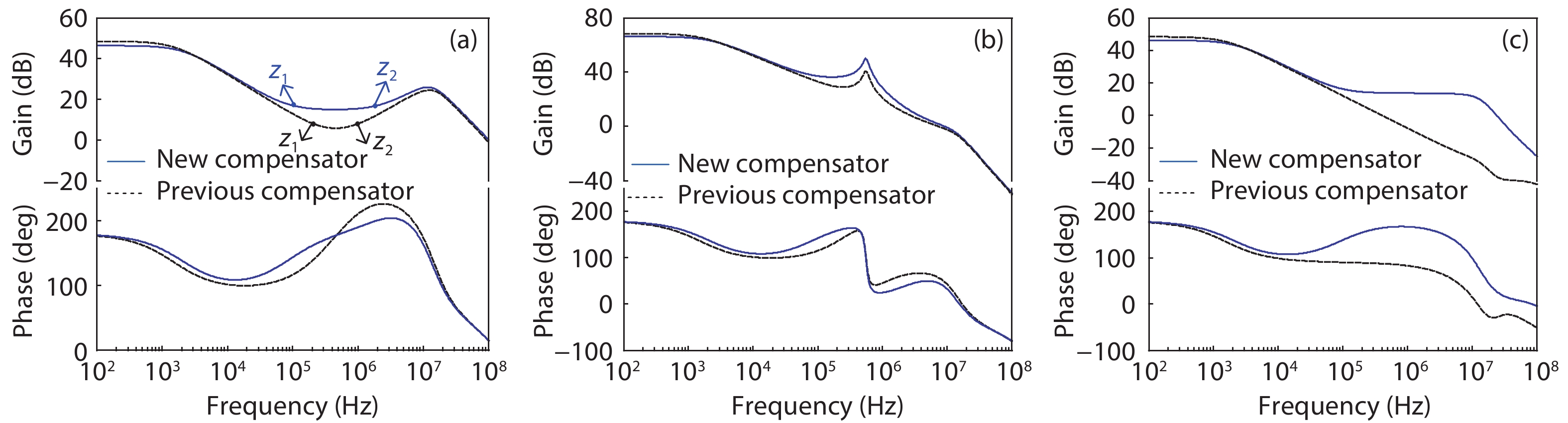
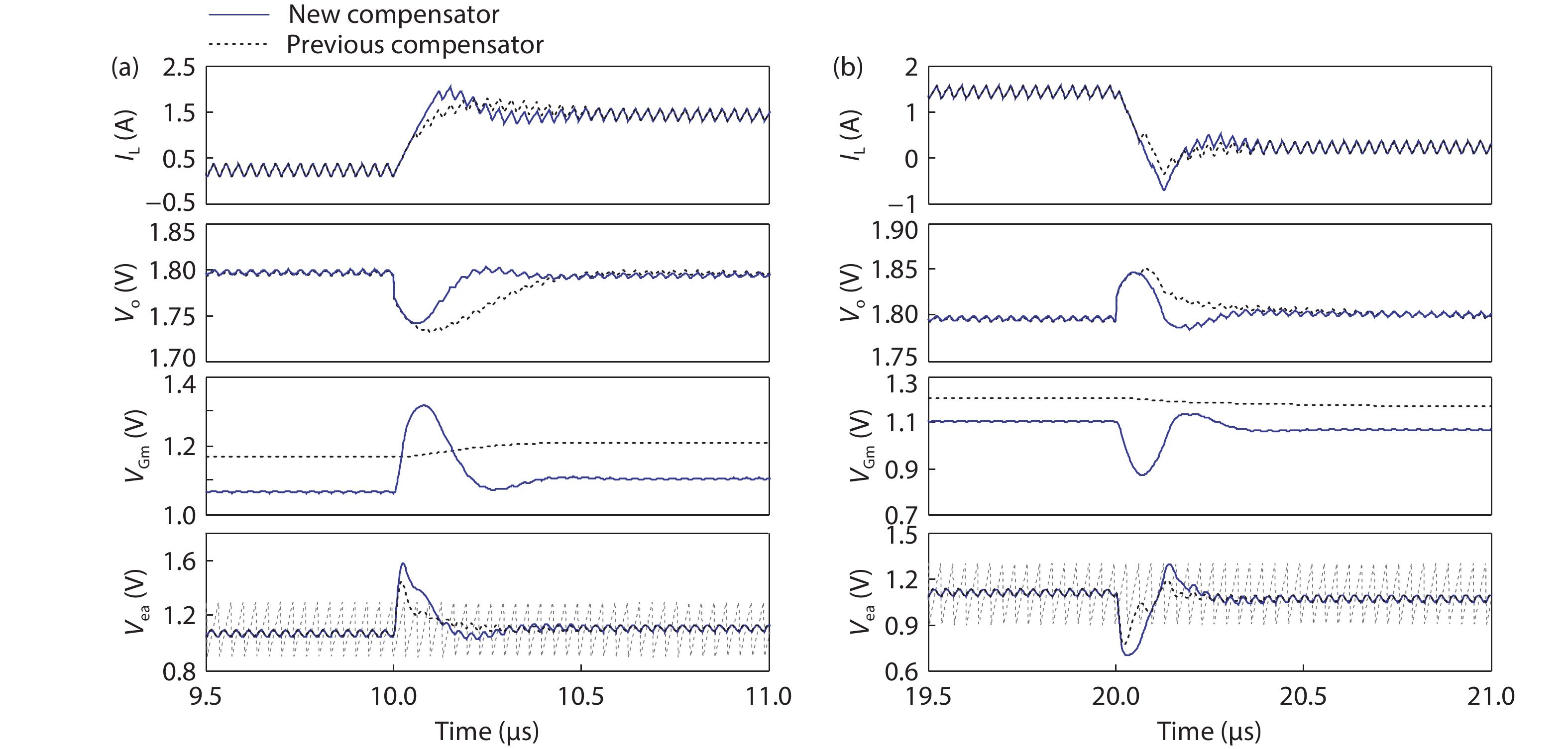
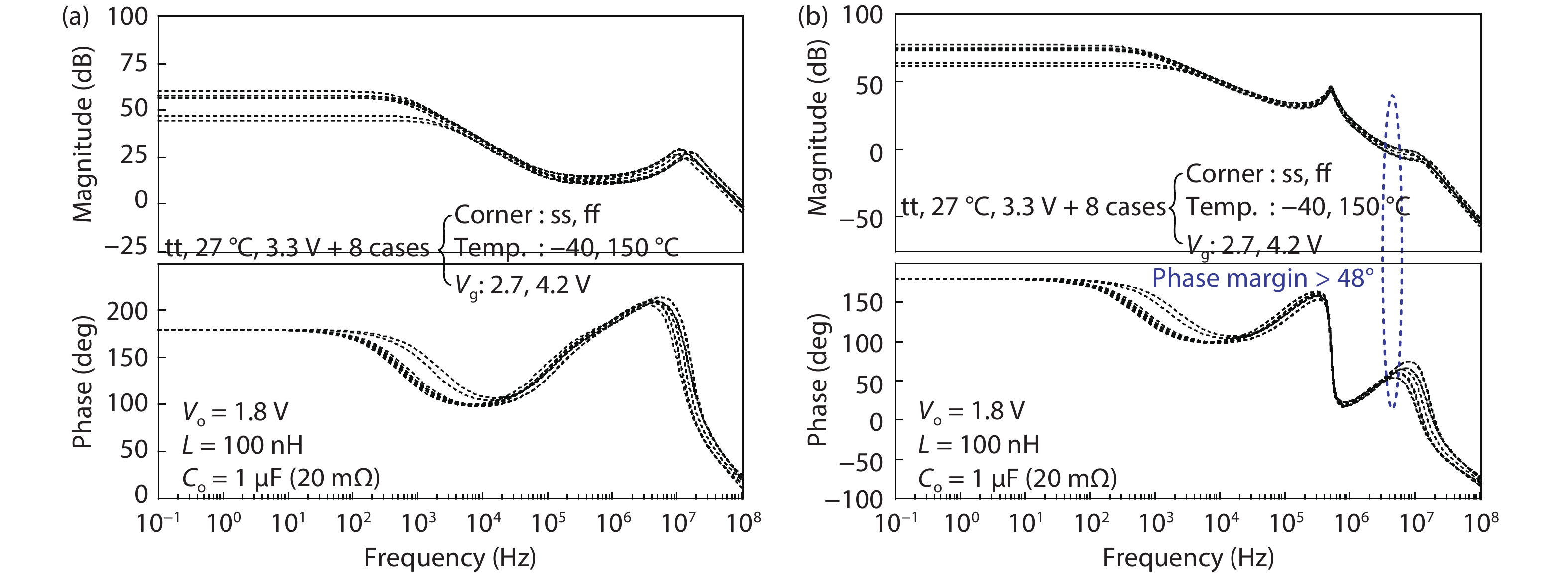
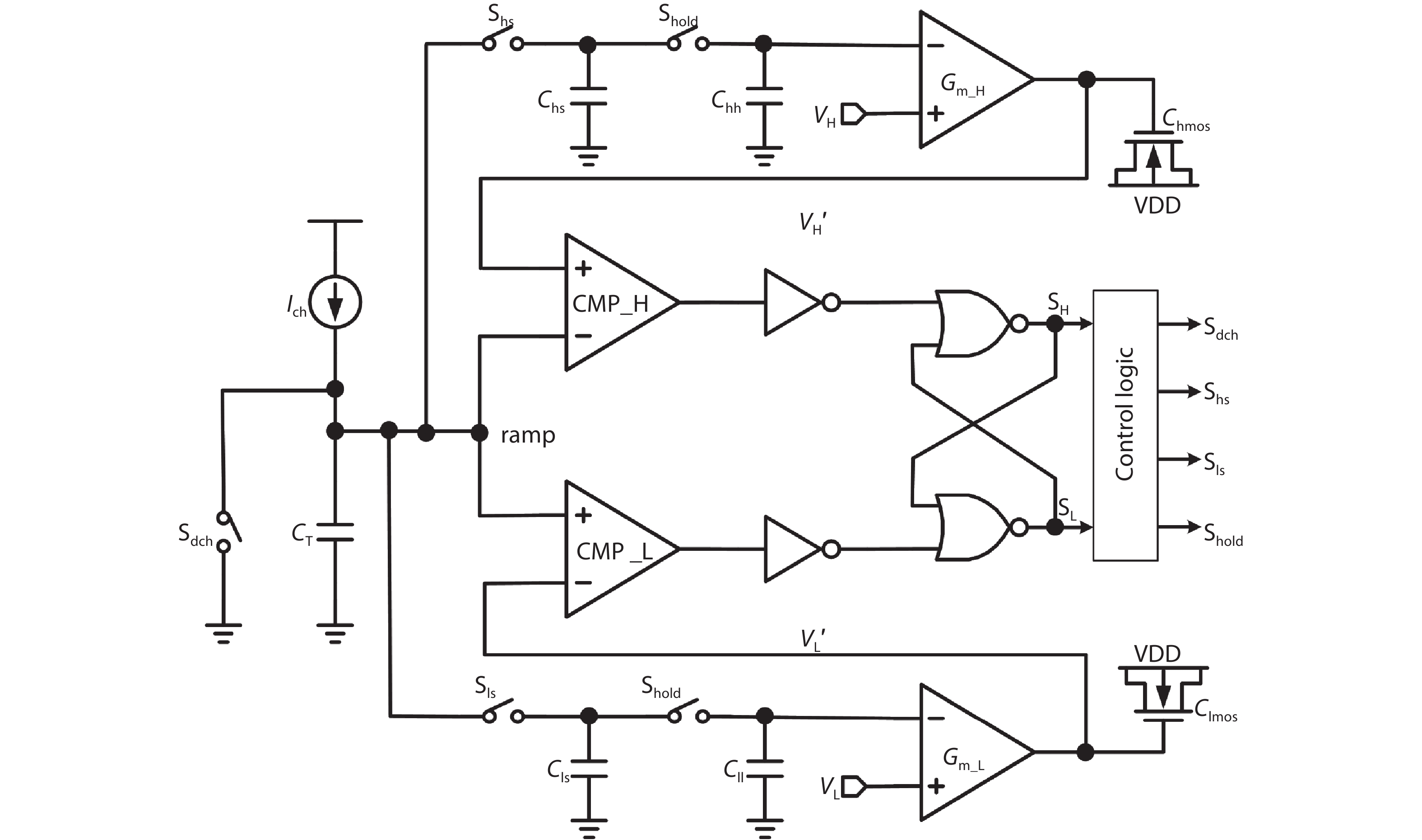
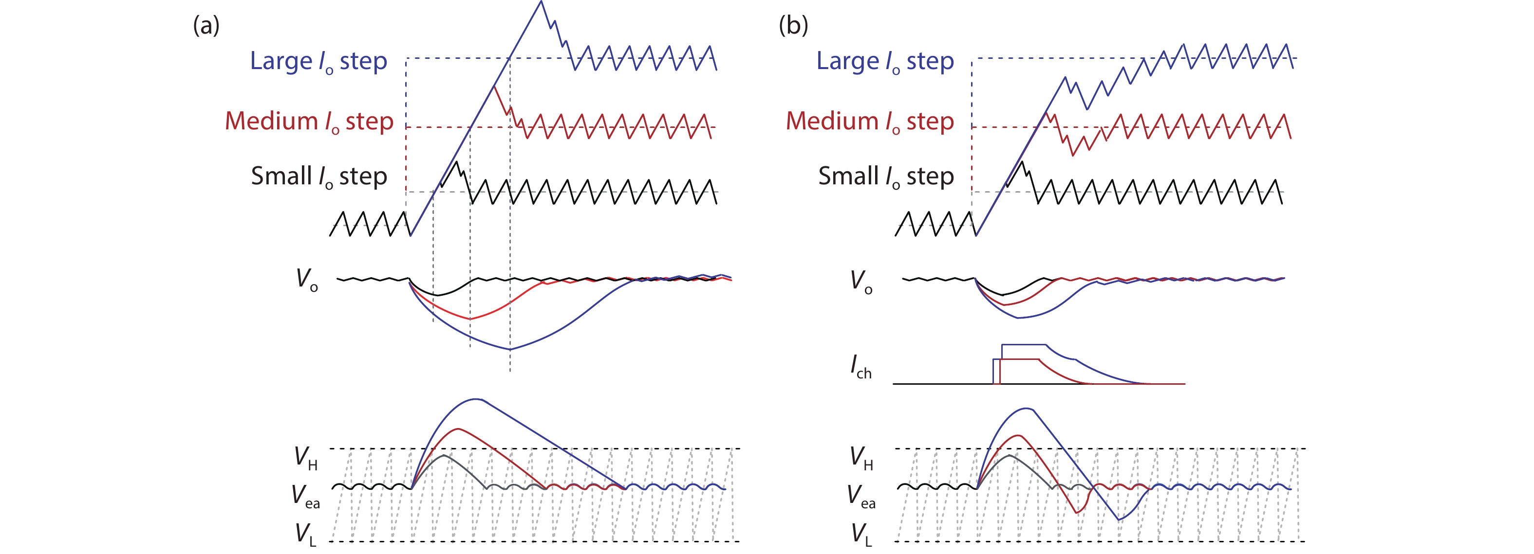
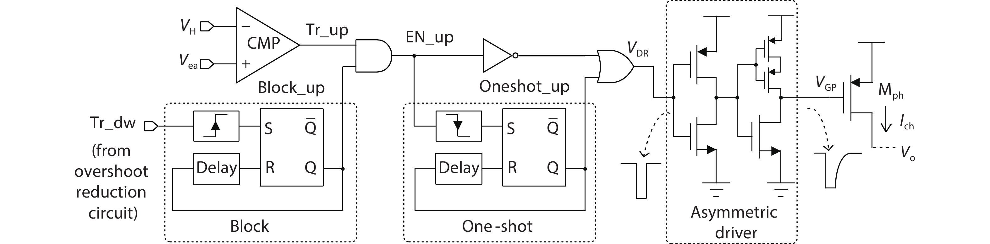
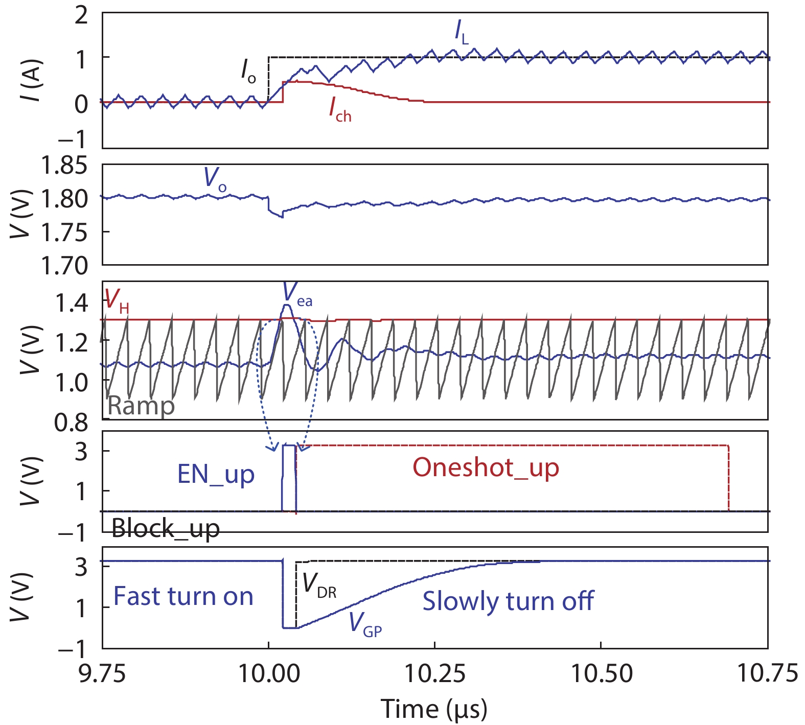
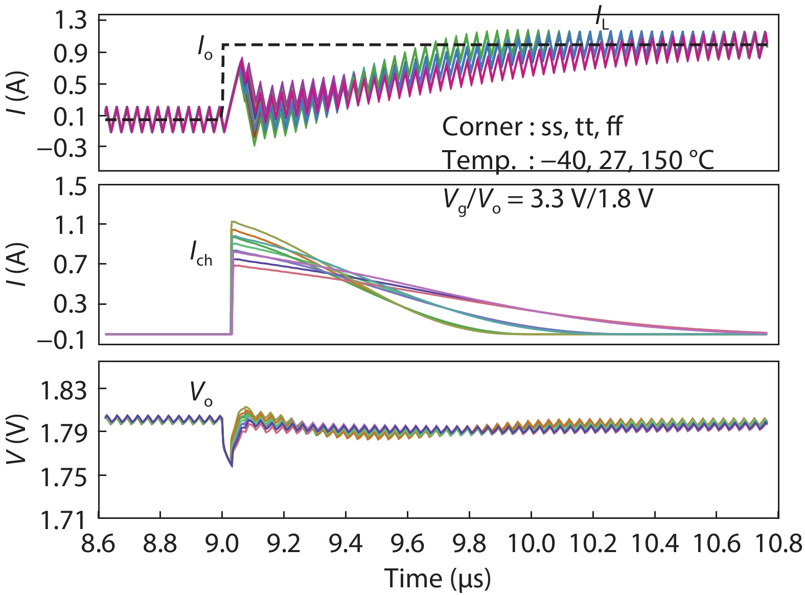
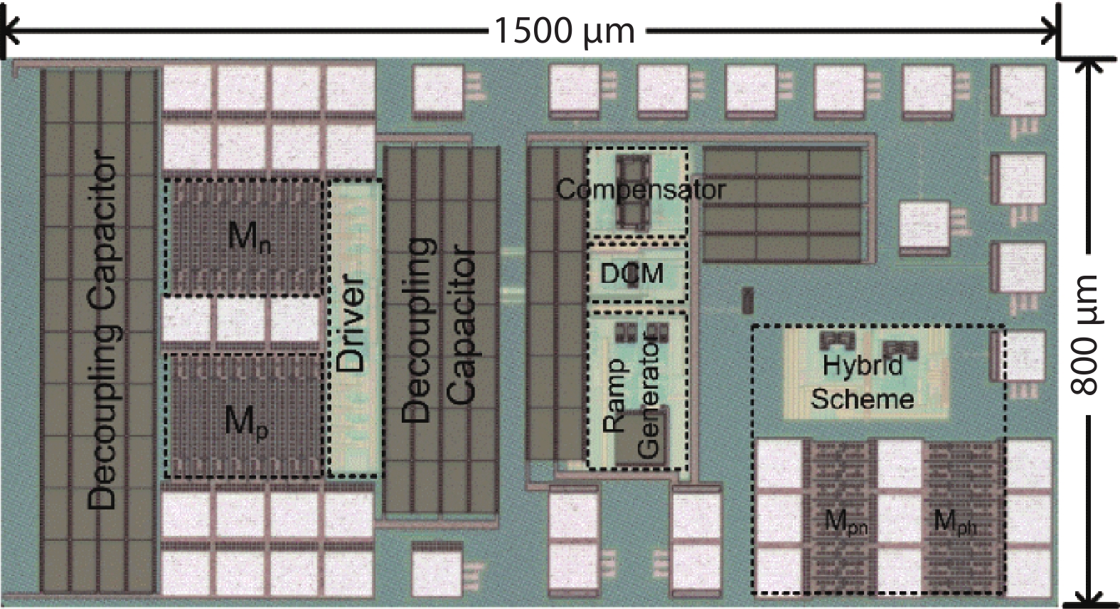
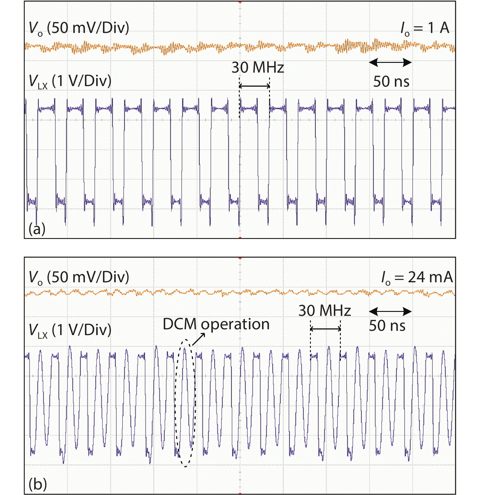
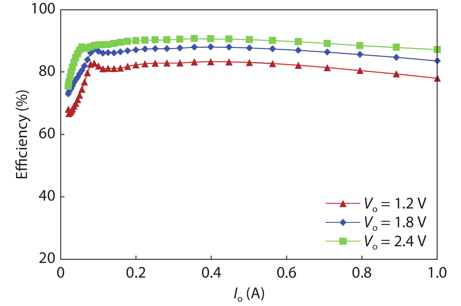
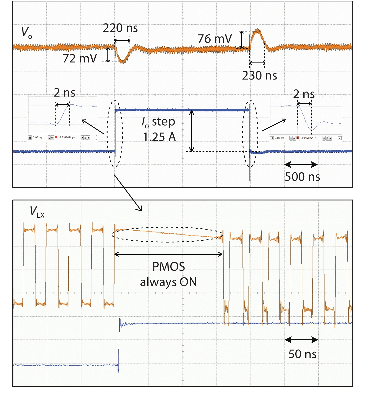
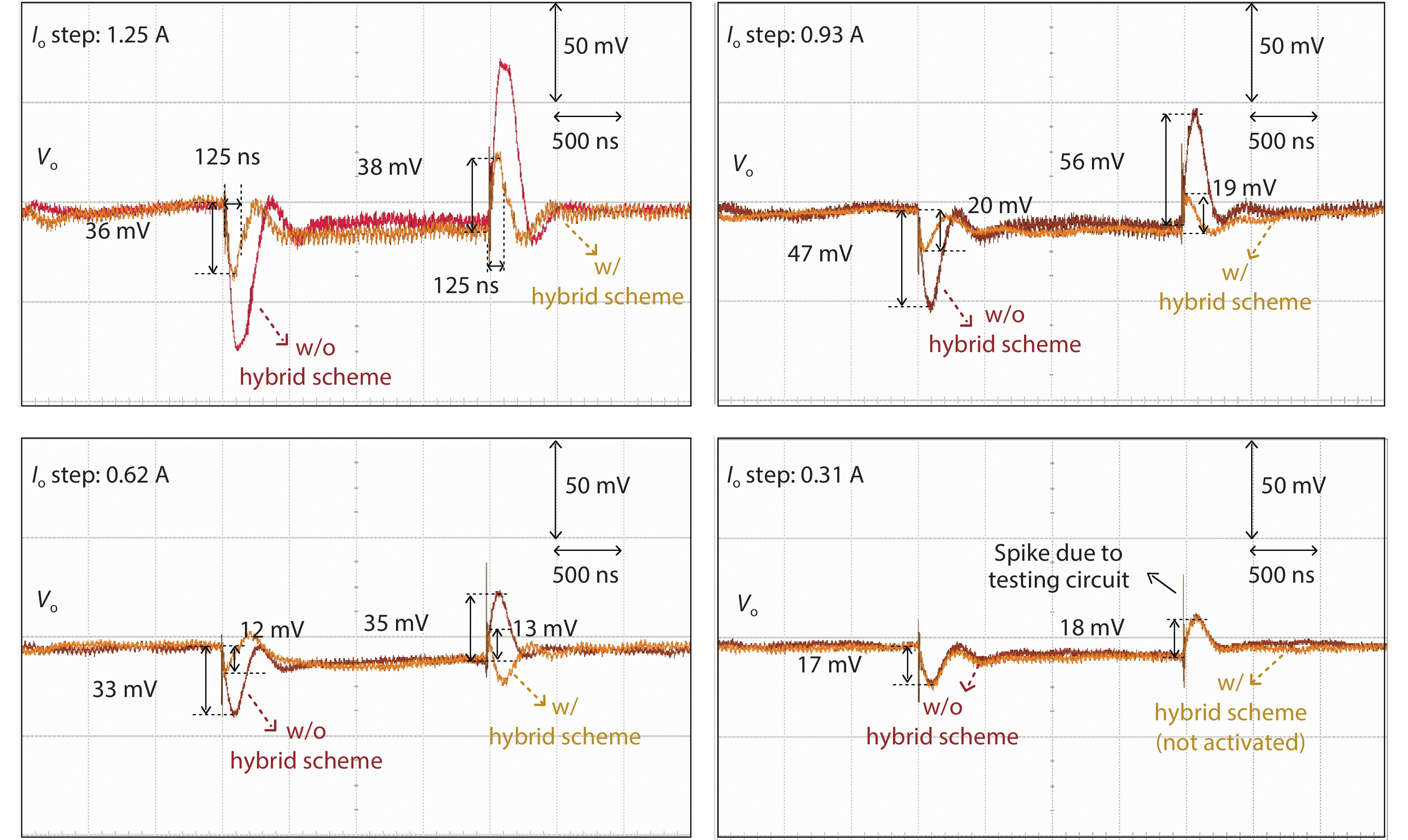
A 30 MHz voltage-mode controlled buck converter with fast transient responses is presented. An improved differential difference amplifier (DDA)-based Type-III compensator is proposed to reduce the settling times of the converter during load transients, and to achieve near-optimal transient responses with simple PWM control only. Moreover, a hybrid scheme using a digital linear regulator with automatic transient detection and seamless loop transition is proposed to further improve the transient responses. By monitoring the output voltage of the compensator instead of the output voltage of the converter, the proposed hybrid scheme can reduce undershoot and overshoot effectively with good noise immunity and without interrupting the PWM loop. The converter was fabricated in a 0.13 µm standard CMOS process using 3.3 V devices. With an input voltage of 3.3 V, the measured peak efficiencies at the output voltages of 2.4, 1.8, and 1.2 V are 90.7%, 88%, and 83.6%, respectively. With a load step of 1.25 A and rise and fall times of 2 ns, the measured 1% settling times were 220 and 230 ns, with undershoot and overshoot with PWM control of 72 and 76 mV, respectively. They were further reduced to 36 and 38 mV by using the proposed hybrid scheme, and 1% settling times were also reduced to 125 ns.