Surface acoustic wave (SAW) devices have been widely used in different fields and will continue to be of great importance in the foreseeable future. These devices are compact, cost efficient, easy to fabricate, and have a high performance, among other advantages. SAW devices can work as filters, signal processing units, sensors and actuators. They can even work without batteries and operate under harsh environments. In this review, the operating principles of SAW sensors, including temperature sensors, pressure sensors, humidity sensors and biosensors, will be discussed. Several examples and related issues will be presented. Technological trends and future developments will also be discussed.
Issue Browser
Volume 37, Issue 2,
Feb 2016


J. Semicond.
2016, 37(2): 022001 doi: 10.1088/1674-4926/37/2/022001
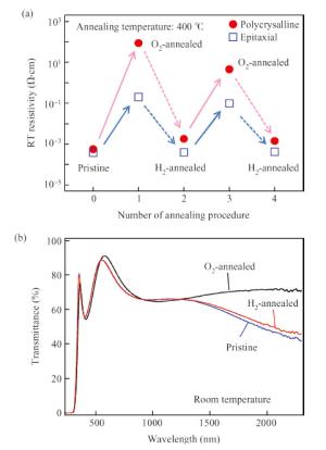
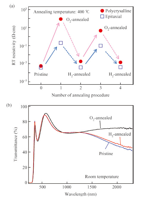
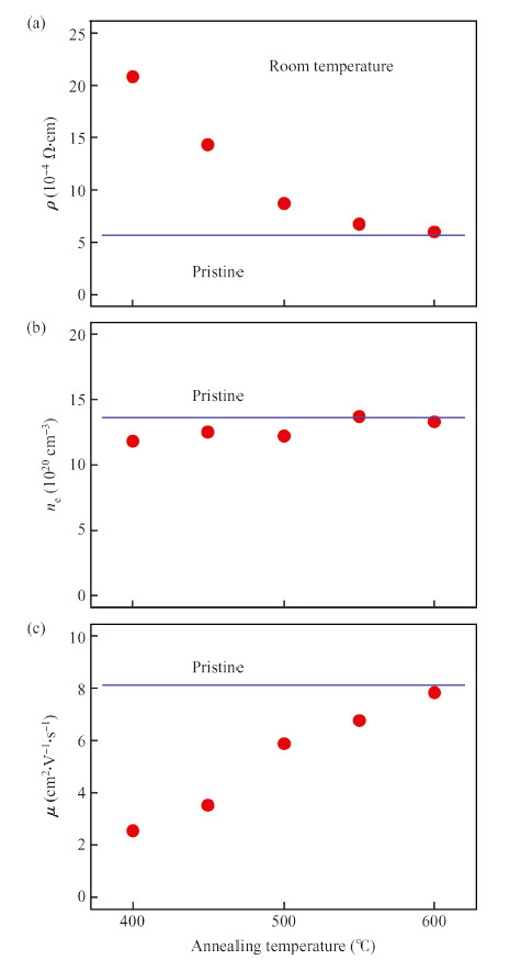
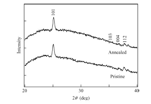
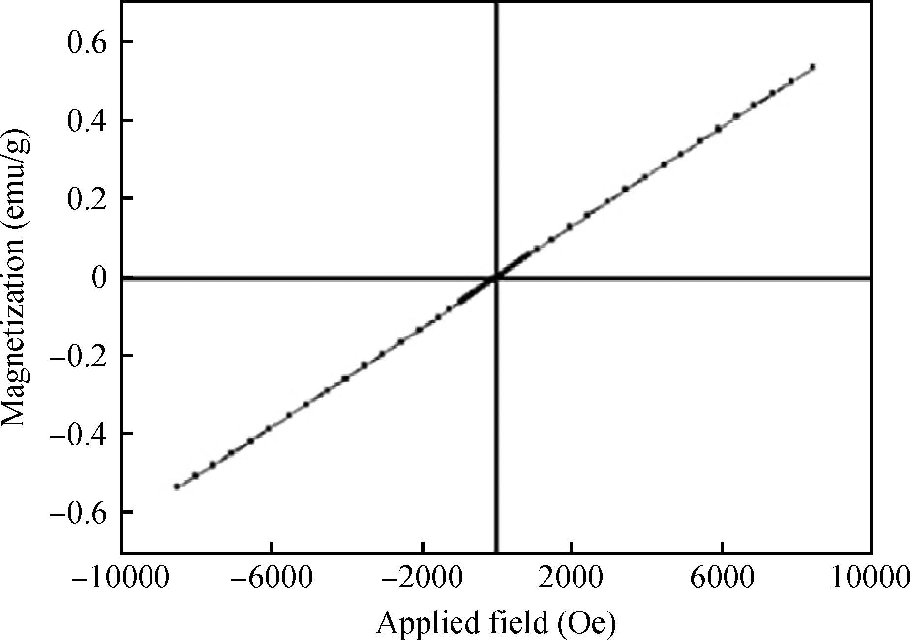
We studied the effects of reductive annealing on insulating polycrystalline thin films of anatase Nb-doped TiO2 (TNO). The insulating TNO films were intentionally fabricated by annealing conductive TNO films in oxygen ambient at 400 ℃. Reduced free carrier absorption in the insulating TNO films indicated carrier compensation due to excess oxygen. With H2-annealing, both carrier density and Hall mobility recovered to the level of conducting TNO, demonstrating that the excess oxygen can be efficiently removed by the annealing process without introducing additional scattering centers.
J. Semicond.
2016, 37(2): 022002 doi: 10.1088/1674-4926/37/2/022002
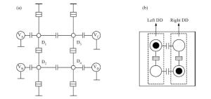
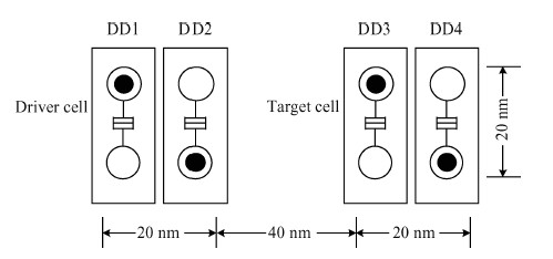
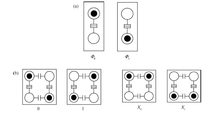
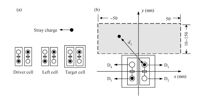
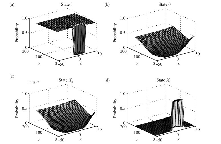
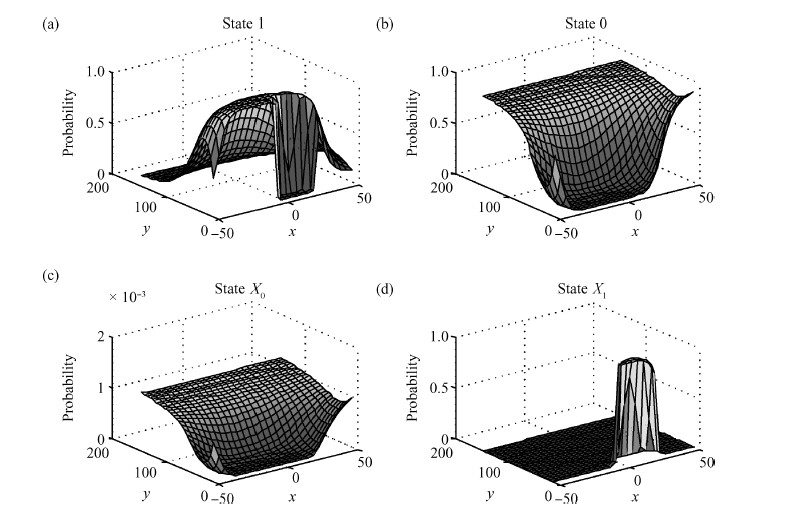
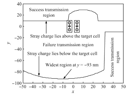
The behavior of quantum cellular automata (QCA) under the influence of a stray charge is quantified. A new time-independent switching paradigm, a probability model of the double-dot system, is developed. Superiority in releasing the calculation operation is presented by the probability model compared to previous stray charge analysis utilizing ICHA or full-basis calculation. Simulation results illustrate that there is a 186-nm-wide region surrounding a QCA wire where a stray charge will cause the target cell to switch unsuccessfully. The failure is exhibited by two new states' dominating the target cell. Therefore, a bistable saturation model is no longer applicable for stray charge analysis.

J. Semicond.
2016, 37(2): 023001 doi: 10.1088/1674-4926/37/2/023001

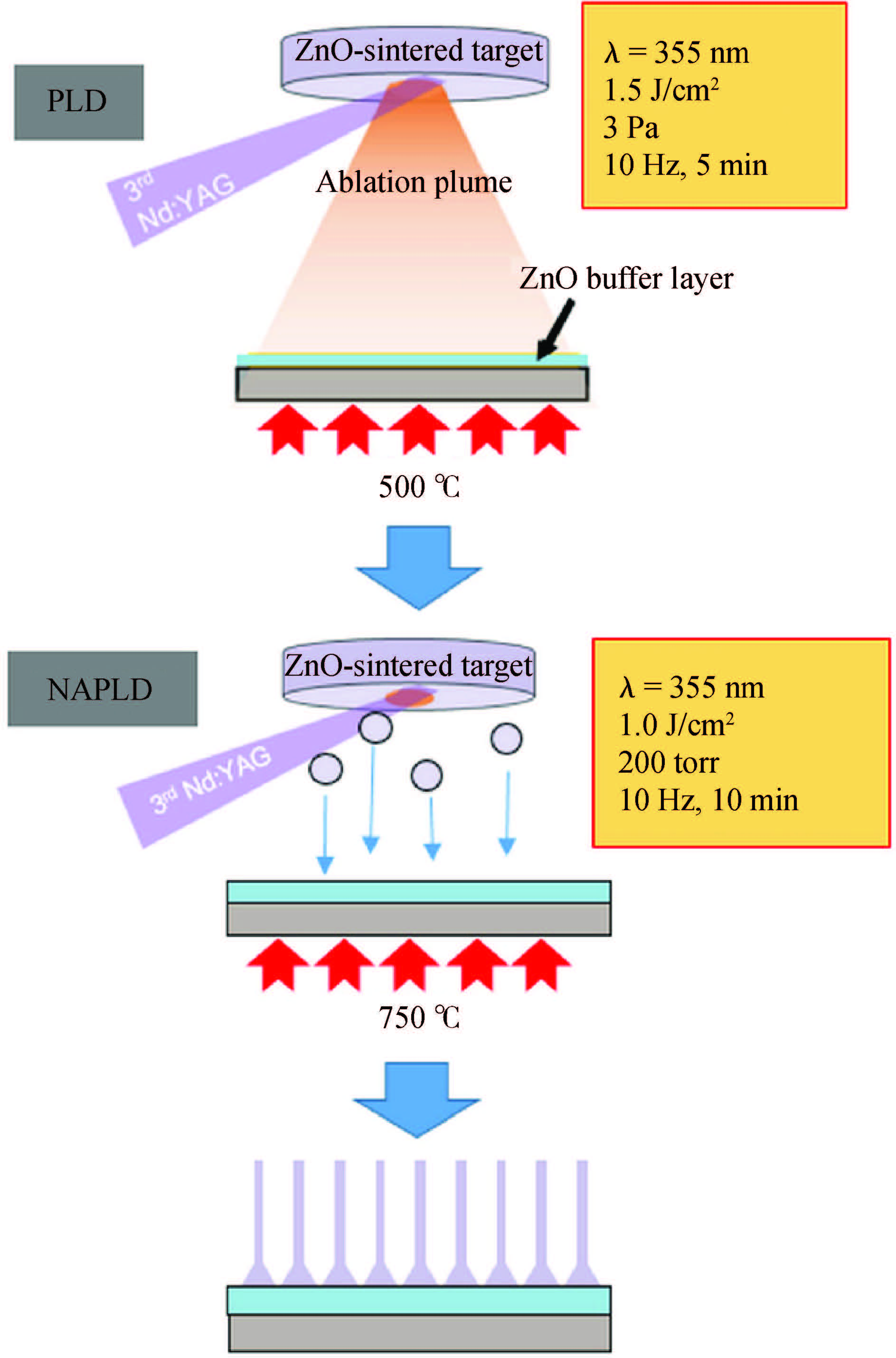
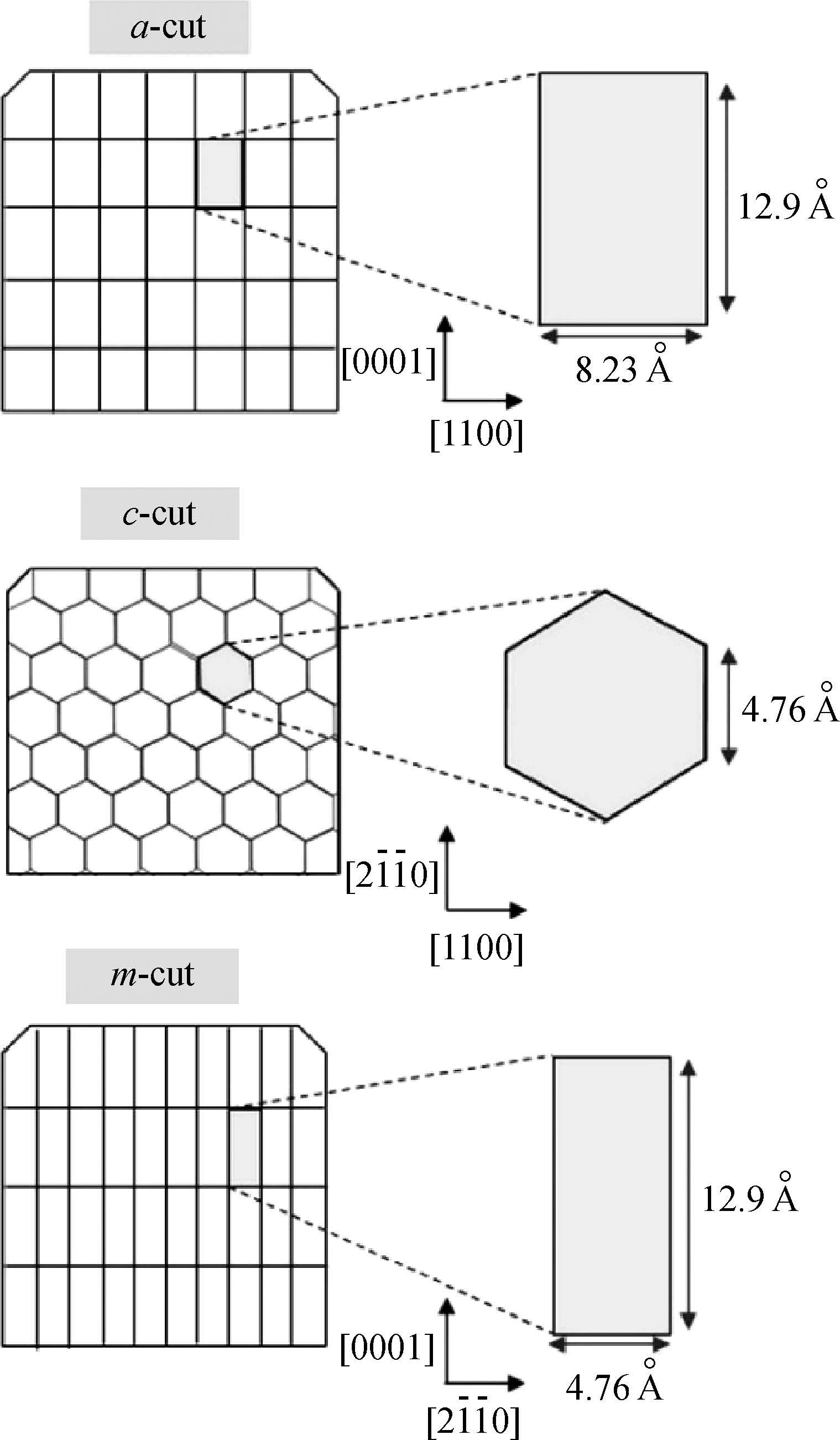
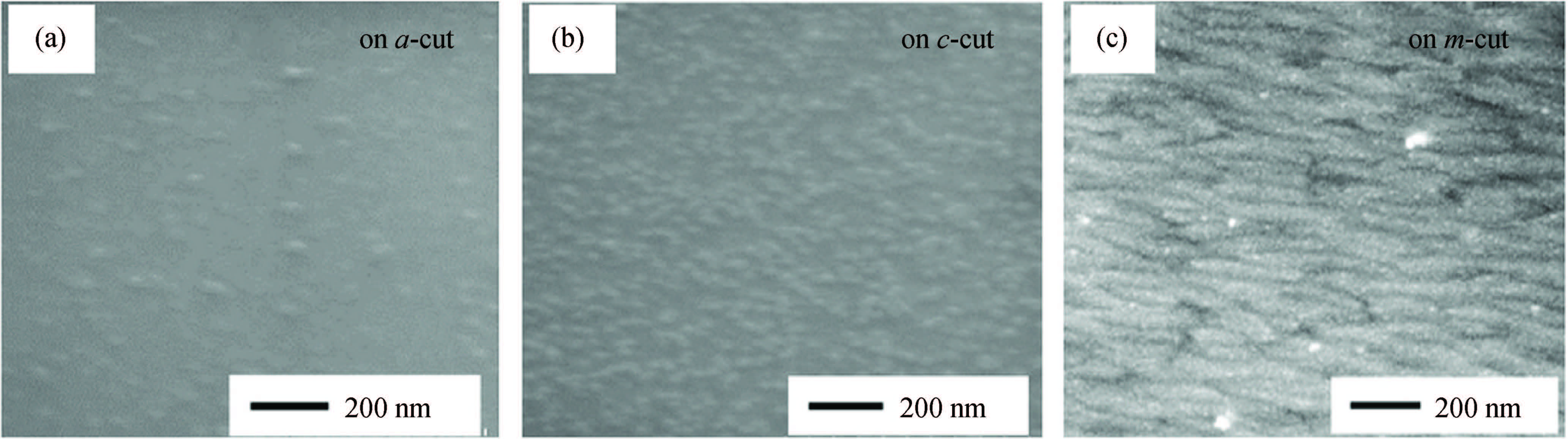
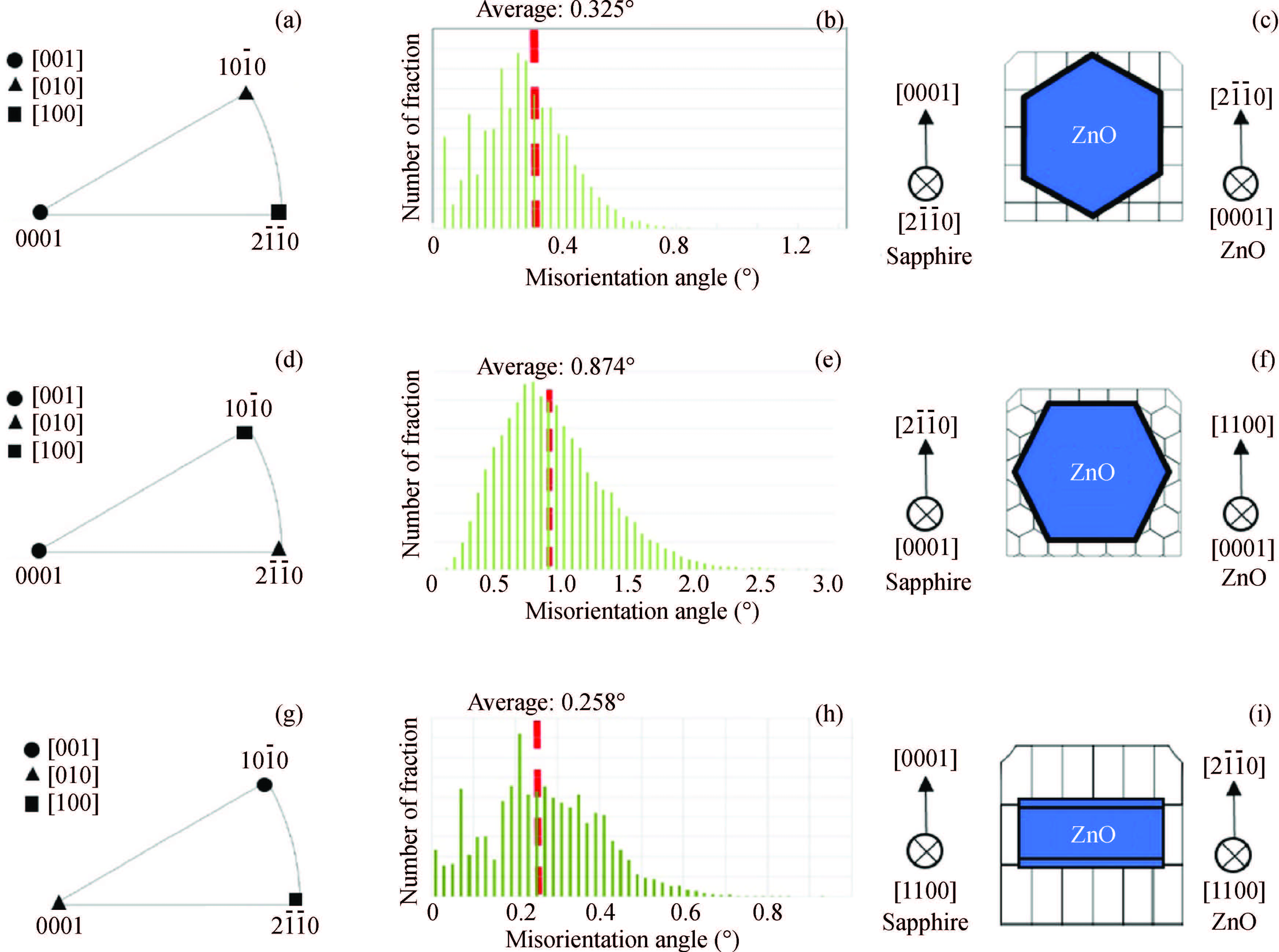
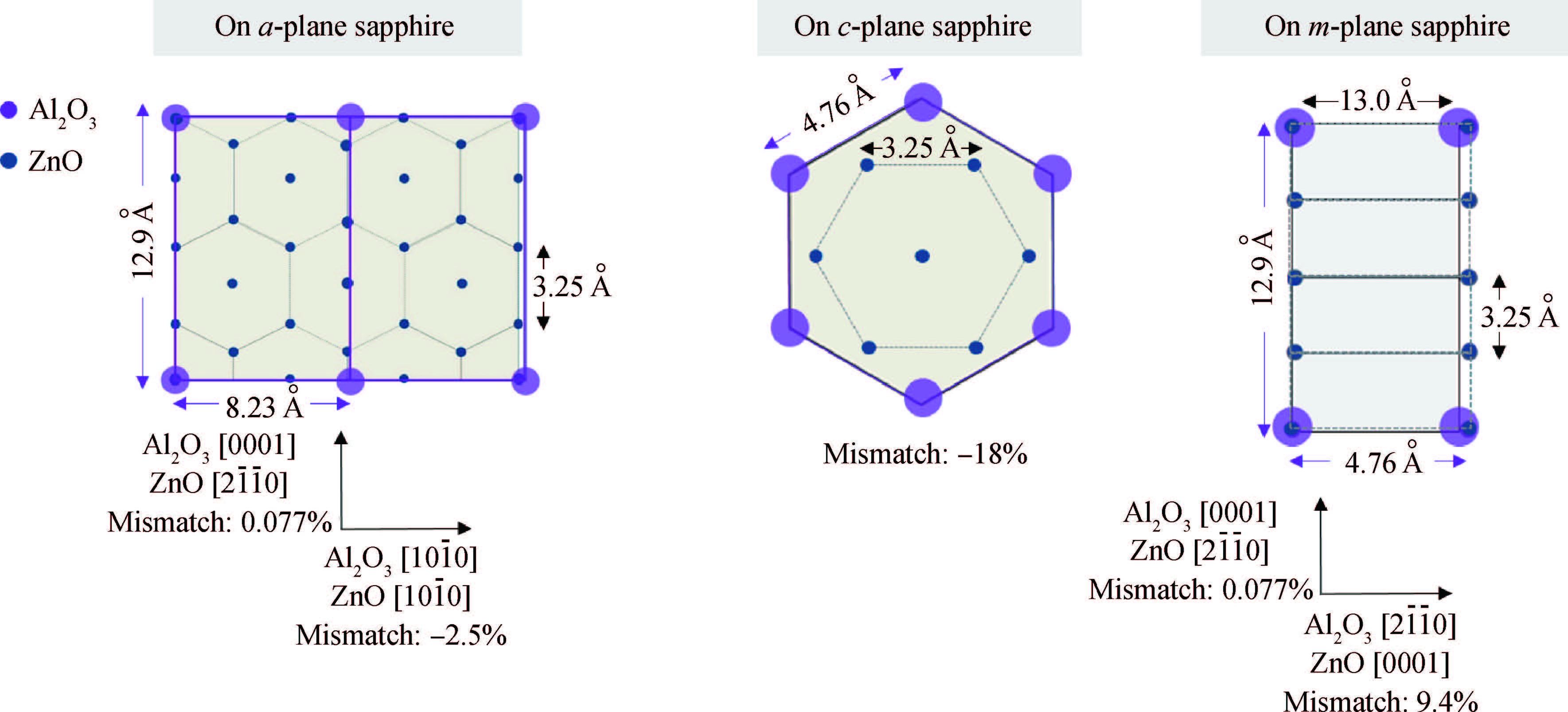
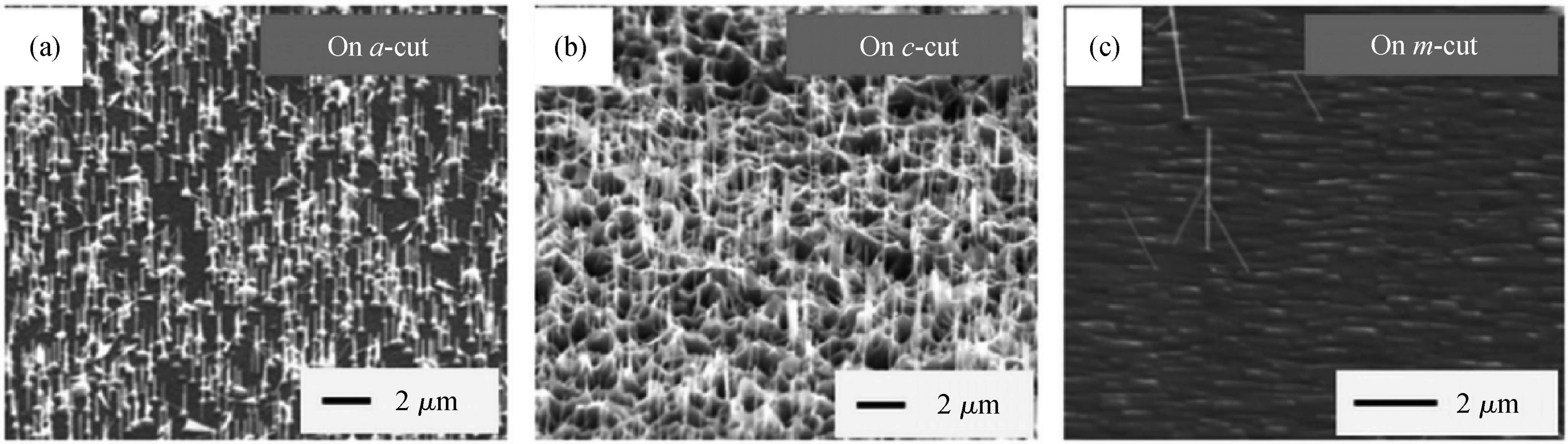
Catalyst-free growth of one-dimensional zinc oxide (ZnO) nanowires is reported. ZnO nanowires were synthesized on ZnO buffer layers deposited on various-oriented sapphire substrates. Syntheses of ZnO buffer layers and nanowires were performed by ultraviolet pulsed-laser deposition. ZnO nanowire's number density was the lowest in the case of using m-cut sapphire substrates. ZnO nanowires grown on a-cut sapphire substrates had vertical alignment with distances of tens to hundreds of nanometers. On the other hand, ZnO nanowires grown on c-cut sapphire substrates had the biggest nucleation rate. The dependence of crystalline orientation of ZnO buffer layers on the orientation of sapphire substrates were investigated by electron back scatter diffraction measurement. From their results, the growth models of ZnO buffer layers were suggested and the variations in morphological properties of ZnO nanowires were discussed.
J. Semicond.
2016, 37(2): 023002 doi: 10.1088/1674-4926/37/2/023002
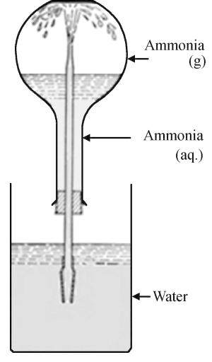
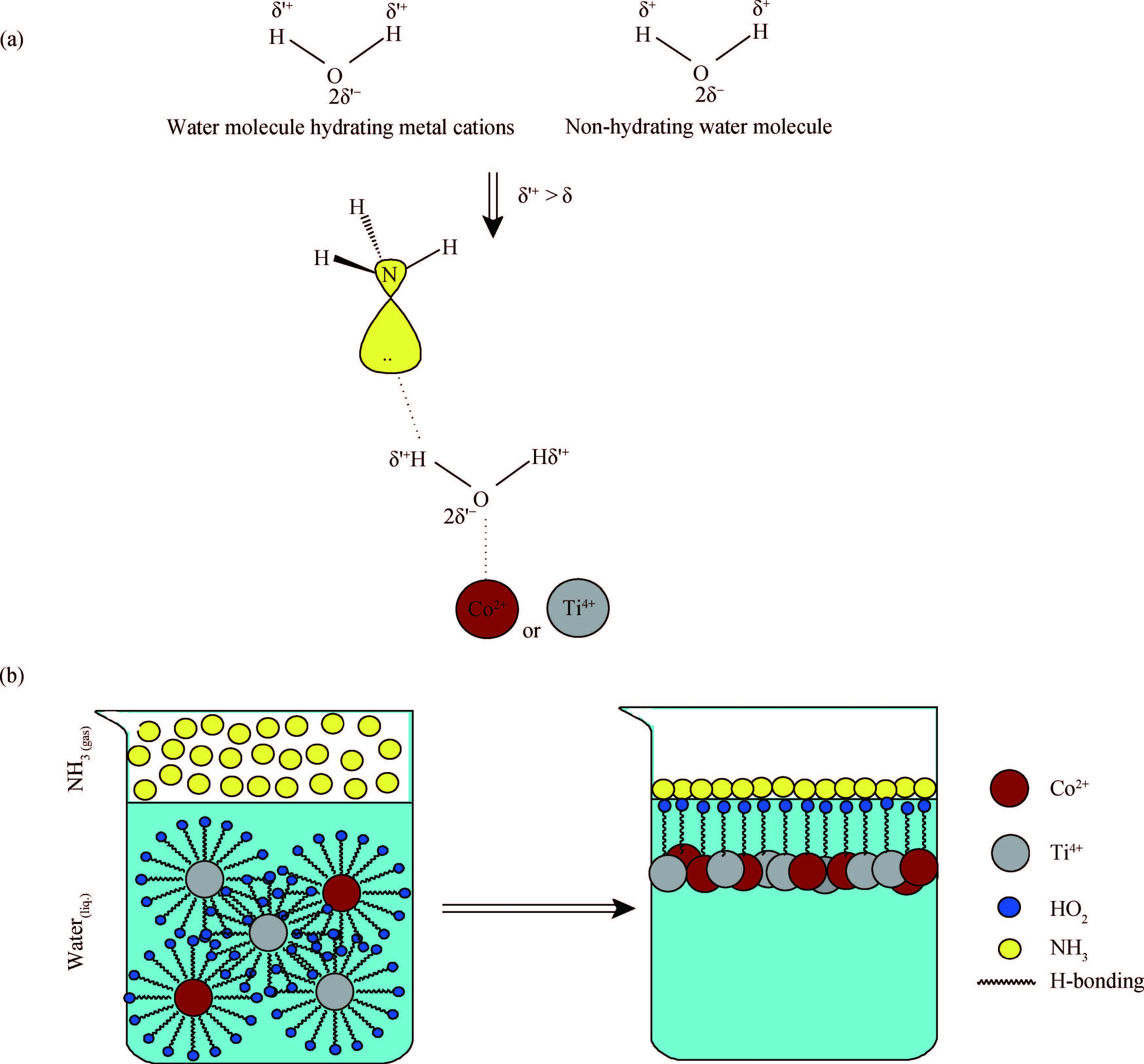
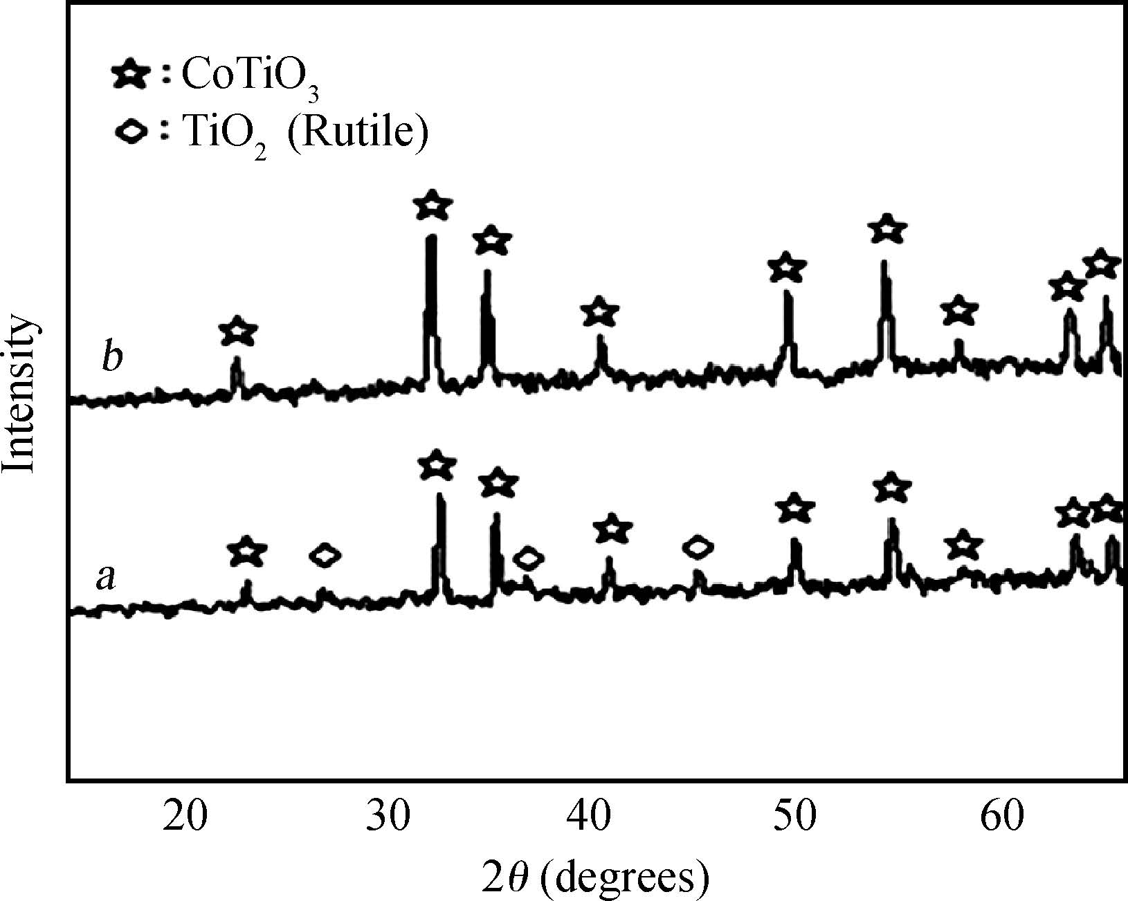
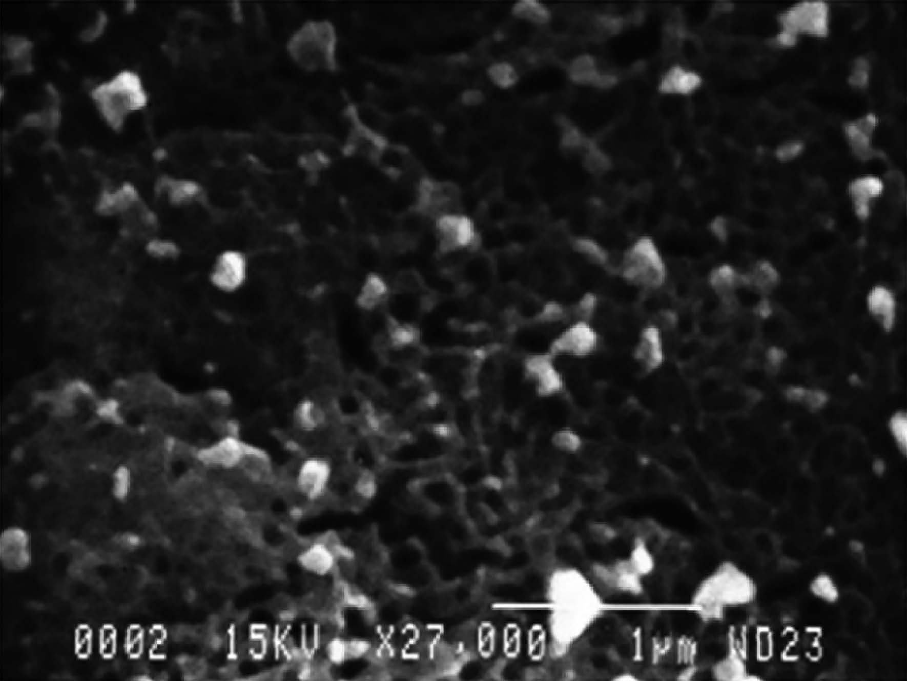
The theory of an "ammonia fountain" was developed to synthesize a CoTiO3 nanoporous matrix using a modified co-precipitation method at the interface of the aqueous solution and the saturated NH3 atmosphere. On the basis of this theory, for the first time, a new assumption was expanded to show the regular (re)arrangement of metal cations near to the surface of the solution. The morphology of the CoTiO3 phase was observed using SEM. The result indicates the nano-narrow formation of CoTiO3 particles. The size of the particles was calculated at about 27 nm. From the XRD patterns, the formation of cobalt titanate nanoparticles was confirmed.
J. Semicond.
2016, 37(2): 023003 doi: 10.1088/1674-4926/37/2/023003
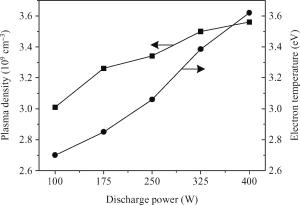
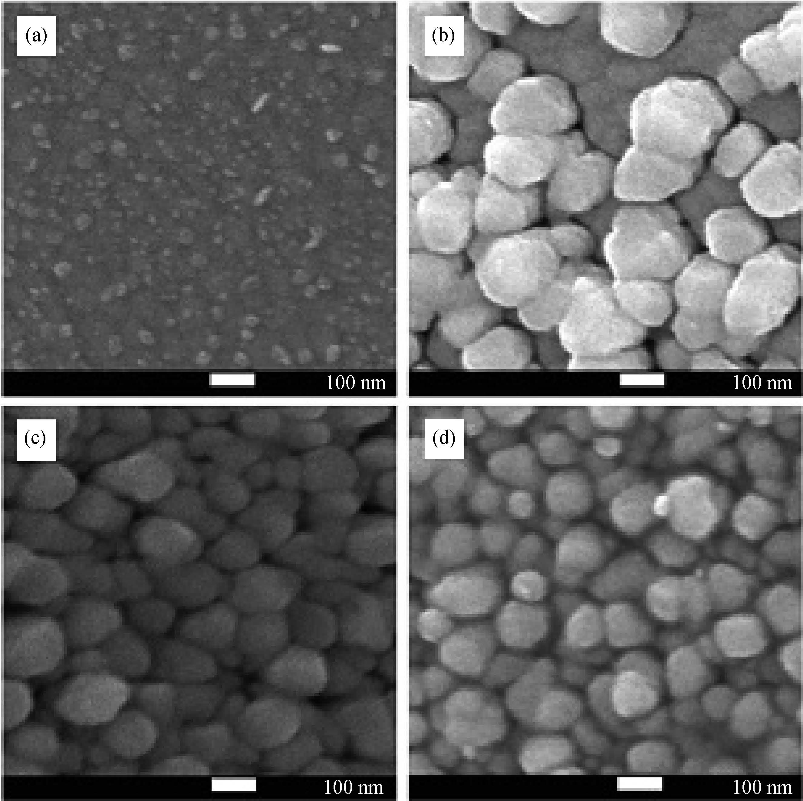
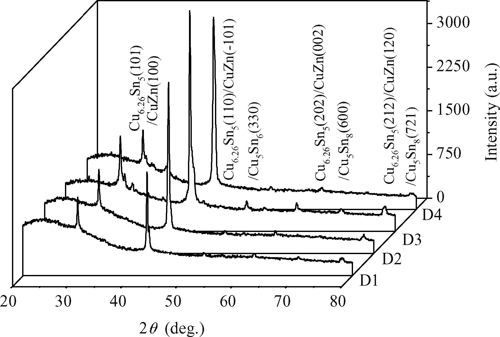
Cu-Zn-Sn (CZT) precursors were successfully prepared on glass substrate with the introduction of the assistant technology ICP (inductively coupled plasma) based on the conventional co-evaporation process. The deposition was performed with the substrate temperature at 220 ℃ and the chamber pressure at 6.5 × 10⁻² Pa. Argon plasma was investigated with a Langmuir probe. The plasma density and the electron temperature increased with the increasing of the discharge power. The impact of ICP discharge power on the structural and morphological properties of the CZT film were investigated with energy dispersive X-ray spectrometers (EDS), X-ray diffraction (XRD), and scanning electron microscopy (SEM). XRD and EDS were combined to investigate the structure of the film. The results show that Zn loss exists during the evaporation and the loss can be reduced by increasing the ICP discharge power. From the observation on the scanning electron microscope, the grain size becomes larger with argon plasma's assistance. The preparation of the Cu2ZnSnS4 (CZTS) film and the measured properties demonstrate that the ICP would optimize the growth of the film.


J. Semicond.
2016, 37(2): 023004 doi: 10.1088/1674-4926/37/2/023004

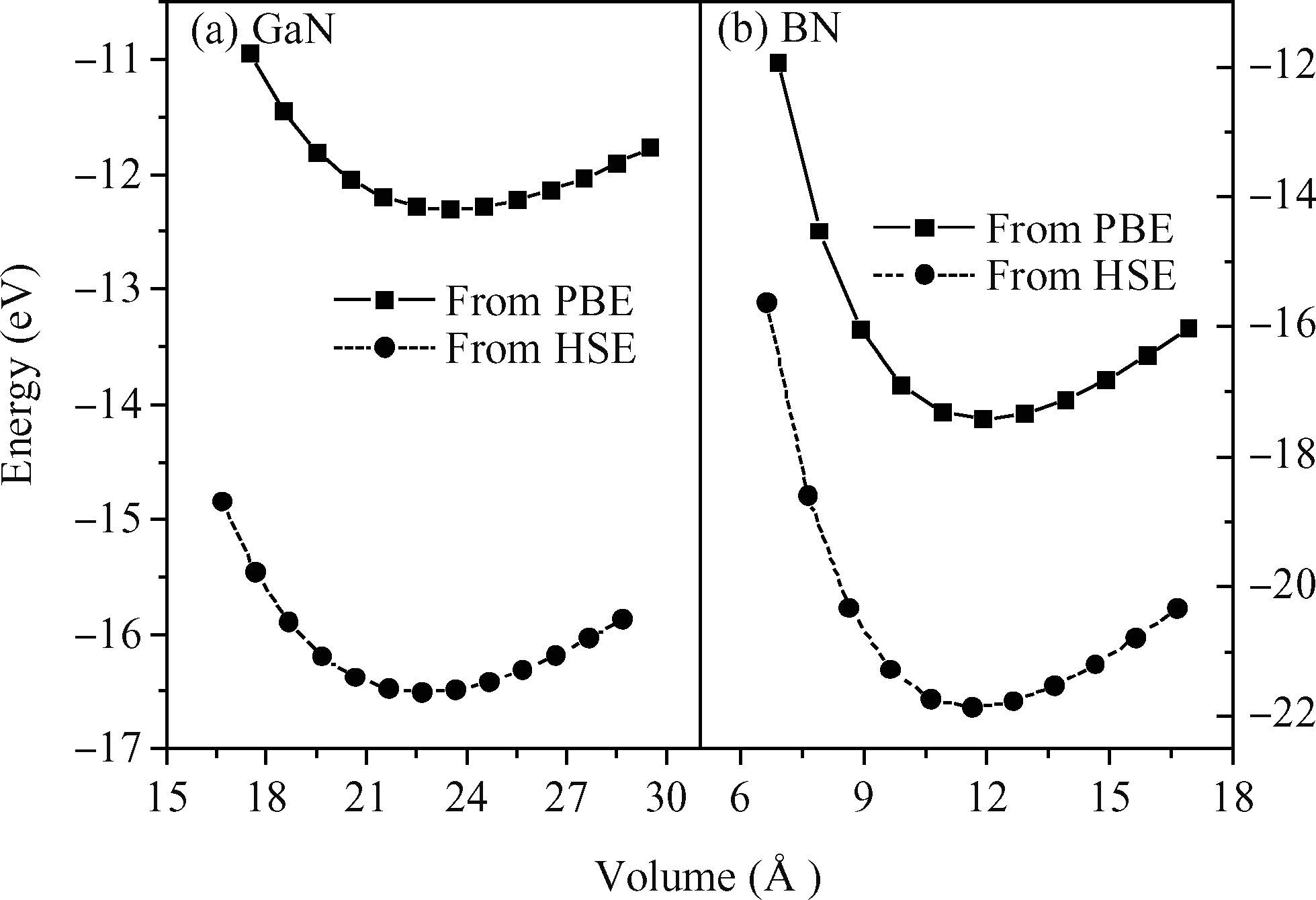
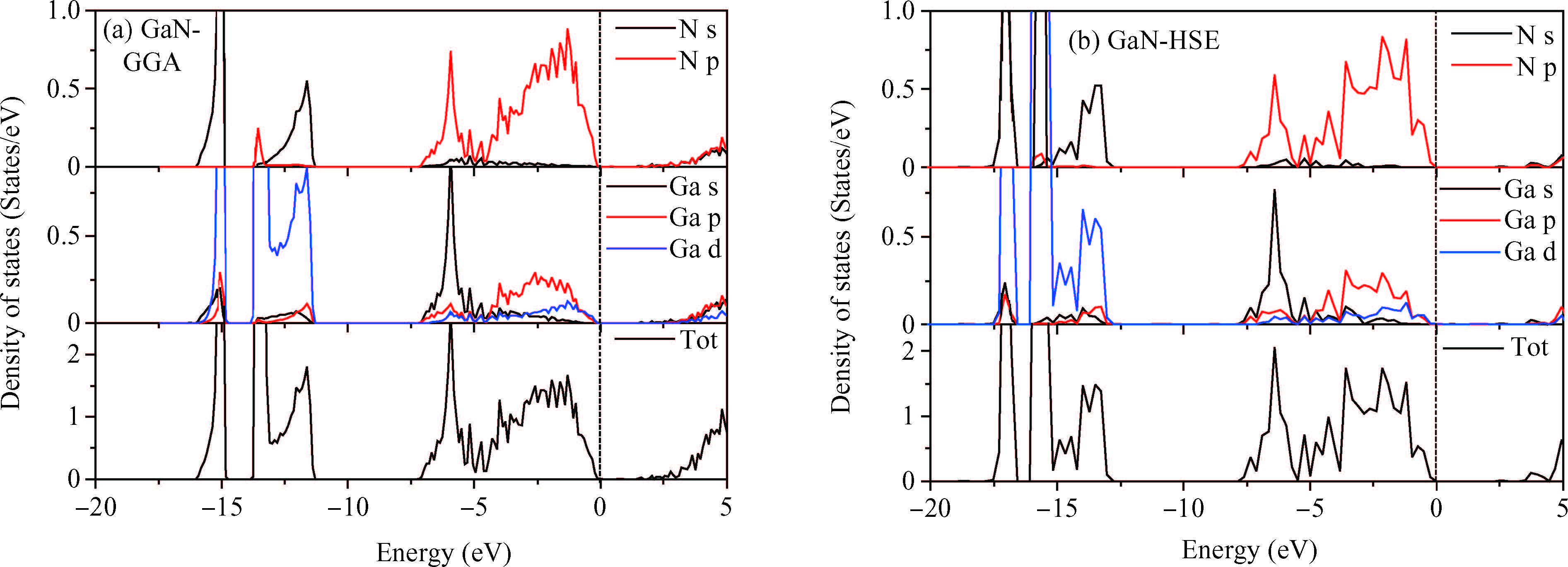
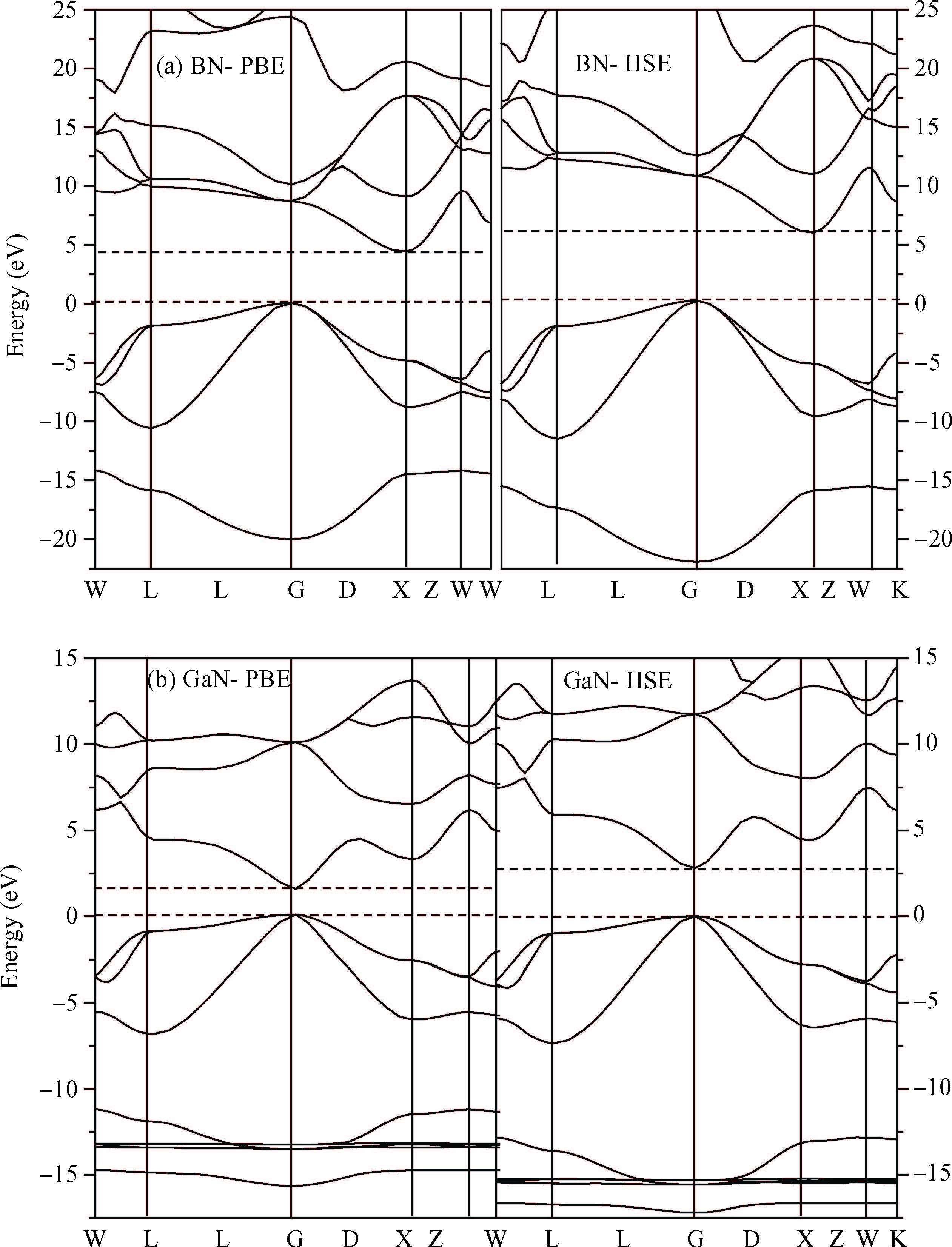
The electronic properties of zinc-blende BxGa1-xN alloys are comparatively investigated by employing both the Perdewe-Burkee-Ernzerhof generalized-gradient approximation (PBE-GGA) and the Heyd-Scuseria-Ernzerhof screened hybrid functional methods (HSE06). HSE06 reproduced much closer ground-state properties to experiments. Large and composition-dependent bowing parameters bΓ for the direct band gaps were obtained from both PBE and HSE06. The crossover composition where alloy switches from direct to indirect was predicted to occur at very similar x from PBE and HSE06. We can obtain direct gap BxGa1-xN with a gap value much larger than that of GaN by alloying x <0.557 boron into GaN.


J. Semicond.
2016, 37(2): 023005 doi: 10.1088/1674-4926/37/2/023005

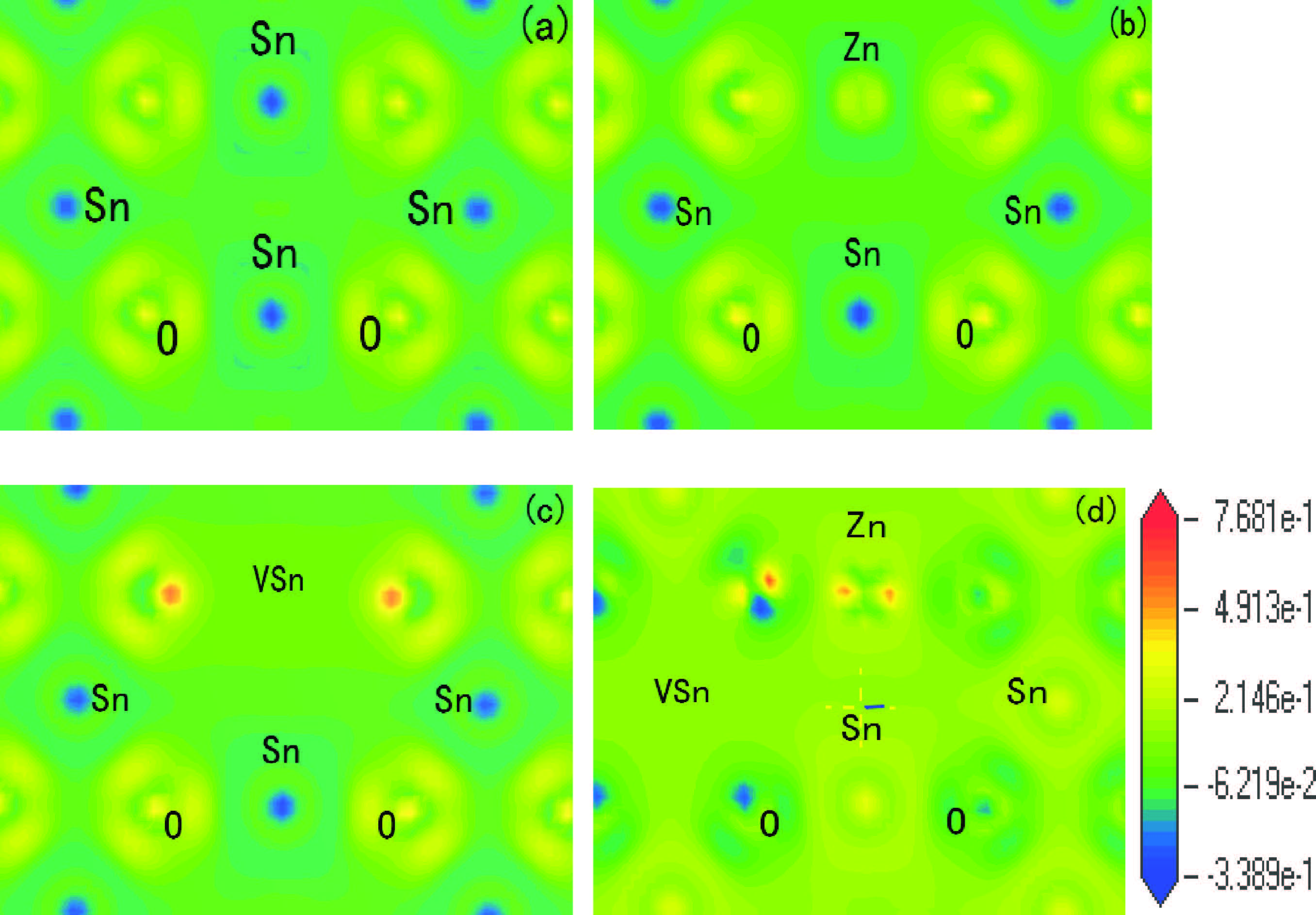
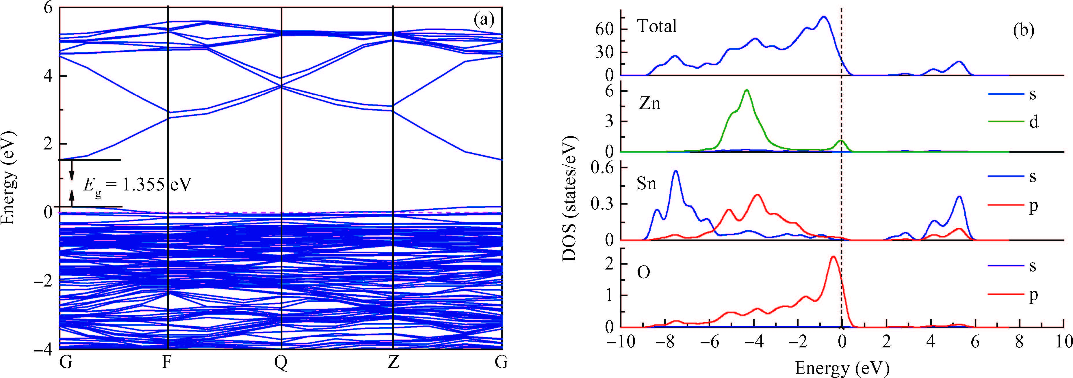
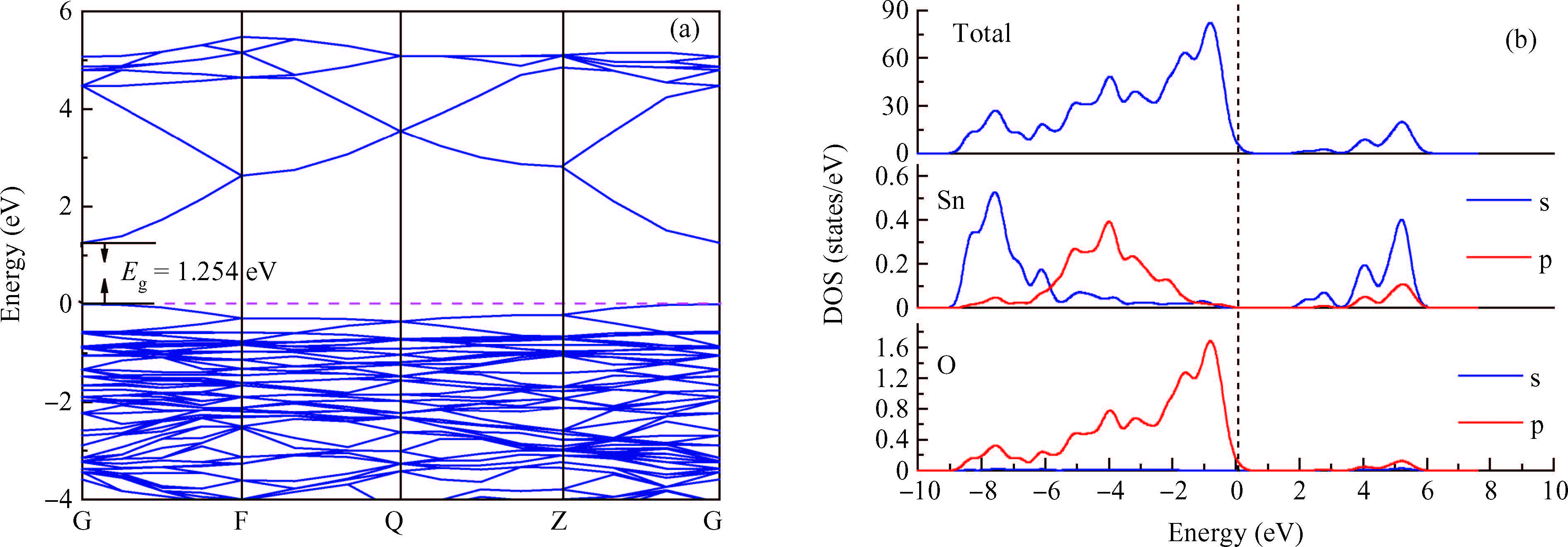
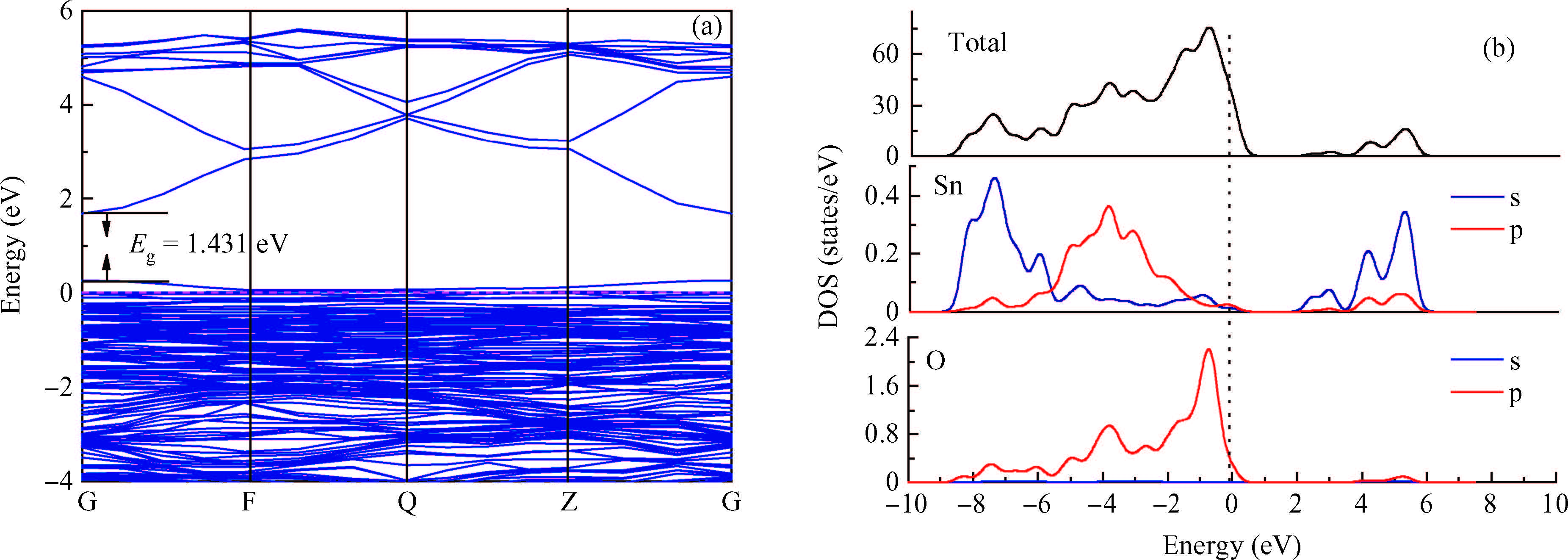
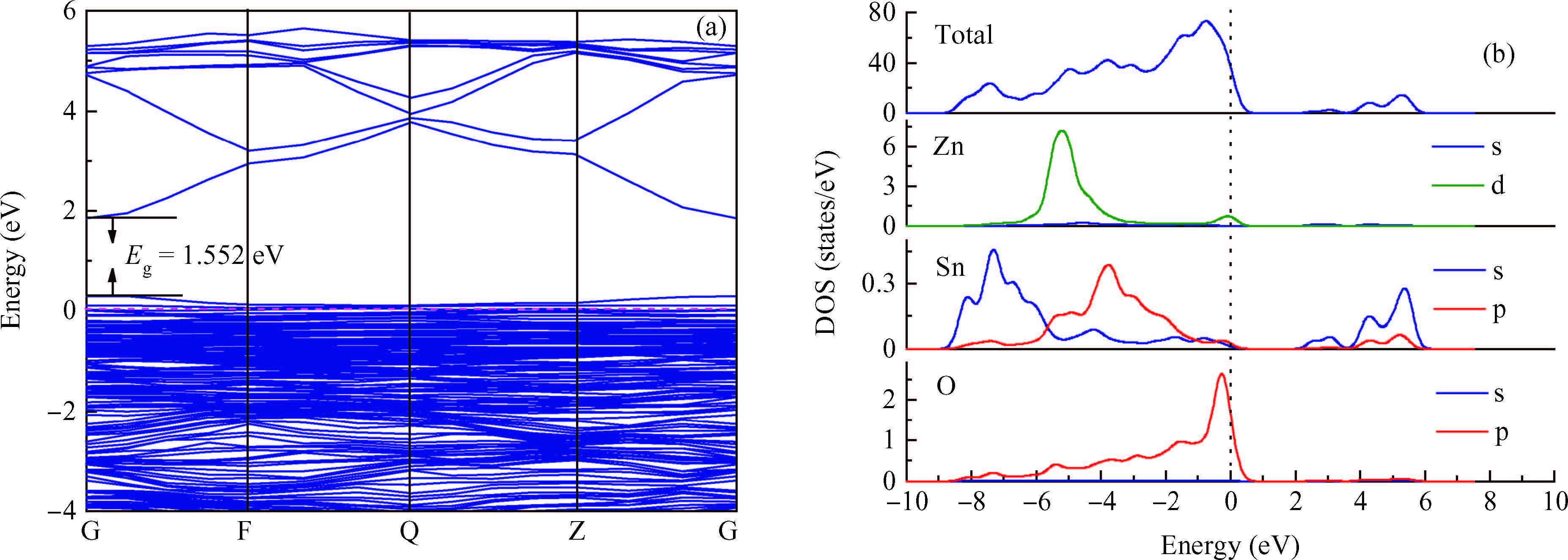
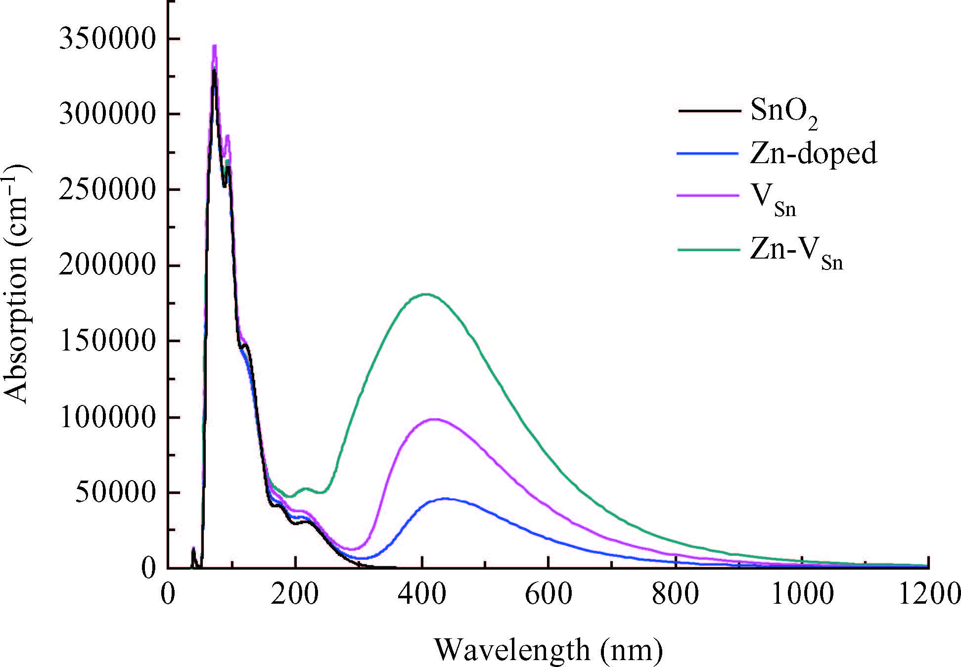
The electronic structures and optical properties of intrinsic SnO2, Zn-doped SnO2, SnO2 with Sn vacancy (VSn) and Zn-doped SnO2 with Sn vacancy are explored by using first-principles calculations. Zn-doped SnO2 is a p-type semiconductor material, whose Fermi level shifts into the valence band when Zn atoms substitute Sn atoms, and the unoccupied states on the top of the valence band come from Zn 3d and O 2p states. Sn vacancies increase the relative hole number of Zn-doped SnO2, which results in a possible increase in the conductivity of Zn-doped SnO2. The Zn-doped SnO2 shows distinct visible light absorption, the increased absorption can be seen apparently with the presence of Sn vacancies in the crystal, and the blue-shift of optical spectra can be observed.

J. Semicond.
2016, 37(2): 024001 doi: 10.1088/1674-4926/37/2/024001
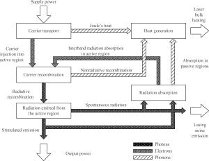
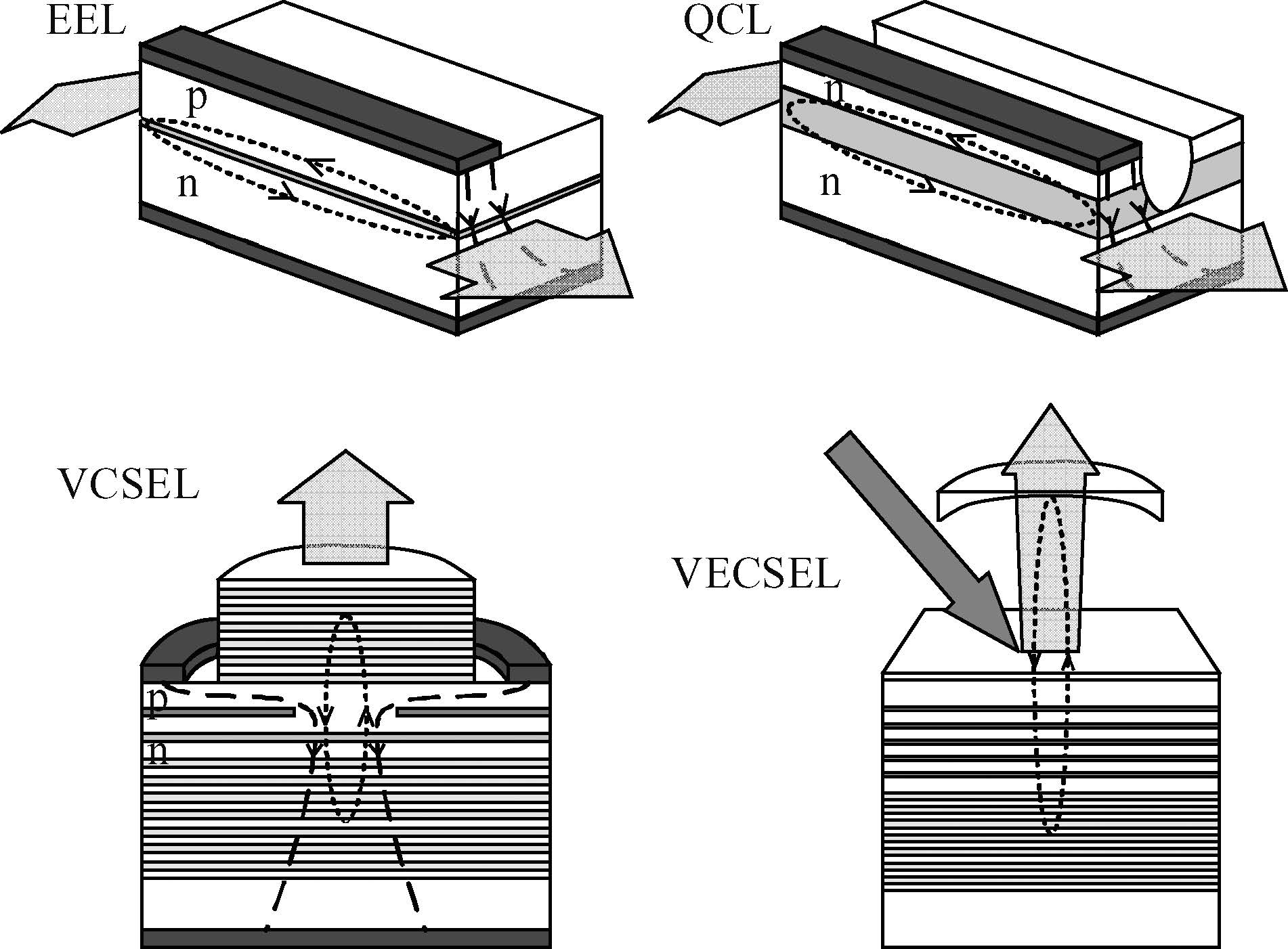
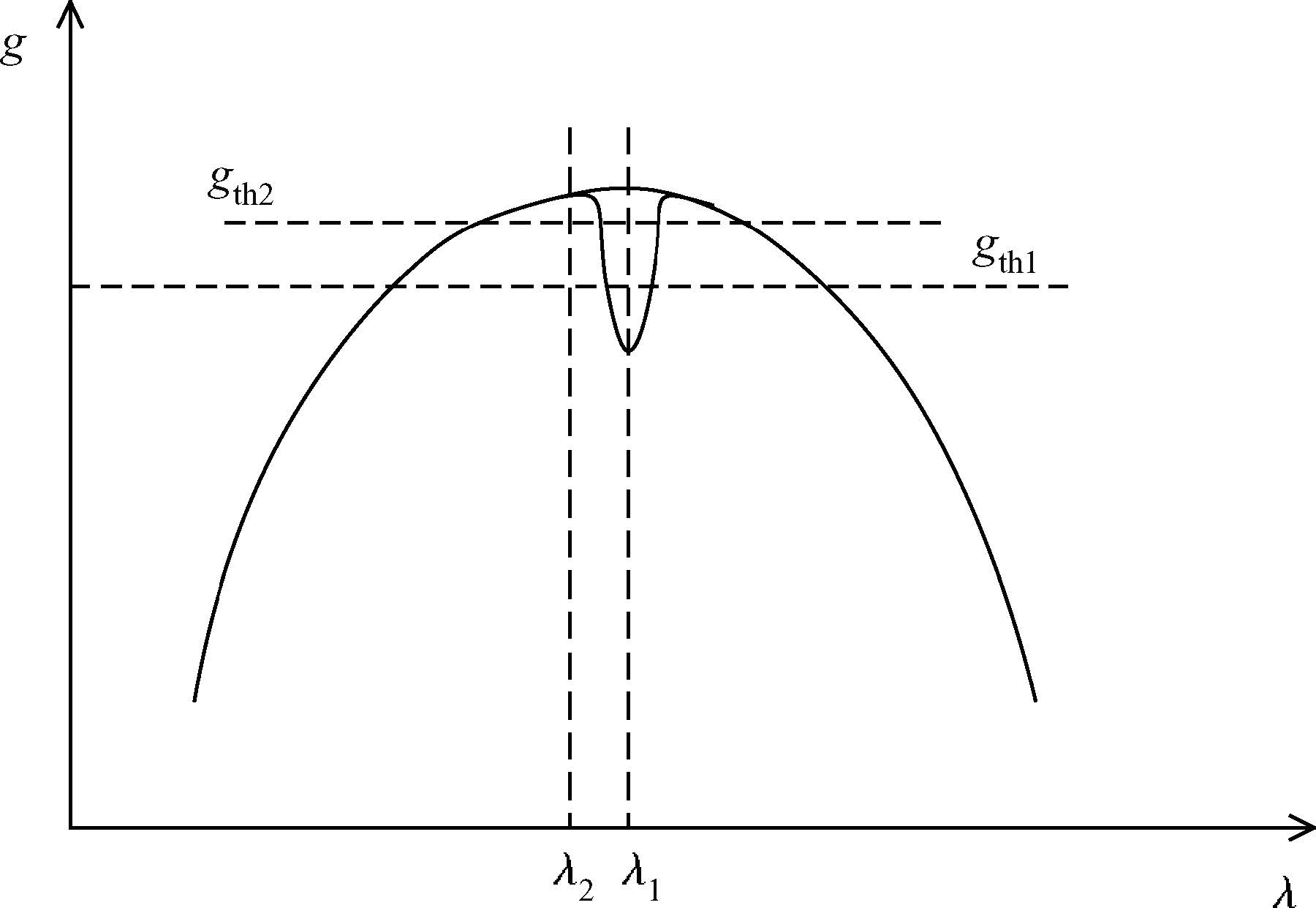
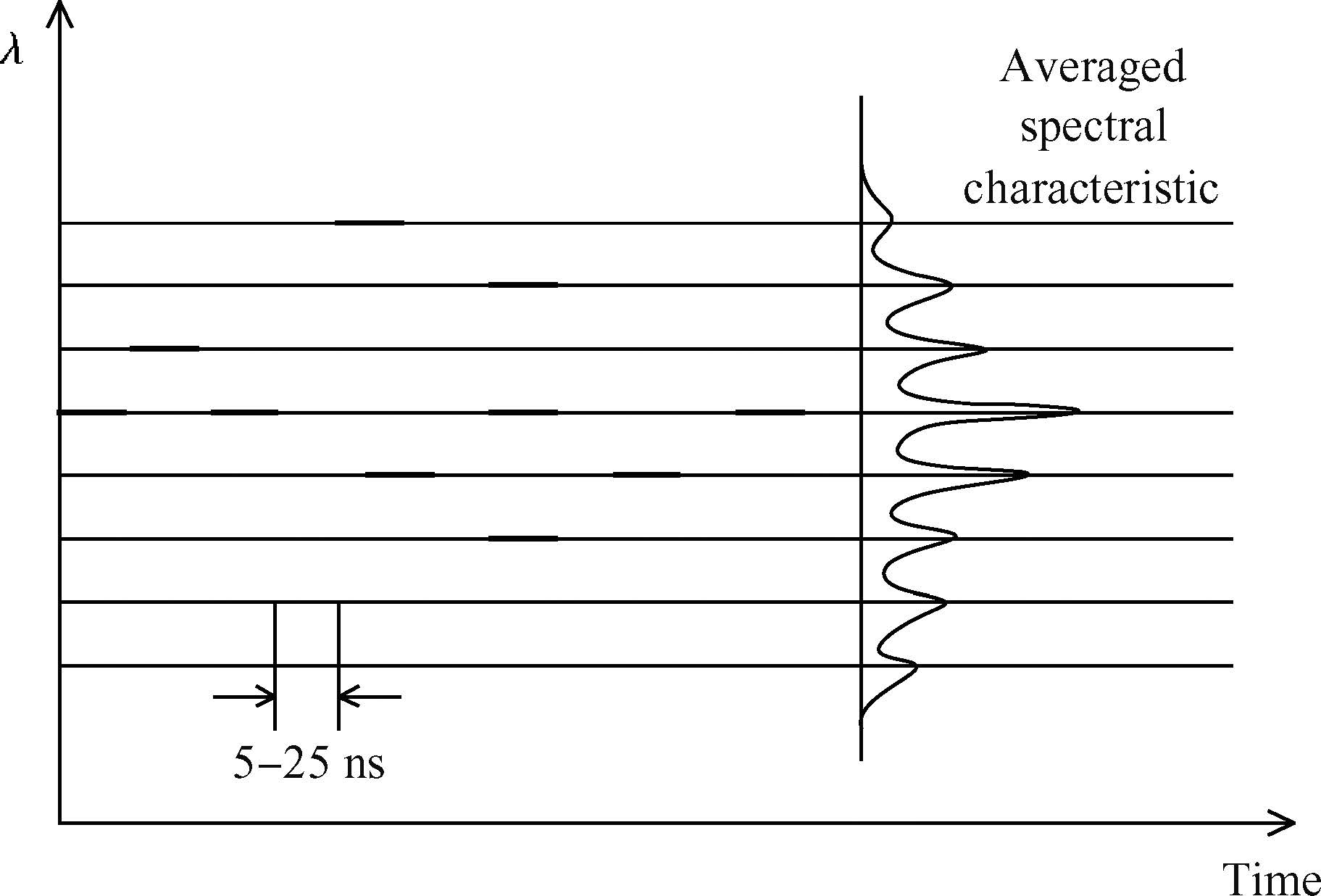
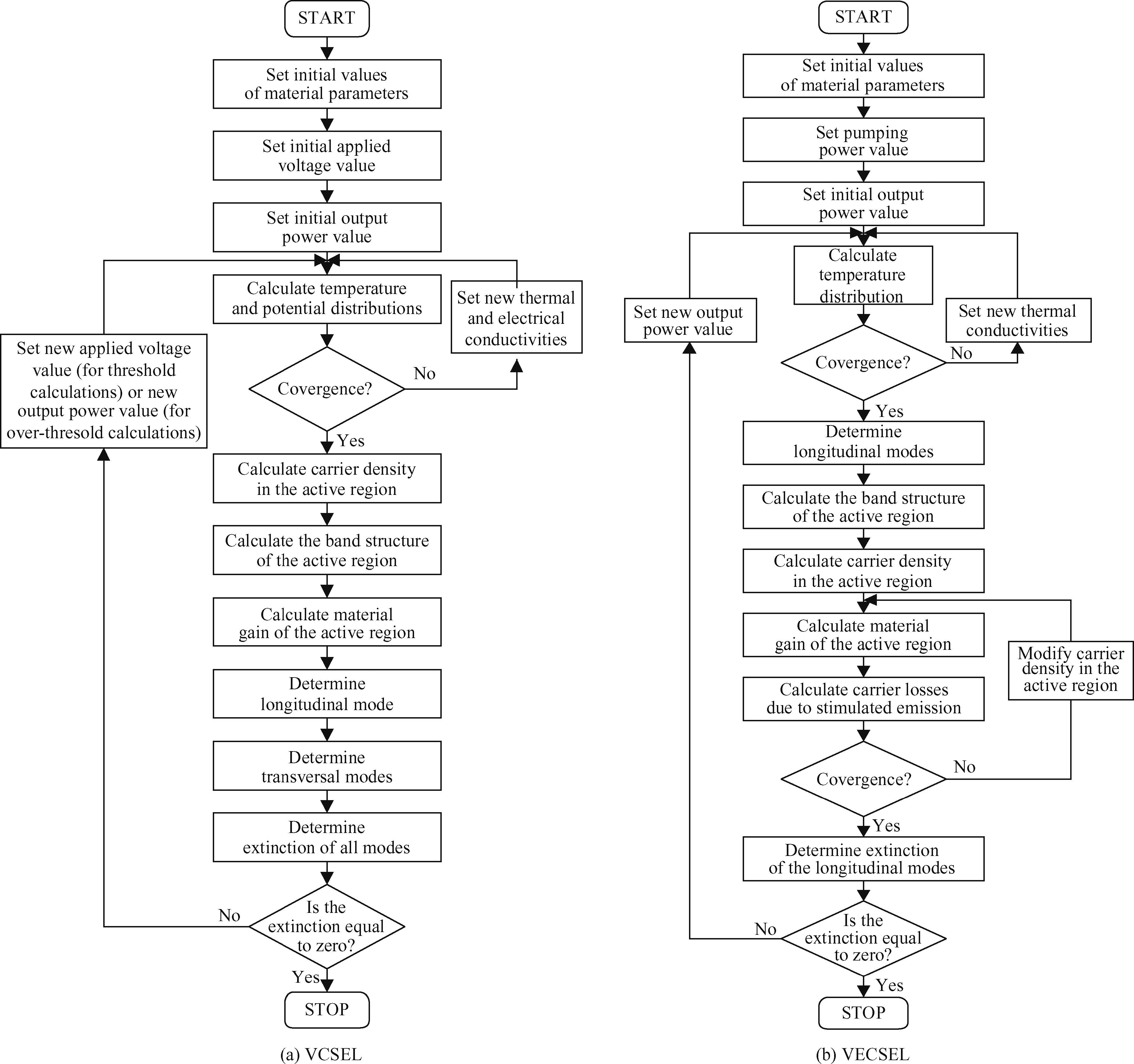
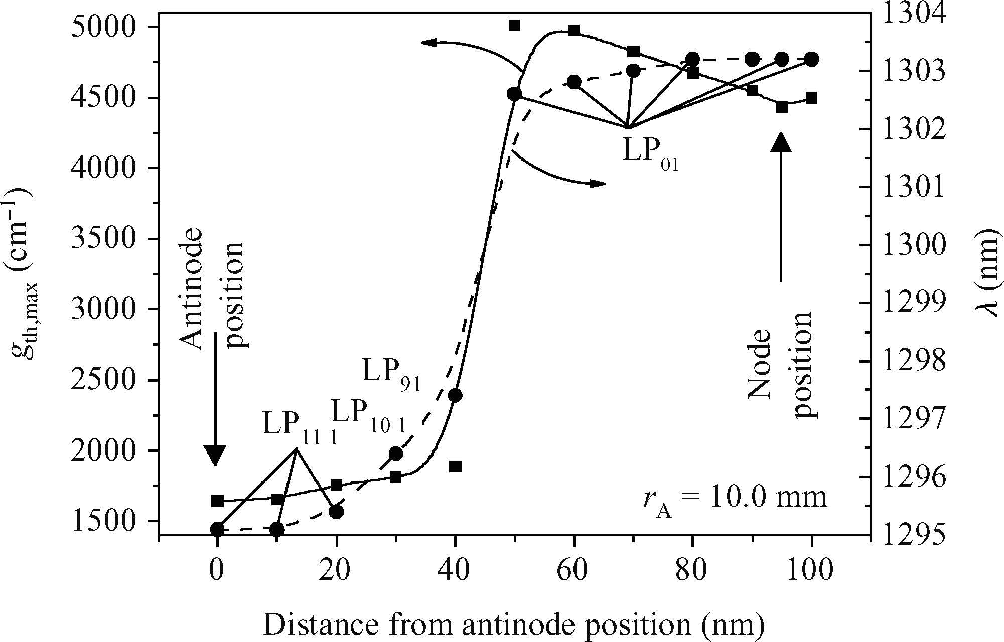
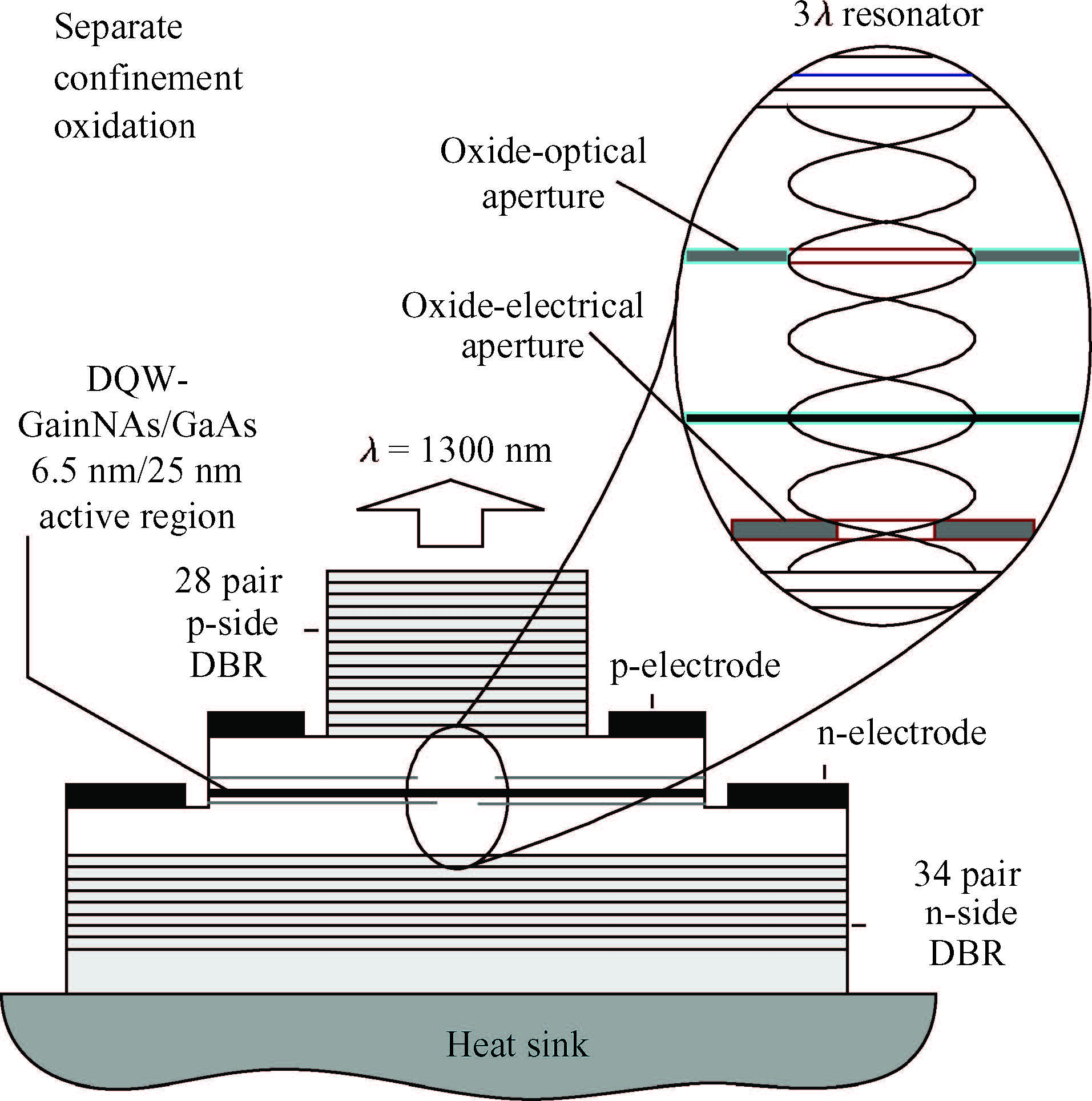
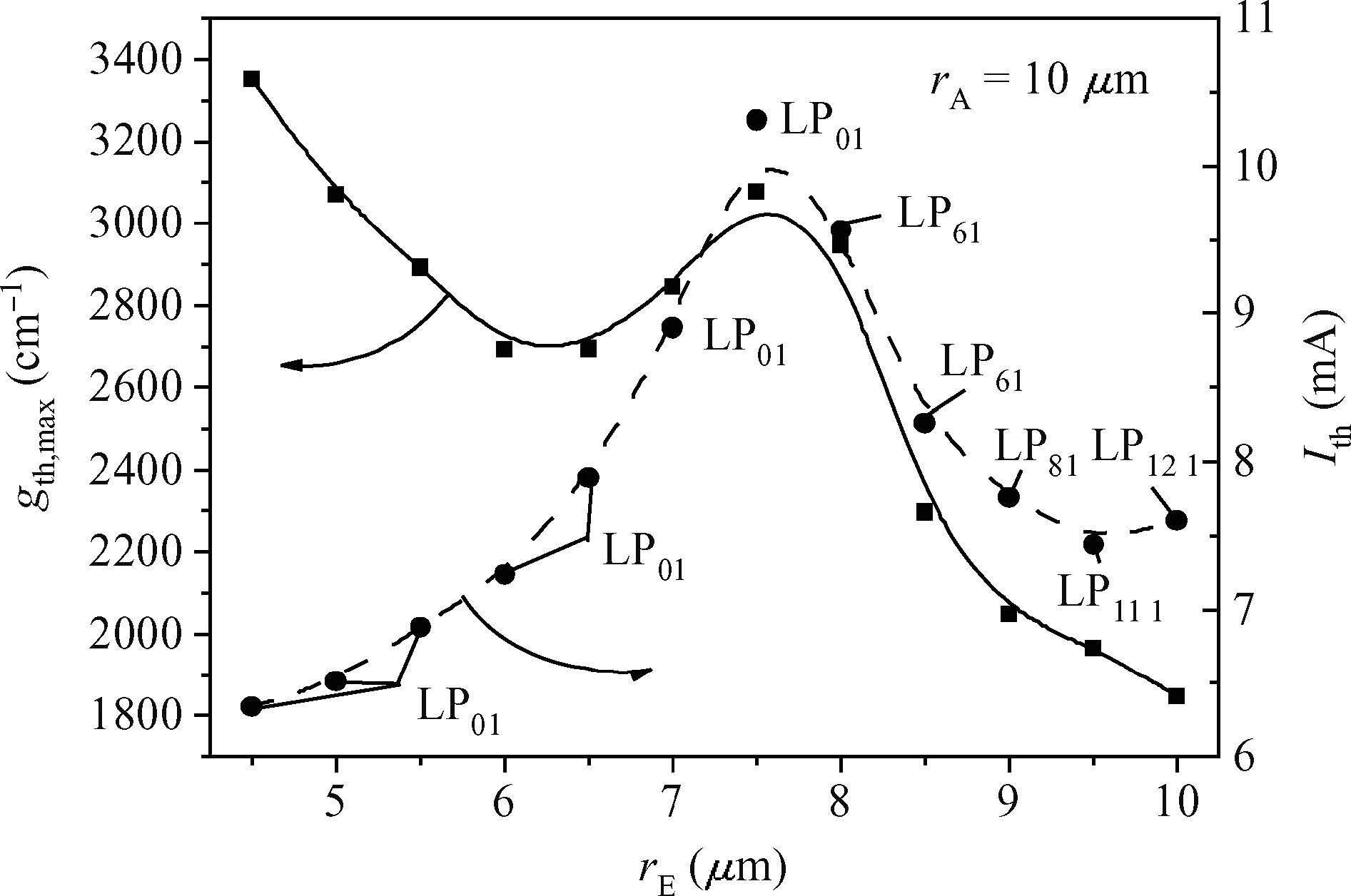
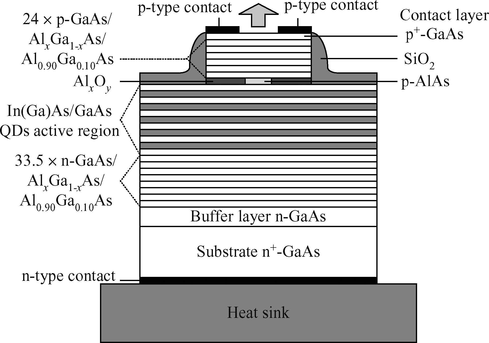
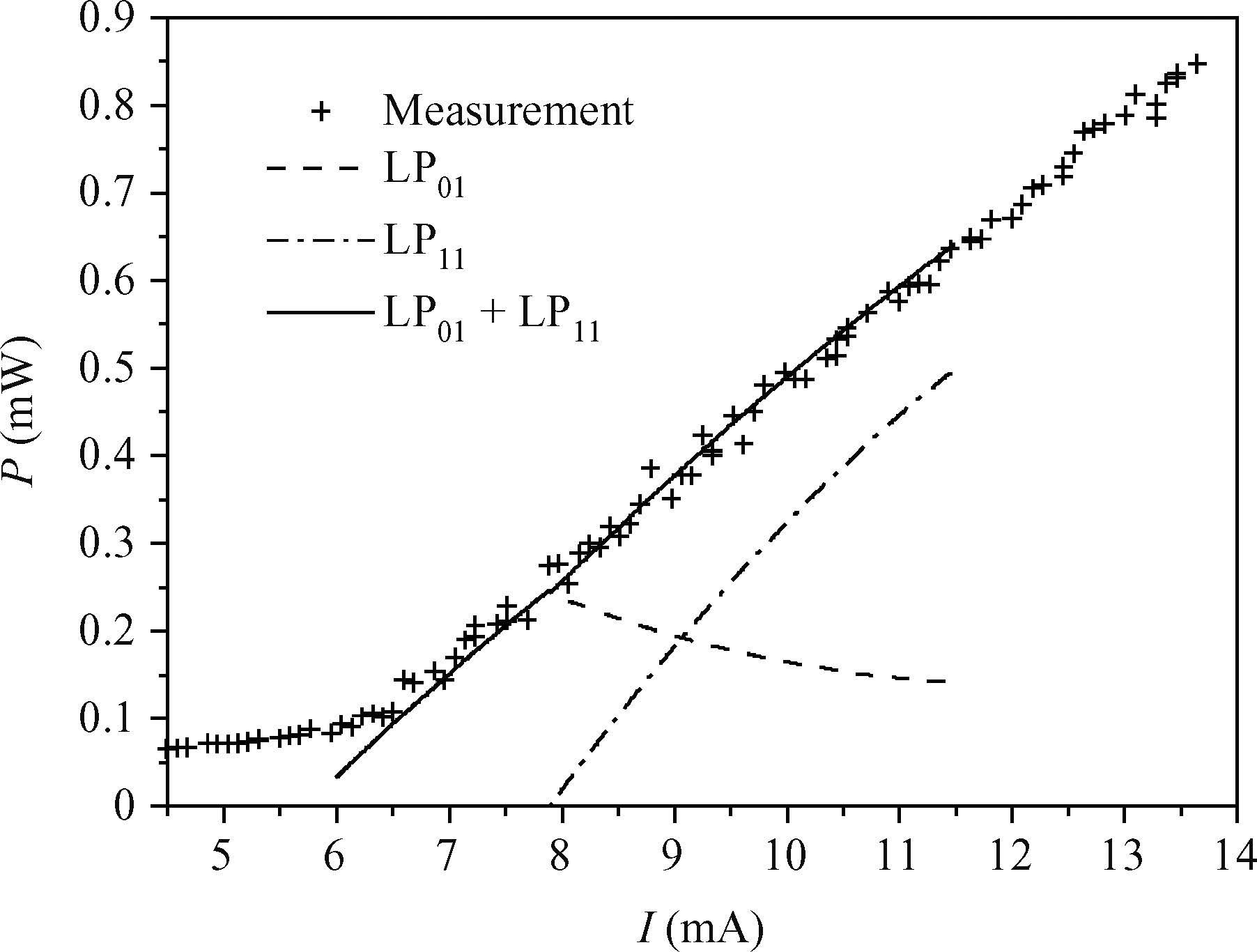
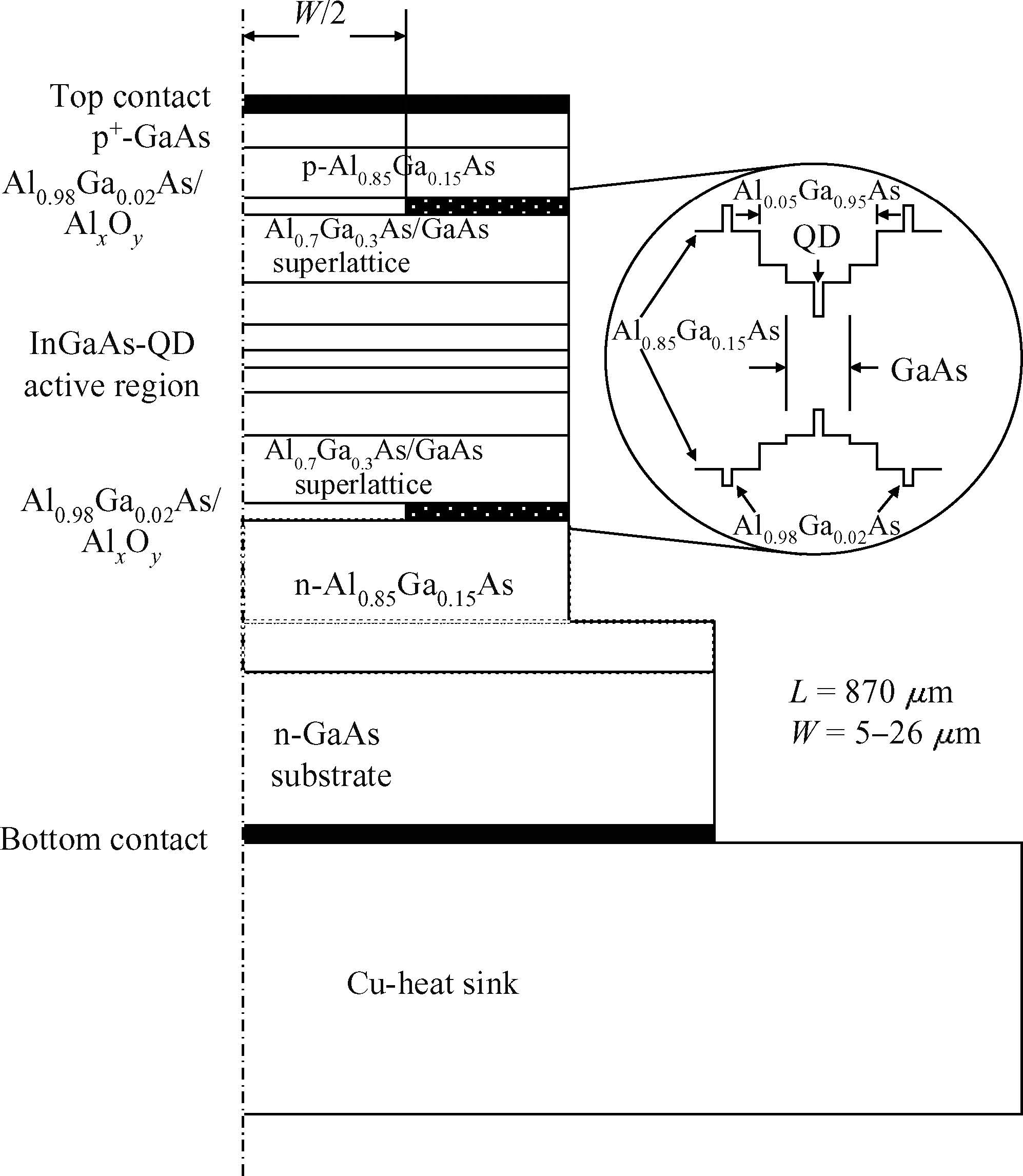
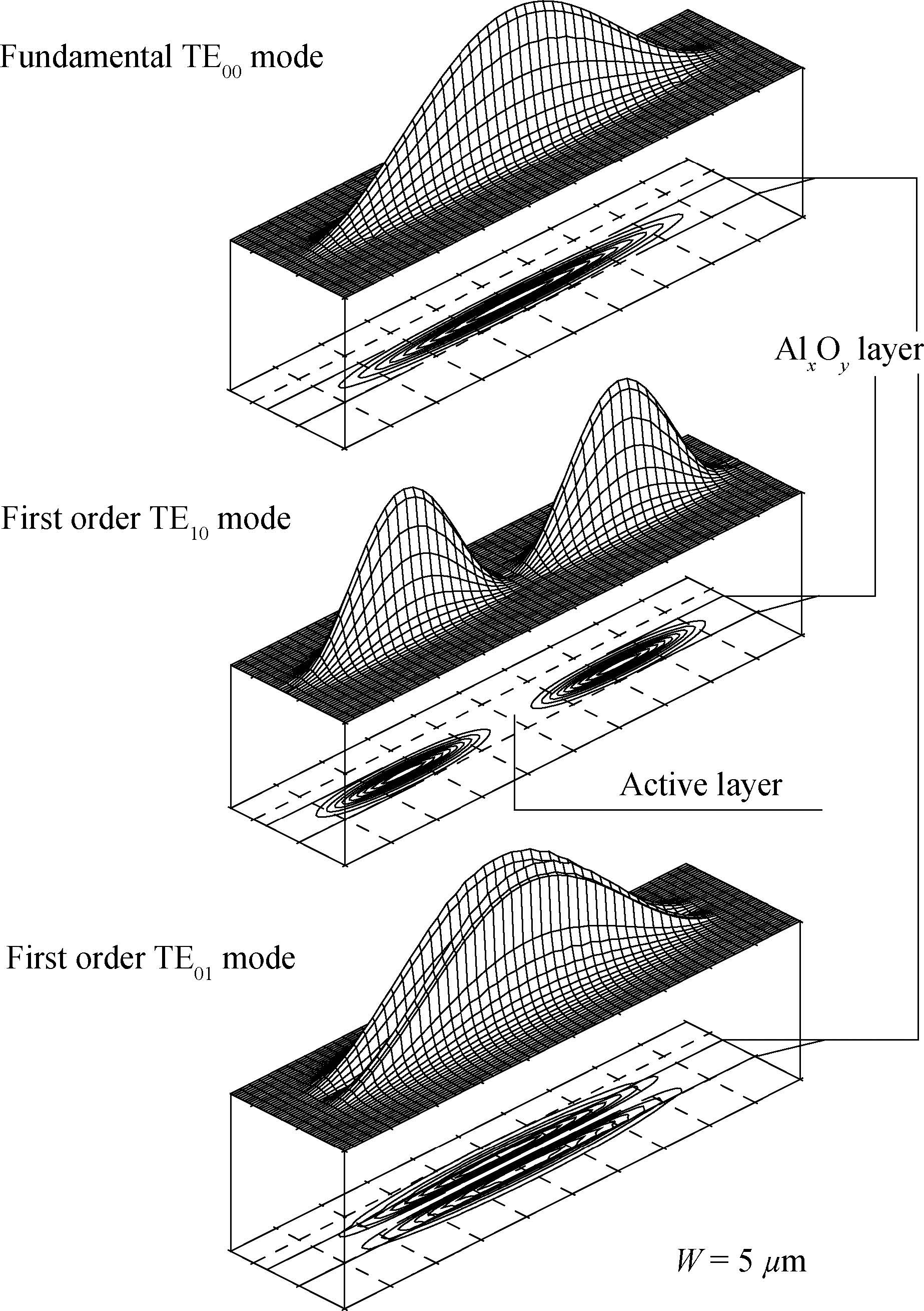
The fully self-consistent model of modern semiconductor lasers used to design their advanced structures and to understand more deeply their properties is given in the present paper. Operation of semiconductor lasers depends not only on many optical, electrical, thermal, recombination, and sometimes mechanical phenomena taking place within their volumes but also on numerous mutual interactions between these phenomena. Their experimental investigation is quite complex, mostly because of miniature device sizes. Therefore, the most convenient and exact method to analyze expected laser operation and to determine laser optimal structures for various applications is to examine the details of their performance with the aid of a simulation of laser operation in various considered conditions. Such a simulation of an operation of semiconductor lasers is presented in this paper in a full complexity of all mutual interactions between the above individual physical processes. In particular, the hole-burning effect has been discussed. The impacts on laser performance introduced by oxide apertures (their sizes and localization) have been analyzed in detail. Also, some important details concerning the operation of various types of semiconductor lasers are discussed. The results of some applications of semiconductor lasers are shown for successive laser structures.


J. Semicond.
2016, 37(2): 024002 doi: 10.1088/1674-4926/37/2/024002

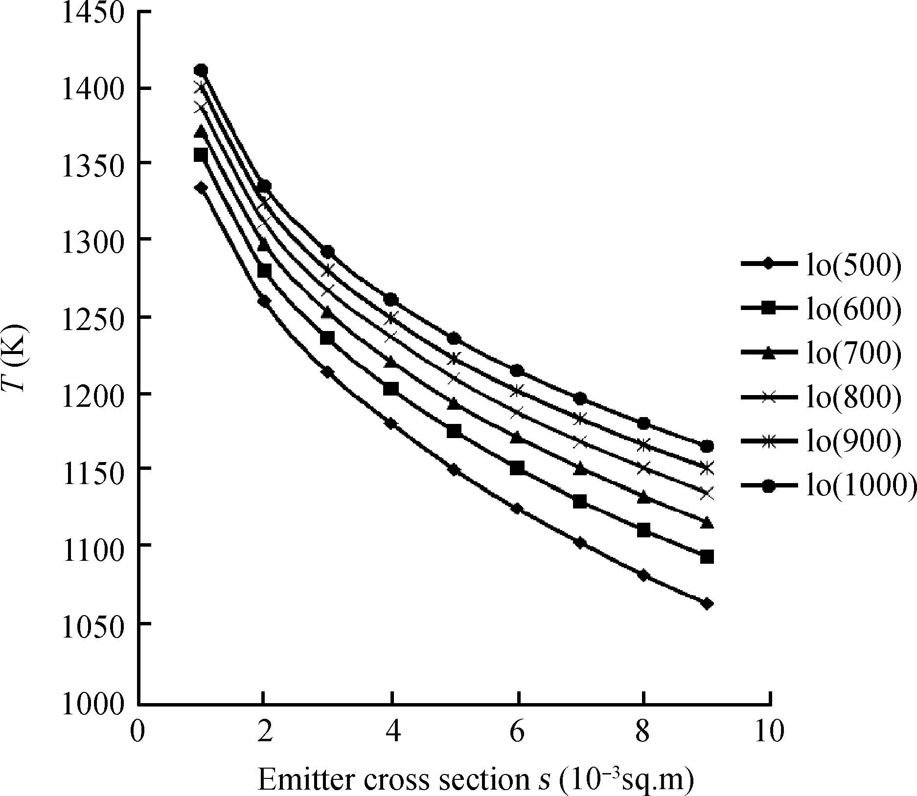
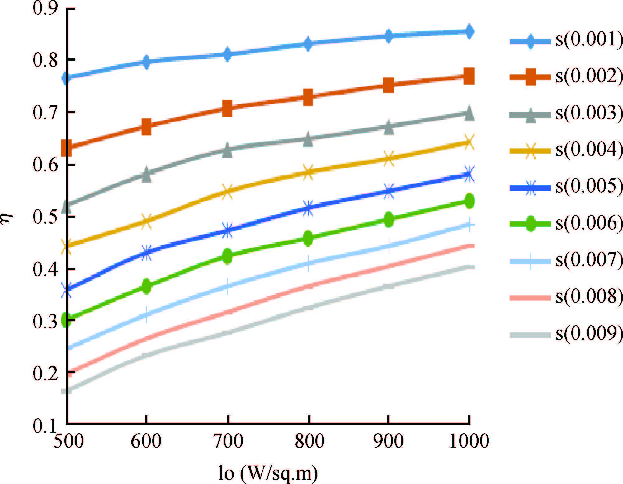
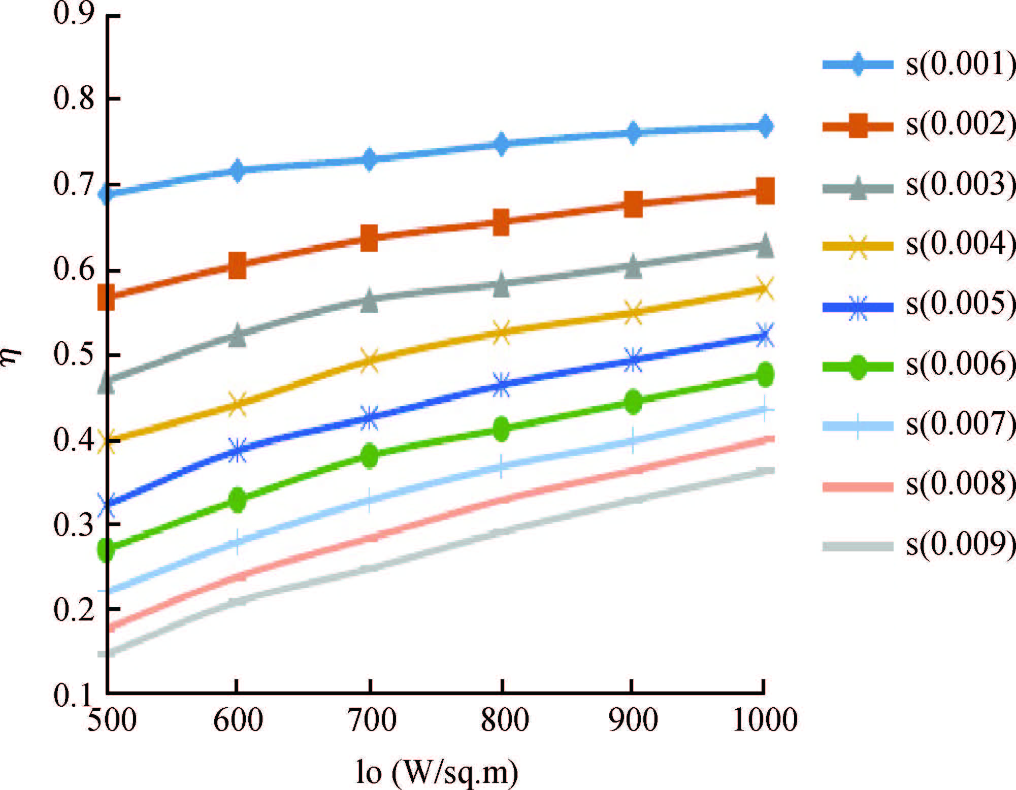
We consider the energy dynamics of the power generation from the sun when the solar energy is concentrated on to the emitter of a thermo-electronic converter with the help of a parabolic mirror. We use the modified Richardson-Dushman equation. The emitter cross section is assumed to be exactly equal to the focused area at a height h from the base of the mirror to prevent loss of efficiency. We report the variation of output power with solar insolation, height h, reflectivity of the mirror, and anode temperature, initially assuming that there is no space charge effect. Our methodology allows us to predict the temperature at which the anode must be cooled in order to prevent loss of efficiency of power conversion. Novel ways of tackling the space charge problem have been discussed. The space charge effect is modeled through the introduction of a parameter f (0 < f <1) in the thermos-electron emission equation. We find that the efficiency of the power conversion depends on solar insolation, height h, apart from radii R of the concentrator aperture and emitter, and the collector material properties. We have also considered solar thermos electronic power conversion by using single atom-layer graphene as an emitter.


J. Semicond.
2016, 37(2): 024003 doi: 10.1088/1674-4926/37/2/024003
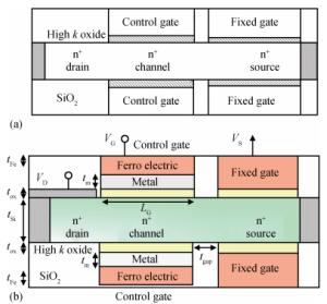
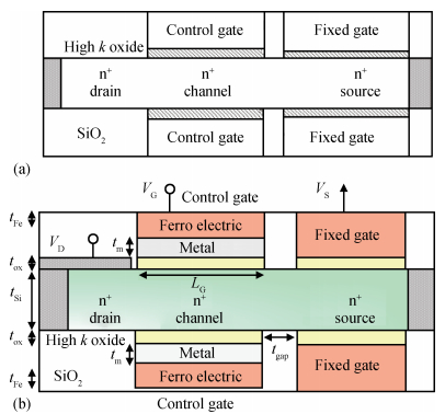
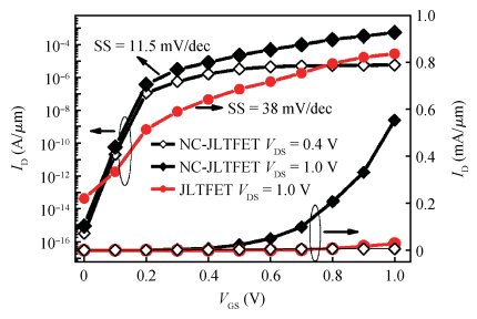
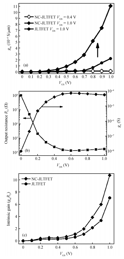
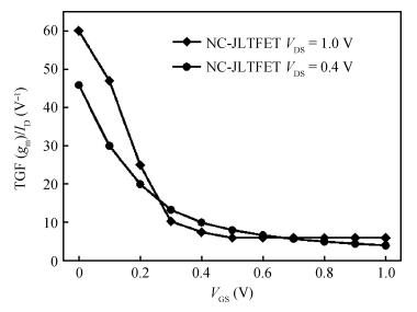
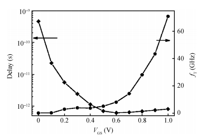
We investigate the transient behavior of an n-type double gate negative capacitance junctionless tunnel field effect transistor (NC-JLTFET). The structure is realized by using the work-function engineering of metal electrodes over a heavily doped n+ silicon channel and a ferroelectric gate stack to get negative capacitance behavior. The positive feedback in the electric dipoles of ferroelectric materials results in applied gate bias boosting. Various device transient parameters viz. transconductance, output resistance, output conductance, intrinsic gain, intrinsic gate delay, transconductance generation factor and unity gain frequency are analyzed using ac analysis of the device. To study the impact of the work-function variation of control and source gate on device performance, sensitivity analysis of the device has been carried out by varying these parameters. Simulation study reveals that it preserves inherent advantages of charge-plasma junctionless structure and exhibits improved transient behavior as well.
J. Semicond.
2016, 37(2): 024004 doi: 10.1088/1674-4926/37/2/024004
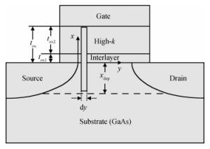
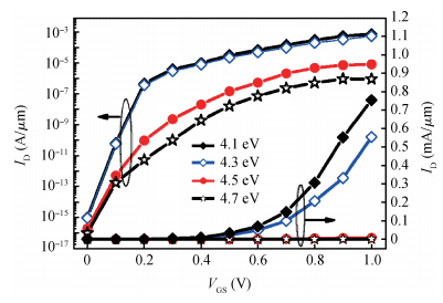
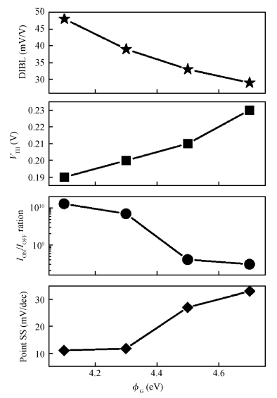
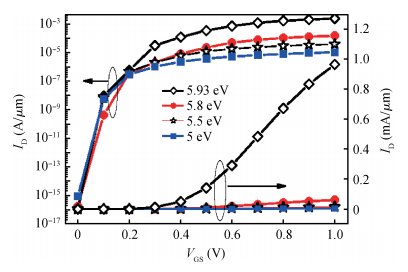
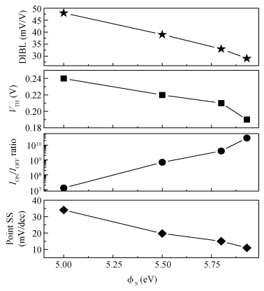
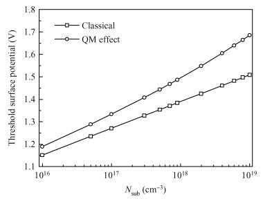
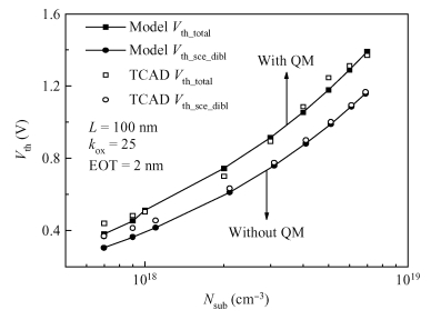
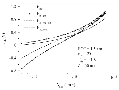
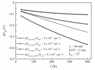
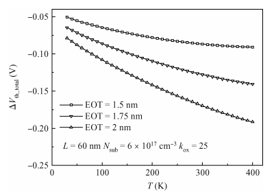
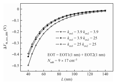
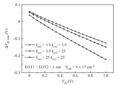
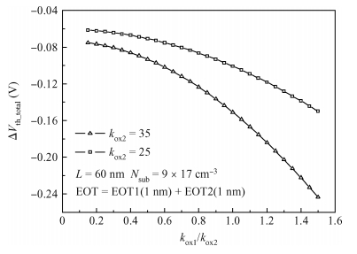
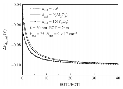
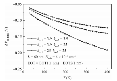
A threshold-voltage model for a stacked high-k gate dielectric GaAs MOSFET is established by solving a two-dimensional Poisson's equation in channel and considering the short-channel, DIBL and quantum effects. The simulated results are in good agreement with the Silvaco TCAD data, confirming the correctness and validity of the model. Using the model, impacts of structural and physical parameters of the stack high-k gate dielectric on the threshold-voltage shift and the temperature characteristics of the threshold voltage are investigated. The results show that the stacked gate dielectric structure can effectively suppress the fringing-field and DIBL effects and improve the threshold and temperature characteristics, and on the other hand, the influence of temperature on the threshold voltage is overestimated if the quantum effect is ignored.

J. Semicond.
2016, 37(2): 024005 doi: 10.1088/1674-4926/37/2/024005
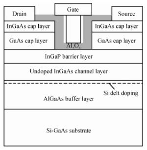
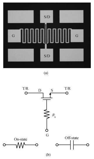
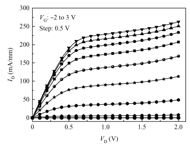
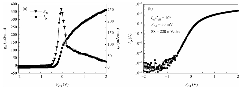
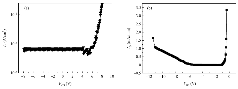
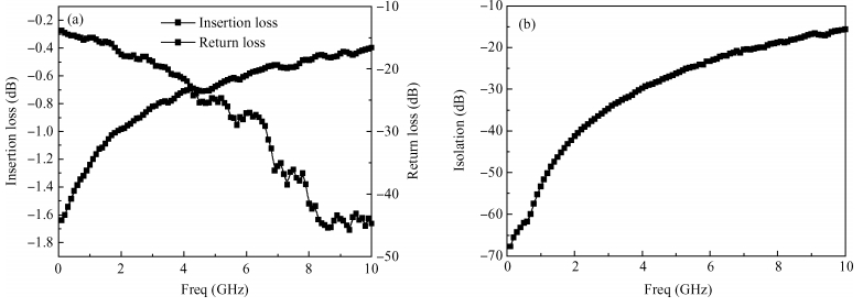
A novel radio frequency (RF) switch device has been successfully fabricated using InGaAs metal-oxide-semiconductor field-effect transistor (MOSFET) technology. The device showed drain saturation currents of 250 mA/mm, a maximum transconductance of 370 mS/mm, a turn-on resistance of 0.72 mΩ · mm2 and a drain current on-off (Ion/Ioff) ratio of 1 × 10⁶. The maximum handling power of on-state of 533 mW/mm and off-state of 3667 mW/mm is obtained. The proposed In0.4Ga0.6As MOSFET RF switch showed an insertion loss of less than 1.8 dB and an isolation of better than 20 dB in the frequency range from 0.1 to 7.5 GHz. The lowest insertion loss and the highest isolation can reach 0.27 dB and more than 68 dB respectively. This study demonstrates that the InGaAs MOSFET technology has a great potential for RF switch application.

J. Semicond.
2016, 37(2): 024006 doi: 10.1088/1674-4926/37/2/024006
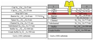
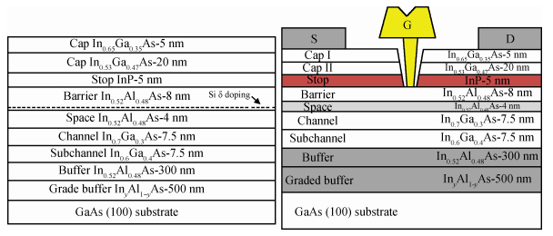
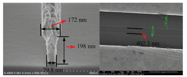
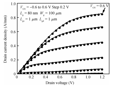
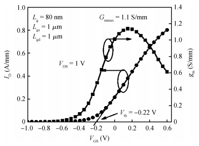
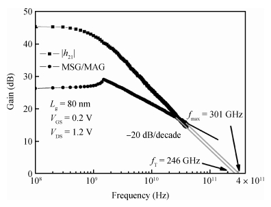
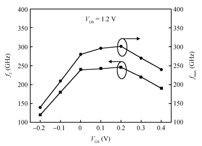
An 80-nm gate length metamorphic high electron mobility transistor (mHEMT) on a GaAs substrate with high indium composite compound-channels In0.7Ga0.3As/In0.6Ga0.4As and an optimized grade buffer scheme is presented. High 2-DEG Hall mobility values of 10200 cm2/(V· s) and a sheet density of 3.5 × 1012 cm-2 at 300 K have been achieved. The device's T-shaped gate was made by utilizing a simple three layers electron beam resist, instead of employing a passivation layer for the T-share gate, which is beneficial to decreasing parasitic capacitance and parasitic resistance of the gate and simplifying the device manufacturing process. The ohmic contact resistance Rc is 0.2 Ω ·mm when using the same metal system with the gate (Pt/Ti/Pt/Au), which reduces the manufacturing cycle of the device. The mHEMT device demonstrates excellent DC and RF characteristics. The peak extrinsic transconductance of 1.1 S/mm and the maximum drain current density of 0.86 A/mm are obtained. The unity current gain cut-off frequency (fT) and the maximum oscillation frequency (fmax) are 246 and 301 GHz, respectively.
J. Semicond.
2016, 37(2): 024007 doi: 10.1088/1674-4926/37/2/024007
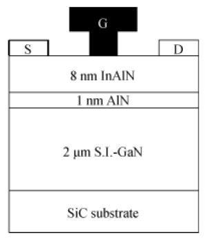
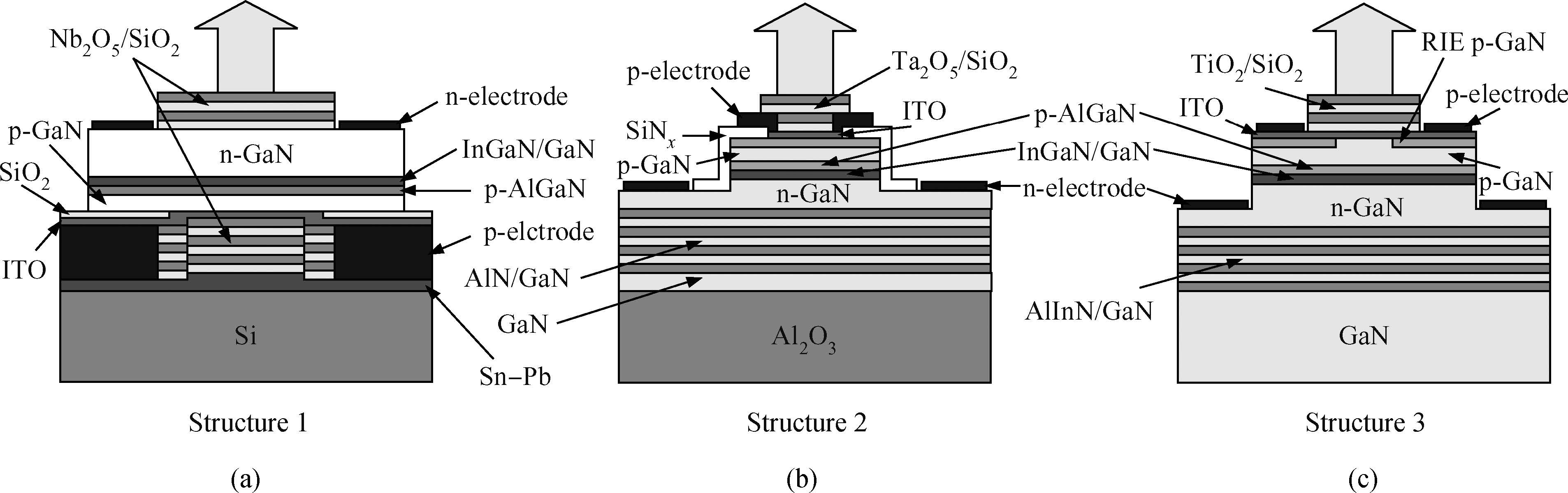
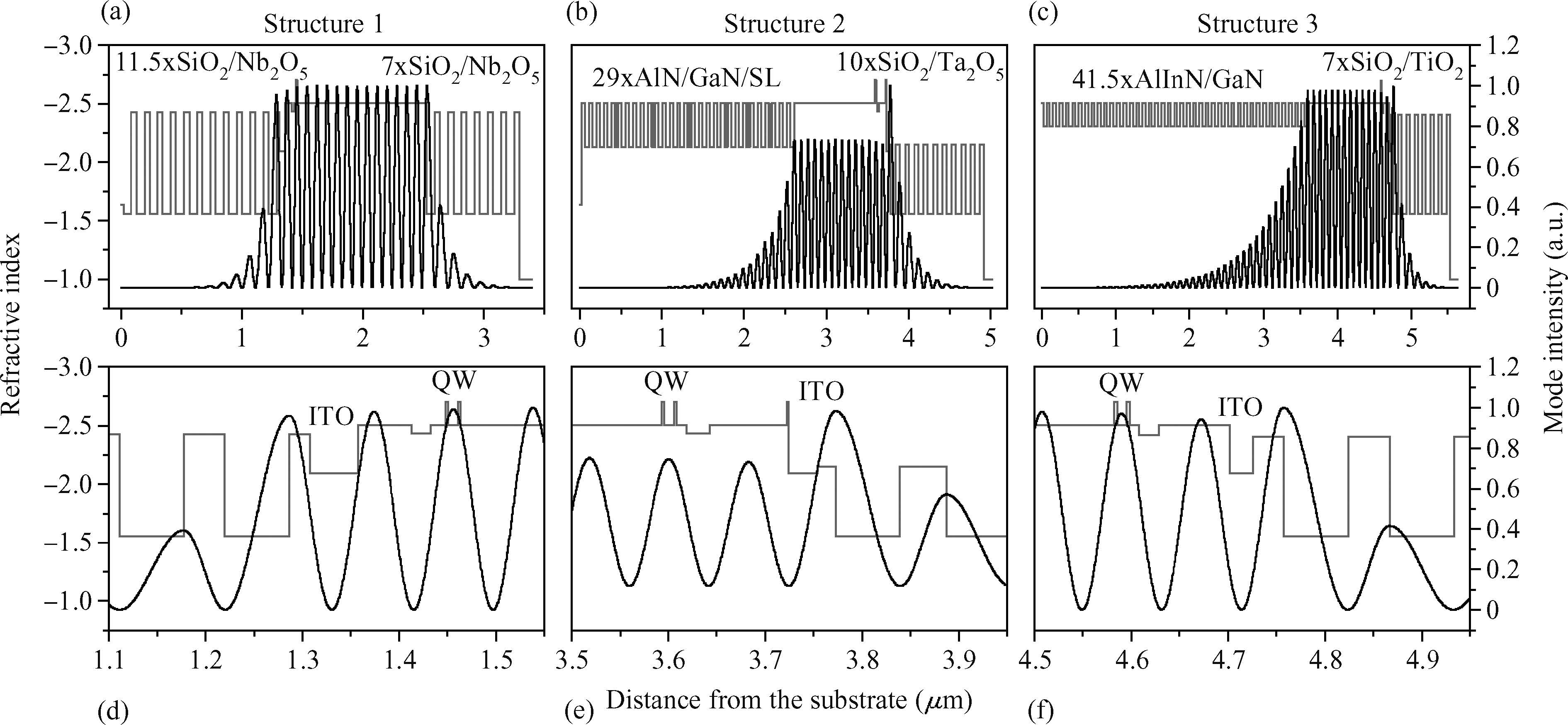
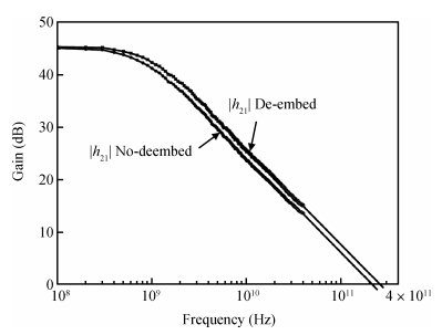
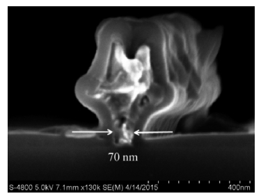
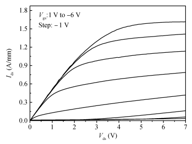
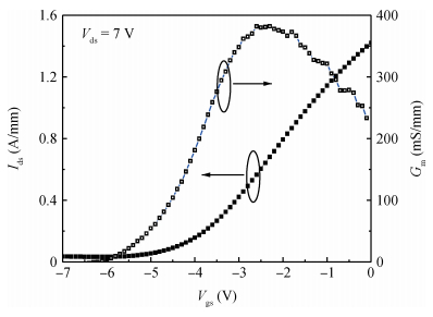
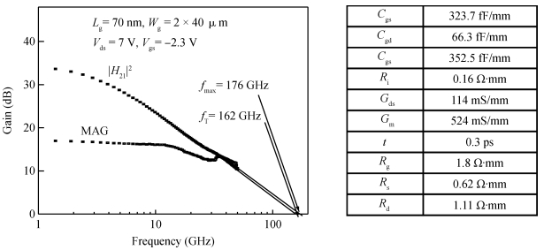
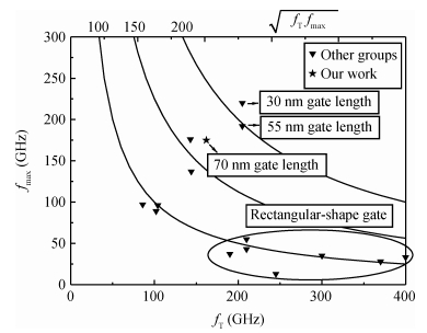
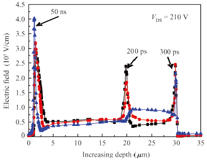
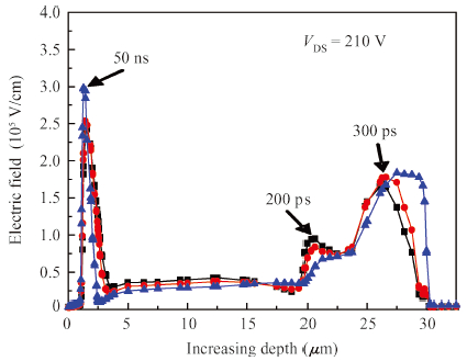
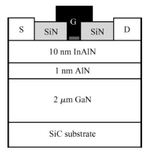
InAlN/GaN high-electron-mobility transistors (HEMTs) on SiC substrate were fabricated and characterized. Several techniques, consisting of high electron density, 70 nm T-shaped gate, low ohmic contacts and a short drain-source distance, are integrated to gain high device performance. The fabricated InAlN/GaN HEMTs exhibit a maximum drain saturation current density of 1.65 A/mm at Vgs = 1 V and a maximum peak transconductance of 382 mS/mm. In addition, a unity current gain cut-off frequency (fT) of 162 GHz and a maximum oscillation frequency (fmax) of 176 GHz are achieved on the devices with the 70 nm gate length.

J. Semicond.
2016, 37(2): 024008 doi: 10.1088/1674-4926/37/2/024008

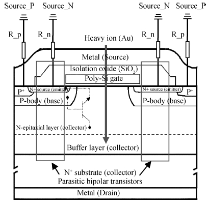
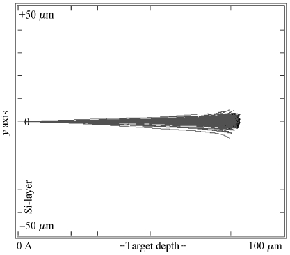
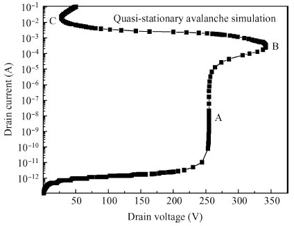
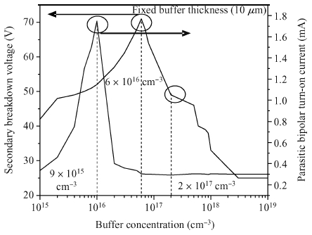
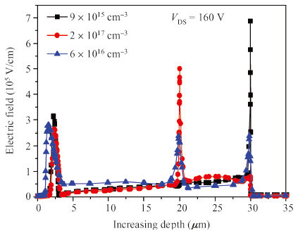
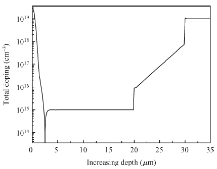
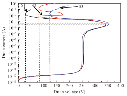
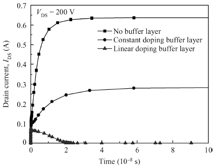
The addition of a buffer layer can improve the device's secondary breakdown voltage, thus, improving the single event burnout (SEB) threshold voltage. In this paper, an N type linear doping buffer layer is proposed. According to quasi-stationary avalanche simulation and heavy ion beam simulation, the results show that an optimized linear doping buffer layer is critical. As SEB is induced by heavy ions impacting, the electric field of an optimized linear doping buffer device is much lower than that with an optimized constant doping buffer layer at a given buffer layer thickness and the same biasing voltages. Secondary breakdown voltage and the parasitic bipolar turn-on current are much higher than those with the optimized constant doping buffer layer. So the linear buffer layer is more advantageous to improving the device's SEB performance.
J. Semicond.
2016, 37(2): 024009 doi: 10.1088/1674-4926/37/2/024009
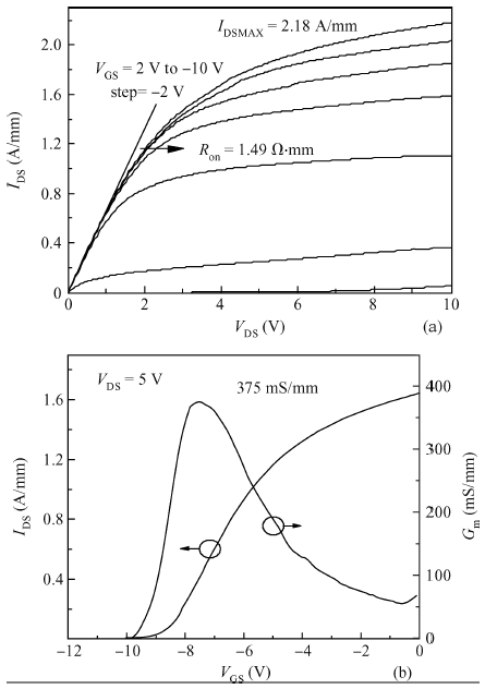
InAlN/GaN high-electron mobility transistors (HEMTs) with a gate length of 100 nm and oxygen plasma treatment were fabricated. A Si/Ti/Al/Ni/Au ohmic contact was also used to reduce the contact resistance. DC and RF characteristics of the devices were measured. The fabricated devices show a maximum drain current density of 2.18 A/mm at VGS = 2 V, a low on-resistance (Ron) of 1.49 Ω·mm and low gate leakage current. An excellent frequency response was also obtained. The current cut-off frequency (fT) is 81 GHz and the maximum oscillation frequency is 138 GHz, respectively.


J. Semicond.
2016, 37(2): 024010 doi: 10.1088/1674-4926/37/2/024010
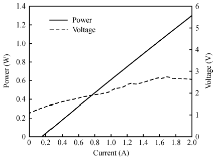
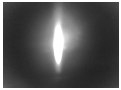
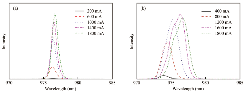
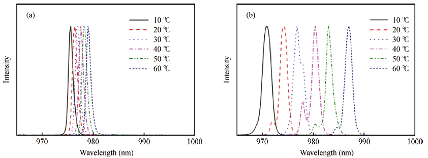
To achieve high pumping efficiency and stability, a wavelength stabilized 980 nm broad area distributed feedback laser was realized. A nanoimprint lithography technique was used to fabricate the first-order gratings. The stripe width was 90 μm and the cavity length was 2 mm. Under continuous wave condition, the output laser power reached 1.2 W, with the slope efficiency of 0.7 W/A. The current and thermal dependence of the spectrum peak was measured to be approximately 0.19 nm/A and 0.064 nm/K respectively, and the wavelength-locking range reached over 50 ℃.

J. Semicond.
2016, 37(2): 024011 doi: 10.1088/1674-4926/37/2/024011
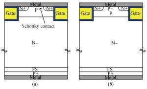
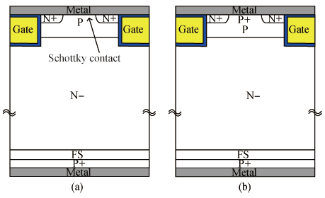
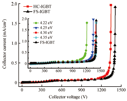
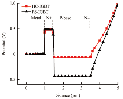
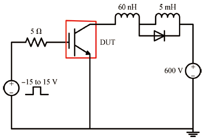
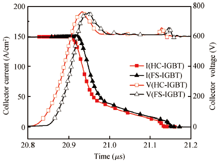
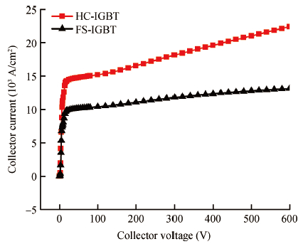
This letter proposes a high-conductivity insulated gate bipolar transistor (HC-IGBT) with Schottky contact formed on the p-base, which forms a hole barrier at the p-base side to enhance the conductivity modulation effect. TCAD simulation shows that the HC-IGBT provides a current density increase by 53% and turn-off losses decrease by 27% when compared to a conventional field-stop IGBT (FS-IGBT). Hence, the proposed IGBT exhibits superior electrical performance for high-efficiency power electronic systems.


J. Semicond.
2016, 37(2): 025001 doi: 10.1088/1674-4926/37/2/025001
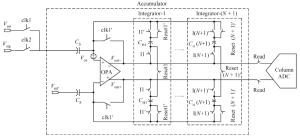
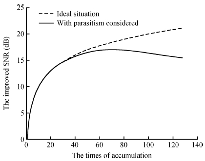
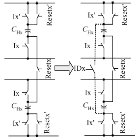
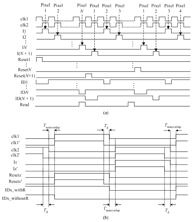
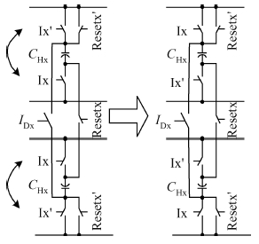
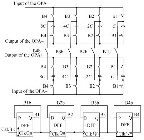
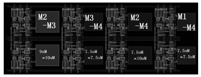
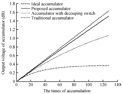
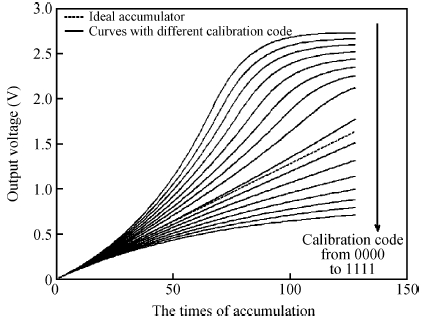
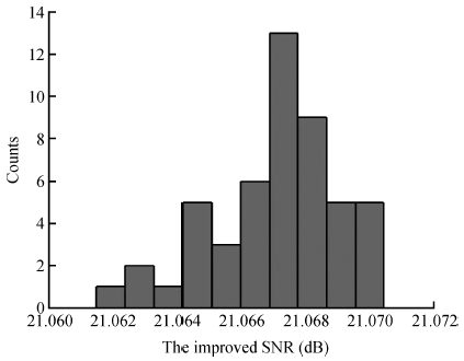
The impact of the parasitic phenomenon on the performance of the analog accumulator in TDI CMOS image sensor is analyzed and resolved. A 128-stage optimized accumulator based on 0.18-μ m one-poly four-metal 3.3 V CMOS technology is designed and simulated. A charge injection effect from the top plate sampling is employed to compensate the un-eliminated parasitics based on the accumulator with a decoupling switch, and then a calibration circuit is designed to restrain the mismatch and Process, Voltage and Temperature (PVT) variations. The post layout simulation indicates that the improved SNR of the accumulator upgrades from 17.835 to 21.067 dB, while an ideal value is 21.072 dB. In addition, the linearity of the accumulator is 99.62%. The simulation results of two extreme cases and Monte Carlo show that the mismatch and PVT variations are restrained by the calibration circuit. Furthermore, it is promising to design a higher stage accumulator based on the proposed structure.


J. Semicond.
2016, 37(2): 025002 doi: 10.1088/1674-4926/37/2/025002
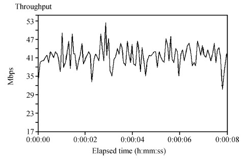
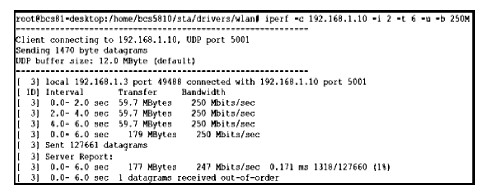
An IEEE-802.11ac-1*1 wireless LAN system-on-a-chip (SoC) that integrates an analog front end, a digital base-band processor and a media access controller has been implemented in 65 nm CMOS technology. It can provide significantly increased throughput, high efficiency rate selection, and fully backward compatibility with the existing 802.11a/n WLAN protocols. Especially the measured maximum throughput of UDP traffic can be up to 267 Mbps.
J. Semicond.
2016, 37(2): 025003 doi: 10.1088/1674-4926/37/2/025003

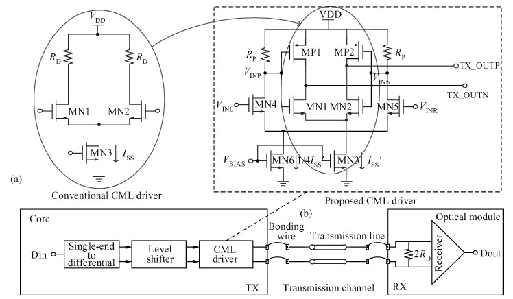
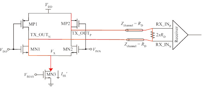
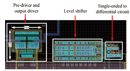
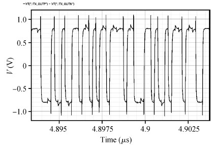
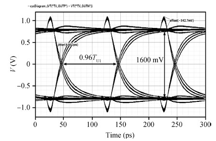
High static power limits the application of conventional current-mode logic (CML). This paper presents a power-efficient switchable CML driver, which achieves a significant current saving by 75% compared with conventional ones. Implemented in the 130 nm CMOS technology process, the proposed CML driver just occupies an area about 0.003 mm2 and provides a robust differential signal of 1600 mV for 10 Gbps optical line terminal (OLT) with a total current of 10 mA. The peak-to-peak jitter is about 4 ps (0.04TUI) and the offset voltage is 347.2 mV @ 1600 mVPP.
J. Semicond.
2016, 37(2): 025004 doi: 10.1088/1674-4926/37/2/025004
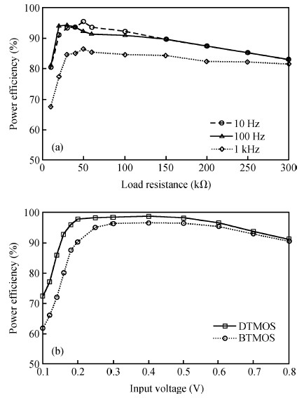
An ultra low voltage rectifier with high power conversion efficiency (PCE) for PE energy harvesting applications is presented in this paper. This is achieved by utilizing the DTMOS which the body terminal is connected to the gate terminal in a diode connected transistor. This implementation facilitates the rectifier with dynamic control over the threshold voltage. Moreover, we use input powered to take the place of output powered to reduce the power loss and thereby increasing the power conversion efficiency. Based on standard SMIC 0.18 μm CMOS technology, the simulation results show that the voltage conversion efficiency and the power conversion efficiency can reach up to 90.5% and 95.5% respectively, when the input voltage equals to 0.2 V @ 100 Hz with load resistance 50 kΩ . Input voltages with frequencies in the range of 10 Hz-1 kHz can be rectified.

J. Semicond.
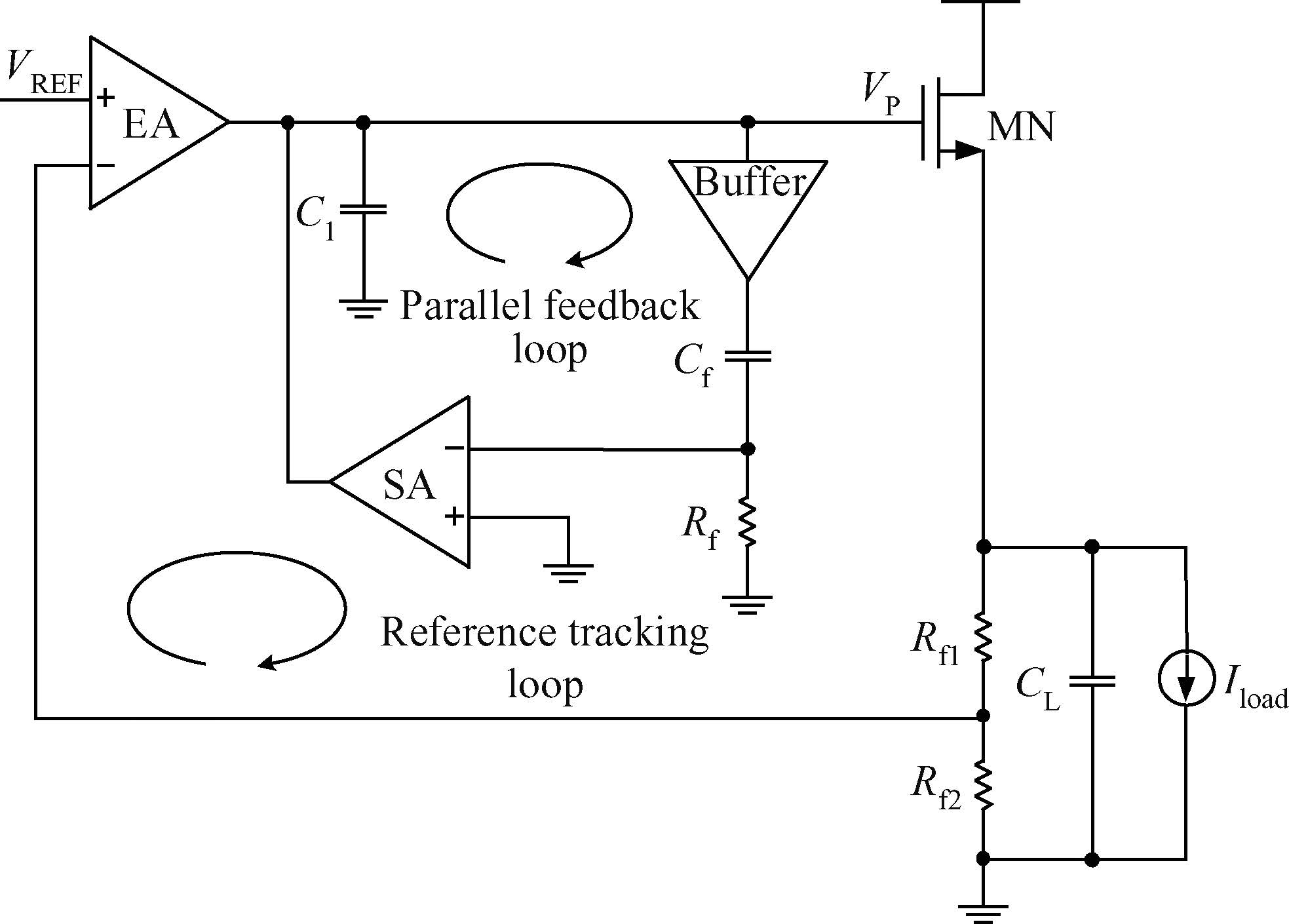
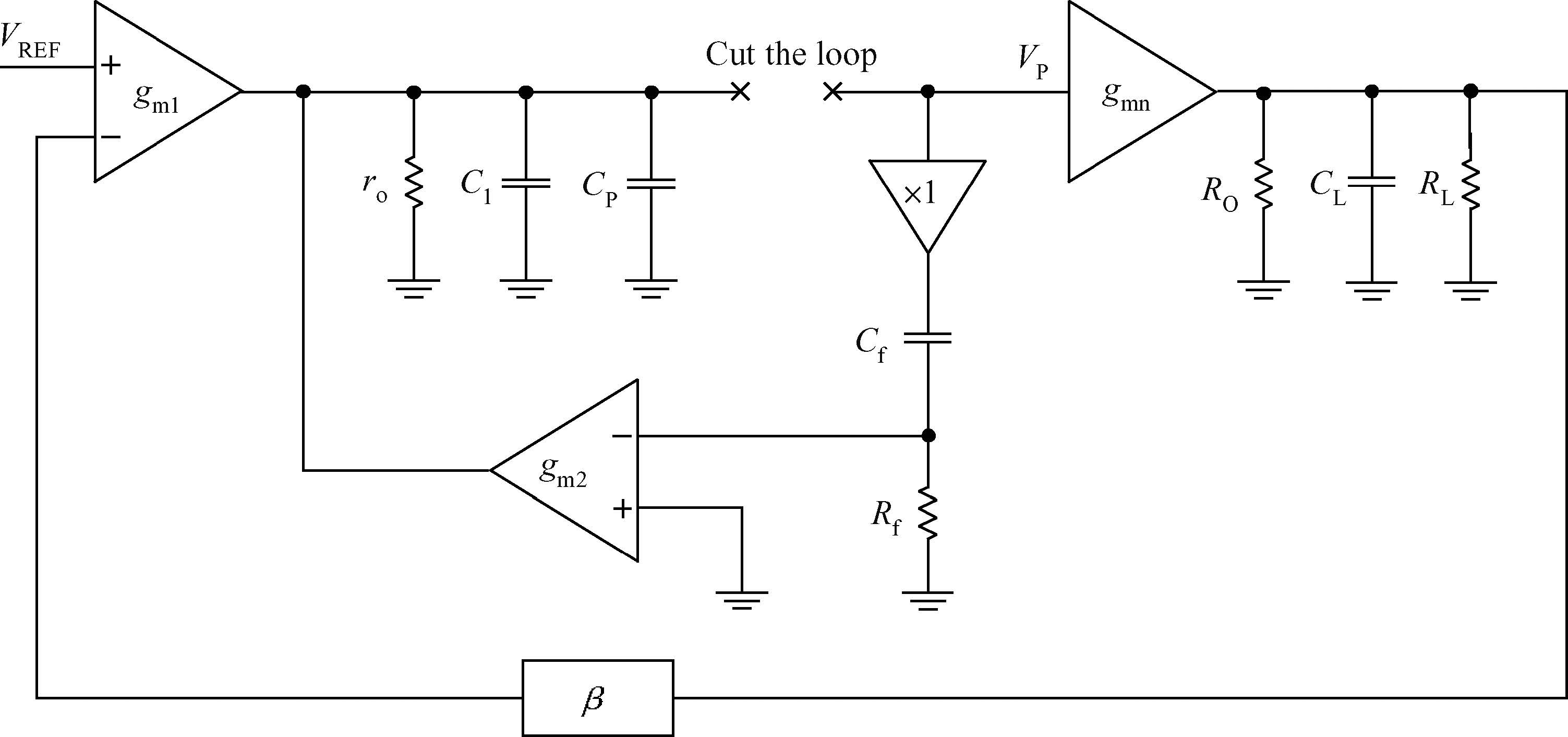
2016, 37(2): 025005 doi: 10.1088/1674-4926/37/2/025005
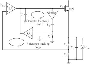
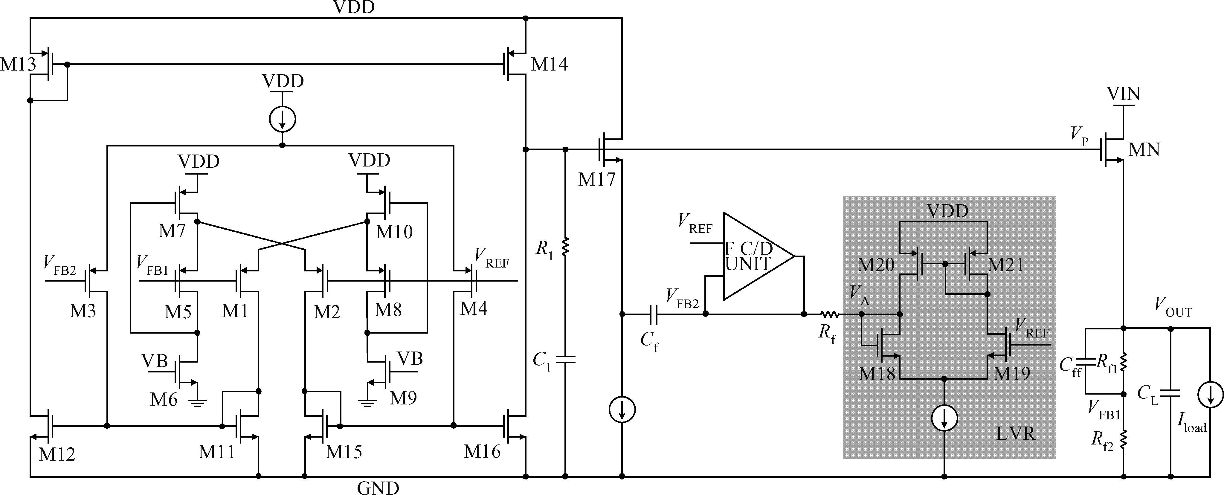
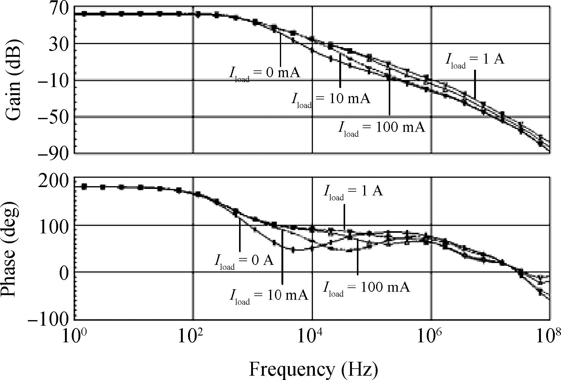
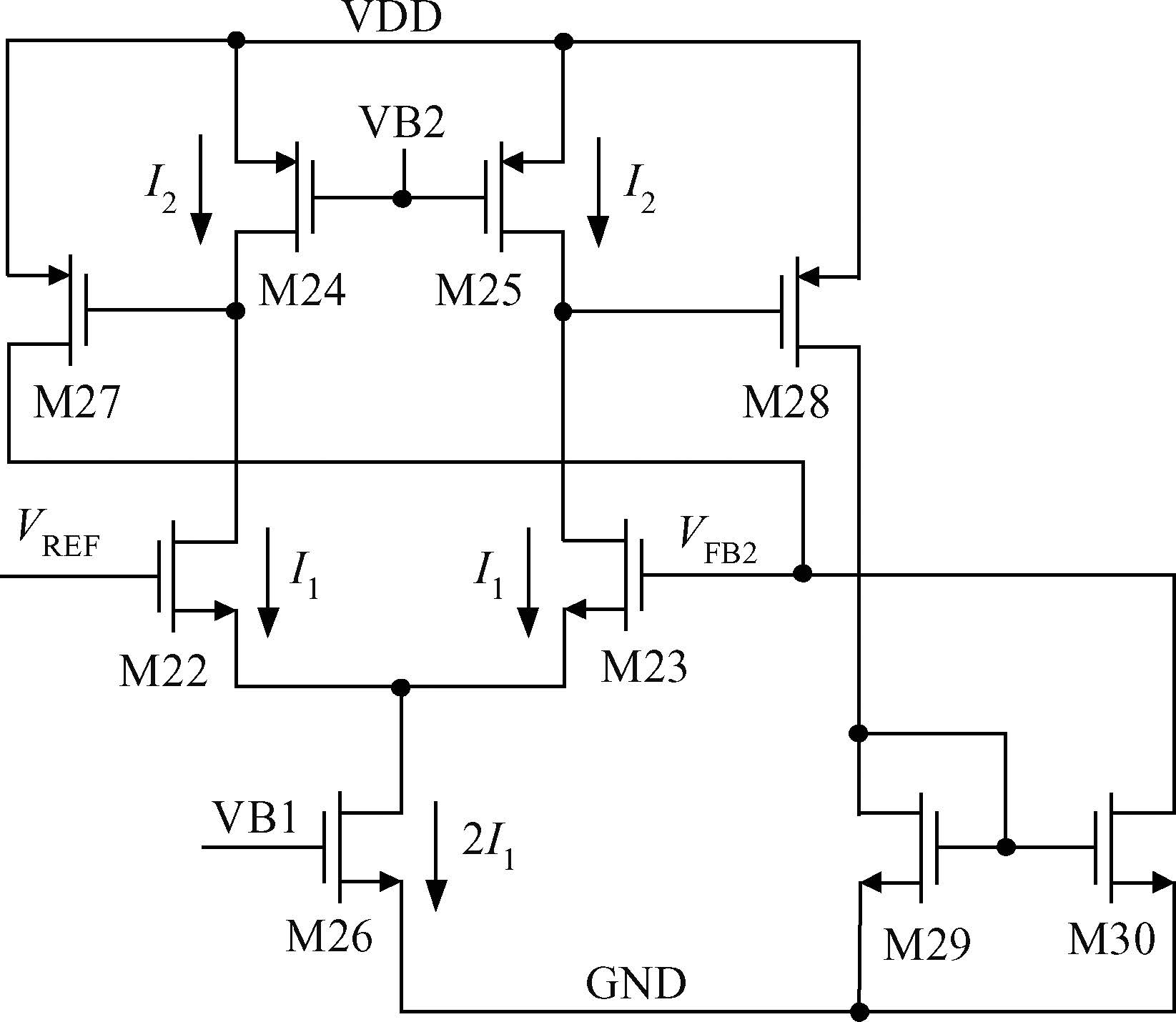
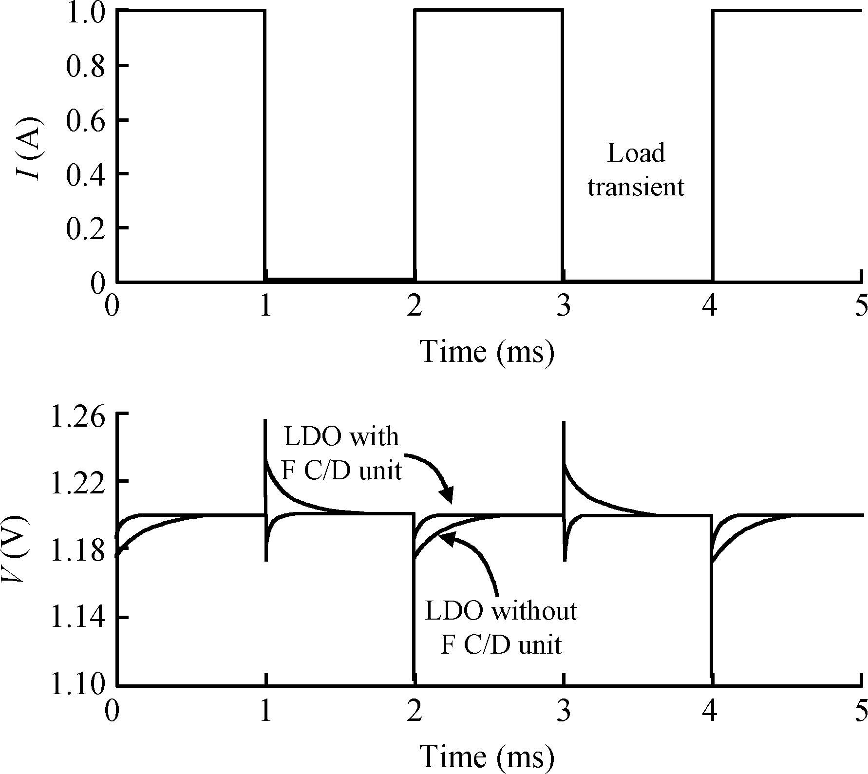
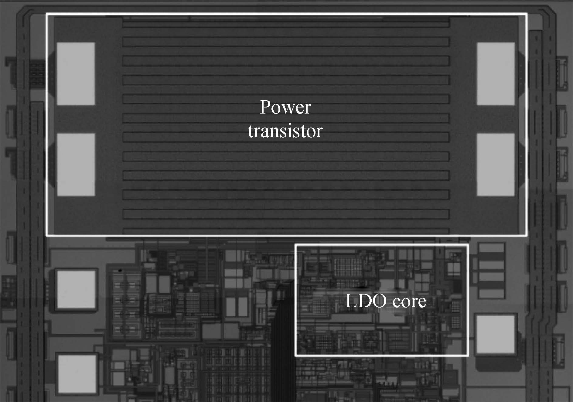
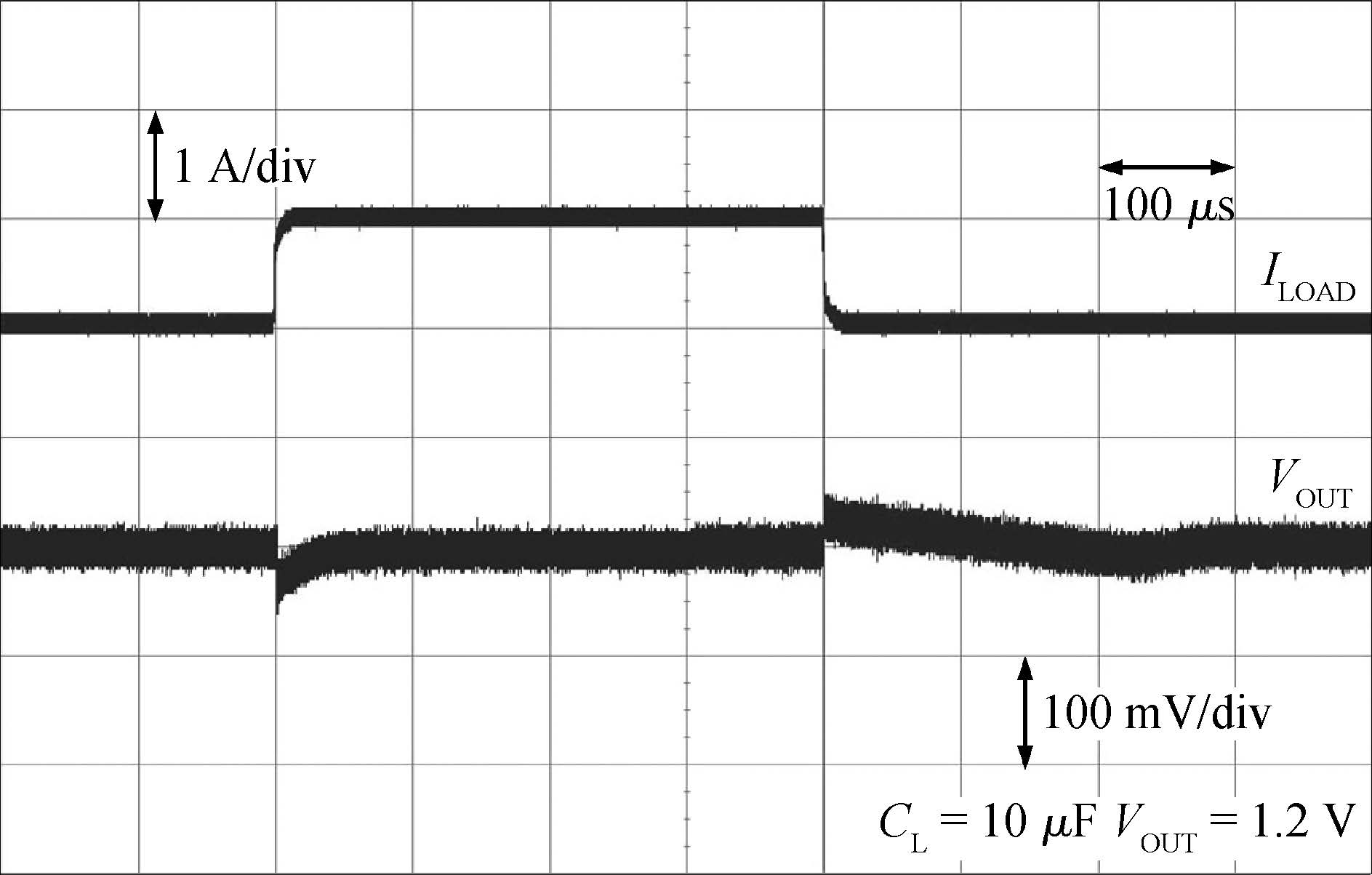
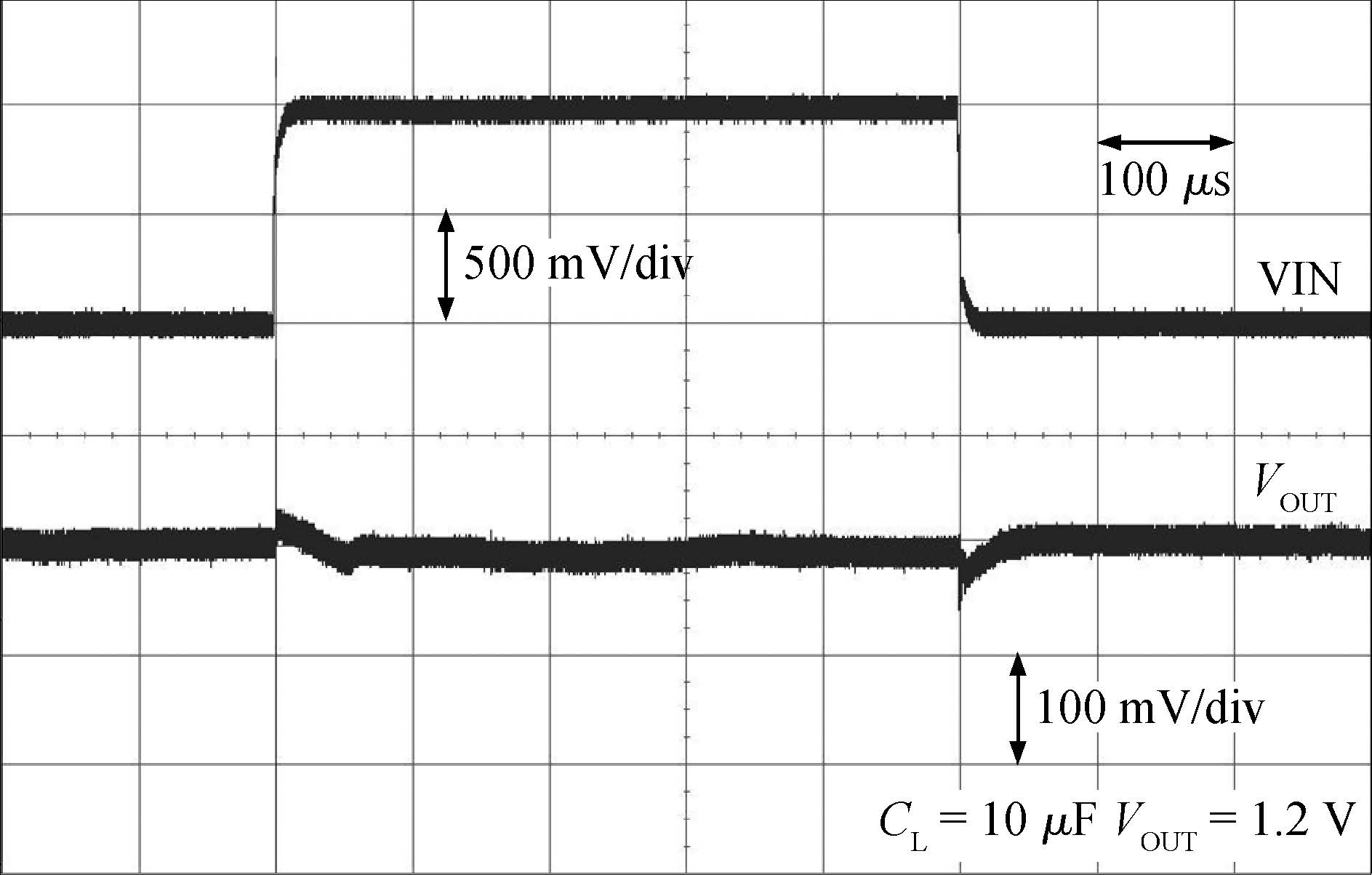
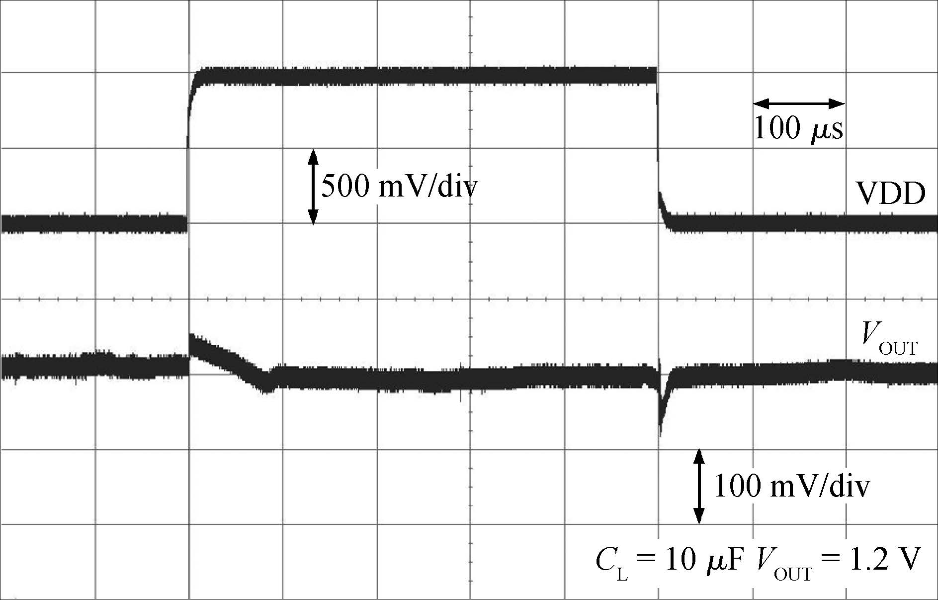
This paper presents a transient-enhanced NMOS low-dropout regulator (LDO) for portable applications with parallel feedback compensation. The parallel feedback structure adds a dynamic zero to get an adequate phase margin with a load current variation from 0 to 1 A. A class-AB error amplifier and a fast charging/discharging unit are adopted to enhance the transient performance. The proposed LDO has been implemented in a 0.35 μ m BCD process. From experimental results, the regulator can operate with a minimum dropout voltage of 150 mV at a maximum 1 A load and IQ of 165 μ A. Under the full range load current step, the voltage undershoot and overshoot of the proposed LDO are reduced to 38 mV and 27 mV respectively.
J. Semicond.
2016, 37(2): 025006 doi: 10.1088/1674-4926/37/2/025006

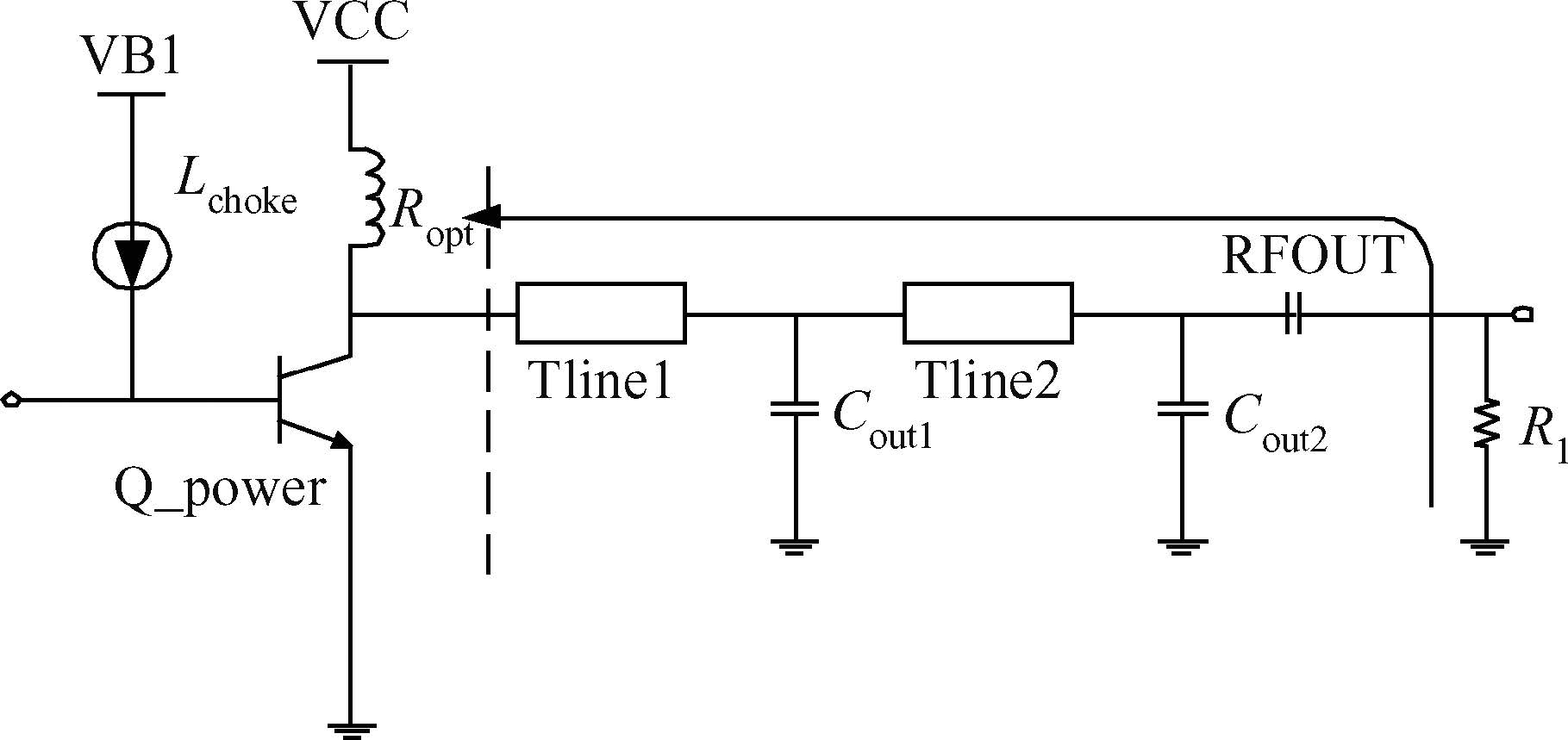
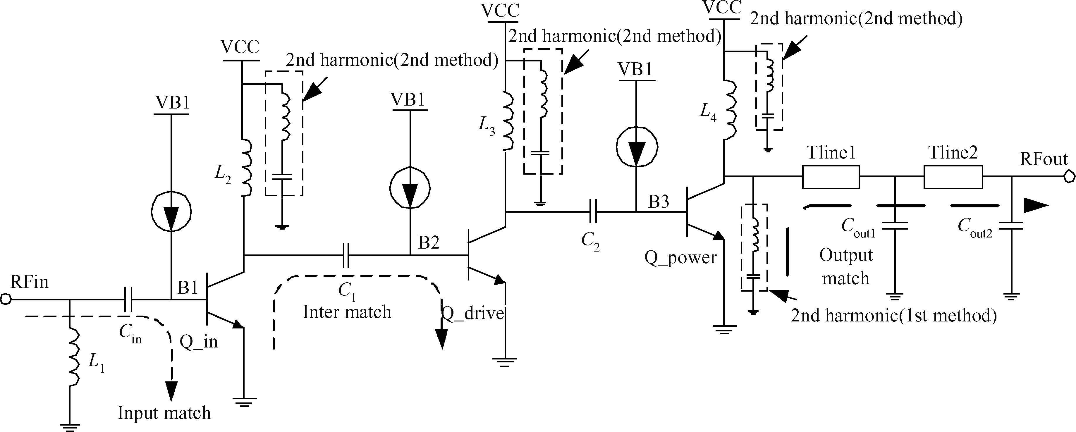
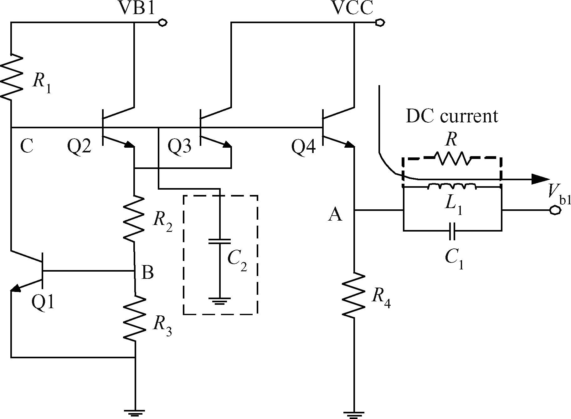
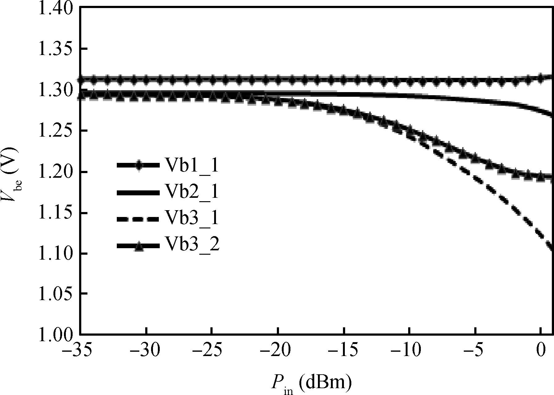
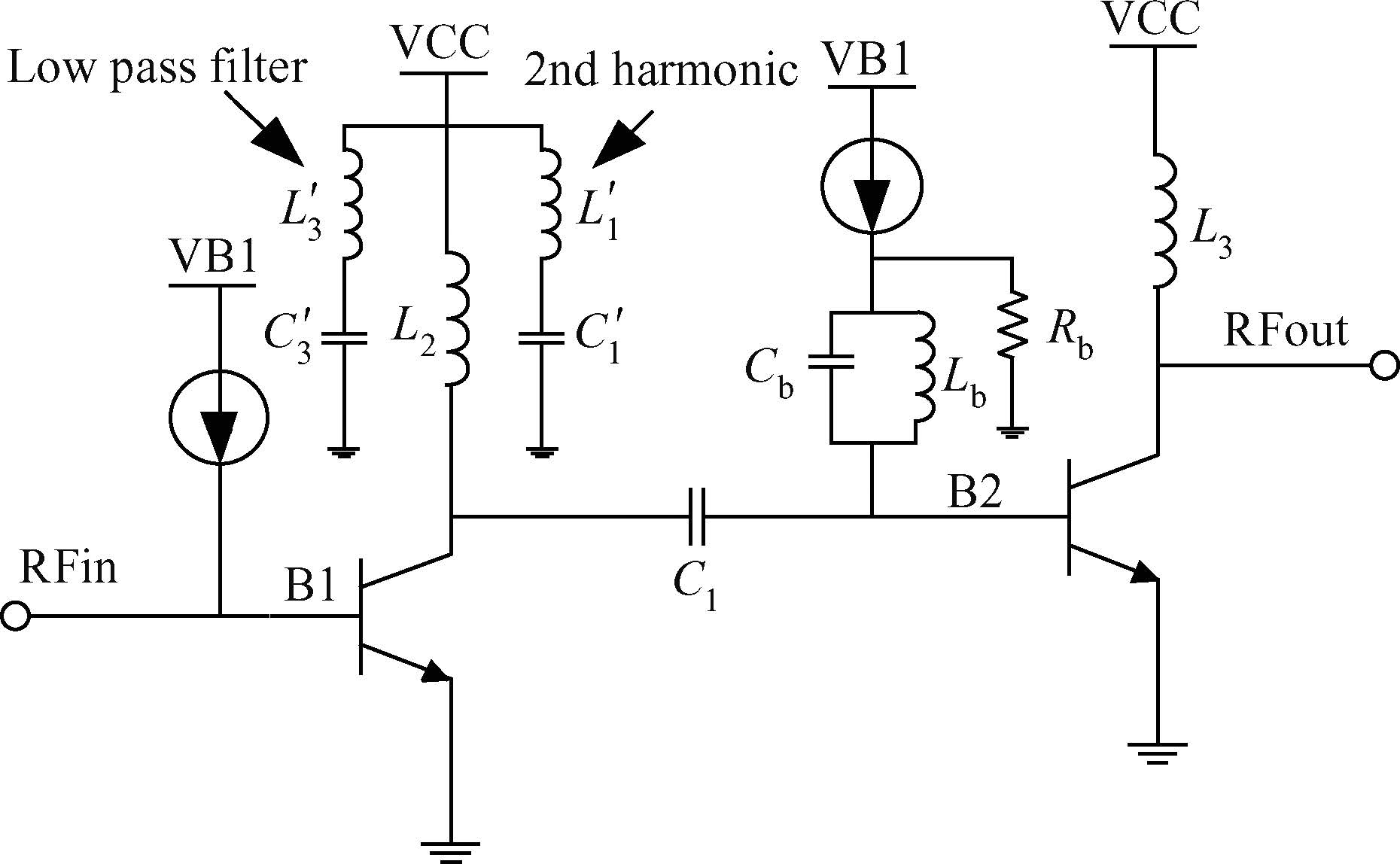
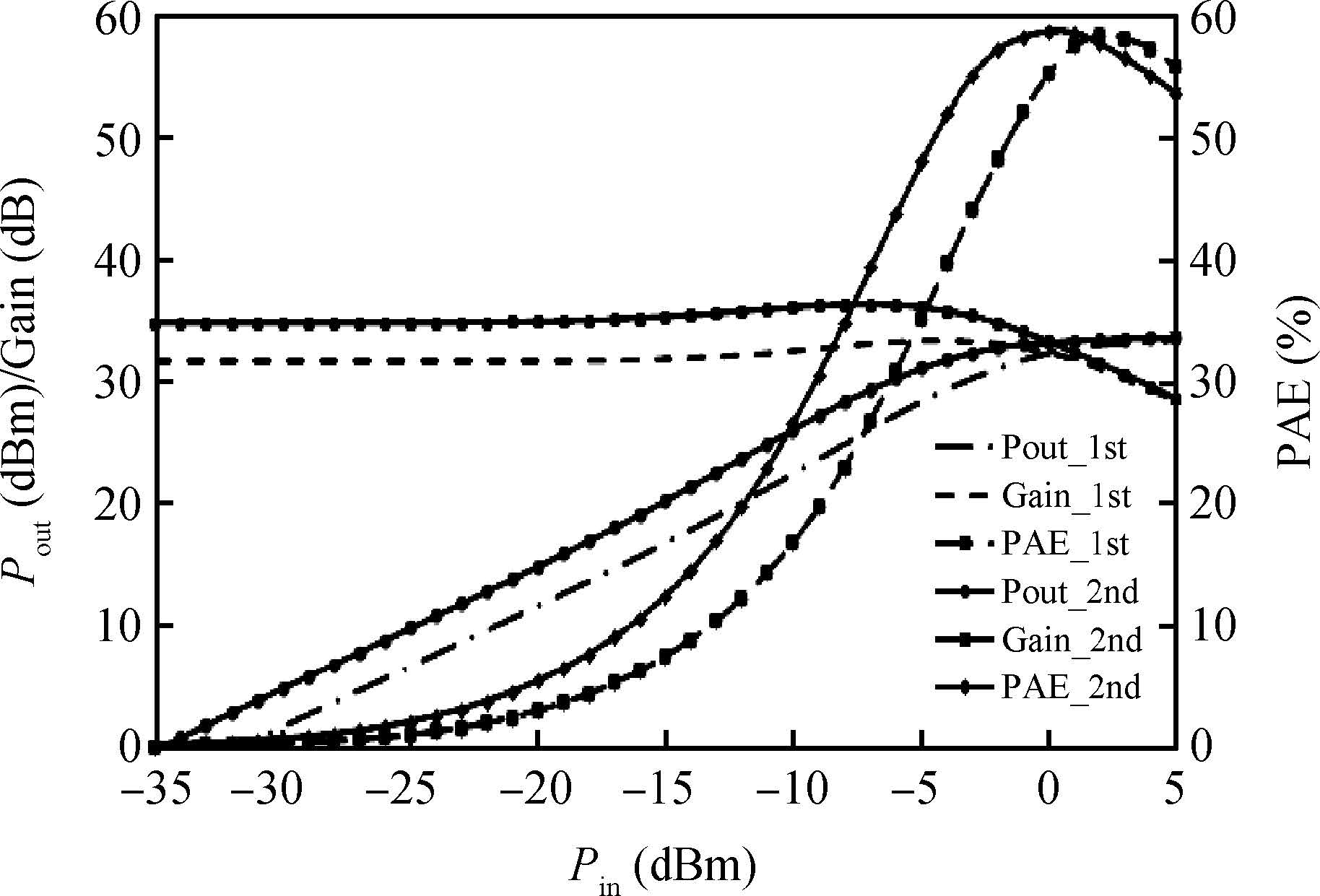
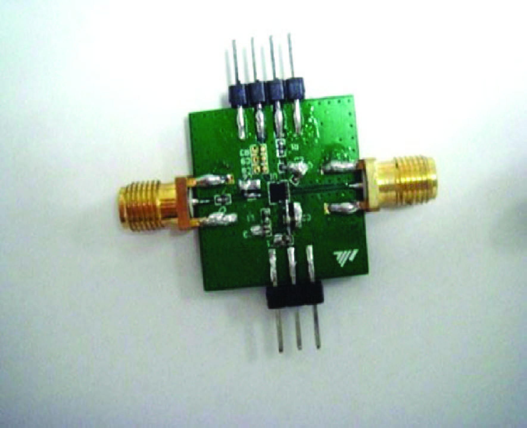
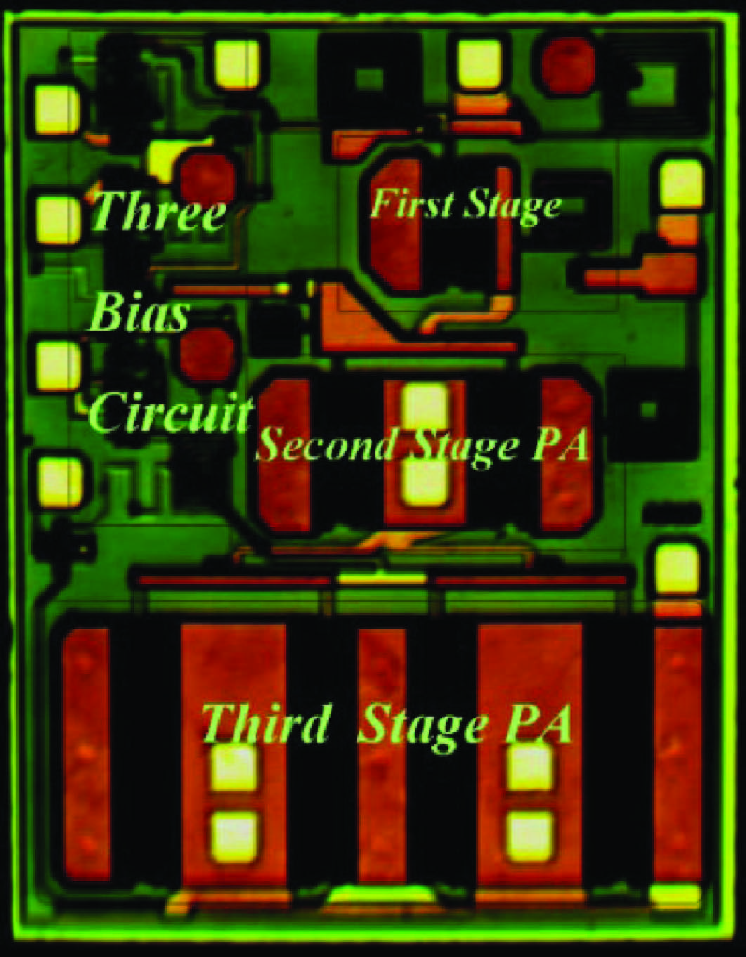
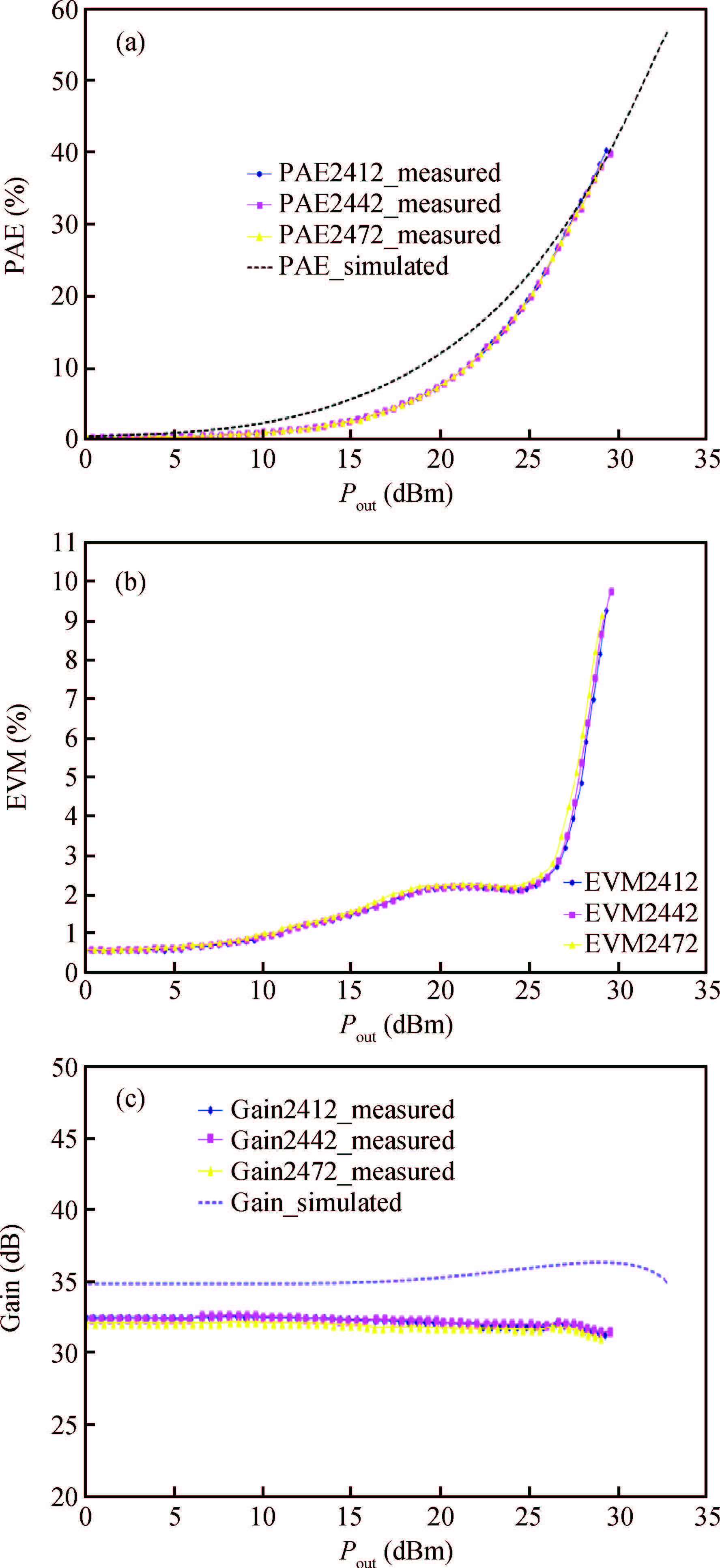
A three-stage power amplifier (PA) for WLAN application in 2.4-2.5 GHz is presented. The proposed PA employs an adaptive bias circuit to adjust the operating point of the PA to improve the linearity of the PA. Two methods to short the 2nd harmonic circuit are compared in the area of efficiency and gain of the PA. The PA is taped out in the process of 2 μm InGaP/GaAs HBT and is tested by the evaluation board. The measured results show that 31.5 dB power gain and 29.3 dBm P1dB with an associated 40.4% power added efficiency (PAE) under the single tone stimulus. Up to 26.5 dBm output power can be achieved with an error vector magnitude (EVM) of lower than 3% under the 64QAM/OFDM WLAN stimulus.

J. Semicond.
2016, 37(2): 025007 doi: 10.1088/1674-4926/37/2/025007
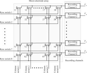
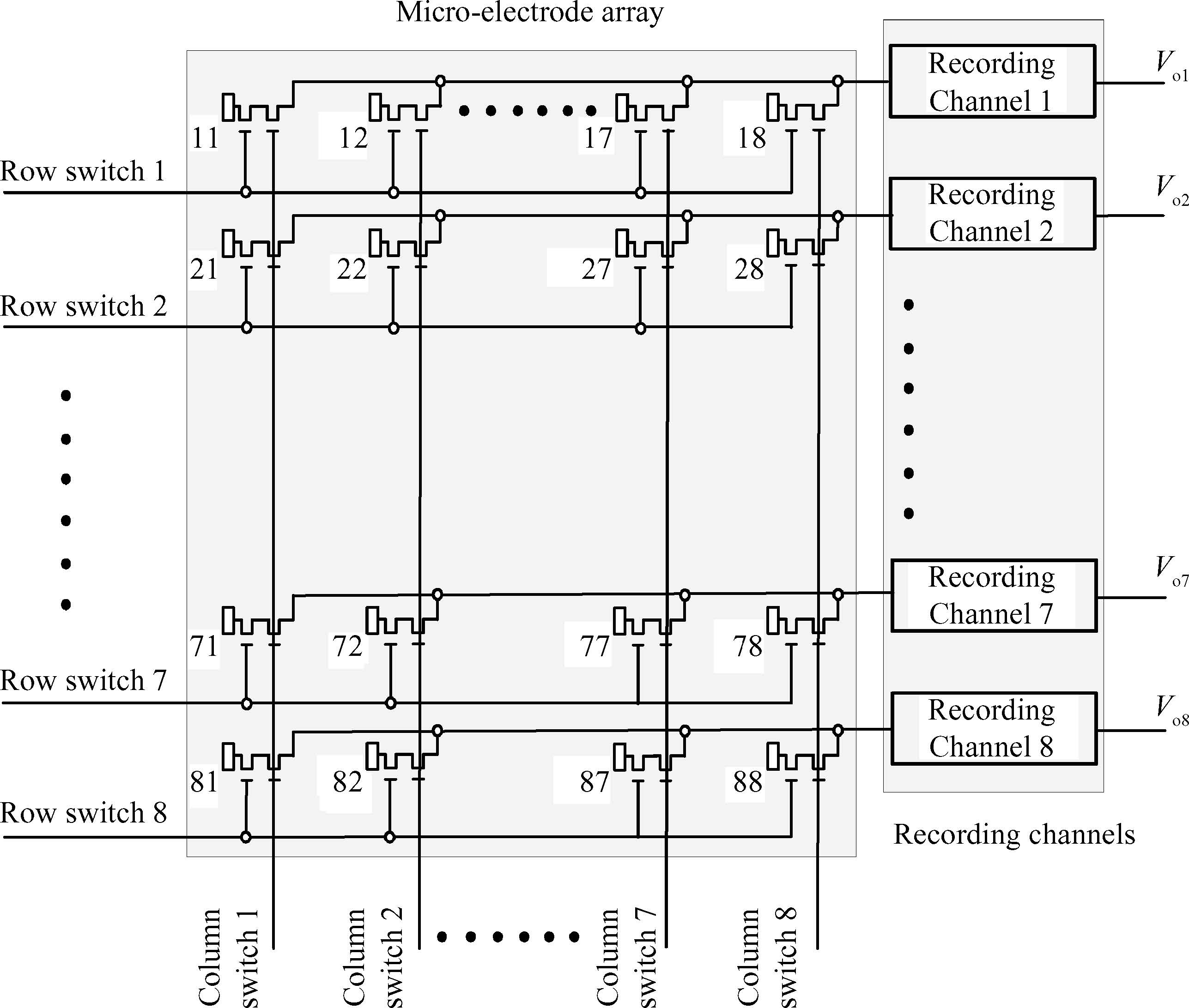
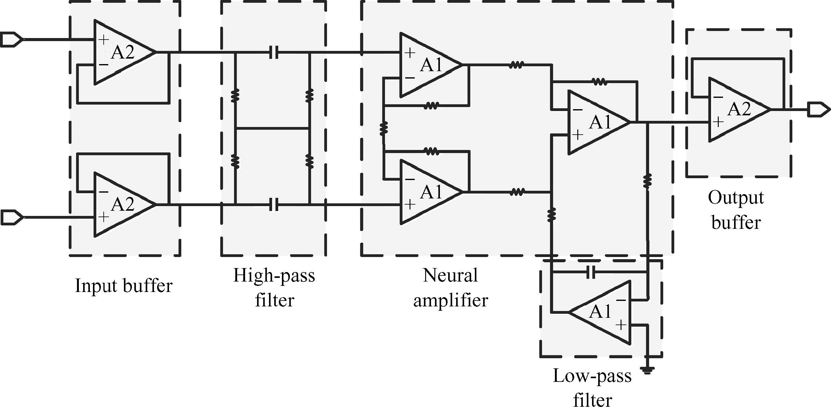
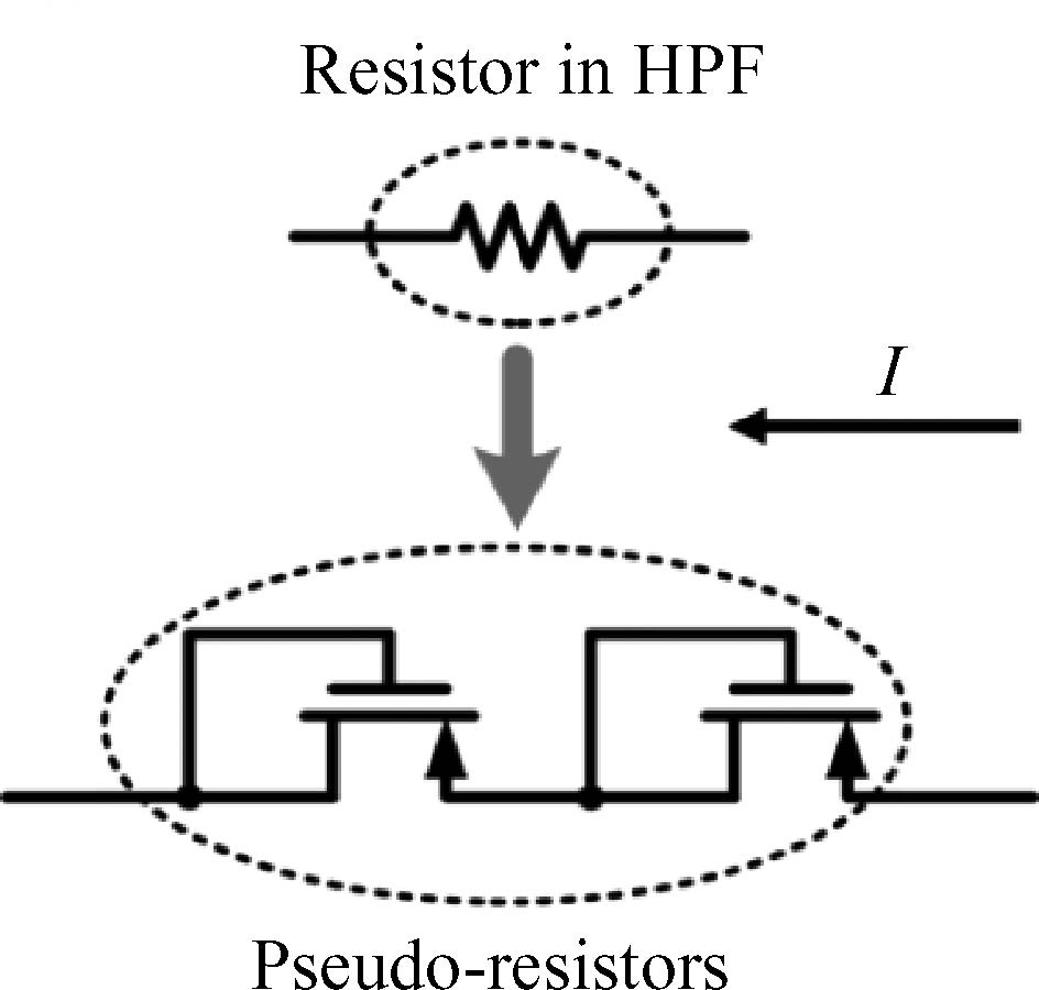
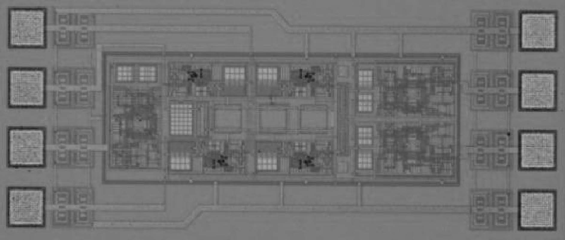
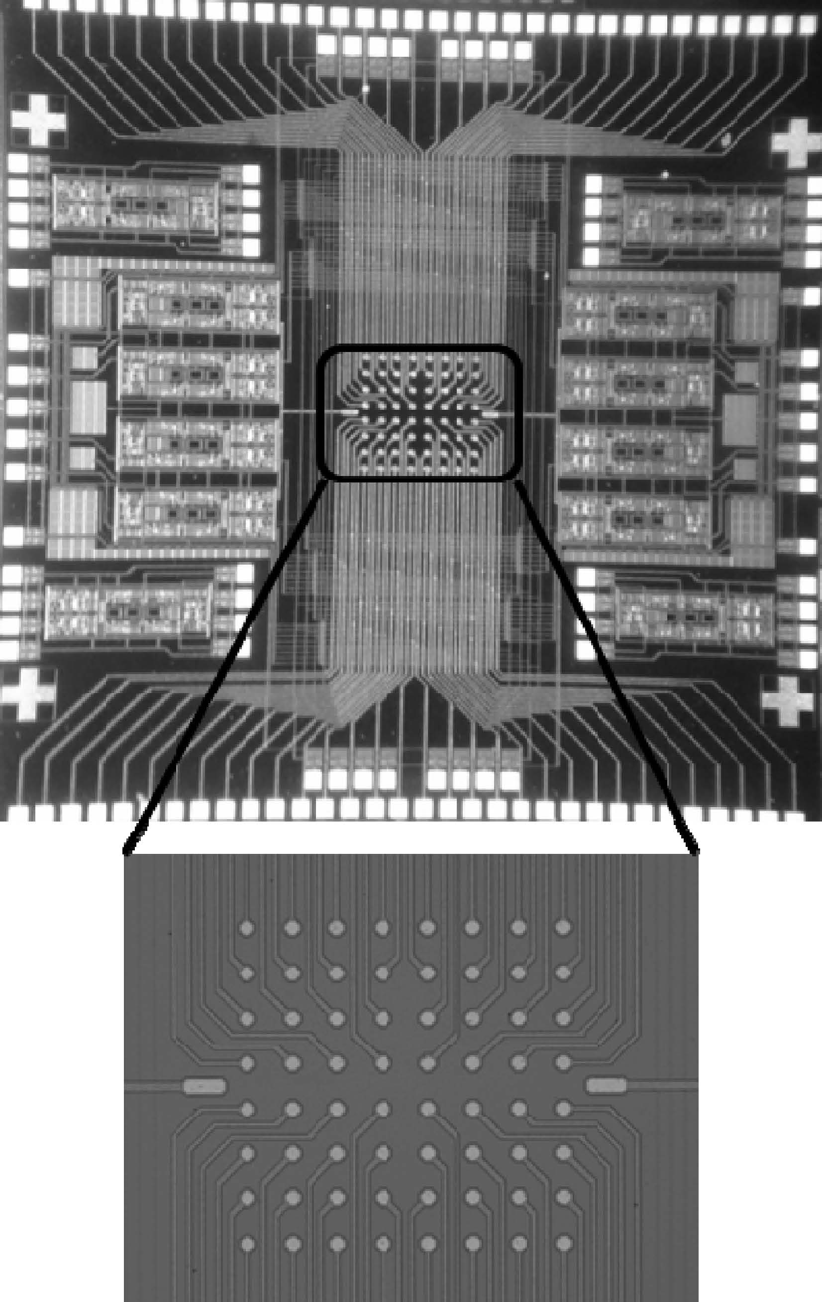
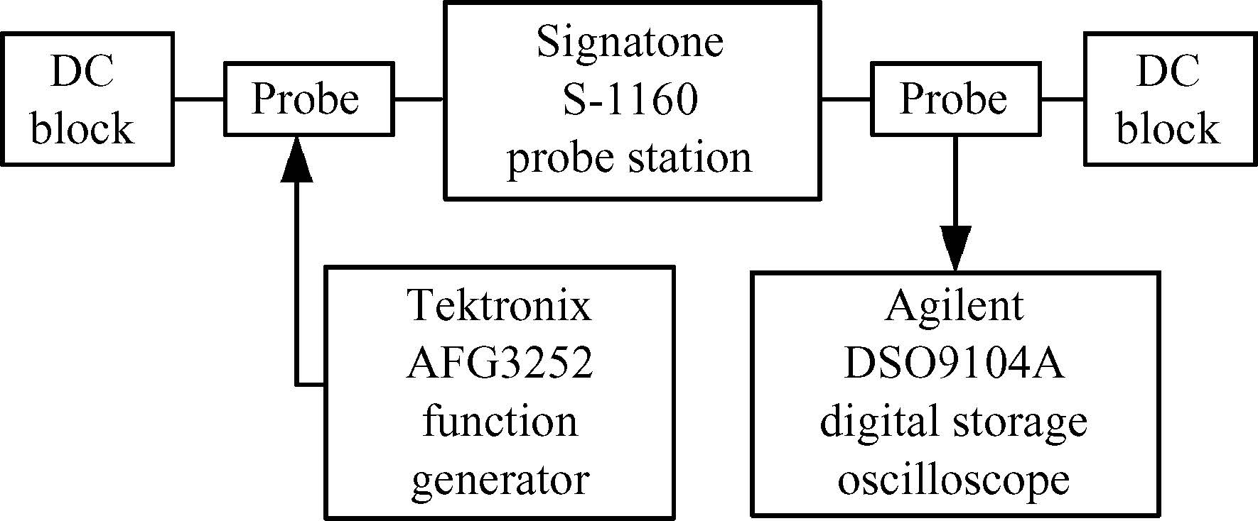
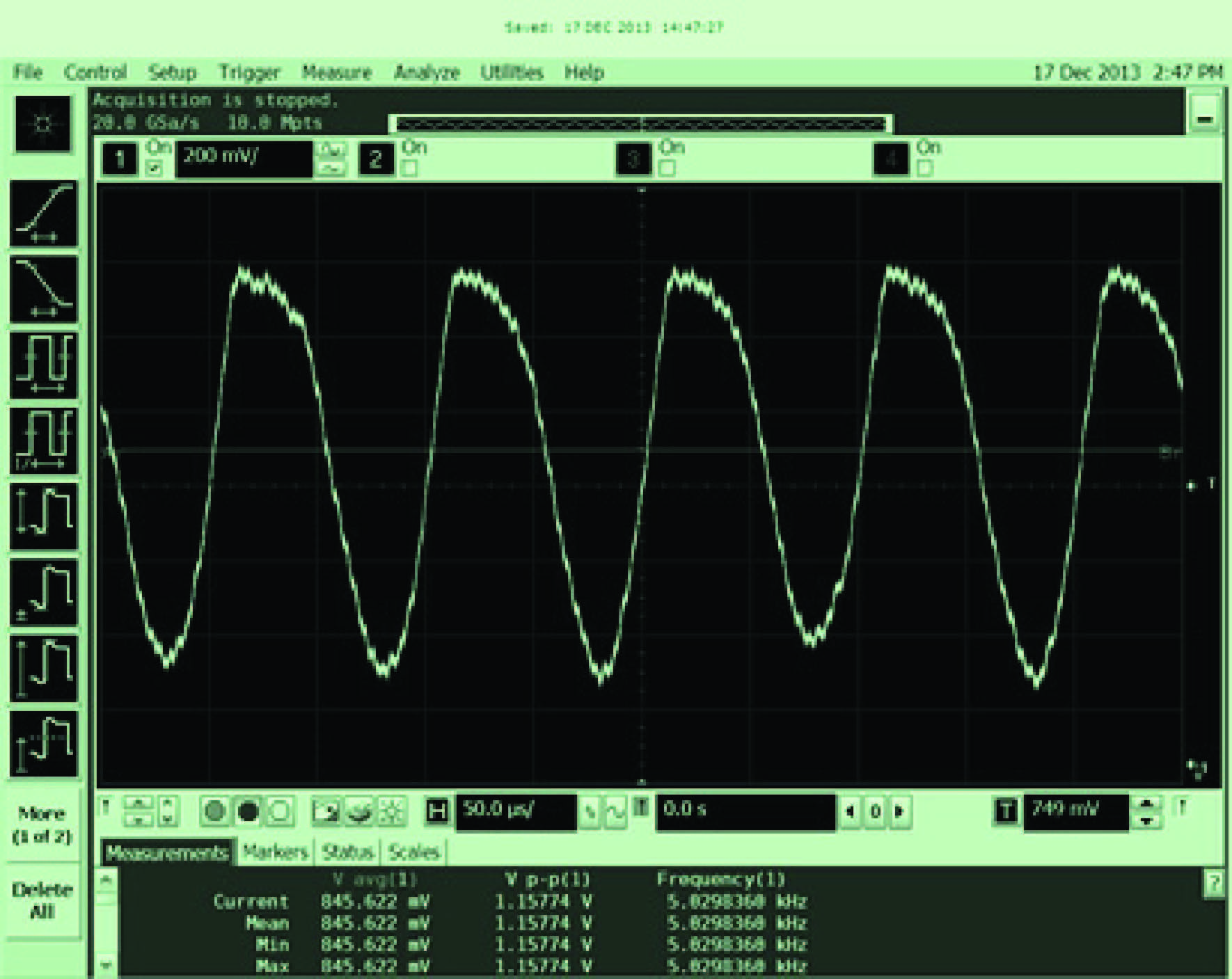
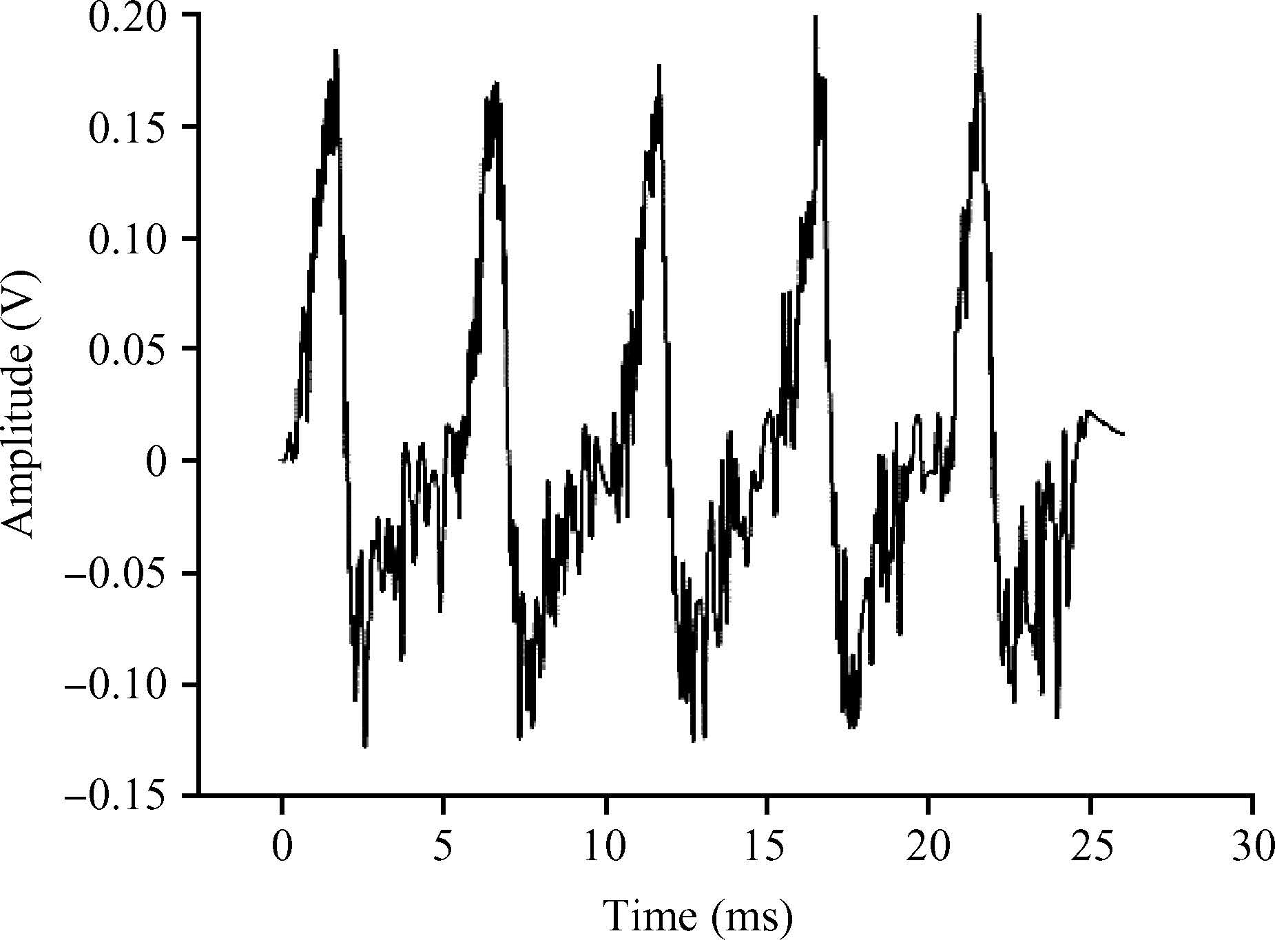
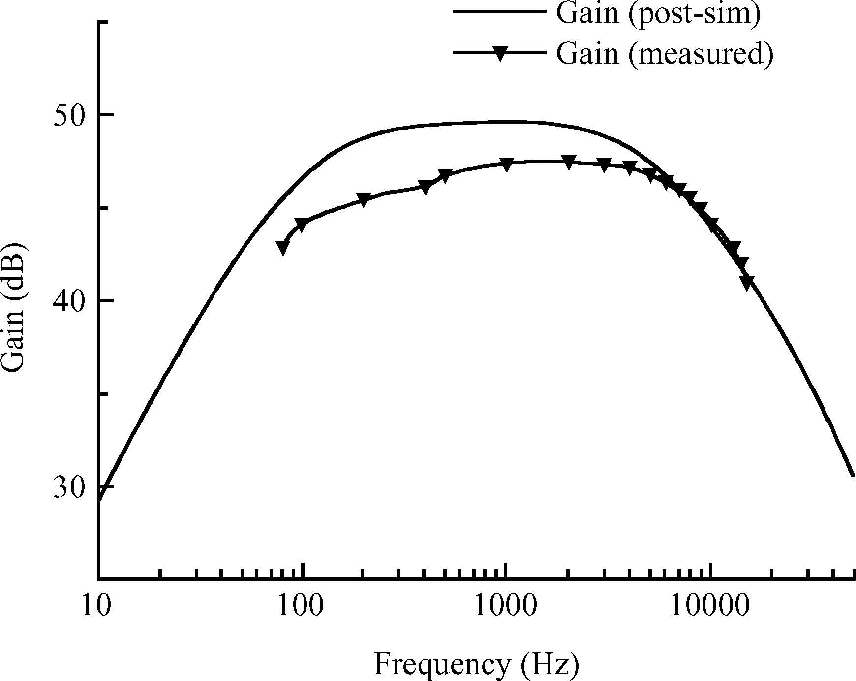
Recent work in the field of neurophysiology has demonstrated that, by observing the firing characteristic of action potentials (AP) and the exchange pattern of signals between neurons, it is possible to reveal the nature of "memory" and "thinking" and help humans to understand how the brain works. To address these needs, we developed a prototype fully integrated circuit (IC) with micro-electrode array (MEA) for neural recording. In this scheme, the microelectrode array is composed by 64 detection electrodes and 2 reference electrodes. The proposed IC consists of 8 recording channels with an area of 5 × 5 mm2. Each channel can operate independently to process the neural signal by amplifying, filtering, etc. The chip is fabricated in 0.5-μ m CMOS technology. The simulated and measured results show the system provides an effective device for recording feeble signal such as neural signals.
J. Semicond.
2016, 37(2): 026001 doi: 10.1088/1674-4926/37/2/026001

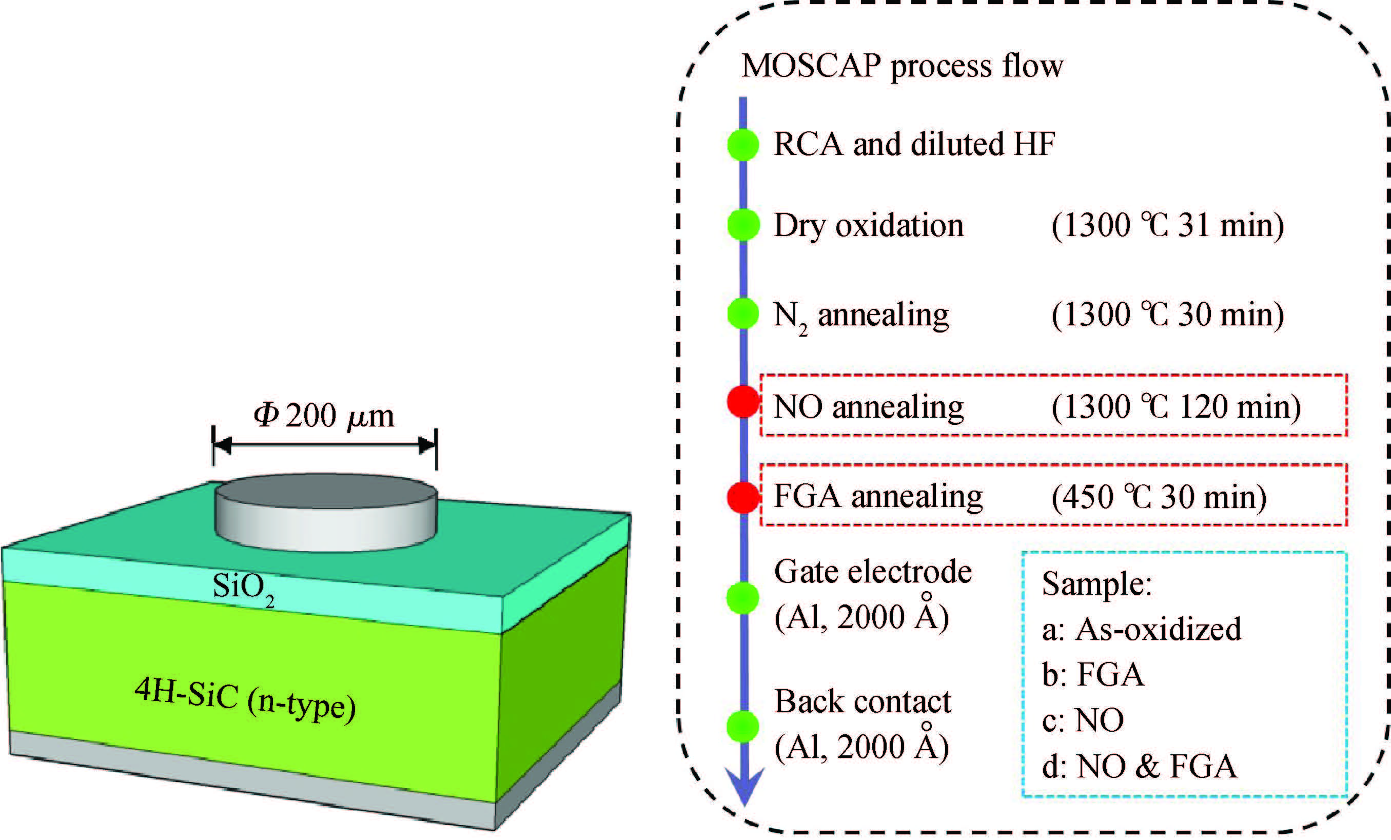
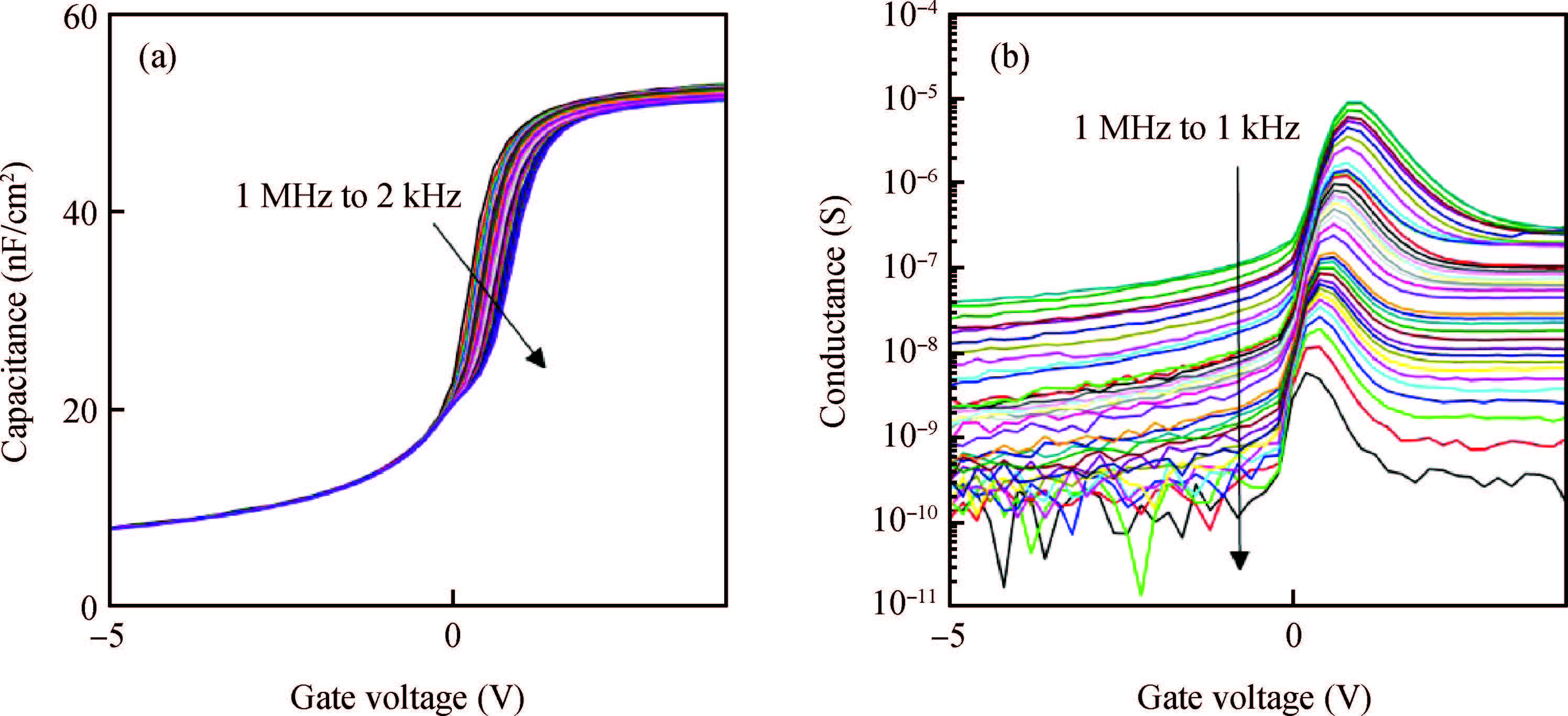
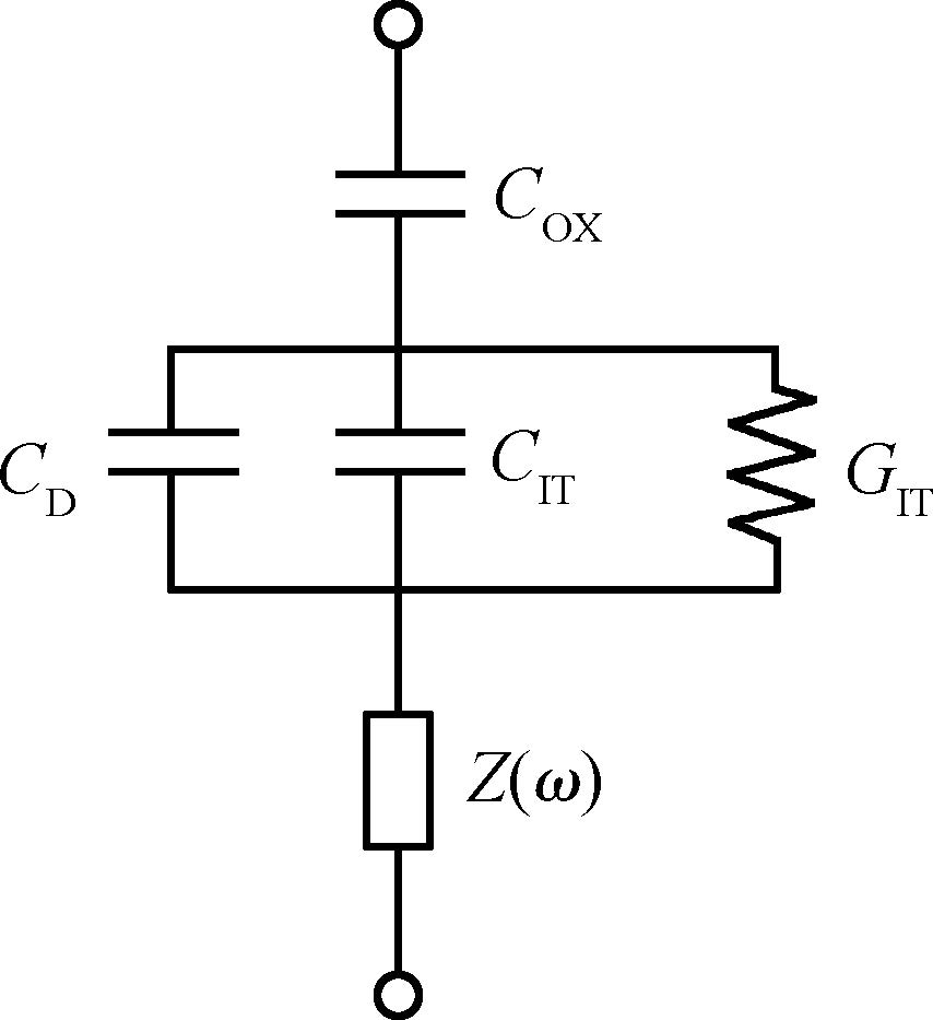
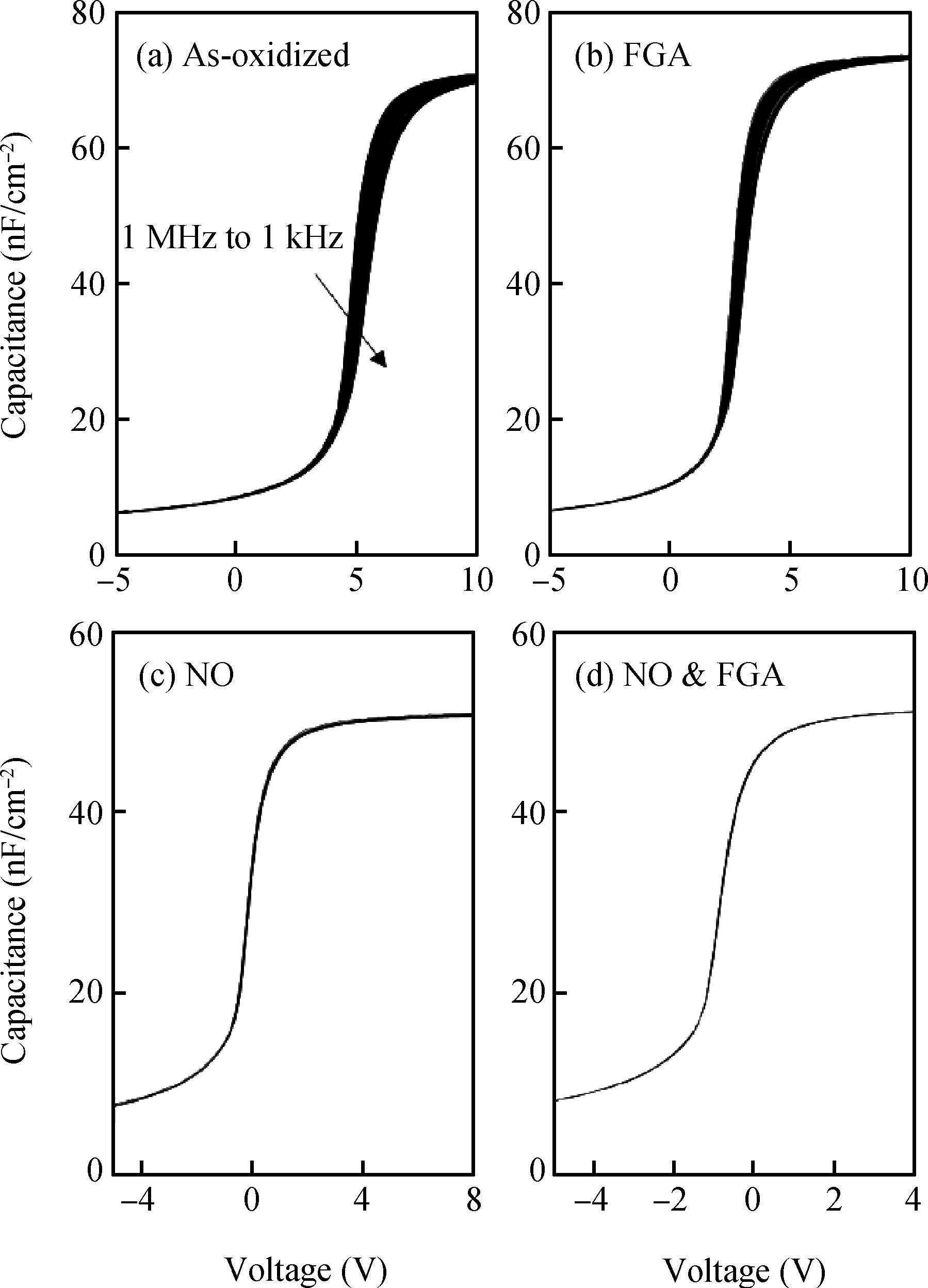
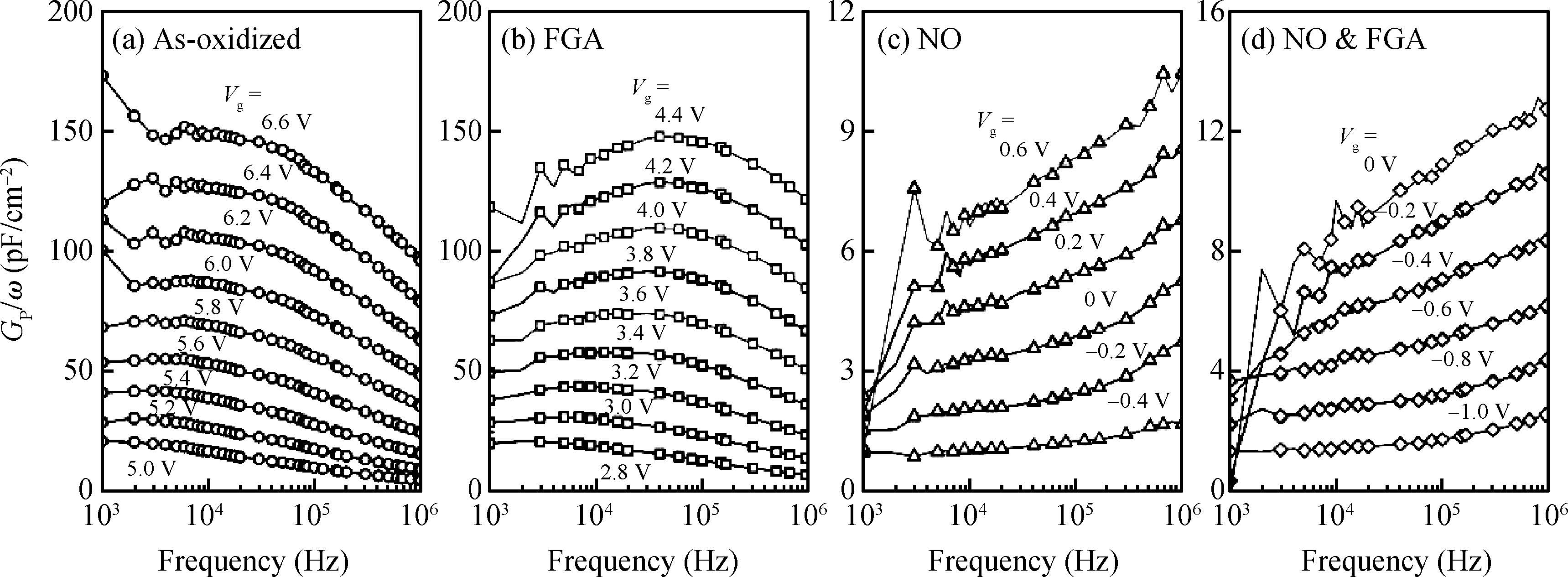
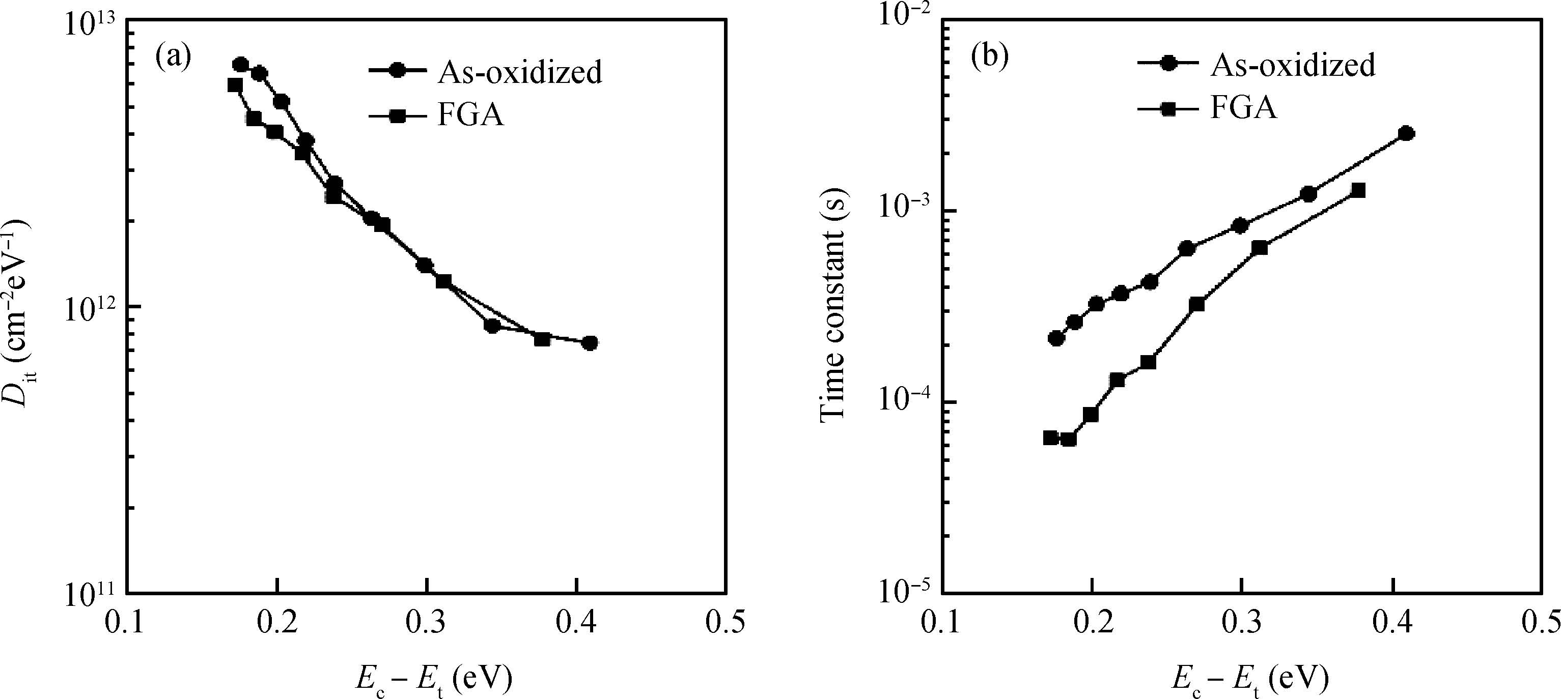
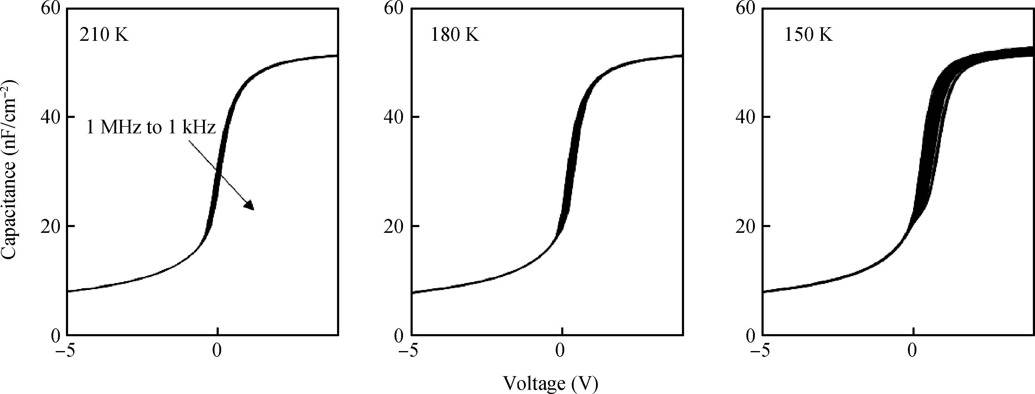
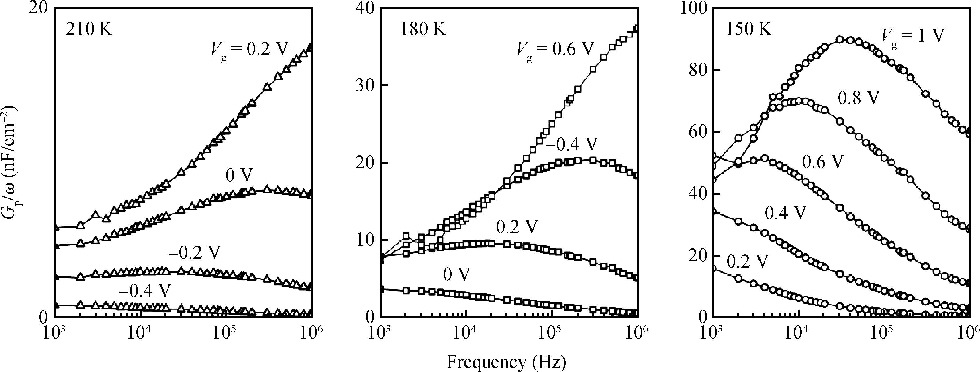
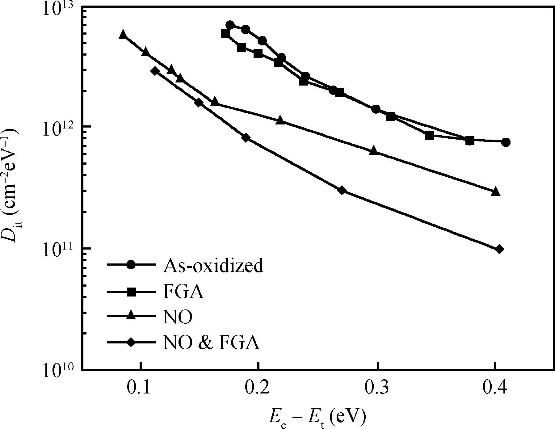
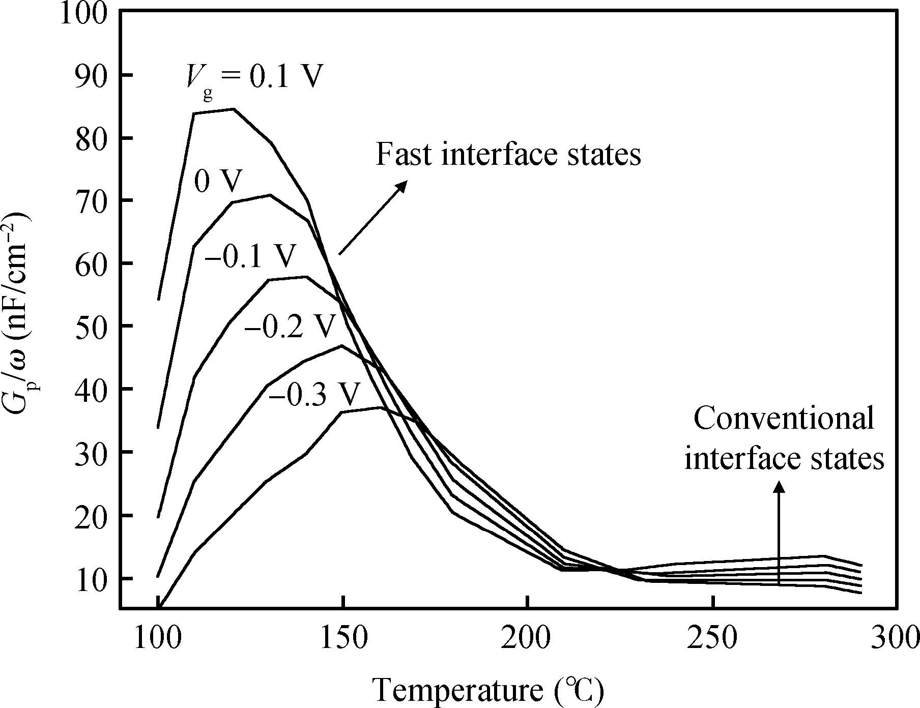
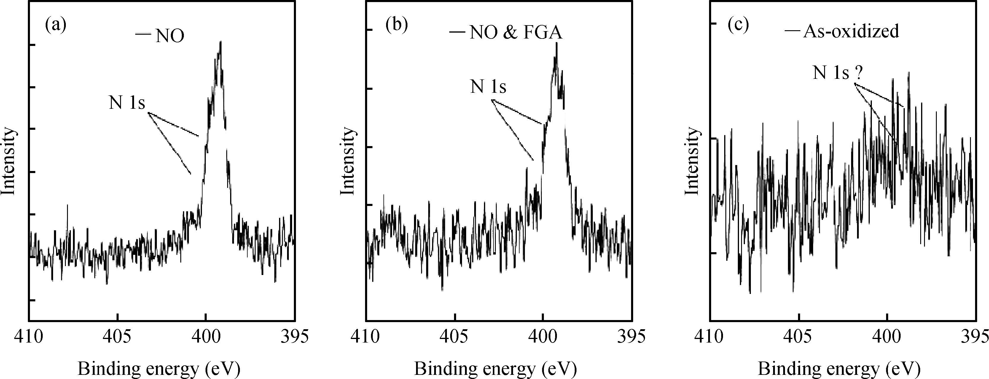
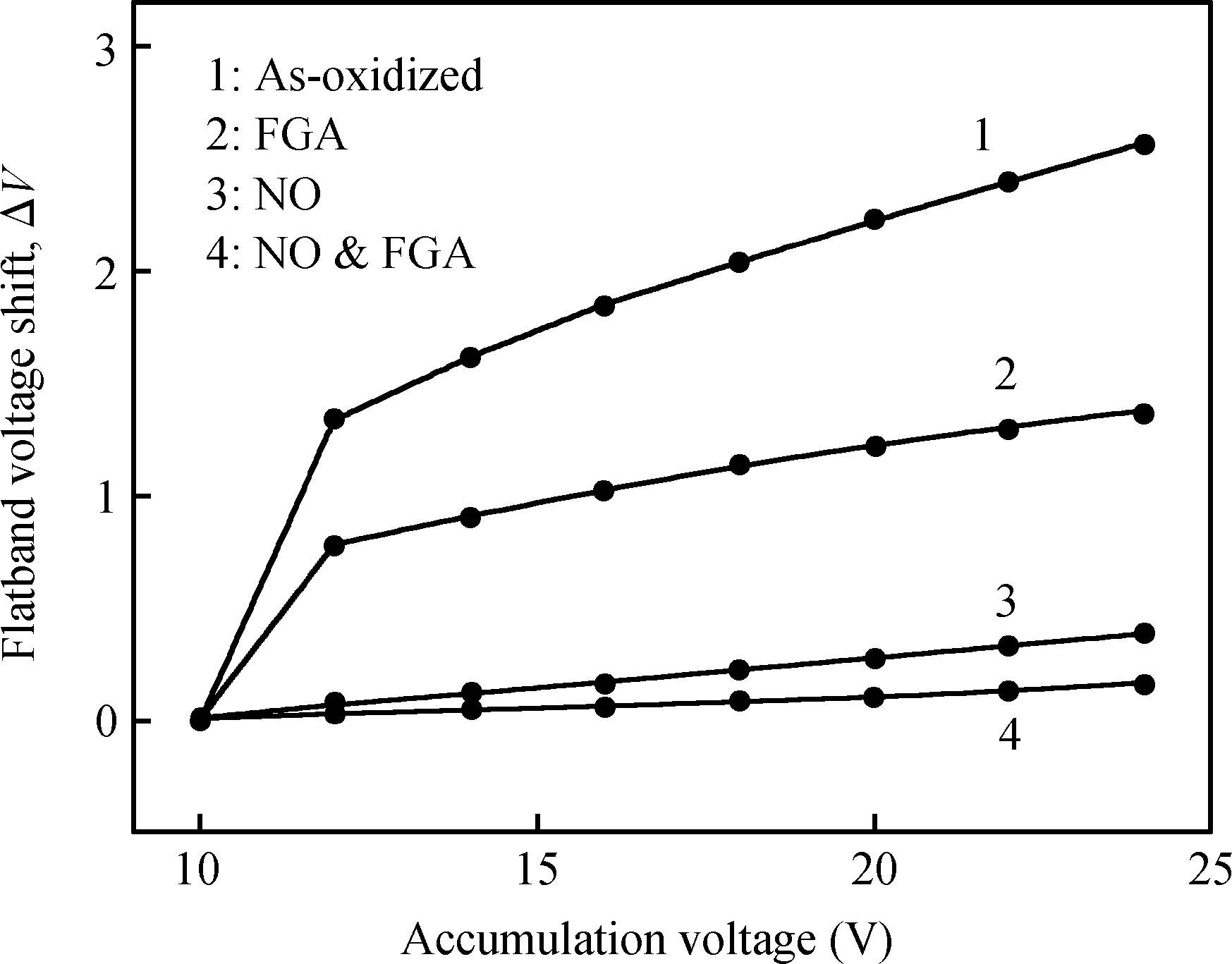
We investigate the effects of NO annealing and forming gas (FG) annealing on the electrical properties of a SiO2/SiC interface by low-temperature conductance measurements. With nitrogen passivation, the density of interface states (DIT) is significantly reduced in the entire energy range, and the shift of flatband voltage, Δ VFB, is effectively suppressed to less than 0.4 V. However, very fast states are observed after NO annealing and the response frequencies are higher than 1 MHz at room temperature. After additional FG annealing, the DIT and Δ VFB are further reduced. The values of the DIT decrease to less than 1011 cm-2 eV-1 for the energy range of EC - ET ≥0.4 eV. It is suggested that the fast states in shallow energy levels originated from the N atoms accumulating at the interface by NO annealing. Though FG annealing has a limited effect on these shallow traps, hydrogen can terminate the residual Si and C dangling bonds corresponding to traps at deep energy levels and improve the interface quality further. It is indicated that NO annealing in conjunction with FG annealing will be a better post-oxidation process method for high performance SiC MOSFETs.
J. Semicond.
2016, 37(2): 026002 doi: 10.1088/1674-4926/37/2/026002

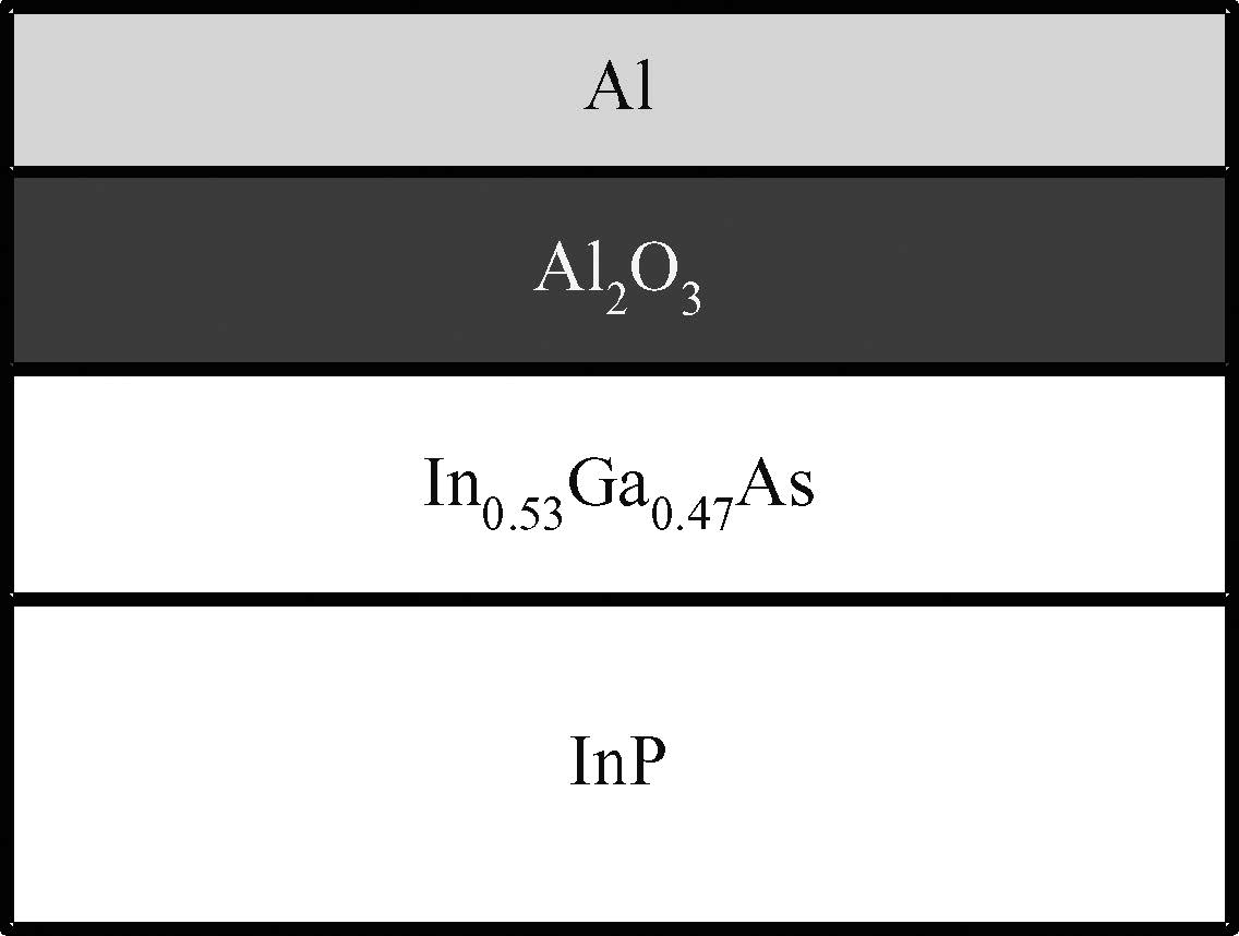
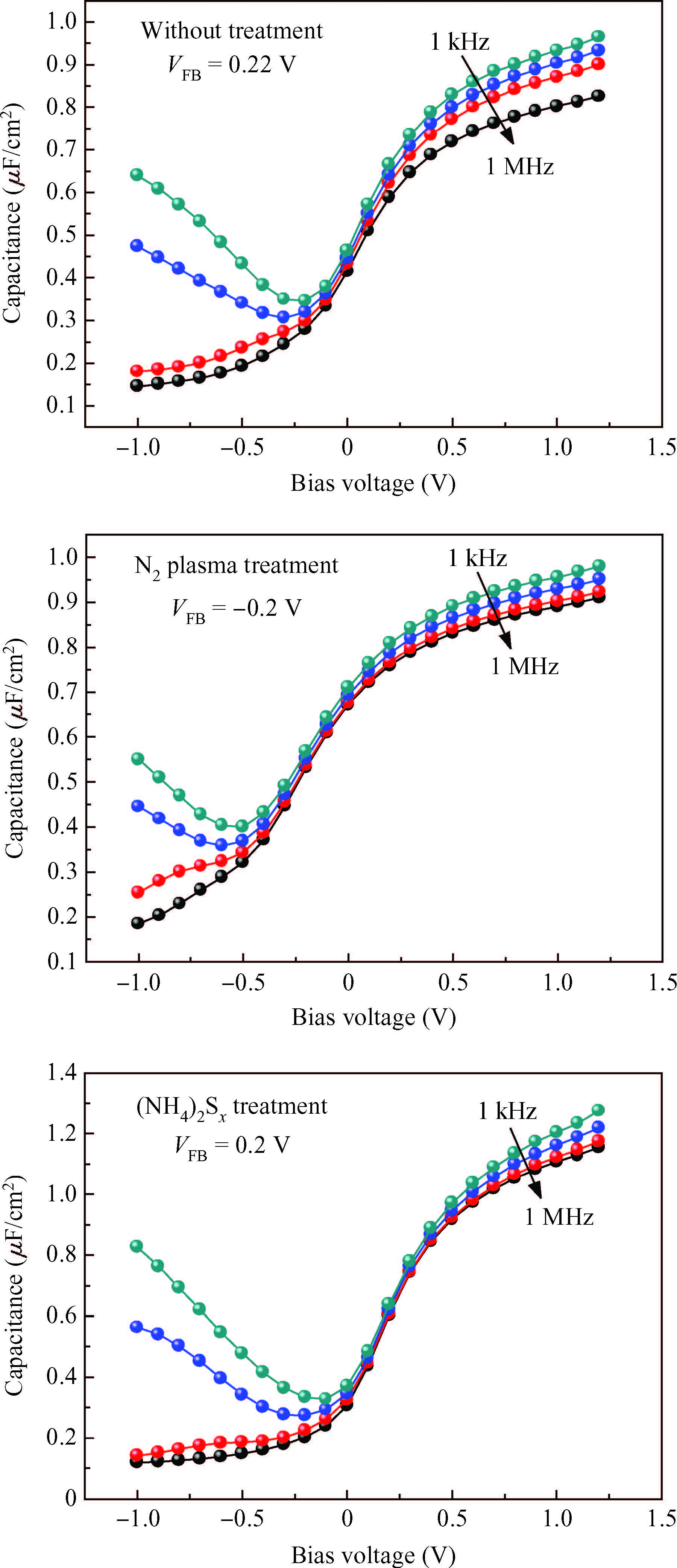
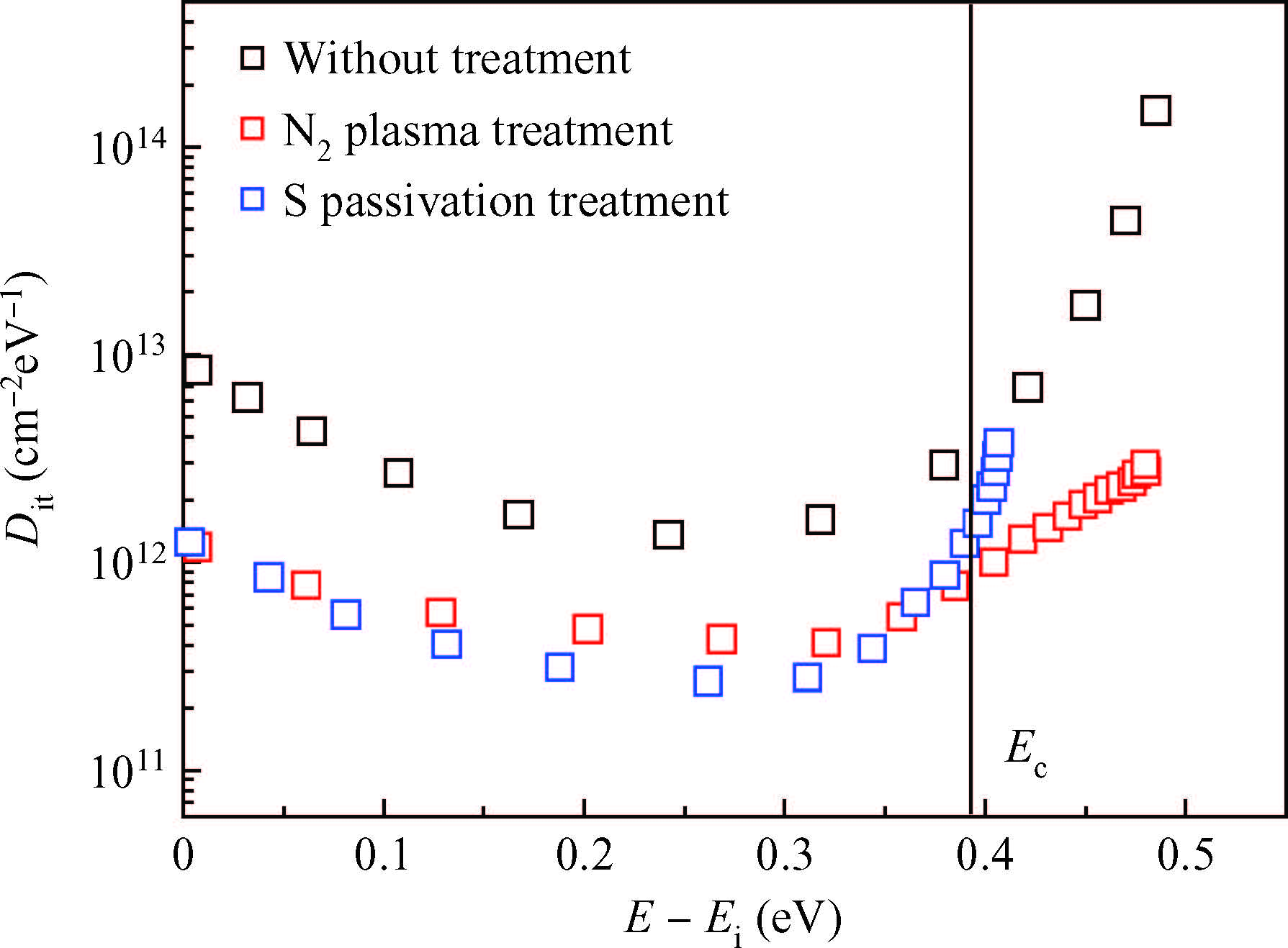
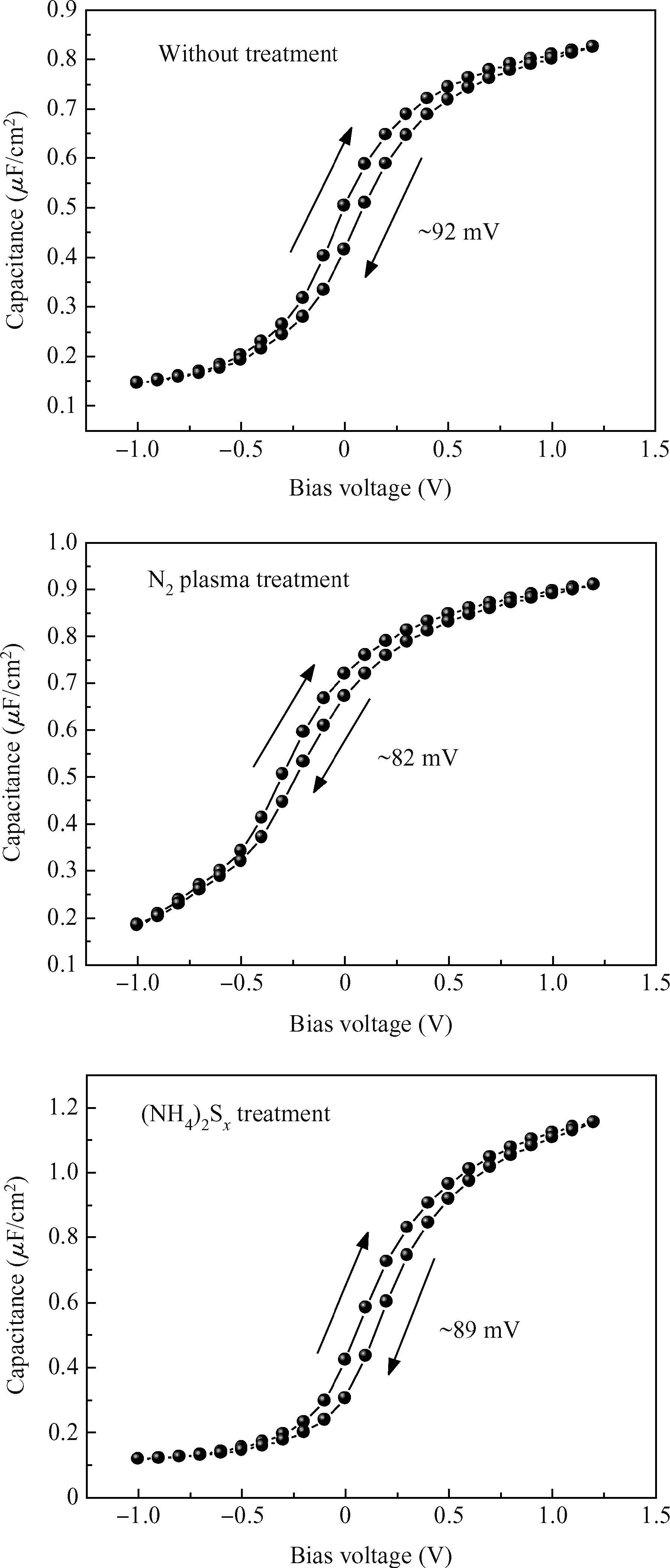
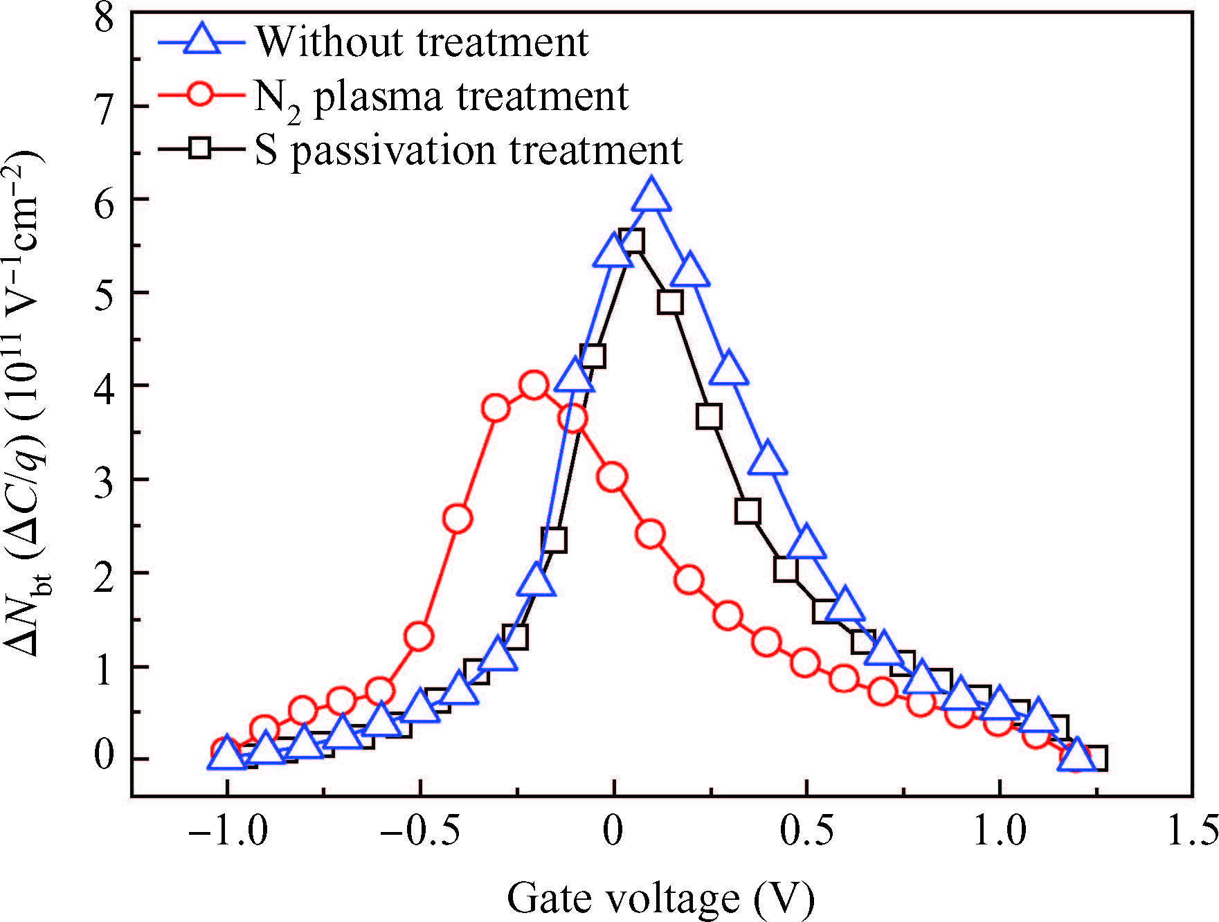
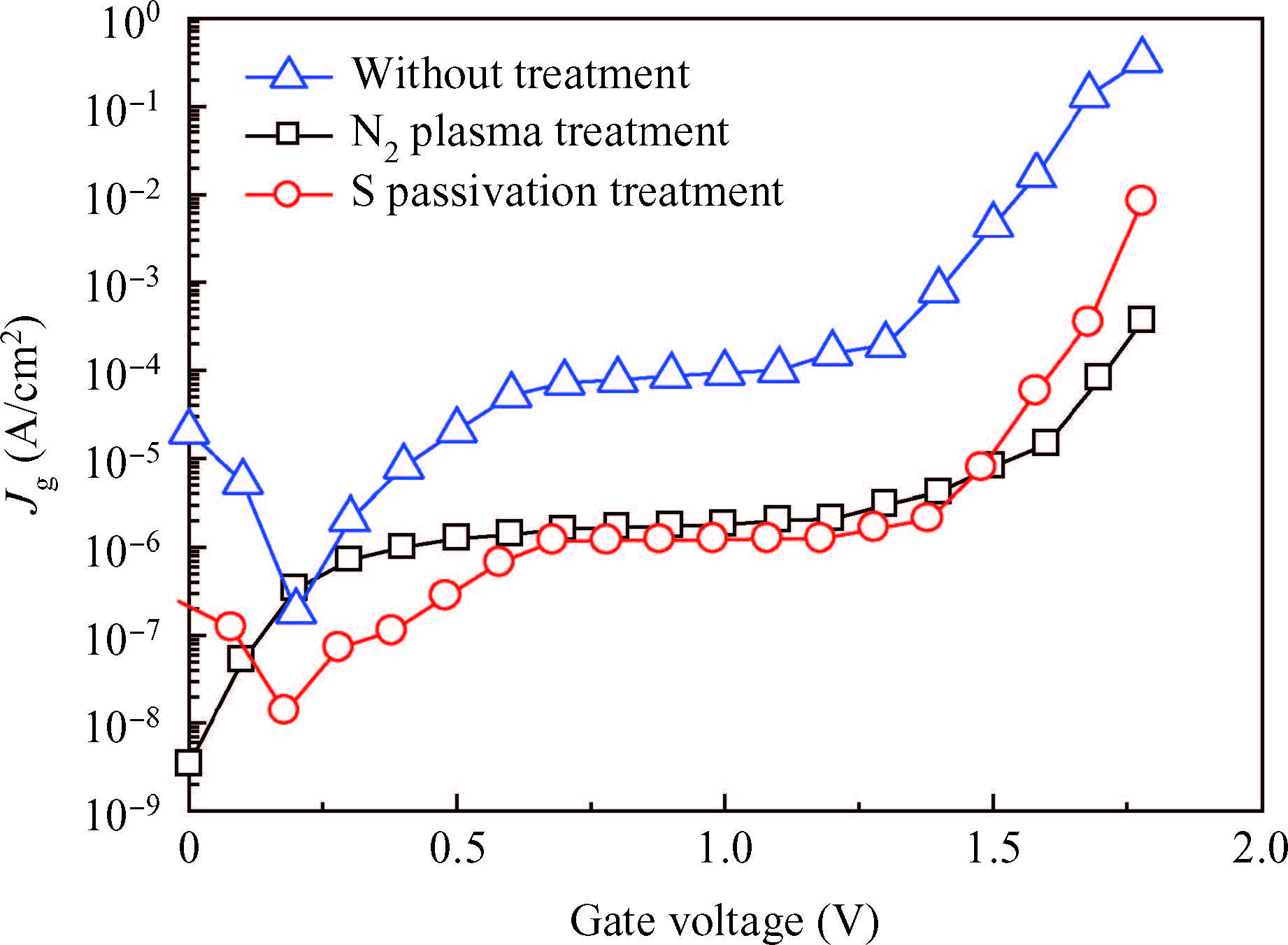
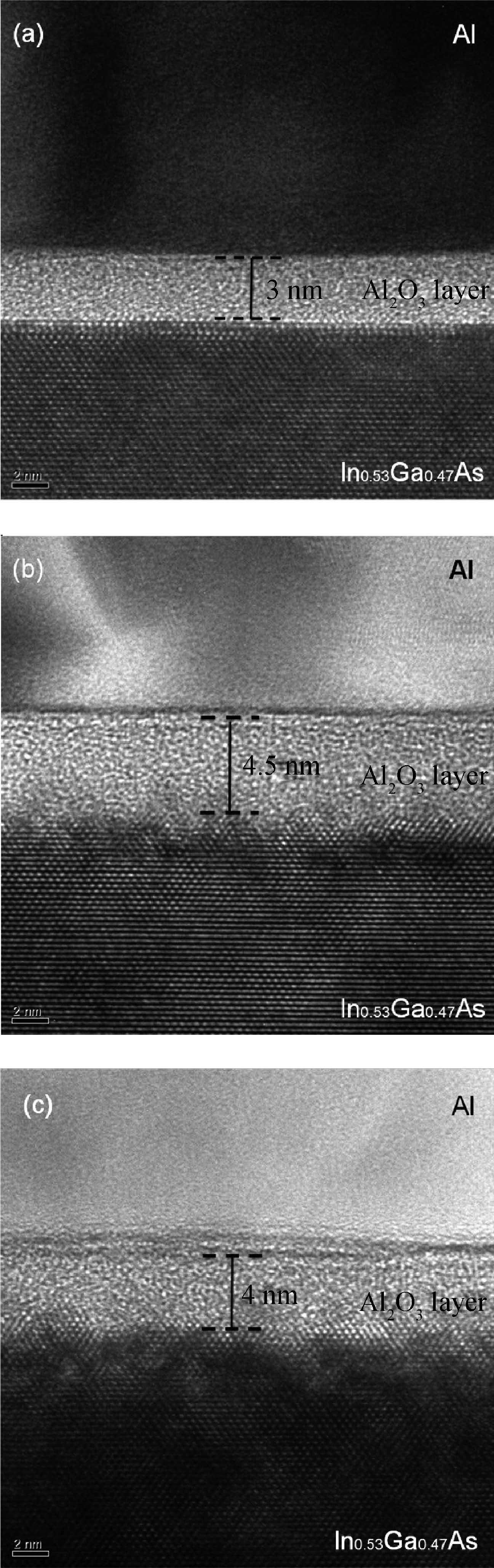
The impact of nitridation and sulfur passivation for In0.53Ga0.47As surfaces on the Al/Al2O3/InGaAs MOS capacitors properties was investigated by comparing the characteristics of frequency dispersion and hysteresis, calculating the Dit and Δ Nbt values, and analyzing the interface traps and the leakage current. The results showed that both of the methods could form a passivation-layer on the InGaAs surface. The samples treated by N2 plasma could obtain good interface properties with the smallest frequency dispersion in the accumulation region, and the best hysteresis characteristics and good I-V properties were presented. Also the samples with (NH4)2Sx treatment showed the smallest frequency dispersion near the flat-band region and a minimum Dit value of 2.6 × 1011 cm-2 eV-1.
J. Semicond.
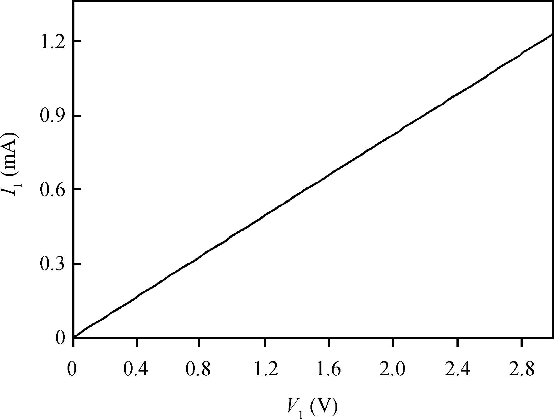
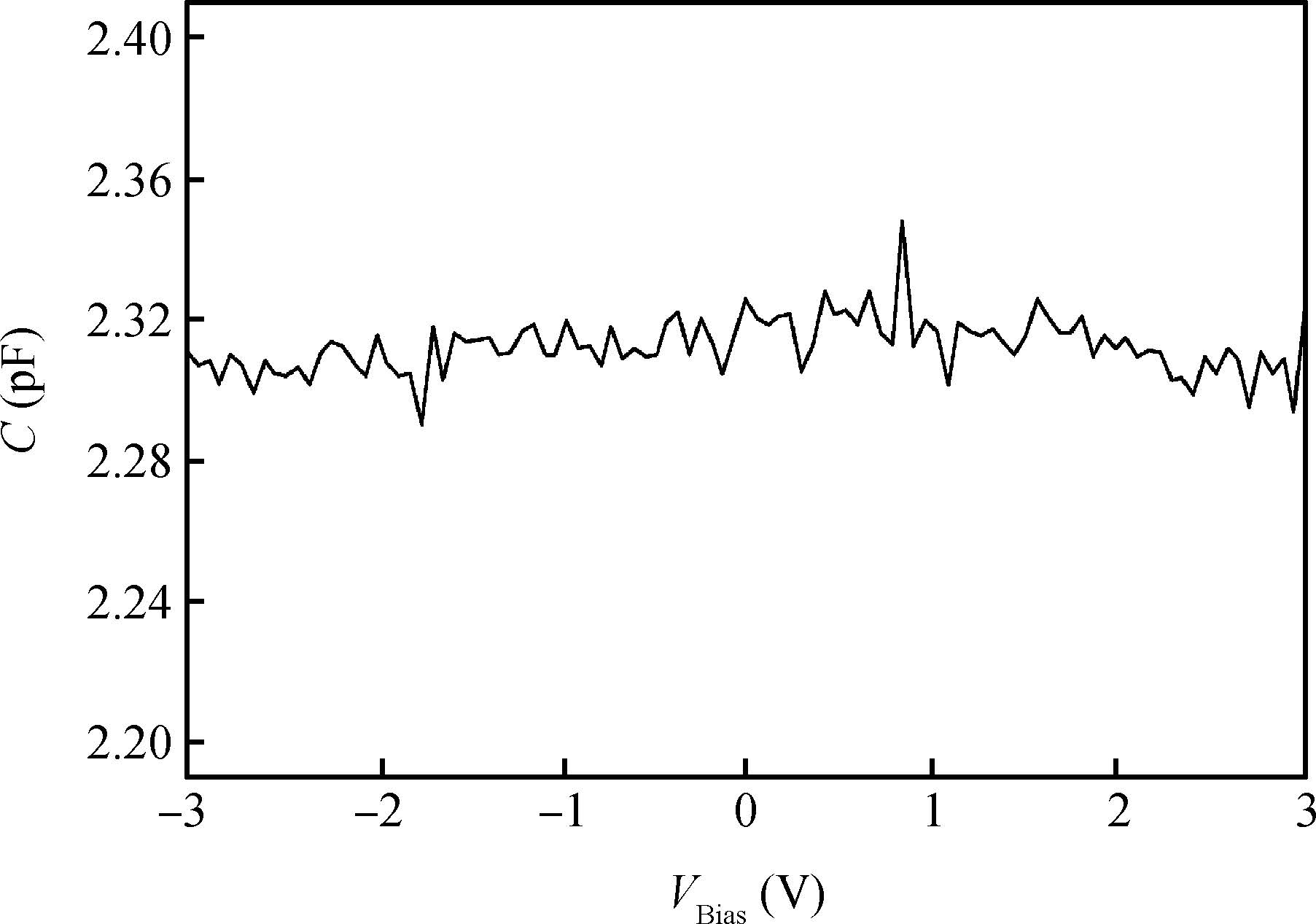
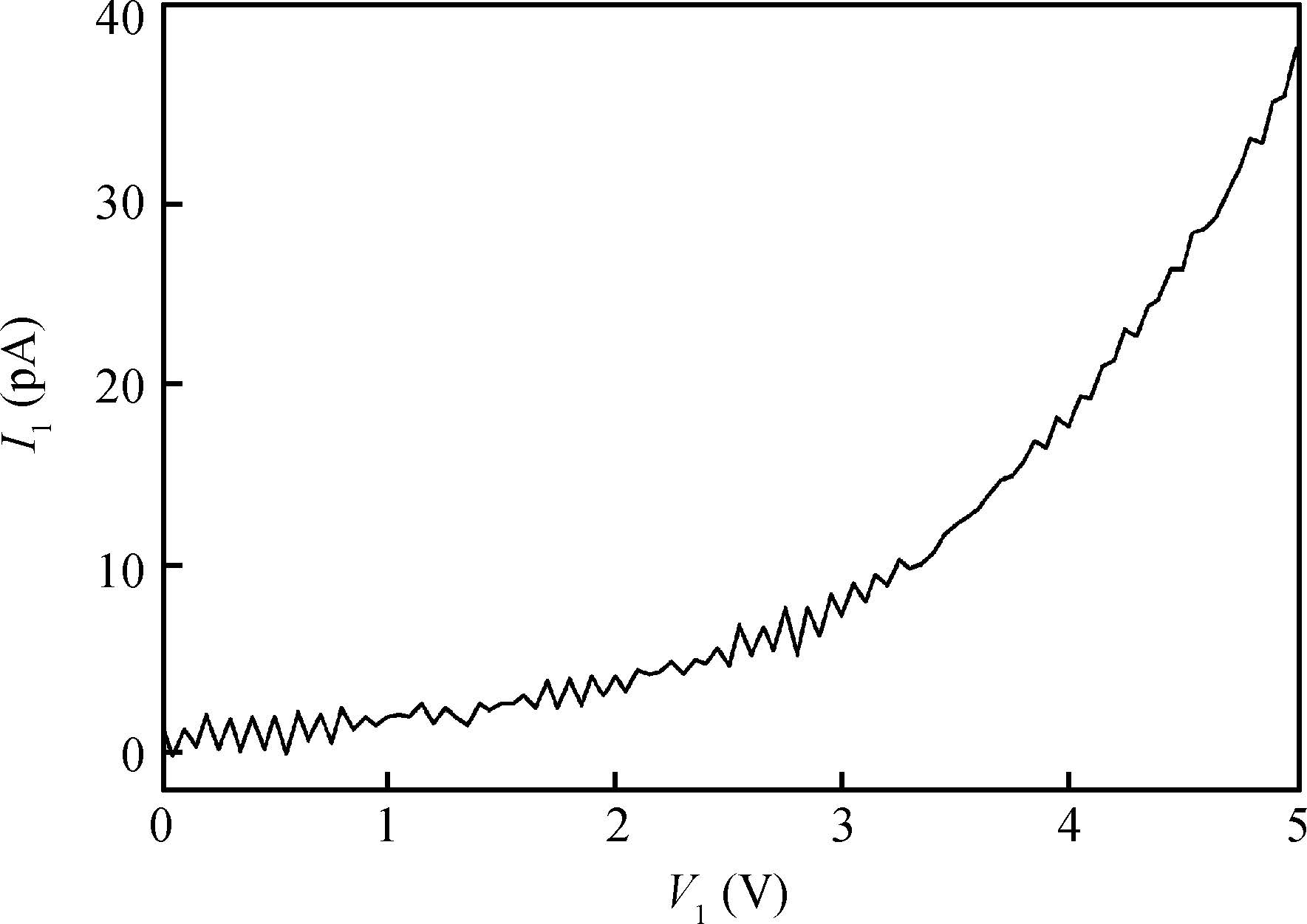
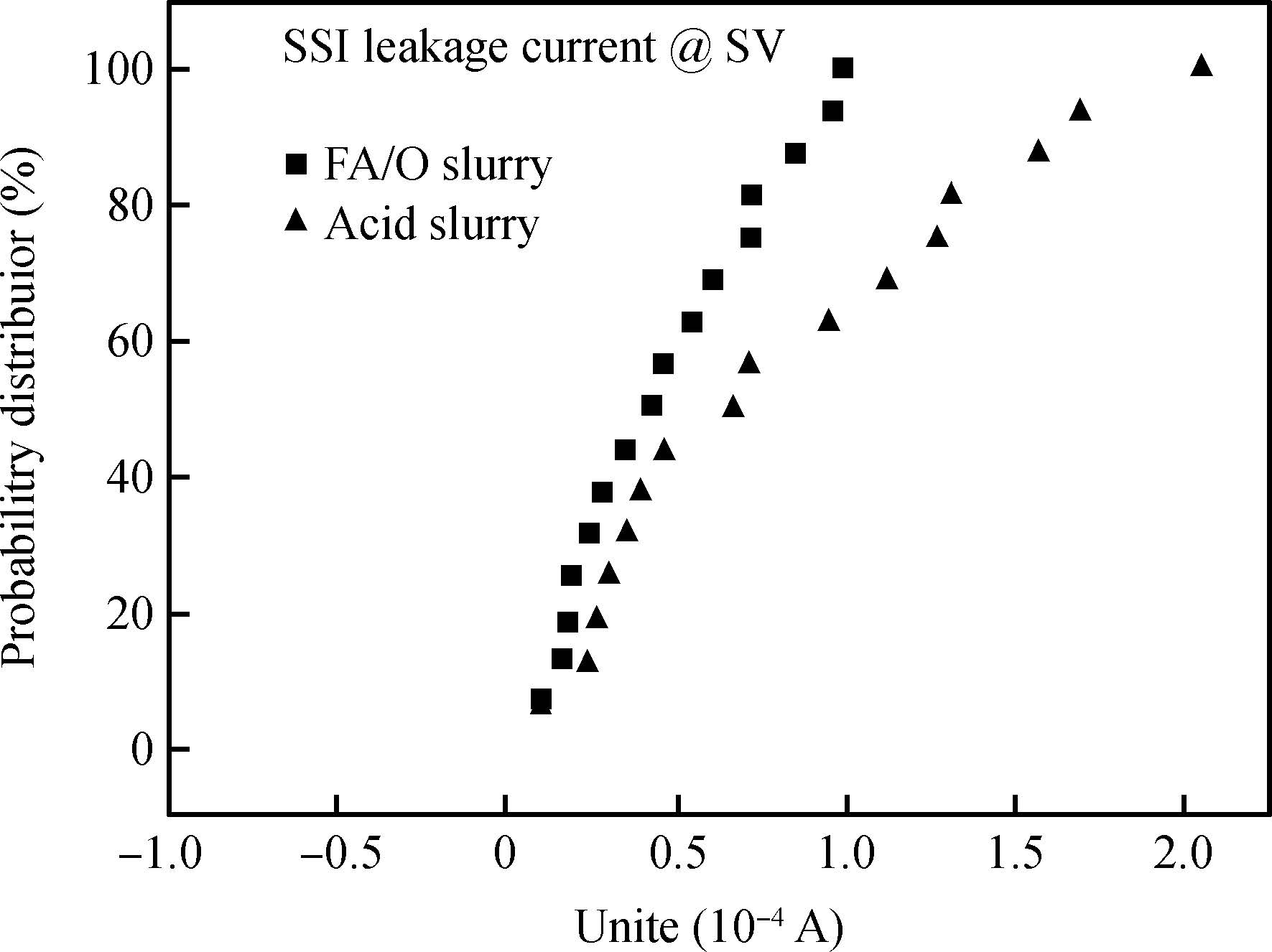
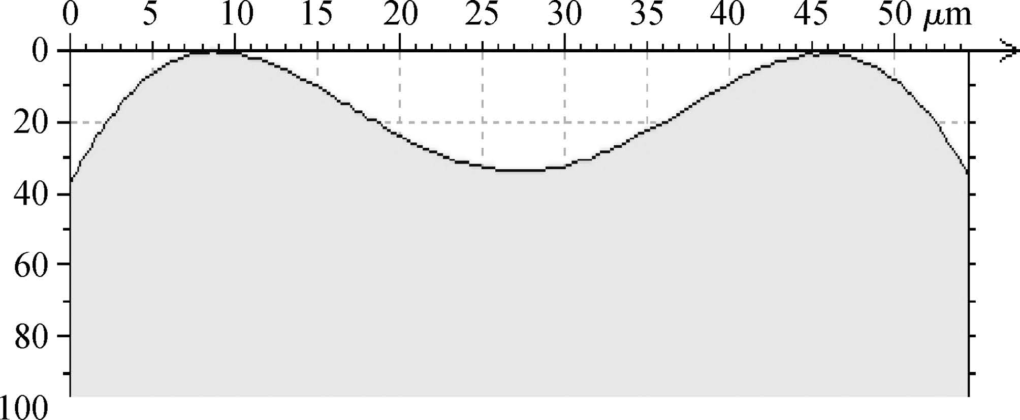
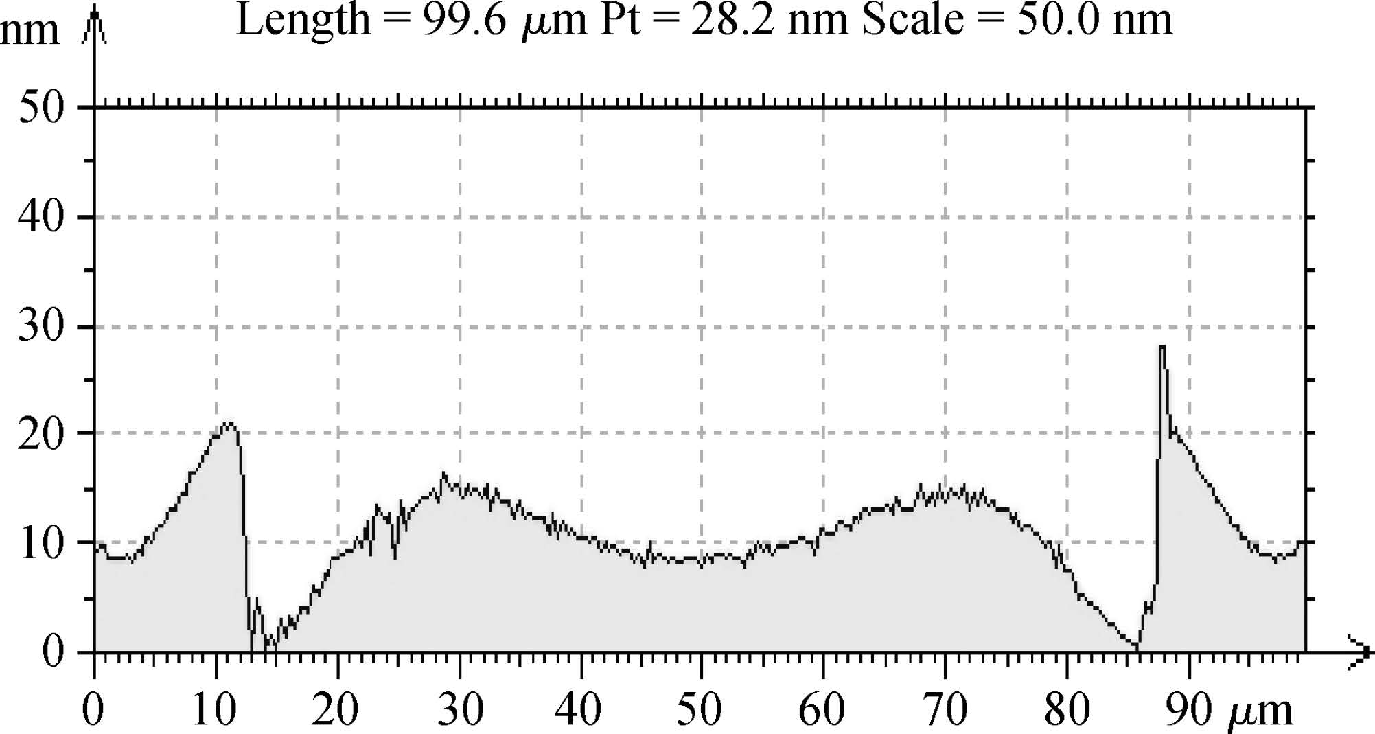
2016, 37(2): 026003 doi: 10.1088/1674-4926/37/2/026003
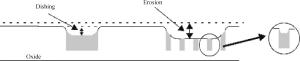
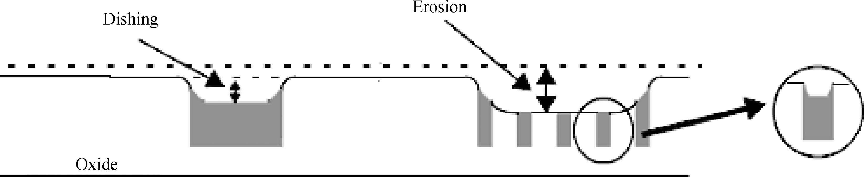
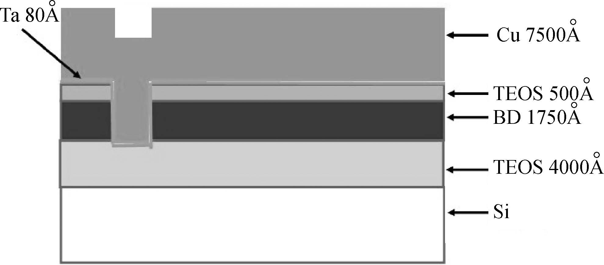
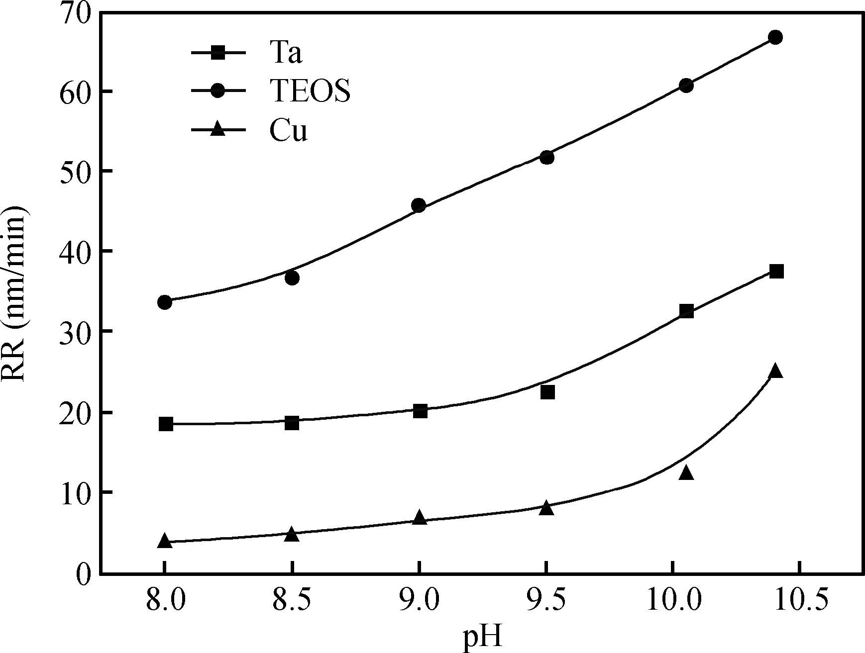
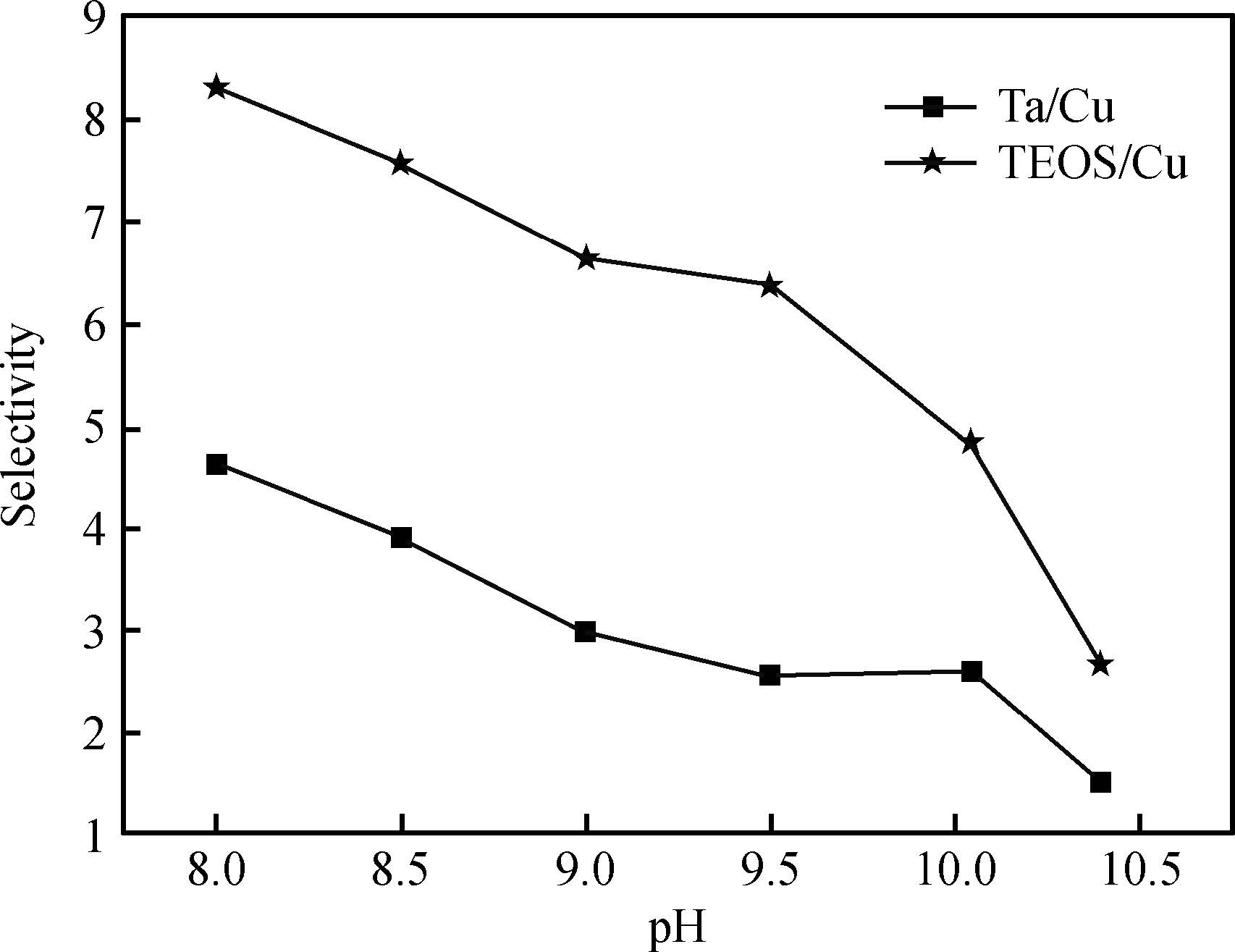
Because the polishing of different materials is required in barrier chemical mechanical planarization (CMP) processes, the development of a kind of barrier slurry with improved removal rate selectivity for Cu/barrier/TEOS would reduce erosion and dishing defects on patterned Cu wafers. In this study, we developed a new benzotriazole-free barrier slurry named FA/O barrier slurry, containing 20 mL/L of the chelating agent FA/O, 5 mL/L surfactant, and a 1:5 concentration of abrasive particles. By controlling the polishing slurry ingredients, the removal rate of different materials could be controlled. For process integration considerations, the effect of the FA/O barrier slurry on the dielectric layer of the patterned Cu wafer was investigated. After CMP processing by the FA/O barrier slurry, the characteristics of the dielectric material were tested. The results showed that the dielectric characteristics met demands for industrial production. The current leakage was of pA scale. The resistance and capacitance were 2.4 kΩ and 2.3 pF, respectively. The dishing and erosion defects were both below 30 nm in size. CMP-processed wafers using this barrier slurry could meet industrial production demands.