Issue Browser
Volume 41, Issue 5,
May 2020
Column
J. Semicond.
2020, 41(5): 051201 doi: 10.1088/1674-4926/41/5/051201
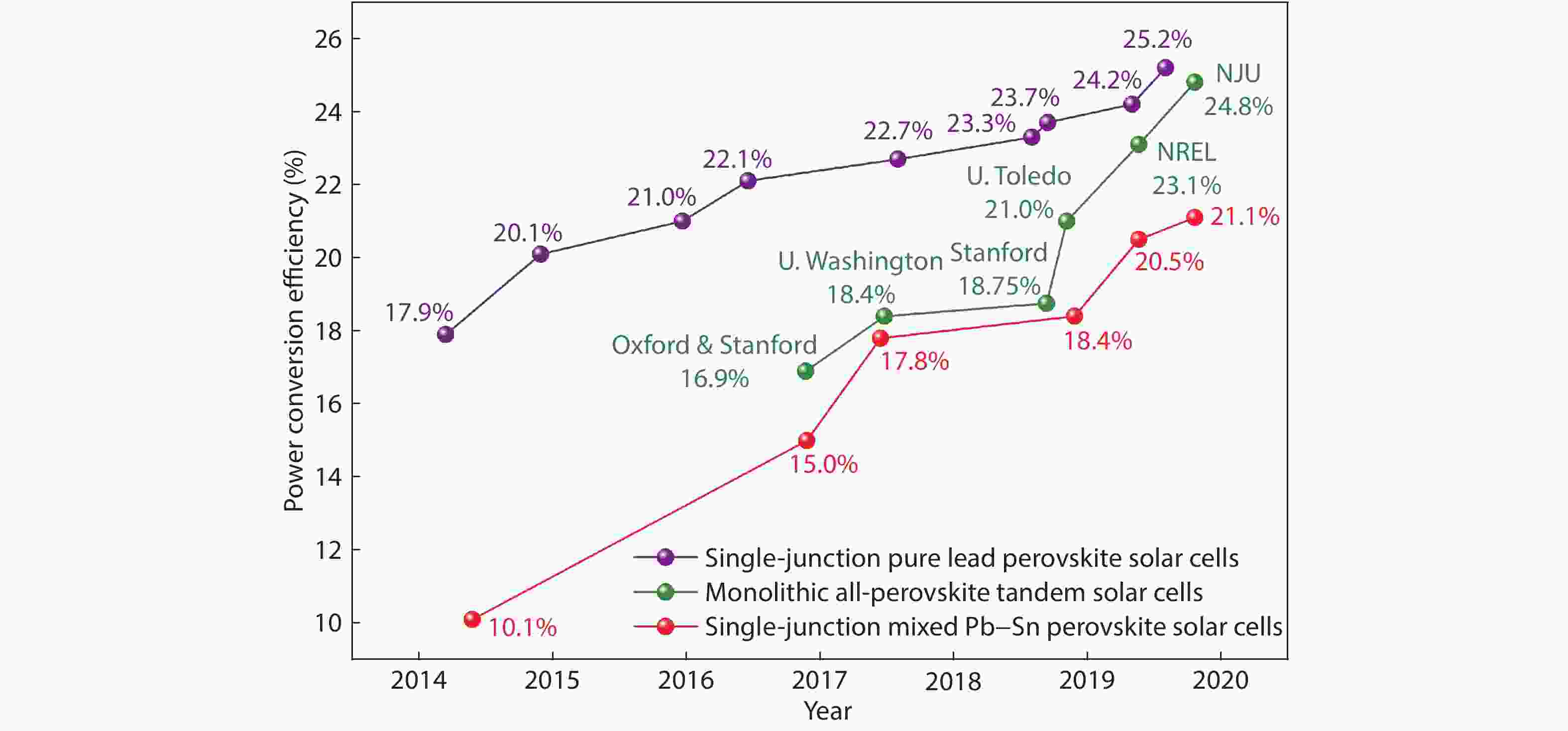
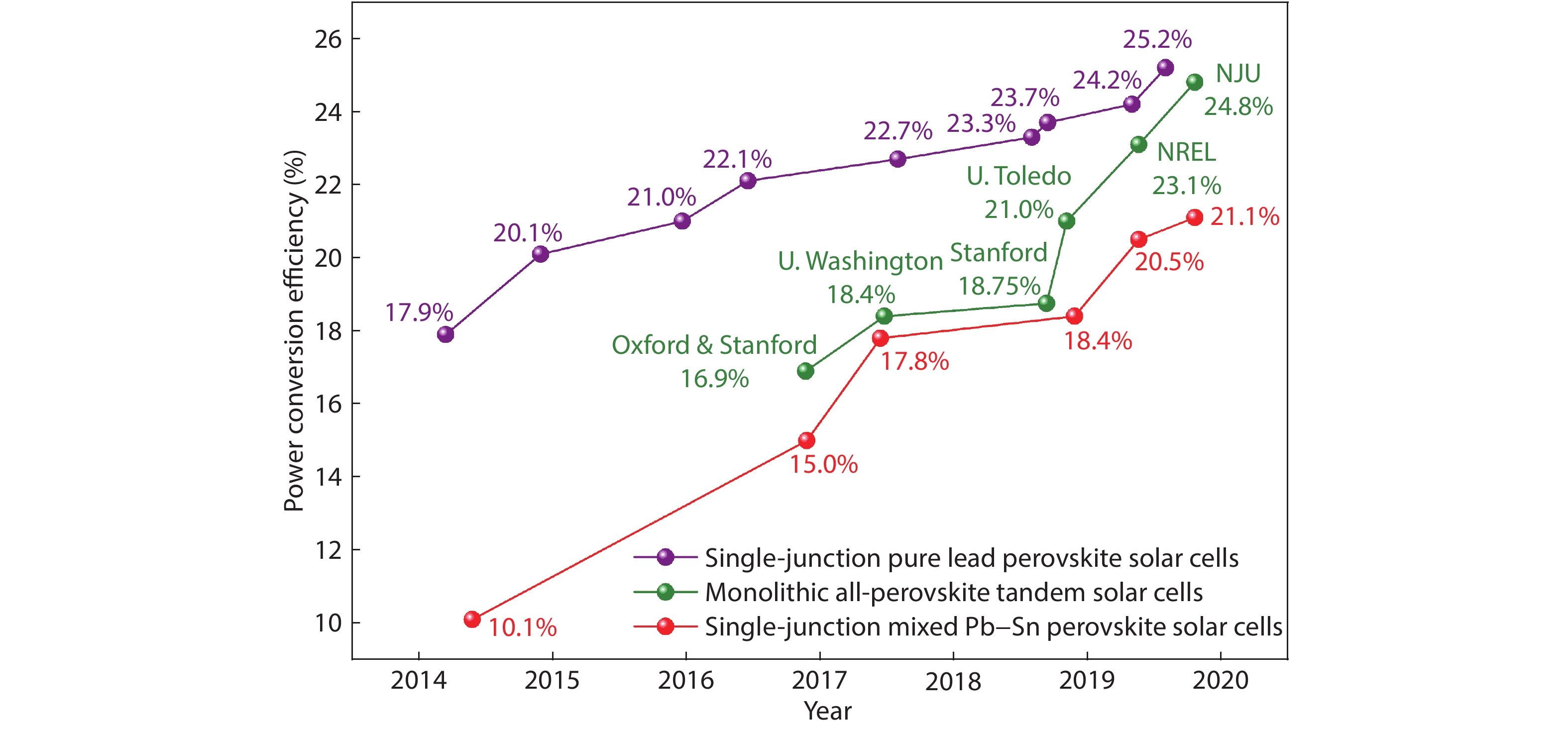
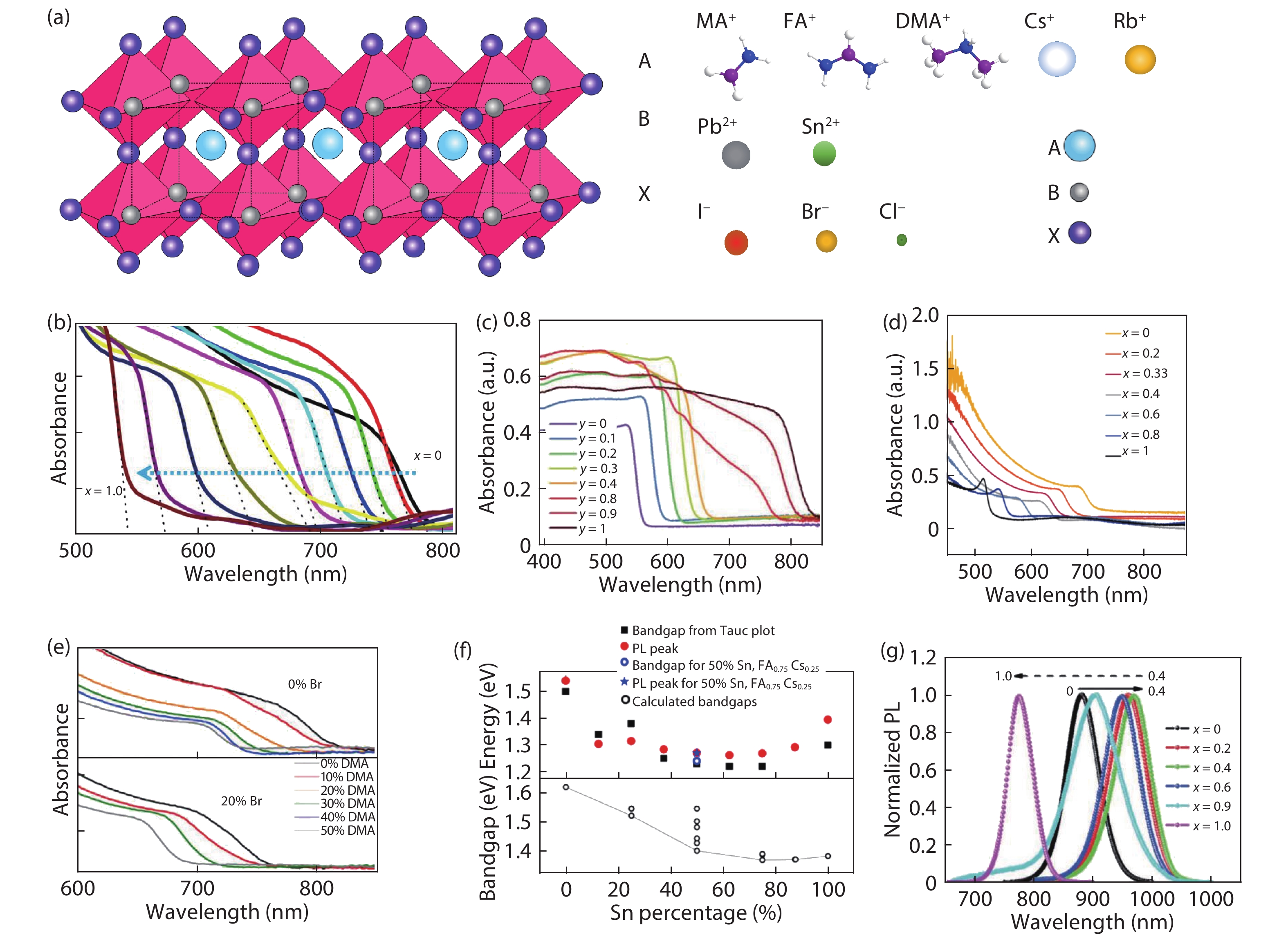
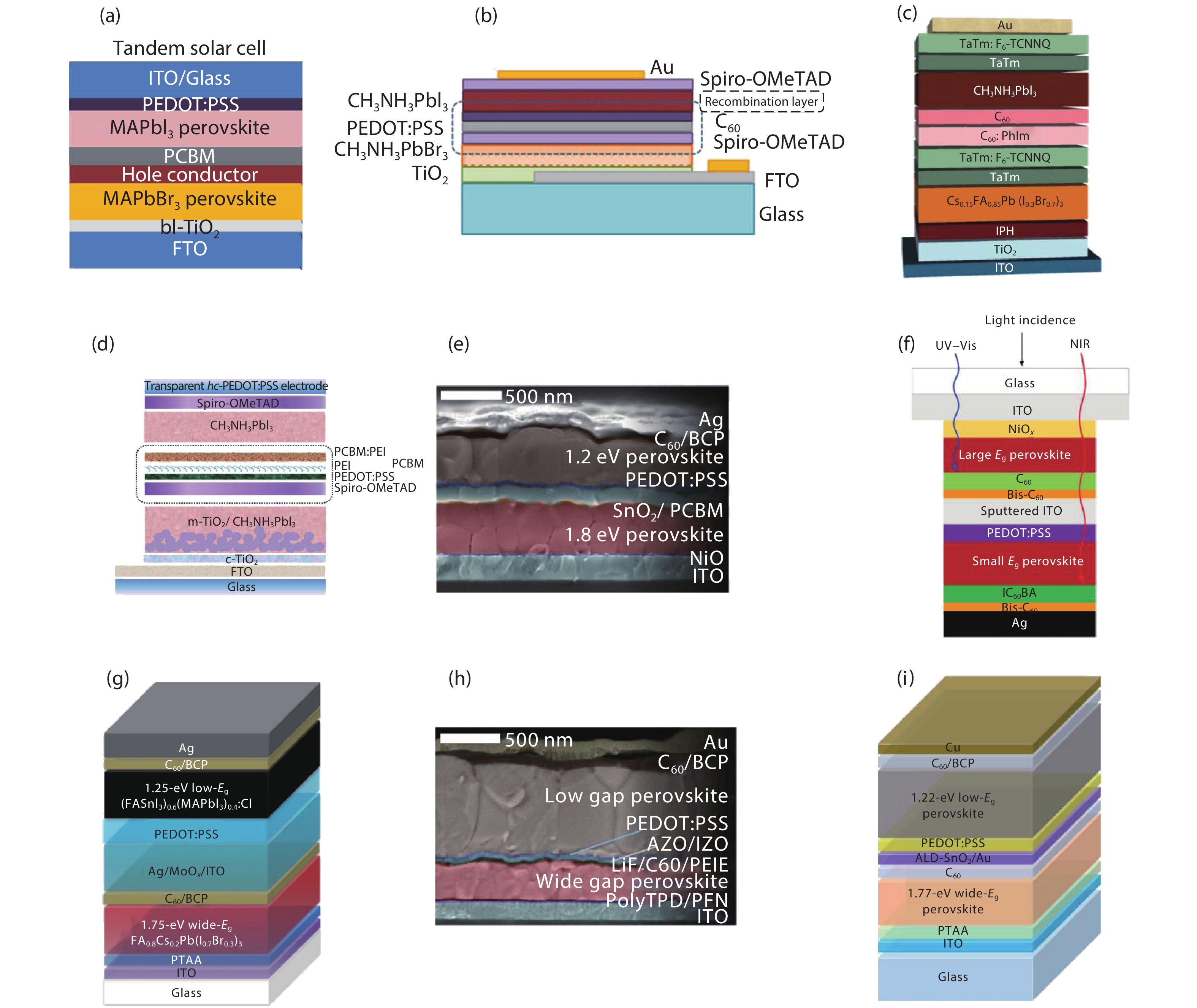
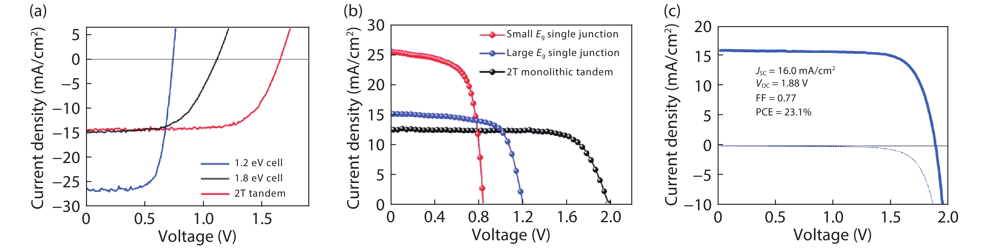
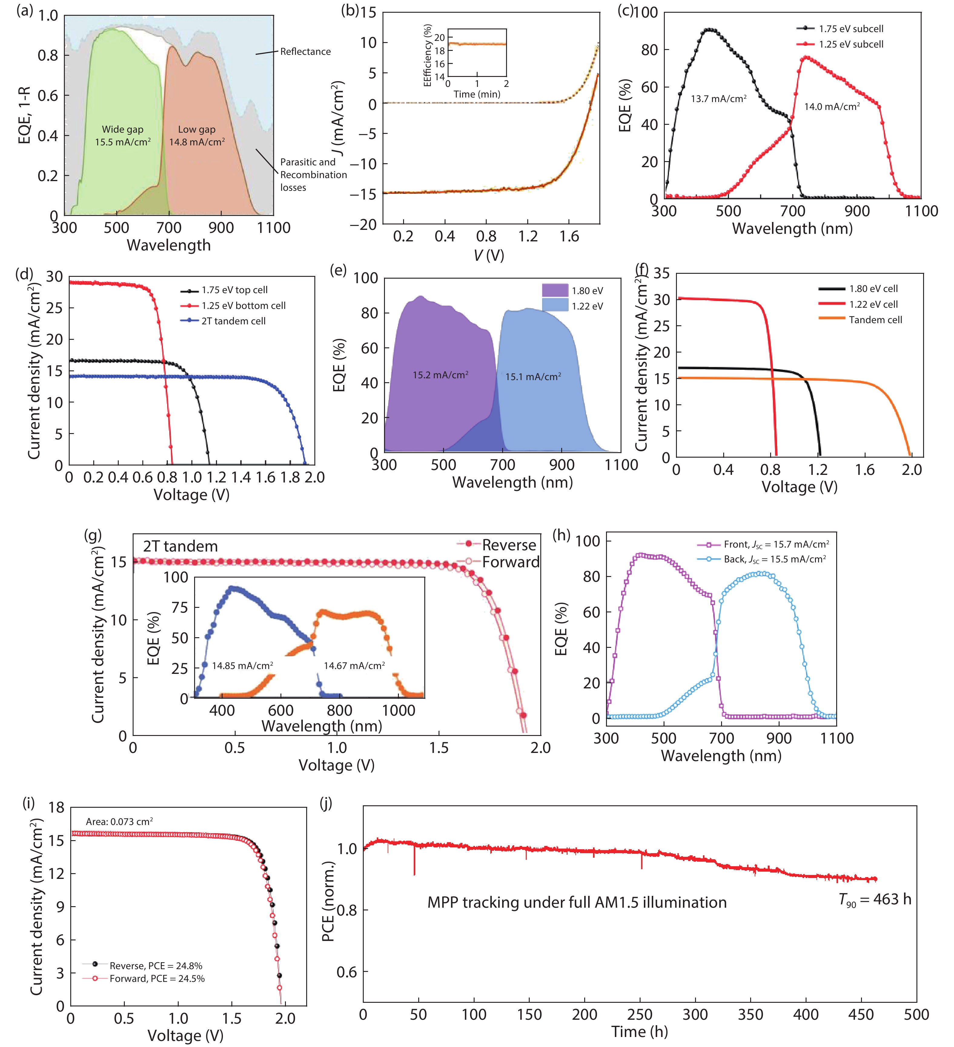
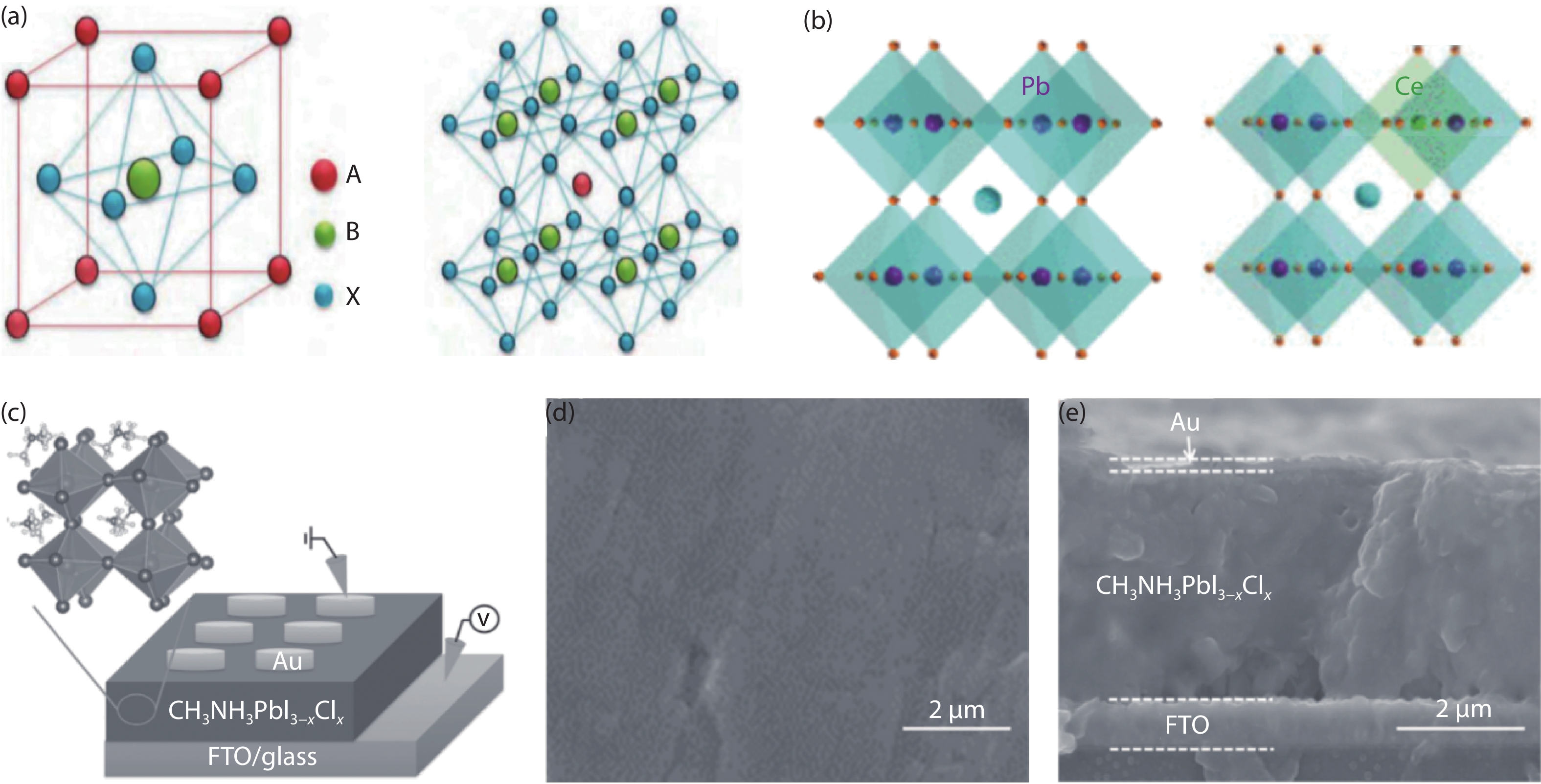
Organic–inorganic halide perovskites have received widespread attention thanks to their strong light absorption, long carrier diffusion lengths, tunable bandgaps, and low temperature processing. Single-junction perovskite solar cells (PSCs) have achieved a boost of the power conversion efficiency (PCE) from 3.8% to 25.2% in just a decade. With the continuous growth of PCE in single-junction PSCs, exploiting of monolithic all-perovskite tandem solar cells is now an important strategy to go beyond the efficiency available in single-junction PSCs. In this review, we first introduce the structure and operation mechanism of monolithic all-perovskite tandem solar cell. We then summarize recent progress in monolithic all-perovskite tandem solar cells from the perspectives of different structural units in the device: tunnel recombination junction, wide-bandgap top subcell, and narrow-bandgap bottom subcell. Finally, we provide our insights into the challenges and scientific issues remaining in this rapidly developing research field.

J. Semicond.
2020, 41(5): 051202 doi: 10.1088/1674-4926/41/5/051202
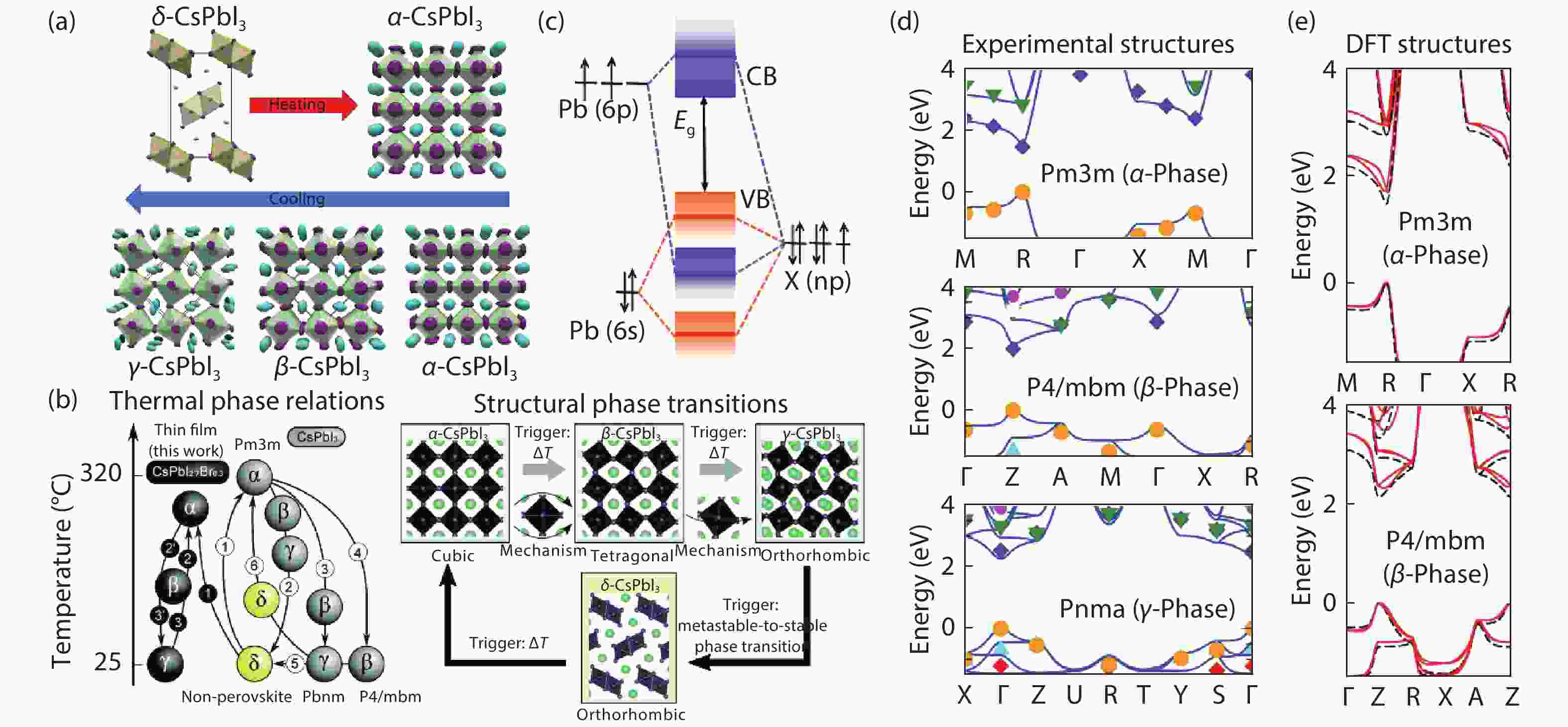
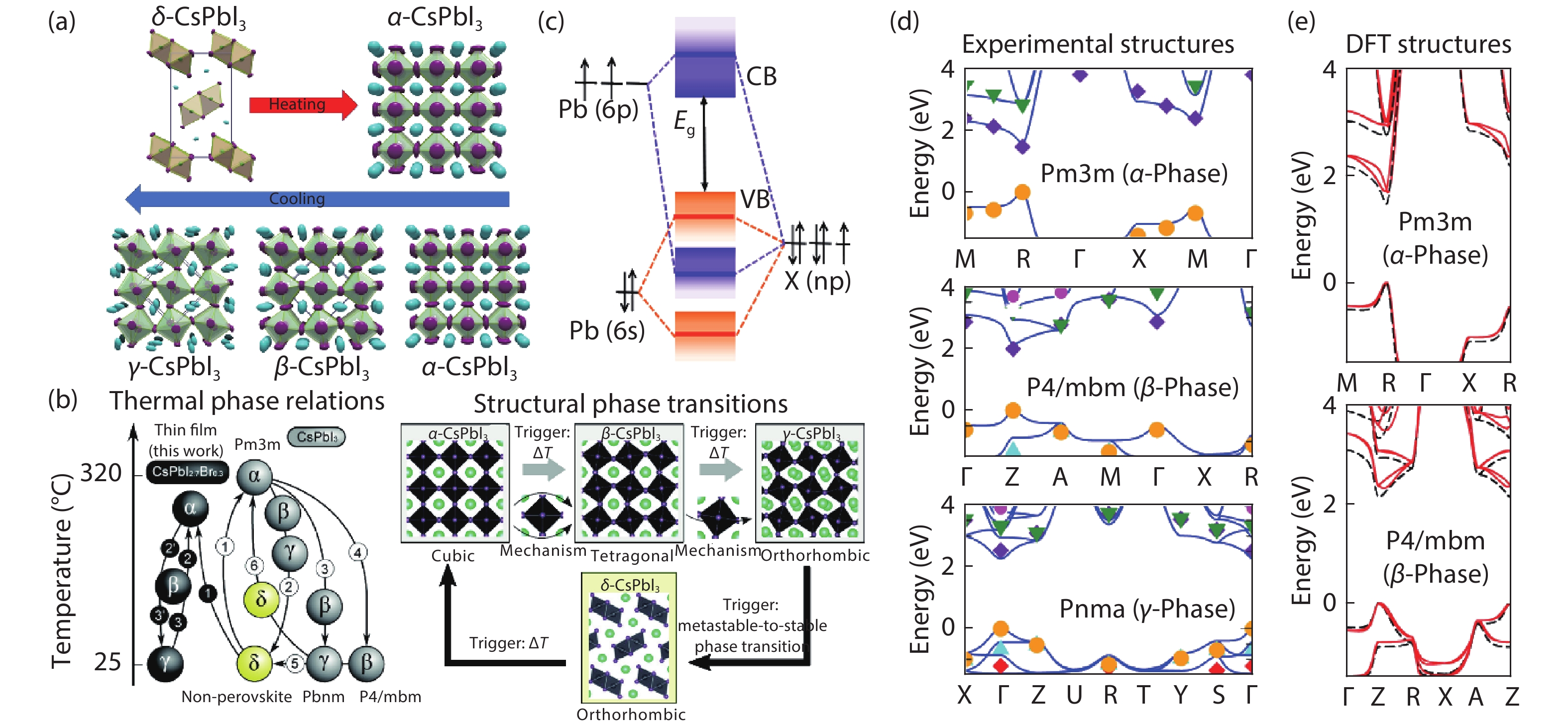
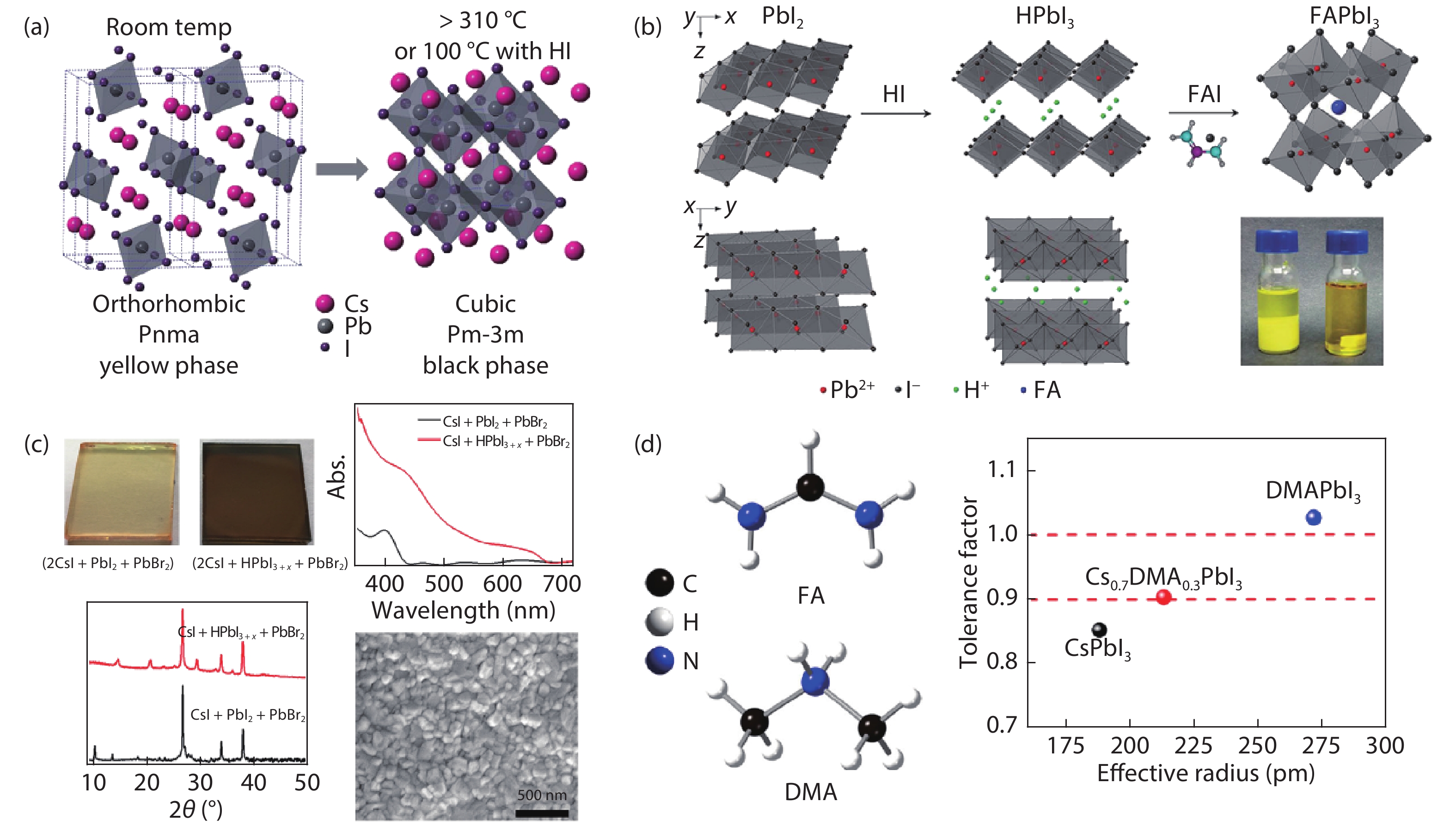
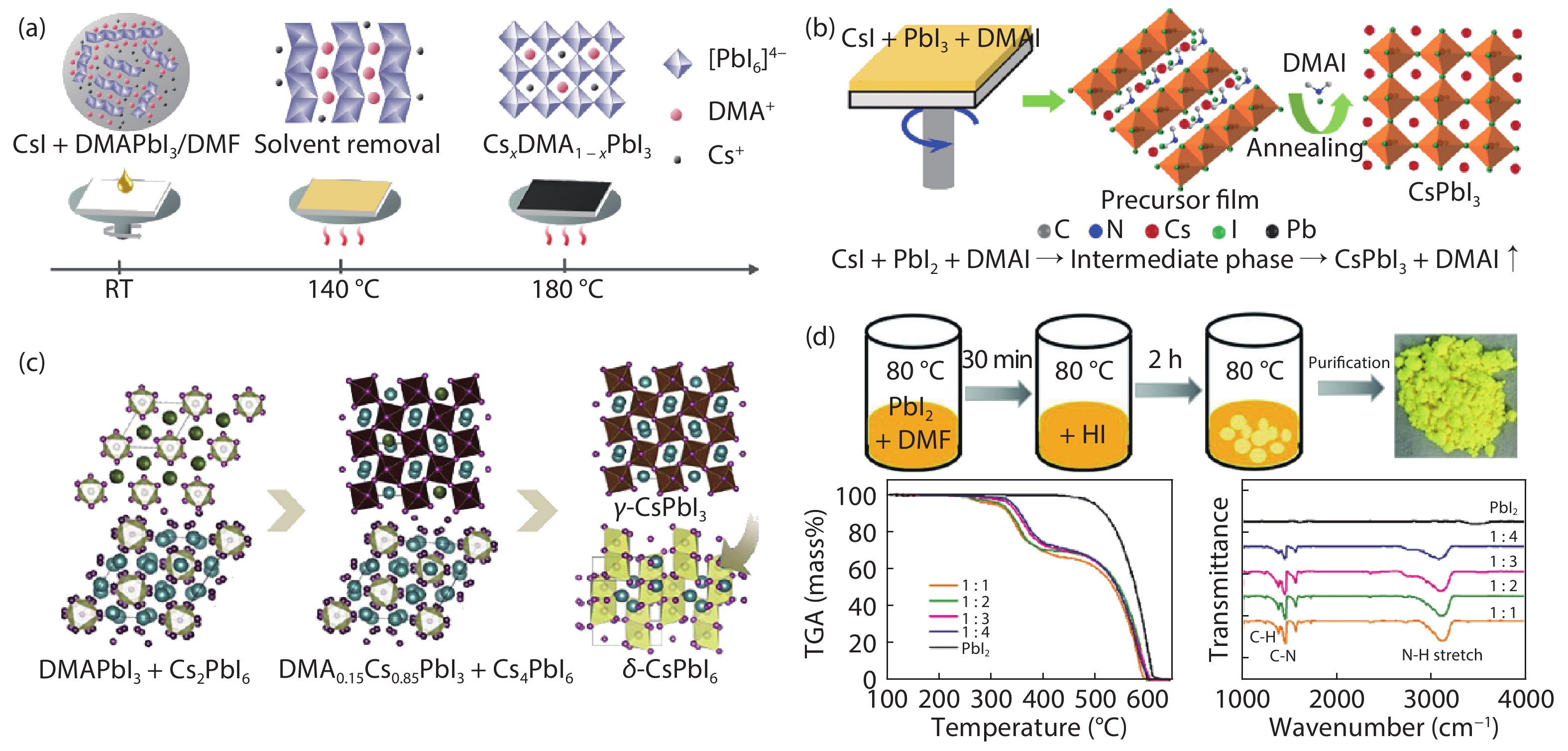
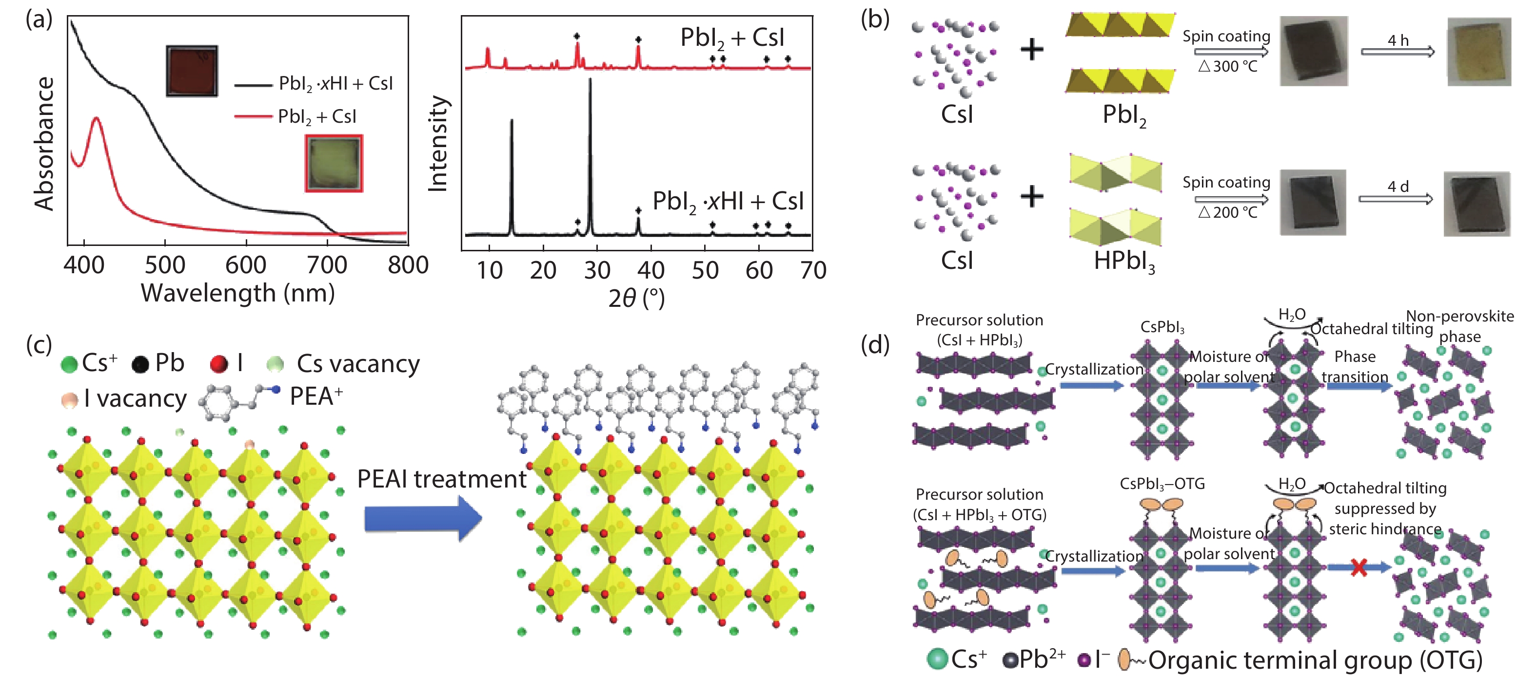
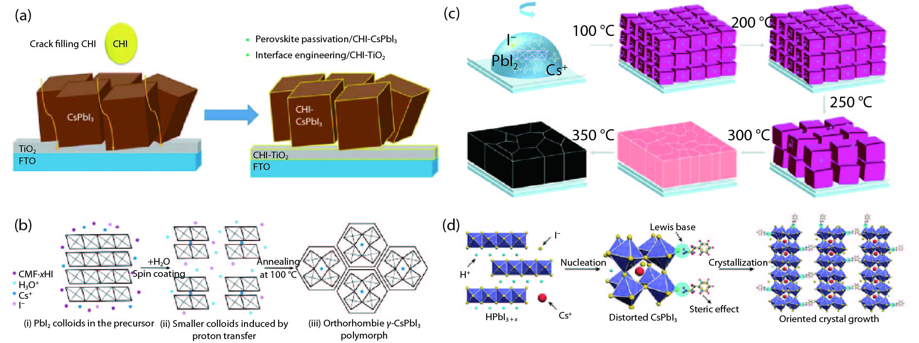
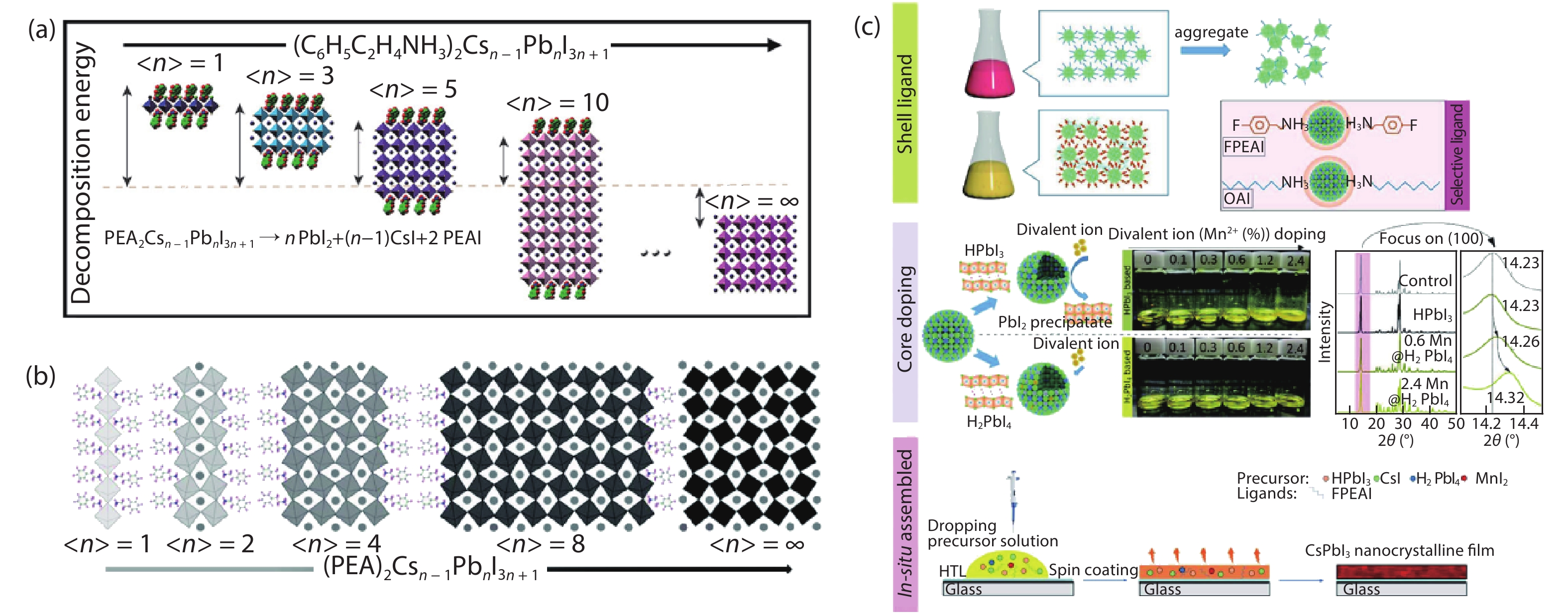
Nowadays, inorganic CsPbI3 perovskite solar cells (PSCs) have become one of the most attractive research hotspots in photovoltaic field for its superior chemical stability and excellent photo-electronic properties. Since the first independent report in 2015, the power conversion efficiency (PCE) of CsPbI3 based PSCs has sharply increased from 3.9% to 19.03%. Importantly, during the developing process of CsPbI3 PSCs, HI hydrolysis-derived intermediate plays an important role: from stabilizing the crystal structure, optimizing the fabricated film to boosting the device performance. In this review, the different crystal and electronic structures of CsPbI3 are introduced. We then trace the history and disputes of HI hydrolysis-derived intermediate to make this review more logical. Meanwhile, we highlight the functions of HI hydrolysis-derived intermediate, and systematically summarize the advanced works on CsPbI3 PSCs. Finally, the bottlenecks and prospects are revealed to further increase the CsPbI3 PSCs performance.
J. Semicond.
2020, 41(5): 051203 doi: 10.1088/1674-4926/41/5/051203
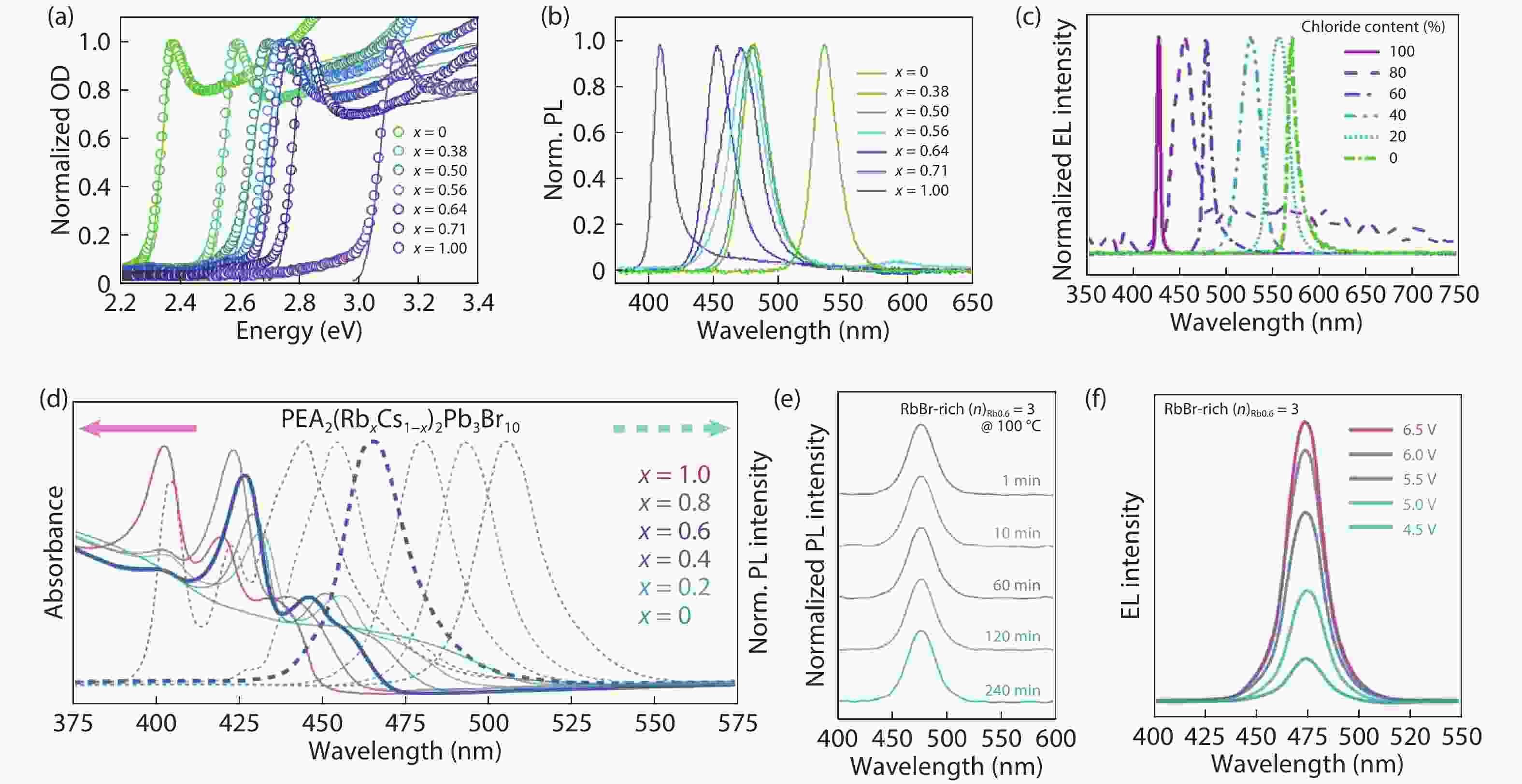
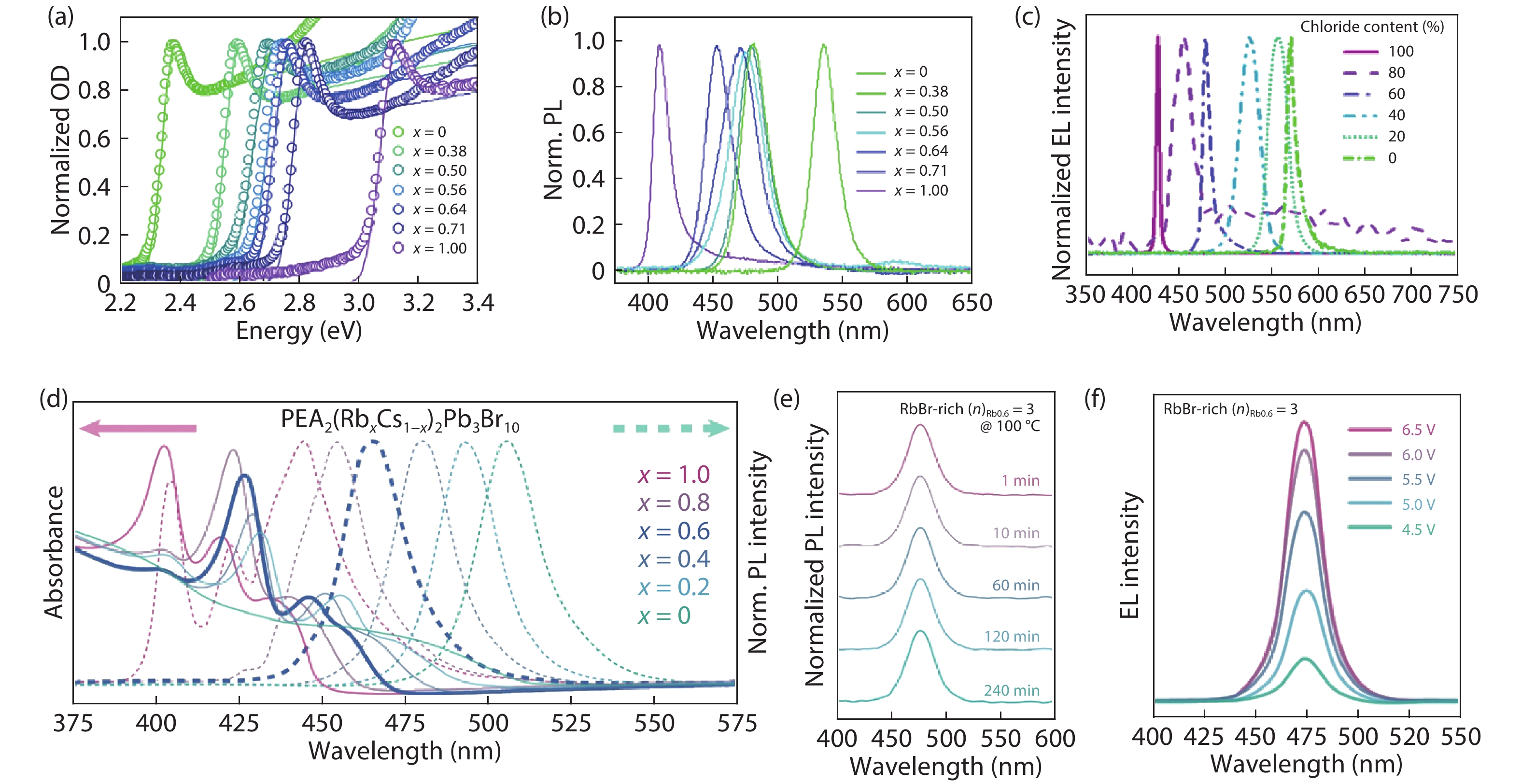
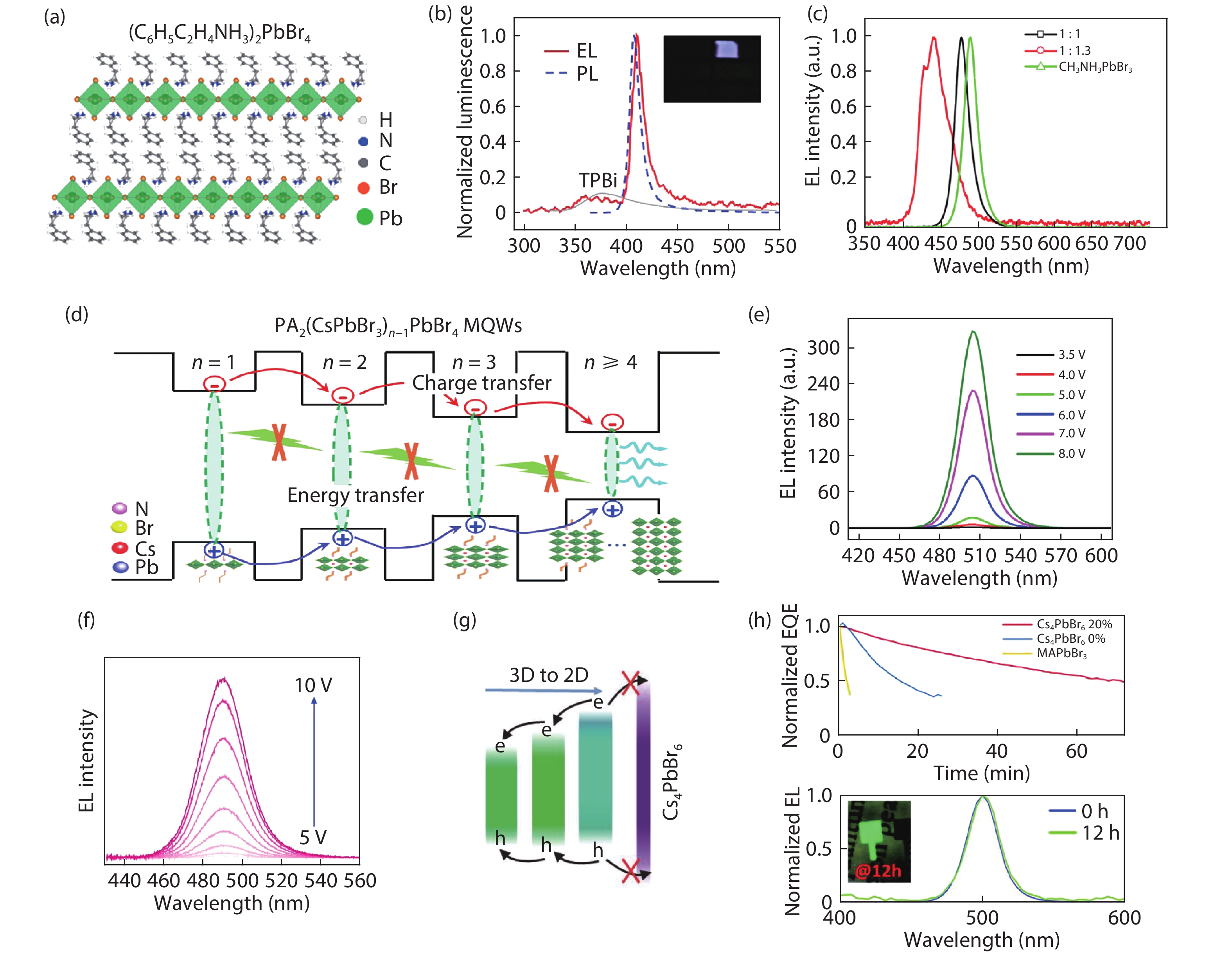
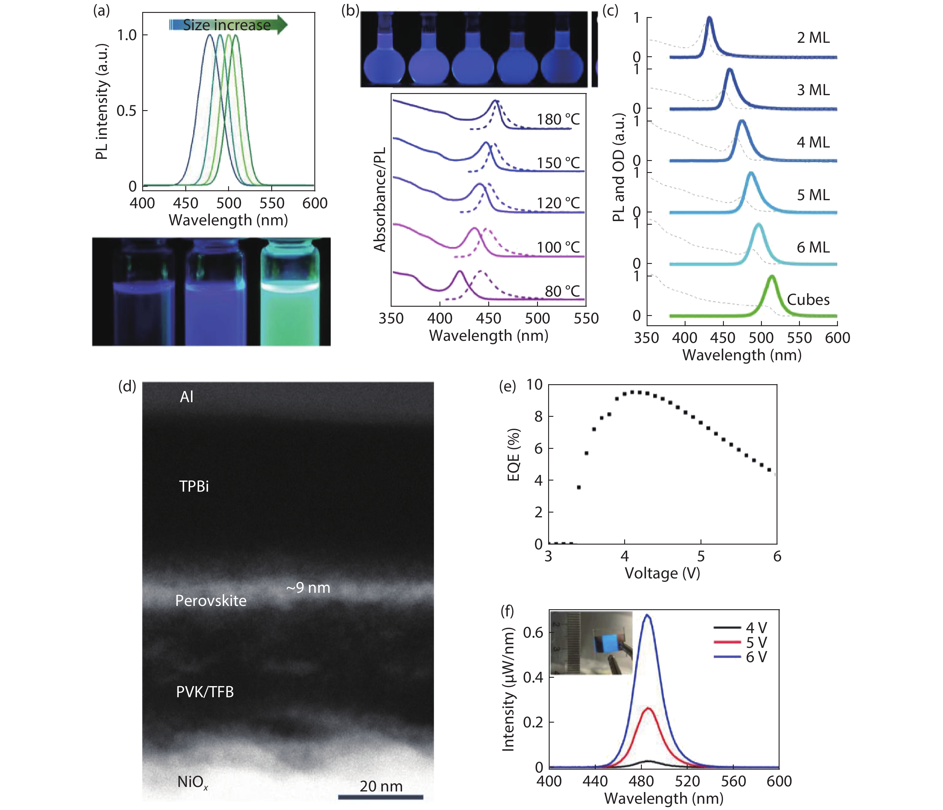
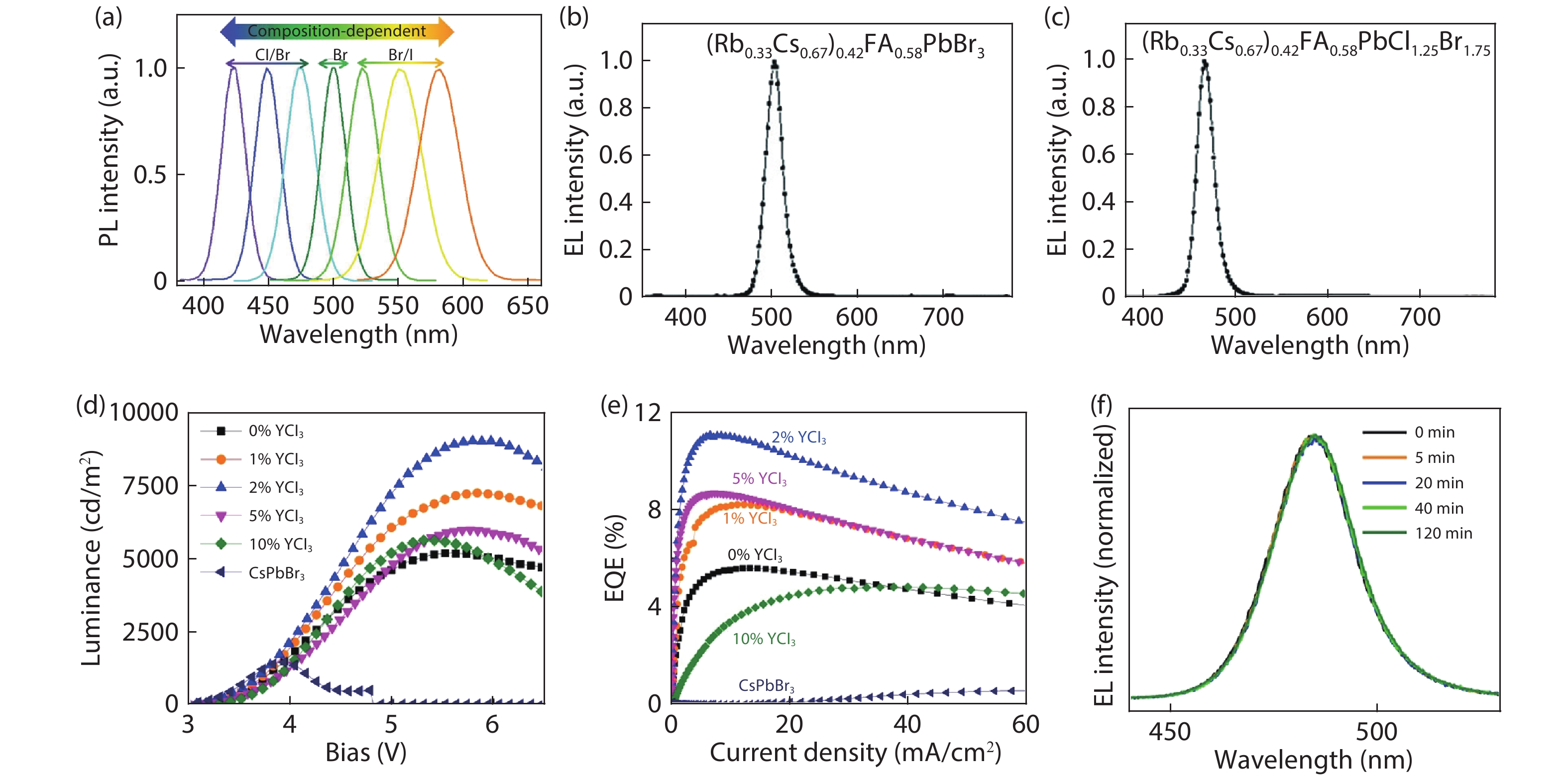
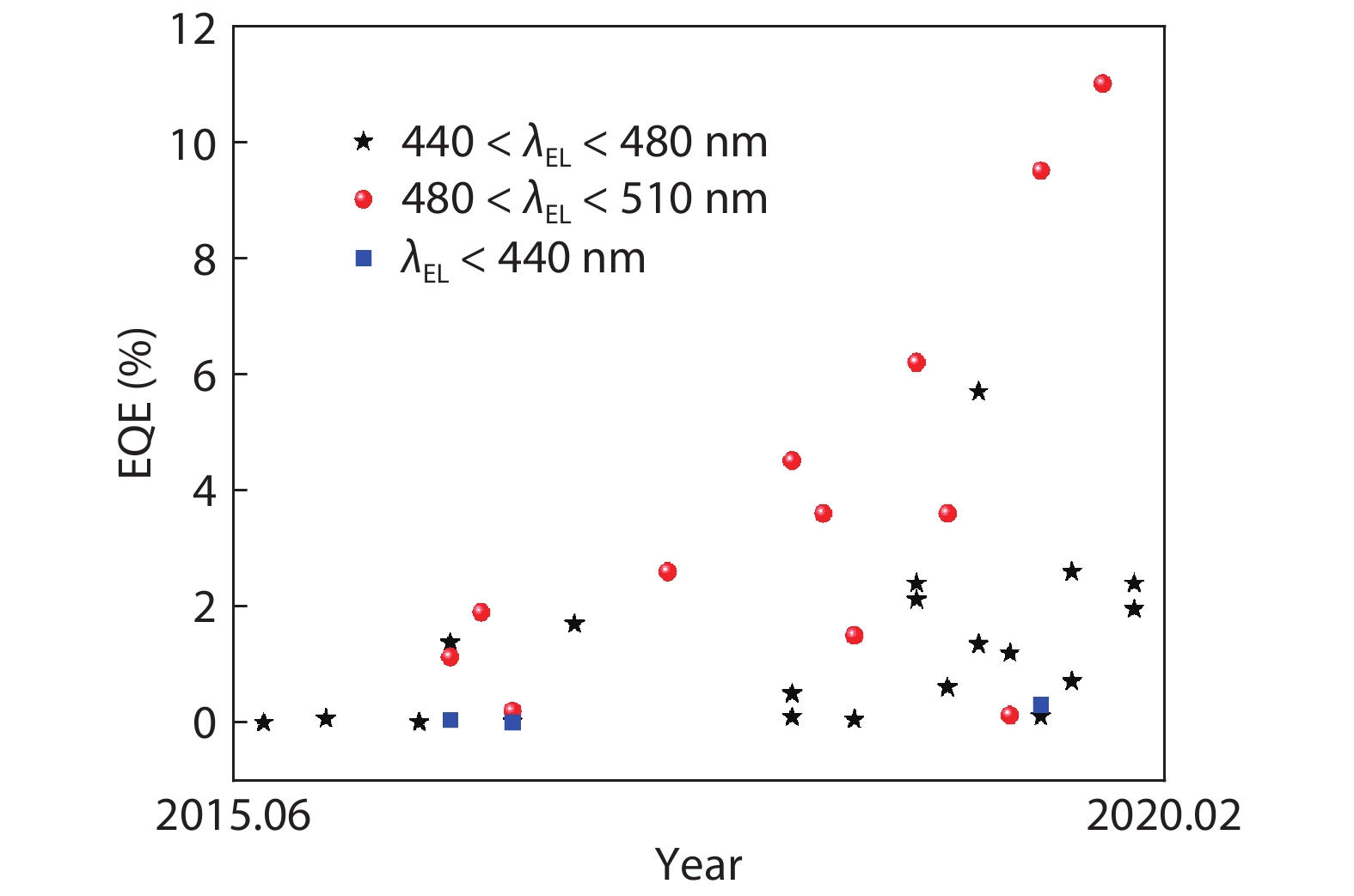
Metal halide perovskites have attracted tremendous interest due to their excellent optical and electrical properties, and they find many promising applications in the optoelectronic fields of solar cells, light-emitting diodes, and photodetectors. Thanks to the contributions of international researchers, significant progress has been made for perovskite light-emitting diodes (Pero-LEDs). The external quantum efficiencies (EQEs) of Pero-LEDs with emission of green, red, and near-infrared have all exceeded 20%. However, the blue Pero-LEDs still lag due to the poor film quality and deficient device structure. Herein, we summarize the strategies for preparing blue-emitting perovskites and categorize them into two: compositional engineering and size controlling of the emitting units. The advantages and disadvantages of both strategies are discussed, and a perspective of preparing high-performance blue-emitting perovskite is proposed. The challenges and future directions of blue Pero-LEDs fabrication are also discussed.
J. Semicond.
2020, 41(5): 051204 doi: 10.1088/1674-4926/41/5/051204
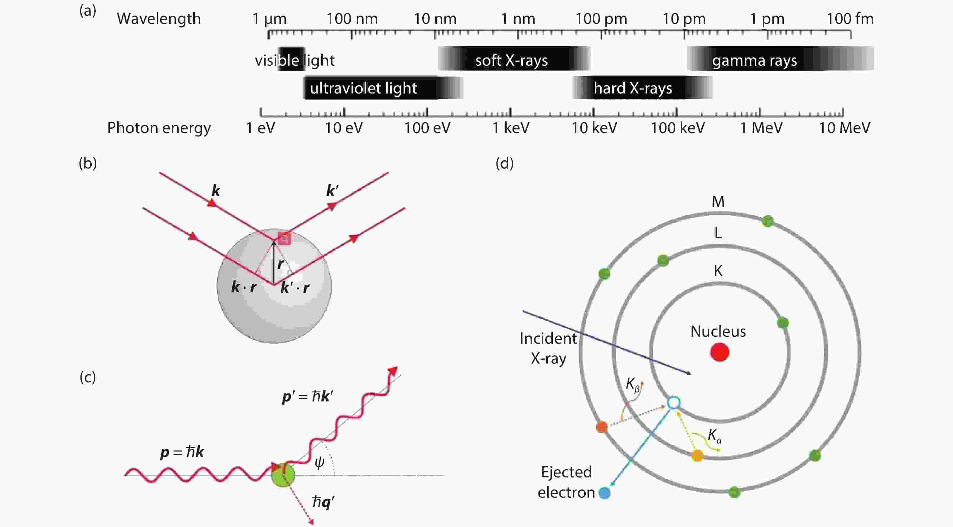
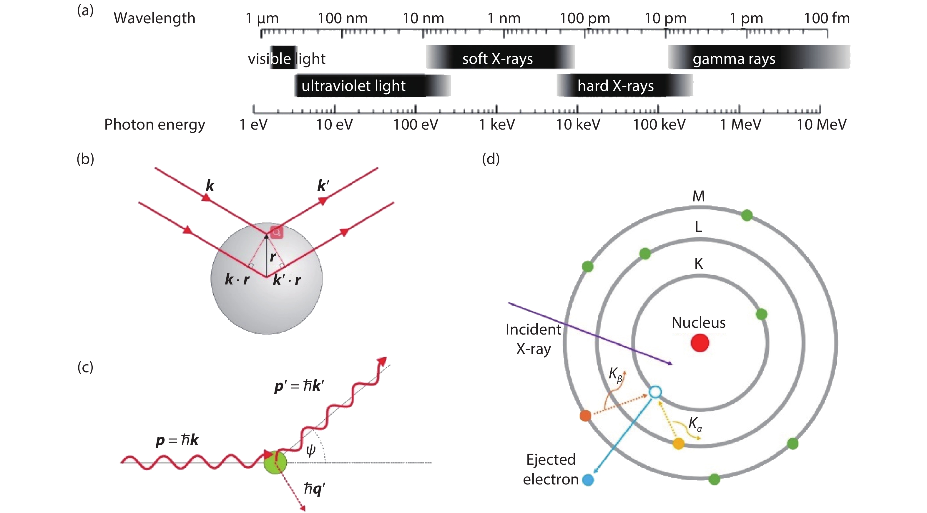
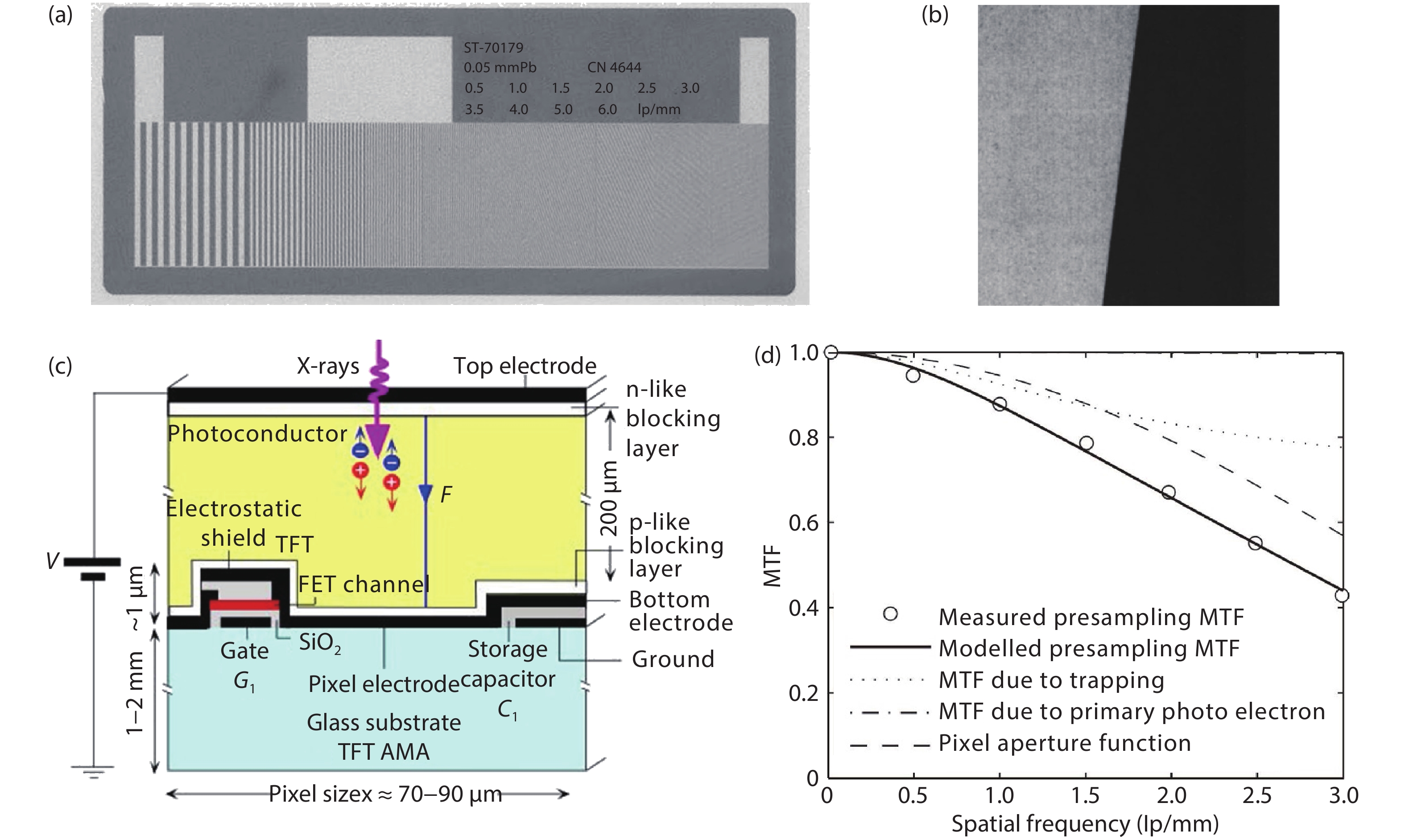
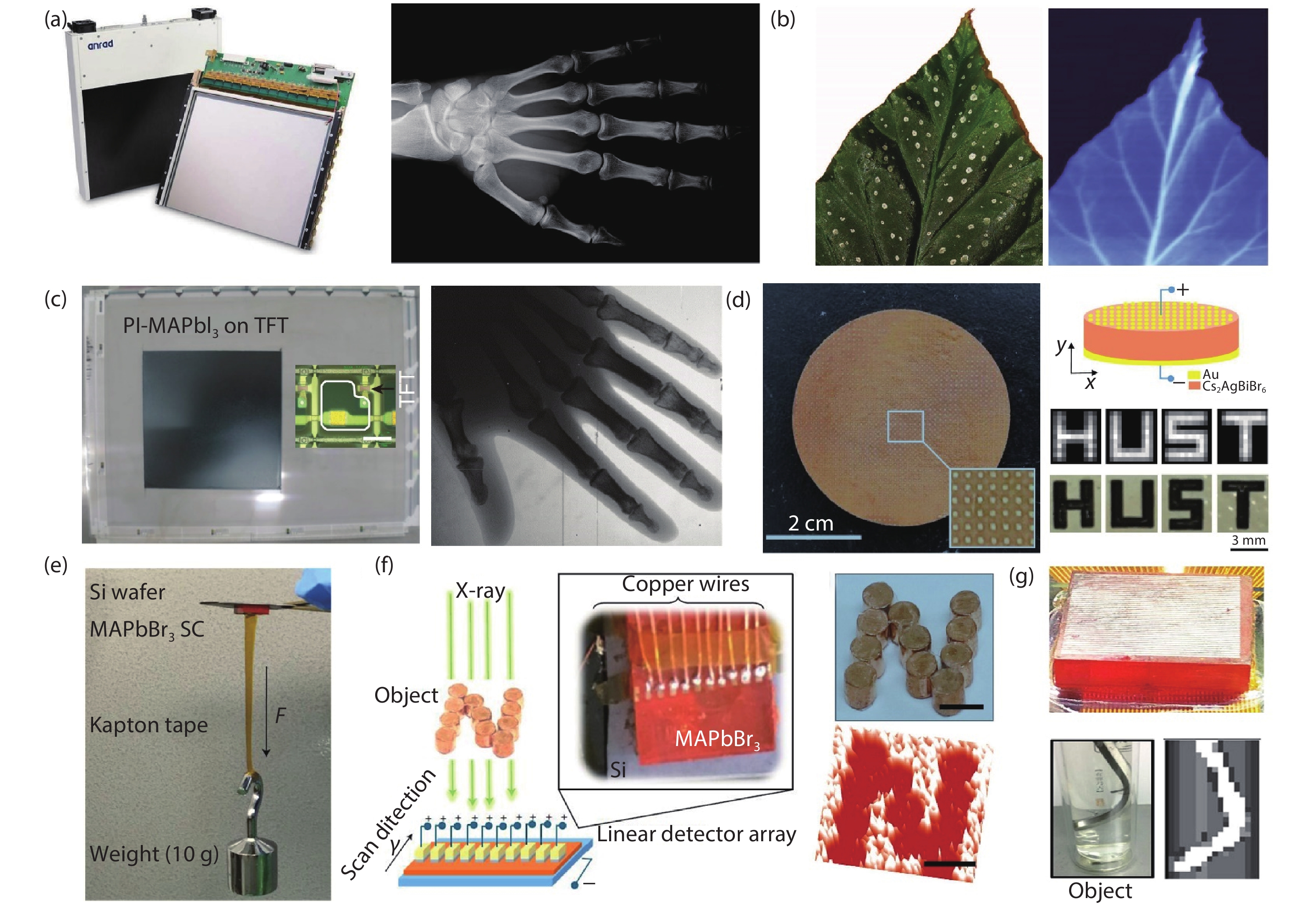
Halide perovskites have emerged as the next generation of optoelectronic materials and their remarkable performances have been attractive in the fields of solar cells, light-emitting diodes, photodetectors, etc. In addition, halide perovskites have been reported as an attractive new class of X-ray direct detecting materials recently, owning to the strong X-ray stopping capacity, excellent carrier transport, high sensitivity, and cost-effective manufacturing. Meanwhile, perovskite based direct X-ray imagers have been successfully demonstrated as well. In this review article, we firstly introduced some fundamental principles of direct X-ray detection and imaging, and summarized the advances of perovskite materials for these purposes and finally put forward some needful and feasible directions.

J. Semicond.
2020, 41(5): 051205 doi: 10.1088/1674-4926/41/5/051205

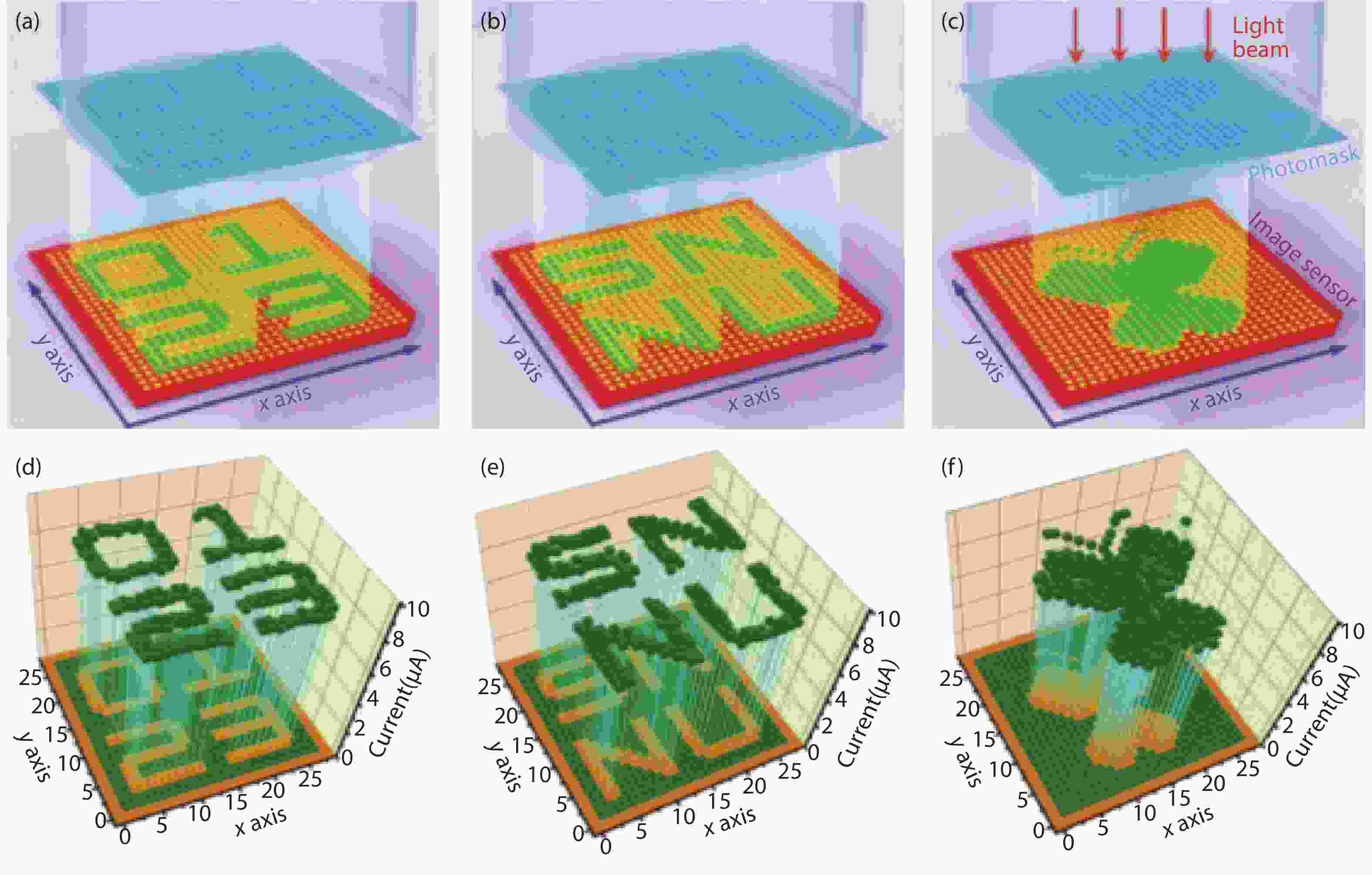
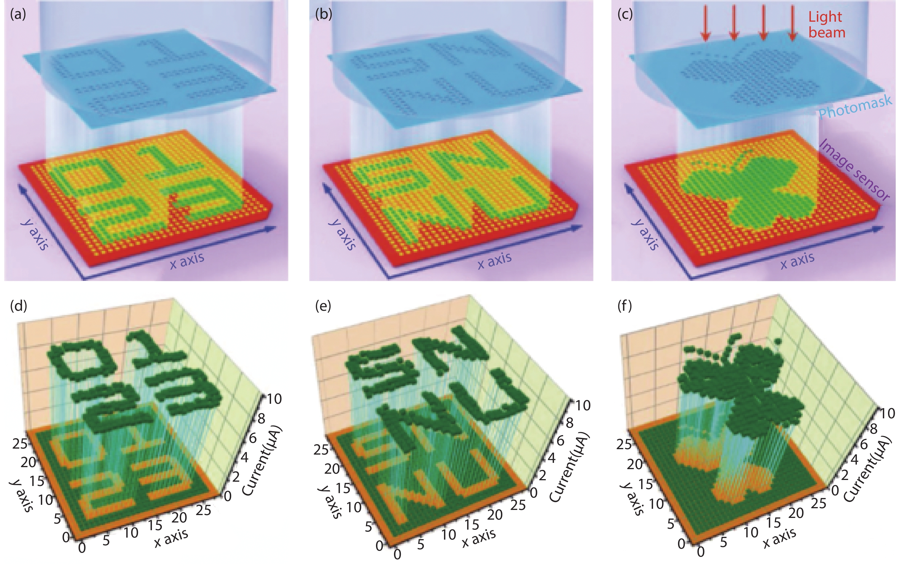
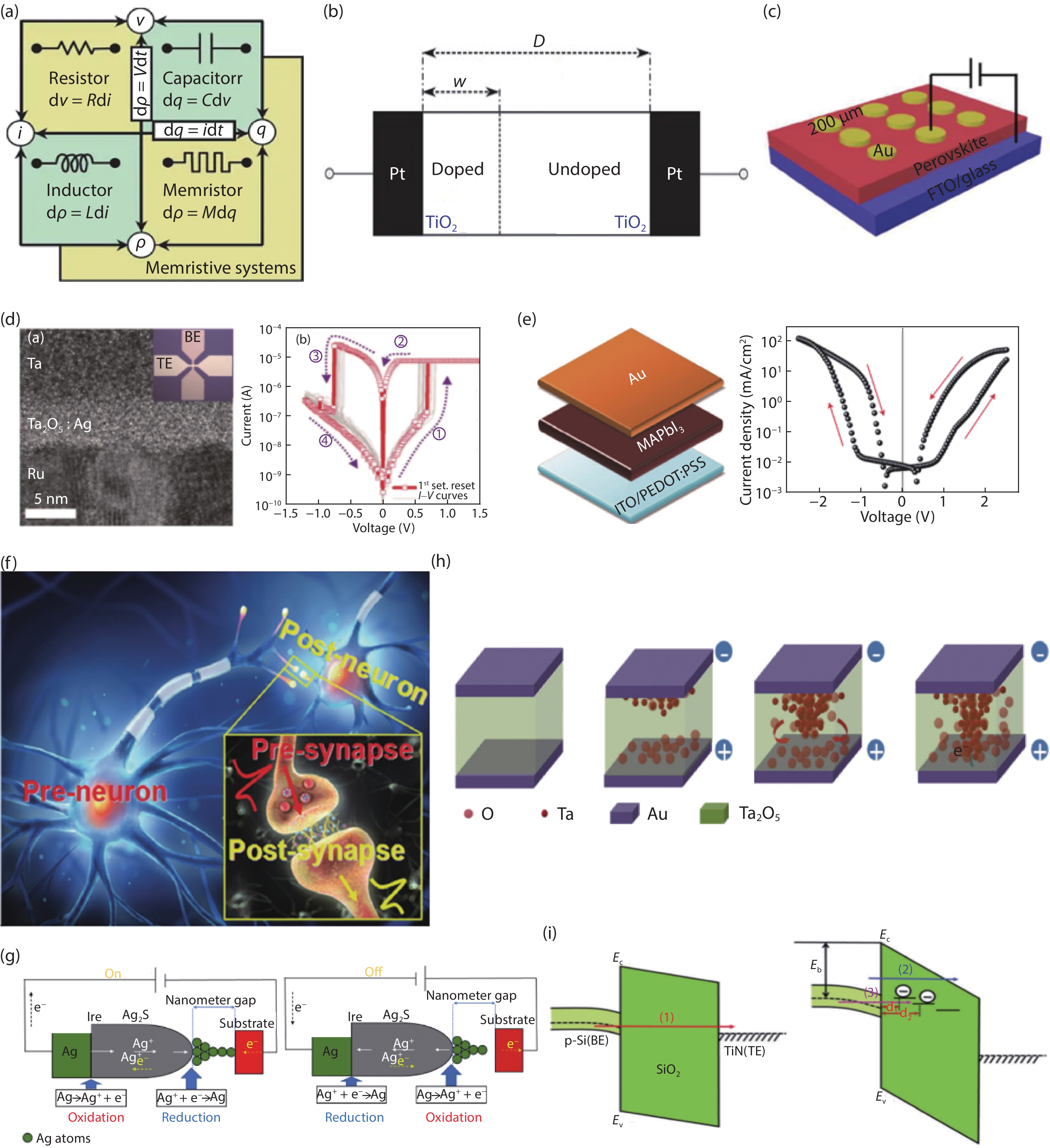
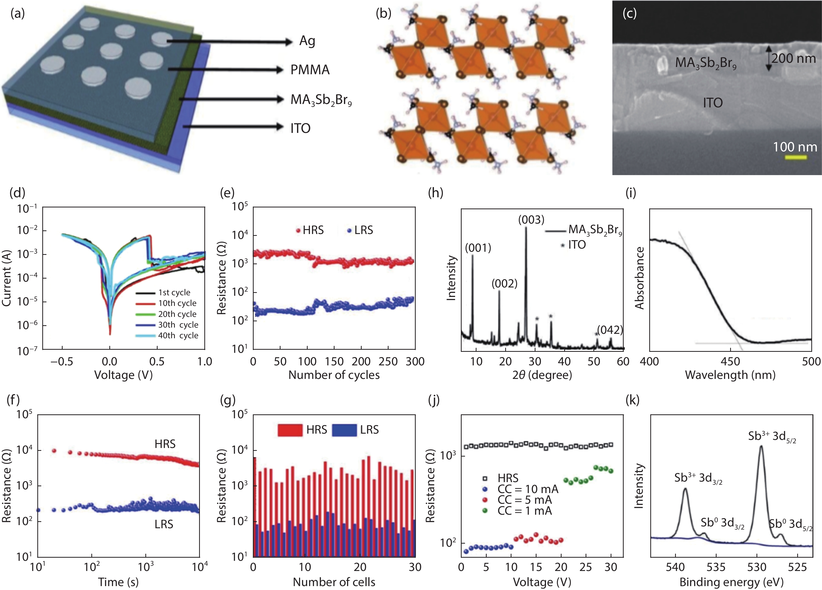
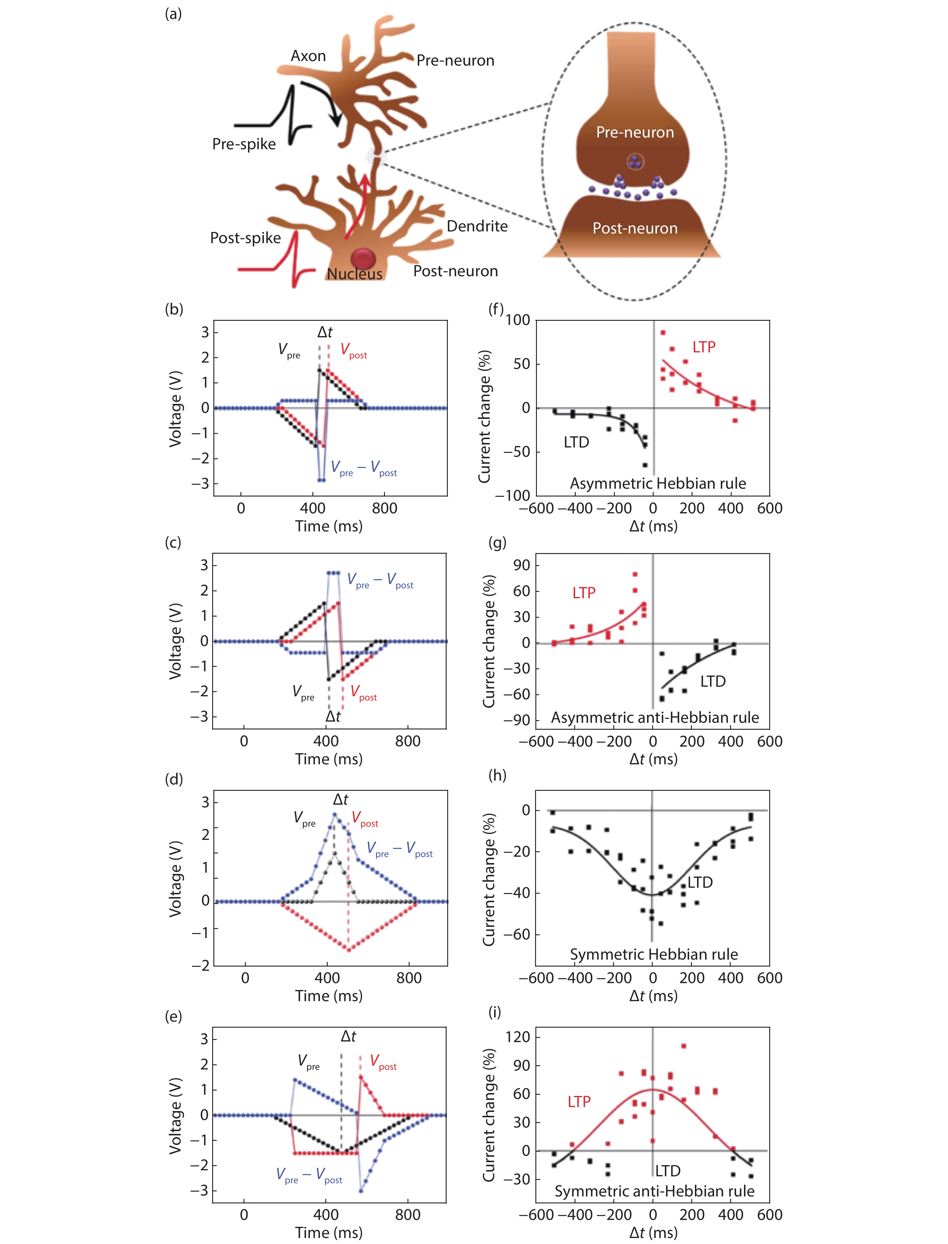
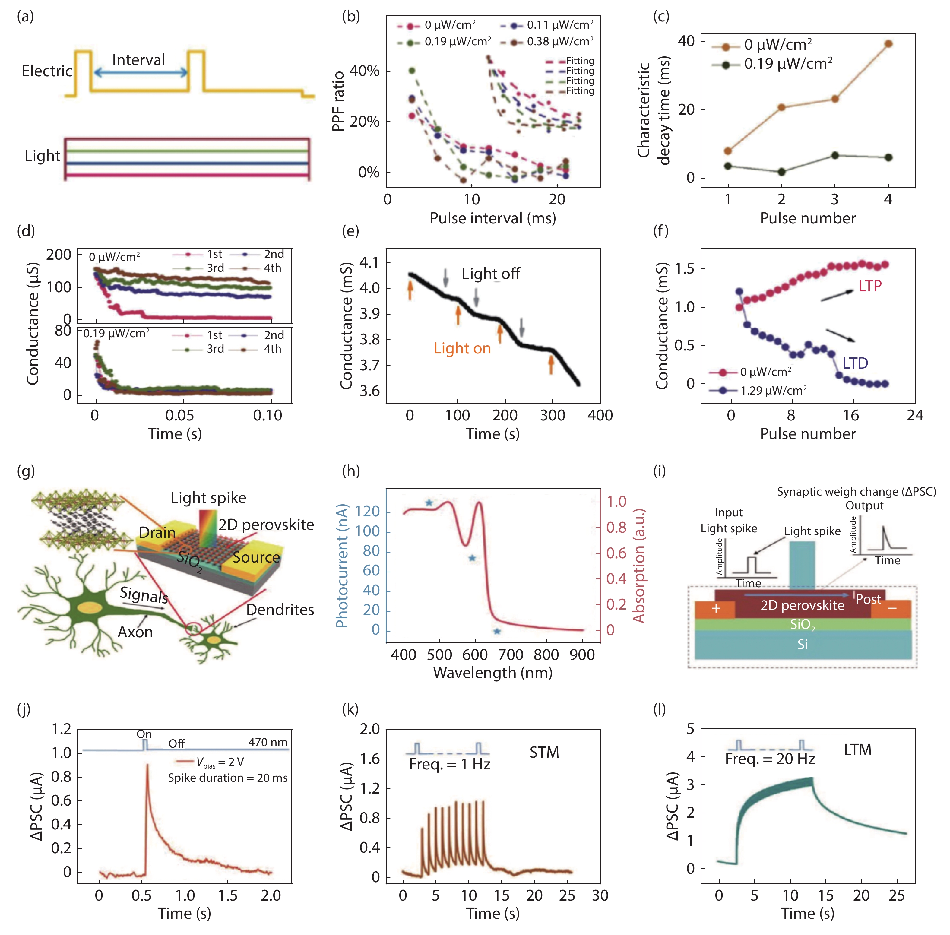
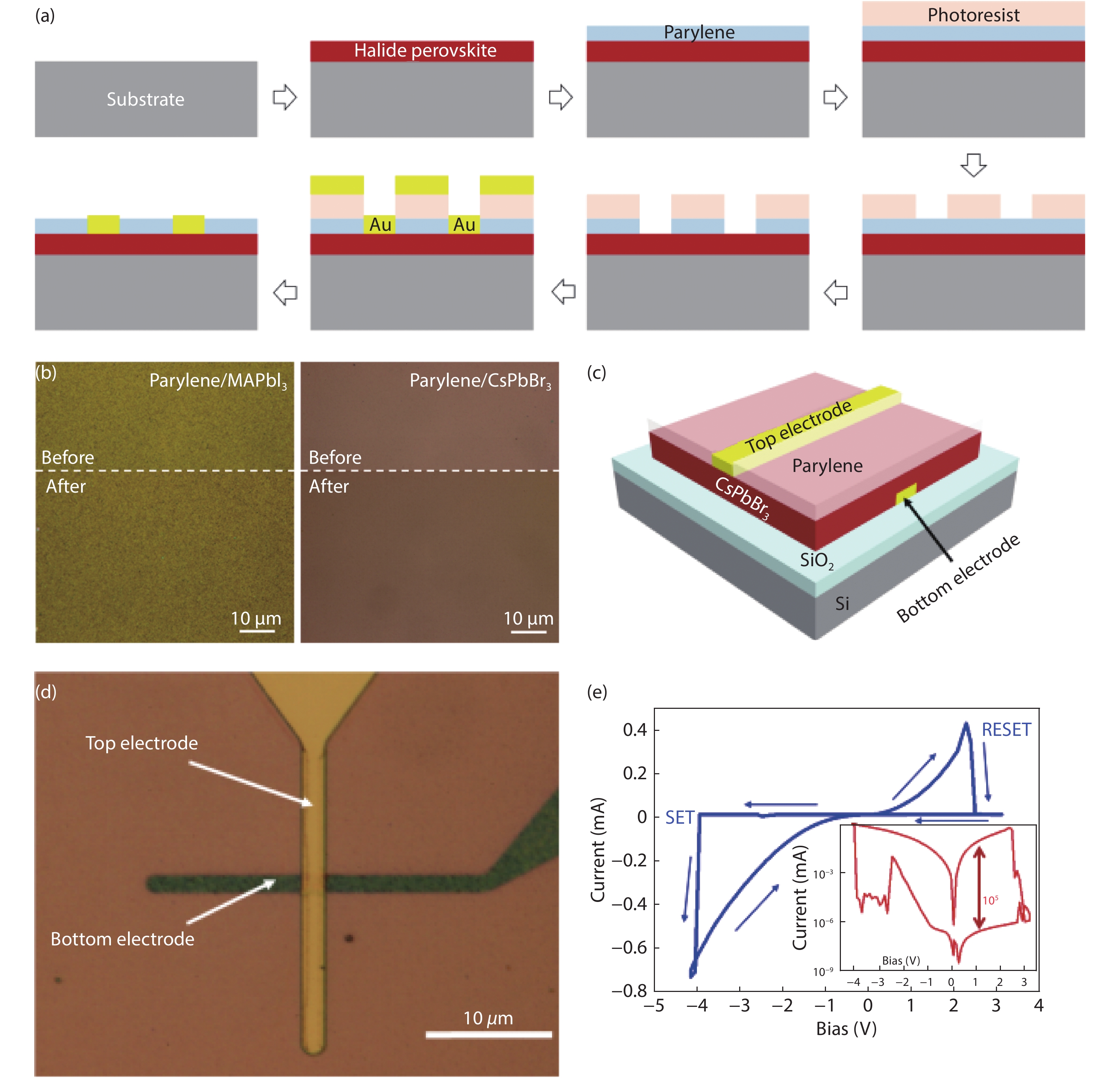
New neuromorphic architectures and memory technologies with low power consumption, scalability and high-speed are in the spotlight due to the von Neumann bottleneck and limitations of Moore's law. The memristor, a two-terminal synaptic device, shows powerful capabilities in neuromorphic computing and information storage applications. Active materials with high defect migration speed and low defect migration barrier are highly promising for high-performance memristors. Halide perovskite (HP) materials with point defects (such as gaps, vacancies, and inversions) have strong application potential in memristors. In this article, we review recent advances on HP memristors with exceptional performances. First, the working mechanisms of memristors are described. Then, the structures and properties of HPs are explained. Both electrical and photonic HP-based memristors are overviewed and discussed. Different fabrication methods of HP memristor devices and arrays are described and compared. Finally, the challenges in integrating HP memristors with complementary metal oxide semiconductors (CMOS) are briefly discussed. This review can assist in developing HP memristors for the next-generation information technology.


J. Semicond.
2020, 41(5): 052201 doi: 10.1088/1674-4926/41/5/052201
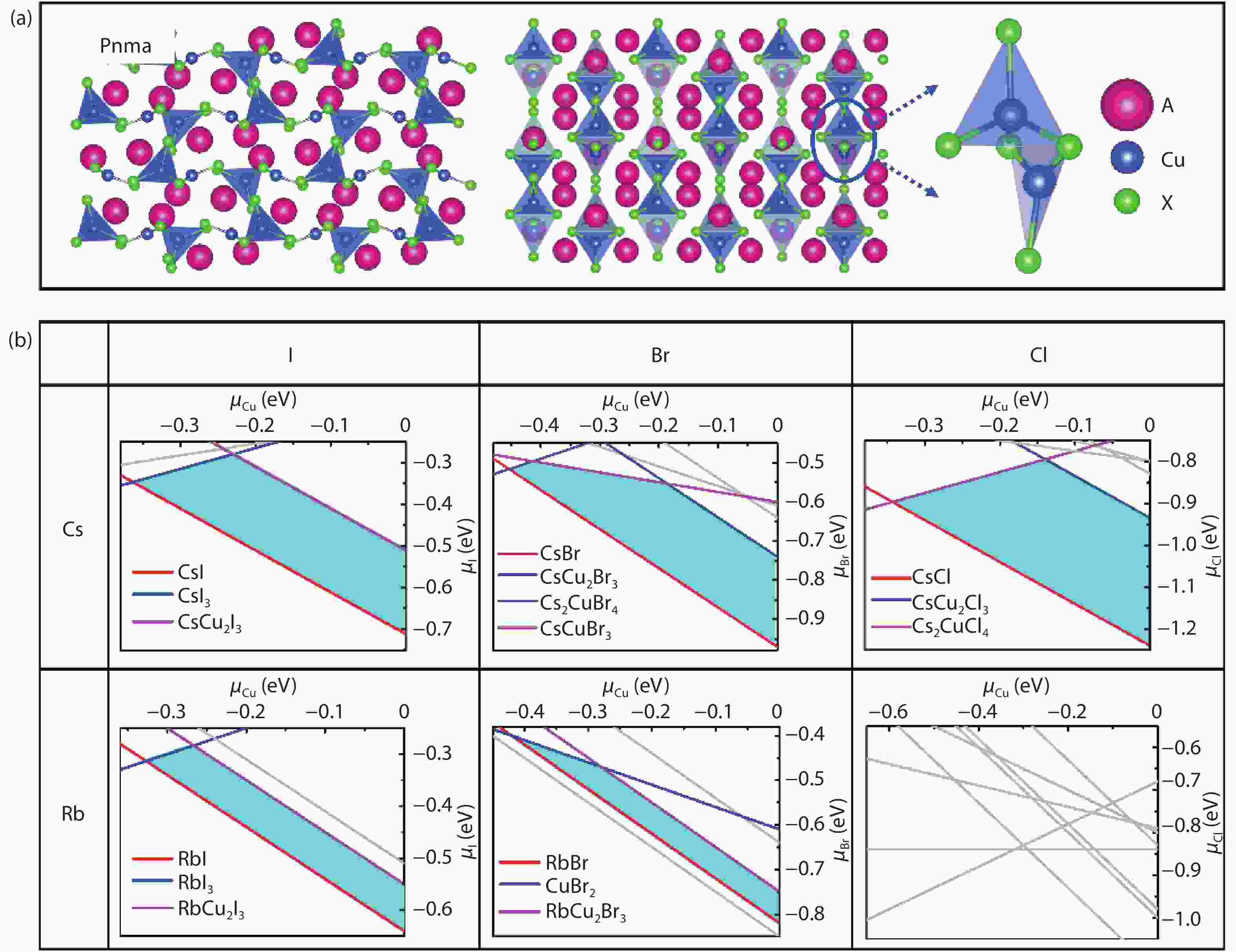
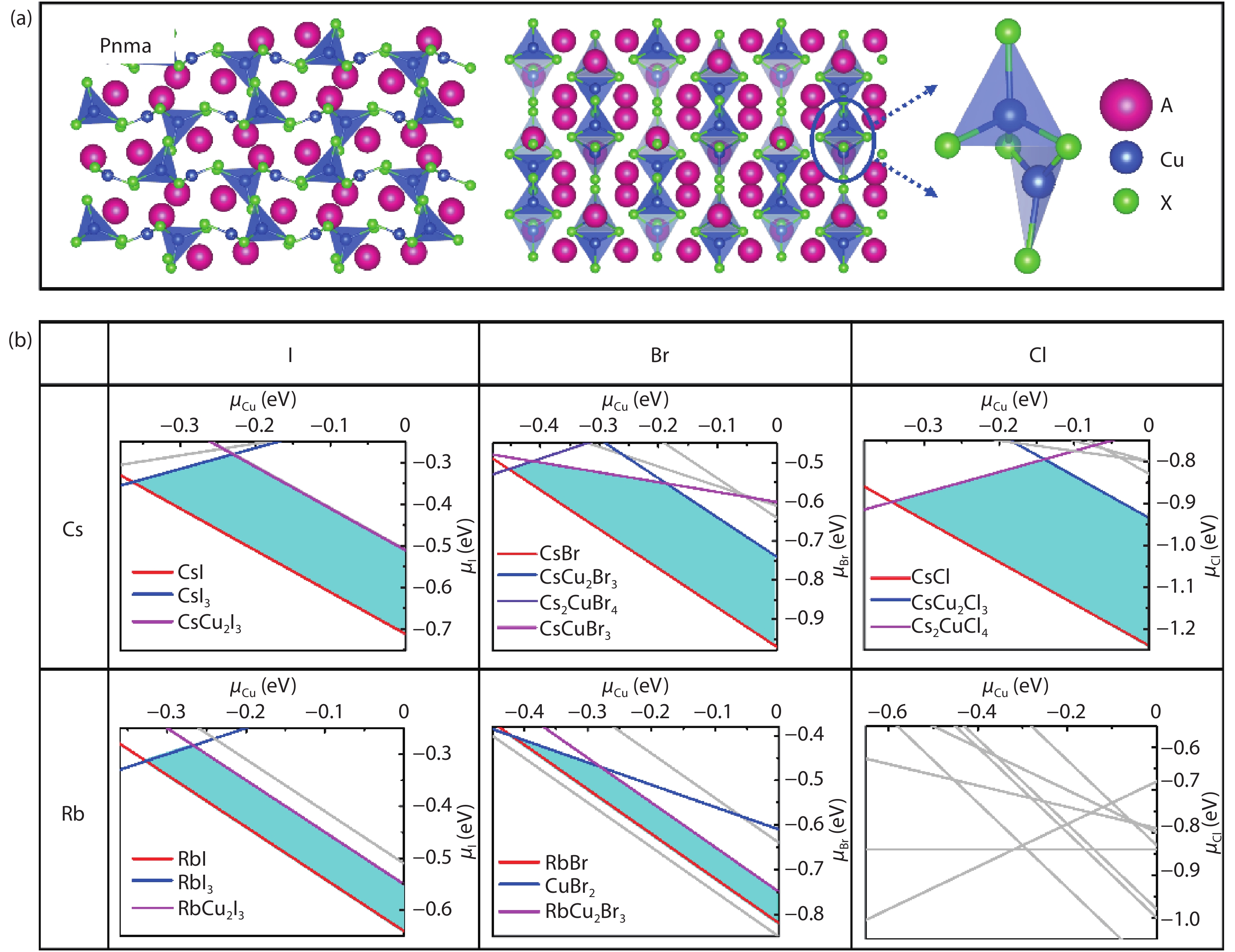
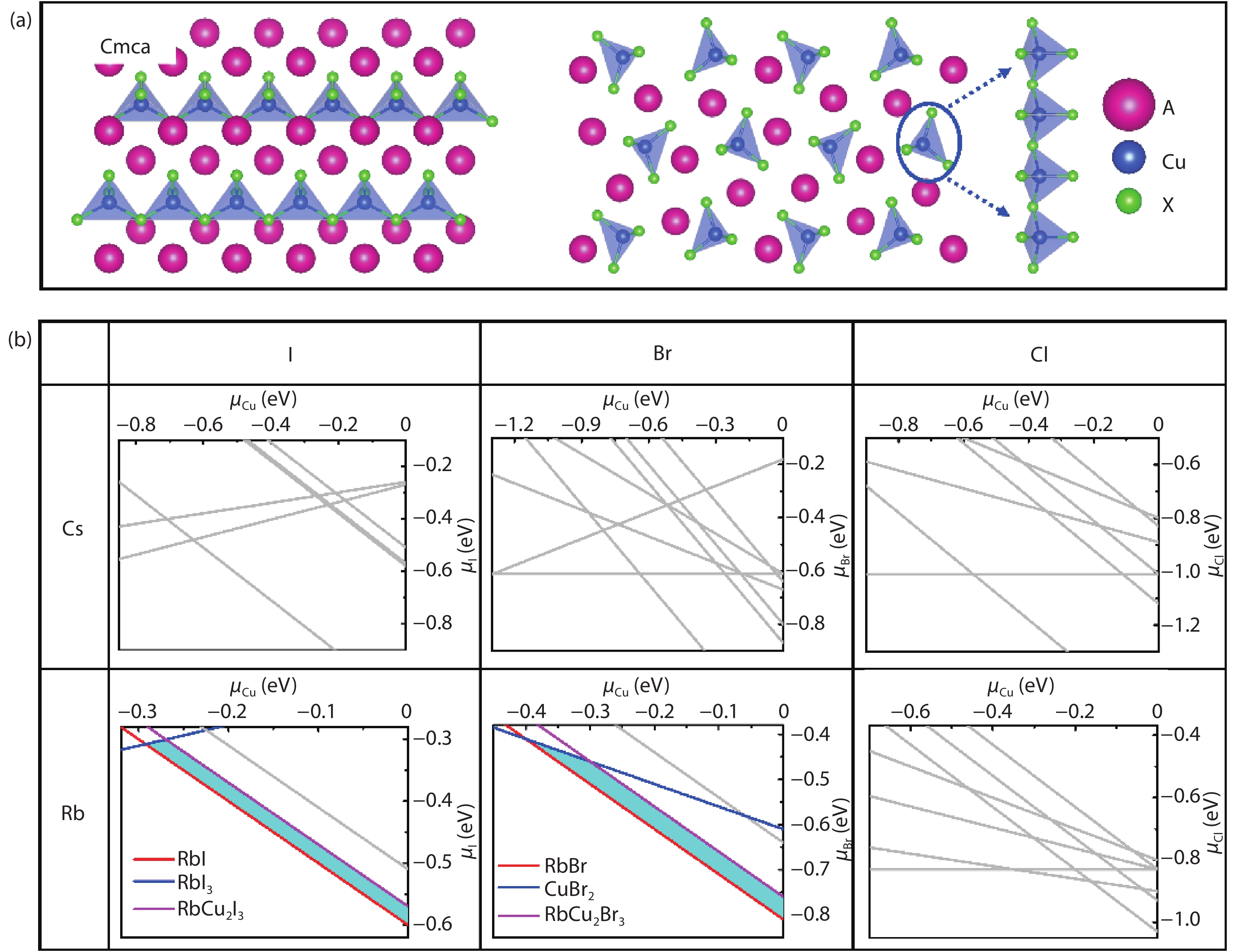
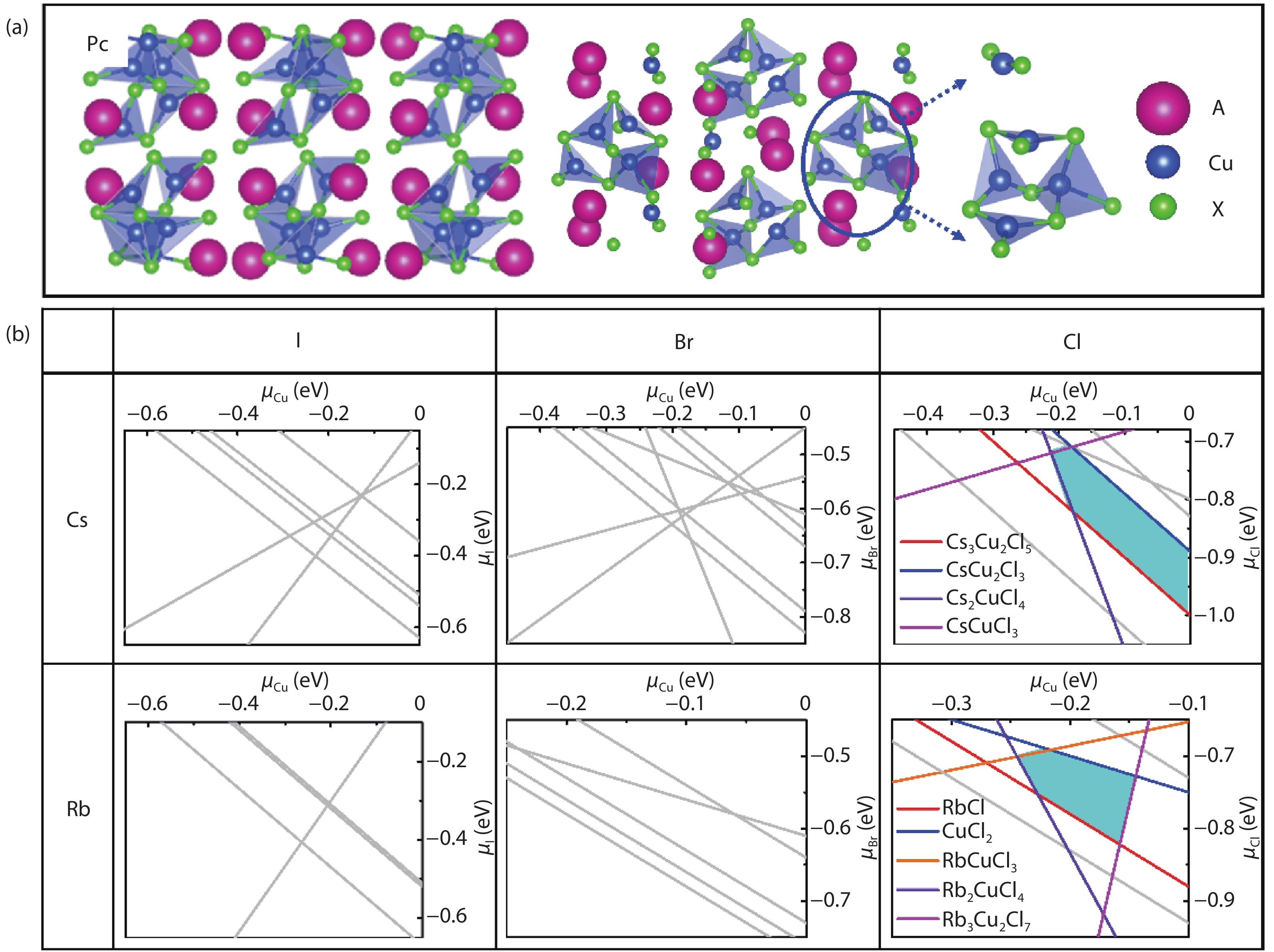
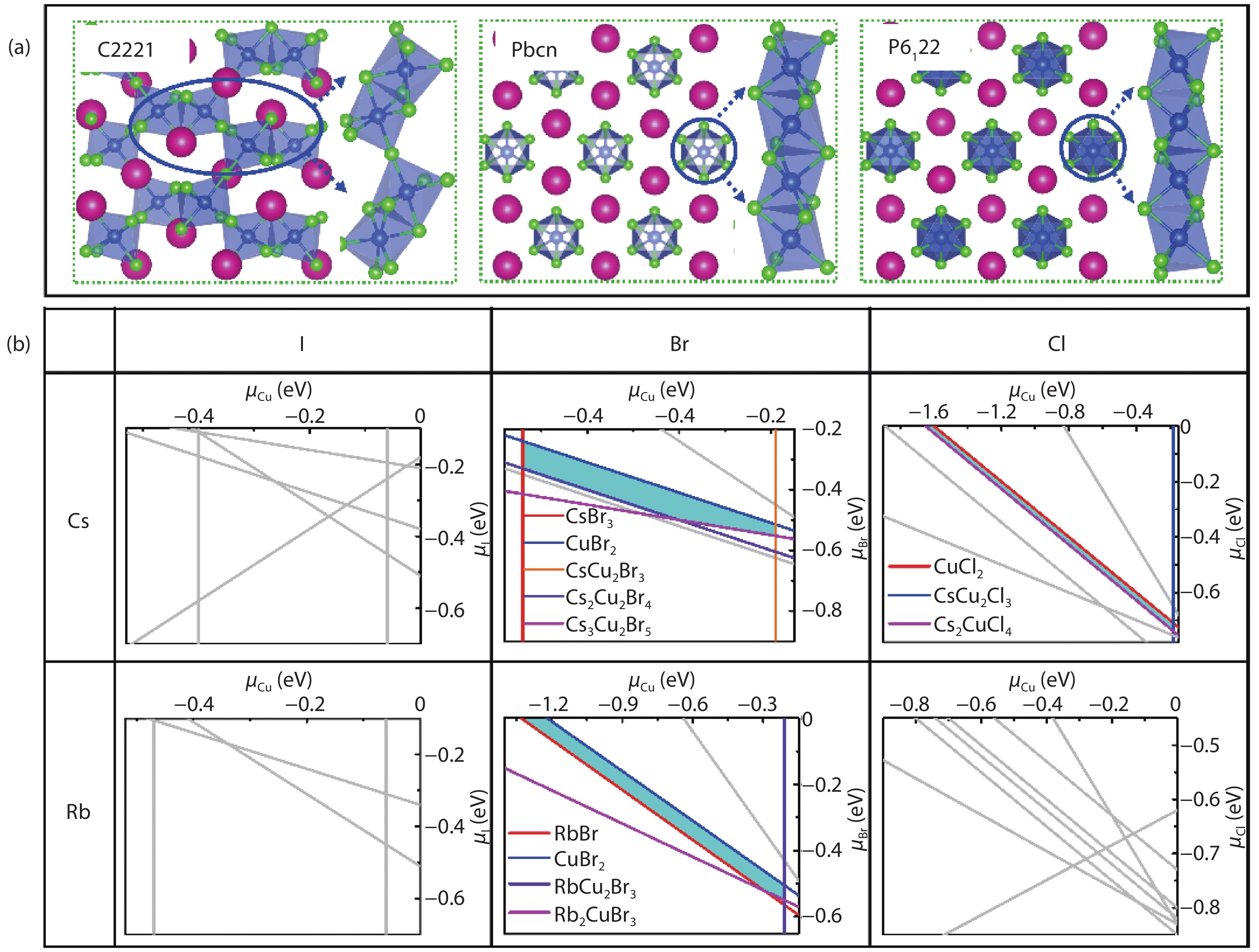
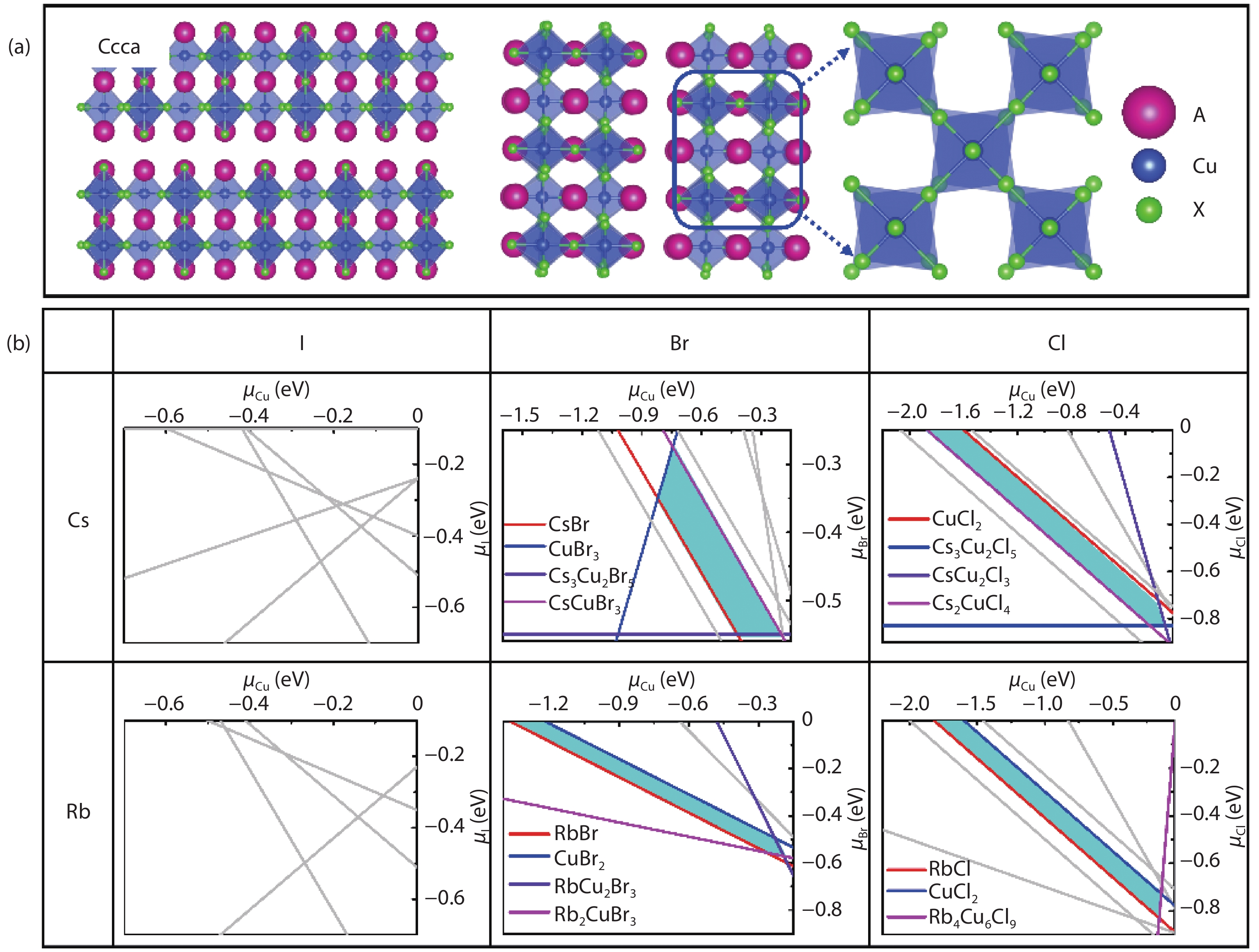
Recently, inorganic copper-based halide perovskites and their derivatives (CHPs) with chemical formulas AlCumXn (A = Rb and Cs; X = Cl, Br and I; l, m, and n are integers.), have received increasing attention in the photoluminescence field, due to their lead-free, cost-effective, earth-abundant and low electronic dimensionality. Ascribed to flexible valence charge of Cu (Cu1+ and Cu2+) and complex competing phases, the crystal structures and phase stabilities of CHPs are complicated and ambiguous, which limits their experimental applications. Via comprehensive first-principles calculations, we have investigated thermodynamic stabilities of possible crystal phases for AlCumXn by considering all the possible secondary phases existing in inorganic crystal structure database (ICSD). Our results are in agreement with existing experiments and further predicted the existence of 10 stable CHPs, i.e. Rb3Cu2Br5, Rb3Cu2I5, RbCu2Cl3, Rb2CuI3, Rb2CuBr4, RbCuBr3, Rb3Cu2Br7, Cs3Cu2Br7, Cs3Cu2Cl7 and Cs4Cu5Cl9, which have not yet been reported in experiments. This work provides a phase and compositional map that may guide experiments to synthesize more novel inorganic CHPs with diverse properties for potential functional applications.


J. Semicond.
2020, 41(5): 052202 doi: 10.1088/1674-4926/41/5/052202

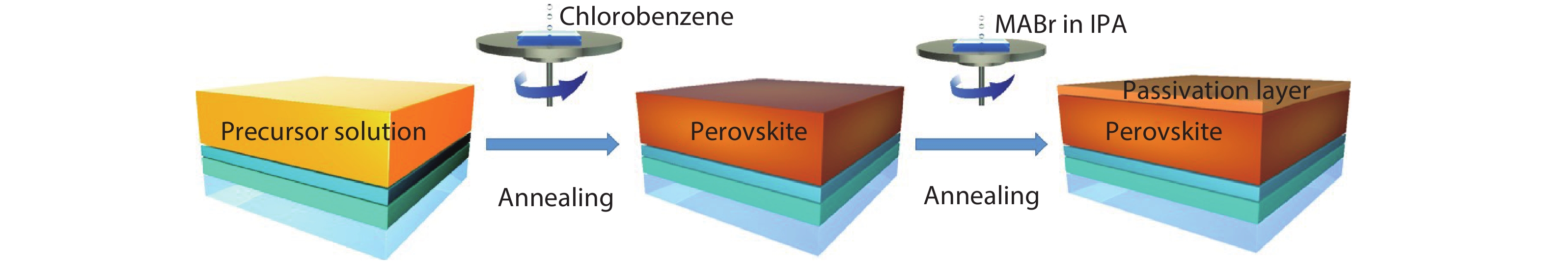
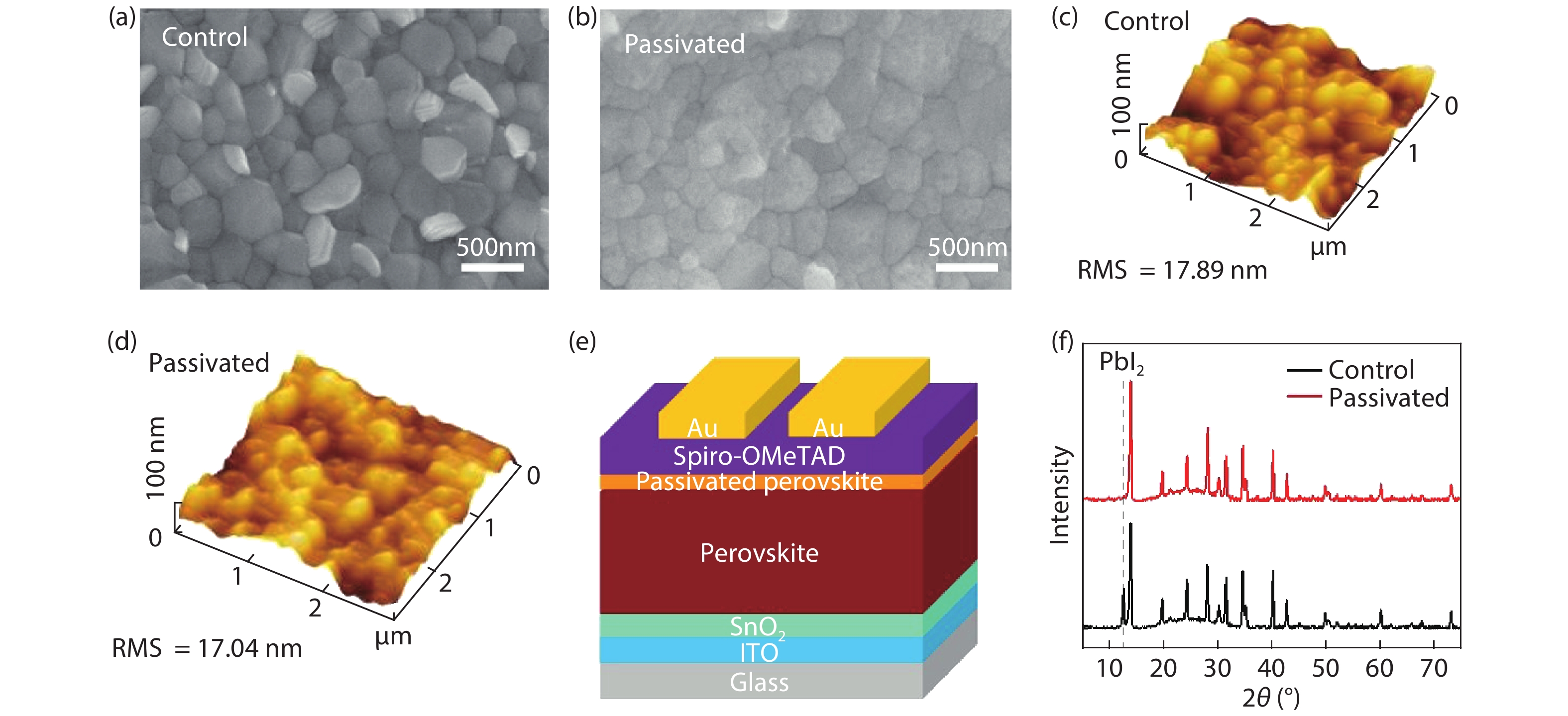
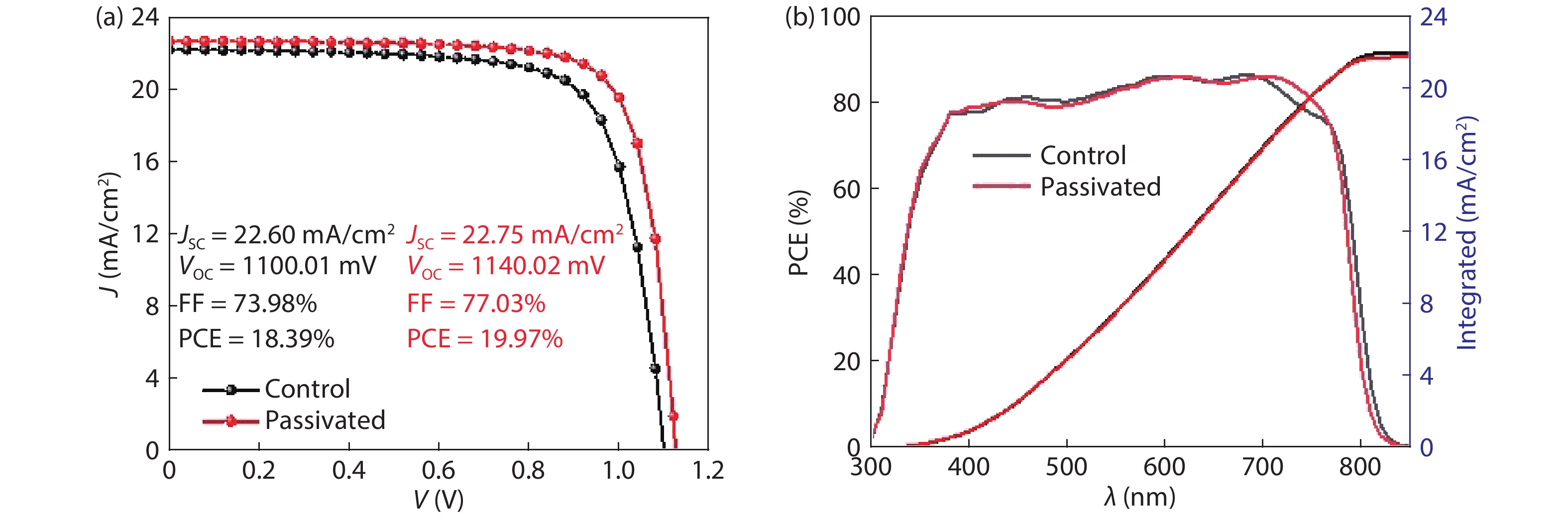
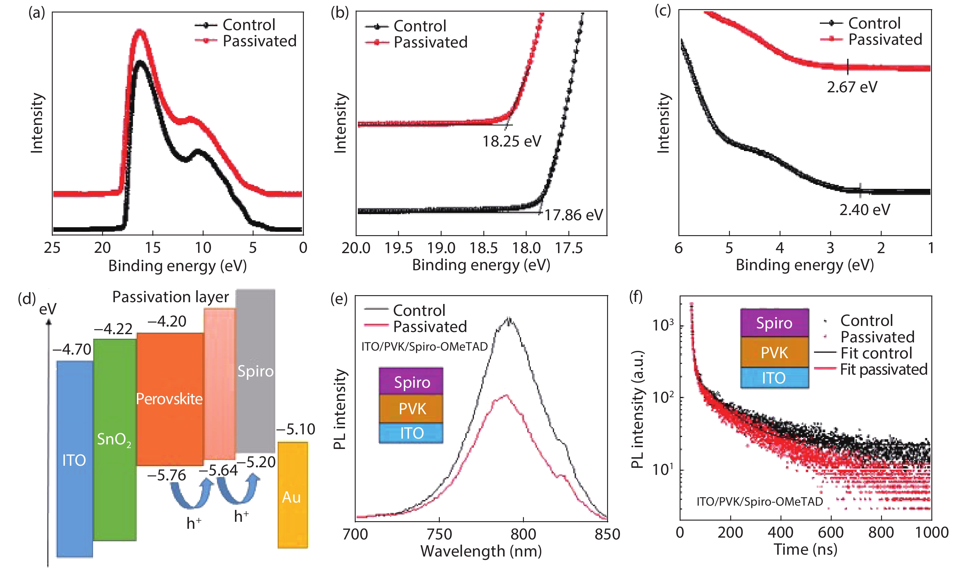
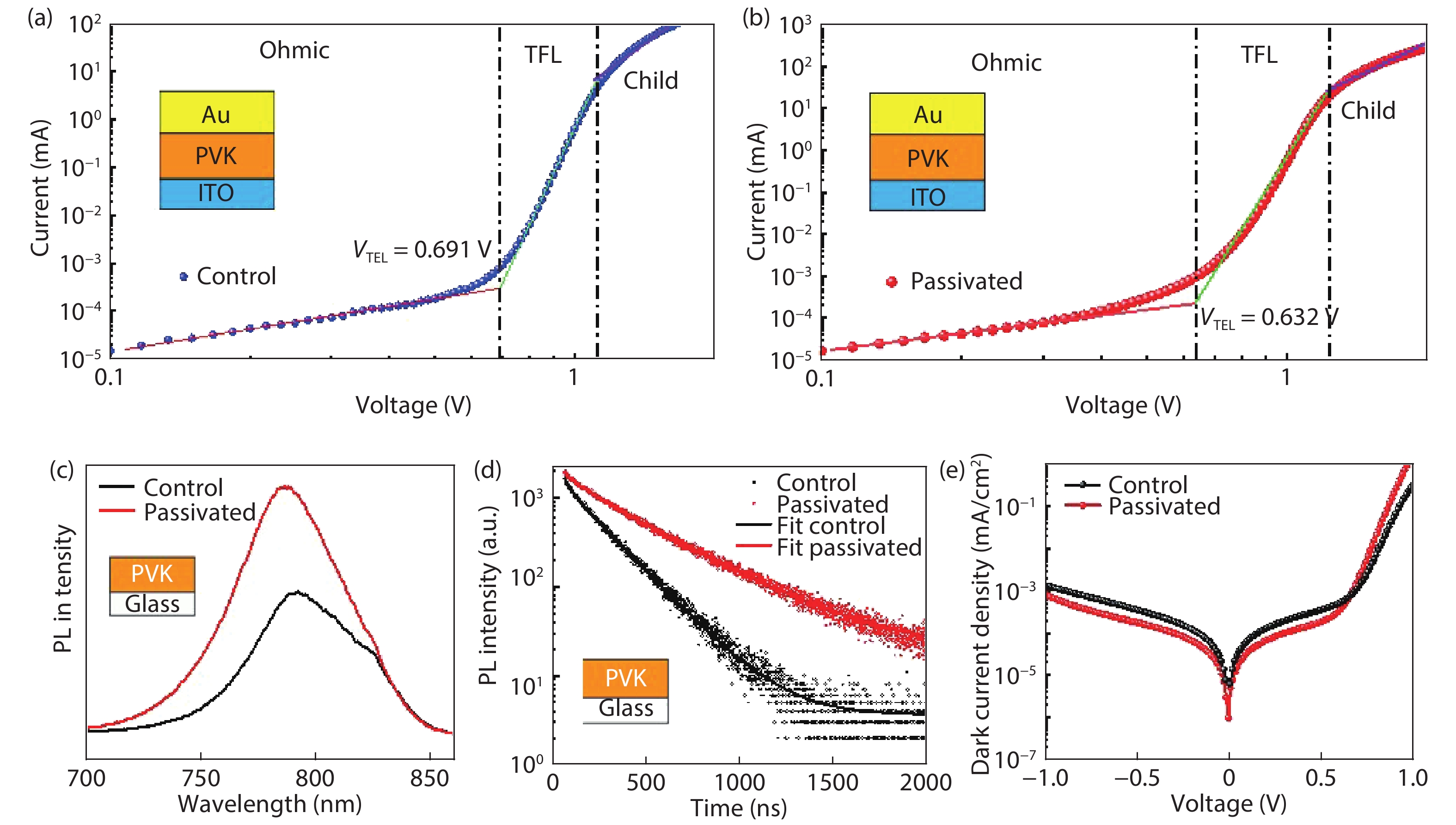
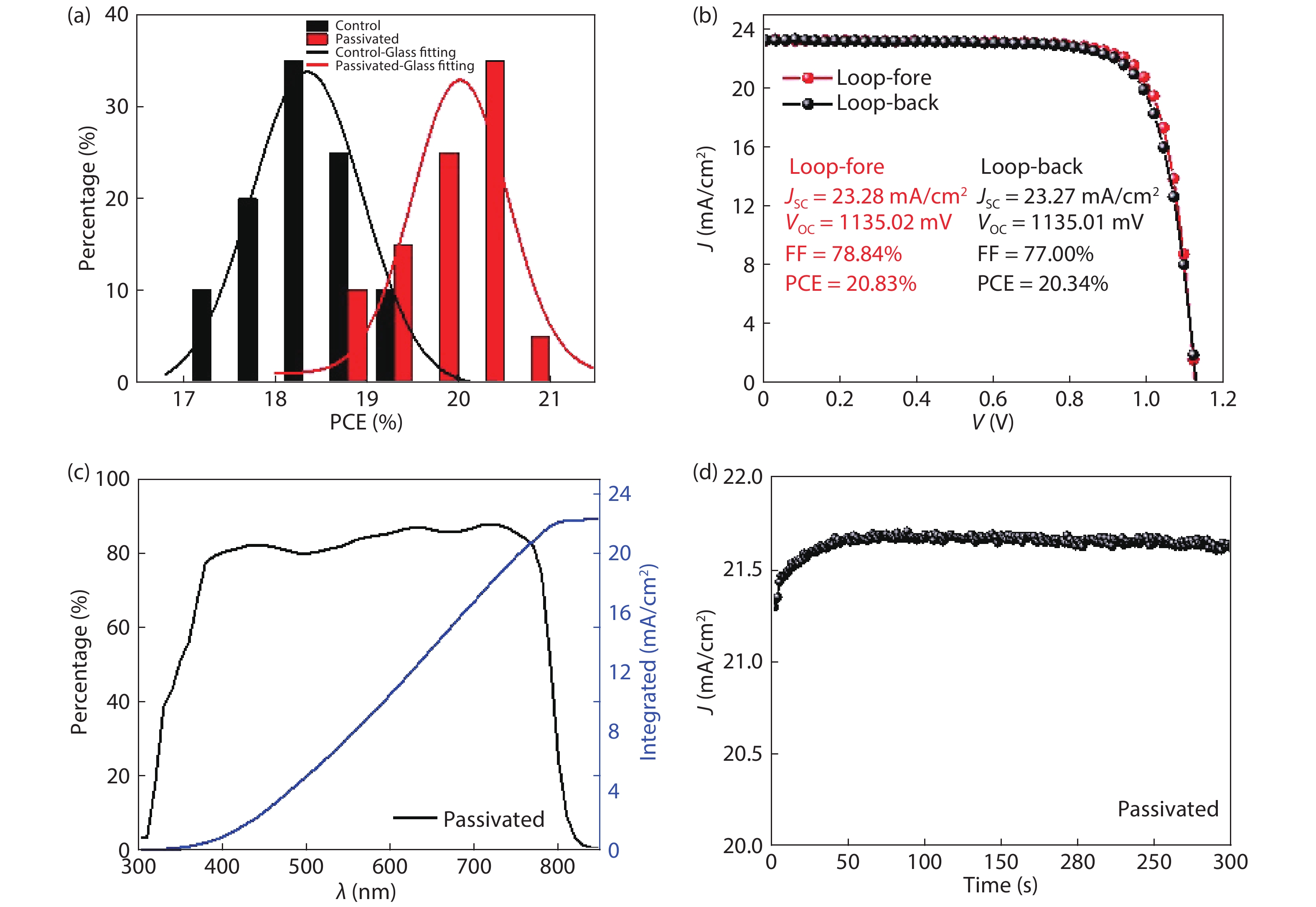
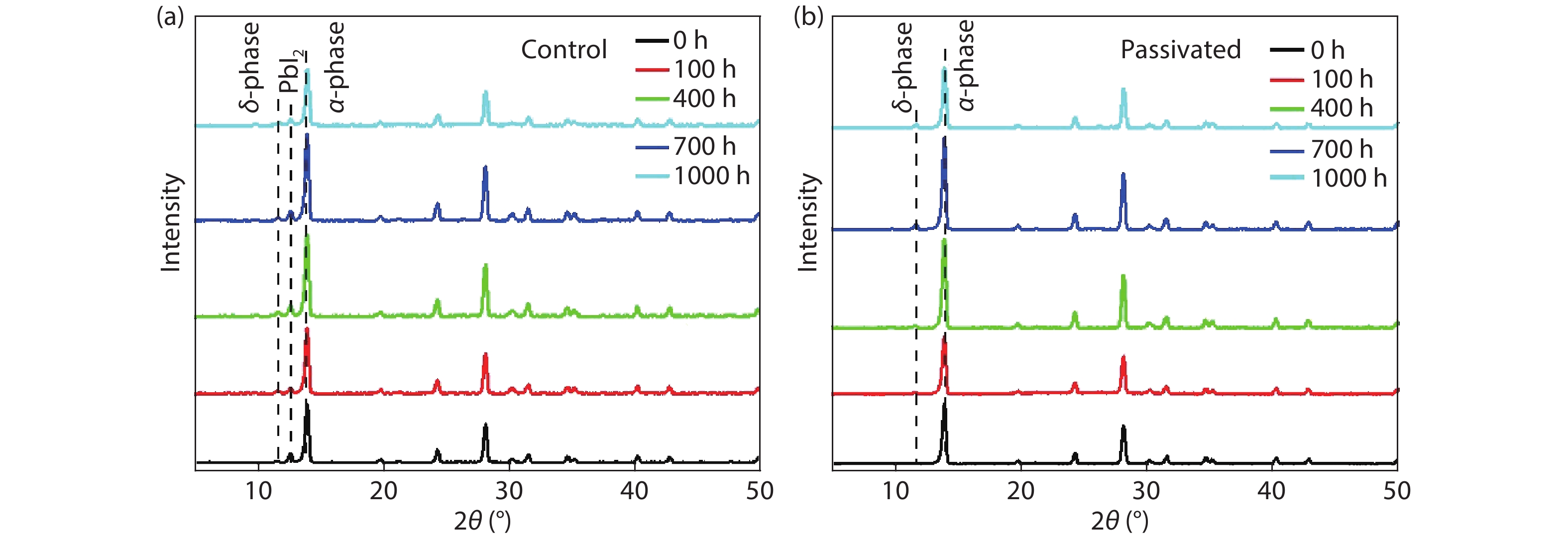
Interface engineering has played an increasingly essential role in the development of perovskite solar cells (PSCs). Herein, we adopted an effective and simple one-step interface passivation method on a FA-based perovskite to fabricate efficient and stable planar PSCs. The surface defects are reduced by the perovskite interface passivation layer incorporated between the hole transport and perovskite absorber layers, and then non-radiative recombination is suppressed while interfacial carrier extraction is enhanced. The passivated planar PSCs demonstrates 20.83% power conversion efficiency (PCE), which is caused by the simultaneous enhancement of the fill factor and open-circuit voltage. In addition, the device also shows great ambient and thermal stability. It retains 94% of its original PCE after 1000 h under ambient air without encapsulation as well as 90% of its initial efficiency after 400 h under continuous heating at 65 °C with encapsulation. This research provides a strategy for the development of efficient and stable PSCs.

J. Semicond.
2020, 41(5): 052203 doi: 10.1088/1674-4926/41/5/052203
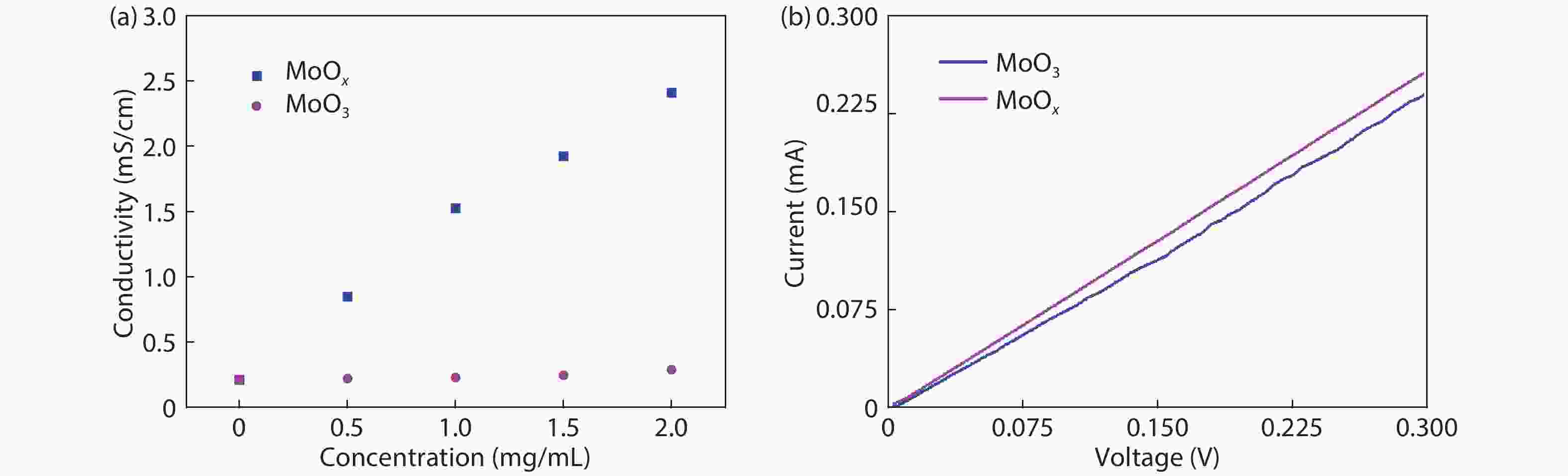
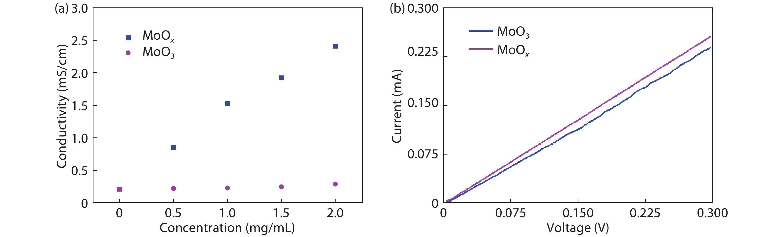
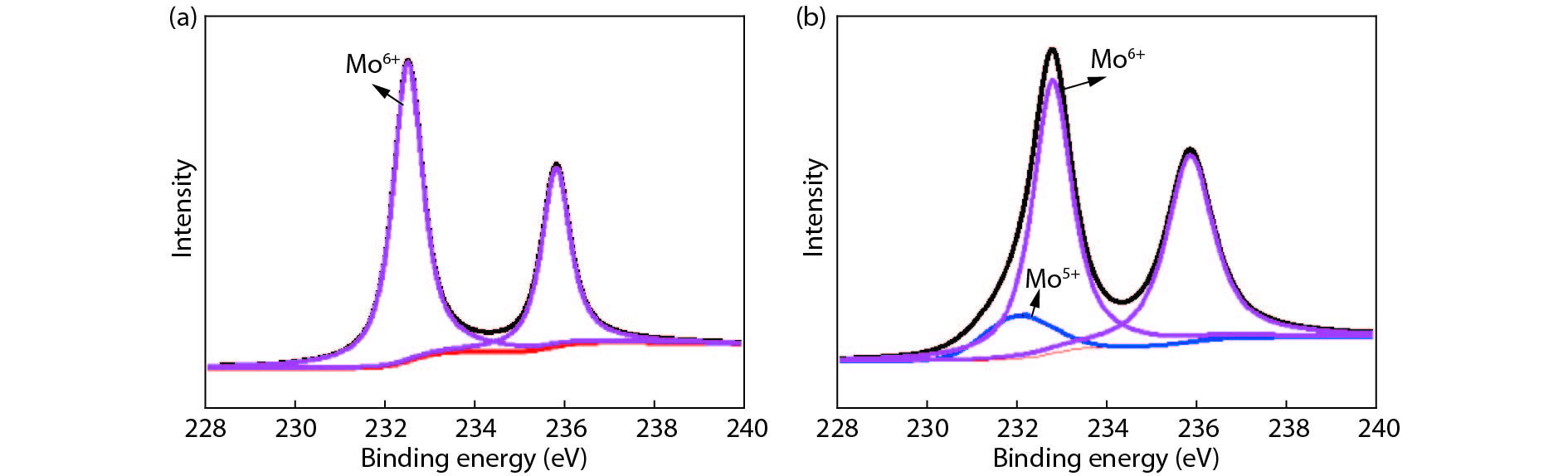
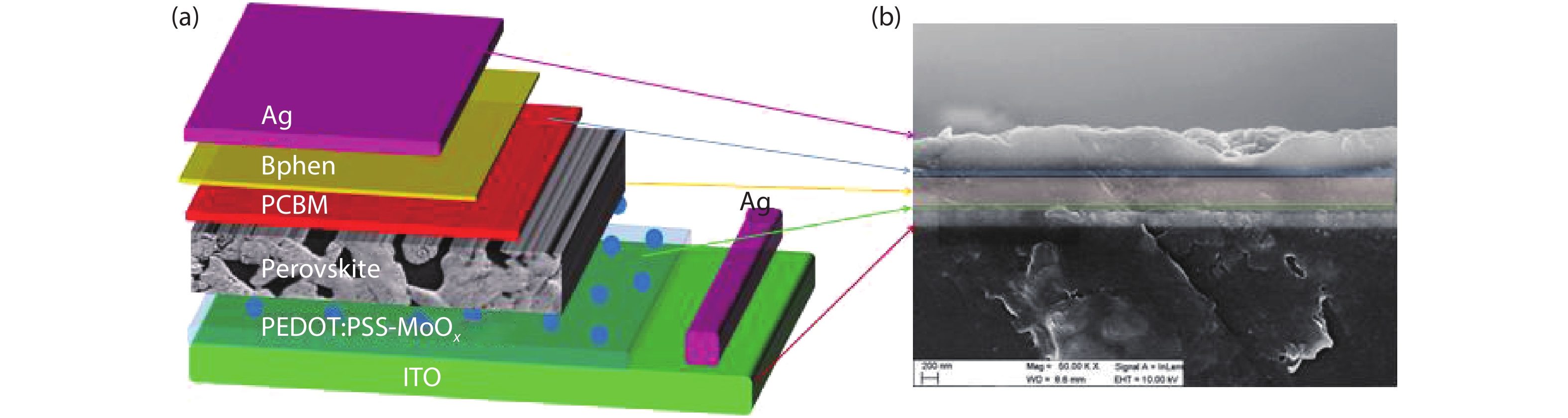
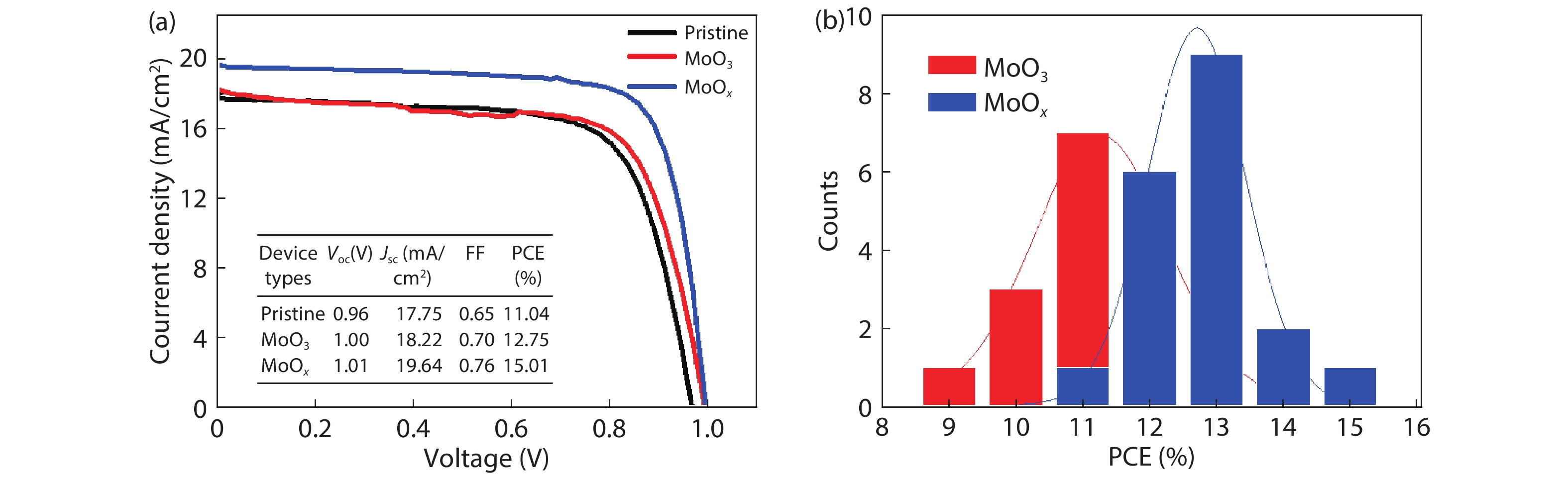
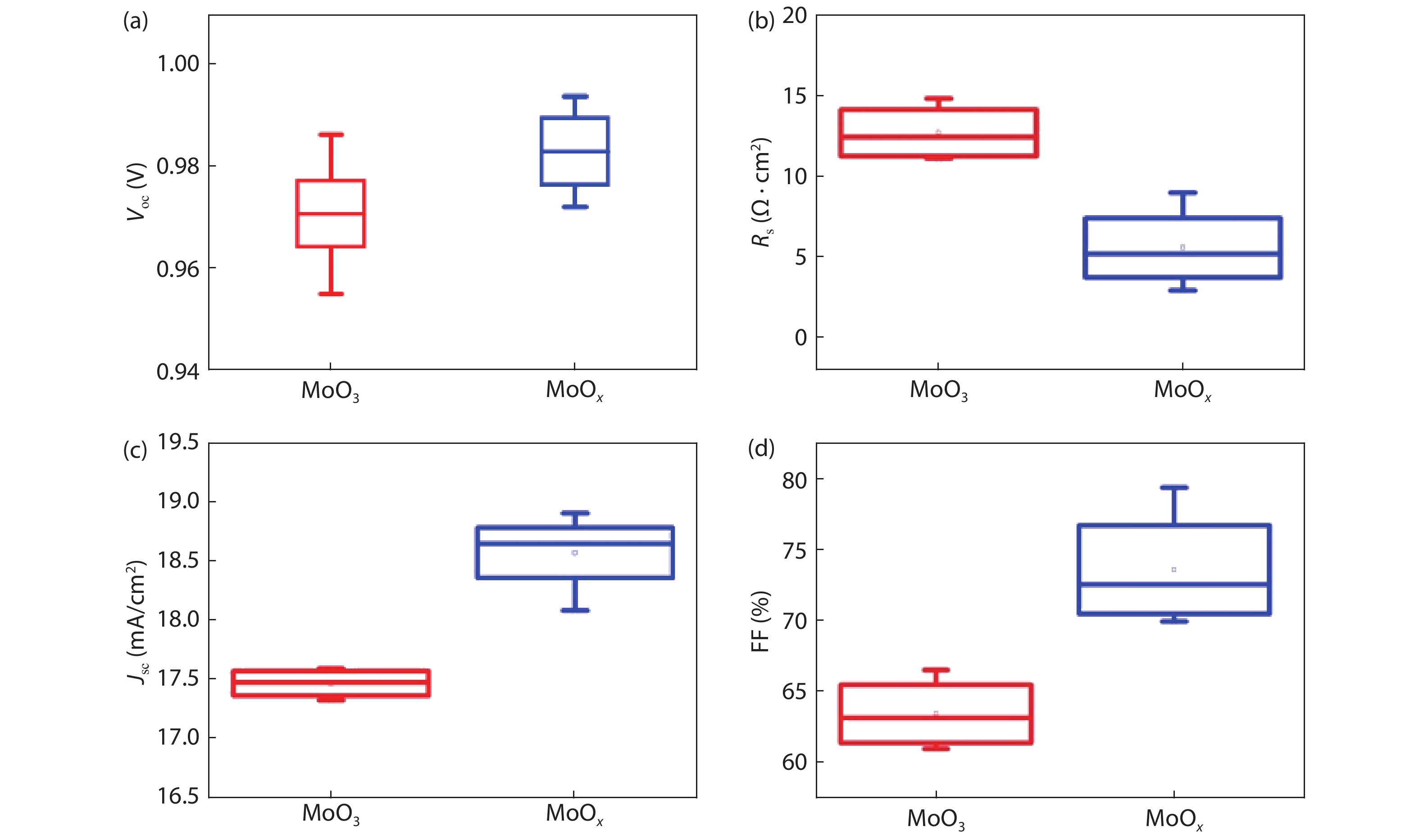
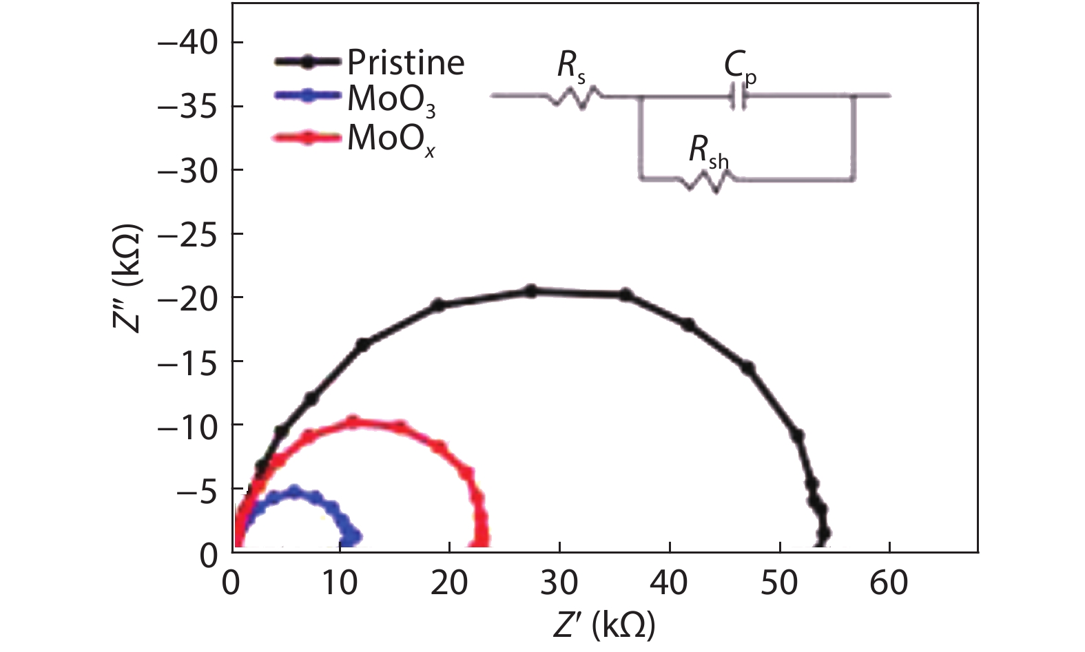
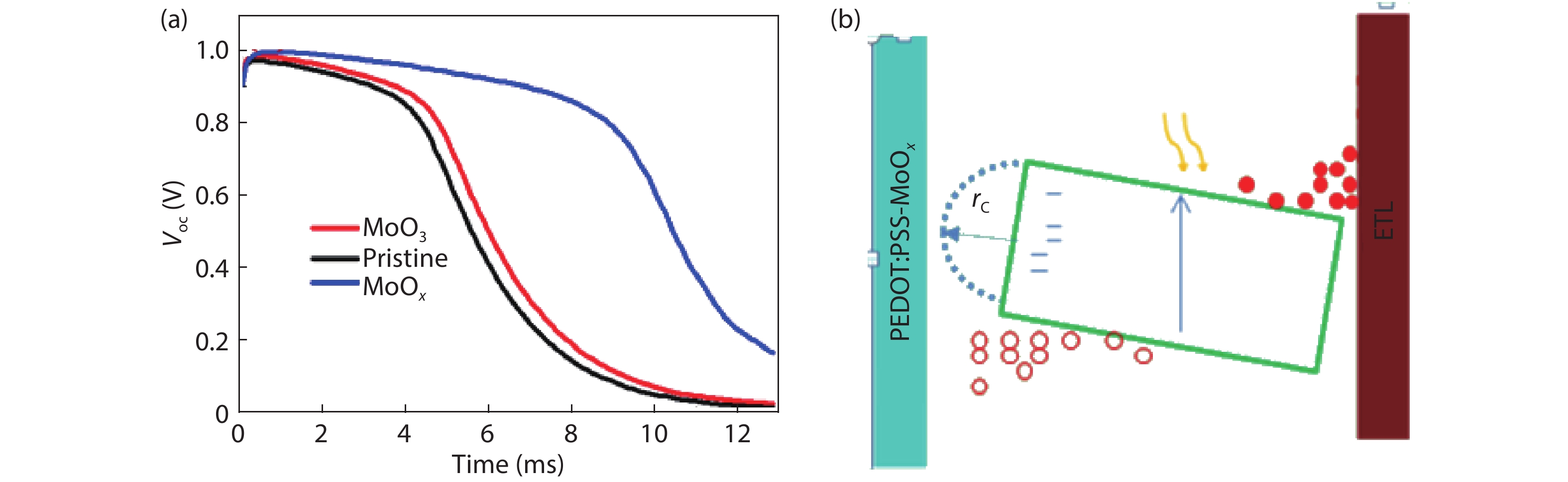
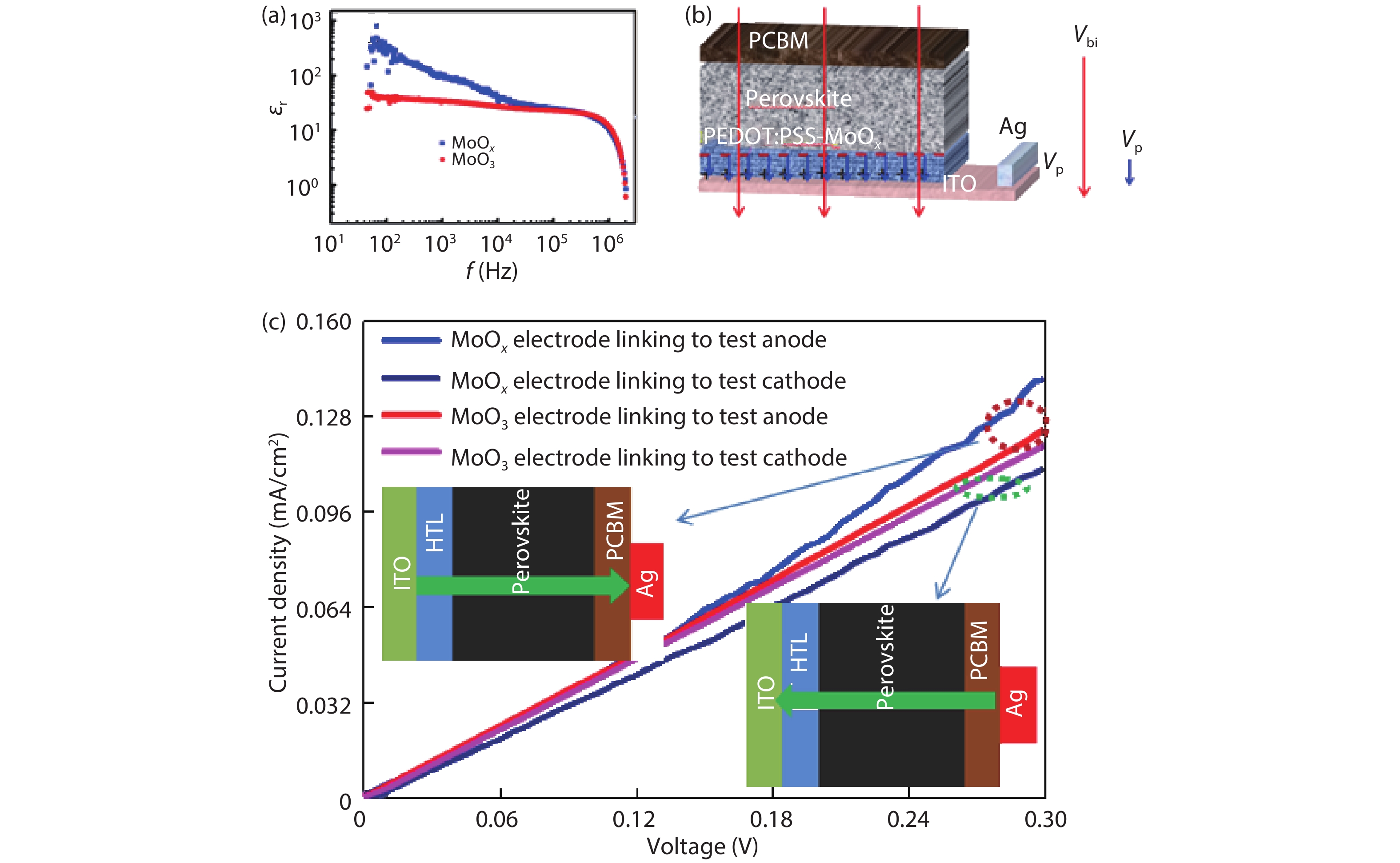
In this paper, we investigate how interface-induced polarization affects the photovoltaic performance of hybrid perovskite solar cell (PSC) devices. The polarization of the hole transport layer (HTL) is regulated through incorporating metallic-like MoOx into PEDOT:PSS. The common MoO3 doped into PEDOT:PSS is used as a reference, and the device that used PEDOT:PSS-MoOx as the HTL shows an enhanced Jsc and FF compared to the reference device. The open-circuit photovoltage decay and impedance spectroscopy measurements indicate that trap-assisted recombination is effectively suppressed at the interface between the hybrid perovskite and the PEDOT:PSS-MoOx HTL, while severe trap assisted recombination takes place at the perovskite/PEDOT:PSS and perovskite/PEDOT:PSS-MoO3 interface. We attribute these experimental findings to the fact that the incorporation of metallic-like Mo5+ into PEDOT:PSS enhances the conductivity of HTL and the interface polarization between PEDTOT:PSS layer and perovskite, which helps to induce an interface polarization electric field to facilitate separation of charges and screen the recombination between the traps and free charges.
J. Semicond.
2020, 41(5): 052204 doi: 10.1088/1674-4926/41/5/052204
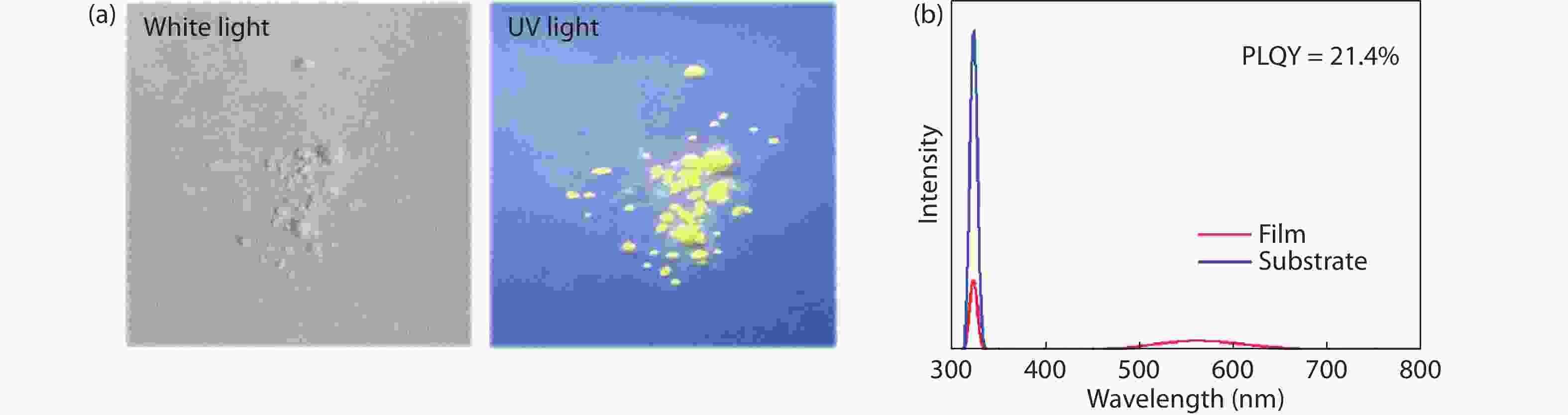
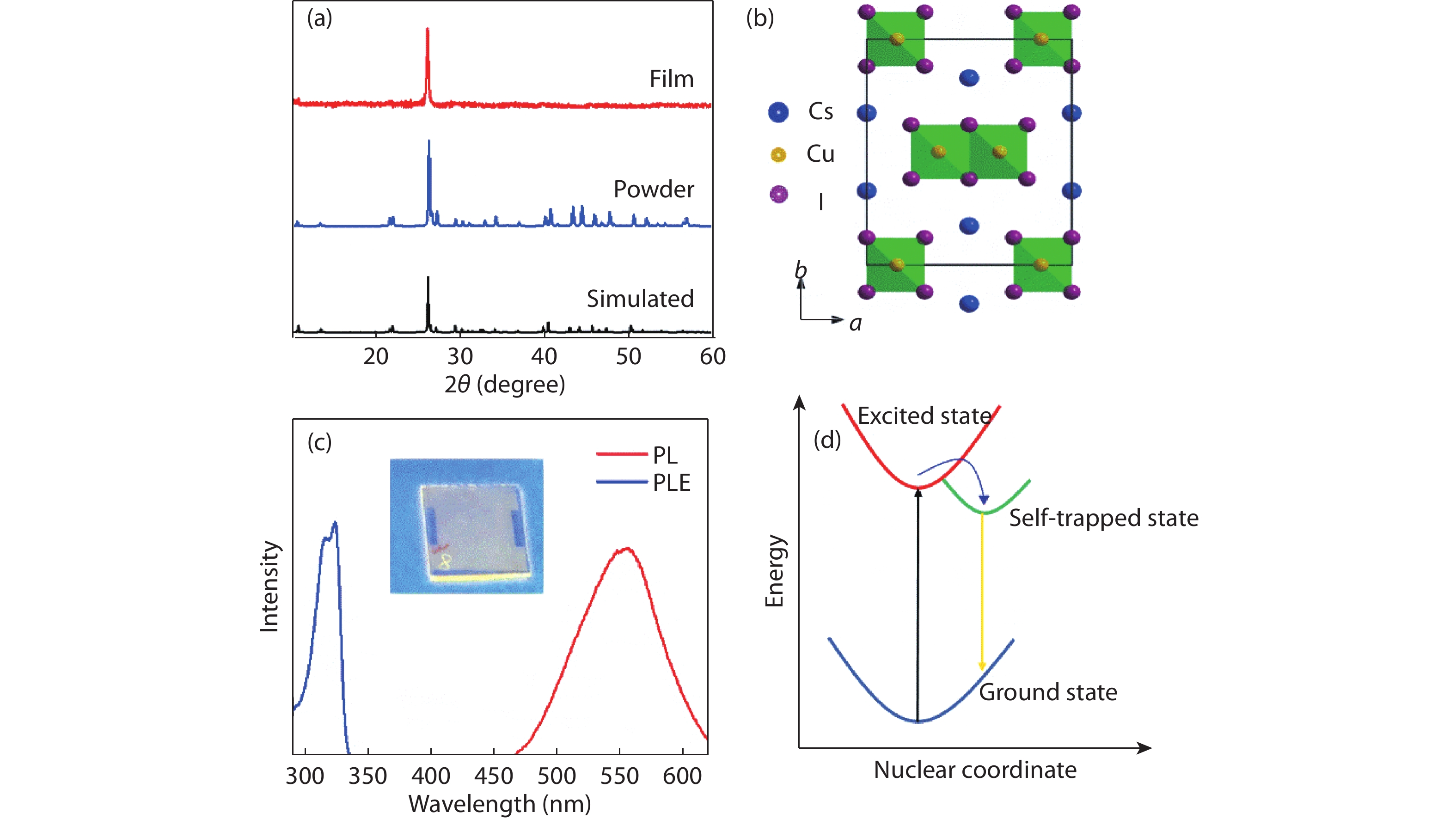
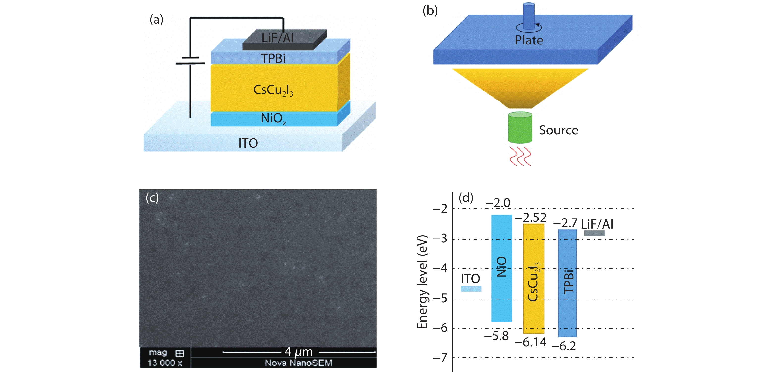
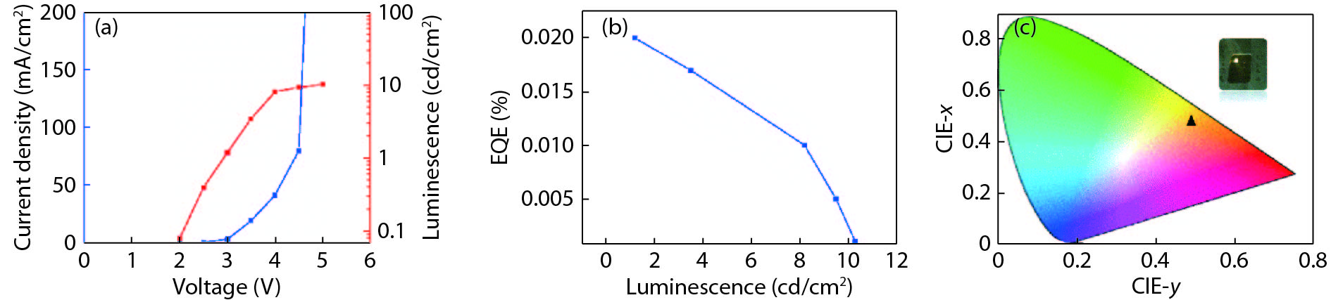
Light-emitting diodes based on lead halide perovskite have attracted great attention due to their outstanding performance. However, their application is plagued by the toxicity of Pb and the poor stability. Herein novel copper-based all inorganic perovskite CsCu2I3 with much enhanced stability has been reported with a potential photoluminescence quantum yield (PLQY) over 20% and self-trapped excitons (STE). By taking advantage of its extraordinary thermal stability, we successfully fabricate high-quality CsCu2I3 film through direct vacuum-based deposition (VBD) of CsCu2I3 powder. The resulting film shows almost the same PLQY with the synthesized powder, as well as excellent uniformity and stability. The perovskite light-emitting diodes (Pe-LED) based on the evaporated CsCu2I3 emitting layer achieve a luminescence of 10 cd/m2 and an external quantum efficiency (EQE) of 0.02%. To the best of our knowledge, this is the first CsCu2I3 Pe-LED fabricated by VBD with STE property, which offers a new avenue for lead-free Pe-LED.

J. Semicond.
2020, 41(5): 052205 doi: 10.1088/1674-4926/41/5/052205
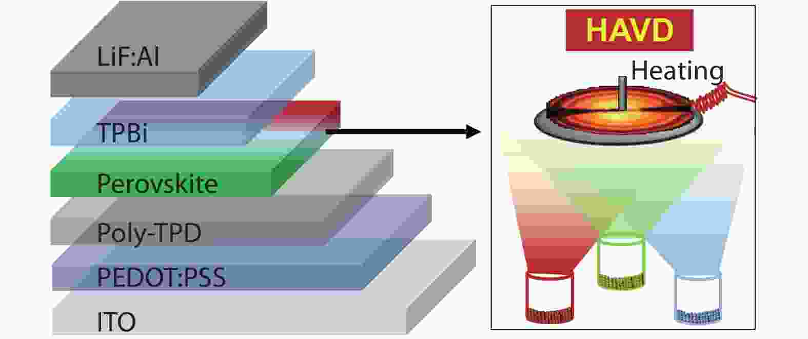
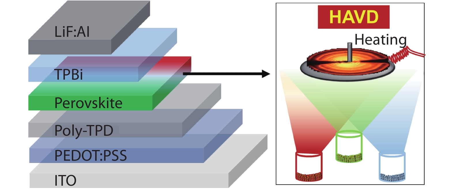
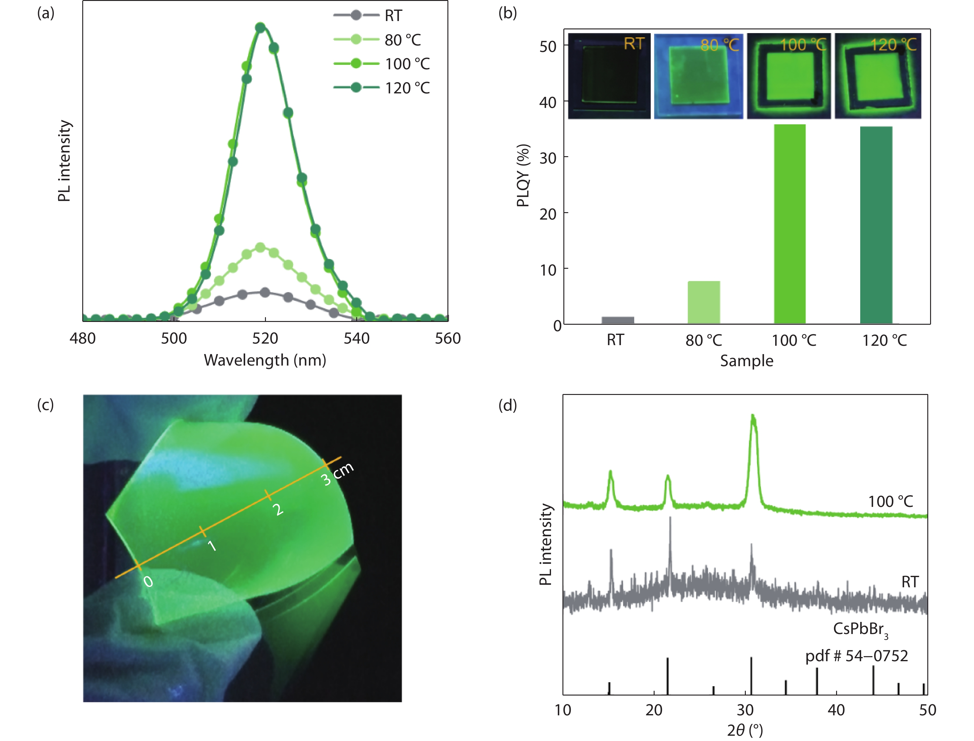
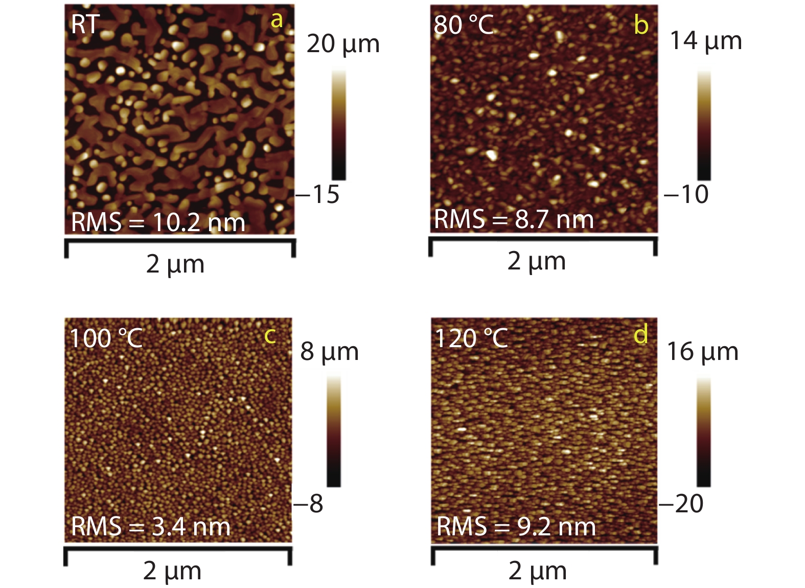
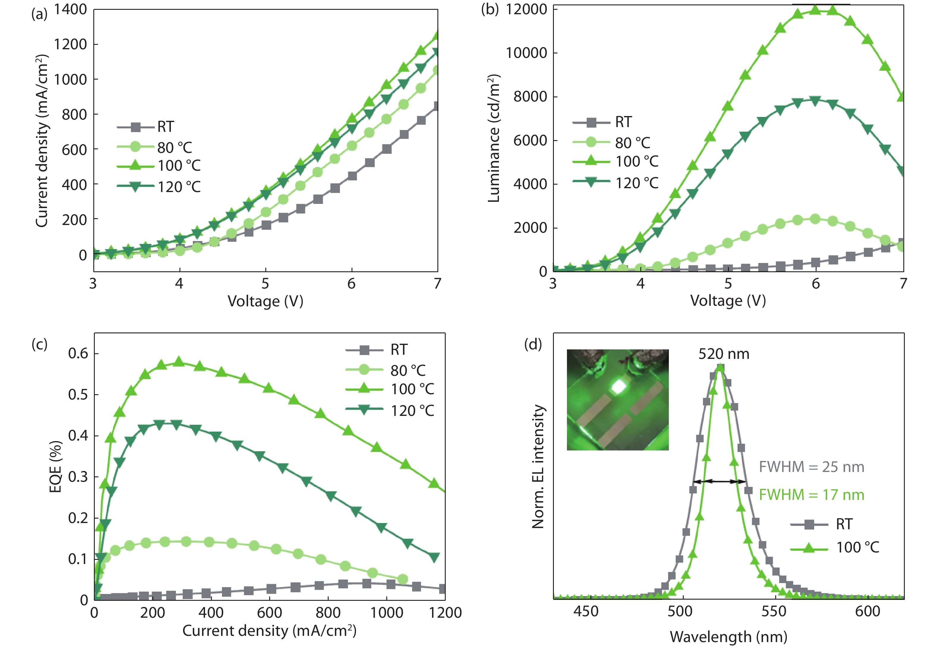
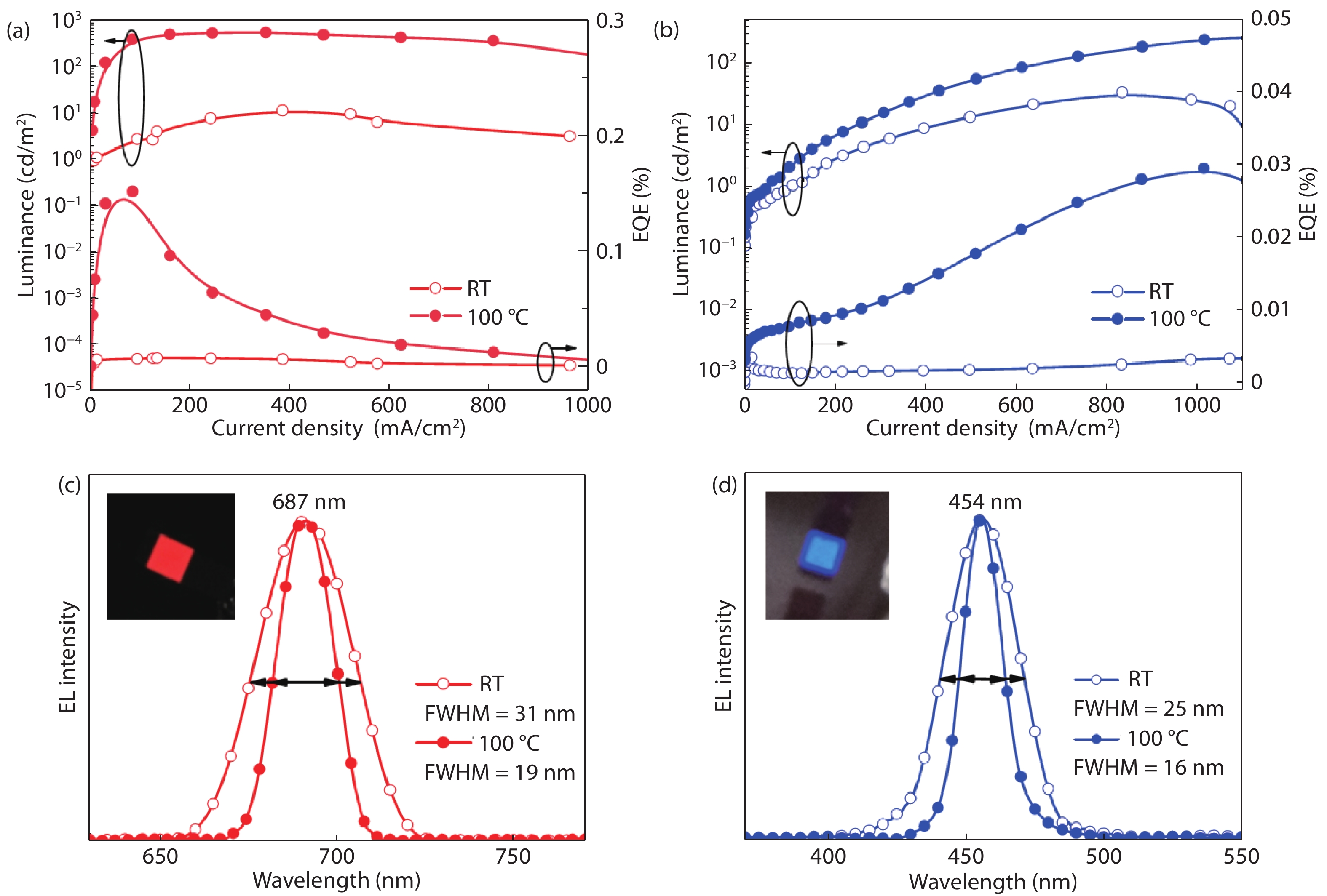
Inorganic perovskites (CsPbX3 (X = I, Br, Cl)) have broad prospection in the field of high-definition displaying due to its excellent optoelectronic characteristics. The vacuum deposition process possesses advantages and competitiveness in the industrialized production. However, the performance of light emitting diodes (LEDs) based on vacuum-deposited is incredibly low. Herein, we proposed a heating-assisted vacuum deposition (HAVD) method to construct inorganic perovskite LEDs (PeLEDs) with enhanced performance. The roughness and crystallinity of perovskite film were improved by regulating the heating treatment of substrates. And the perovskite film exhibited largely rise in luminescence, with decreasing defect density. Consequently, with the optimized temperature, the green PeLEDs exhibited 100-fold improvement of external quantum efficiency (EQE) with the luminance of up to 11 941 cd/m2, and the full width at half-maximum (FWHM) of the electroluminescence (EL) spectra was decreased from 25 to 17 nm. At the same time, the red and blue PeLEDs also exhibited obvious enhancement in EQE and luminance by HAVD method, and both the FWHM of EL spectra dropped below 20 nm, exhibiting excellent high color purity. HAVD strategy has a huge potential to be a new commonly used method for low-cost fabrication of displays and lighting.

J. Semicond.
2020, 41(5): 052206 doi: 10.1088/1674-4926/41/5/052206
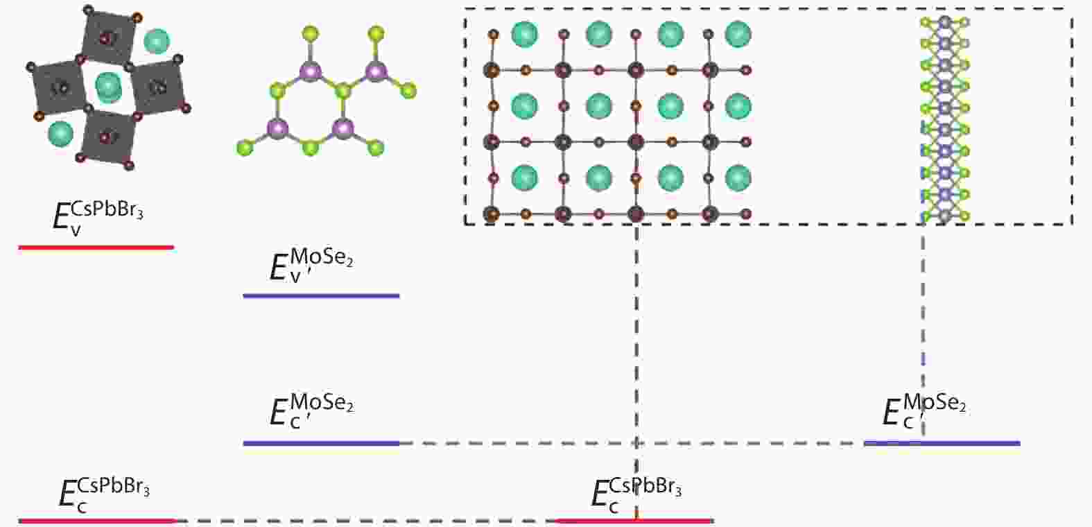
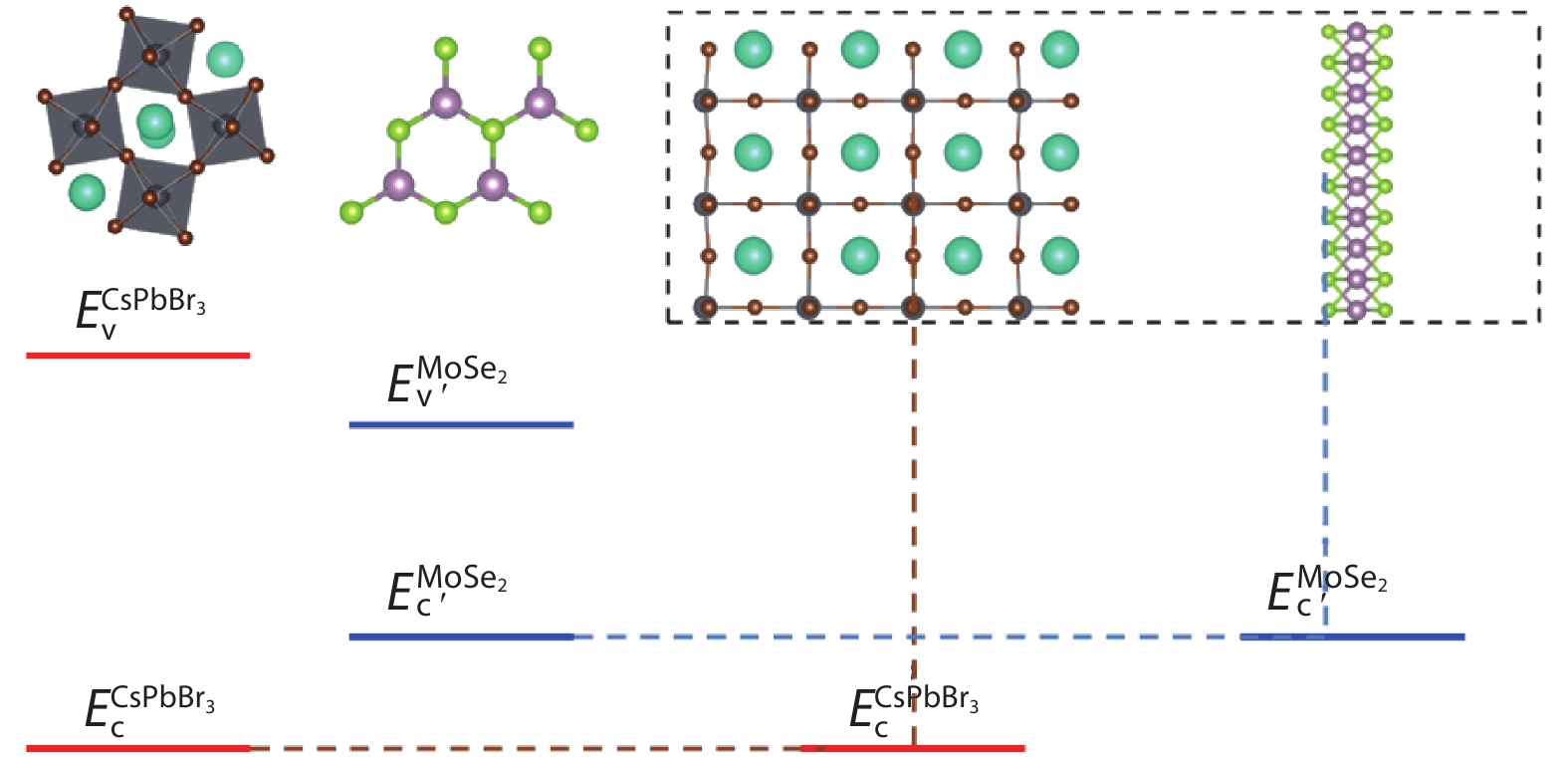
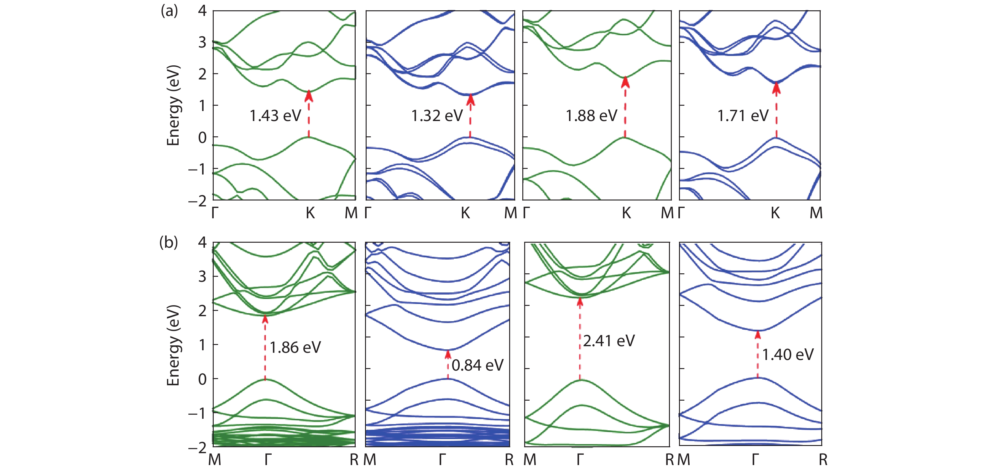
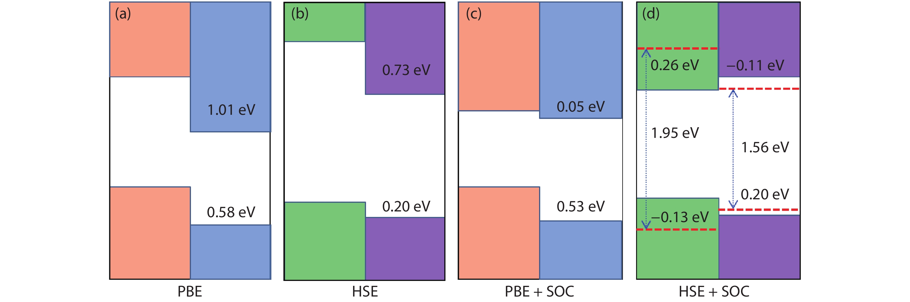
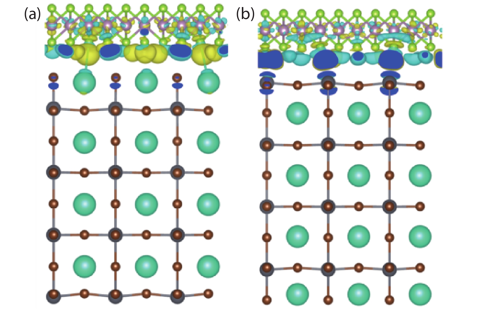
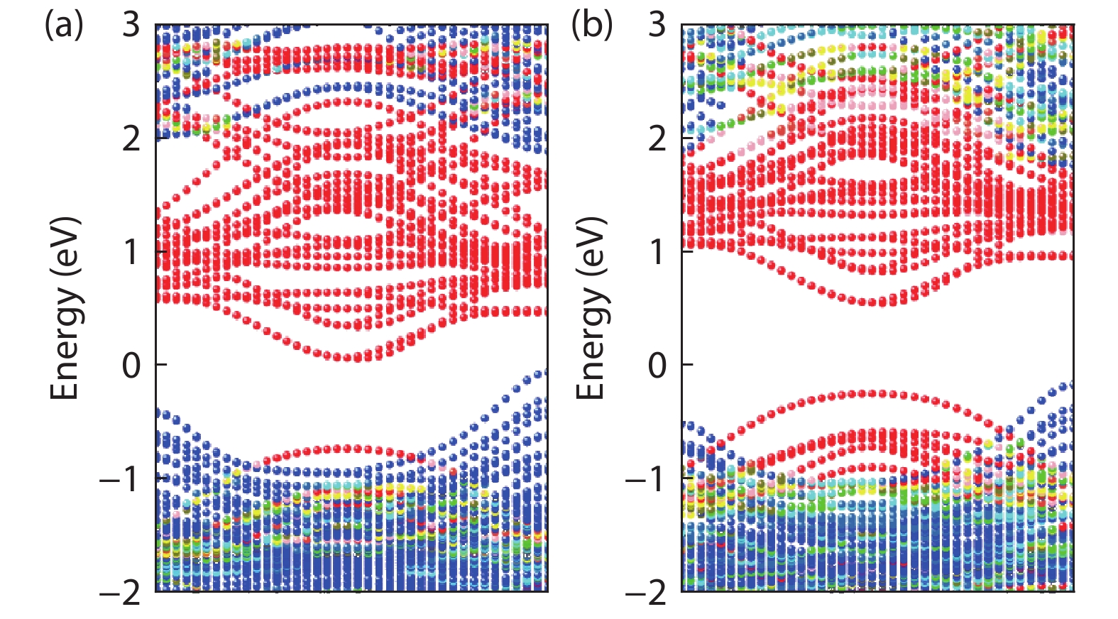
The distinguished electronic and optical properties of lead halide perovskites (LHPs) make them good candidates for active layer in optoelectronic devices. Integrating LHPs and two-dimensional (2D) transition metal dichalcogenides (TMDs) provides opportunities for achieving increased performance in heterostructured LHPs/TMDs based optoelectronic devices. The electronic structures of LHPs/TMDs heterostructures, such as the band offsets and interfacial interaction, are of fundamental and technological interest. Here CsPbBr3 and MoSe2 are taken as prototypes of LHPs and 2D TMDs to investigate the band alignment and interfacial coupling between them. Our GGA-PBE and HSE06 calculations reveal an intrinsic type-II band alignment between CsPbBr3 and MoSe2. This type-II band alignment suggests that the performance of CsPbBr3-based photodetectors can be improved by incorporating MoSe2 monolayer. Furthermore, the absence of deep defect states at CsPbBr3/MoSe2 interfaces is also beneficial to the better performance of photodetectors based on CsPbBr3/MoSe2 heterostructure. This work not only offers insights into the improved performance of photodetectors based on LHPs/TMDs heterostructures but it also provides guidelines for designing high-efficiency optoelectronic devices based on LHPs/TMDs heterostructures.