Issue Browser
Volume 41, Issue 4,
Apr 2020
Column

J. Semicond.
2020, 41(4): 041601 doi: 10.1088/1674-4926/41/4/041601

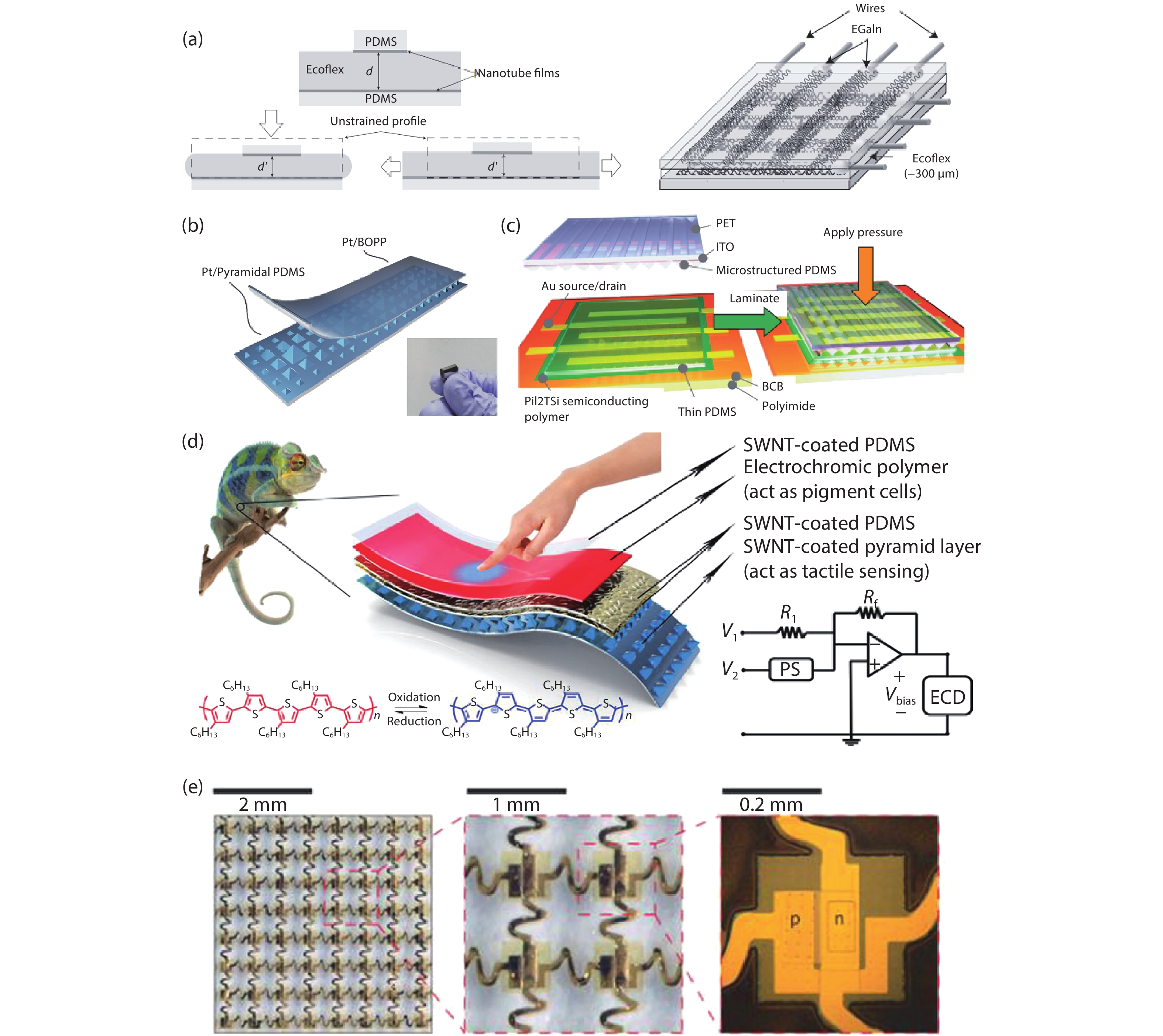
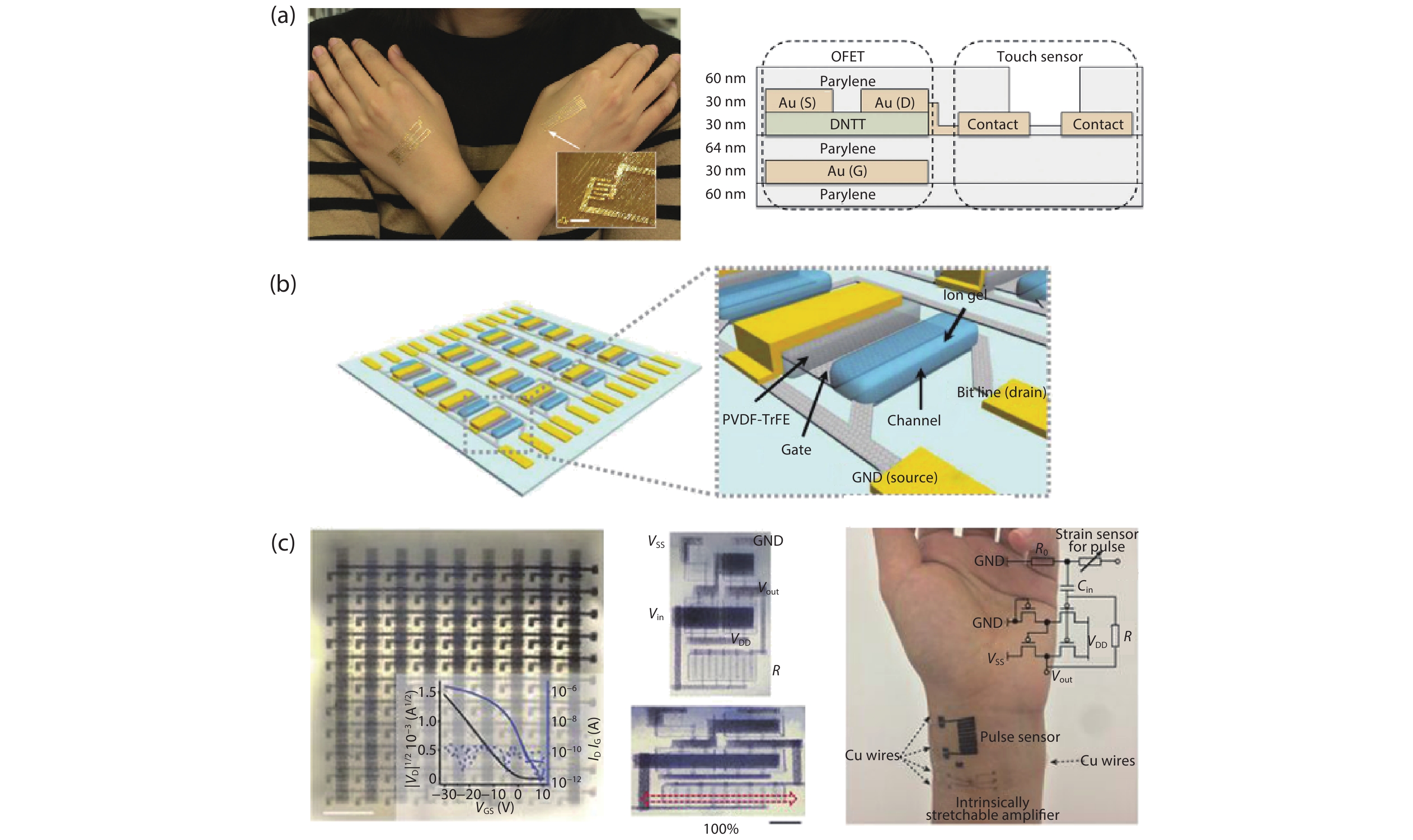
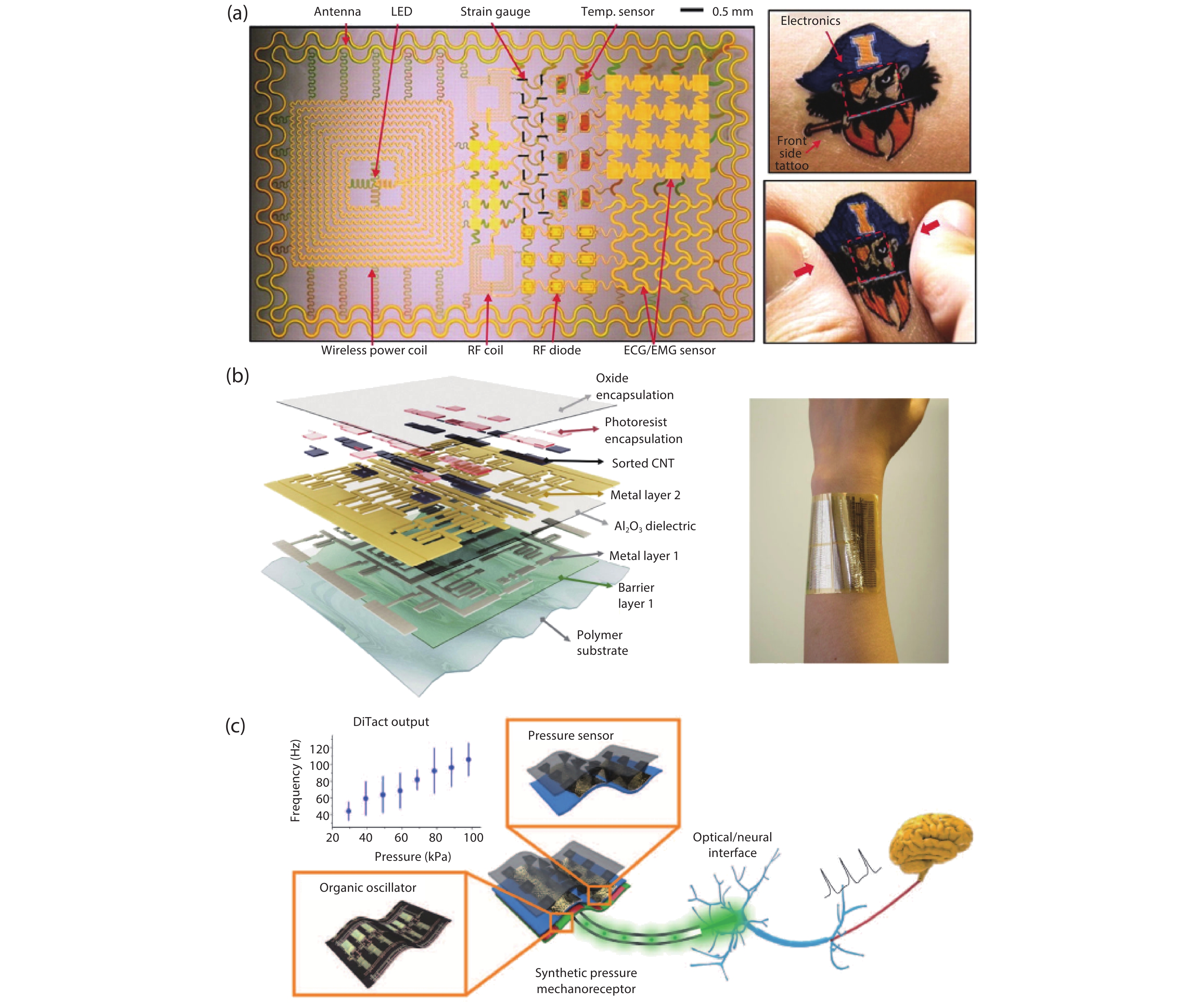
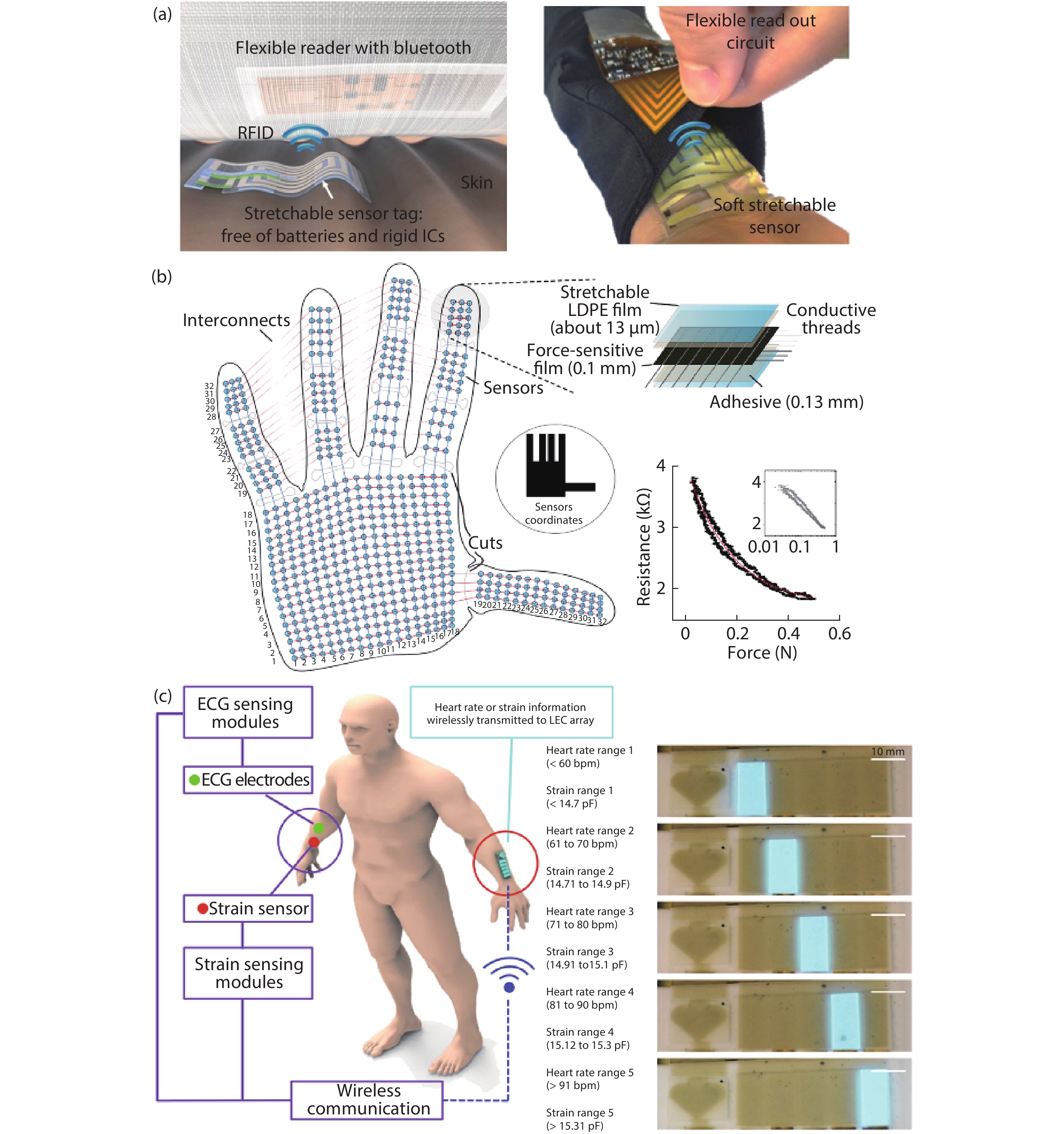
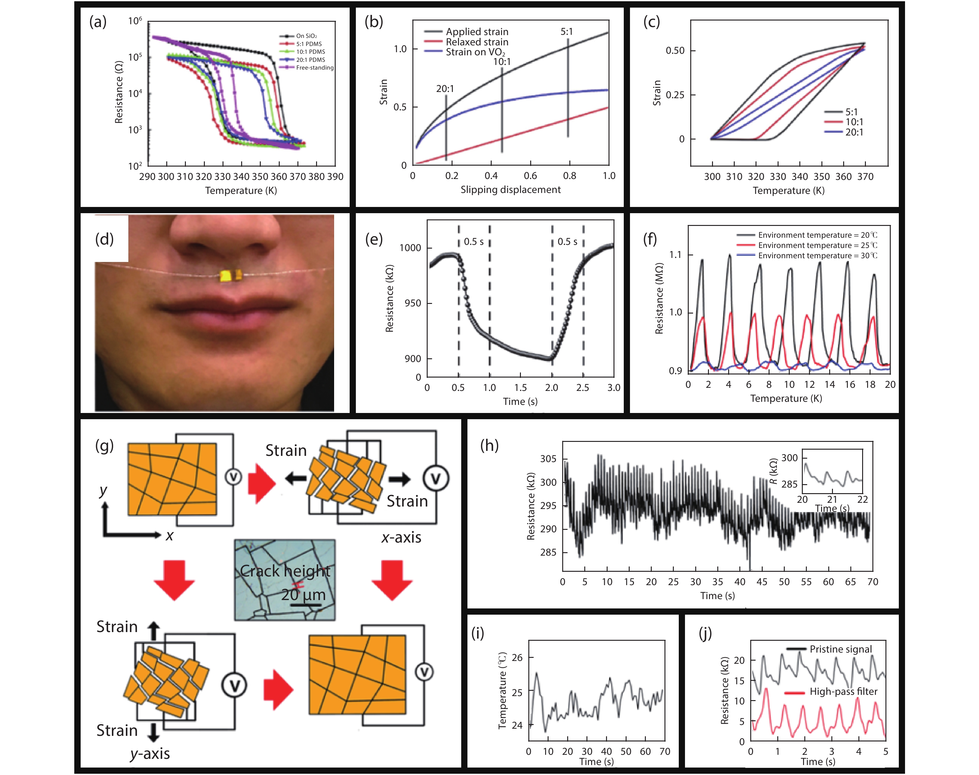
Current electronics are driven by advanced microfabrication for fast and efficient information processing. In spite of high performance, these wafer-based devices are rigid, non-degradable, and unable to autonomous repair. Skin-inspired electronics have emerged as a new class of devices and systems for next-generation flexible and wearable electronics. The technology gains inspiration from the structures, properties, and sensing mechanisms of the skin, which may find a broad range of applications in cutting-edge fields such as healthcare monitoring, human-machine interface, and soft robotics/prostheses. Practical demands have fueled the development of electronic materials with skin-like properties in terms of stretchability, self-healing capability, and biodegradability. These materials provide the basis for functional sensors with innovative and biomimetic designs. Further system-level integrations and optimizations enable new forms of electronics for real-world applications. This review summarizes recent advancements in this active area and speculates on future directions.
J. Semicond.
2020, 41(4): 041602 doi: 10.1088/1674-4926/41/4/041602
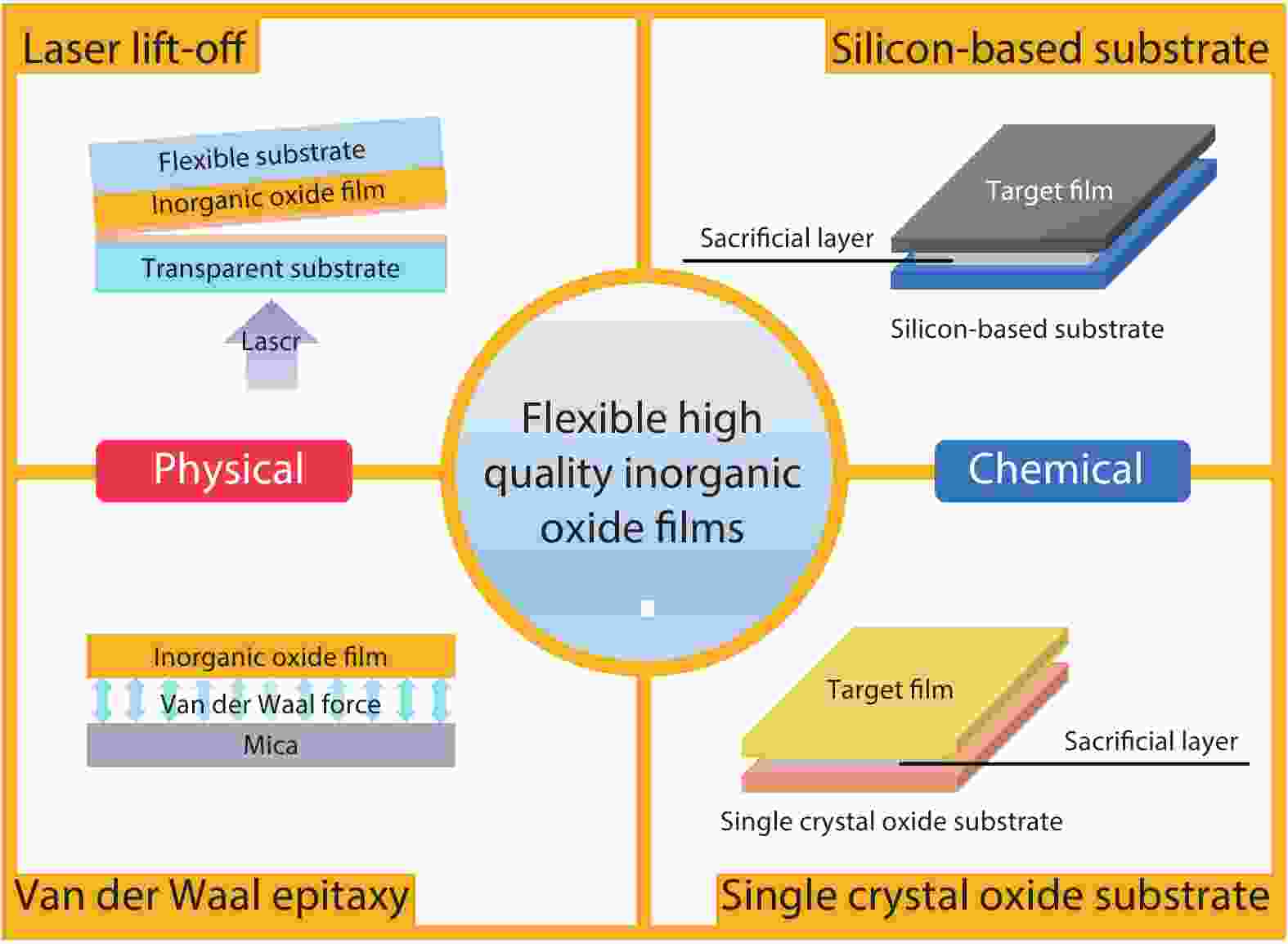
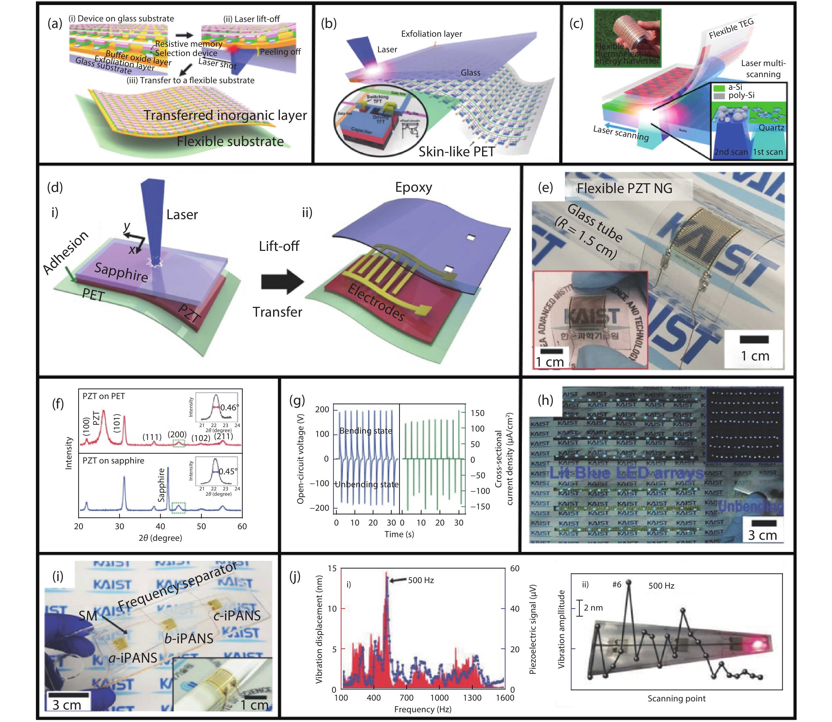
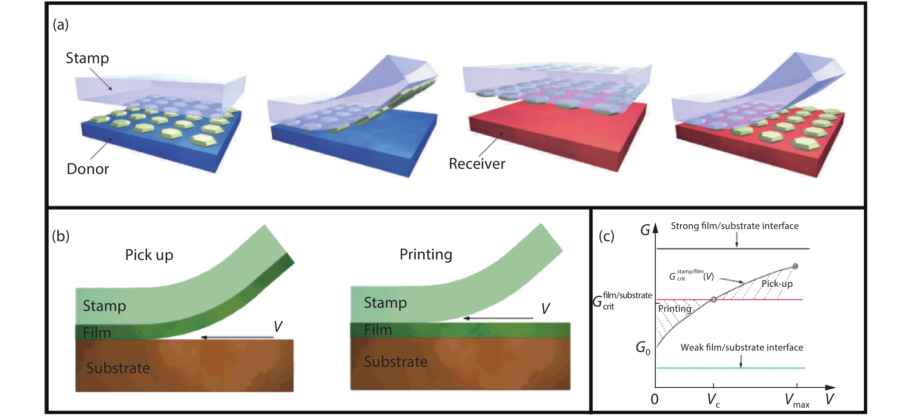
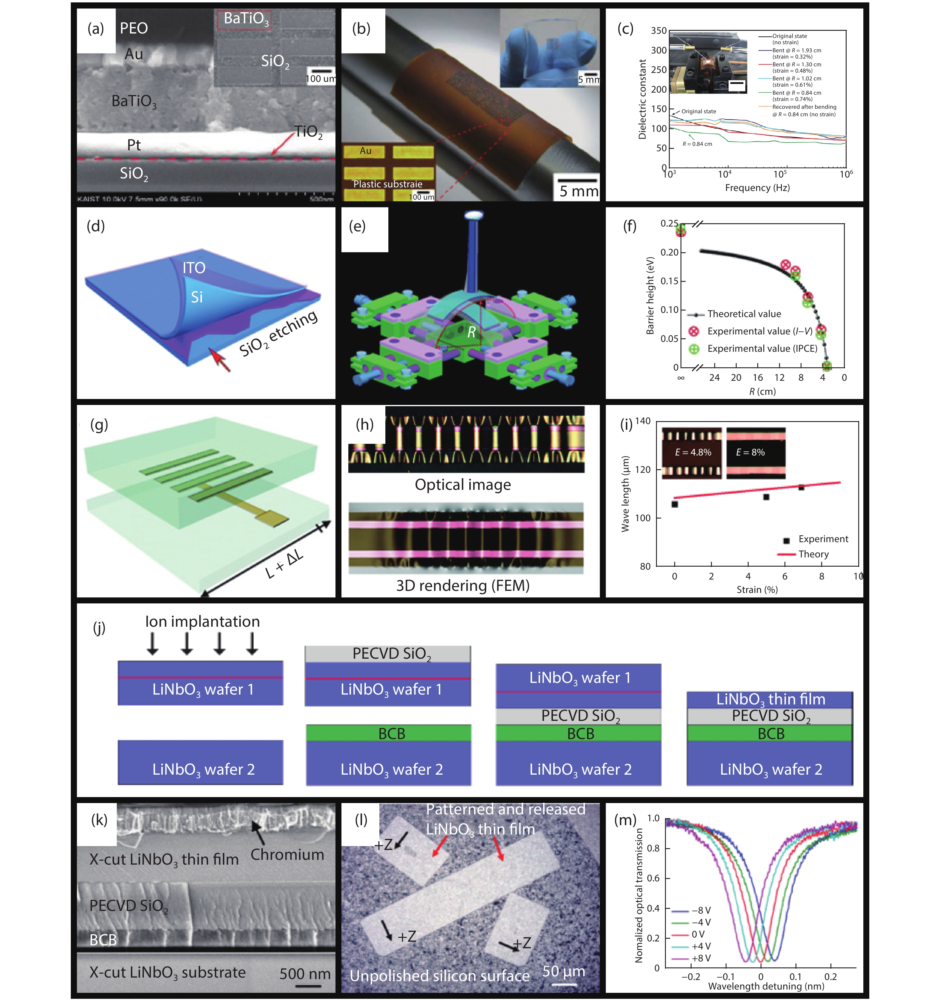
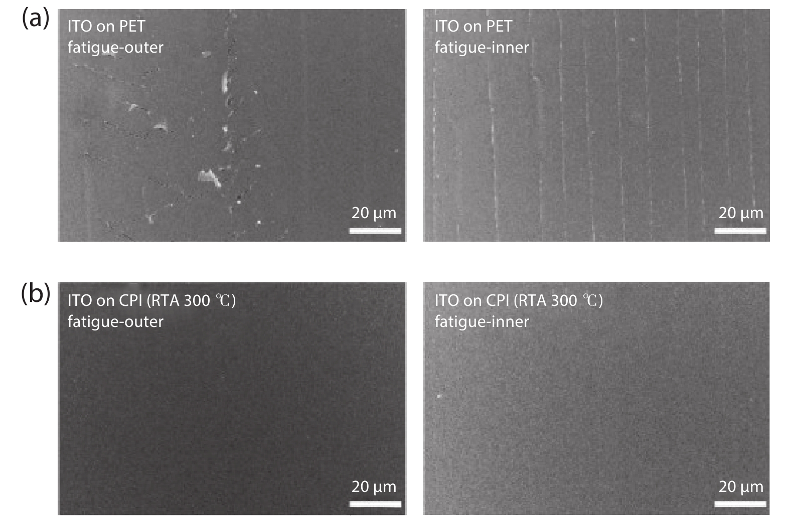
With the advent of human-friendly intelligent life, as well as increasing demands for natural and seamless human-machine interactions, flexibility and wearability are among the inevitable development trends for electronic devices in the future. Due to the advantages of rich physicochemical properties, flexible and stretchable inorganic oxide thin-film electronics play an increasingly important role in the emerging and exciting flexible electronic field, and they will act as a critical player in next-generation electronics. However, a stable strategy to render flexibility while maintaining excellent performance of oxide thin films is the most demanding and challenging problem, both for academic and industrial communities. Thus, this review focuses on the latest advanced strategies to achieve flexible inorganic oxide thin-film electronics. This review emphasizes the physical transferring strategies that are based on mechanical peeling and the chemical transferring strategies that are based on sacrificial layer etching. Finally, this review evaluates and summarizes the merits and demerits of these strategies toward actual applications, concluding with a future perspective into the challenges and opportunities for the next-generation of flexible inorganic oxide thin-film electronics.


J. Semicond.
2020, 41(4): 041603 doi: 10.1088/1674-4926/41/4/041603
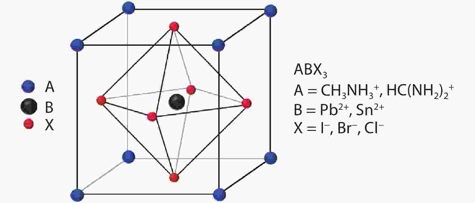
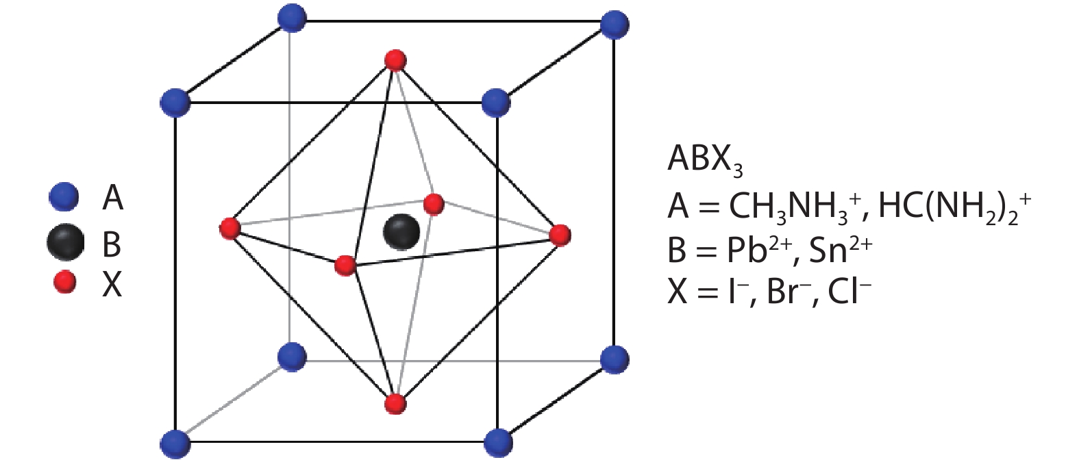
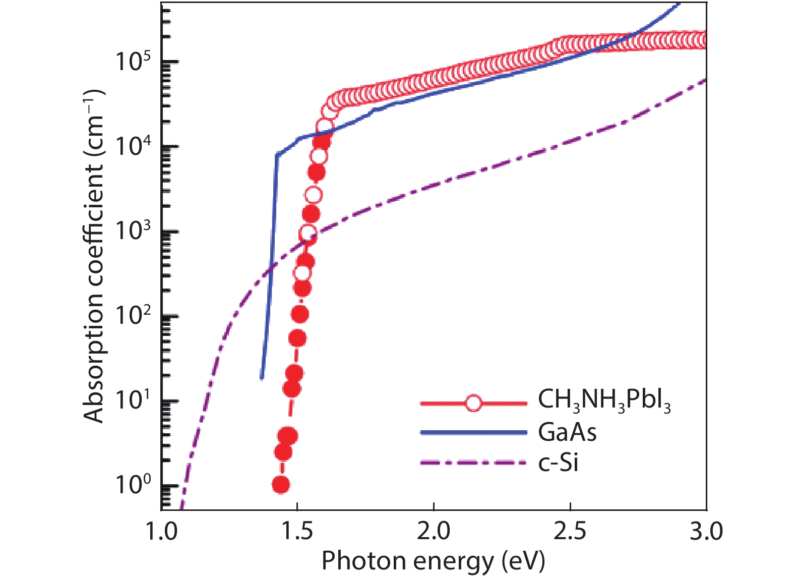
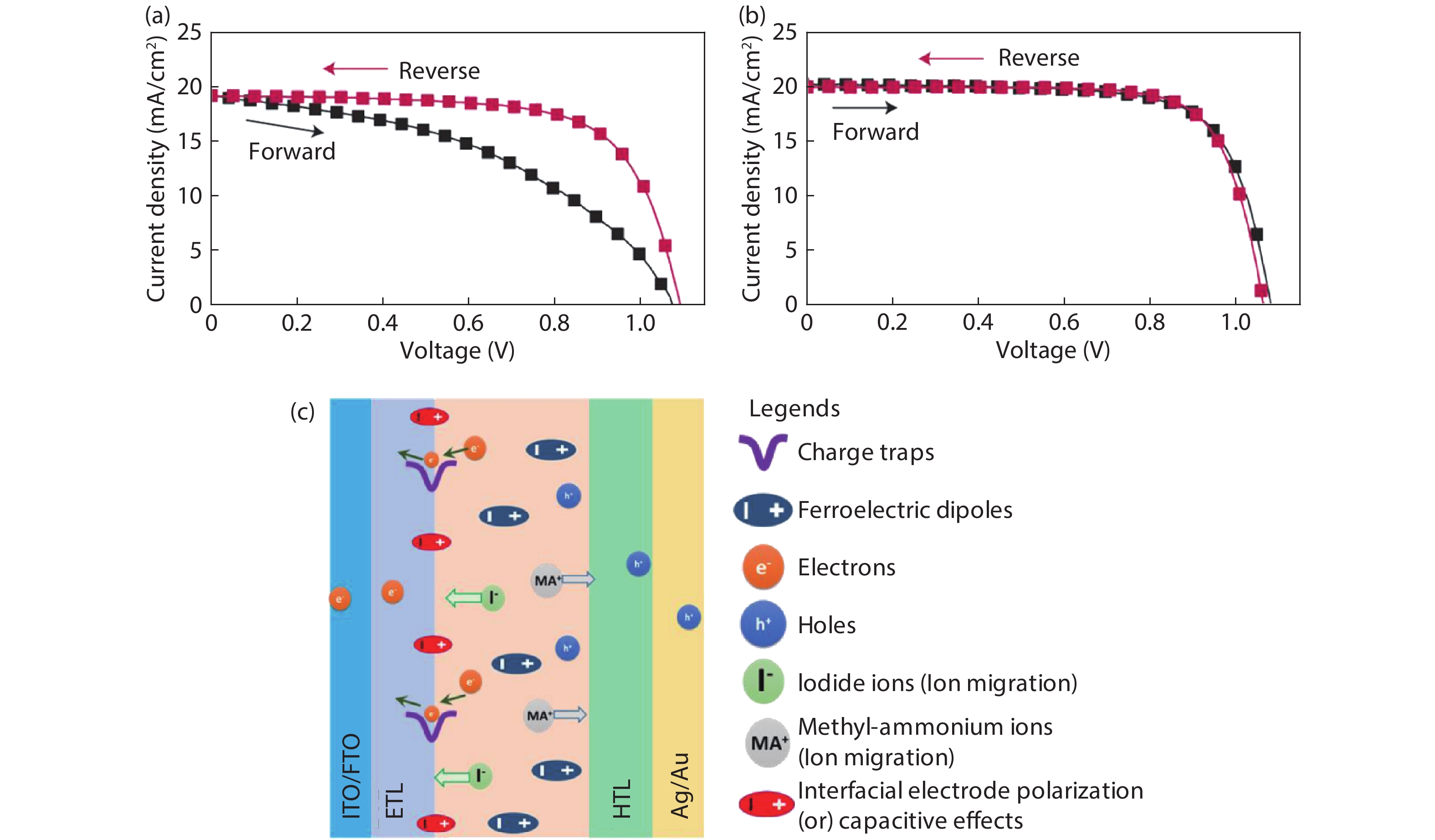
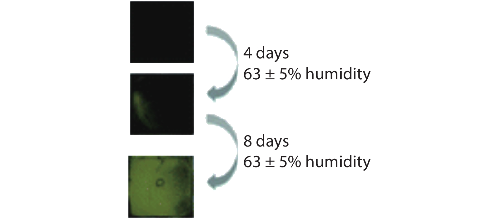
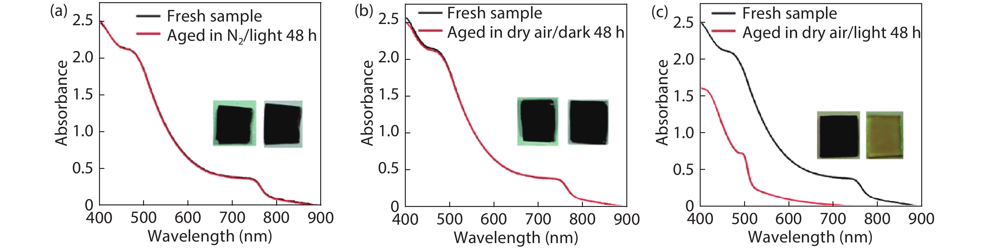
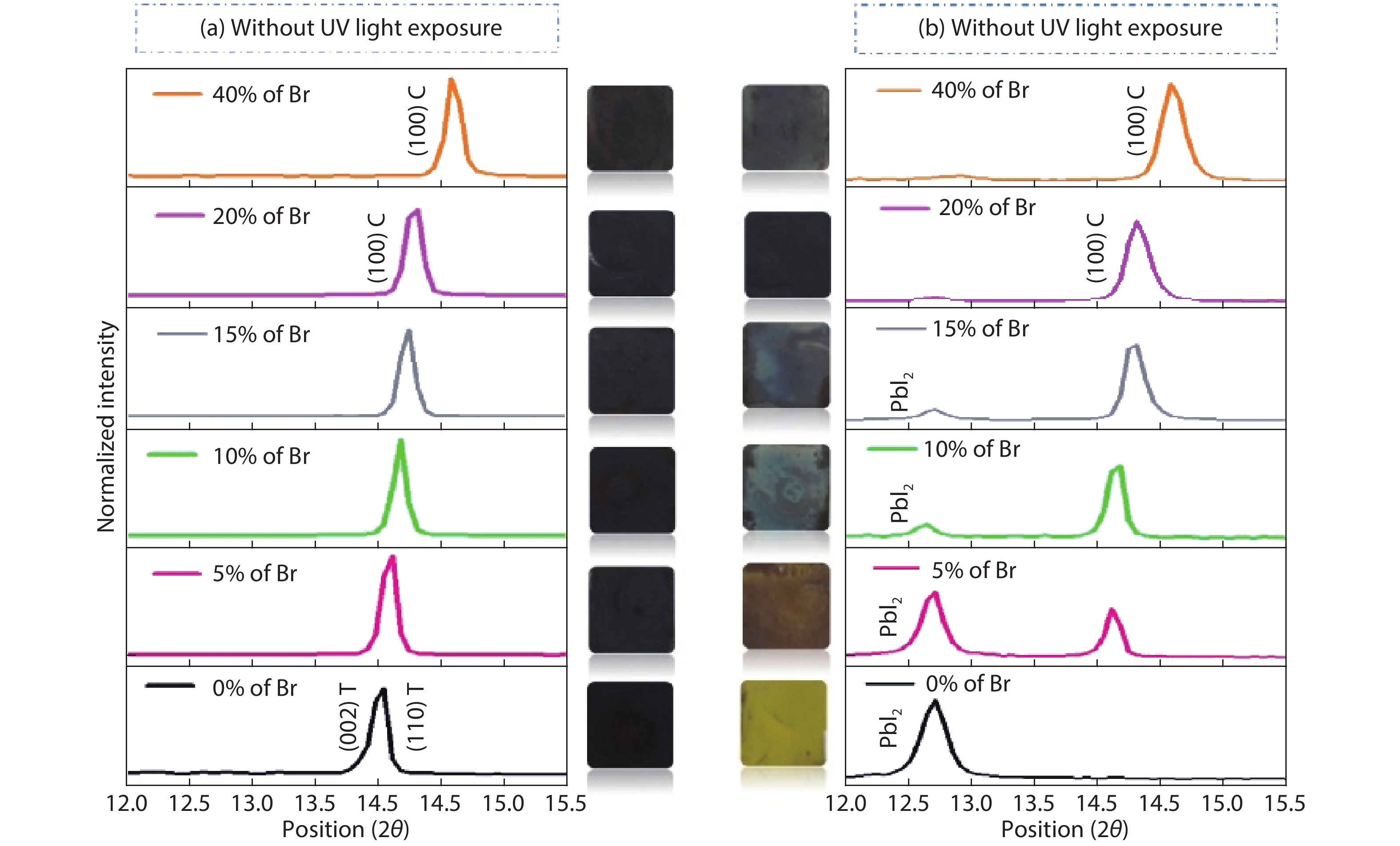
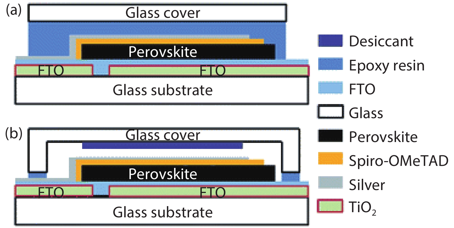
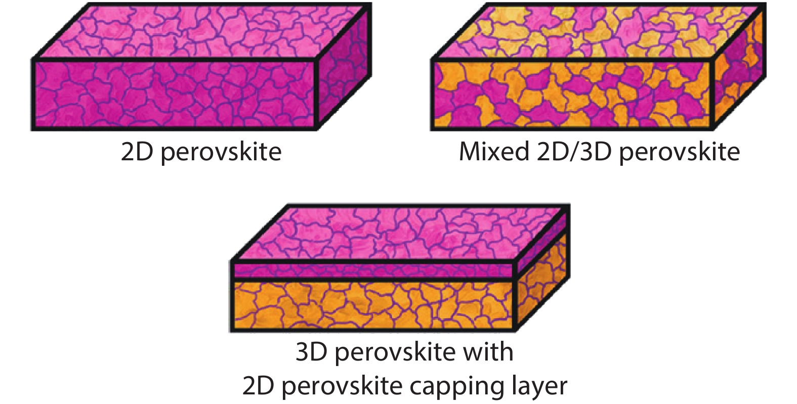
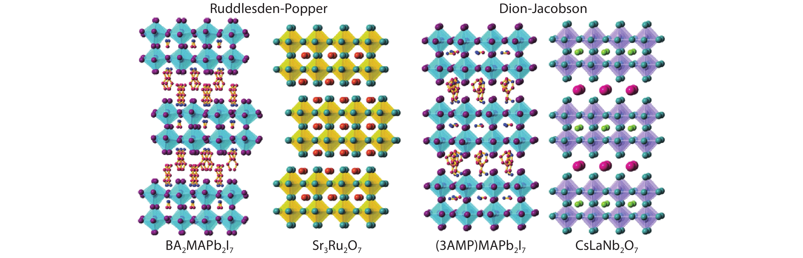
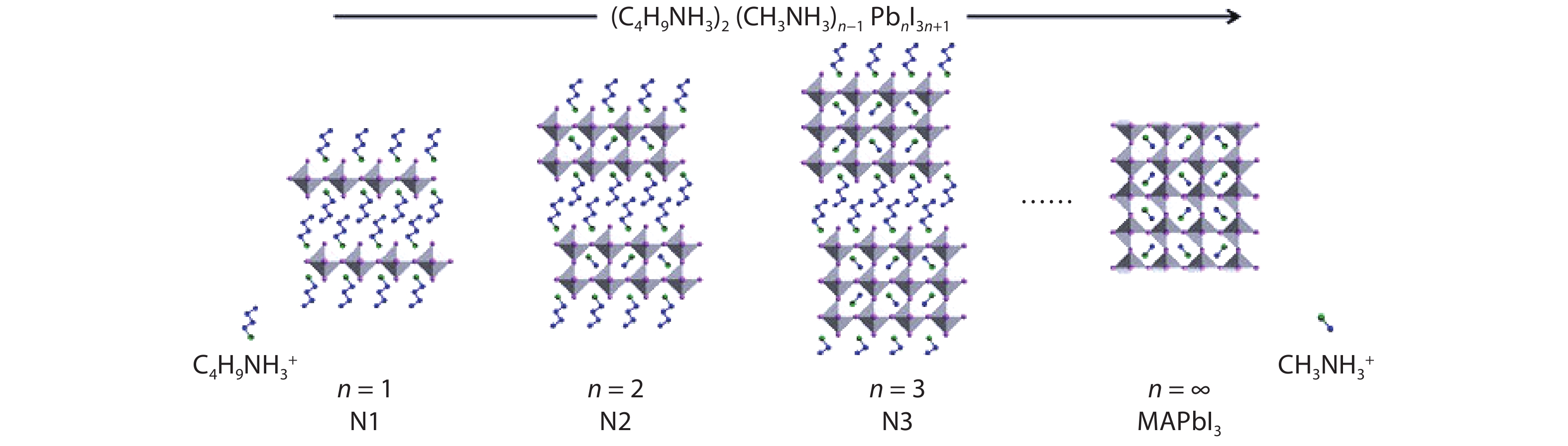
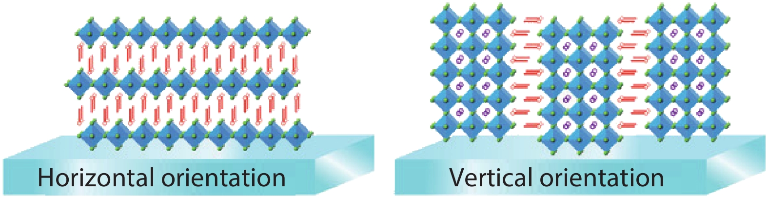
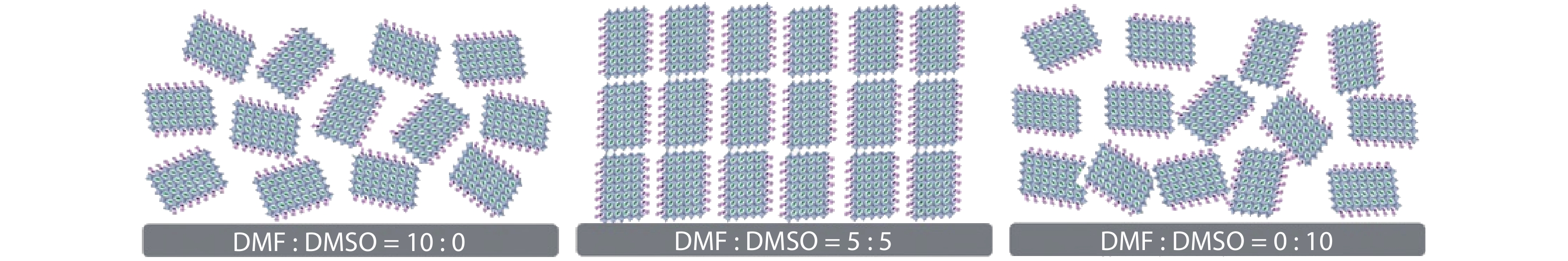
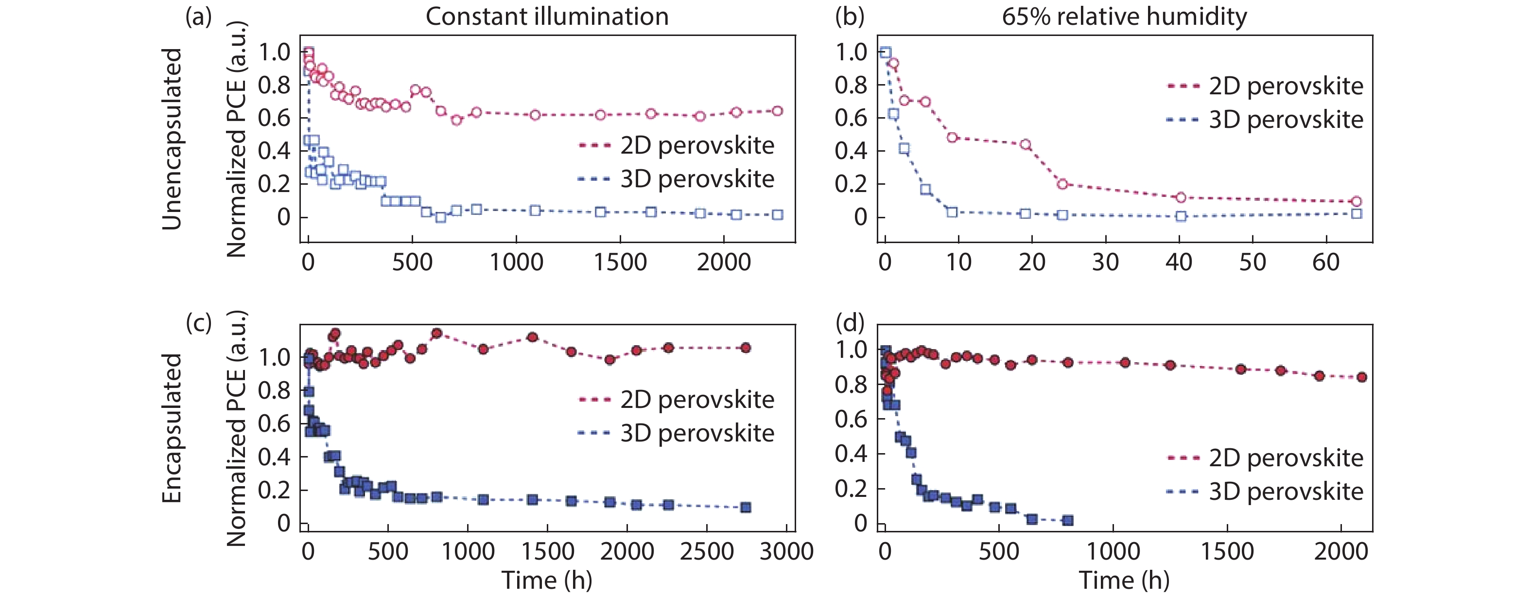
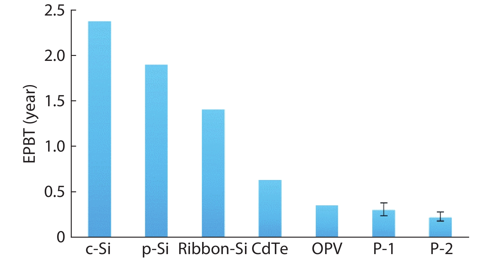
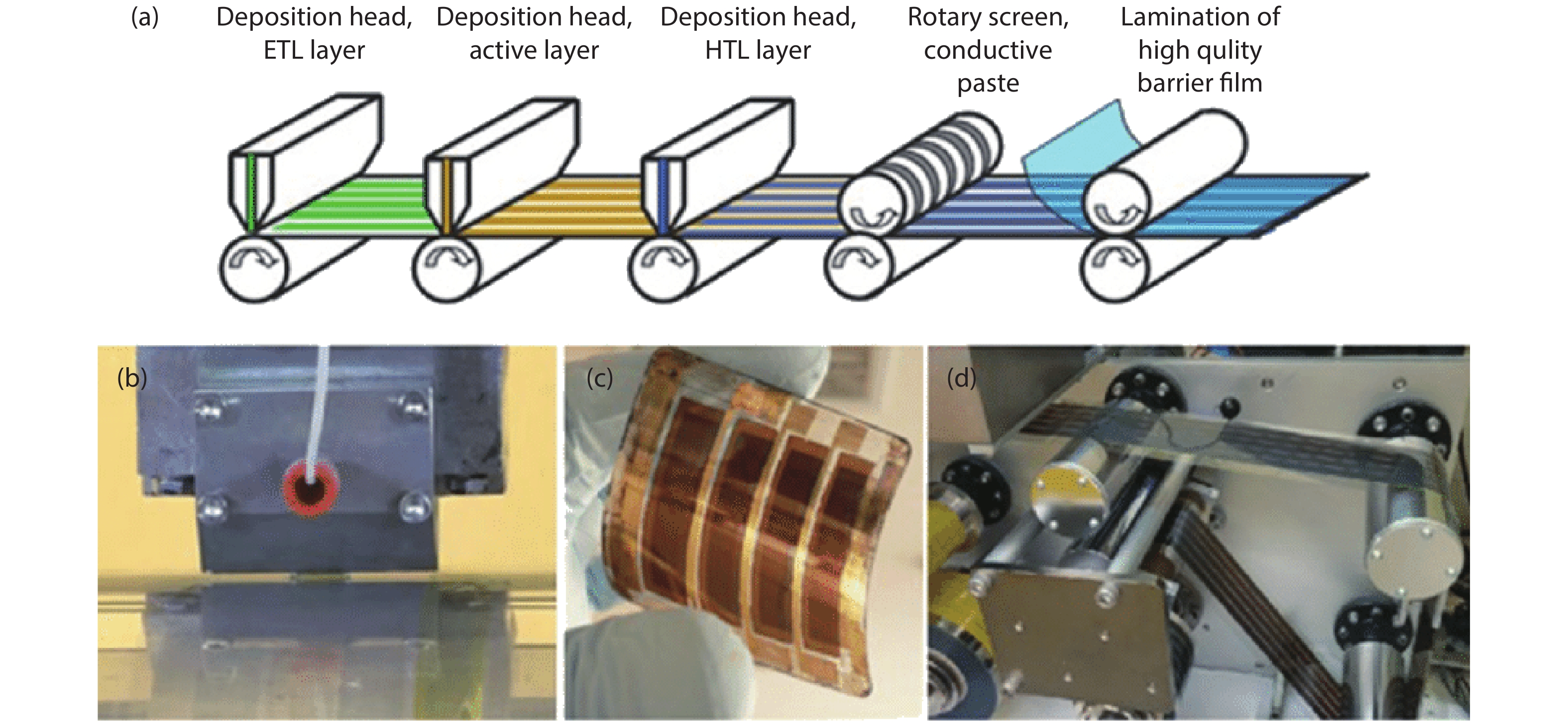
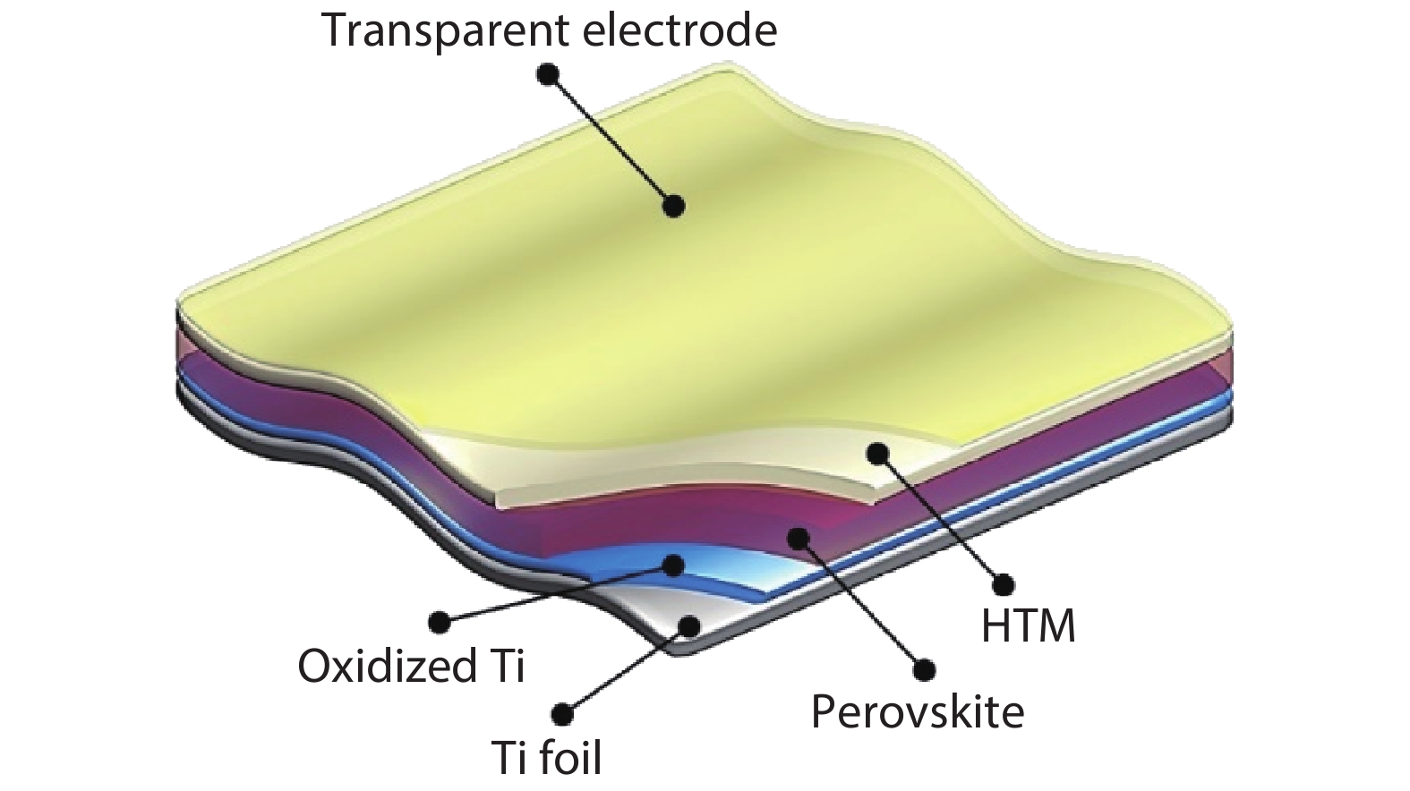
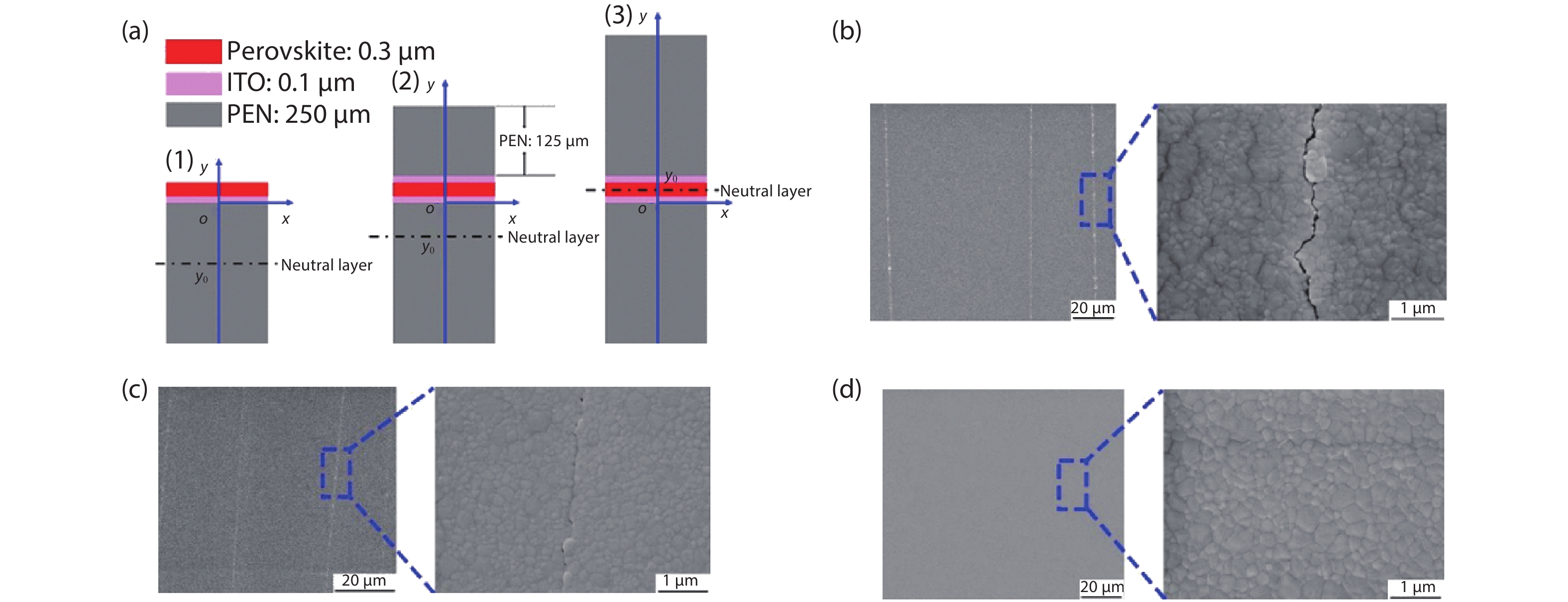
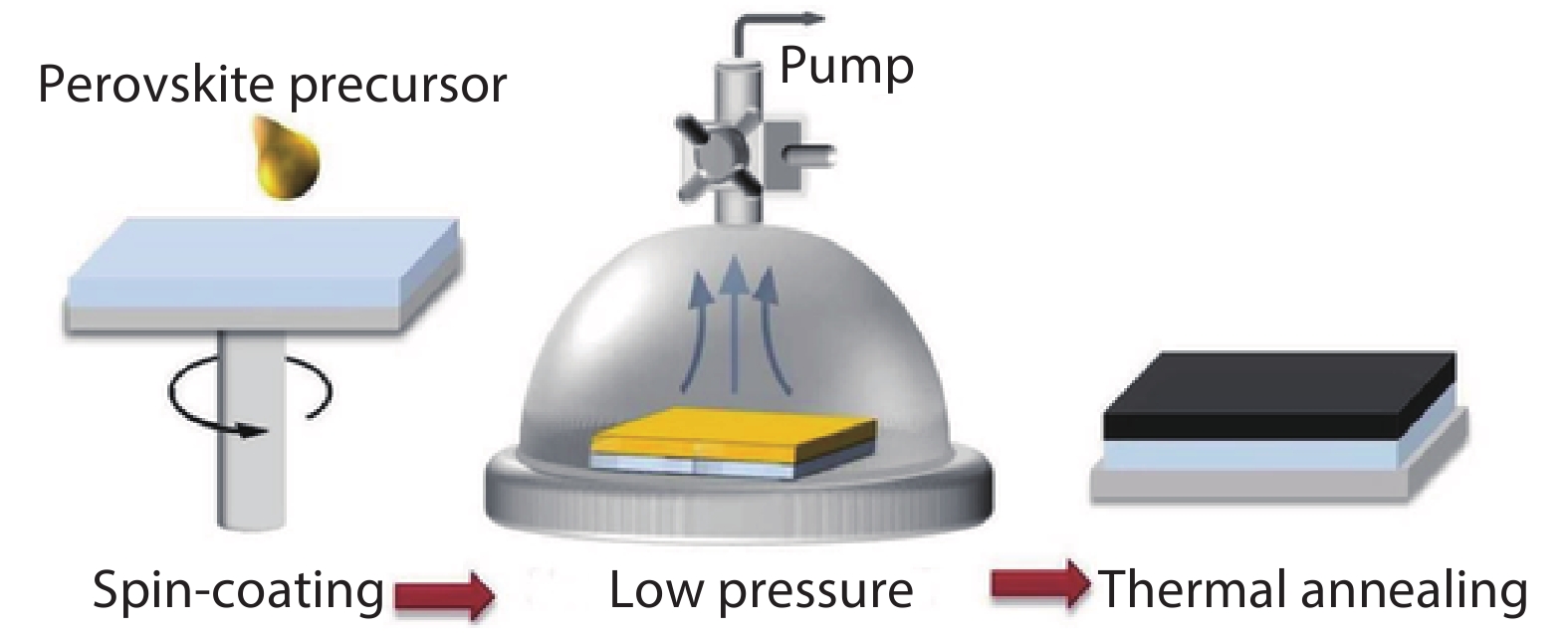
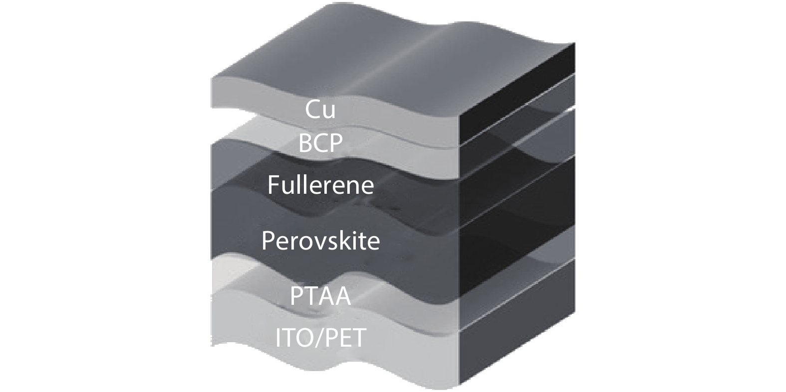
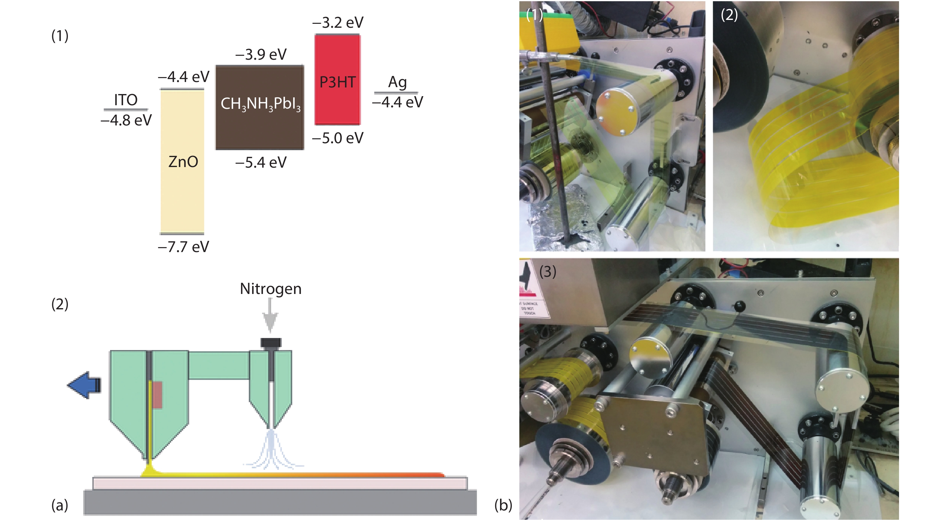
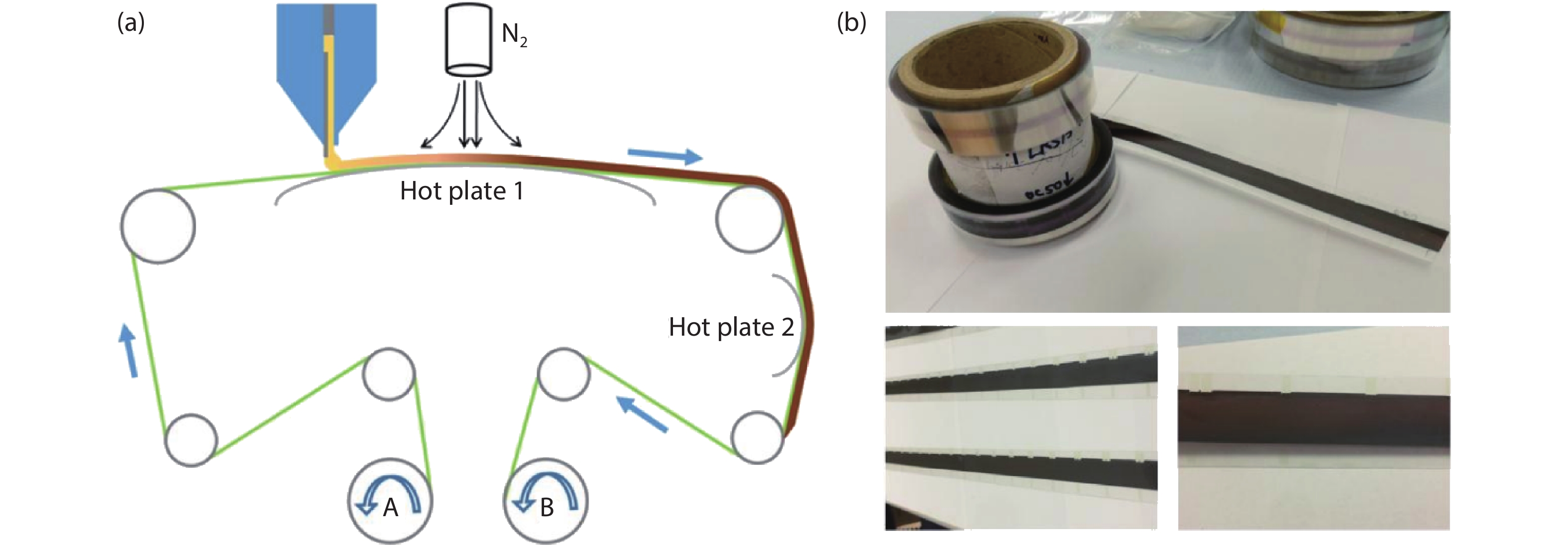
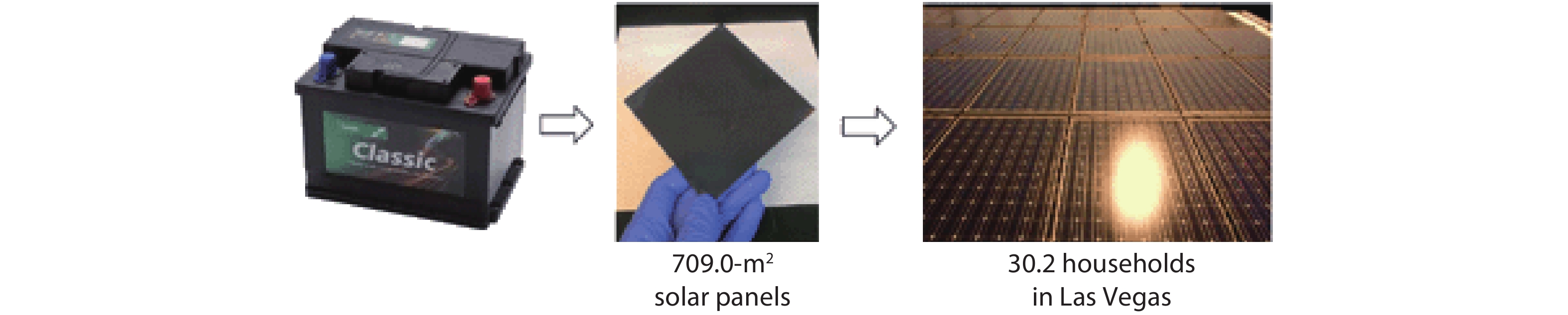
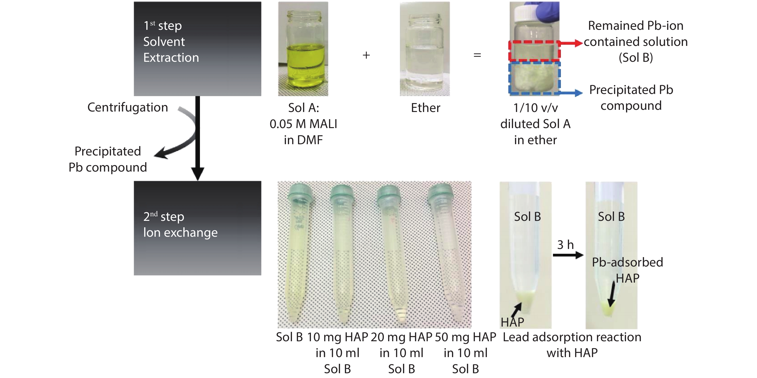
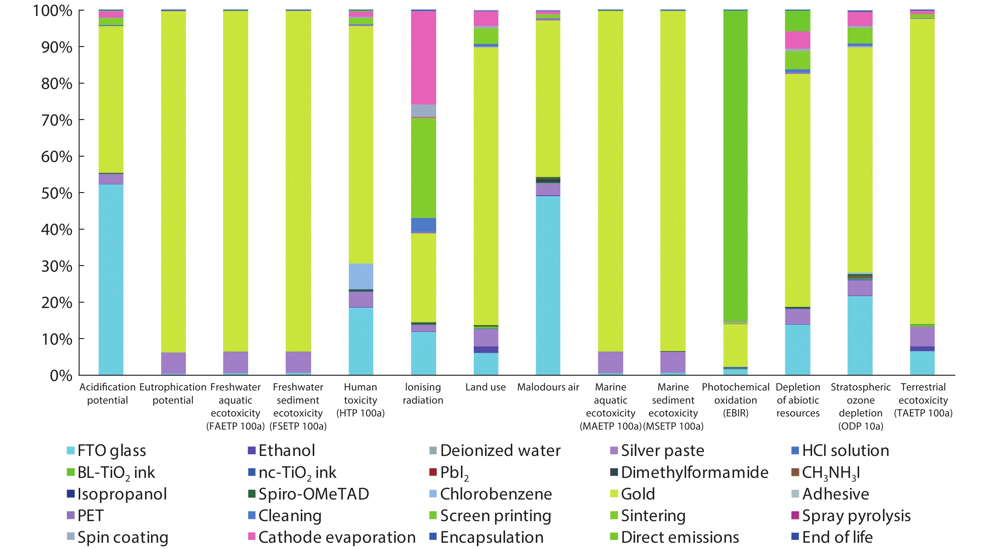
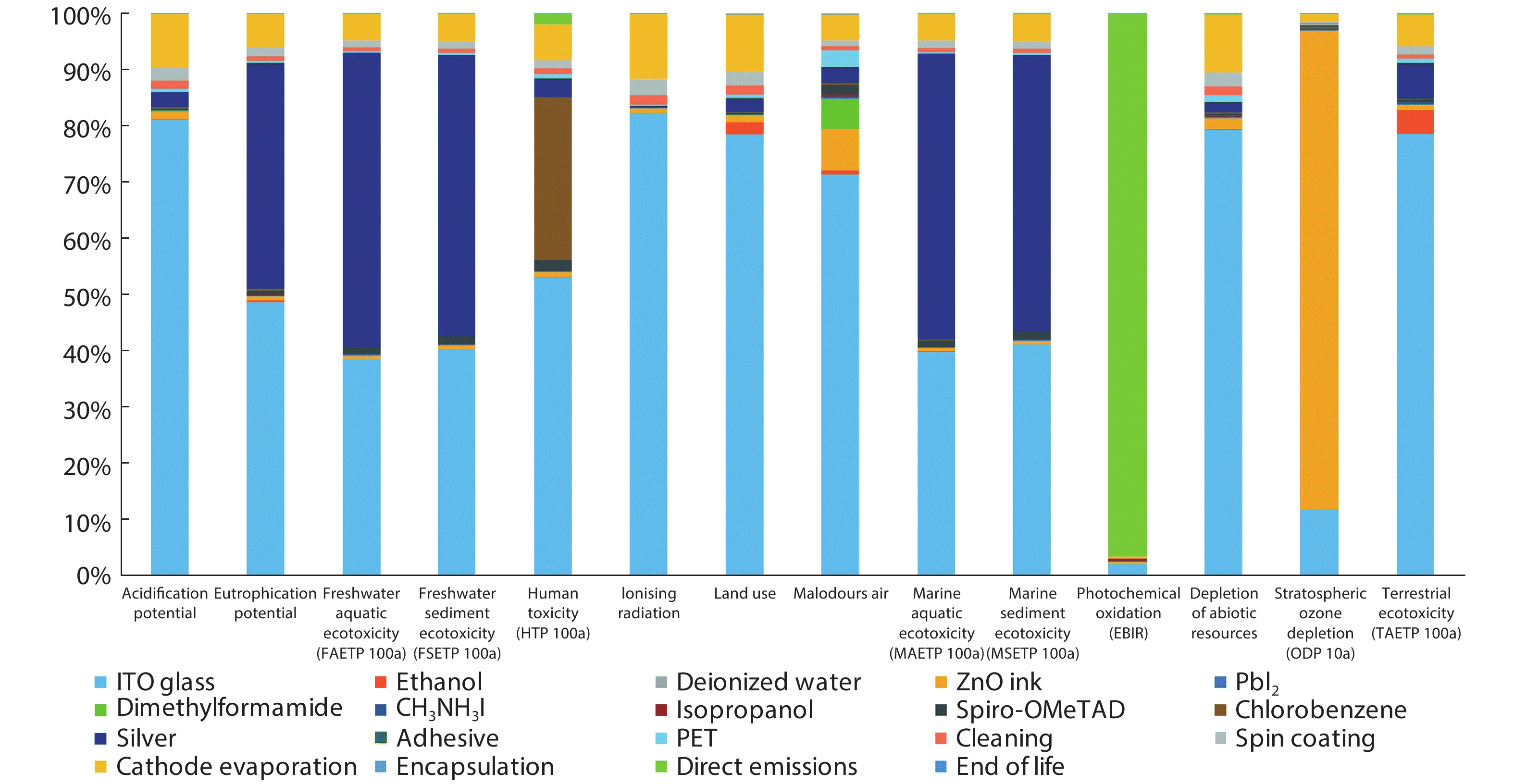
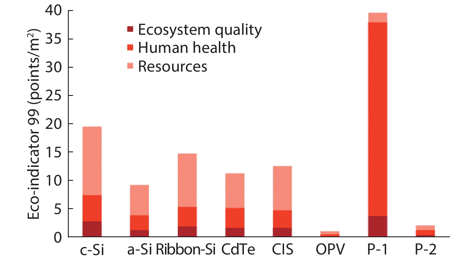
The perovskite material has many superb qualities which allow for its remarkable success as solar cells; flexibility is an emerging field for this technology. To encourage commercialization of flexible perovskite solar cells, two main areas are of focus: mitigation of stability issues and adaptation of production to flexible substrates. An in-depth report on stability concerns and solutions follows with a focus on Ruddlesden-Popper perovskites. Roll to roll processing of devices is desired to further reduce costs, so a review of flexible devices and their production methods follows as well. The final focus is on the sustainability of perovskite solar cell devices where recycling methods and holistic environmental impacts of devices are done.

J. Semicond.
2020, 41(4): 041604 doi: 10.1088/1674-4926/41/4/041604
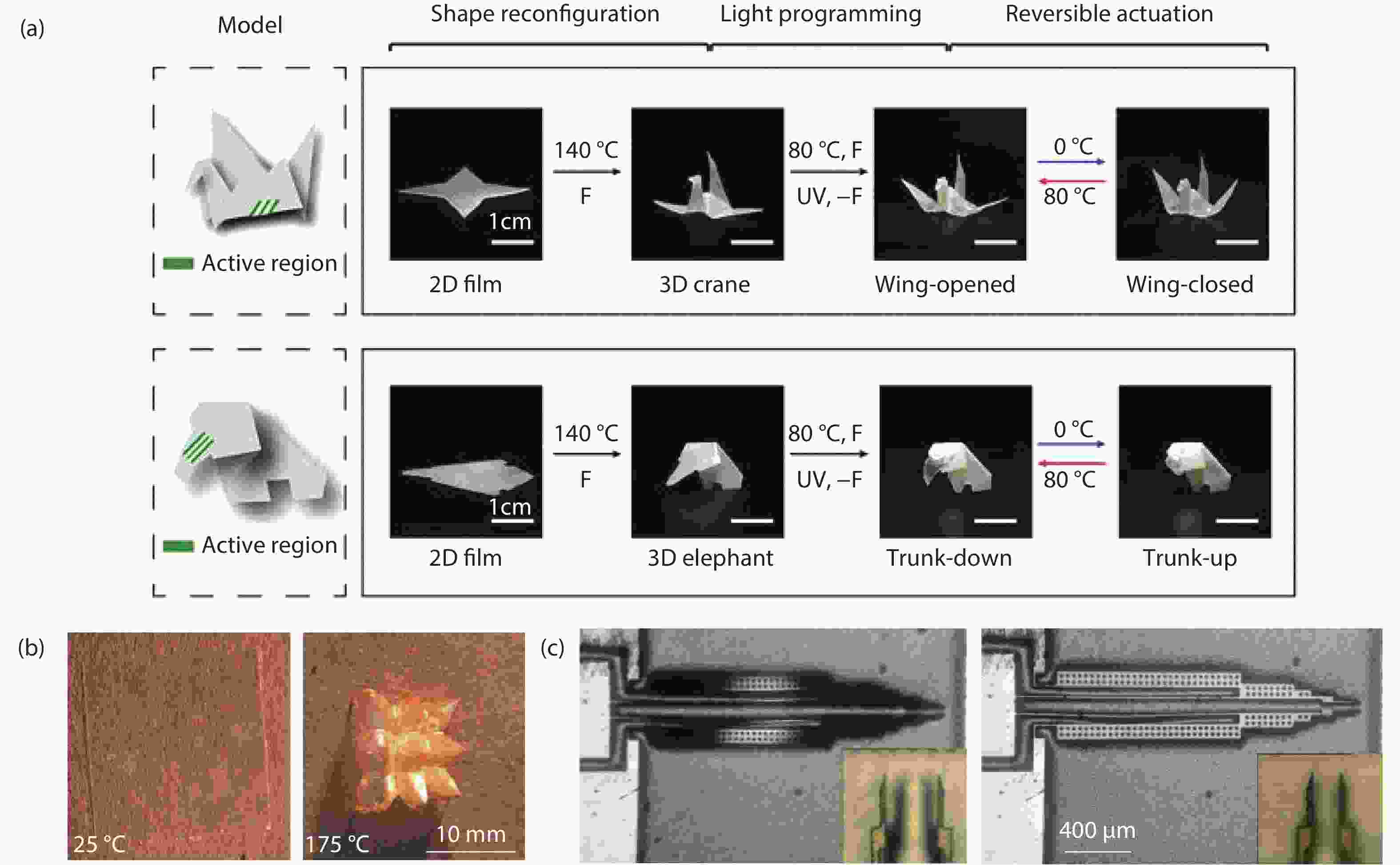
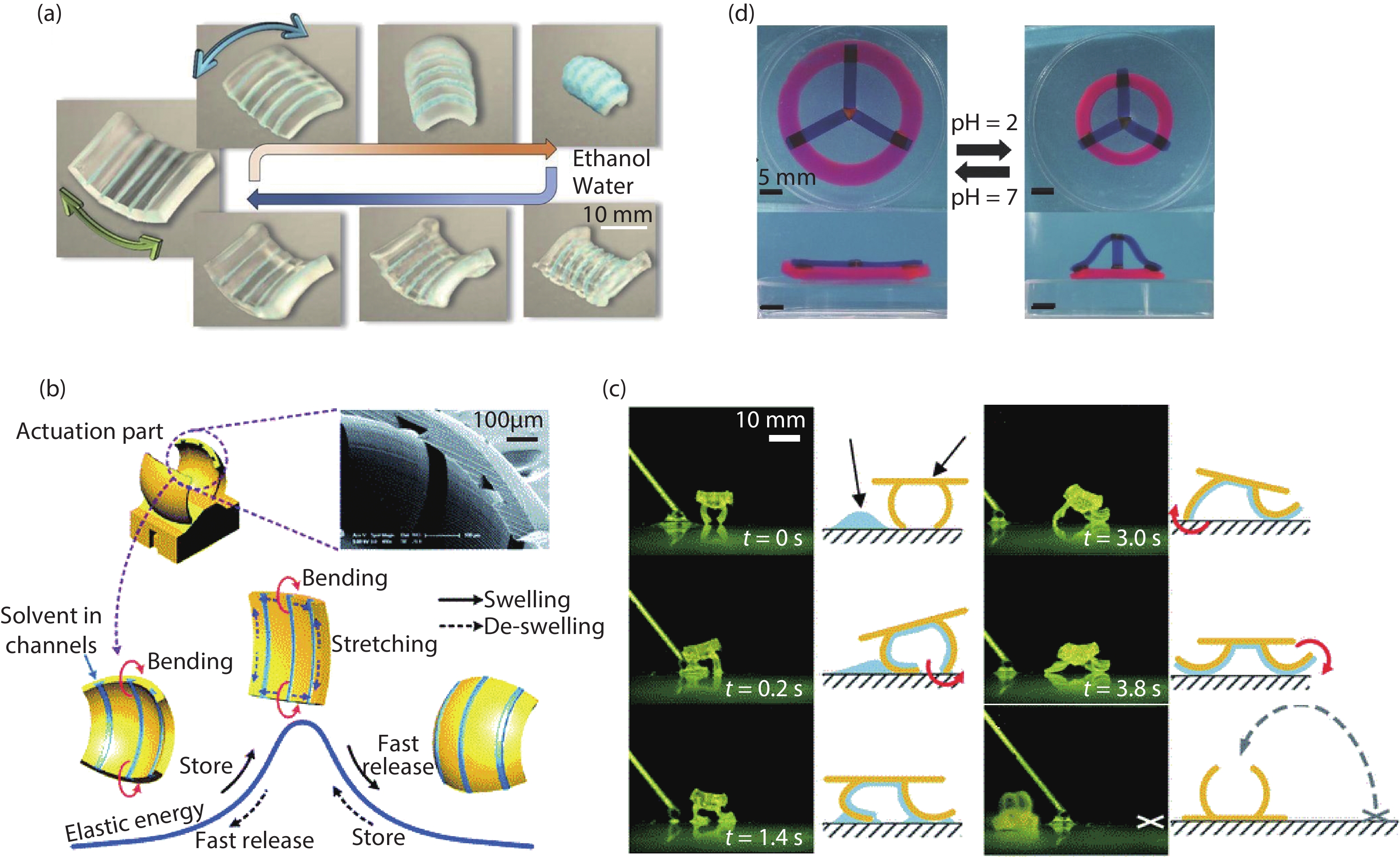
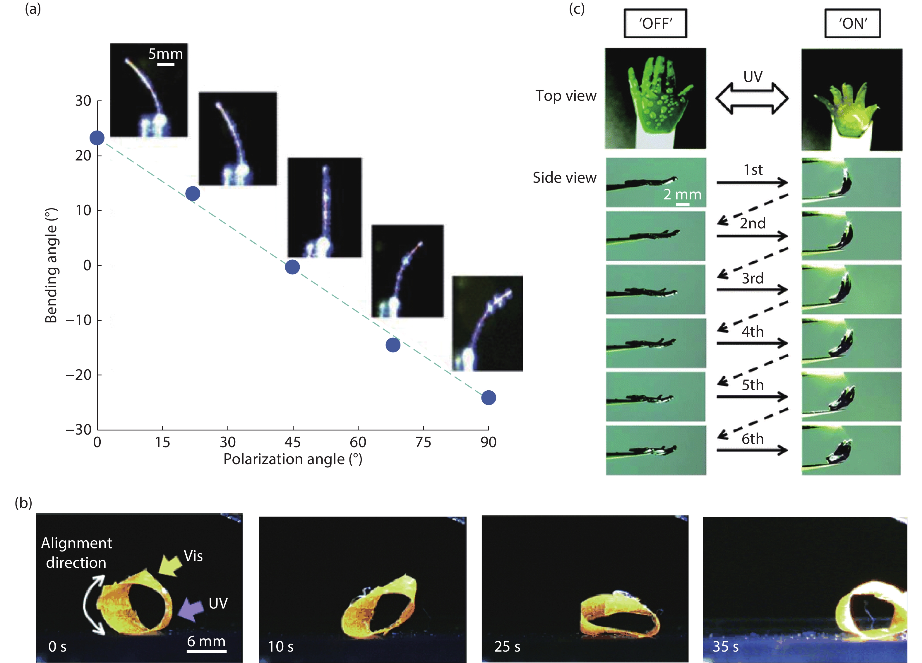
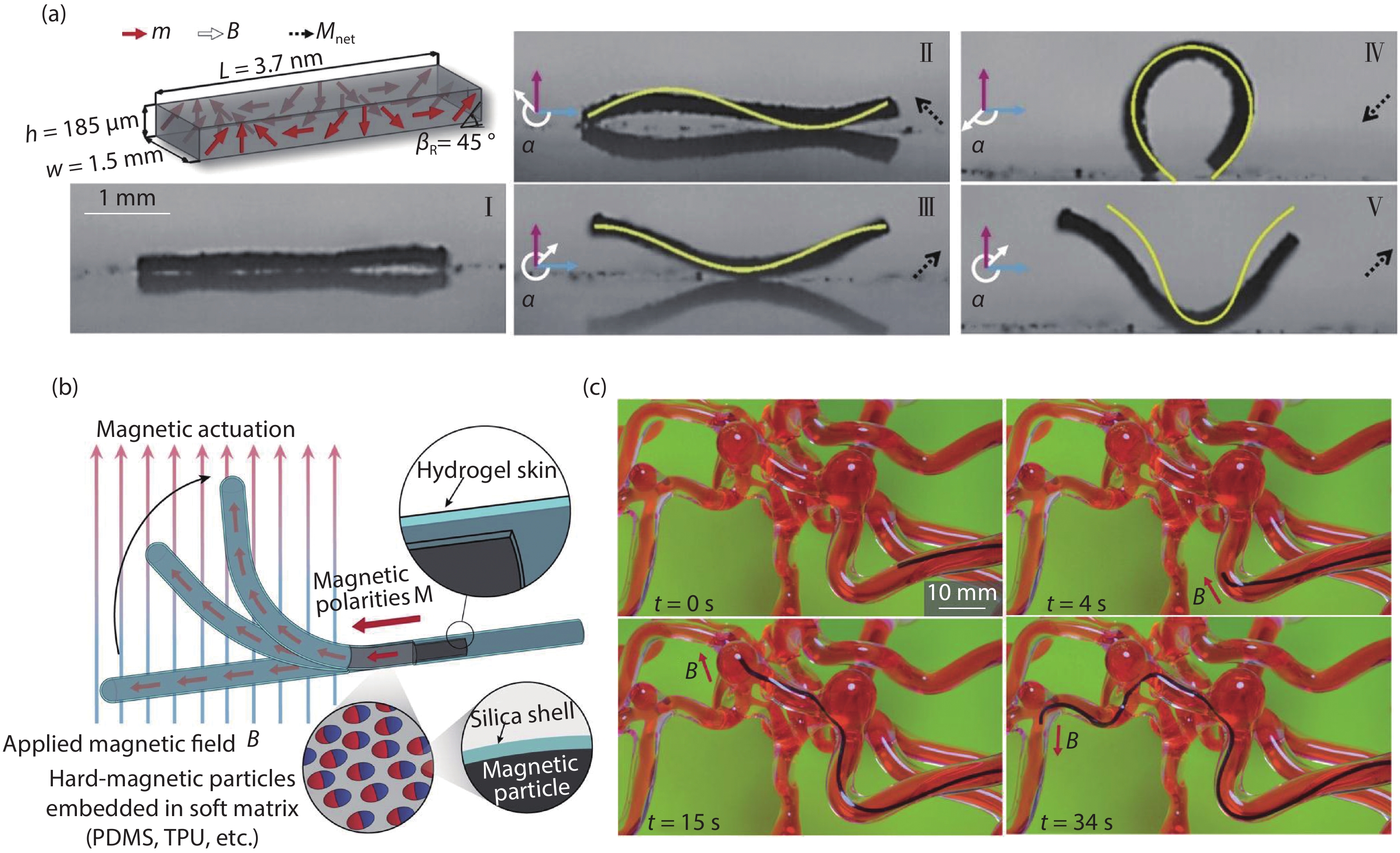
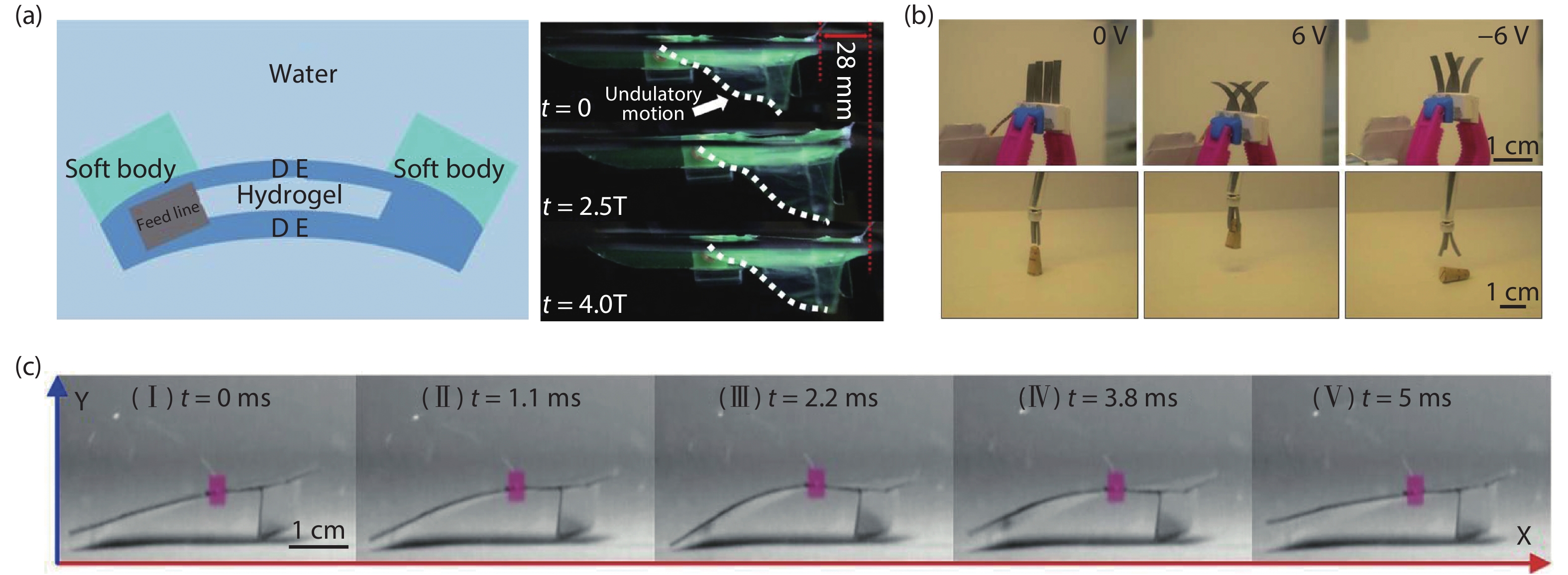
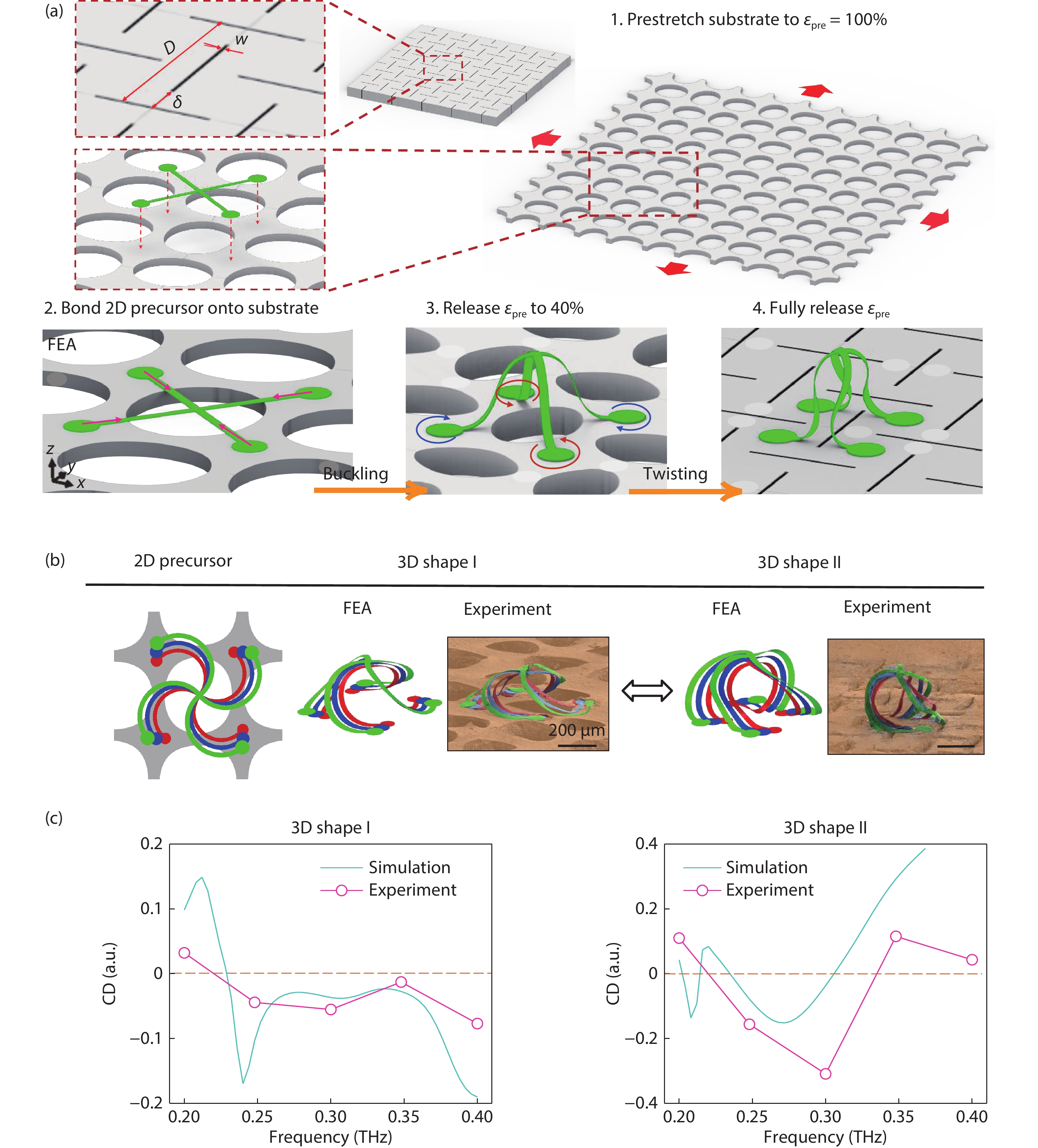
Soft robots complement the existing efforts of miniaturizing conventional, rigid robots, and have the potential to revolutionize areas such as military equipment and biomedical devices. This type of system can accomplish tasks in complex and time-varying environments through geometric reconfiguration induced by diverse external stimuli, such as heat, solvent, light, electric field, magnetic field, and mechanical field. Approaches to achieve reconfigurable mesostructures are essential to the design and fabrication of soft robots. Existing studies mainly focus on four key aspects: reconfiguration mechanisms, fabrication schemes, deformation control principles, and practical applications. This review presents a detailed survey of methodologies for morphable mesostructures triggered by a wide range of stimuli, with a number of impressive examples, demonstrating high degrees of deformation complexities and varied multi-functionalities. The latest progress based on the development of new materials and unique design concepts is highlighted. An outlook on the remaining challenges and open opportunities is provided.


J. Semicond.
2020, 41(4): 041605 doi: 10.1088/1674-4926/41/4/041605
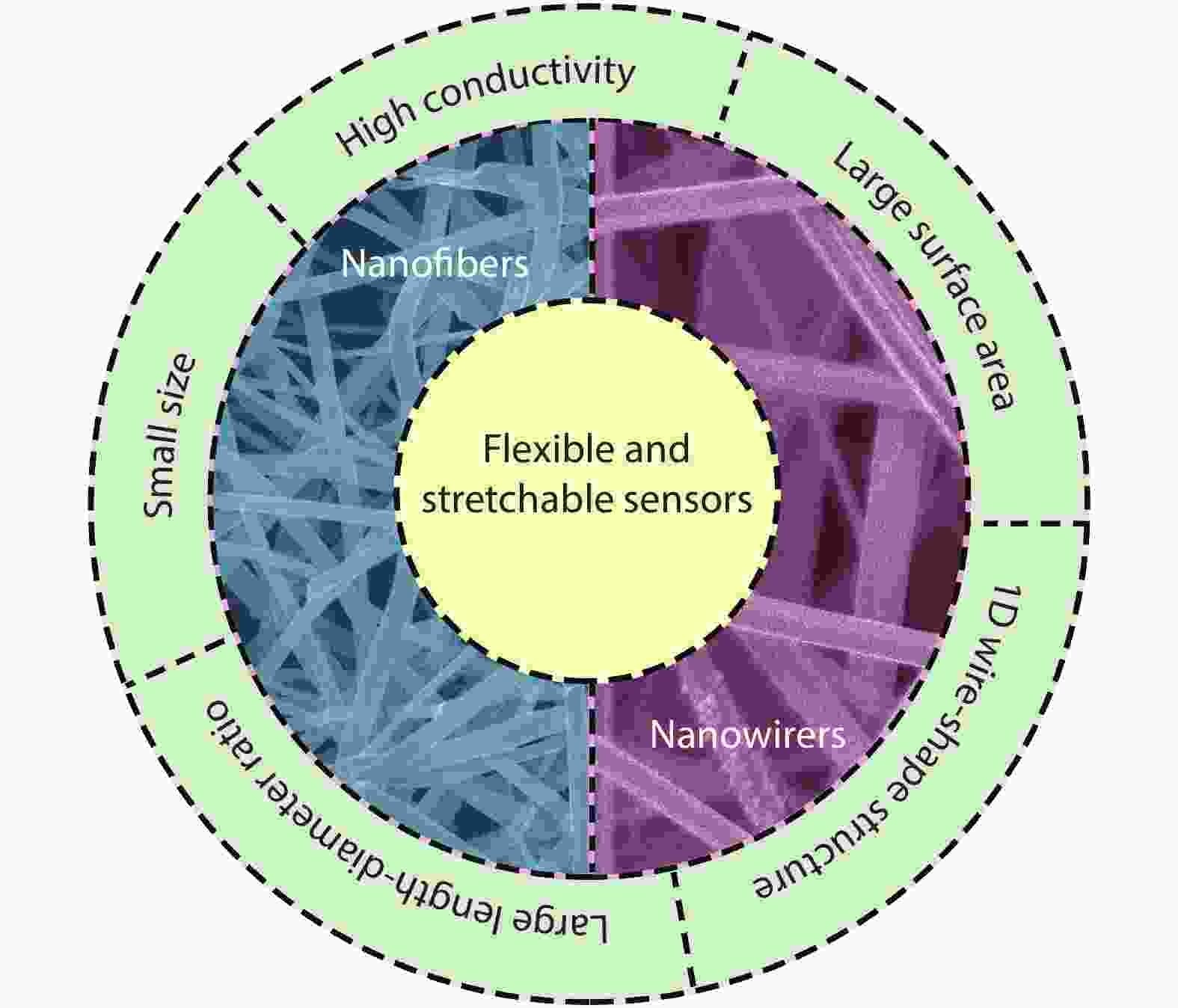
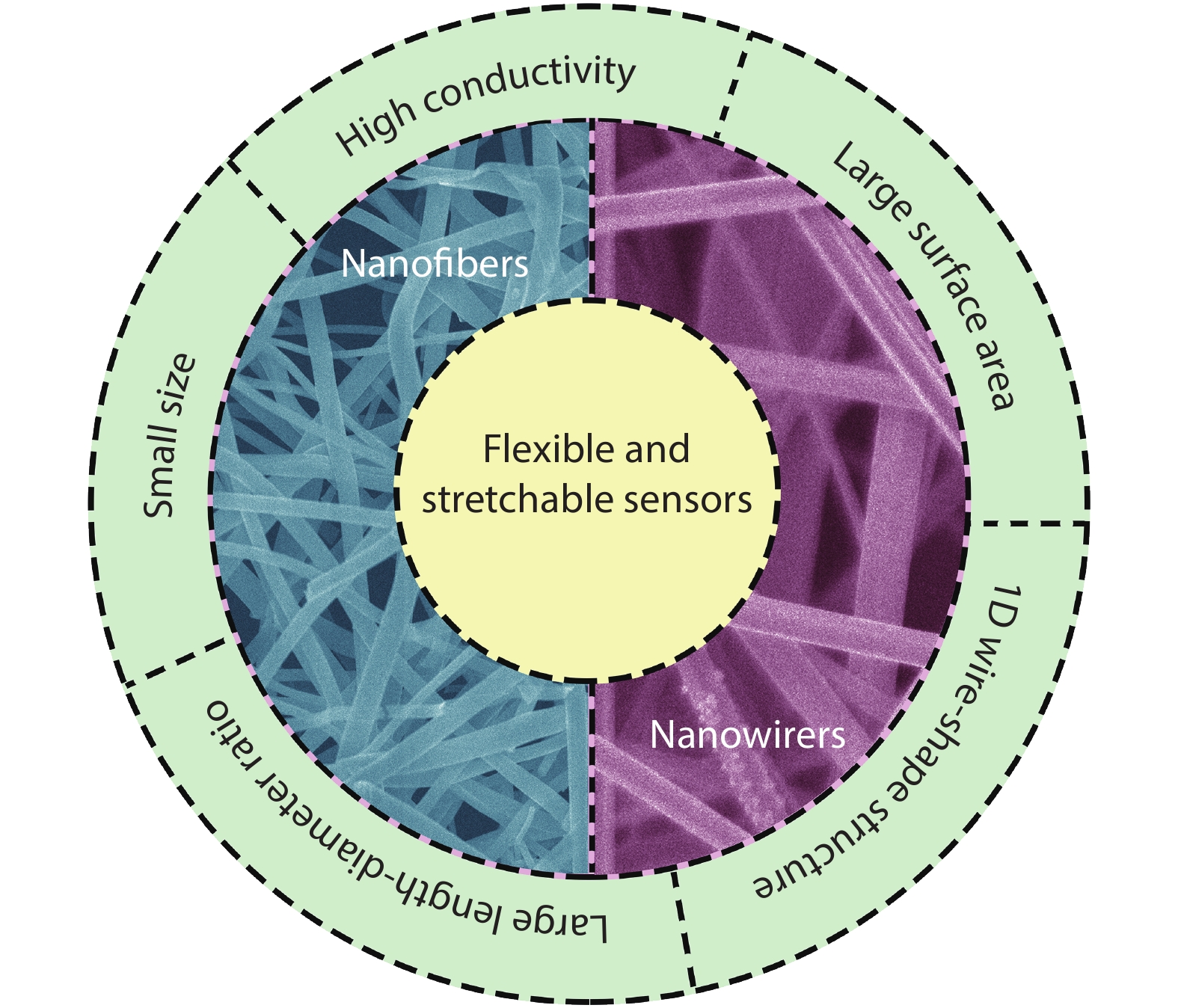
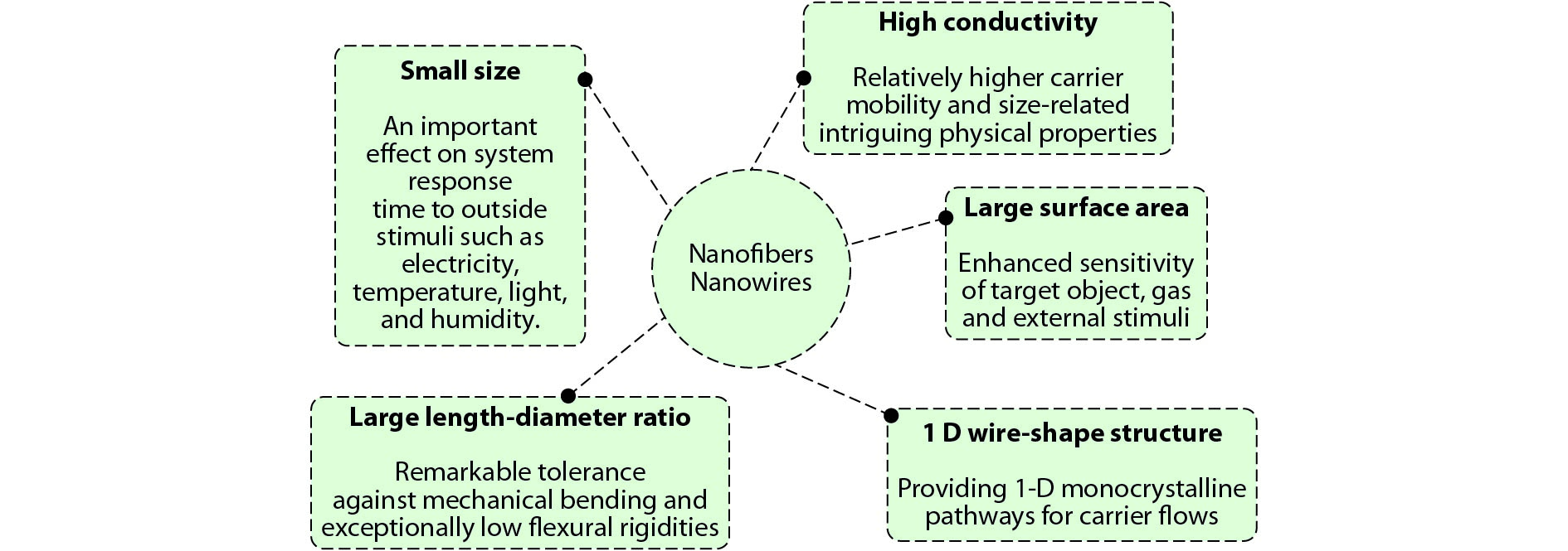
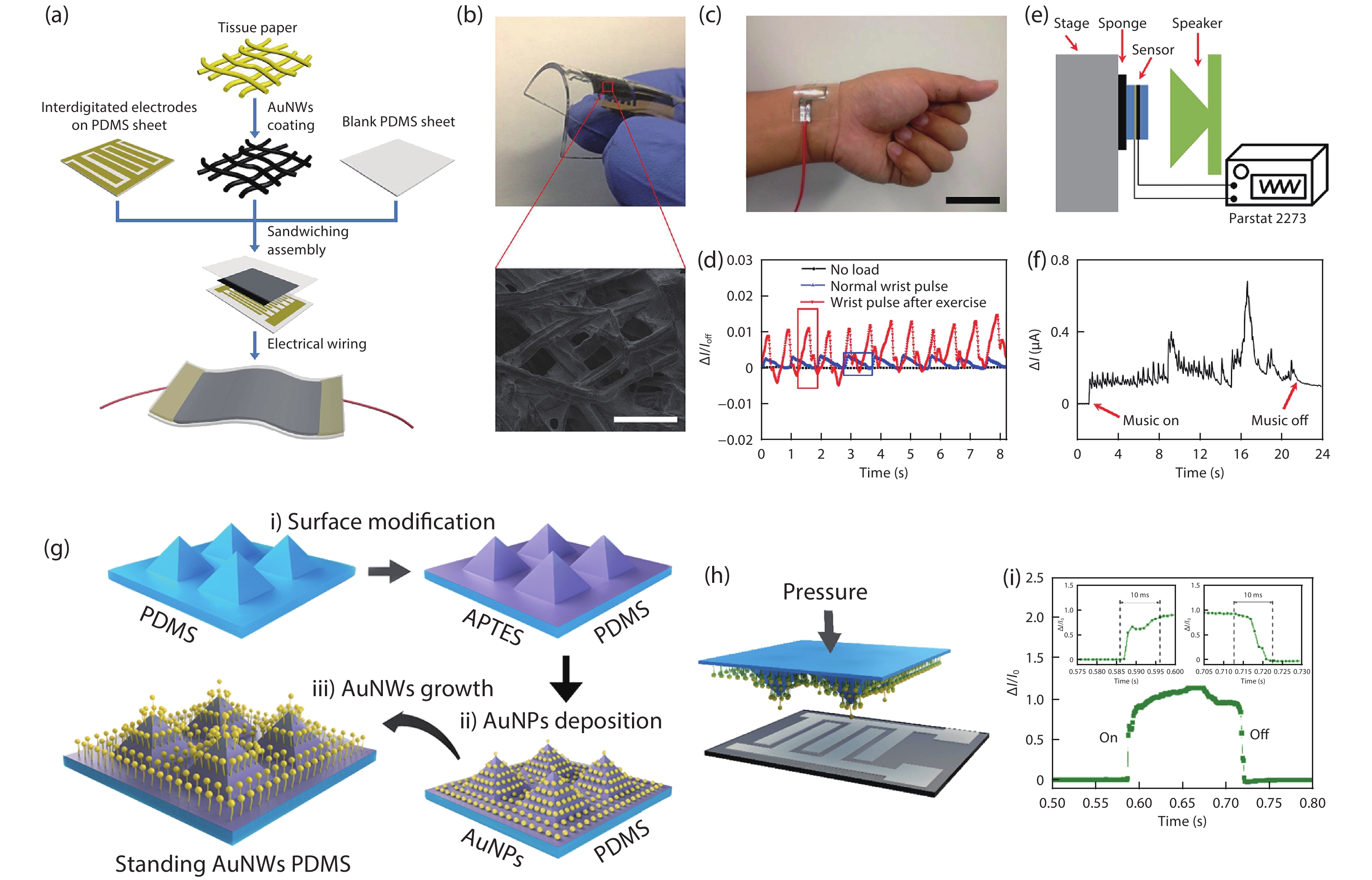
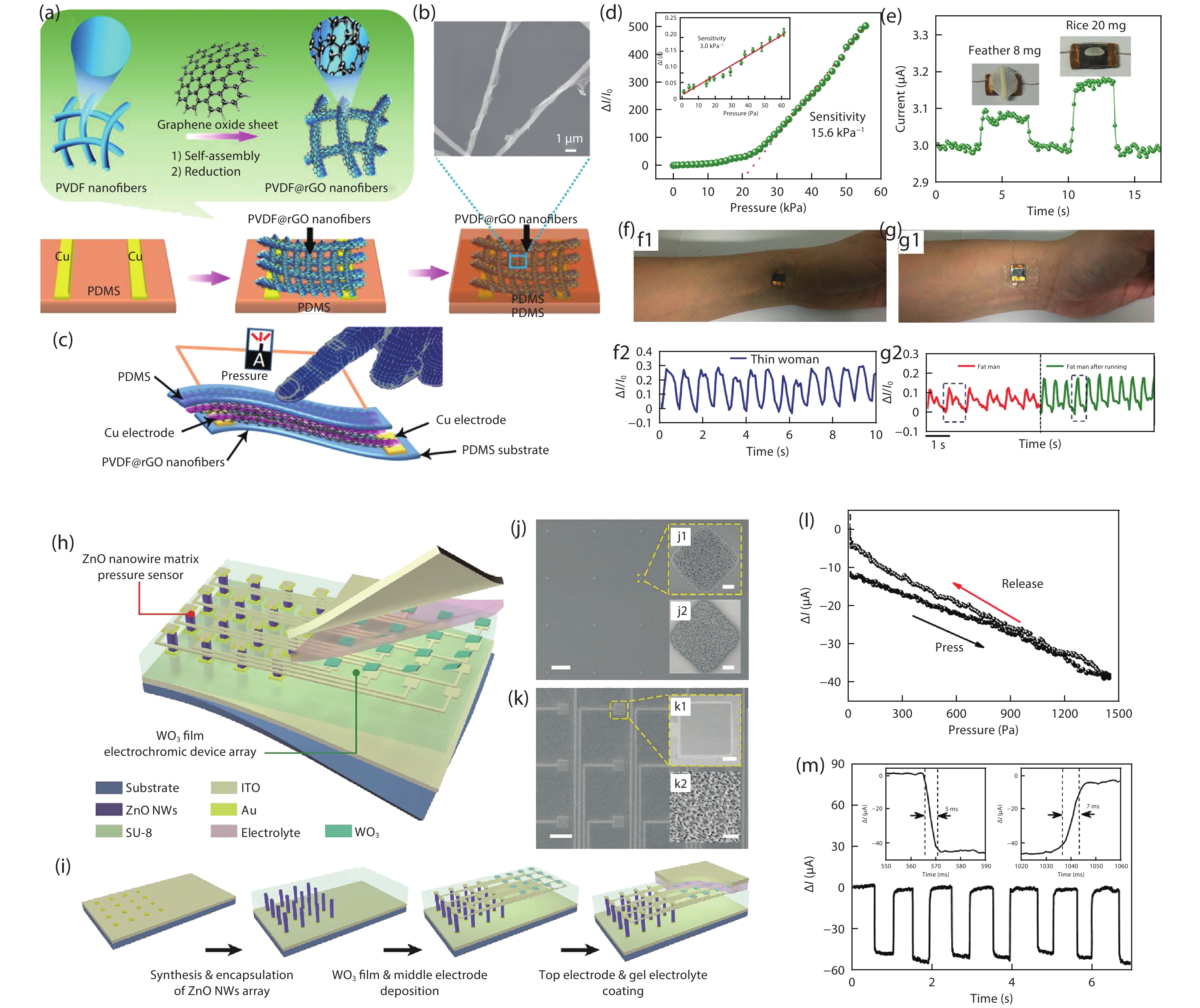
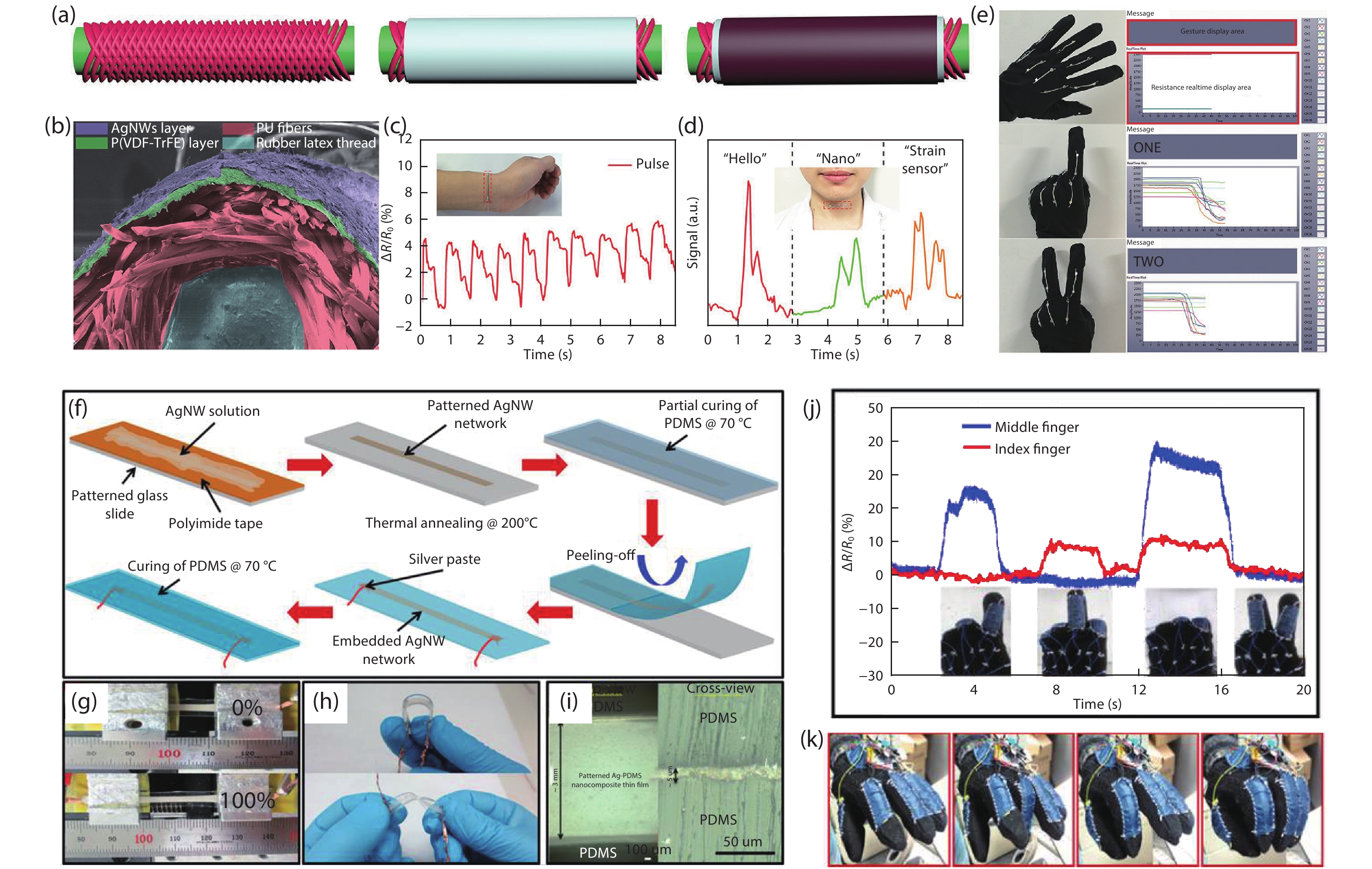
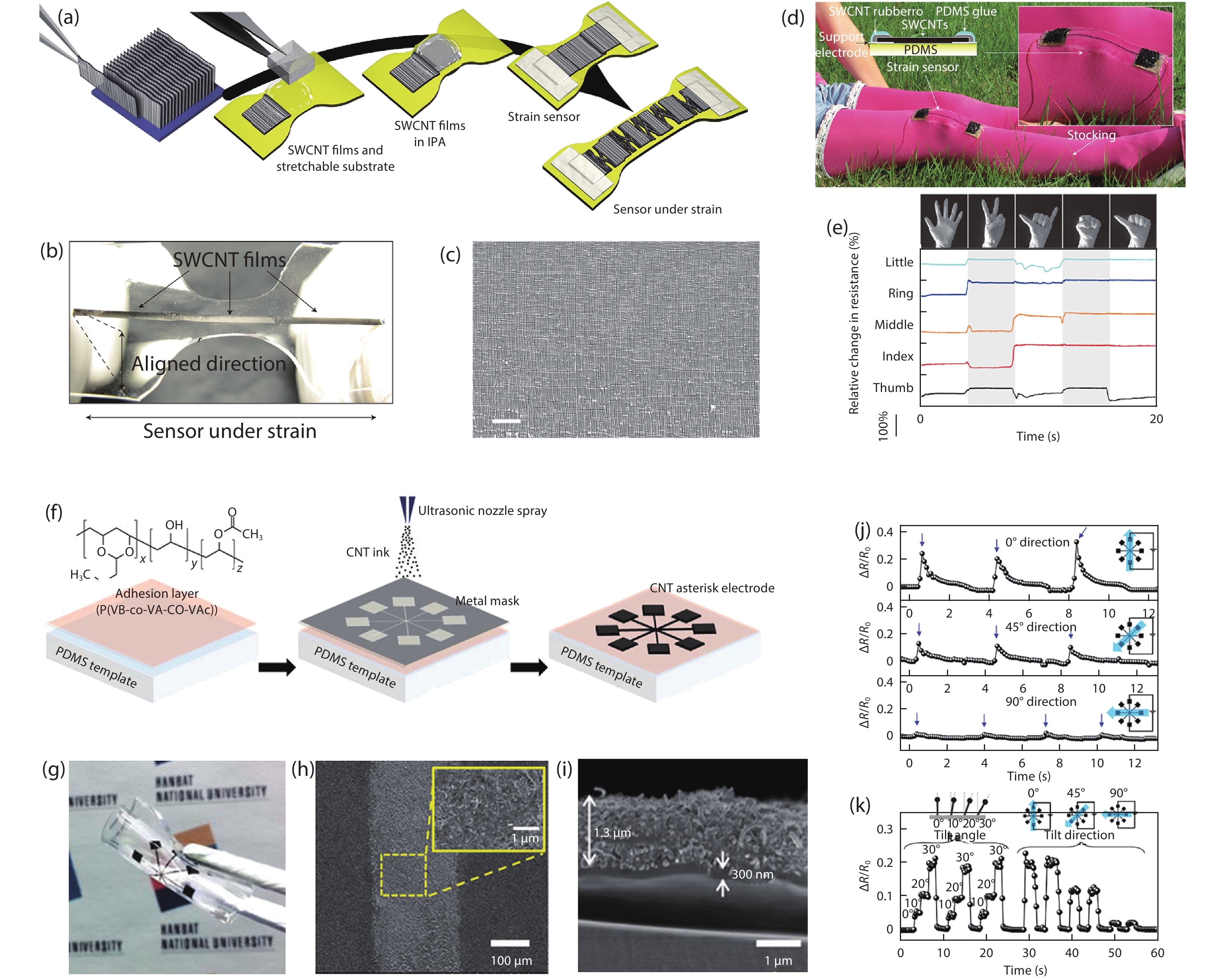
Nanofibers/nanowires with one-dimension (1D) nanostructure or well-patterned microstructure have shown distinctly advantages in flexible and stretchable sensor fields, owing to their remarkable tolerance against mechanical bending or stretching, outstanding electronic/optoelectronic properties, good transparency, and excellent geometry. Herein, latest summaries in the unique structure and properties of nanofiber/nanowire function materials and their applications for flexible and stretchable sensor are highlighted. Several types of high-performance nanofiber/nanowire-based flexible pressure and stretchable sensors are also reviewed. Finally, a conclusion and prospect for 1D nanofiber/nanowires-based flexible and stretchable sensors are also intensively discussed. This summary offers new insights for the development of flexible and stretchable sensor based 1D nanostructure in next-generation flexible electronics.
J. Semicond.
2020, 41(4): 041606 doi: 10.1088/1674-4926/41/4/041606
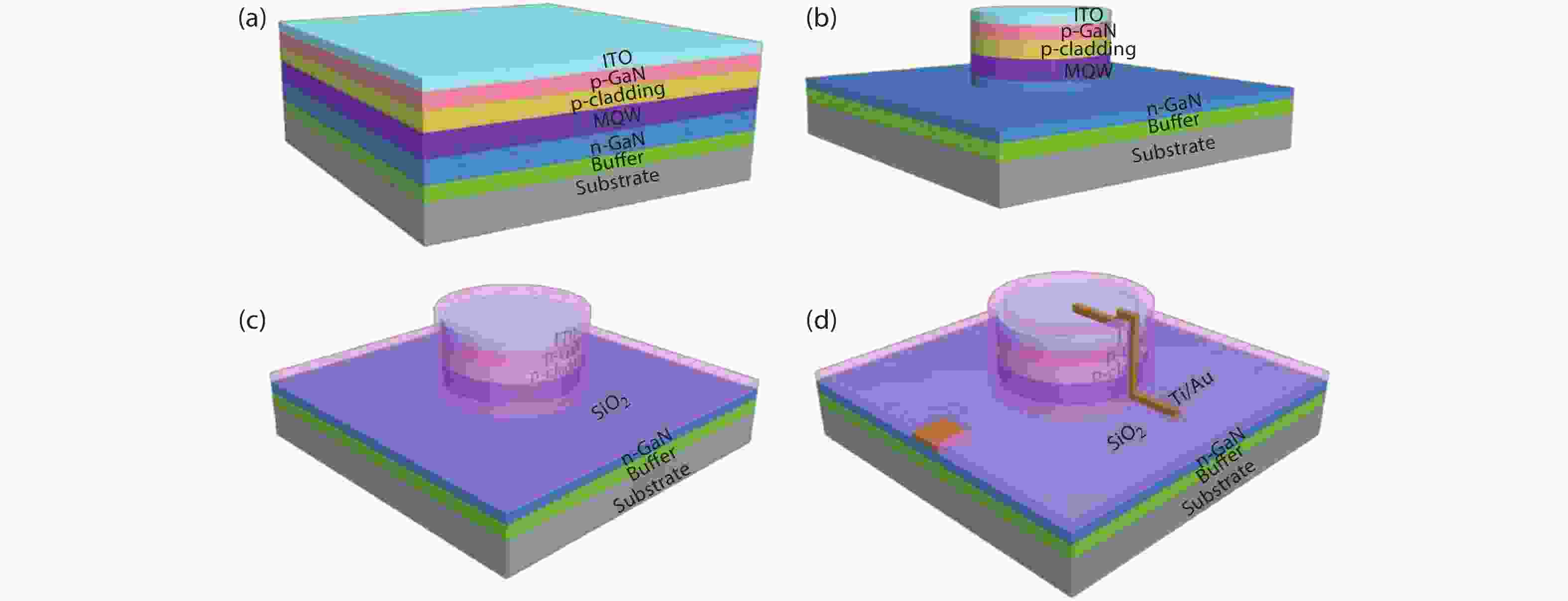
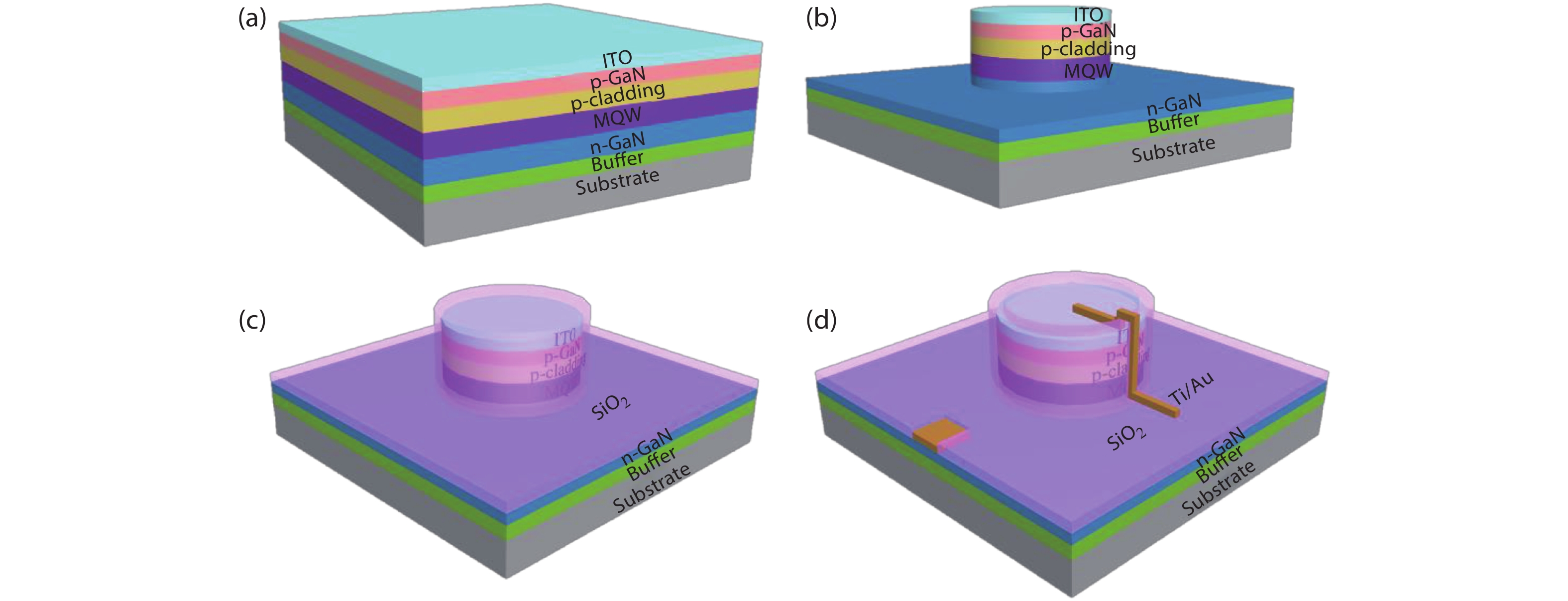
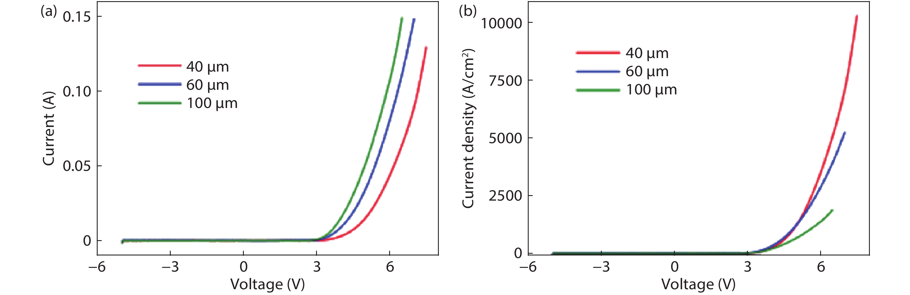
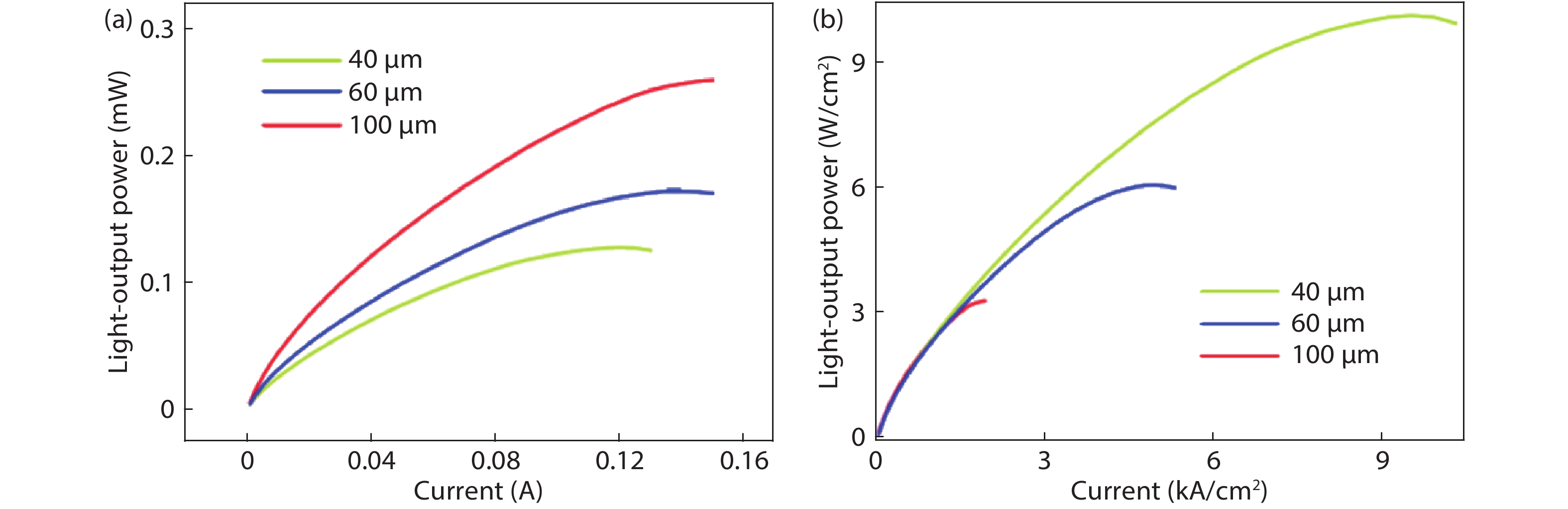
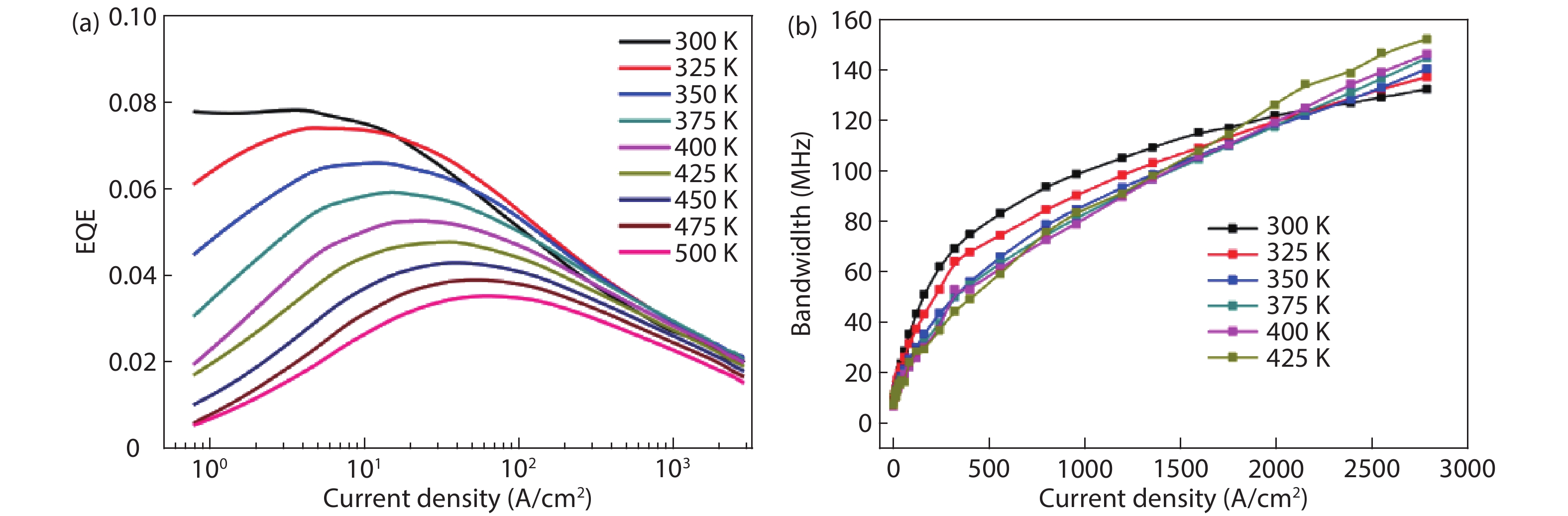
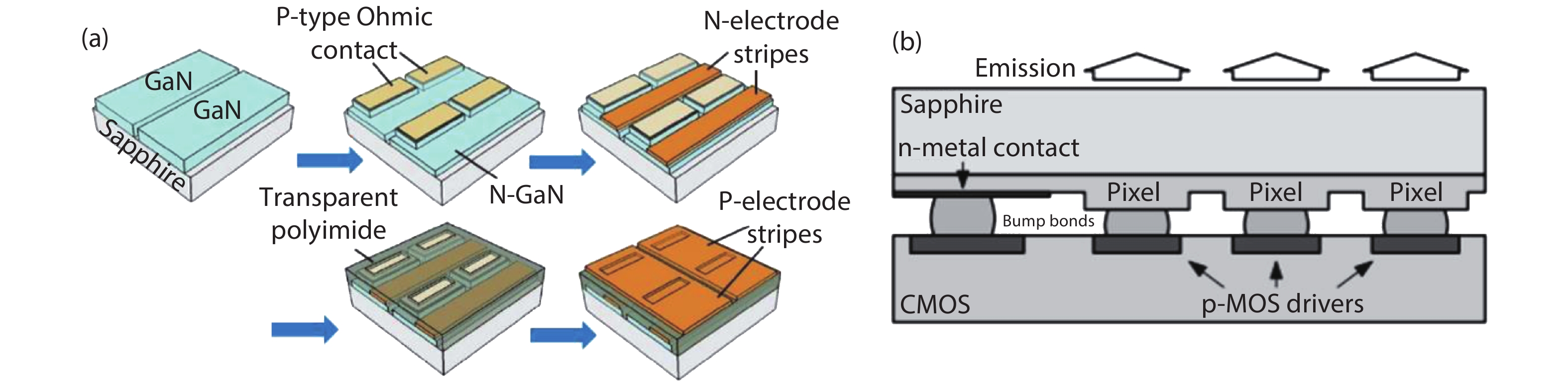
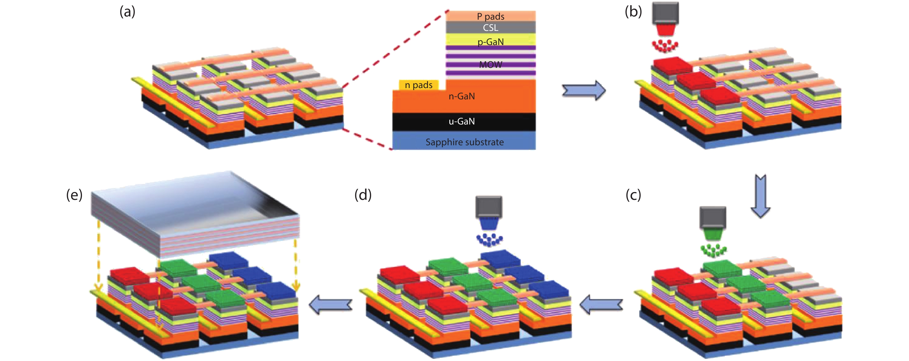
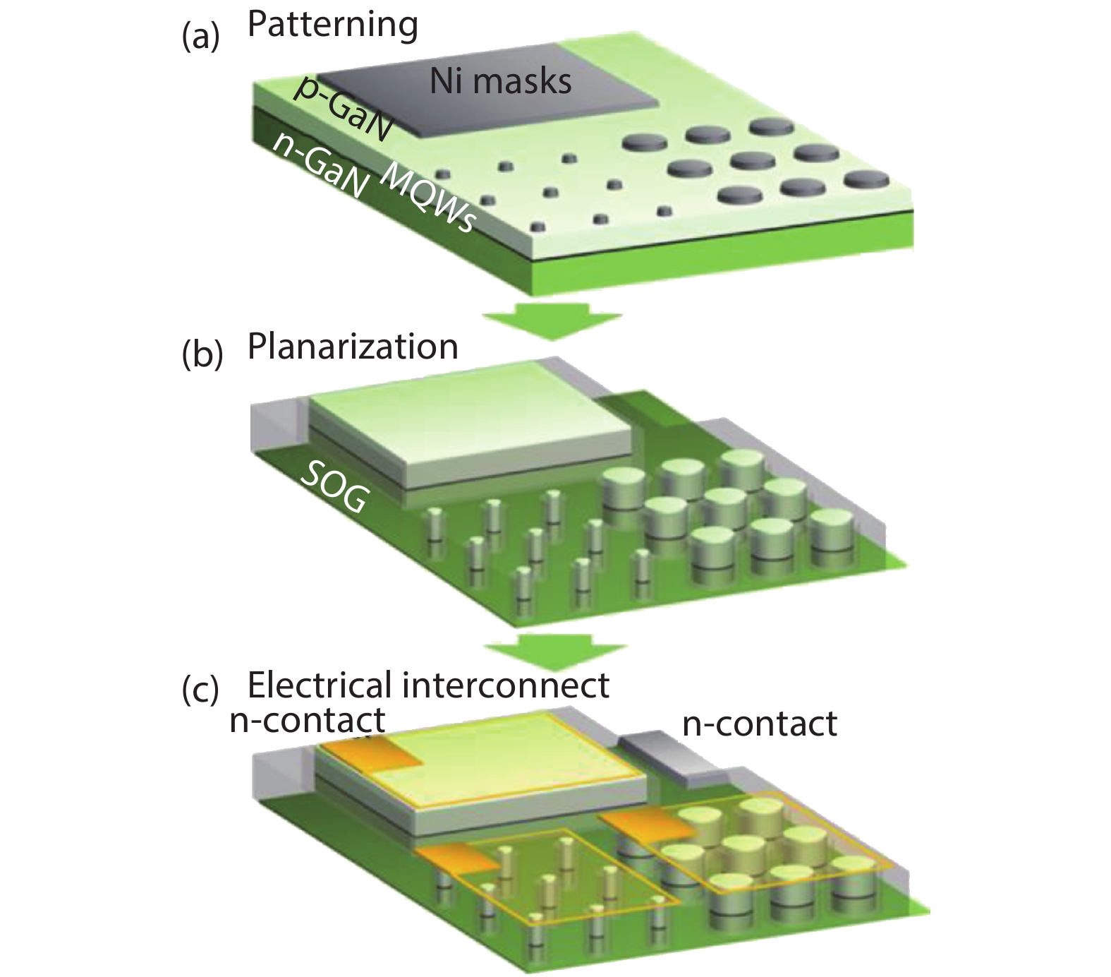
Due to the excellent optoelectronic properties, fast response time, outstanding power efficiency and high stability, micro-LED plays an increasingly important role in the new generation of display technology compared with LCD and OLED display. This paper mainly introduces the preparation methods of the GaN-based micro-LED array, the optoelectronic characteristics, and several key technologies to achieve full-color display, such as transfer printing, color conversion by quantum dot and local strain engineering.
J. Semicond.
2020, 41(4): 041607 doi: 10.1088/1674-4926/41/4/041607
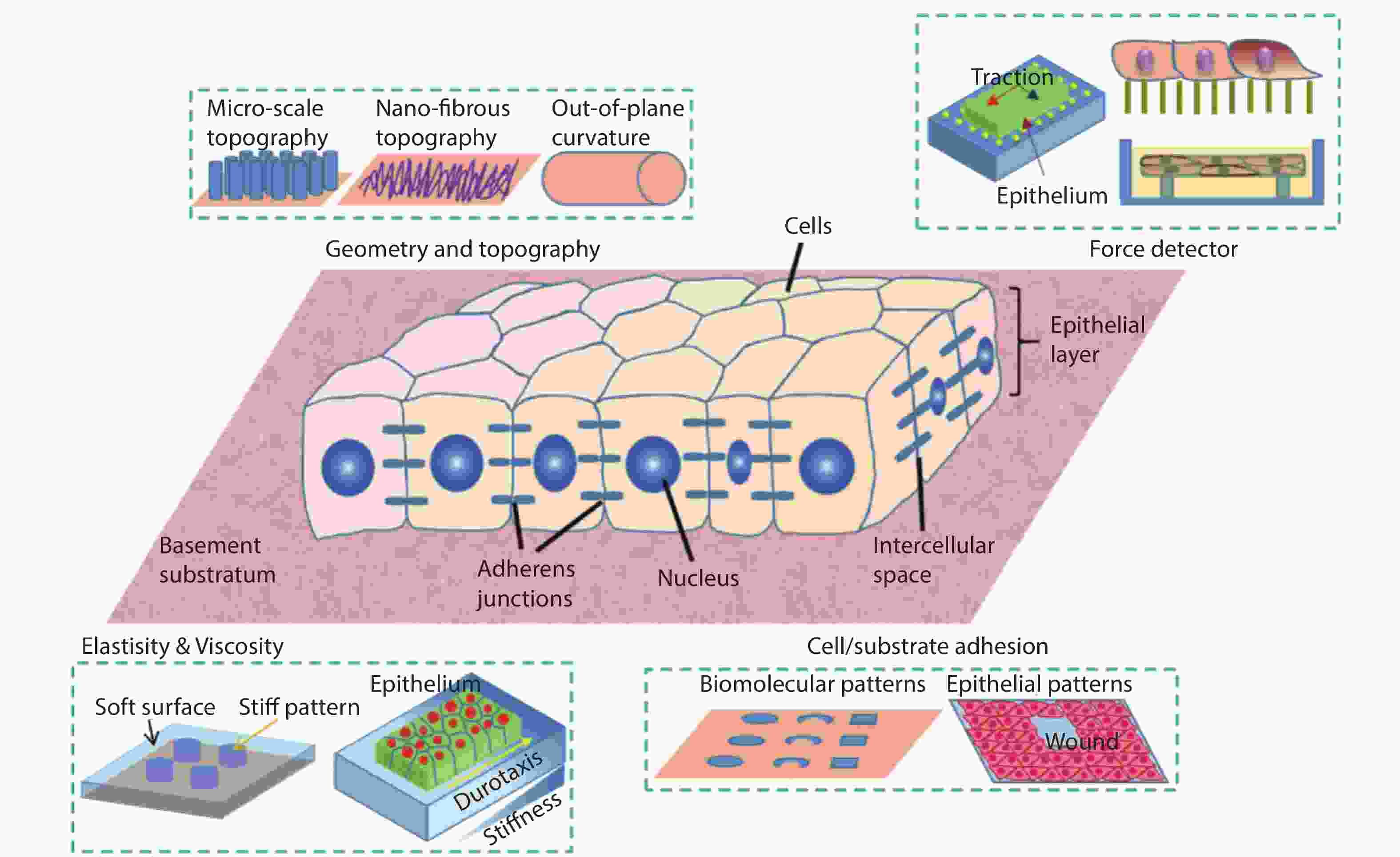
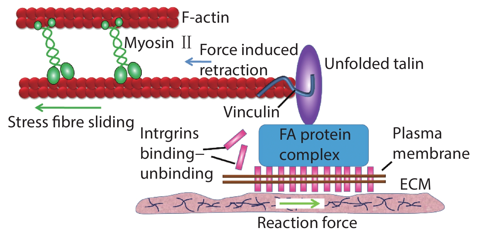
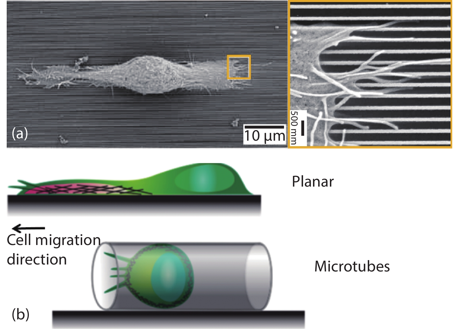
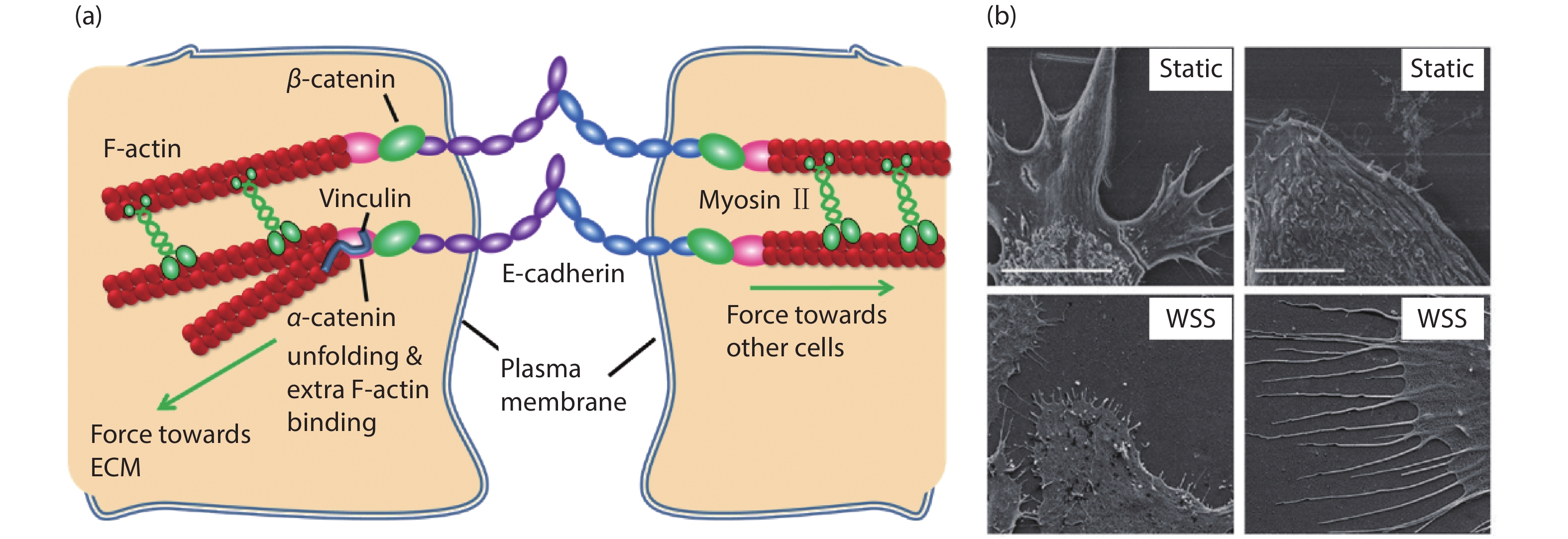
Both biological and engineering approaches have contributed significantly to the recent advance in the field of mechanobiology. Collaborating with biologists, bio-engineers and materials scientists have employed the techniques stemming from the conventional semiconductor industry to rebuild cellular milieus that mimic critical aspects of in vivo conditions and elicit cell/tissue responses in vitro. Such reductionist approaches have help to unveil important mechanosensing mechanism in both cellular and tissue level, including stem cell differentiation and proliferation, tissue expansion, wound healing, and cancer metastasis. In this mini-review, we discuss various microfabrication methods that have been applied to generate specific properties and functions of designer substrates/devices, which disclose cell-microenvironment interactions and the underlying biological mechanisms. In brief, we emphasize on the studies of cell/tissue mechanical responses to substrate adhesiveness, stiffness, topography, and shear flow. Moreover, we comment on the new concepts of measurement and paradigms for investigations of biological mechanotransductions that are yet to emerge due to on-going interdisciplinary efforts in the fields of mechanobiology and microengineering.


J. Semicond.
2020, 41(4): 042601 doi: 10.1088/1674-4926/41/4/042601

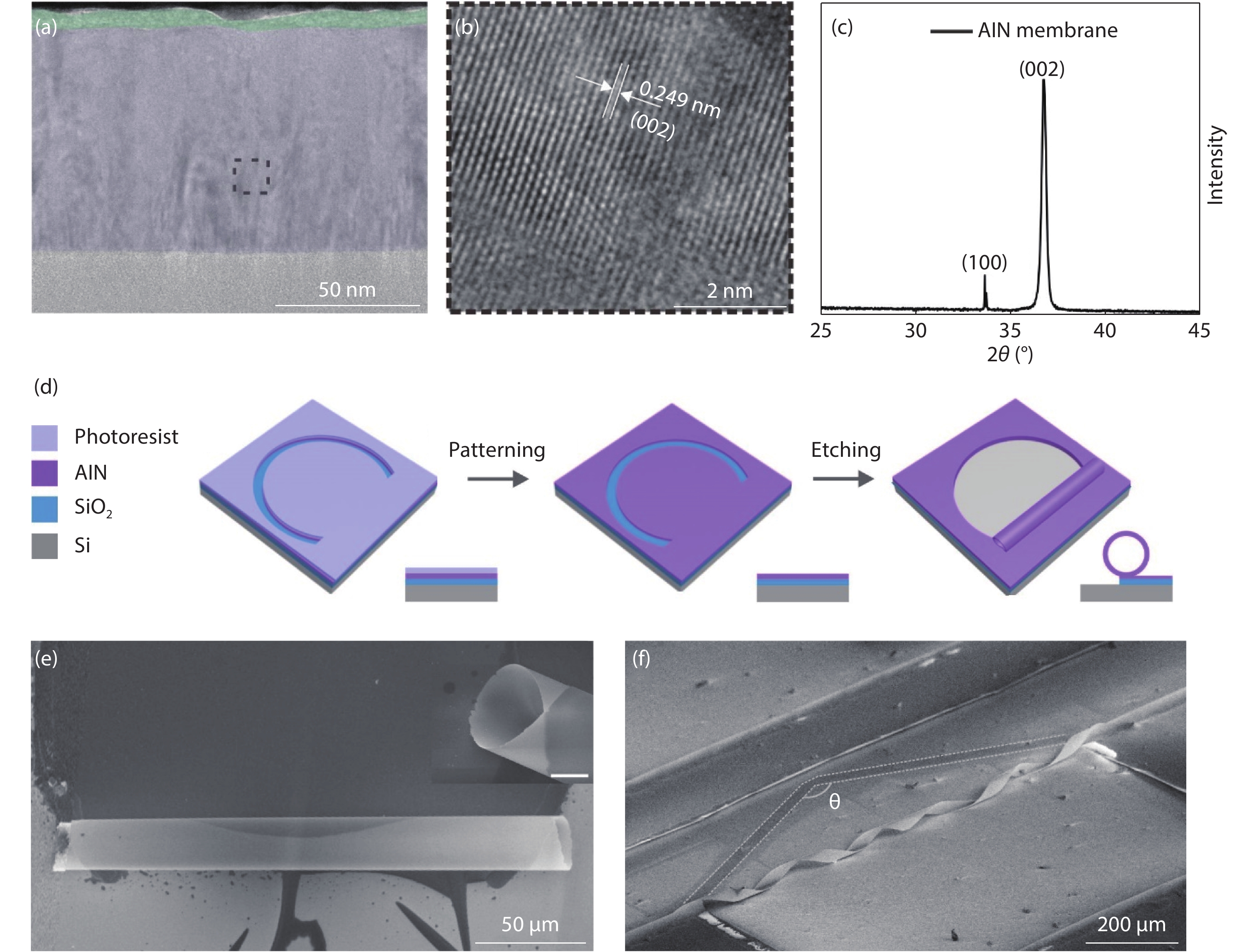
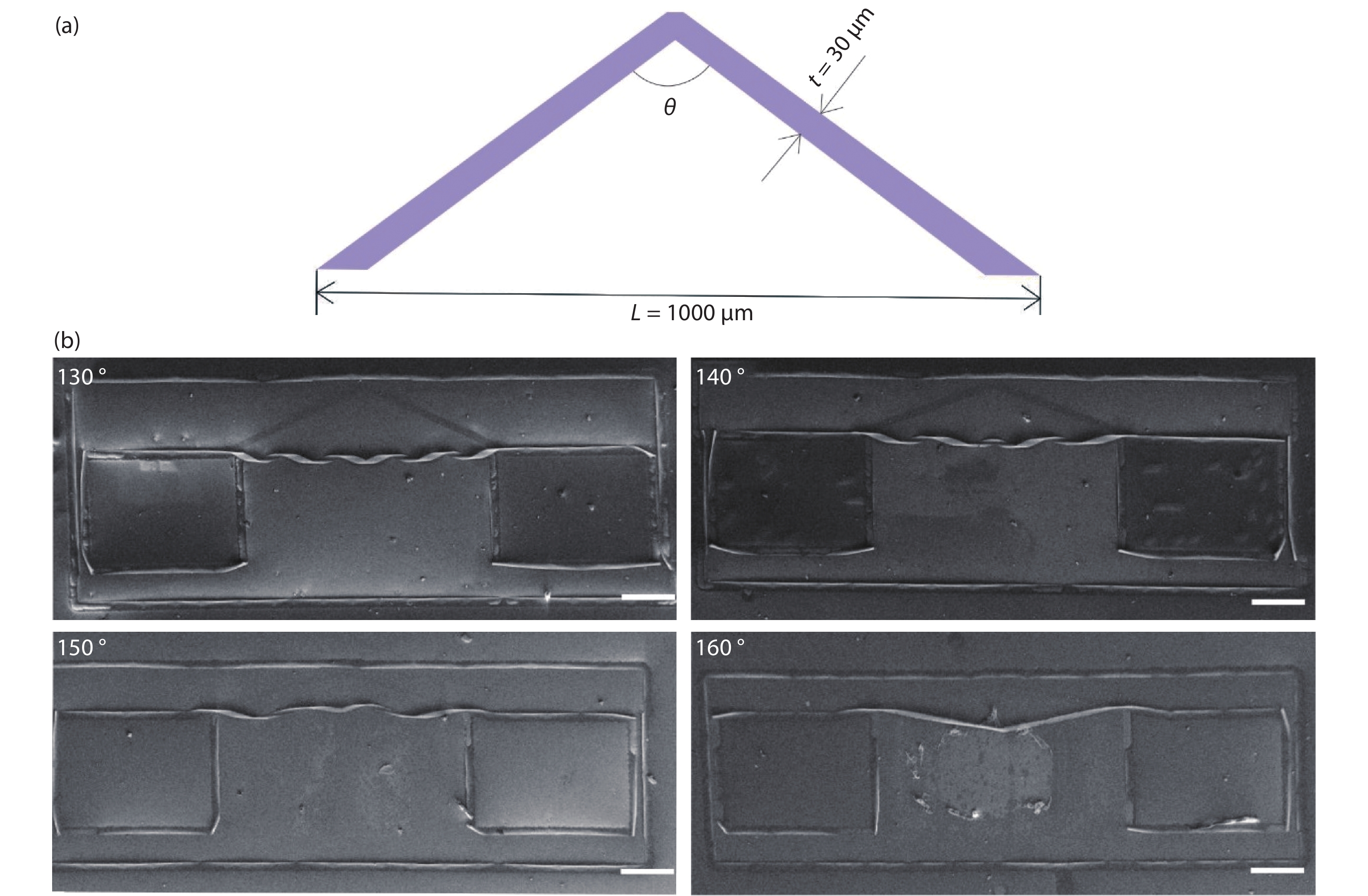
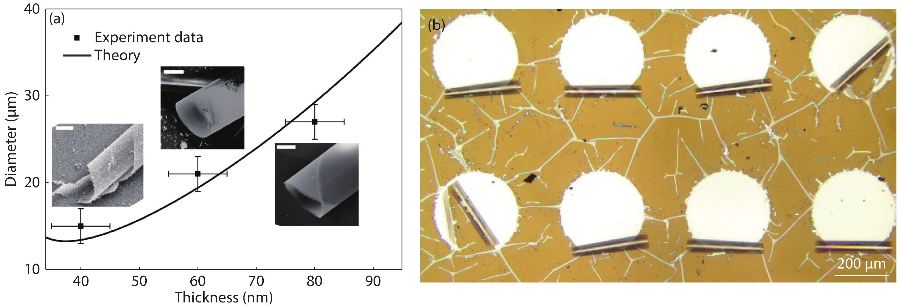
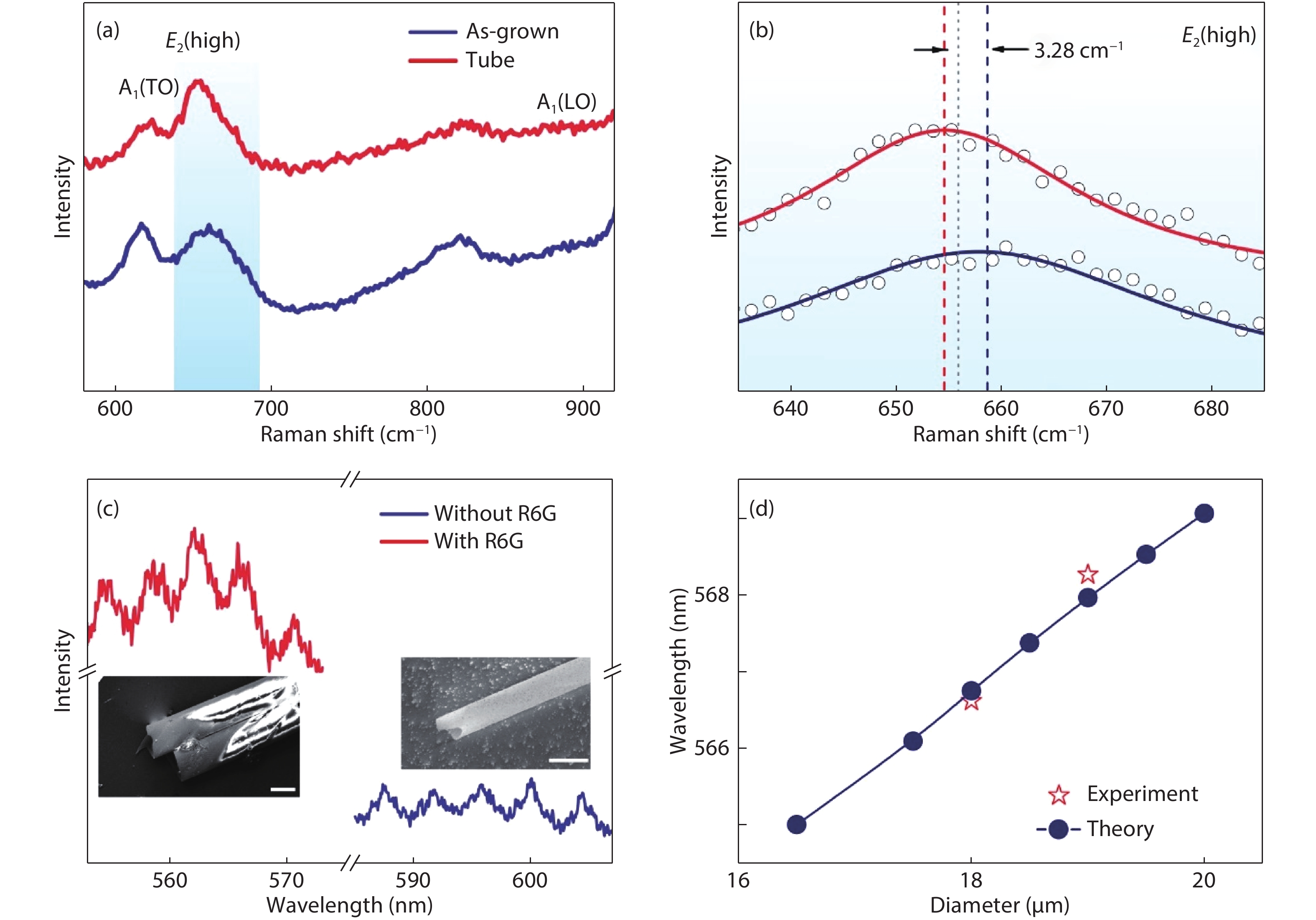
Aluminum nitride (AlN) has attracted a great amount of interest due to the fact that these group III–V semiconductors present direct band gap behavior and are compatible with current micro-electro-mechanical systems. In this work, three dimensional (3D) AlN architectures including tubes and helices were constructed by rolling up AlN nanomembranes grown on a silicon-on-insulator wafer via magnetron sputtering. The properties of the AlN membrane were characterized through transmission electron microscopy and X-ray diffraction. The thickness of AlN nanomembranes could be tuned via the RIE thinning method, and thus micro-tubes with different diameters were fabricated. The intrinsic strain in AlN membranes was investigated via micro-Raman spectroscopy, which agrees well with theory prediction. Whispering gallery mode was observed in AlN tubular optical microcavity in photoluminescence spectrum. A postprocess involving atomic layer deposition and R6G immersion were employed on as-fabricated AlN tubes to promote the Q-factor. The AlN tubular micro-resonators could offer a novel design route for Si-based integrated light sources. In addition, the rolled-up technology paves a new way for AlN 3D structure fabrication, which is promising for AlN application in MEMS and photonics fields.
J. Semicond.
2020, 41(4): 042602 doi: 10.1088/1674-4926/41/4/042602
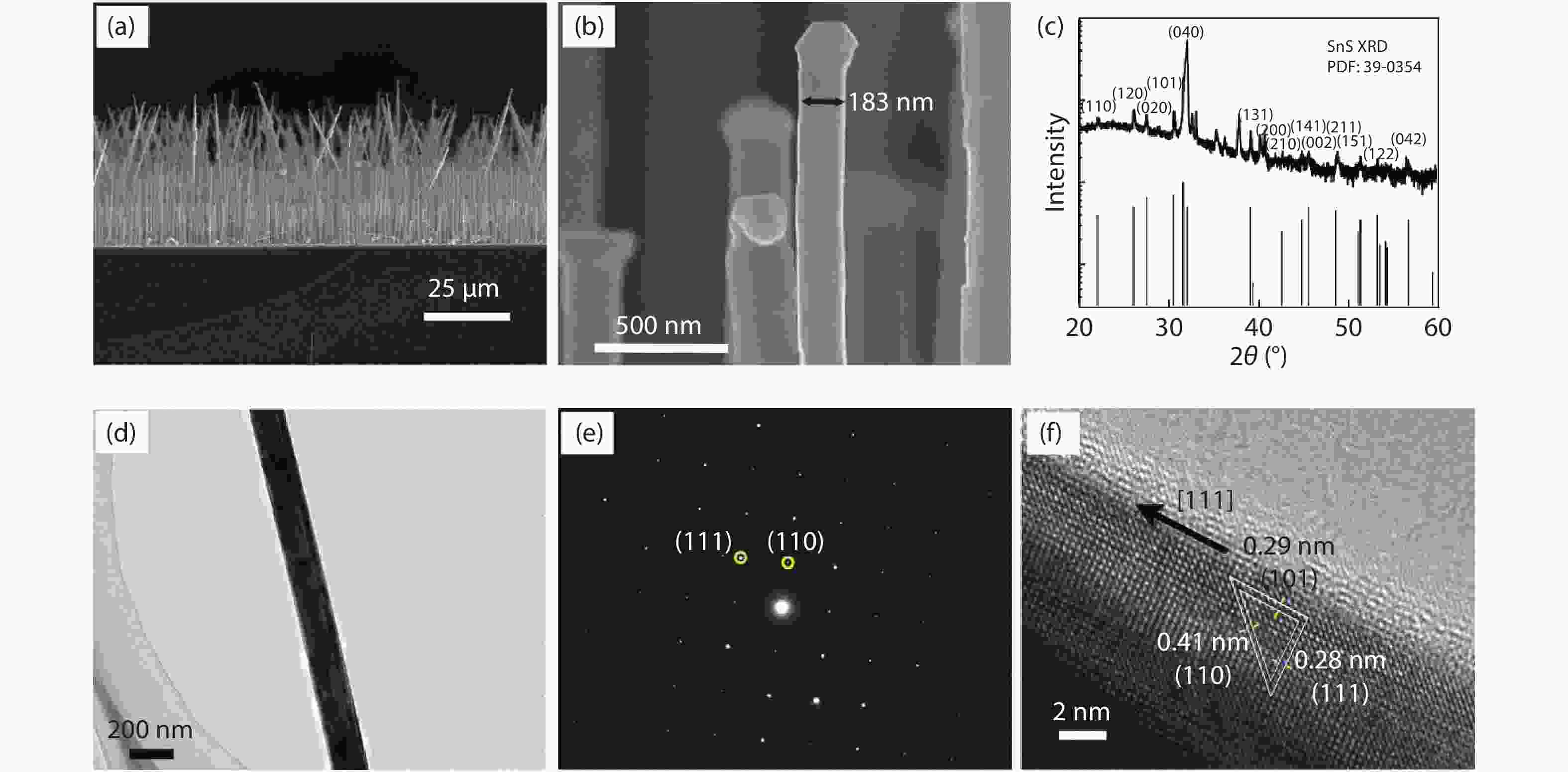
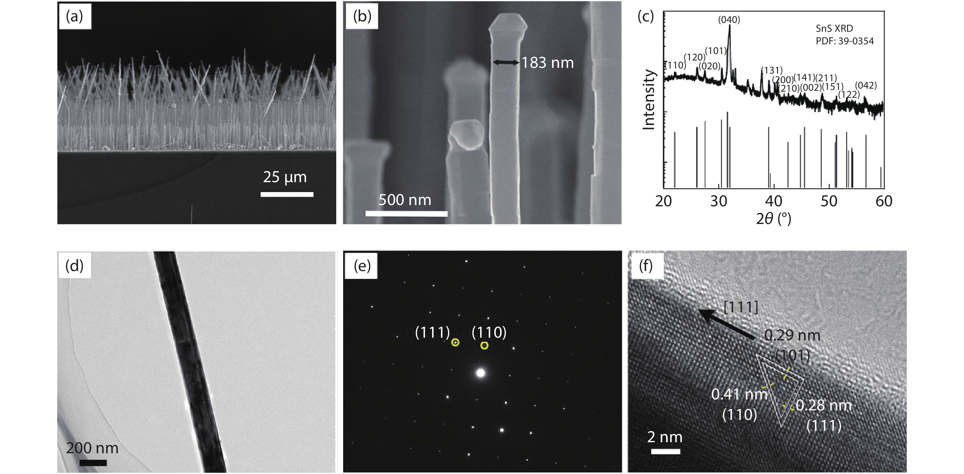
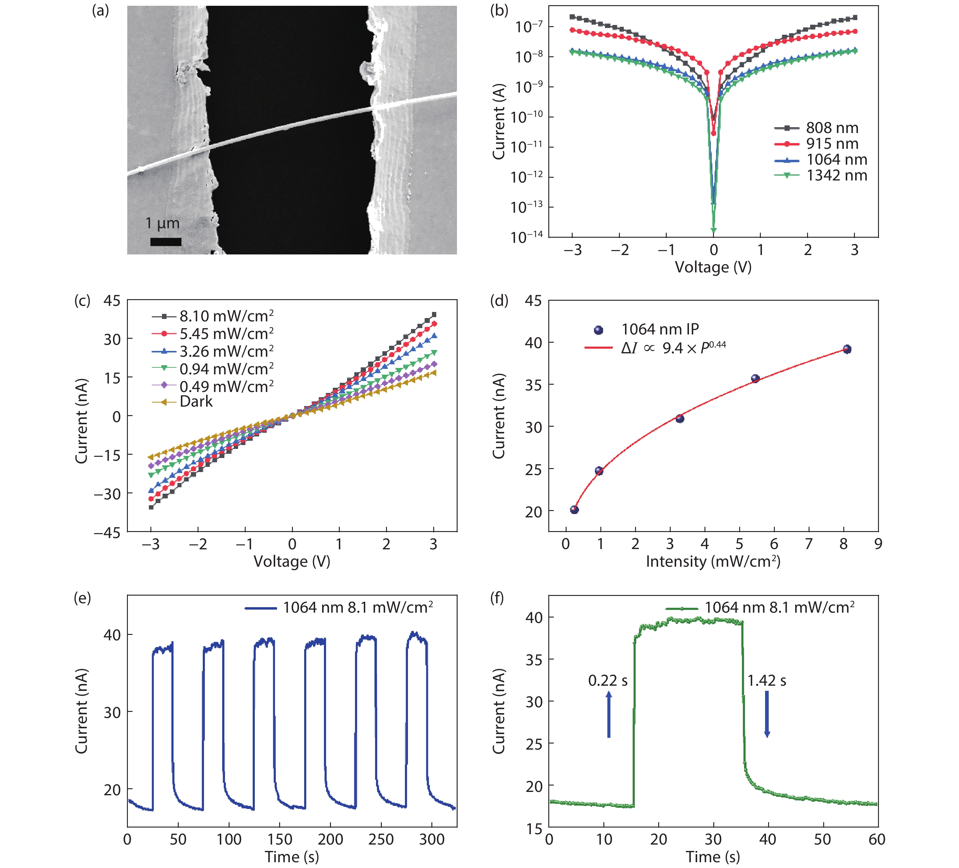
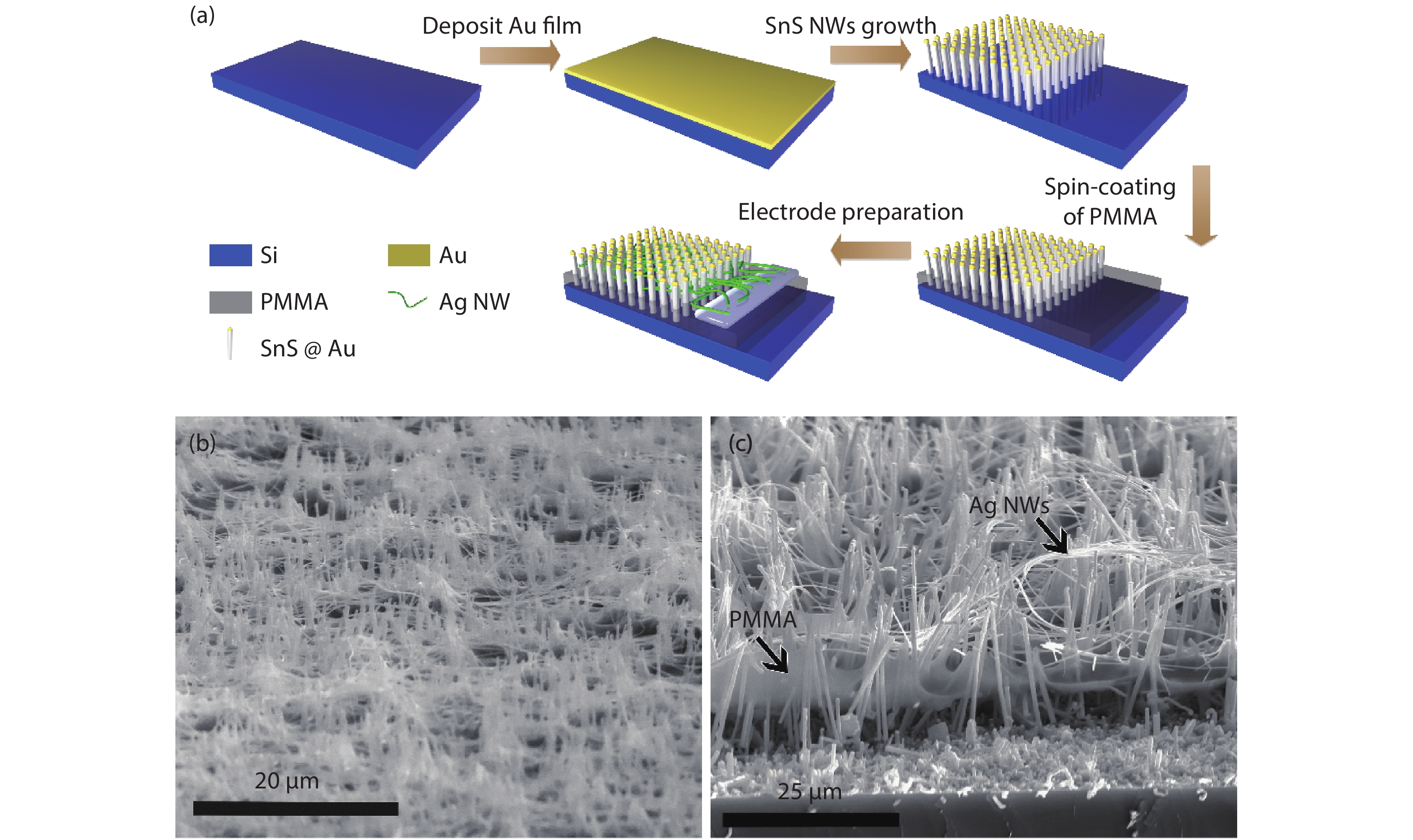
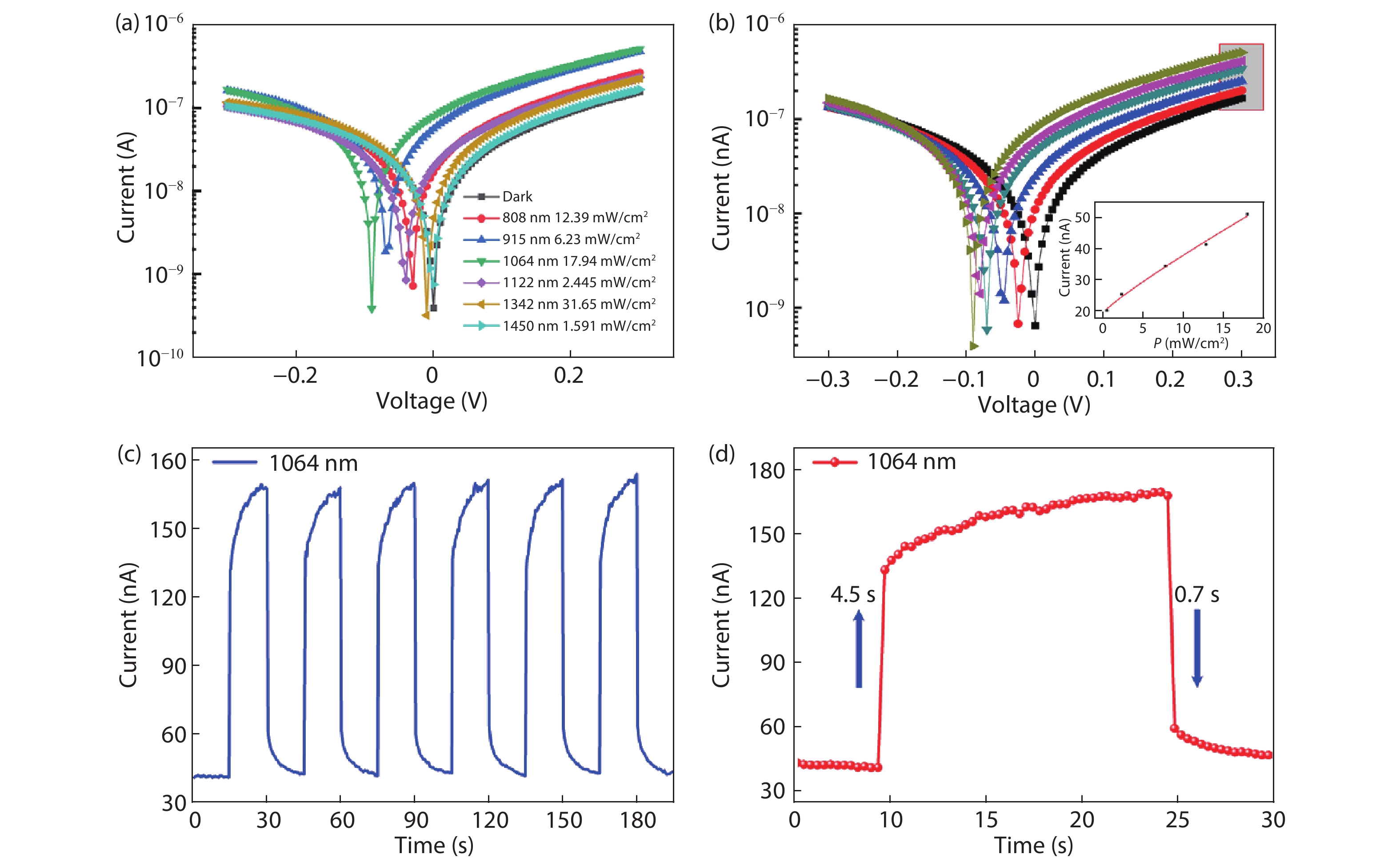
Aligned SnS nanowires arrays were grown via a simple chemical vapor deposition method. As-synthesized SnS nanowires are single crystals grown along the [111] direction. The single SnS nanowire based device showed excellent response to near infrared lights with good responsivity of 267.9 A/W, high external quantum efficiency of 3.12 × 10⁴ % and fast response time. Photodetectors were built on the aligned SnS nanowire arrays, exhibiting a light on/off ratio of 3.6, and the response and decay time of 4.5 and 0.7 s, respectively, to 1064 nm light illumination.