Issue Browser
Volume 46, Issue 12,
Dec 2025
Column
Advancing highly efficient and mechanically resilient flexible perovskite-silicon tandem solar cells
J. Semicond.
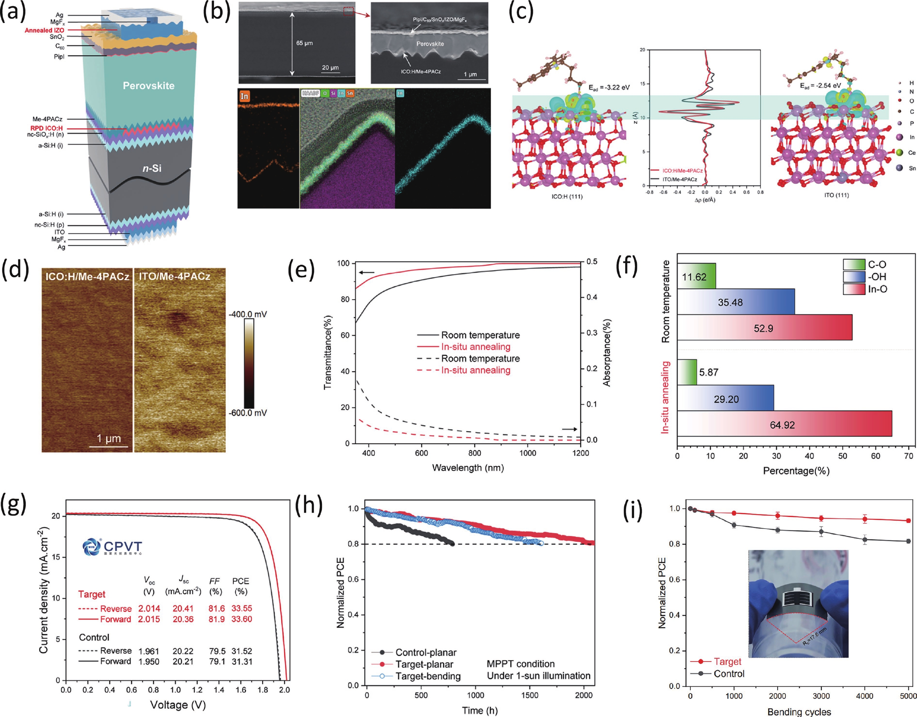
2025, 46(12): 120401 doi: 10.1088/1674-4926/25110013
J. Semicond.
2025, 46(12): 121801 doi: 10.1088/1674-4926/25040012

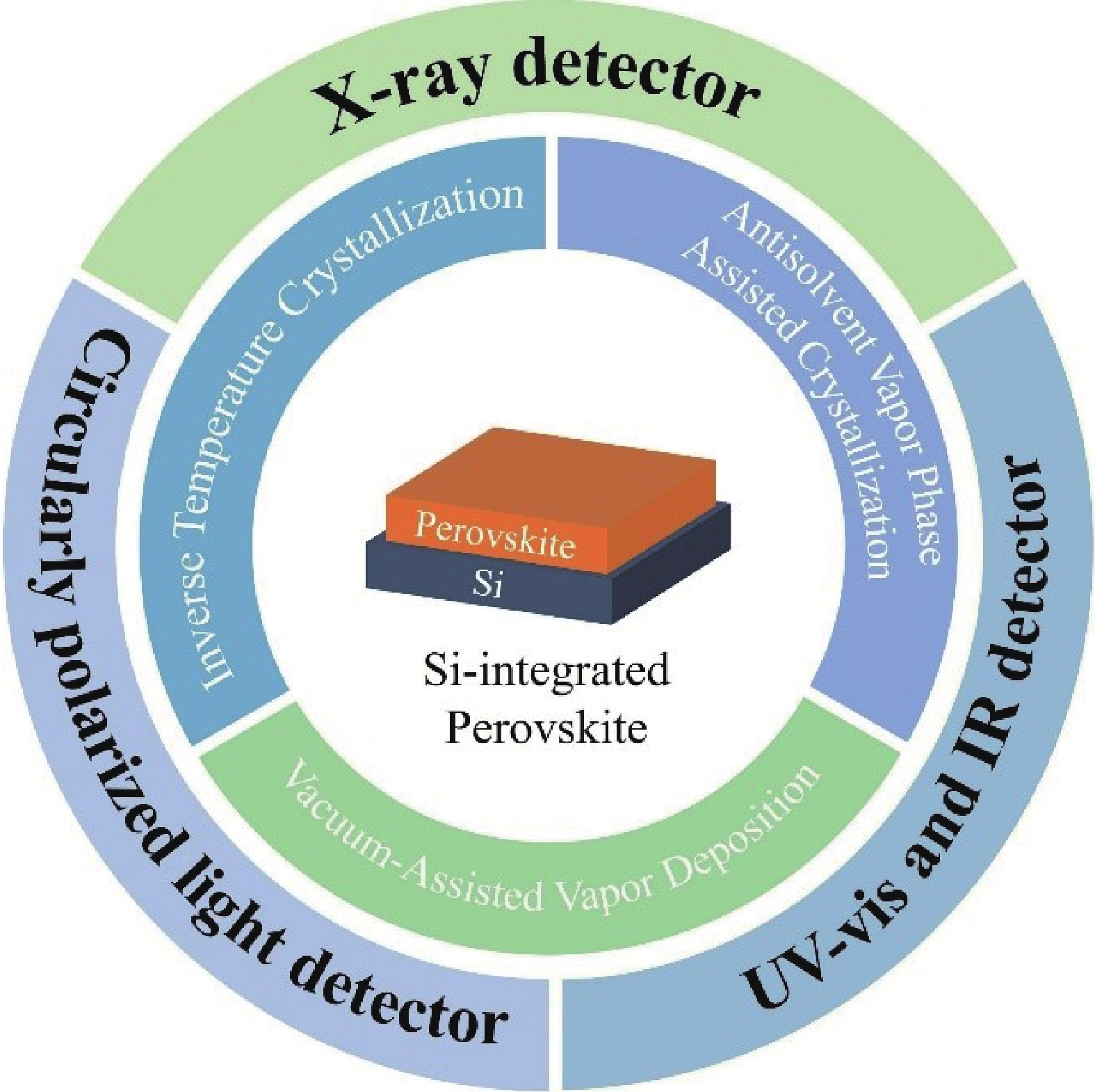
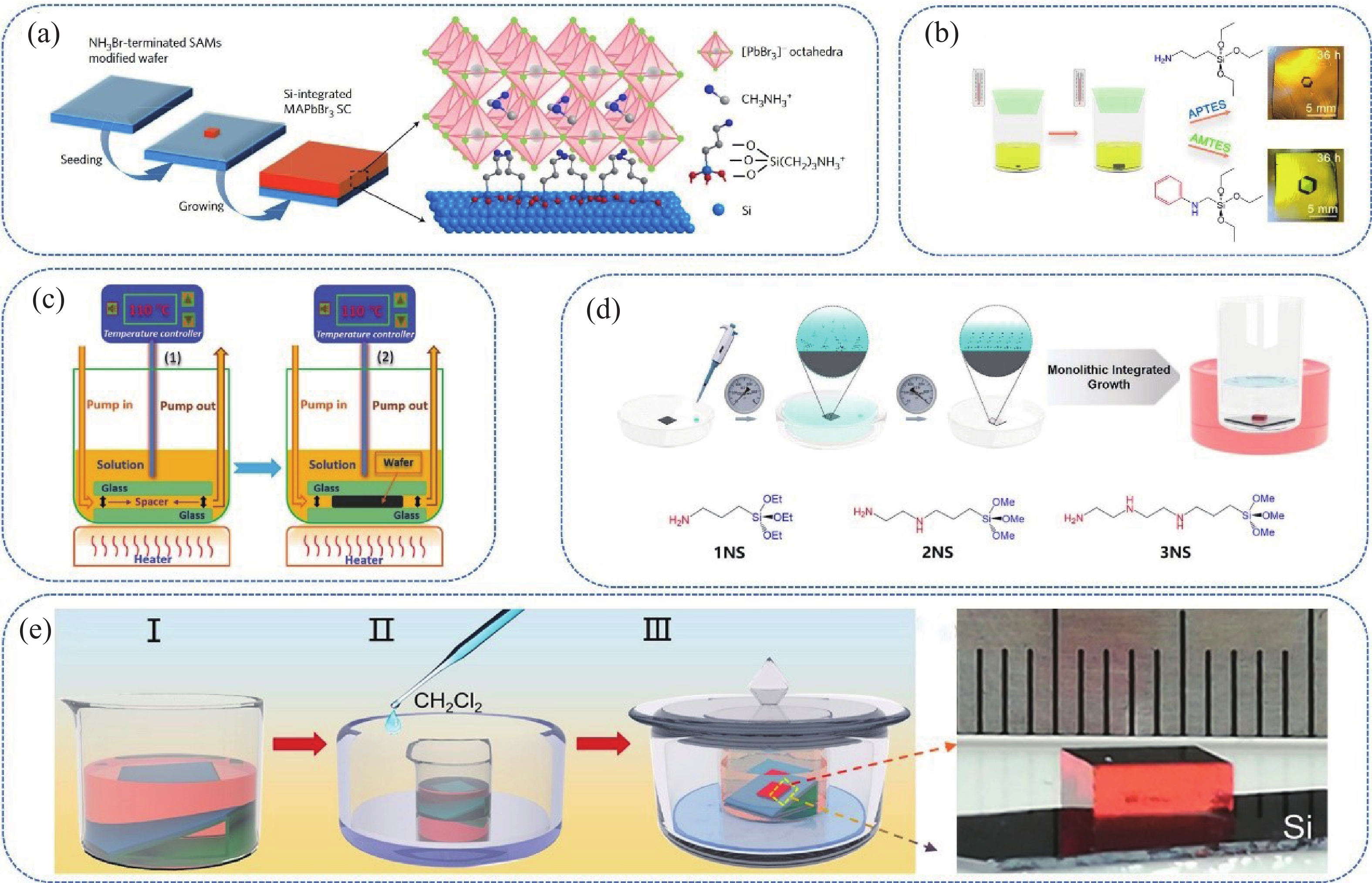
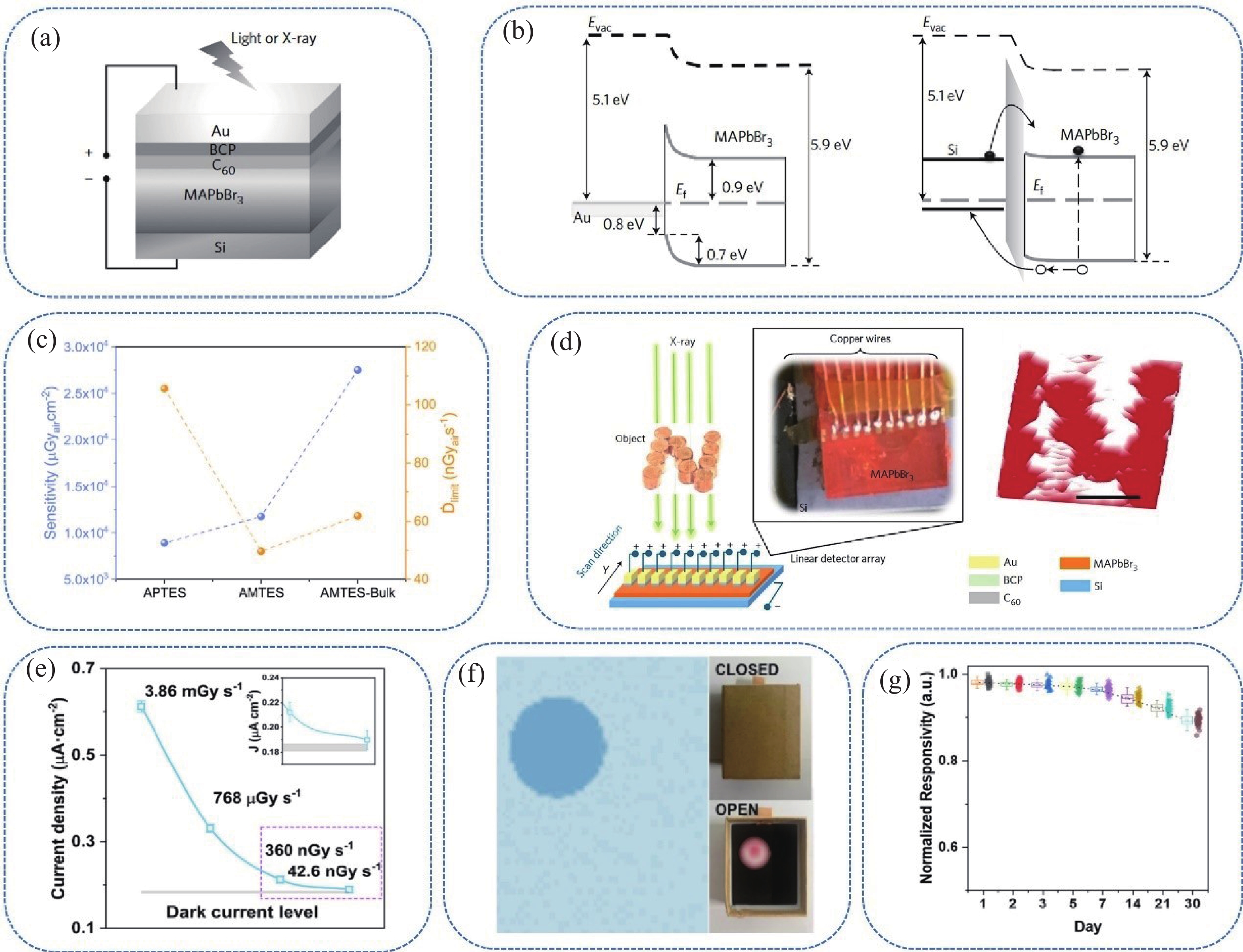
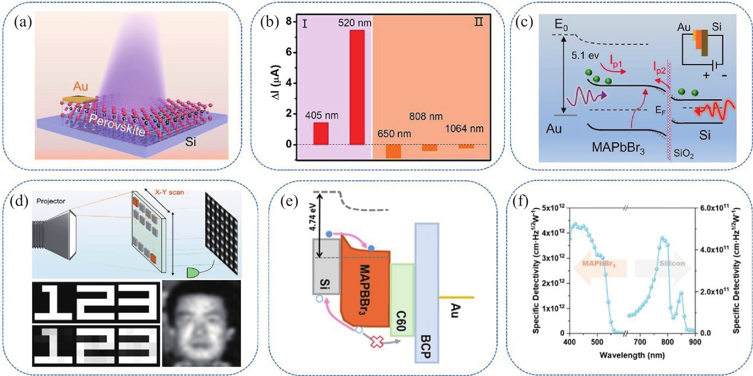
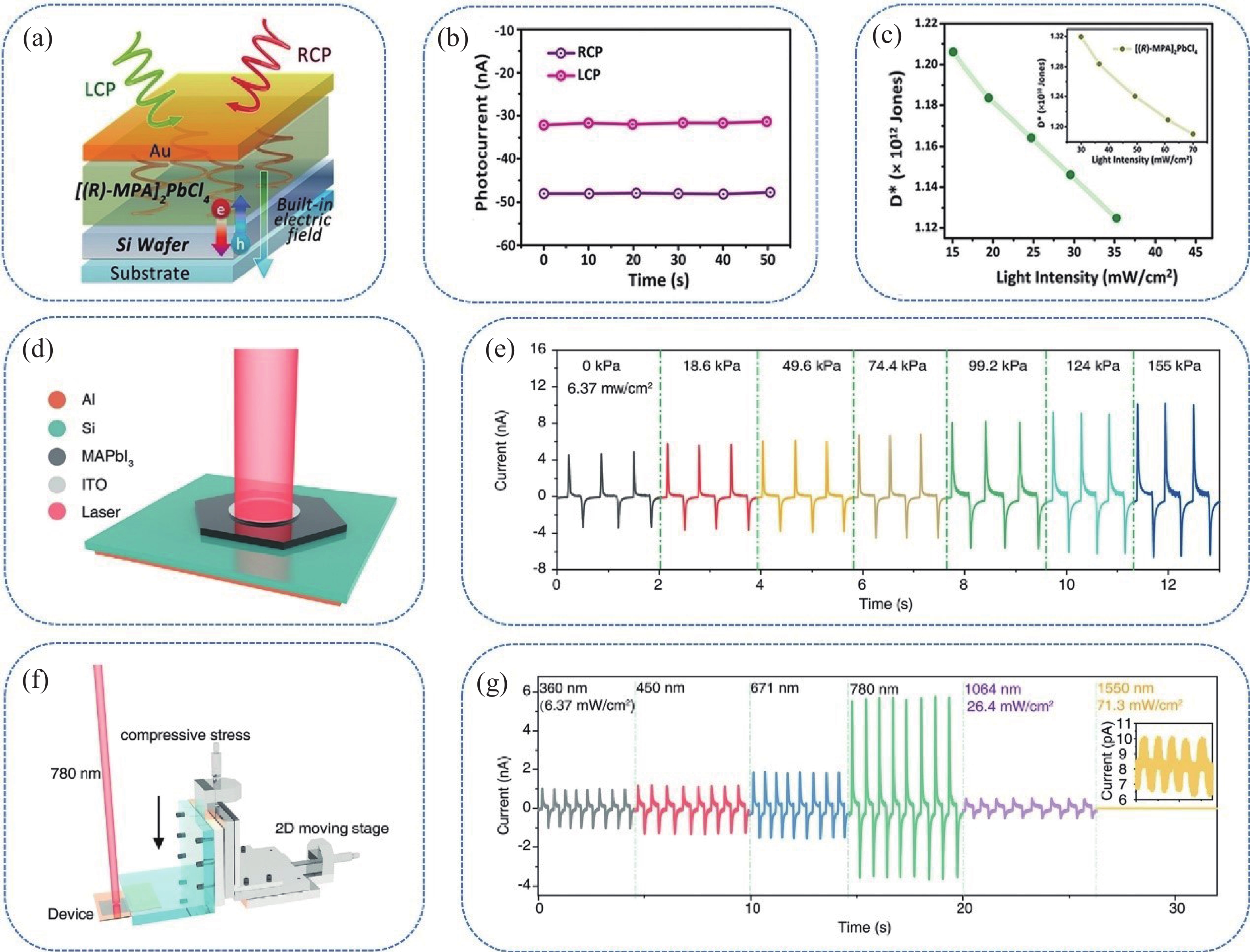
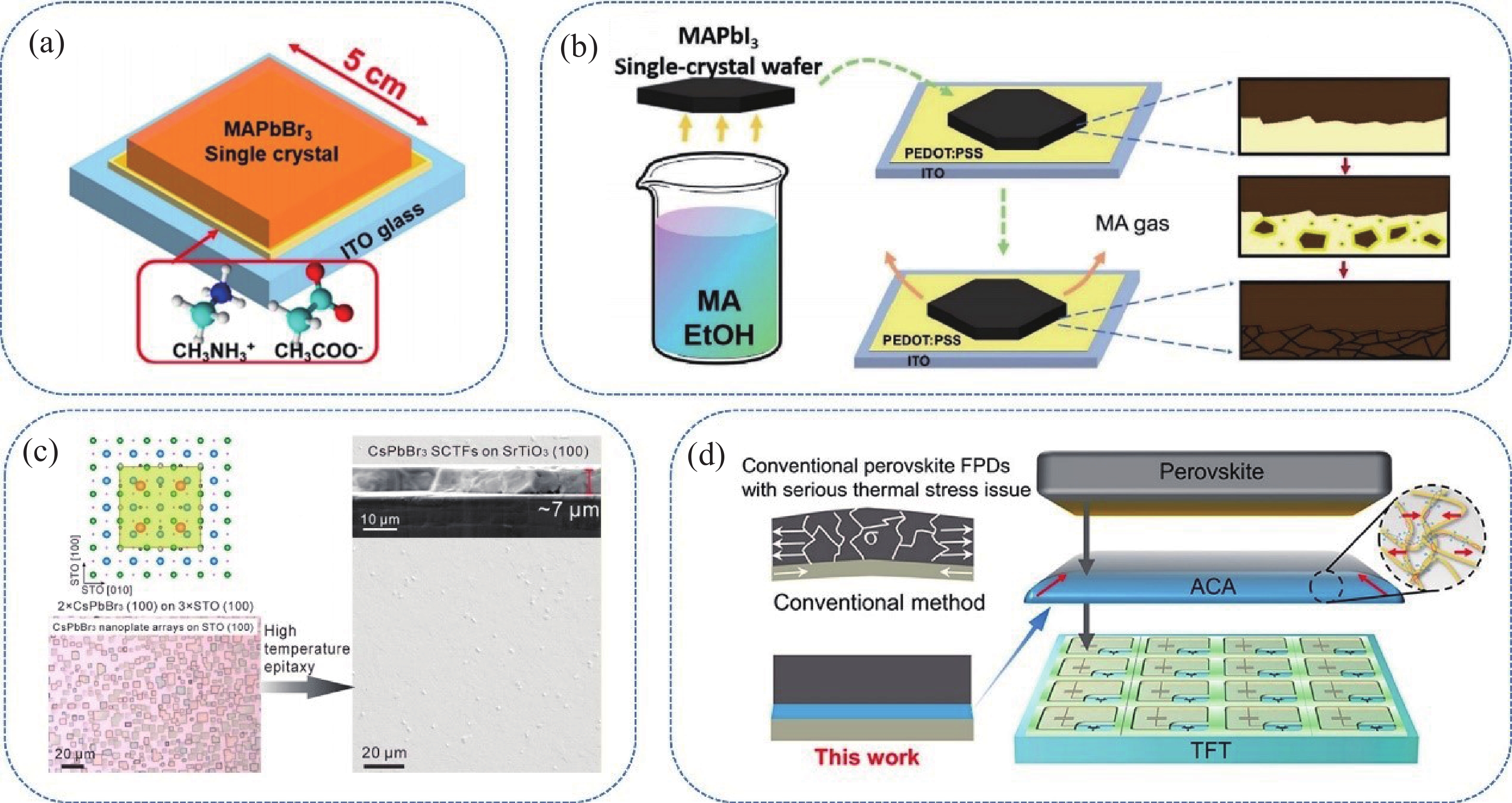
Metal halide perovskites (MHPs) have become promising optoelectronic materials due to their long carrier lifetimes and high mobility. However, the presence of defects and ion migration in MHPs results in high and unstable dark currents, which compromise the stability and detection performance of MHP-based optoelectronic devices. Interfacial engineering has proven to be an effective strategy to reduce defect density in MHPs and suppress ion migration. Given the compatibility of silicon (Si) and MHP processing technologies, coupled with the simplicity and cost-effectiveness of the approach, the integration of MHPs onto Si surfaces has become a prominent area of research. This integration not only enhances device performance but also expands their practical applications. This review provides an overview of the integration technologies for Si and single crystal MHPs, evaluates the advantages and limitations of various integration schemes (including inverse temperature crystallization, vacuum-assisted vapor deposition, and anti-solvent vapor-assisted crystallization), and explores the practical applications of Si/MHP-integrated optoelectronic devices with different structures. These optimized devices exhibit outstanding performance in X-ray detection, multi-wavelength photodetection, and circularly polarized light detection. This review provides a systematic reference for technological innovation and application expansion of Si/MHP-integrated devices.
J. Semicond.
2025, 46(12): 122101 doi: 10.1088/1674-4926/25040013
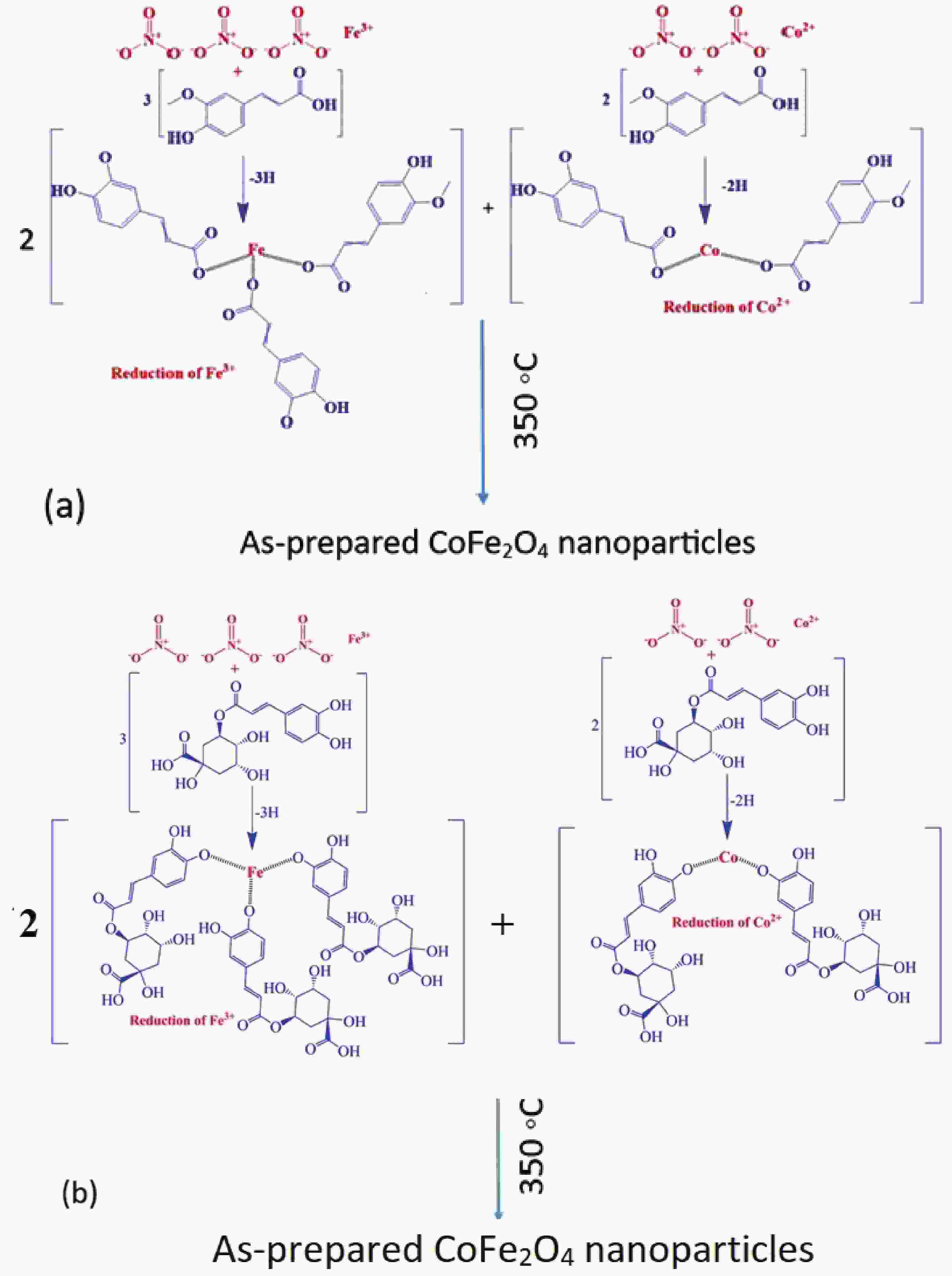
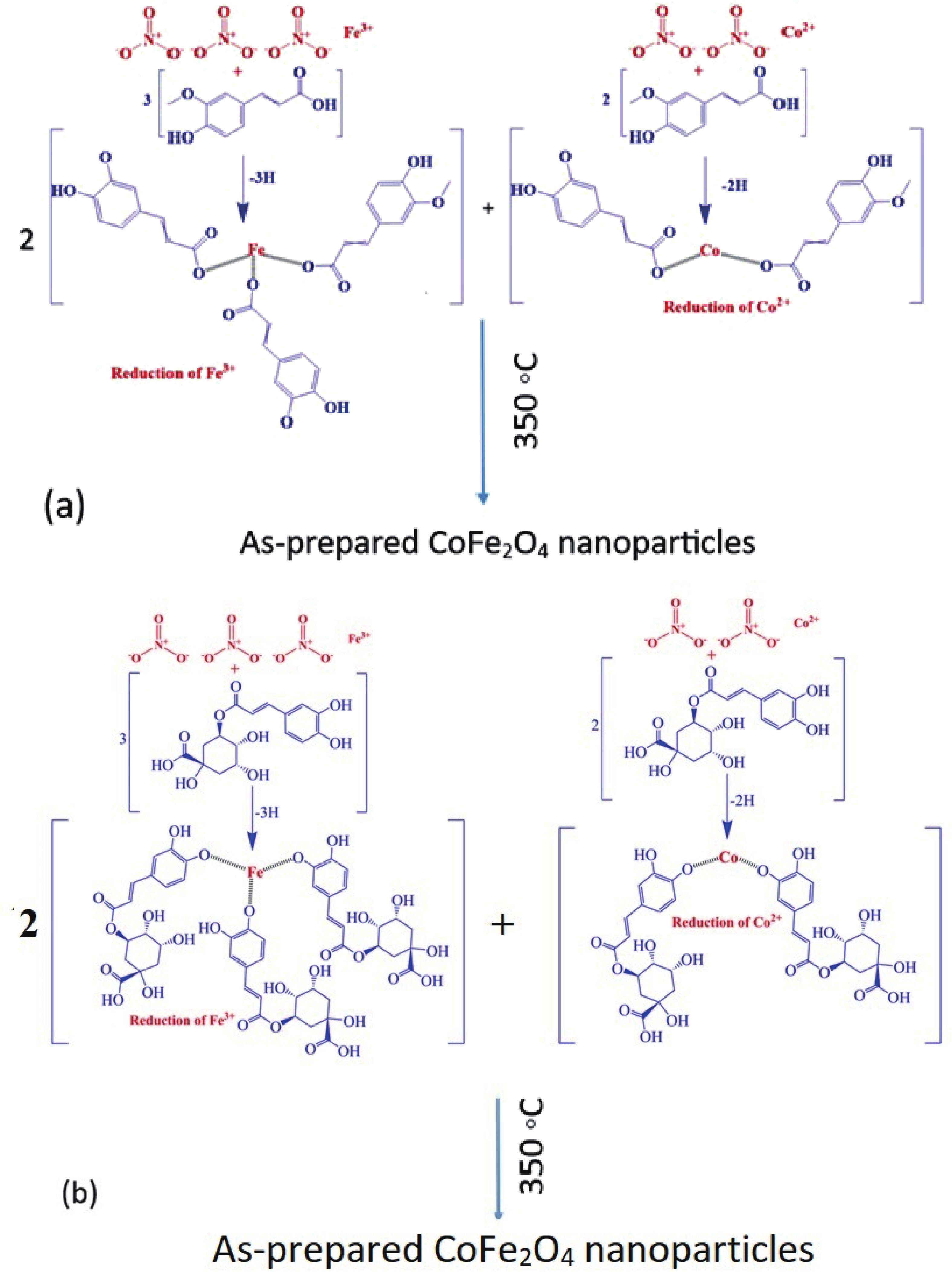
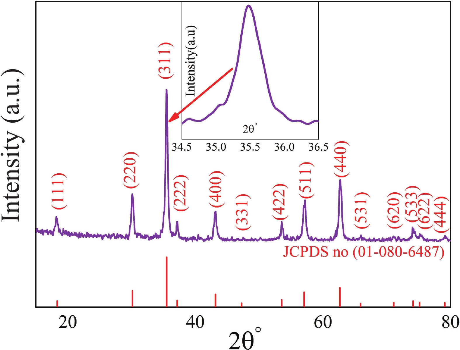
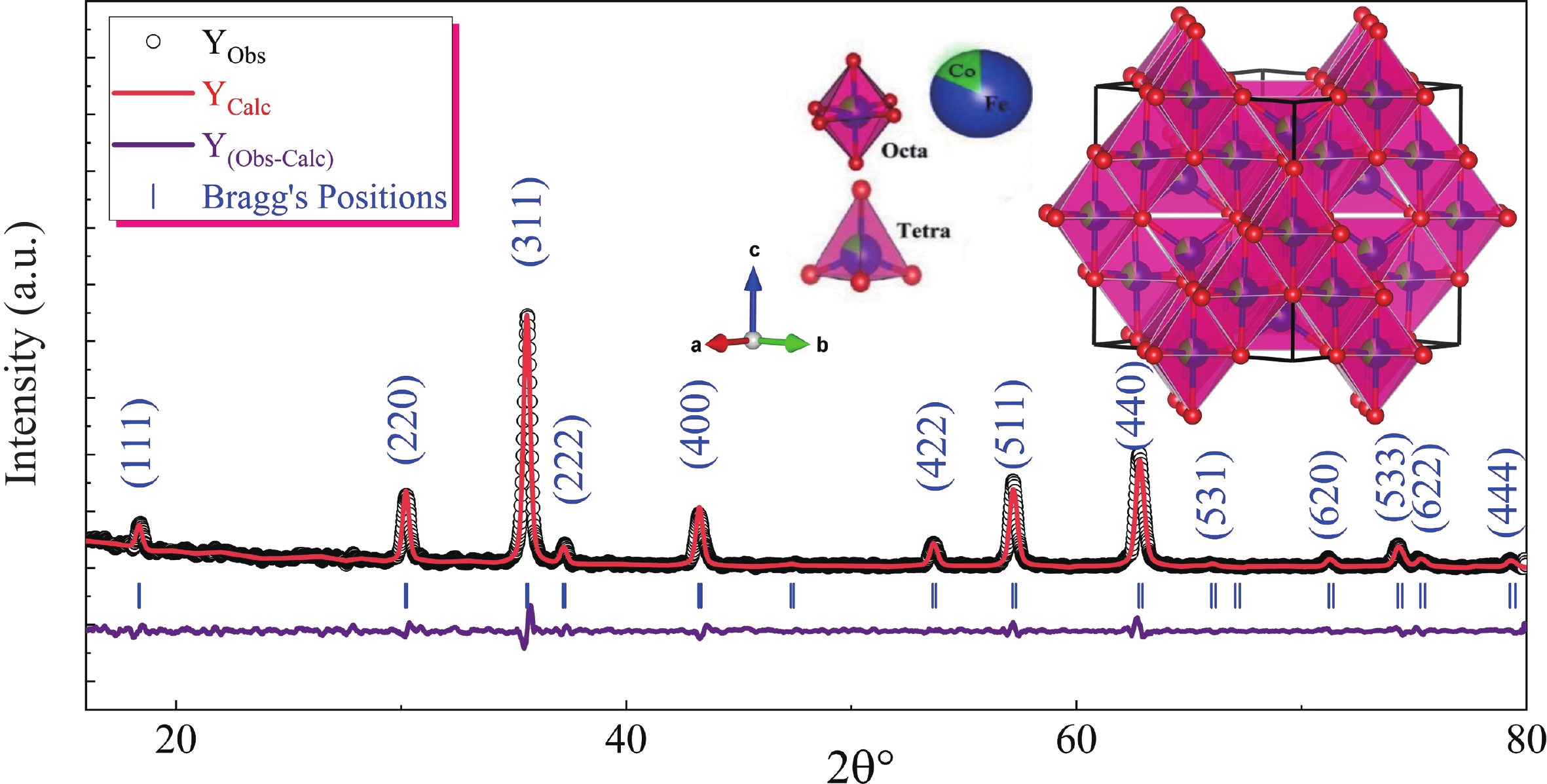
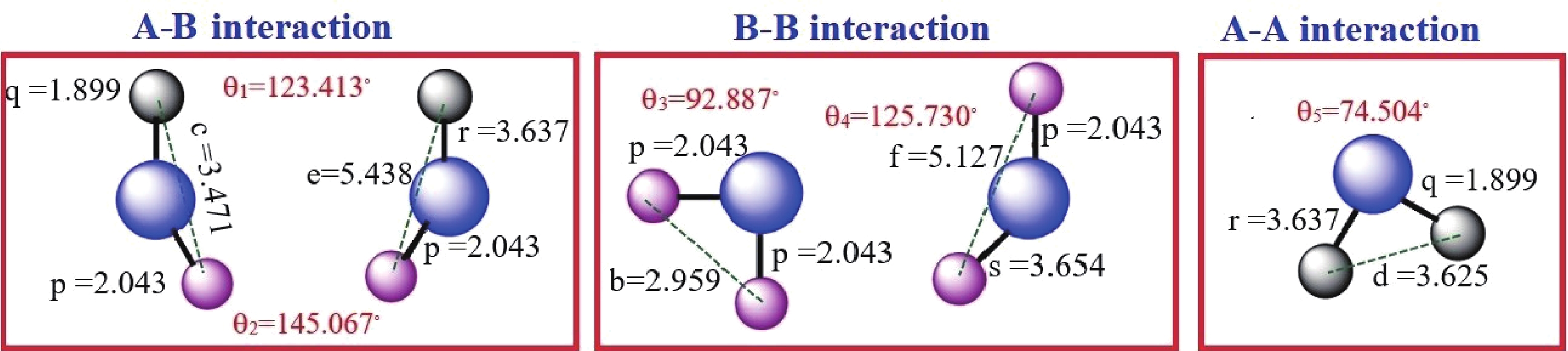
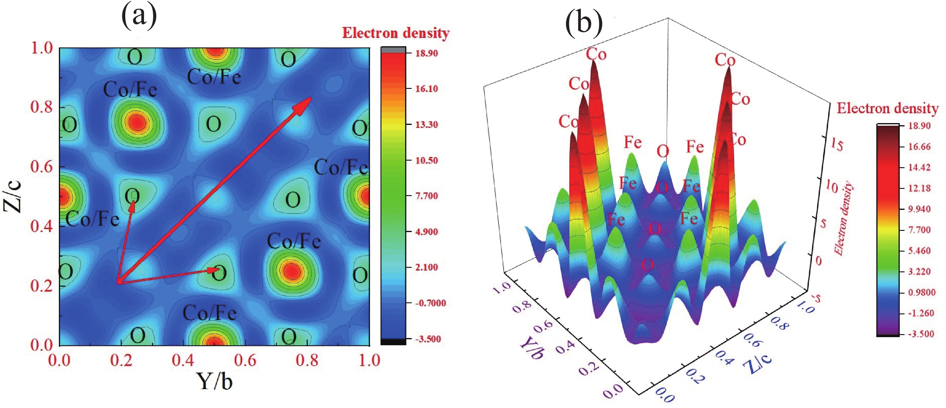
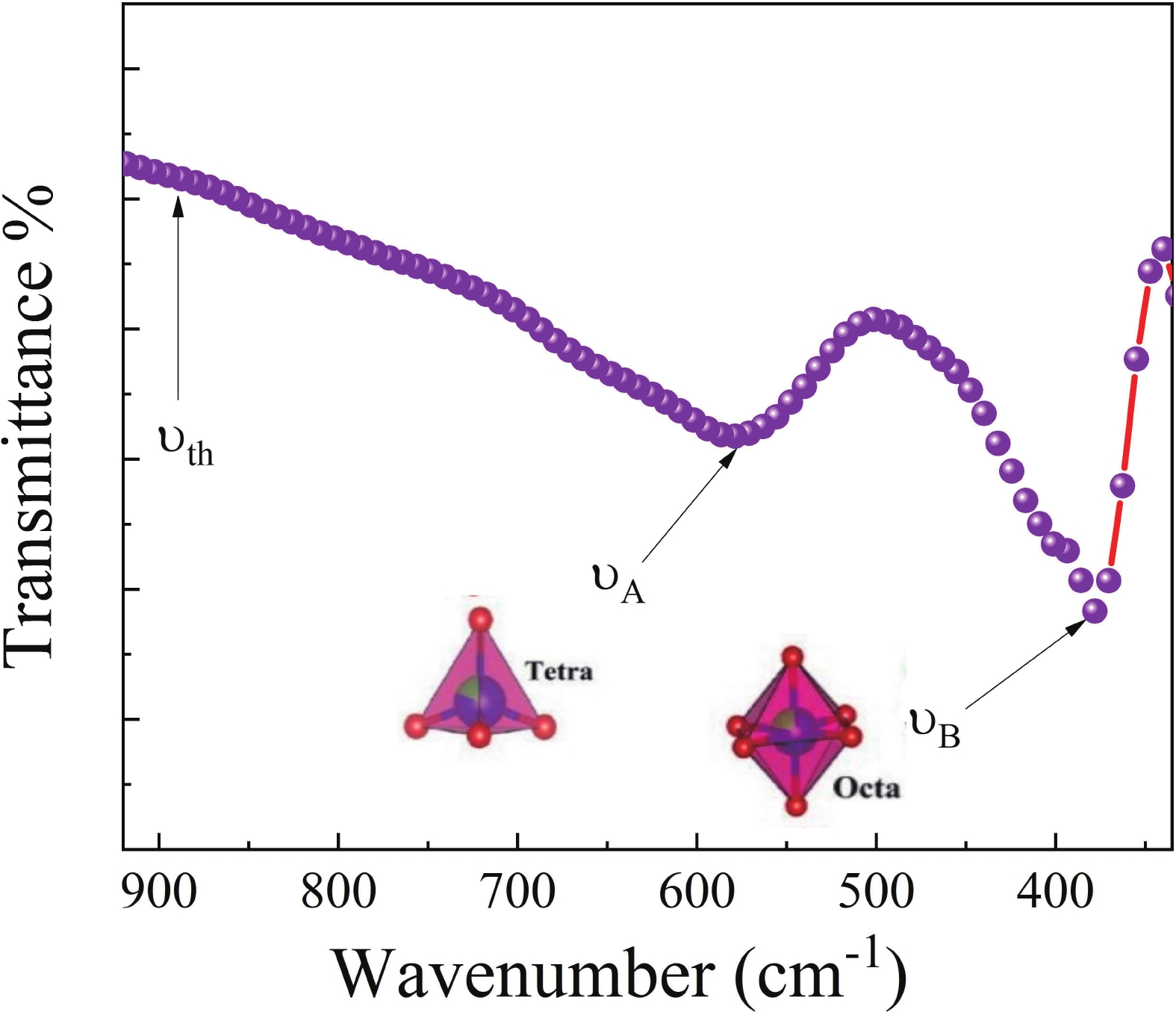
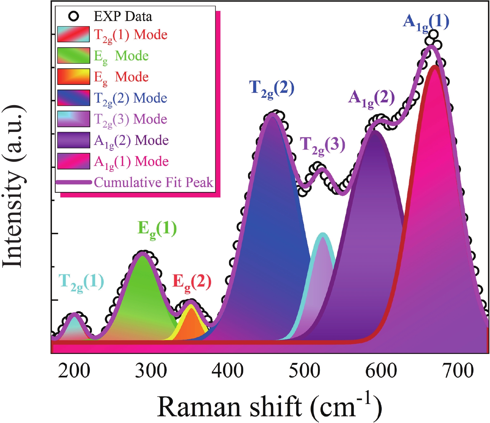
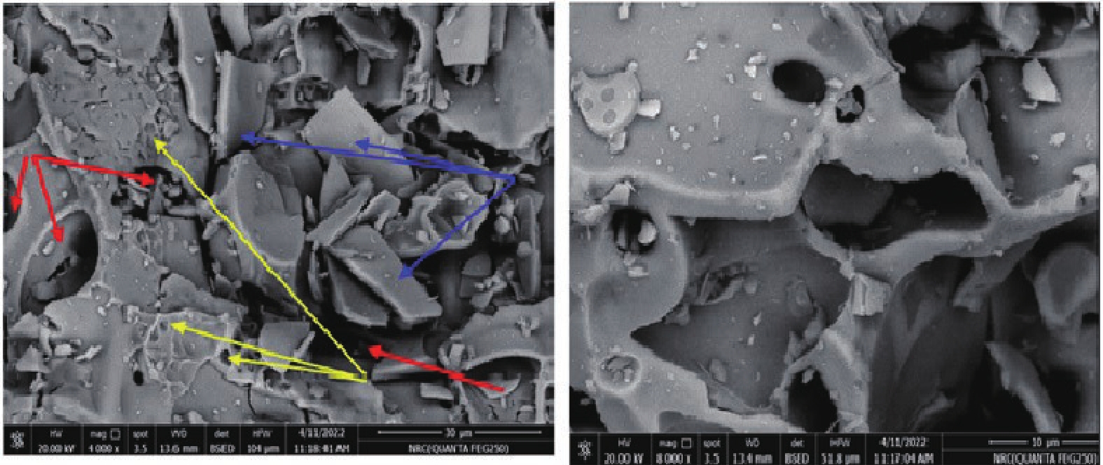
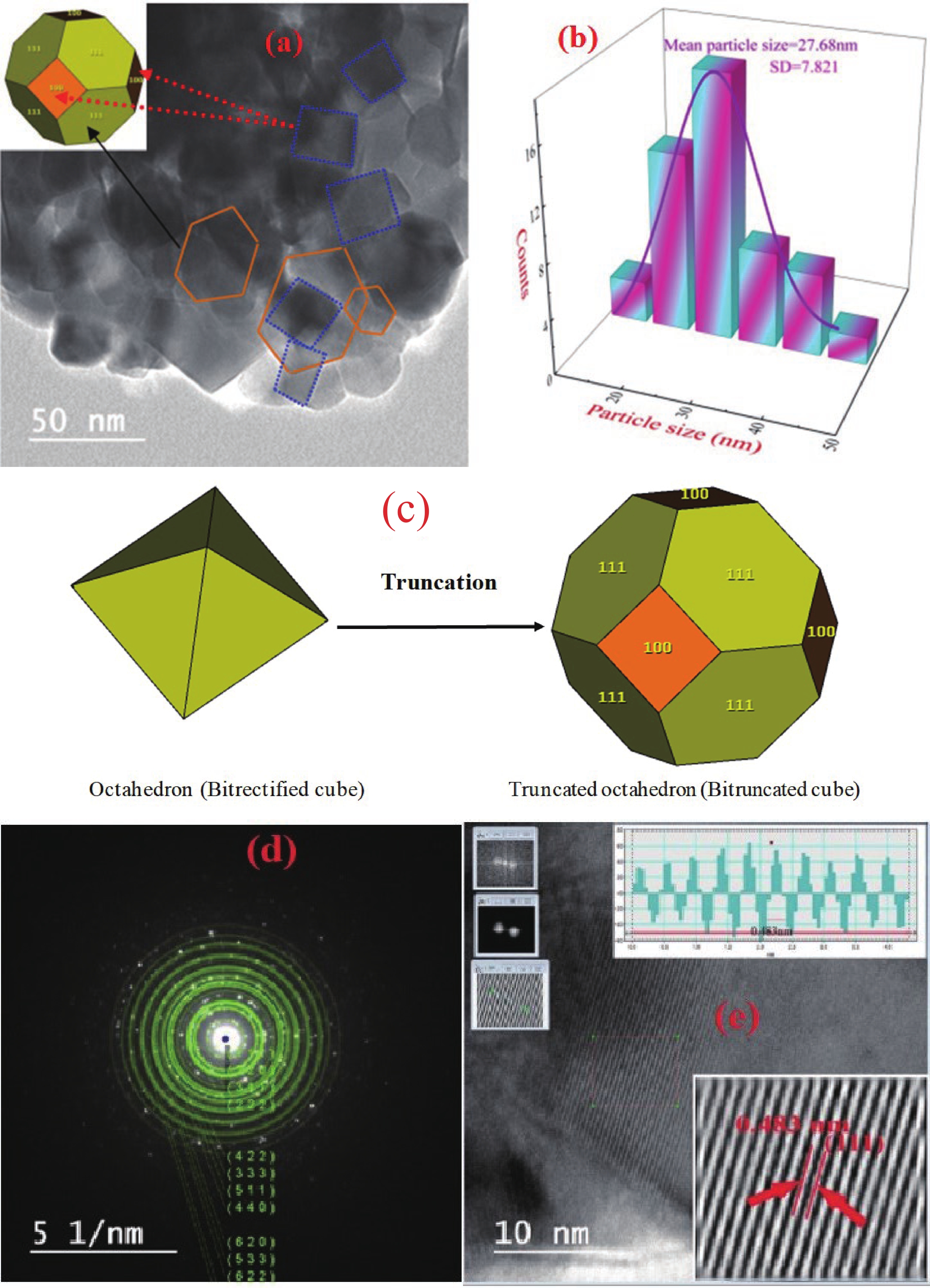
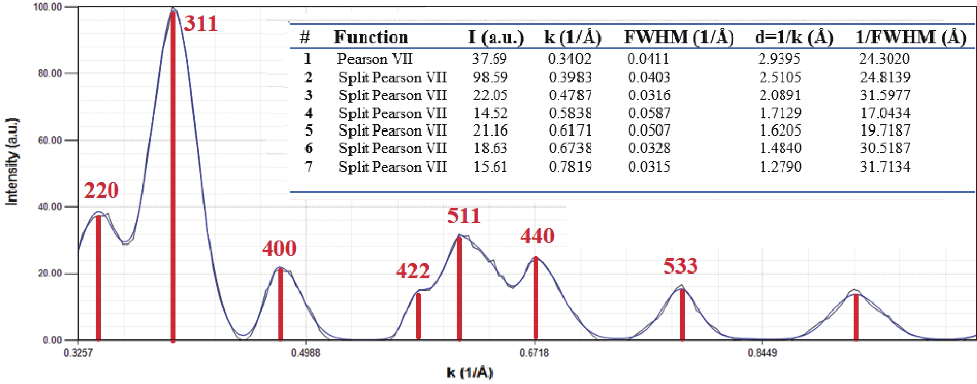
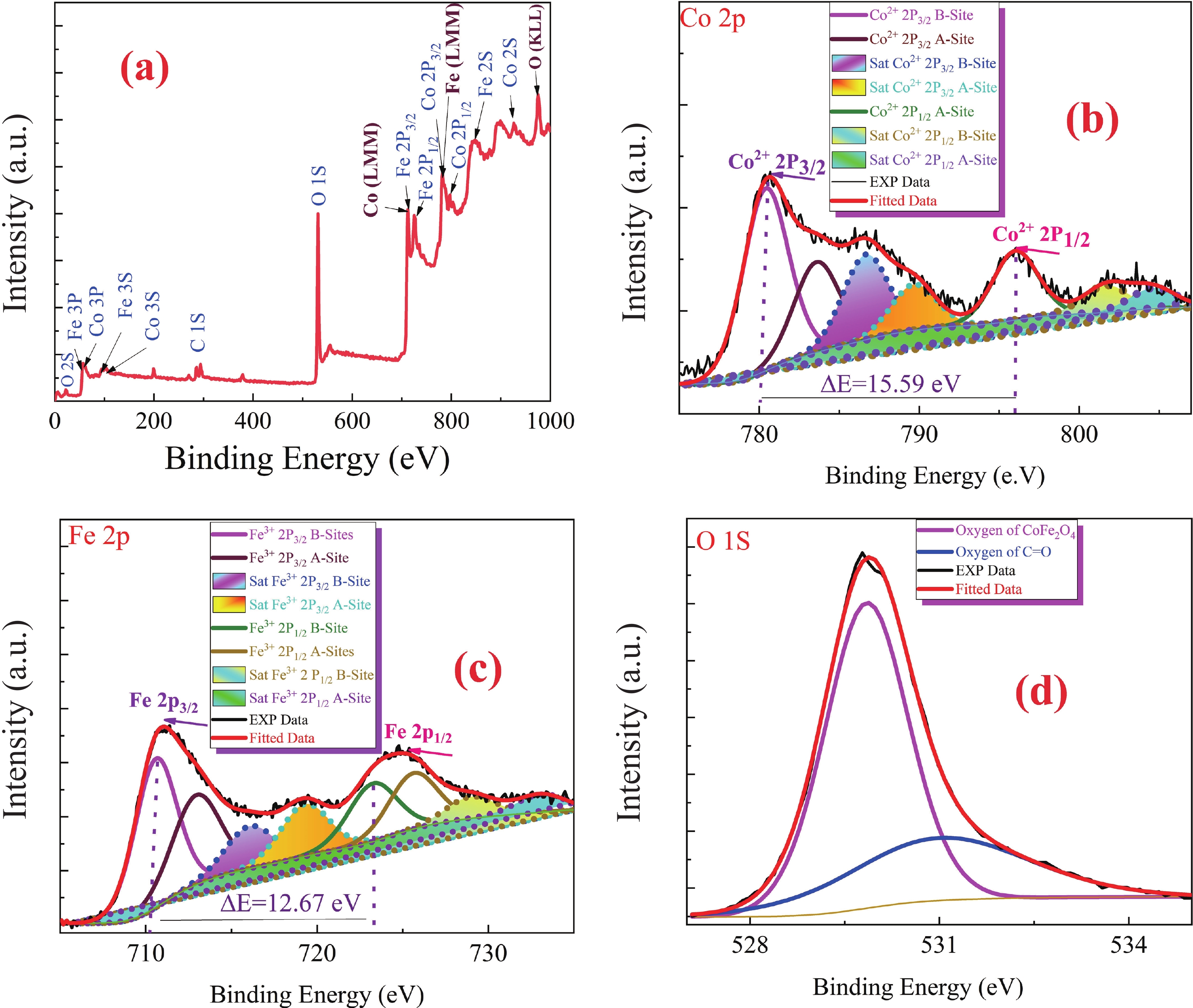
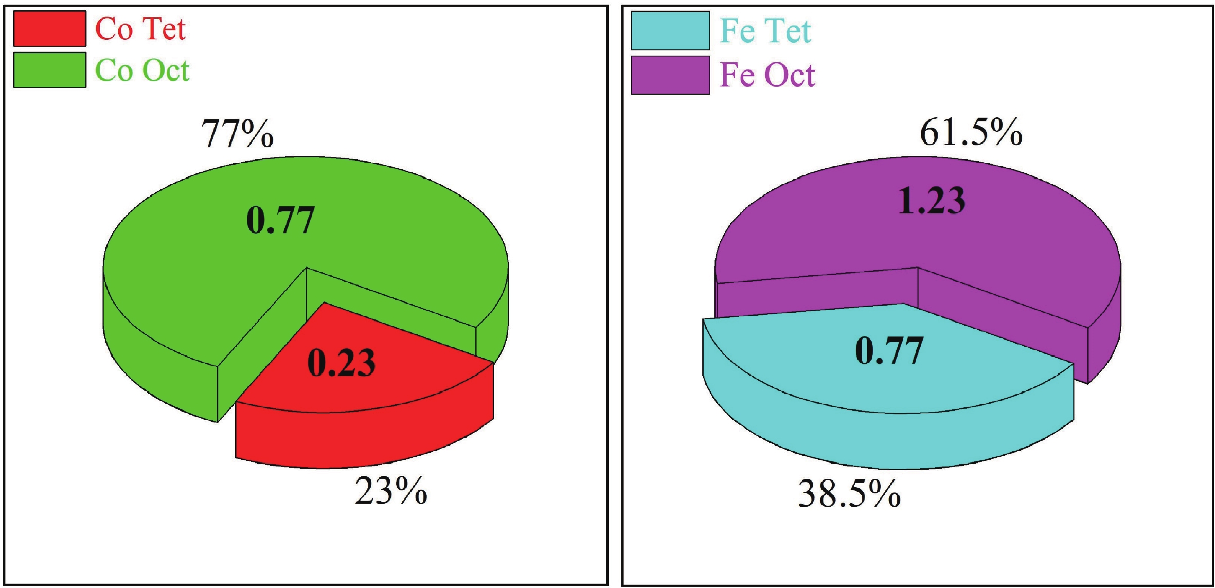
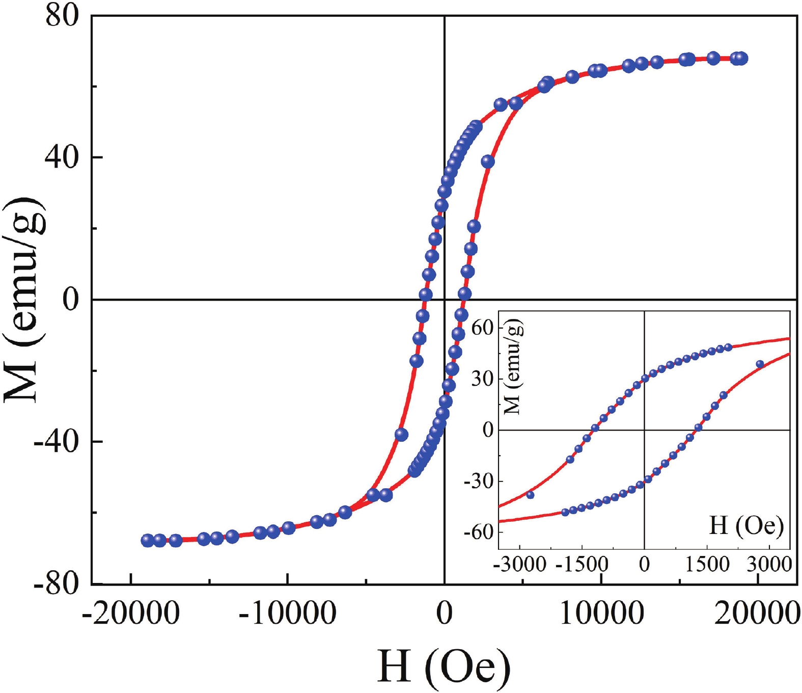
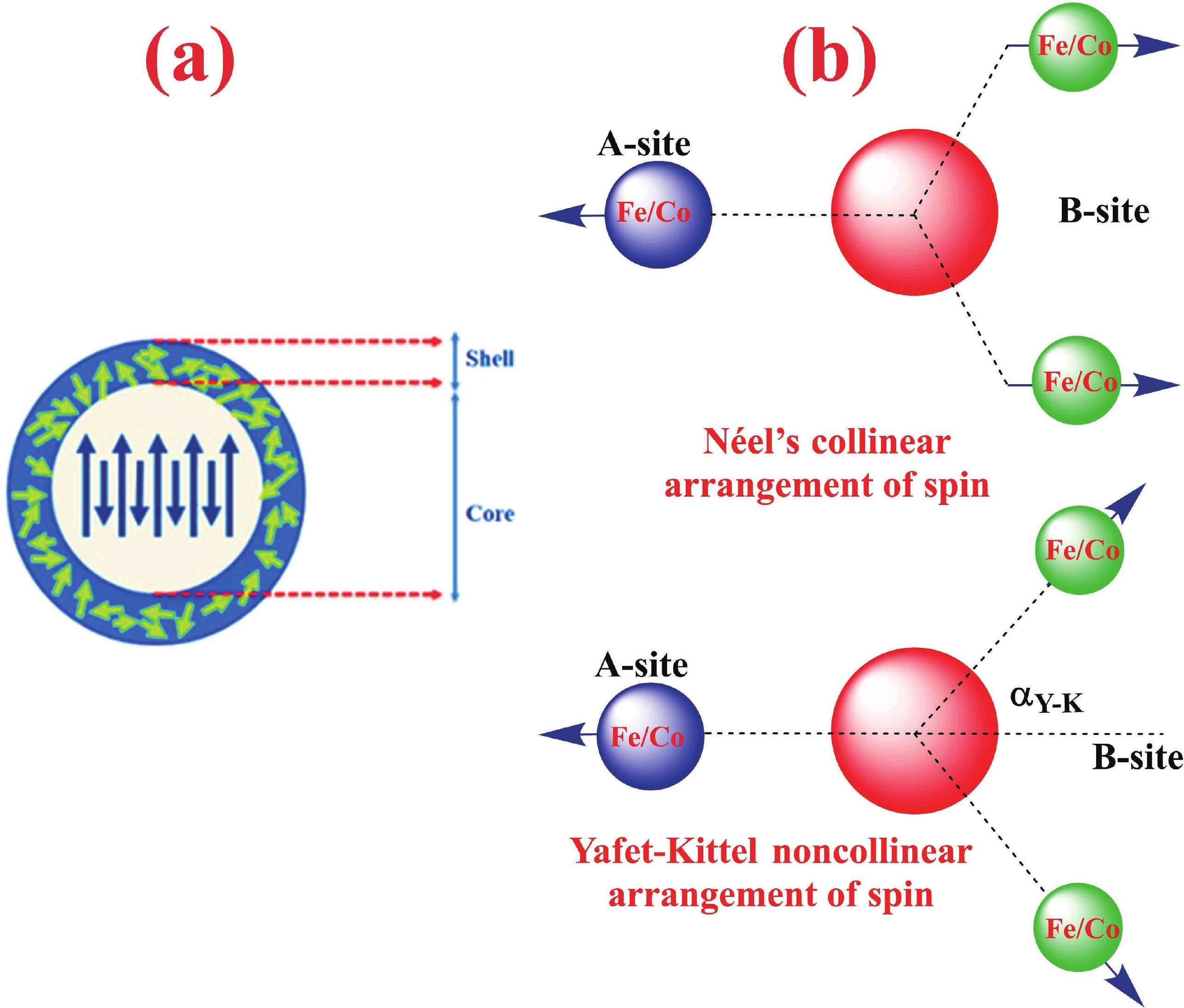
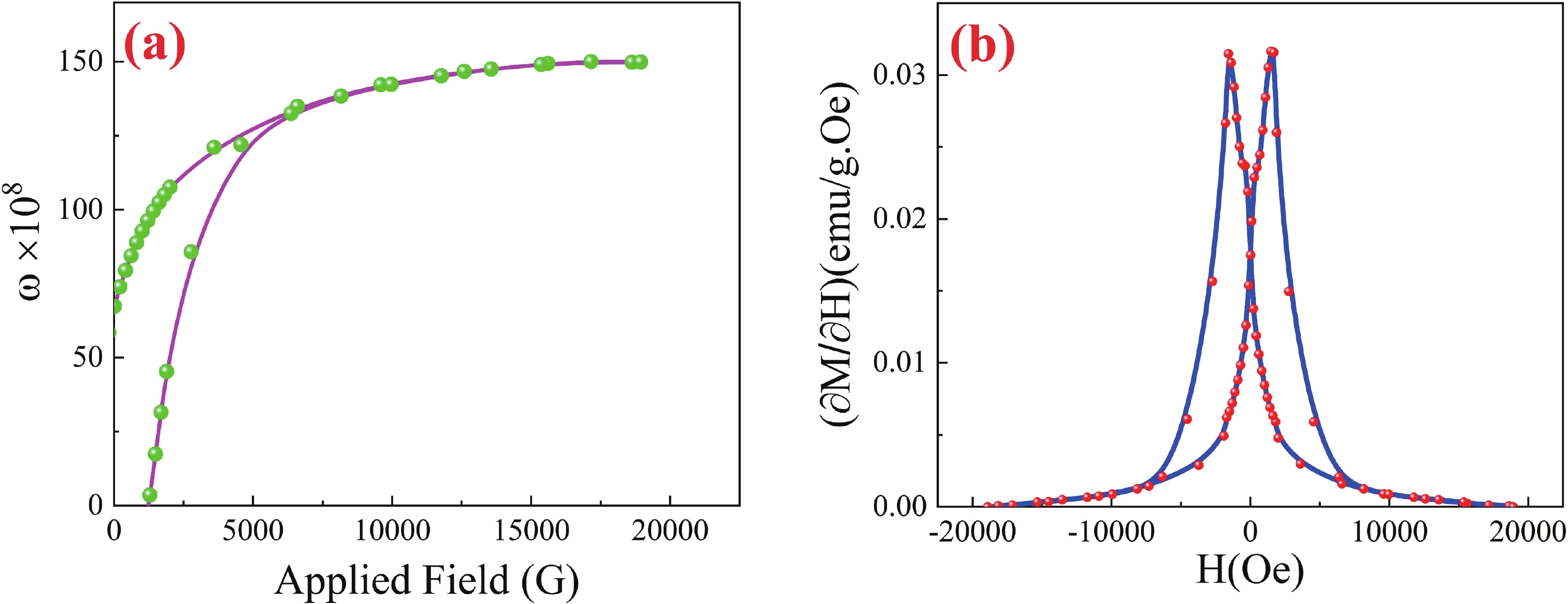
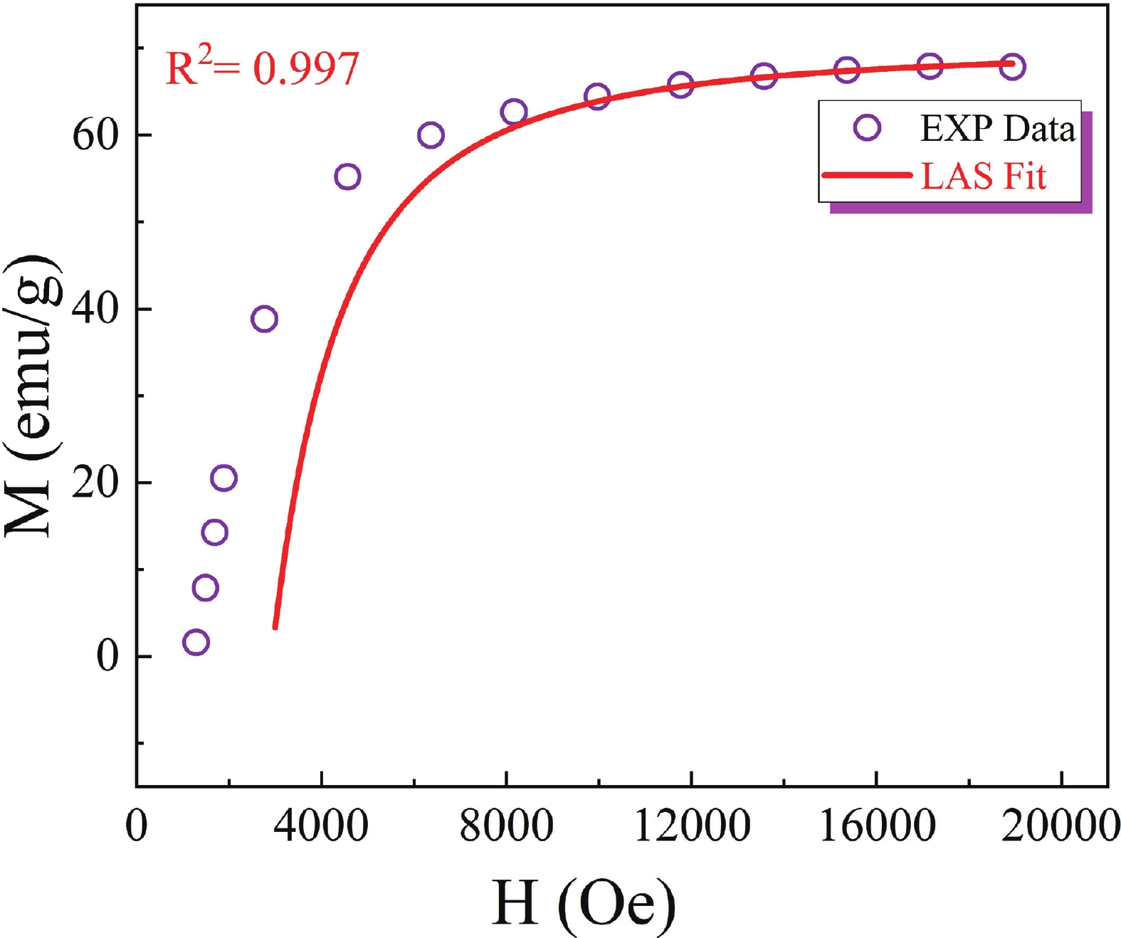
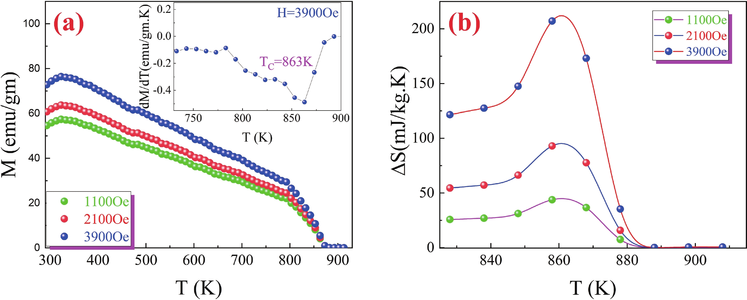
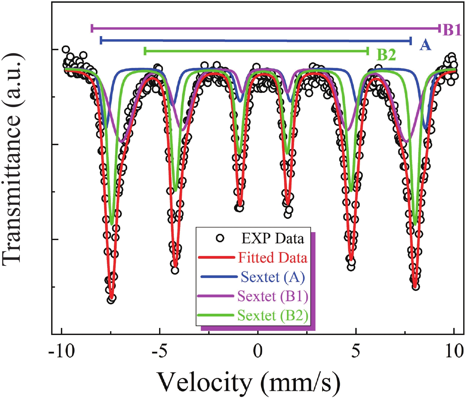
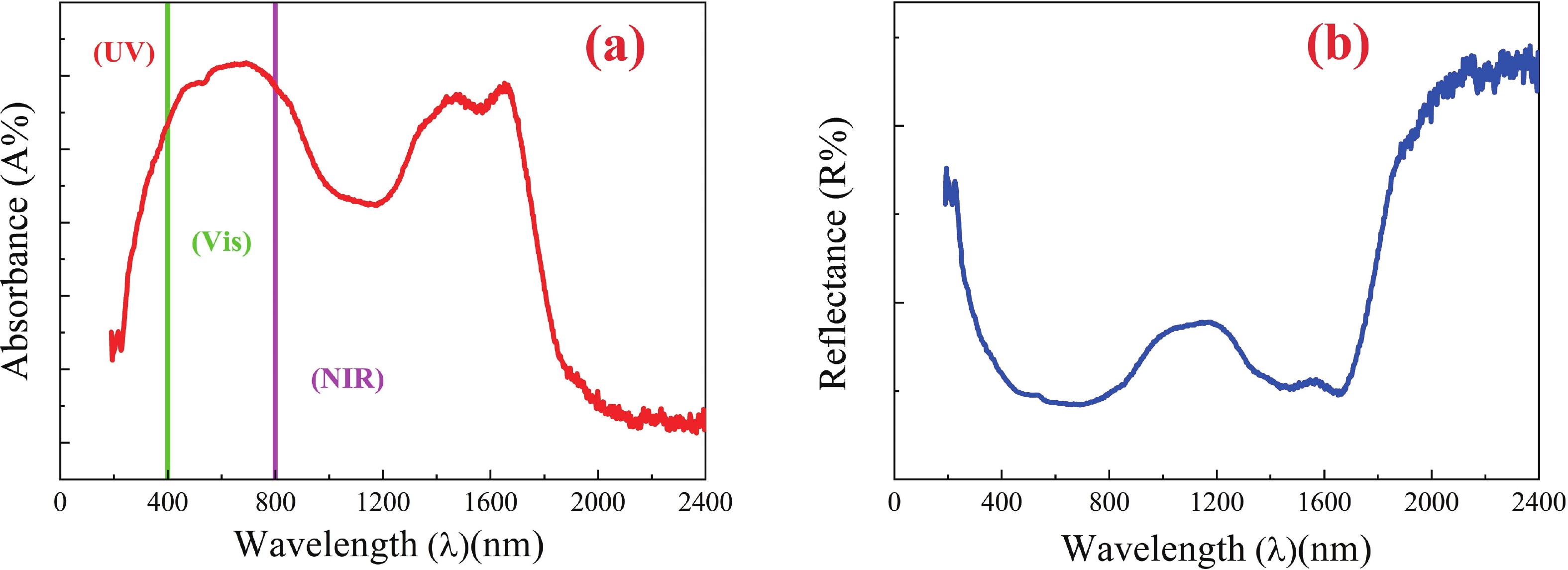
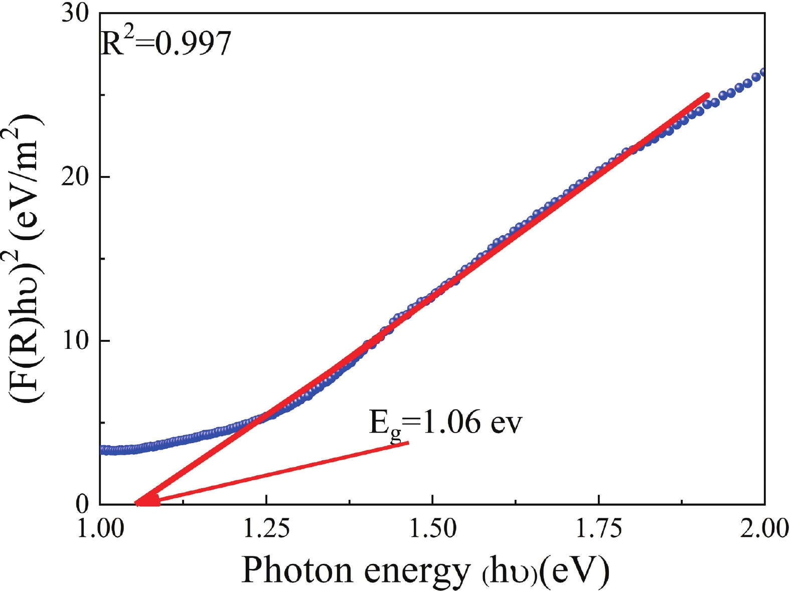
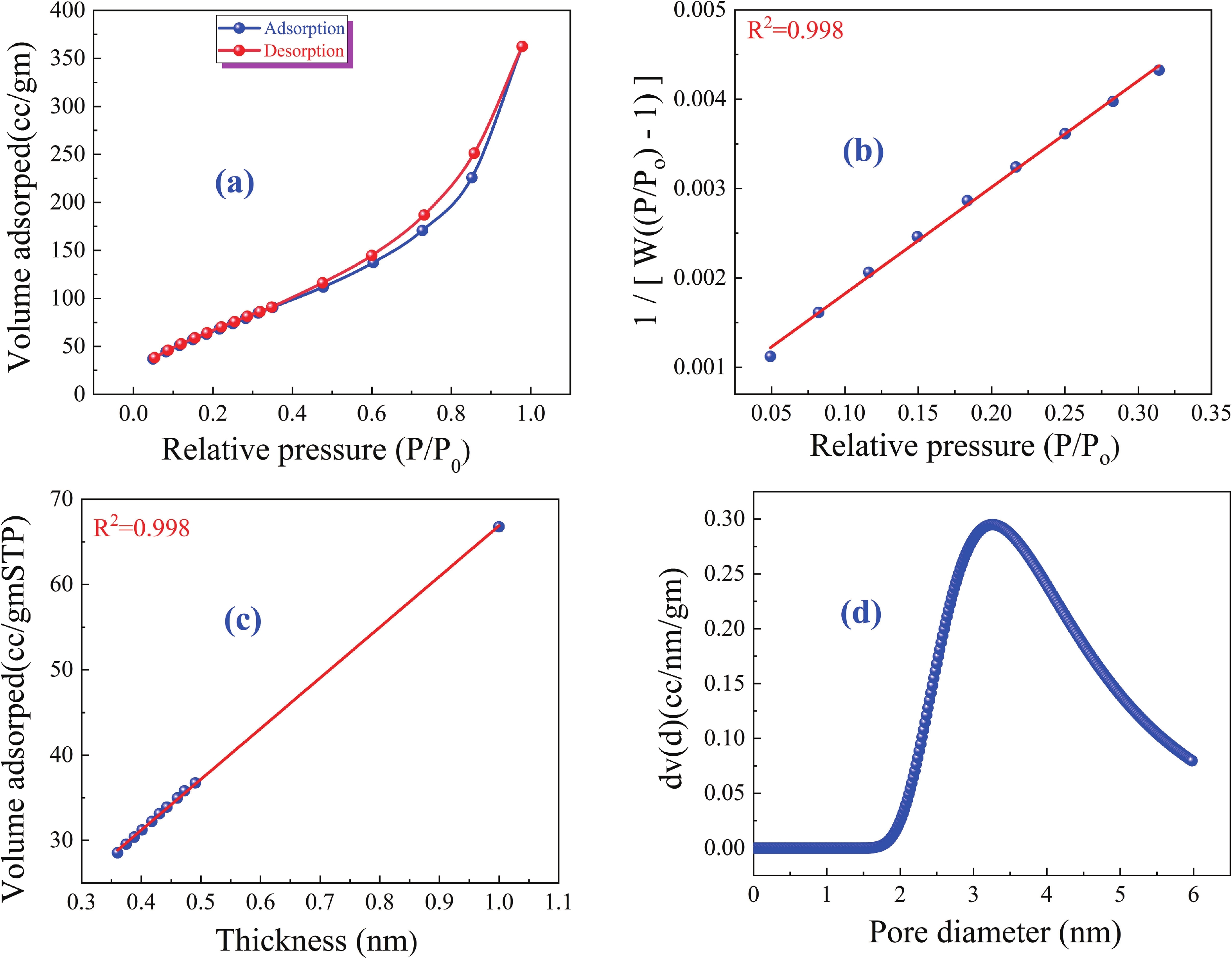
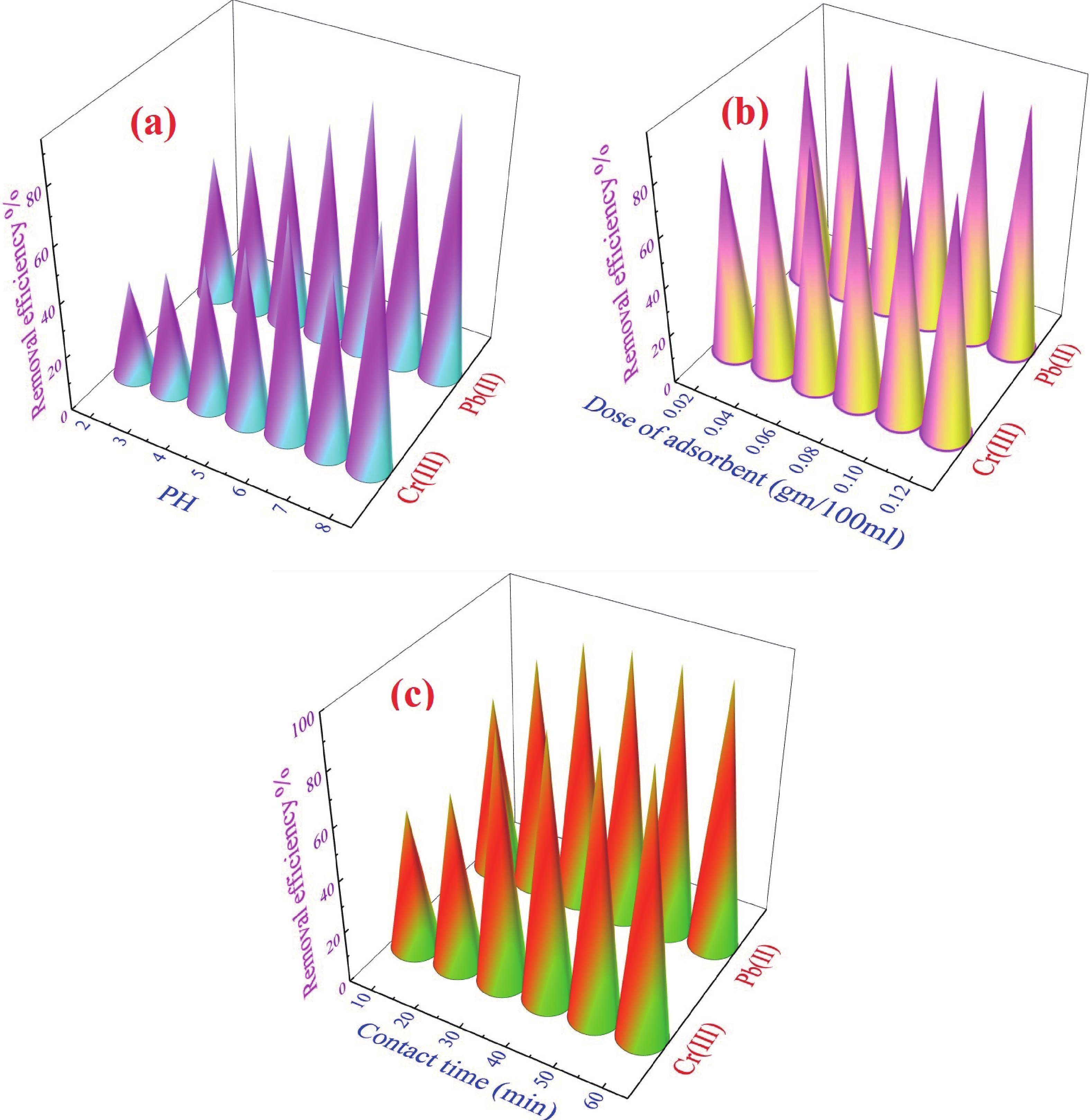
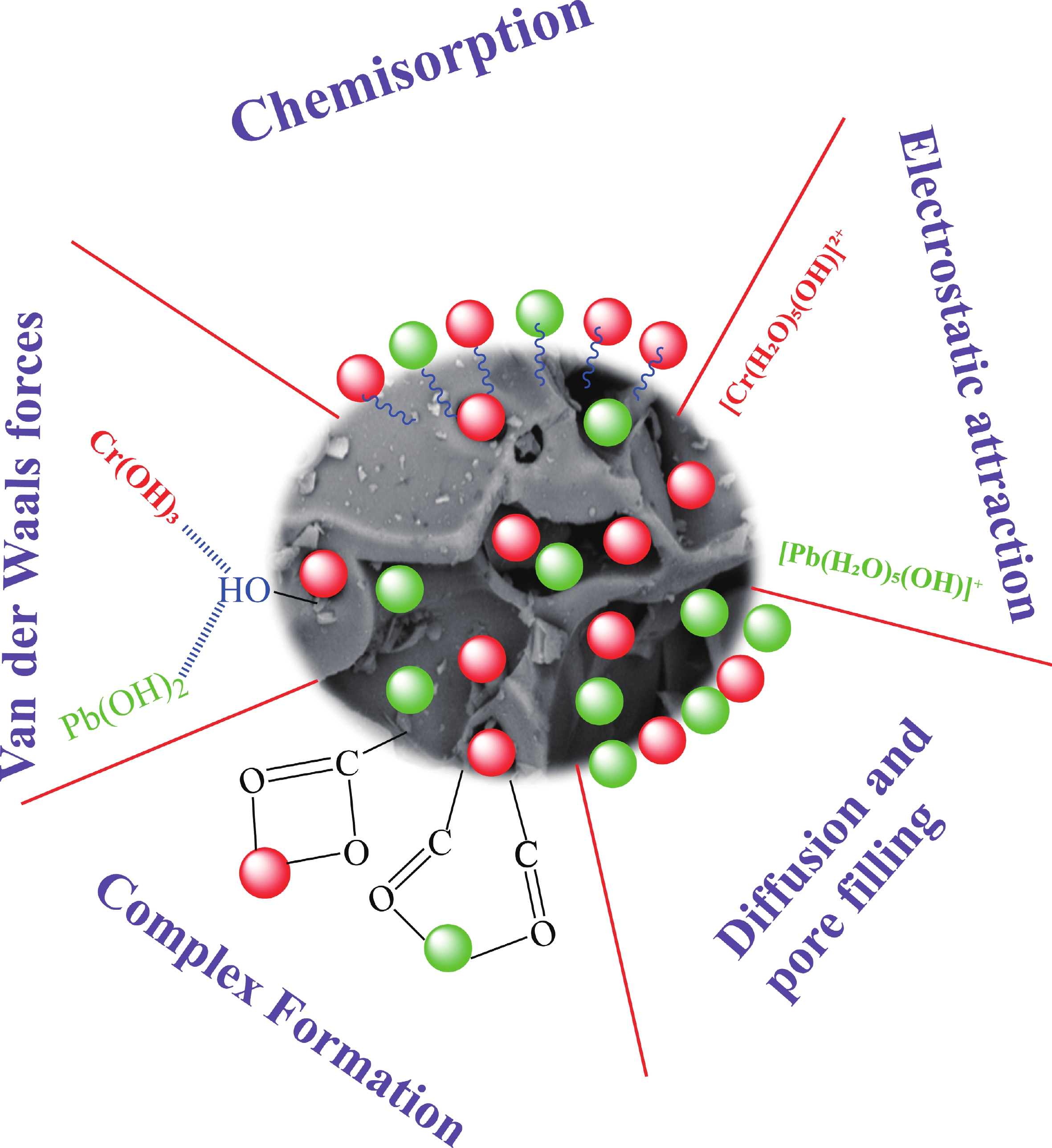
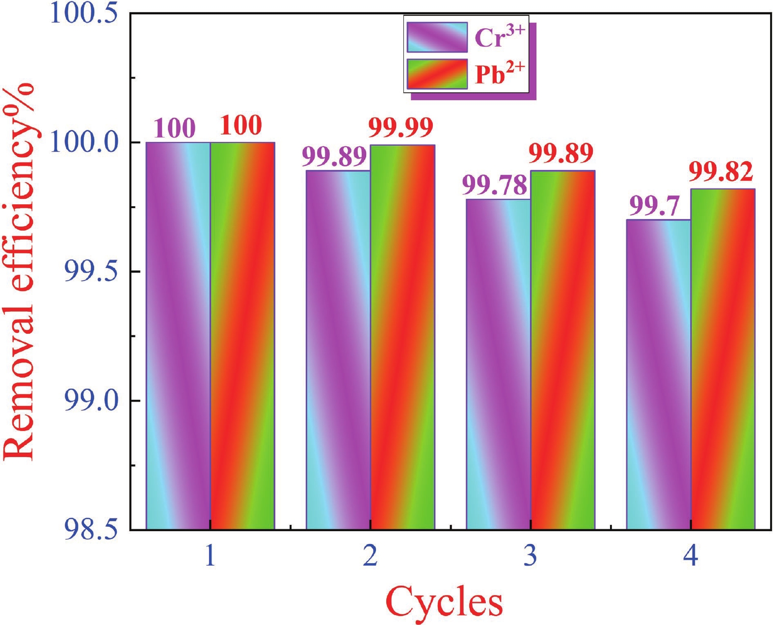
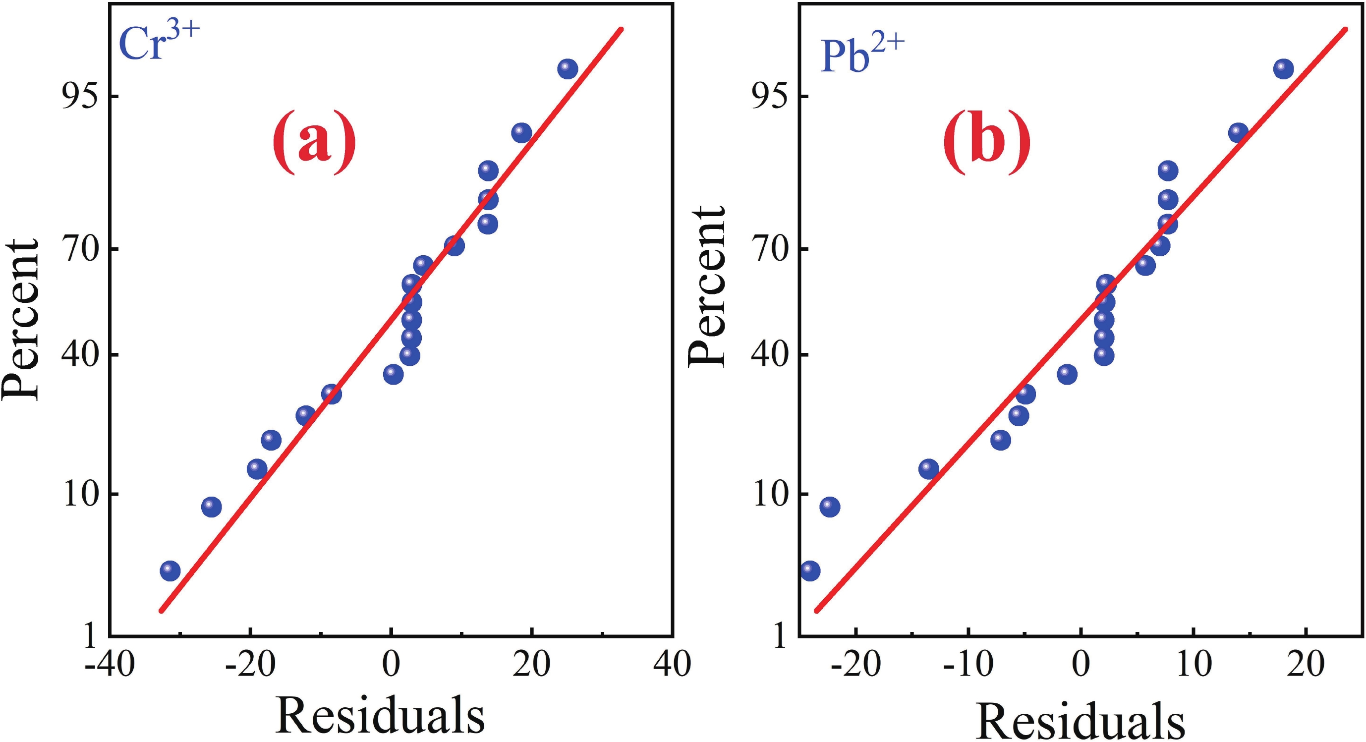
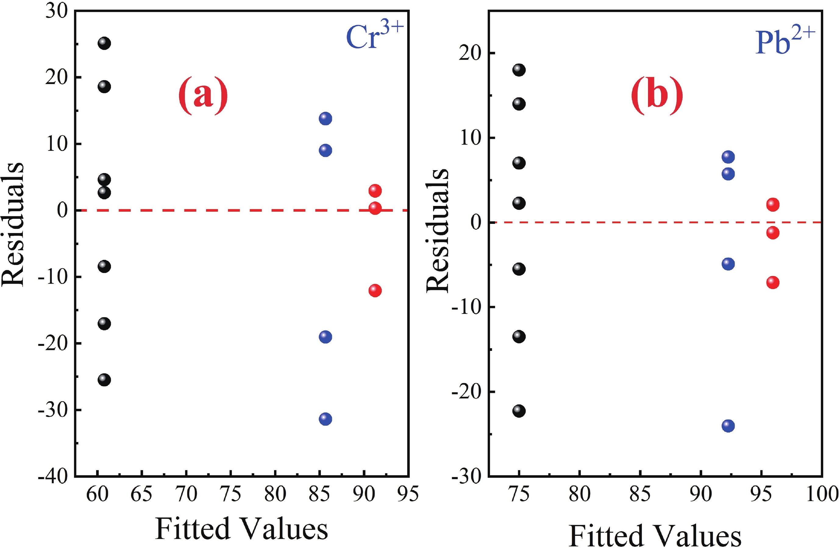
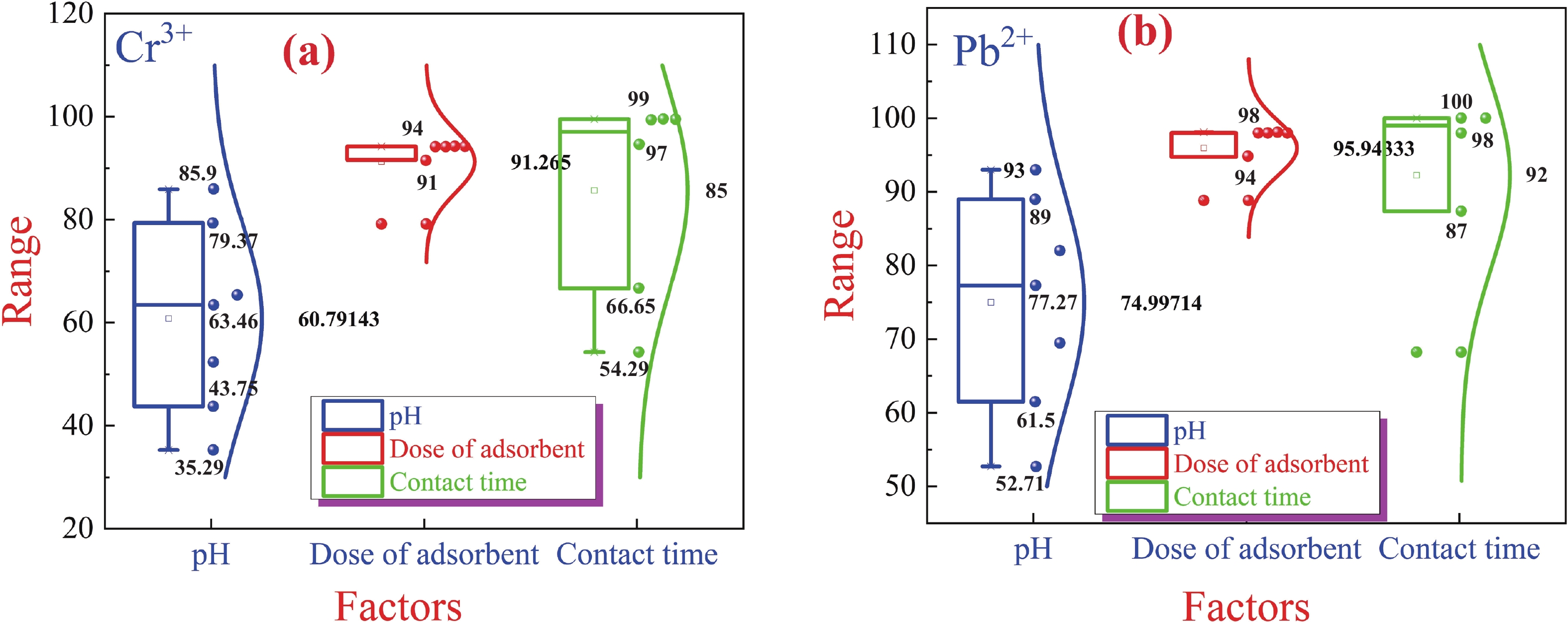
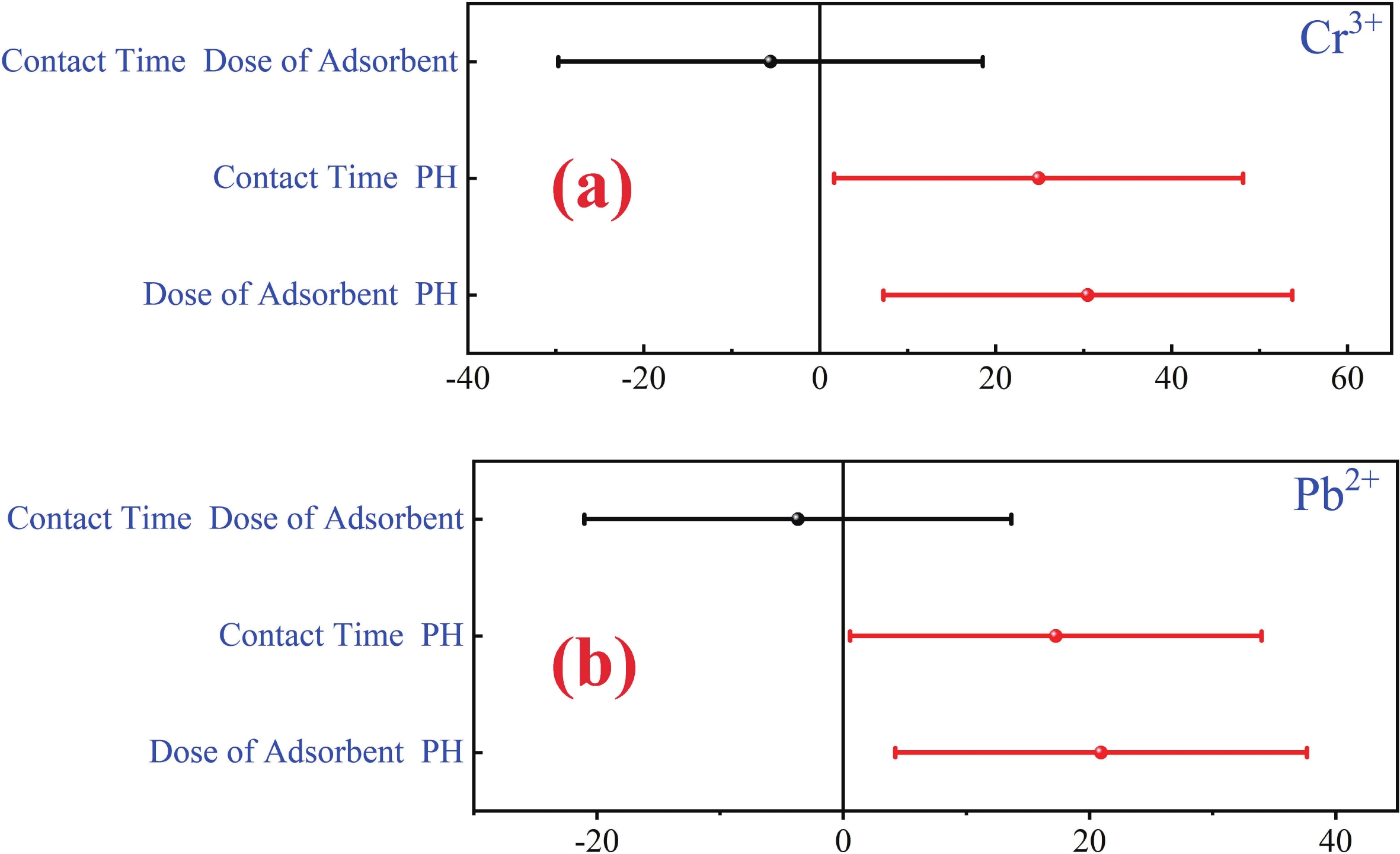
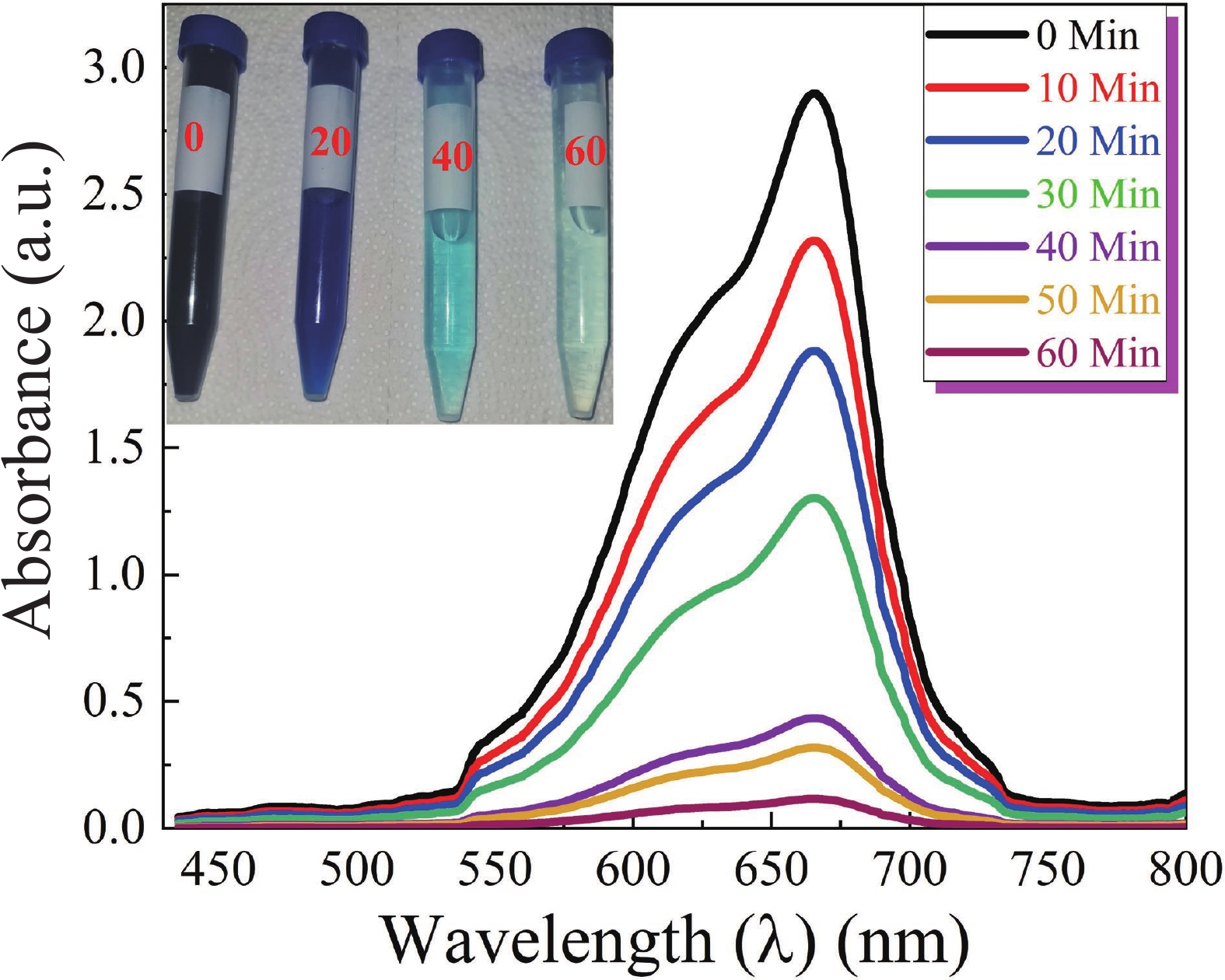
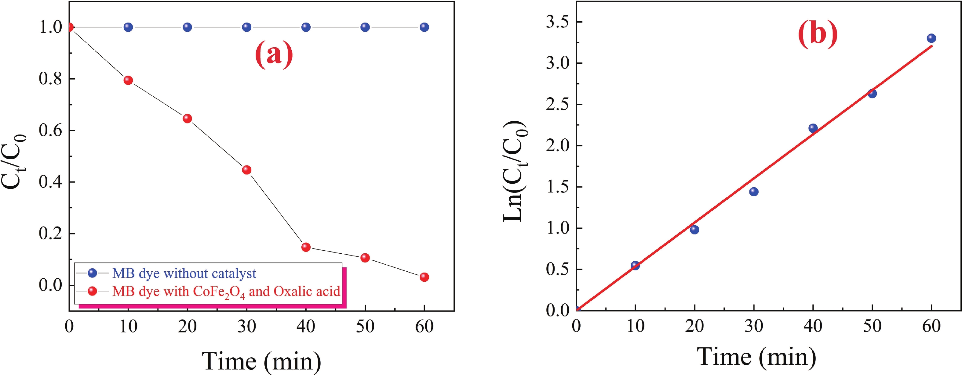
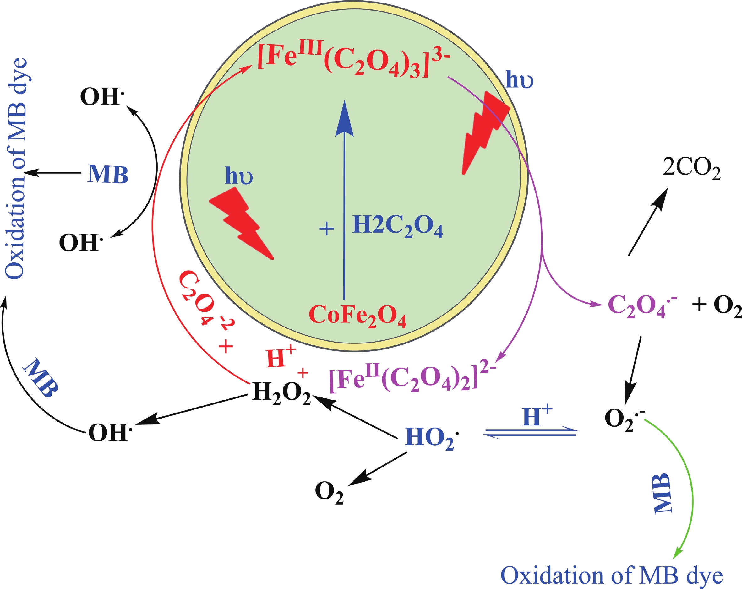
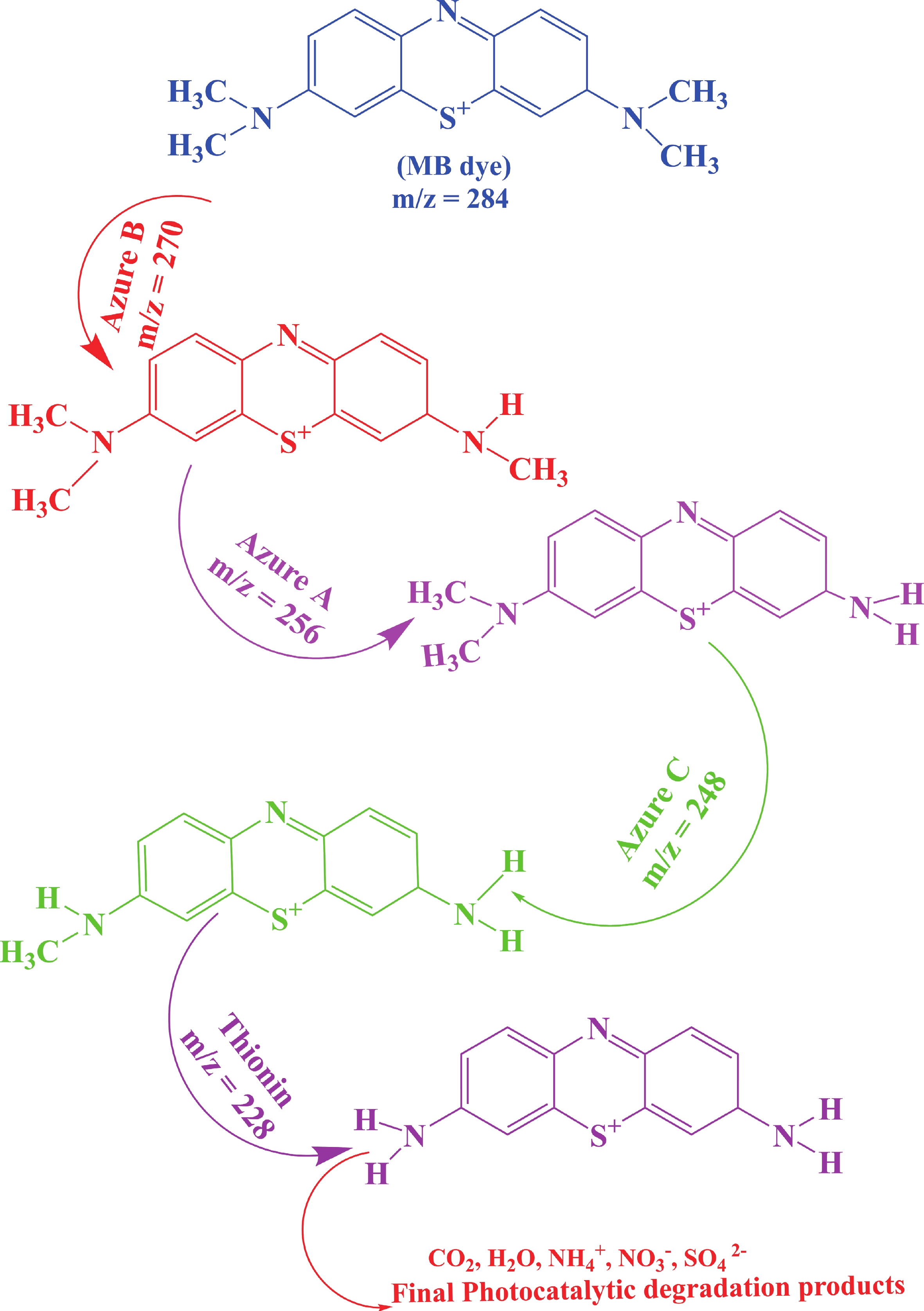
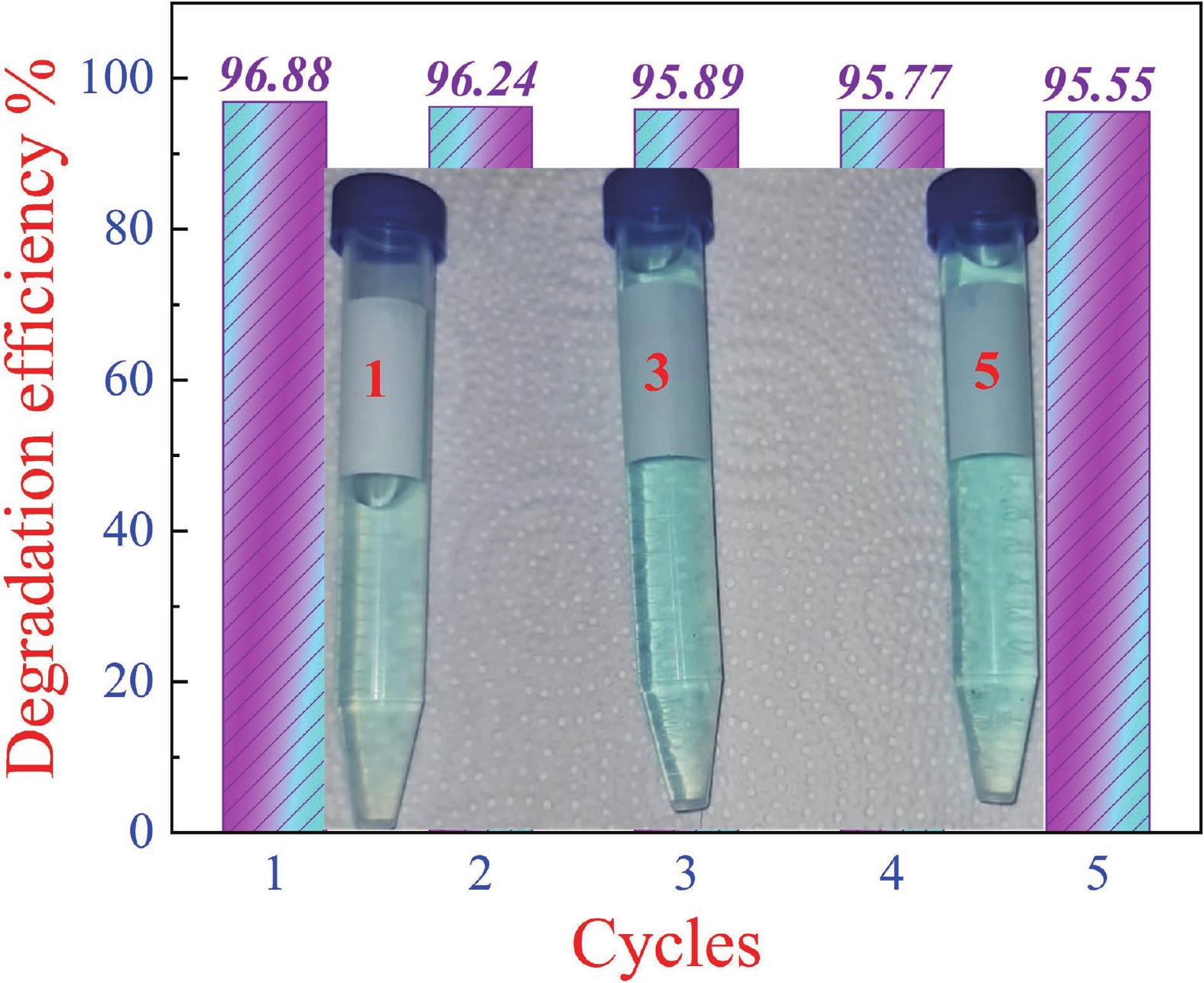
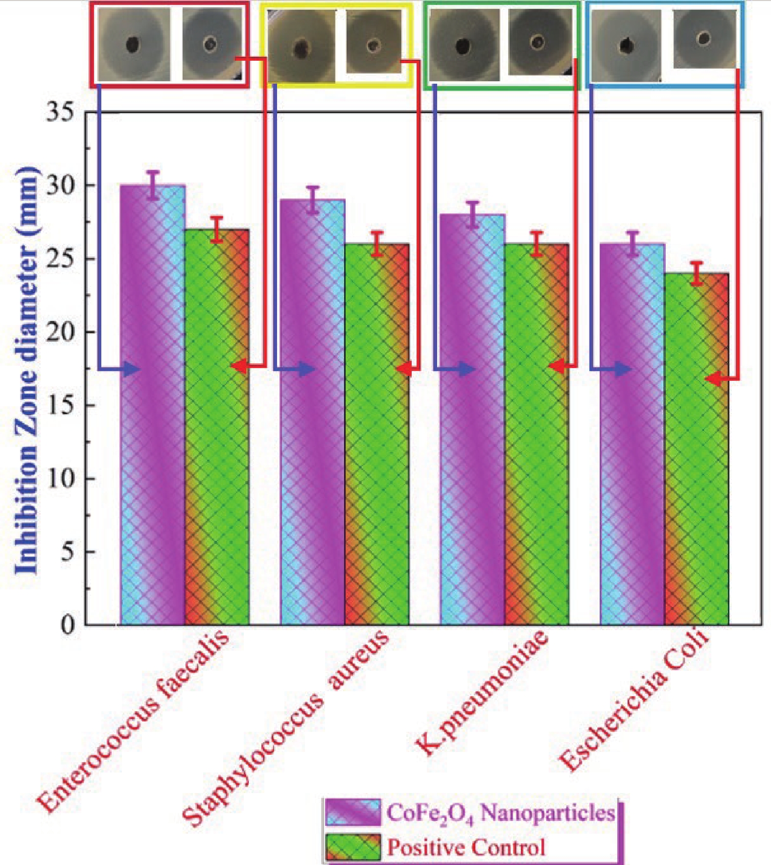
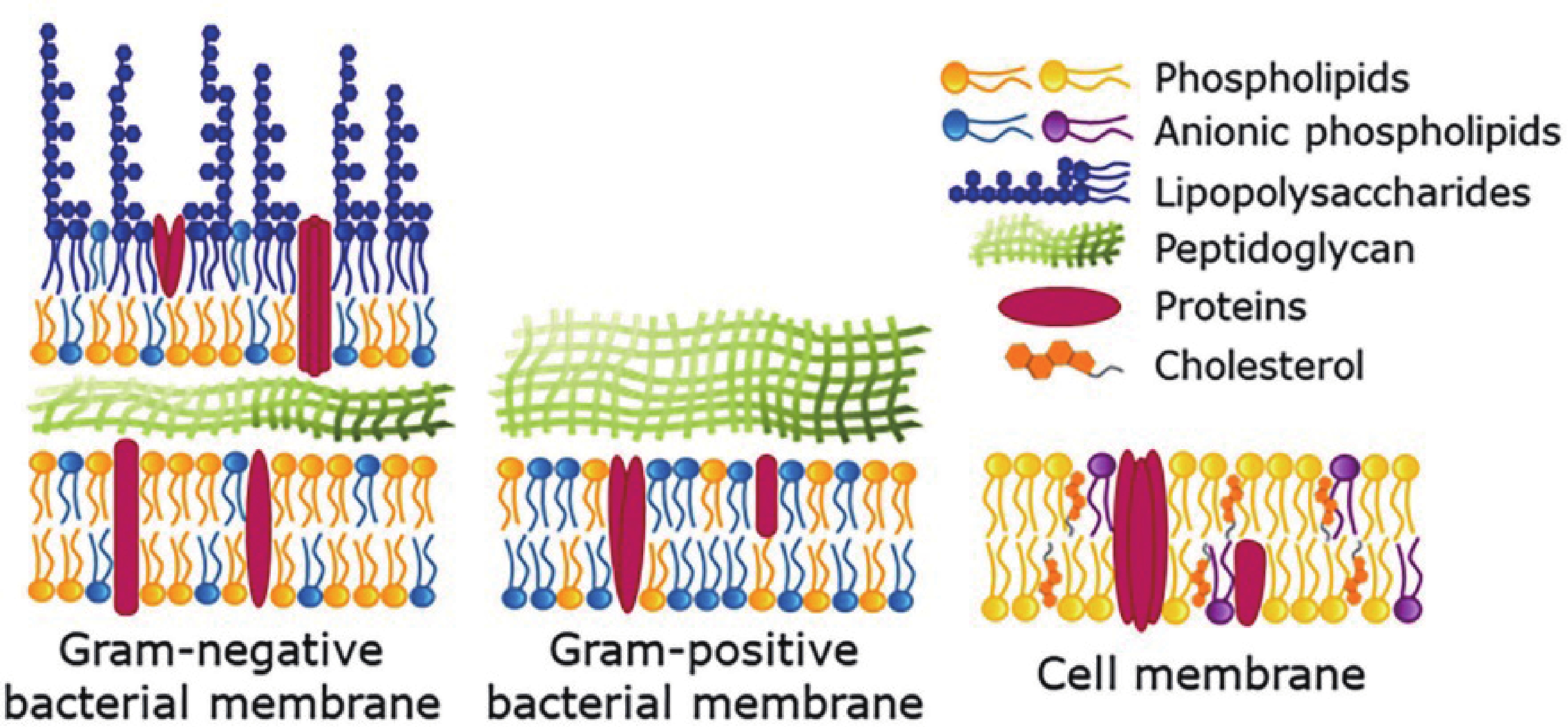
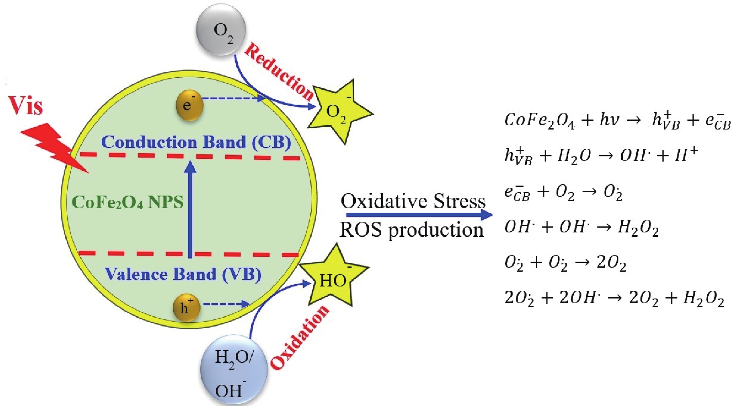
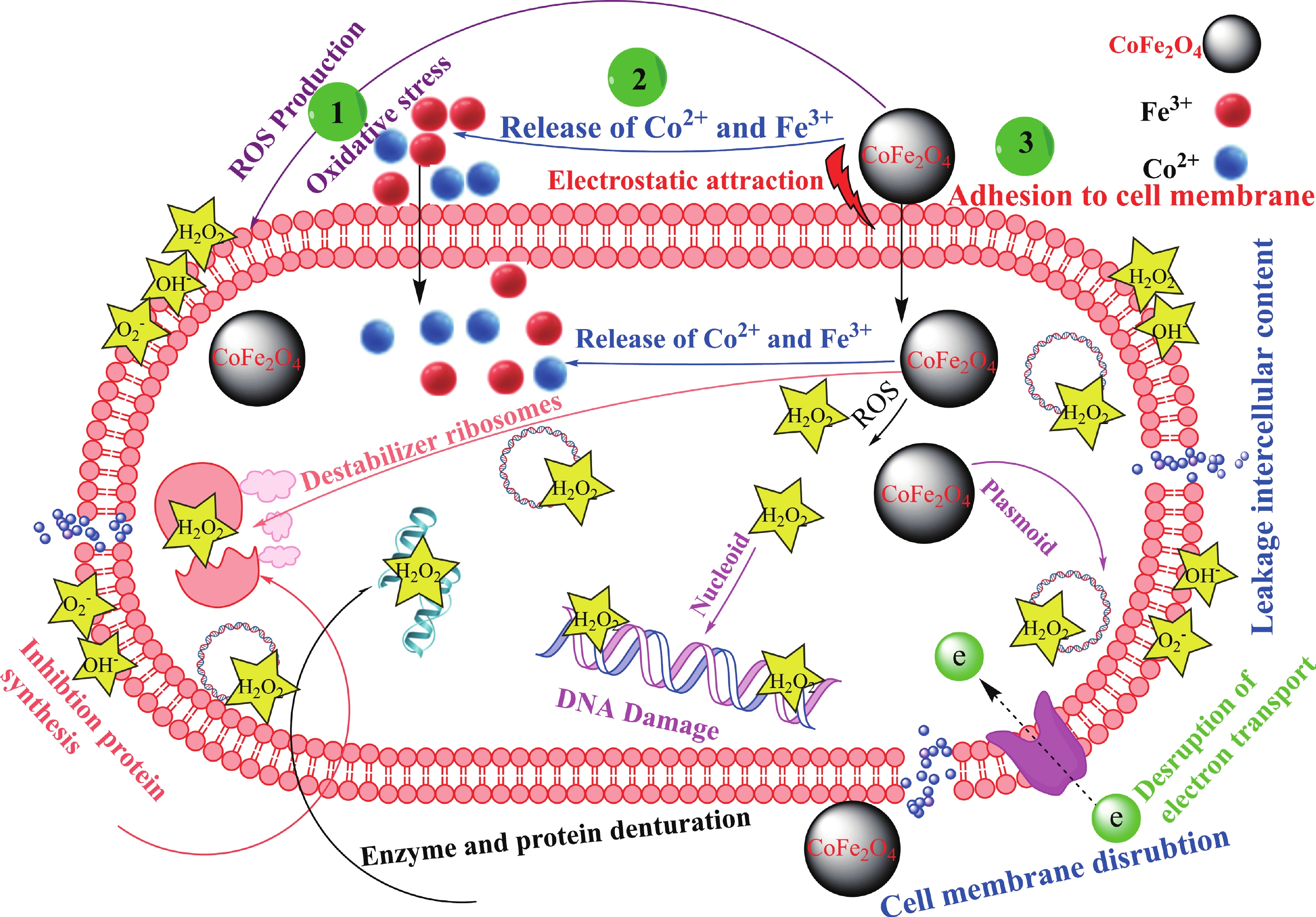
This study investigates the effect of apple extract on CoFe2O4 nanoparticles synthesized via a green self-ignition method. High resolution transmission electron microscope (HRTEM) showed nanometric particles with varied shapes, while X-ray diffraction (XRD) and Rietveld refinement confirmed a facecentered cubic (Fd3̅m) structure. Mössbauer spectroscopy revealed a Zeeman sextet pattern with only Fe3+ ions. Ultra violet vissible nearinfrared (UV–Vis–NIR) spectra indicated strong absorbance in the visible and NIR regions, suggesting optoelectronic potential. The nanoparticles demonstrated high photo-Fenton catalytic efficiency, degrading 96.88% of Methylene Blue under visible light. They also exhibited 100% adsorption capacities for Cr3+ and Pb2+, making them effective for water treatment. These properties were attributed to a large surface area (347.04 m2/g), mesoporous structure, and mixed spinel phase. ANOVA and Tukey’s honestly significant difference (HSD) tests confirmed that contact time and adsorbent dosage significantly affected pollutant removal. Additionally, strong antimicrobial activity highlighted their biotechnological relevance. The inclusion of apple extract enhanced structural and functional features, expanding application prospects in spin valves, magnetic recording, refrigeration, microwave technologies (C to Ku bands), optoelectronics, and biotechnology. Future work should explore the photo-Fenton degradation mechanism and optimize synthesis for scalable production, aiming to maximize their industrial utility.
J. Semicond.
2025, 46(12): 122301 doi: 10.1088/1674-4926/25030030
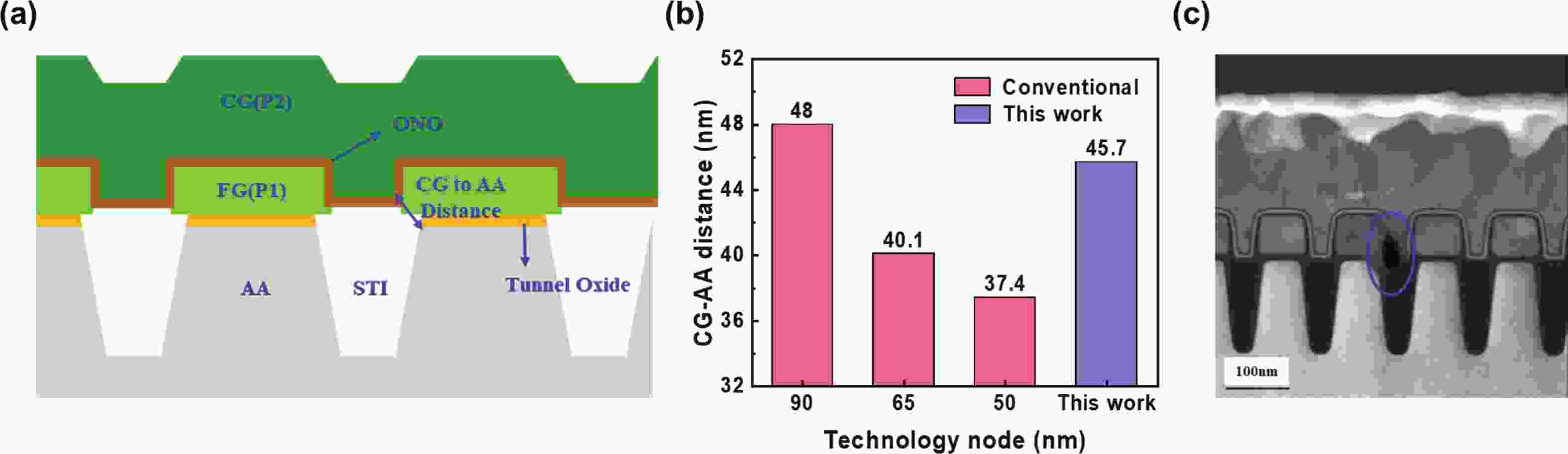
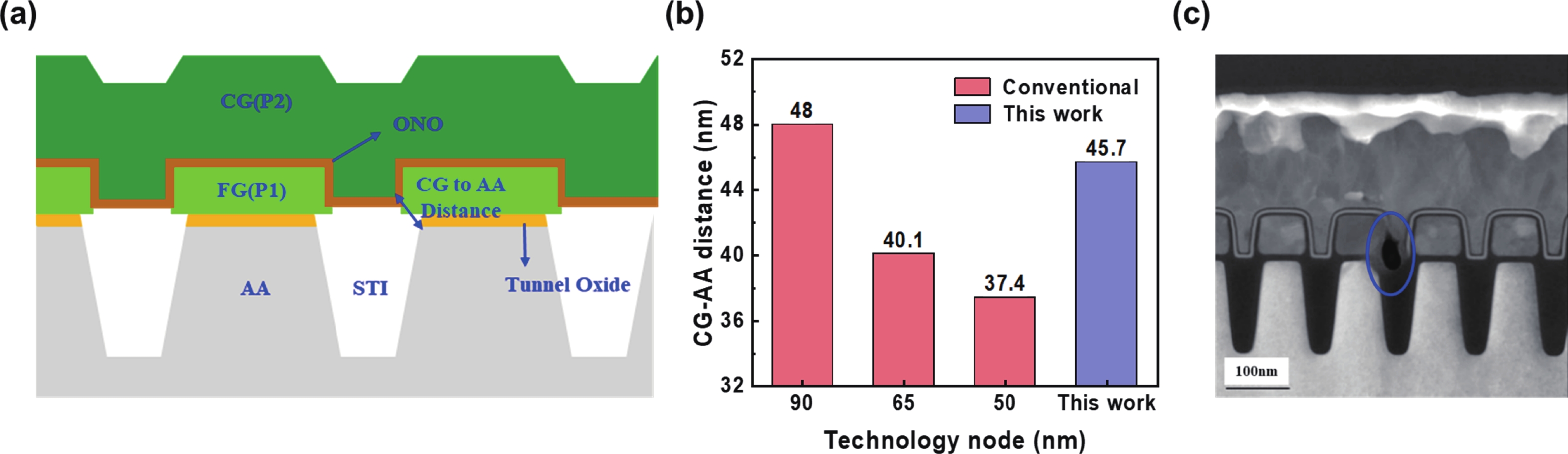
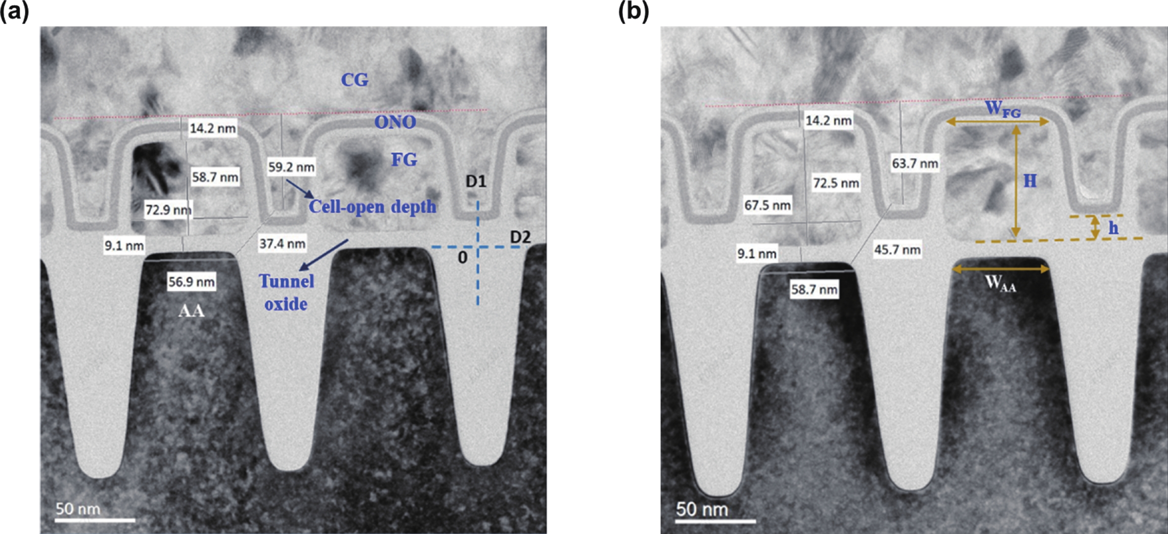
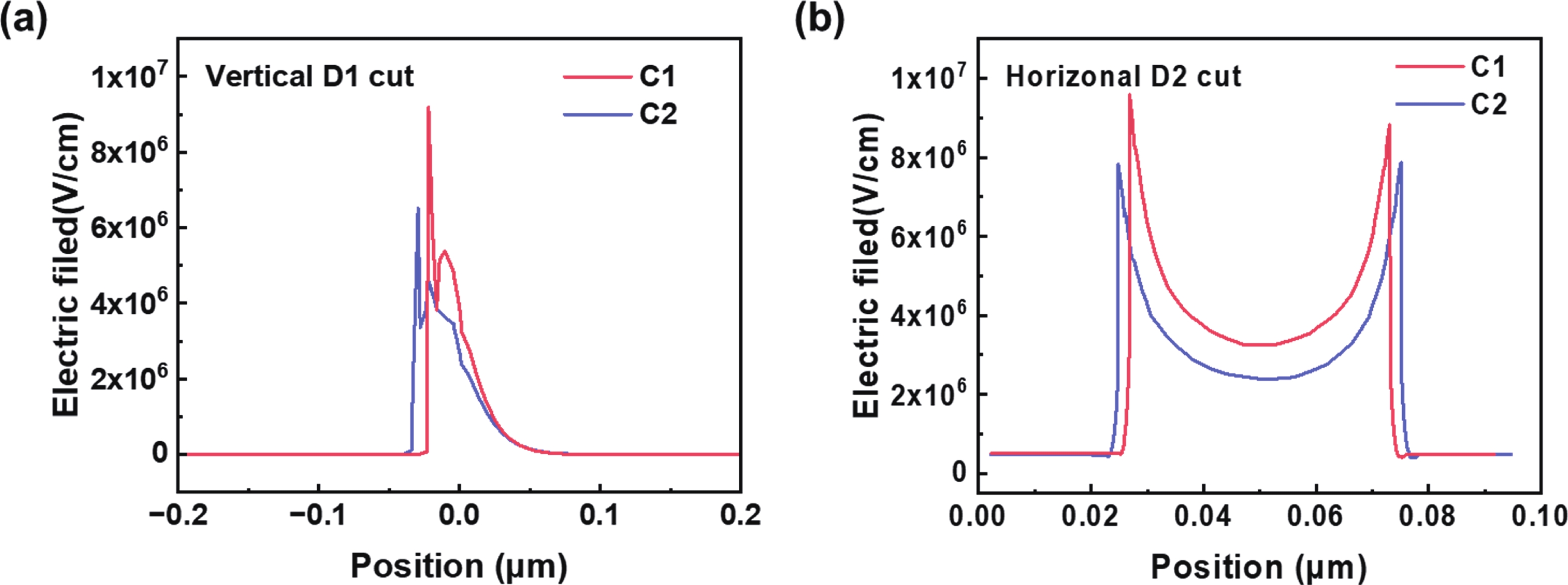
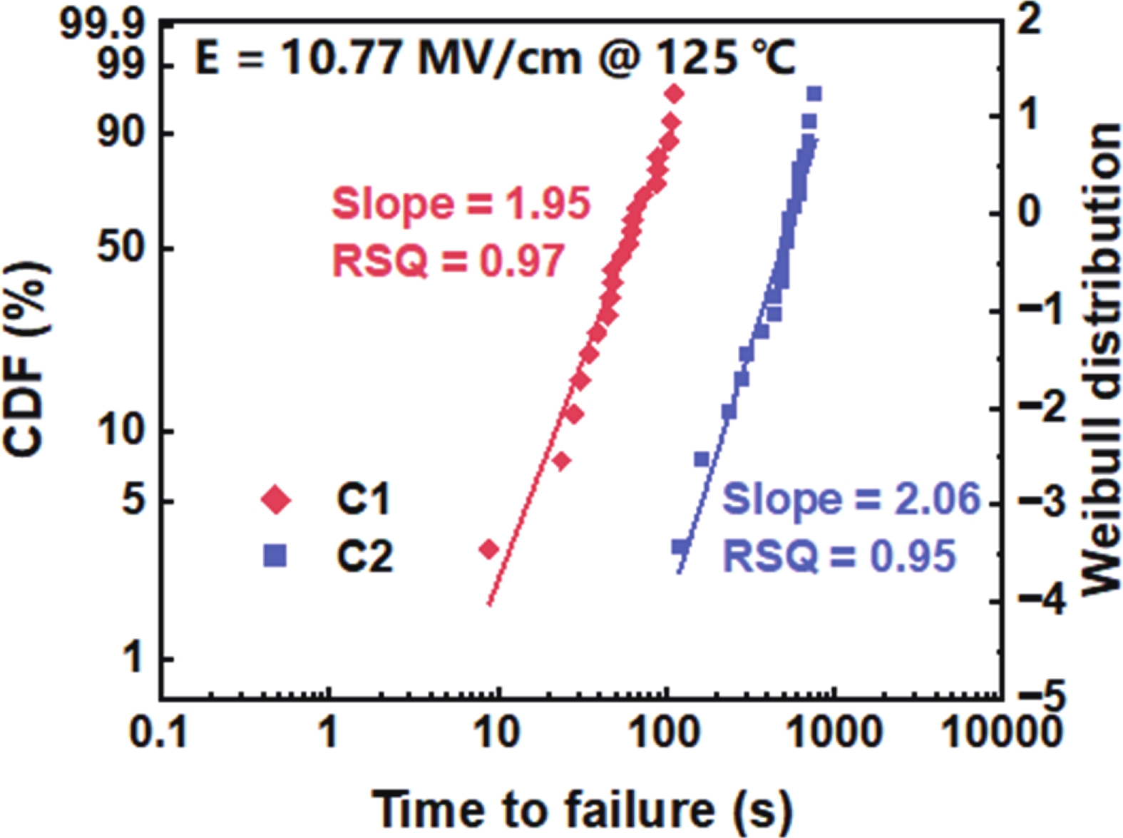
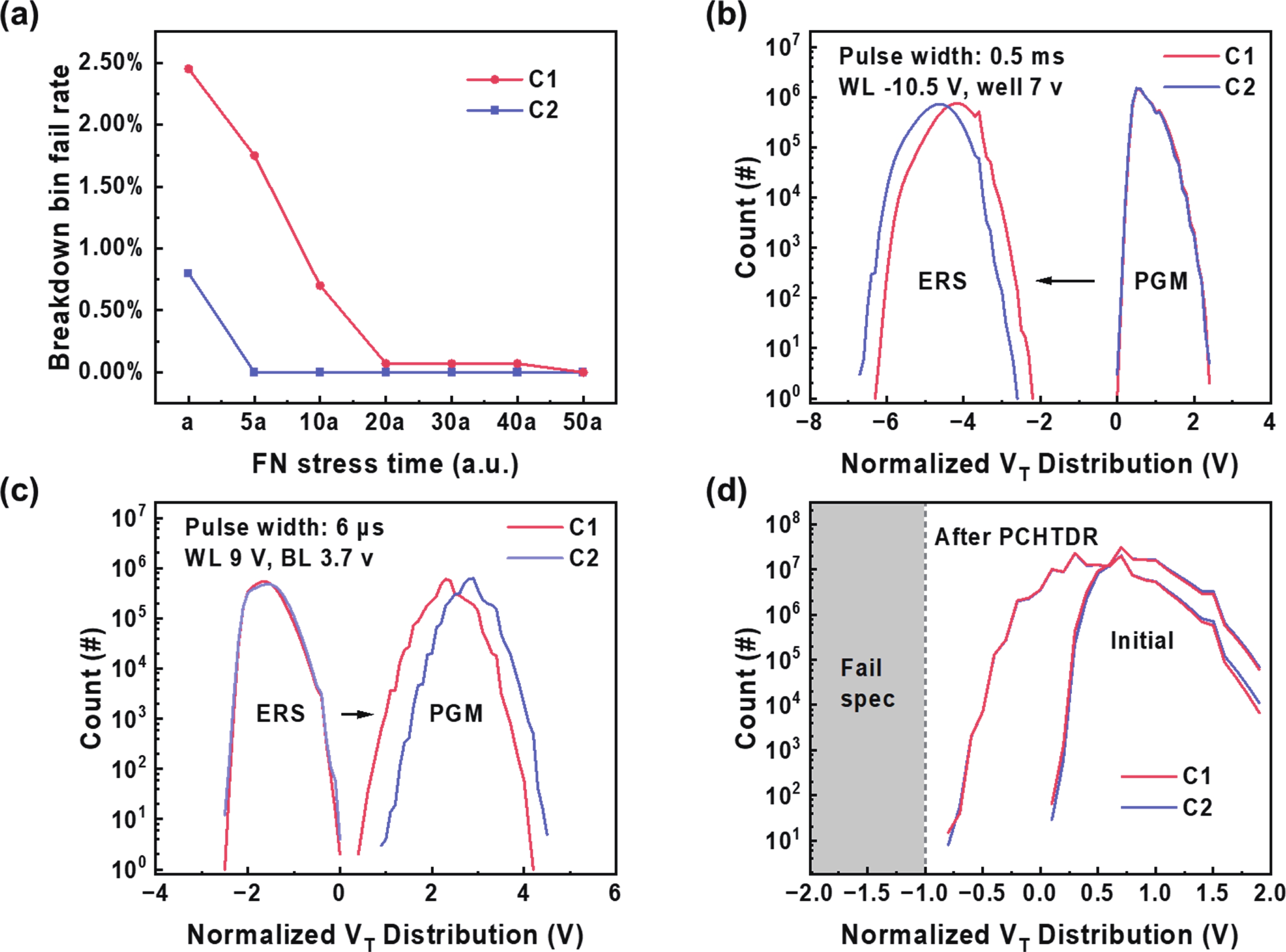
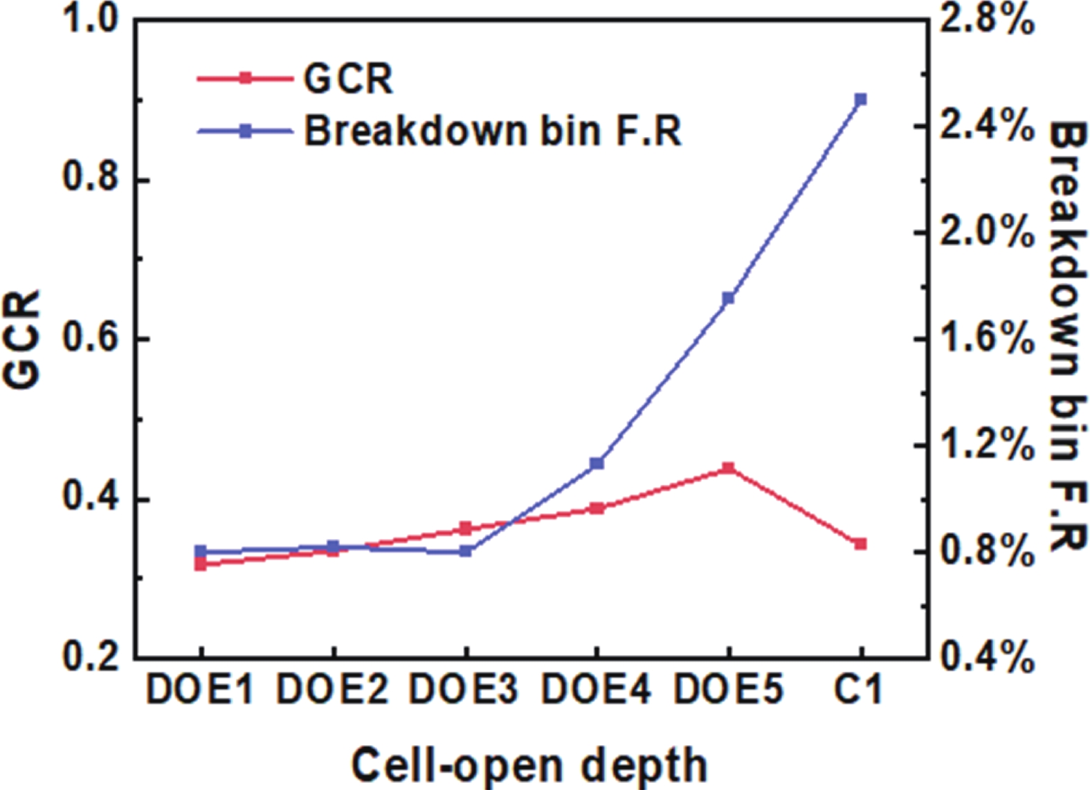
Along with NOR flash cell scaling down, dielectric burnout has gradually become one of the most important factors which affects product reliability, especially for high dropout voltage films. In this study, we demonstrate a reliability-enhanced NOR flash cell in 50 nm node technology through structural optimization of floating gate (FG) dimensions and active area profile. By synergistically increasing FG thickness, reducing FG width, and tuning cell-open depth, the control gate-to-active area corner distance expands by 22%, suppressing peak electric fields by 29% vertically and 18% horizontally. This structural innovation achieves: (1) 100× reduction in early-cycle burnout failures, (2) 7.38× time dependent dielectric breakdown lifetime improvement, while maintaining data retention and accelerating programming/erasing speeds by 15.4%/7.3%. The enhanced reliability enables 97.5% reduction in Fowler−Nordheim stress time during characterization program testing, providing a cost-effective solution for automotive-grade flash memories.
J. Semicond.
2025, 46(12): 122302 doi: 10.1088/1674-4926/25030043
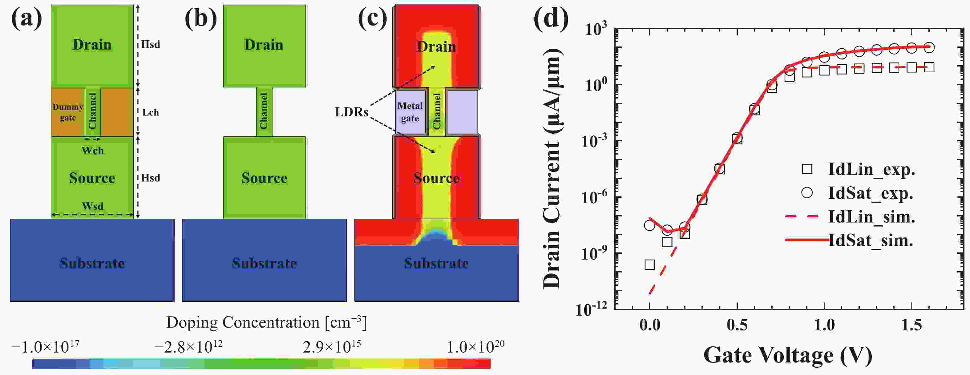
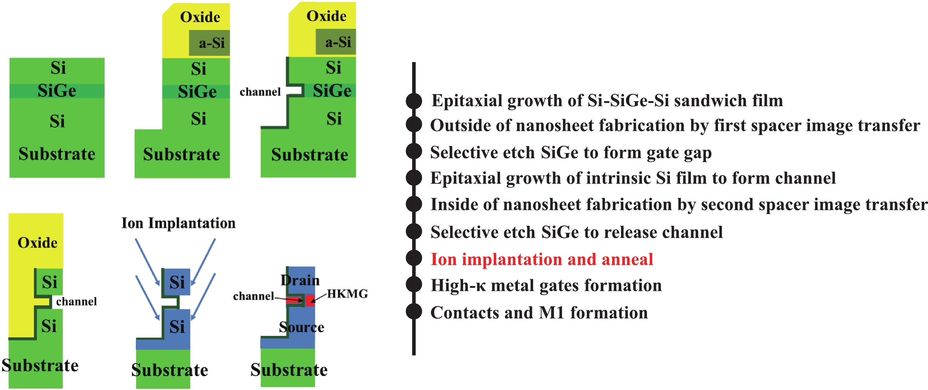
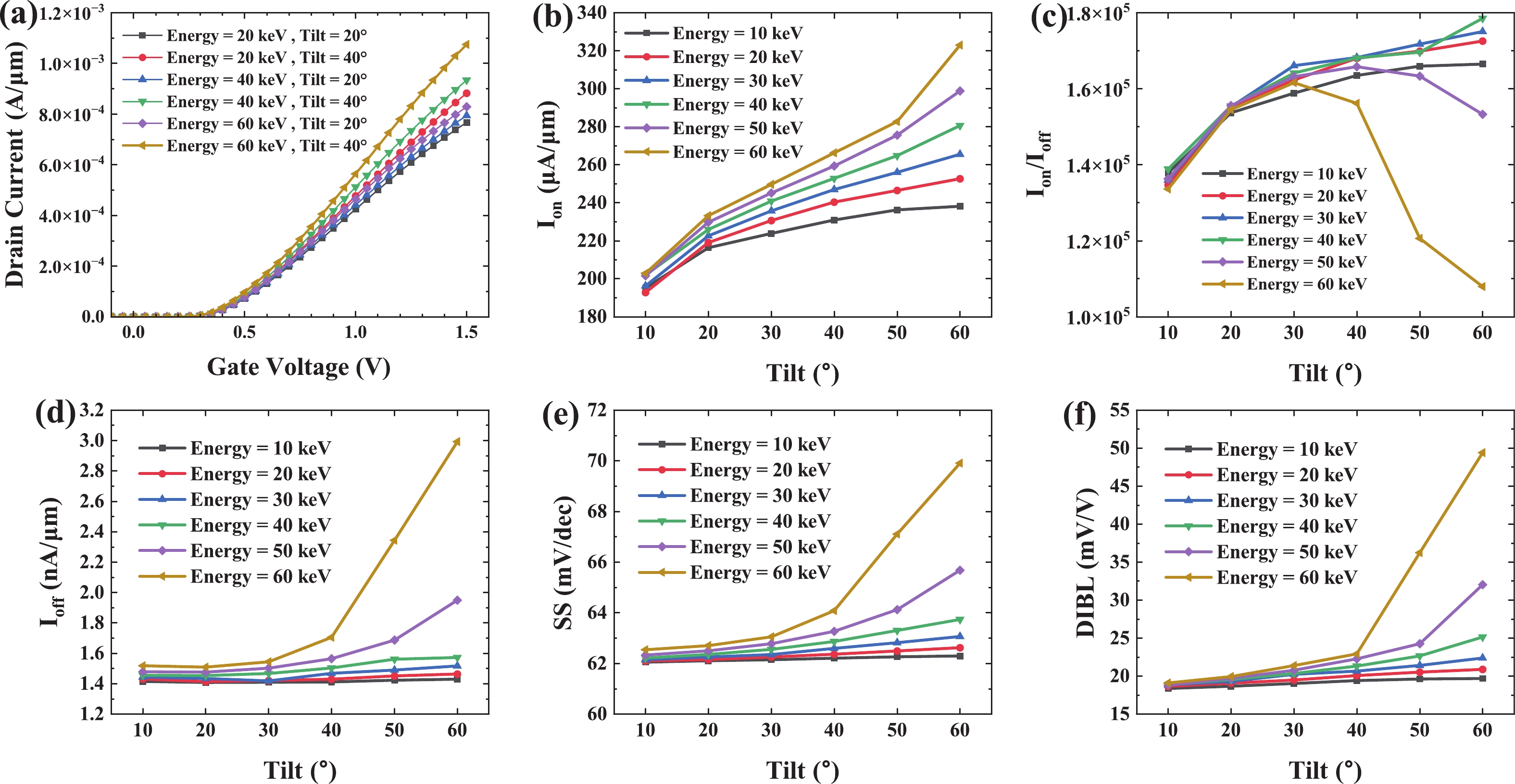
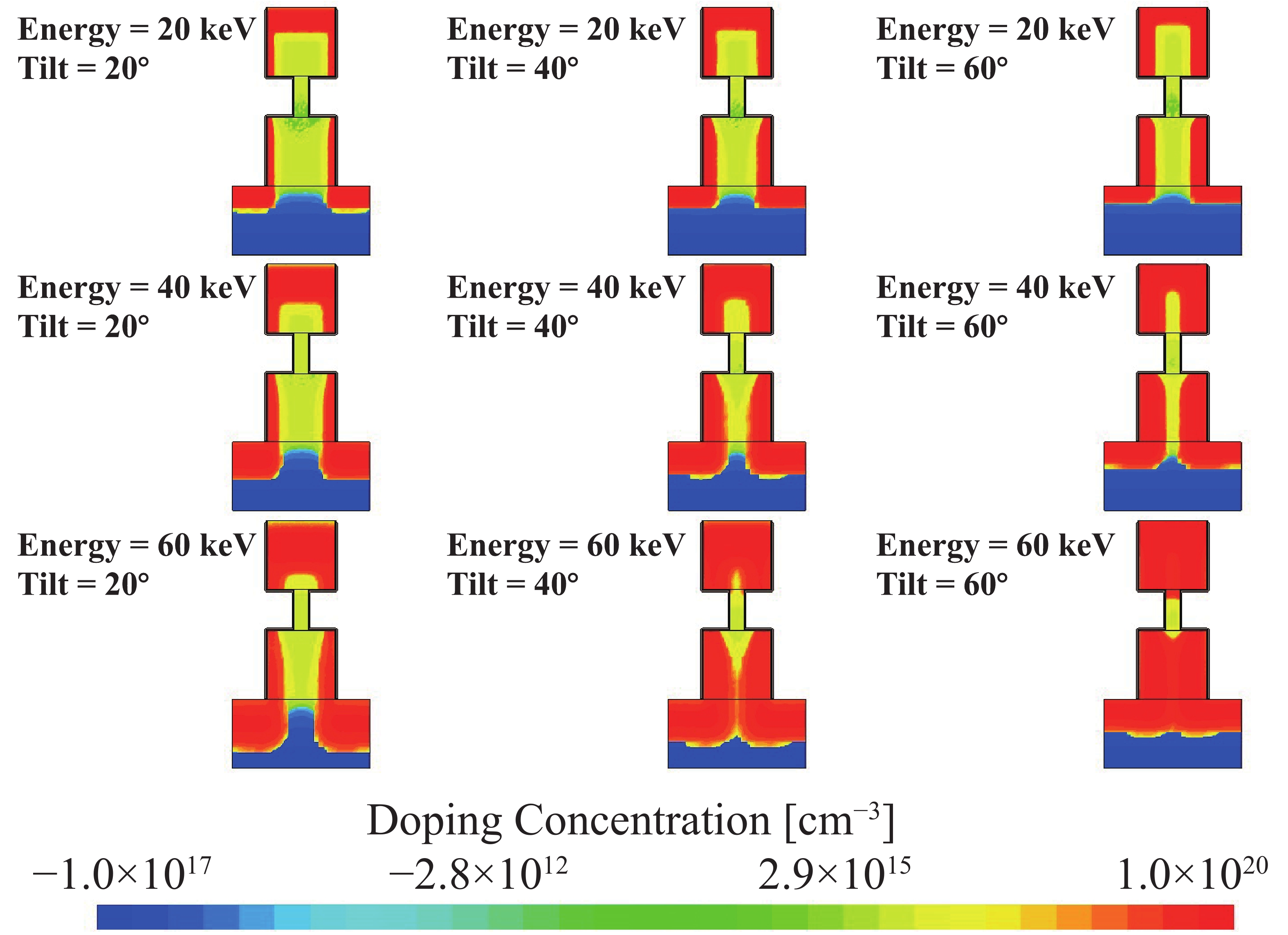
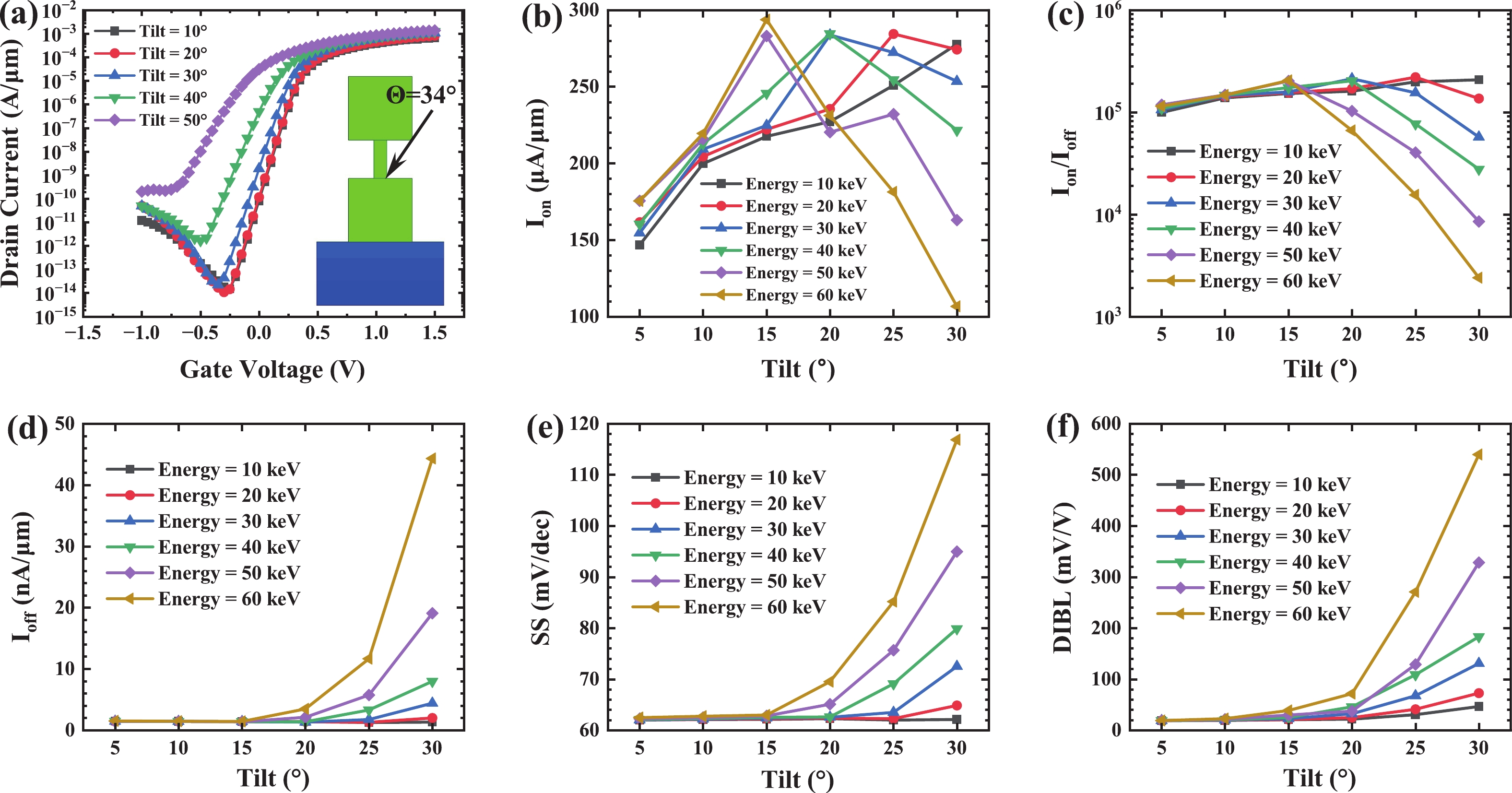
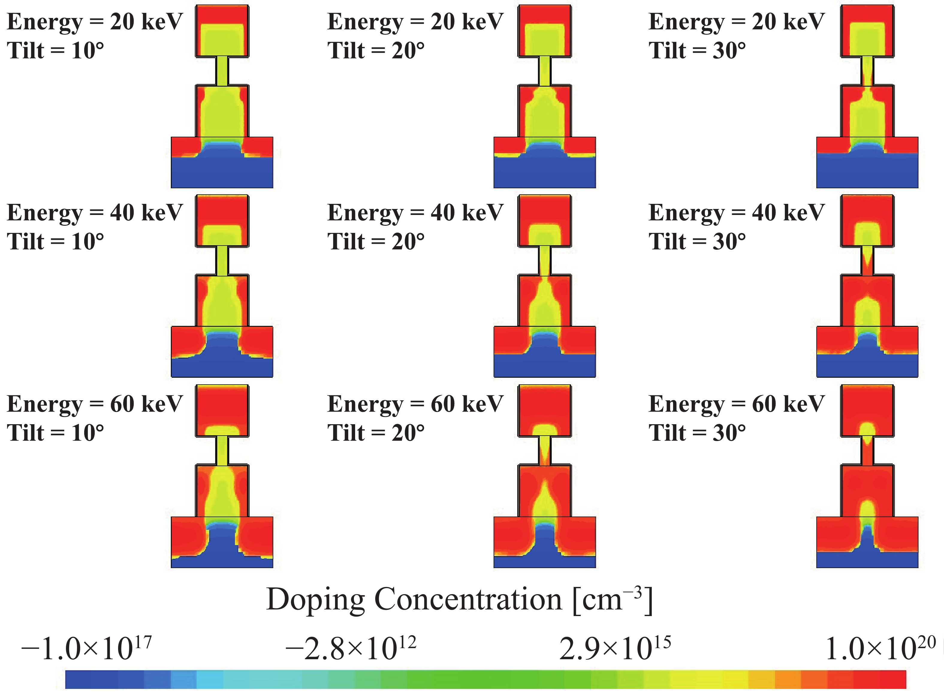
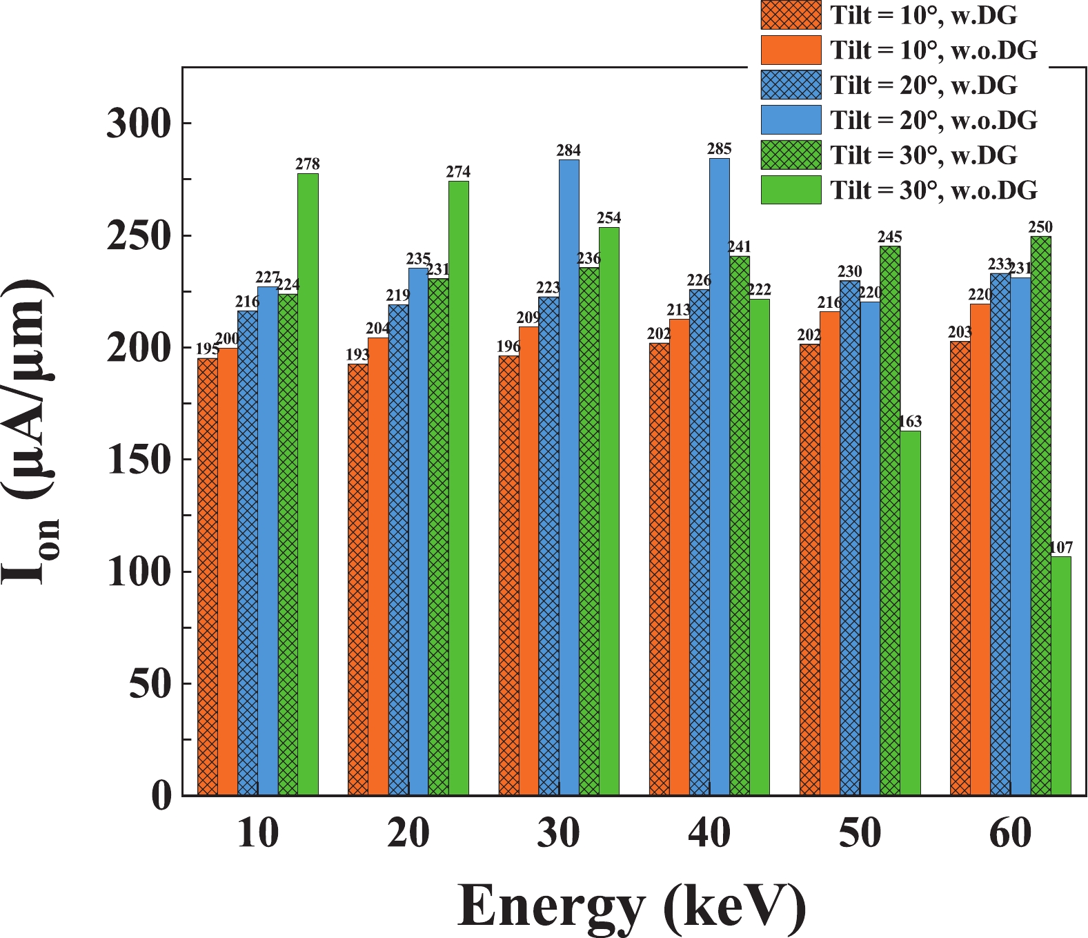
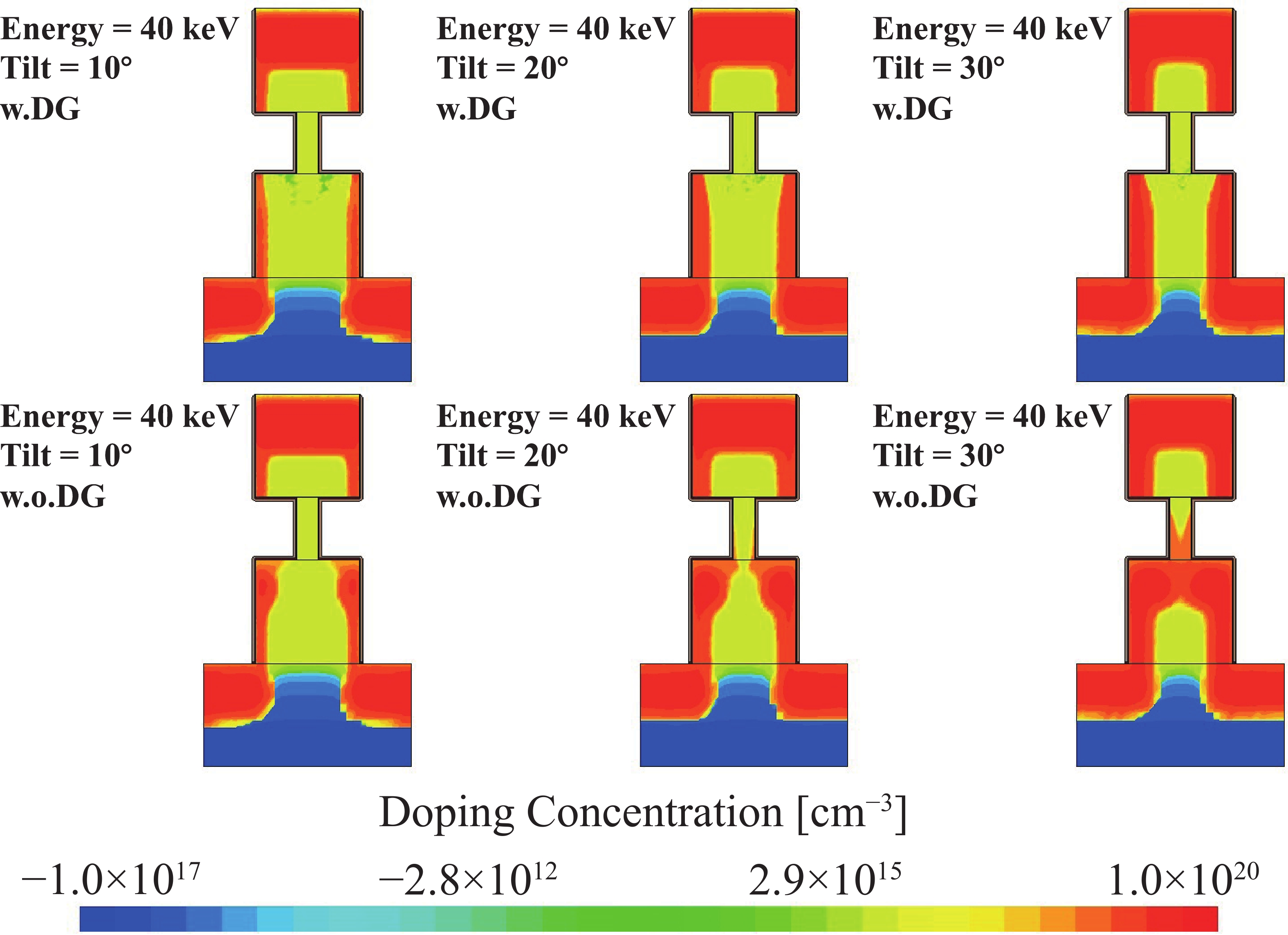
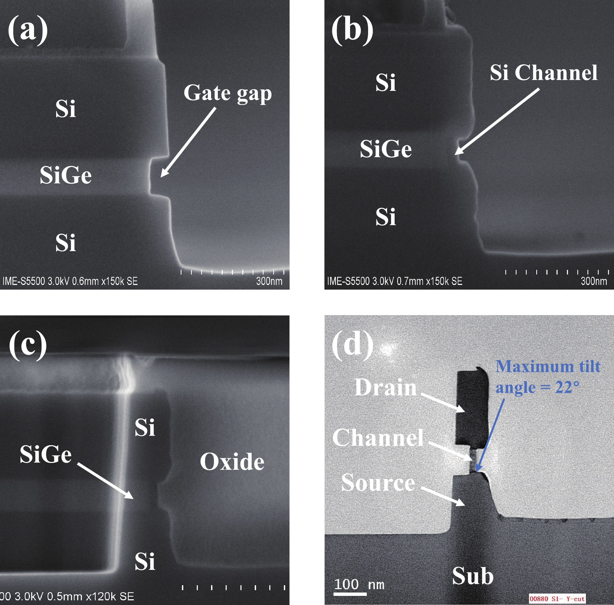
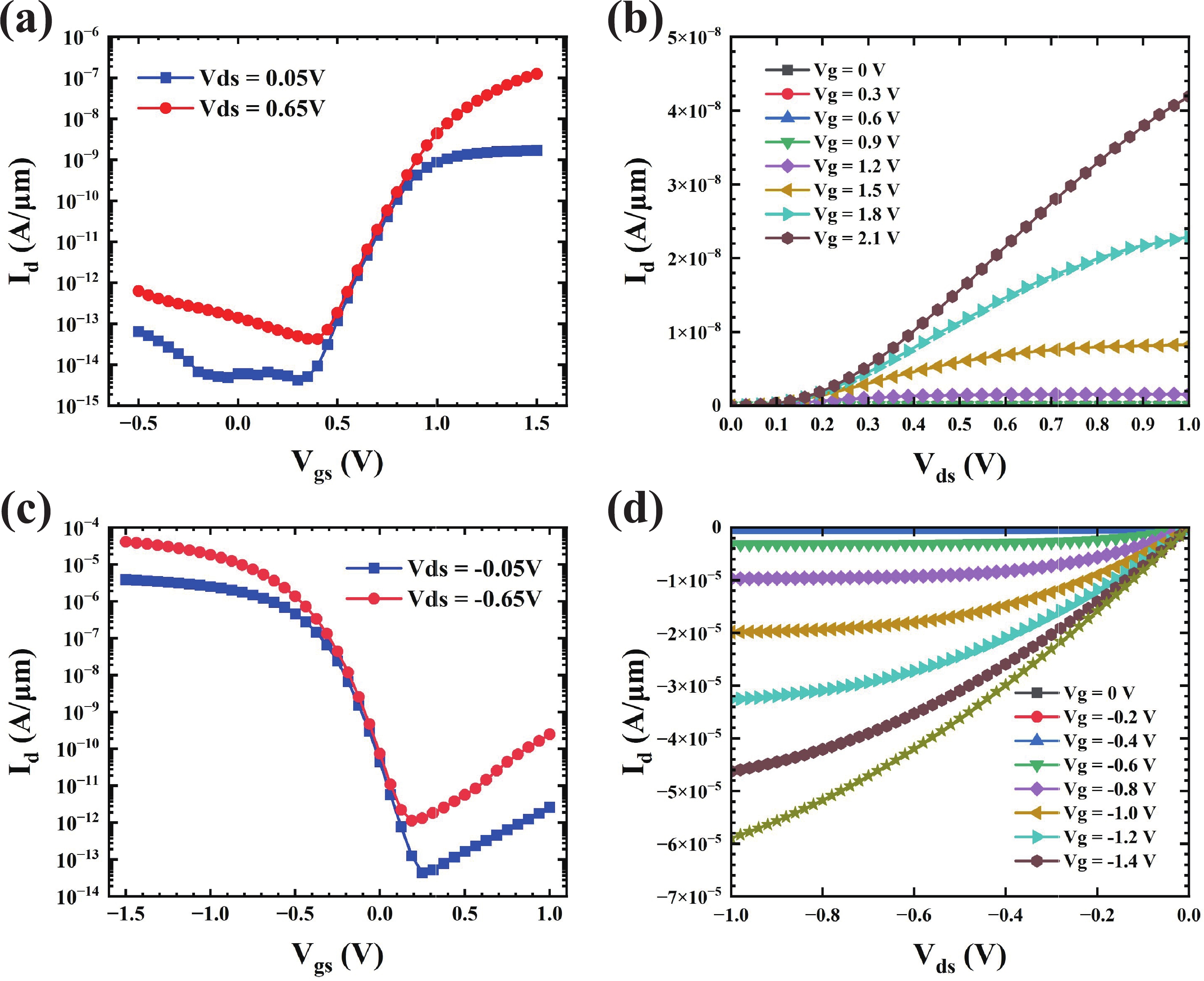
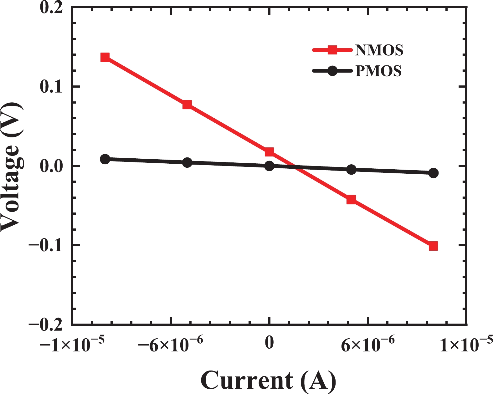
In vertical channel transistors (VCTs), source/drain ion implantation (I/I) represents a significant technical challenge due to inherent three-dimensional structural constraints, which induce complications such as difficulties in dummy gate formation and shadowing effects of I/I. This article systematically investigates the impact of different implantation conditions on the performance of VCTs with and without dummy gates through TCAD simulation. It reveals the significant role of the lightly doped regions (LDRs) naturally formed due to ion implantation in source/drain of VCTs. Furthermore, it was found that VCT without dummy gates can achieve an approximately 27% increase in on-state current (Ion) under the same implantation conditions, and can greatly simplify the process flow and reduce costs. Finally, N-type and P-type VCTs were successfully fabricated using this implantation method.
J. Semicond.
2025, 46(12): 122401 doi: 10.1088/1674-4926/25030031
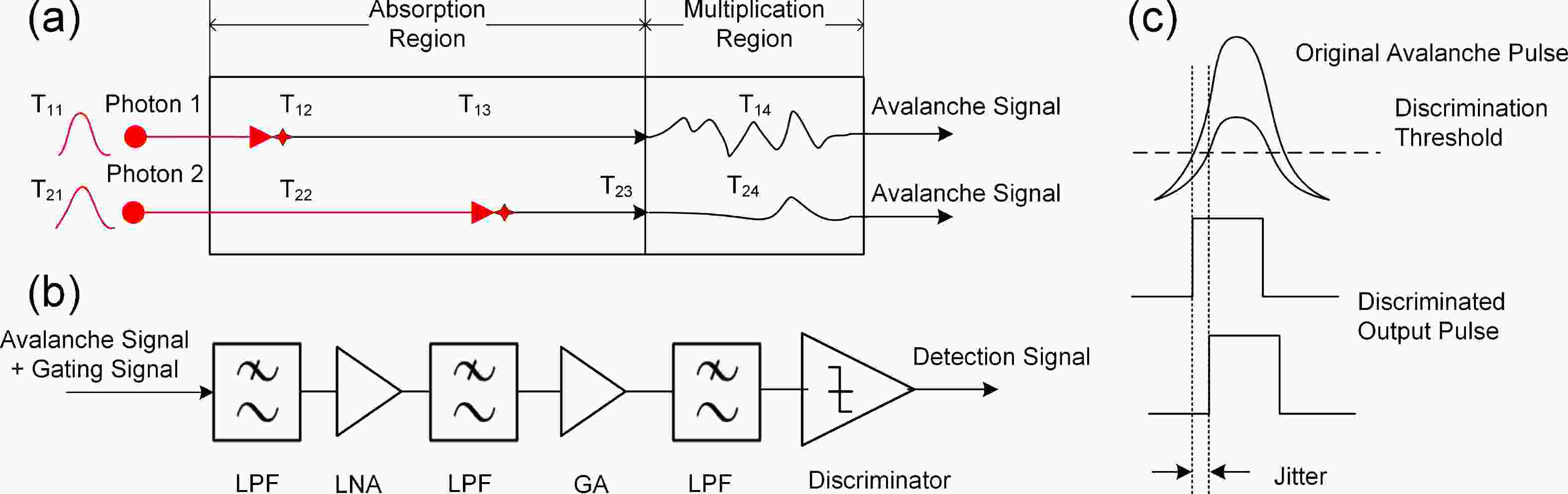
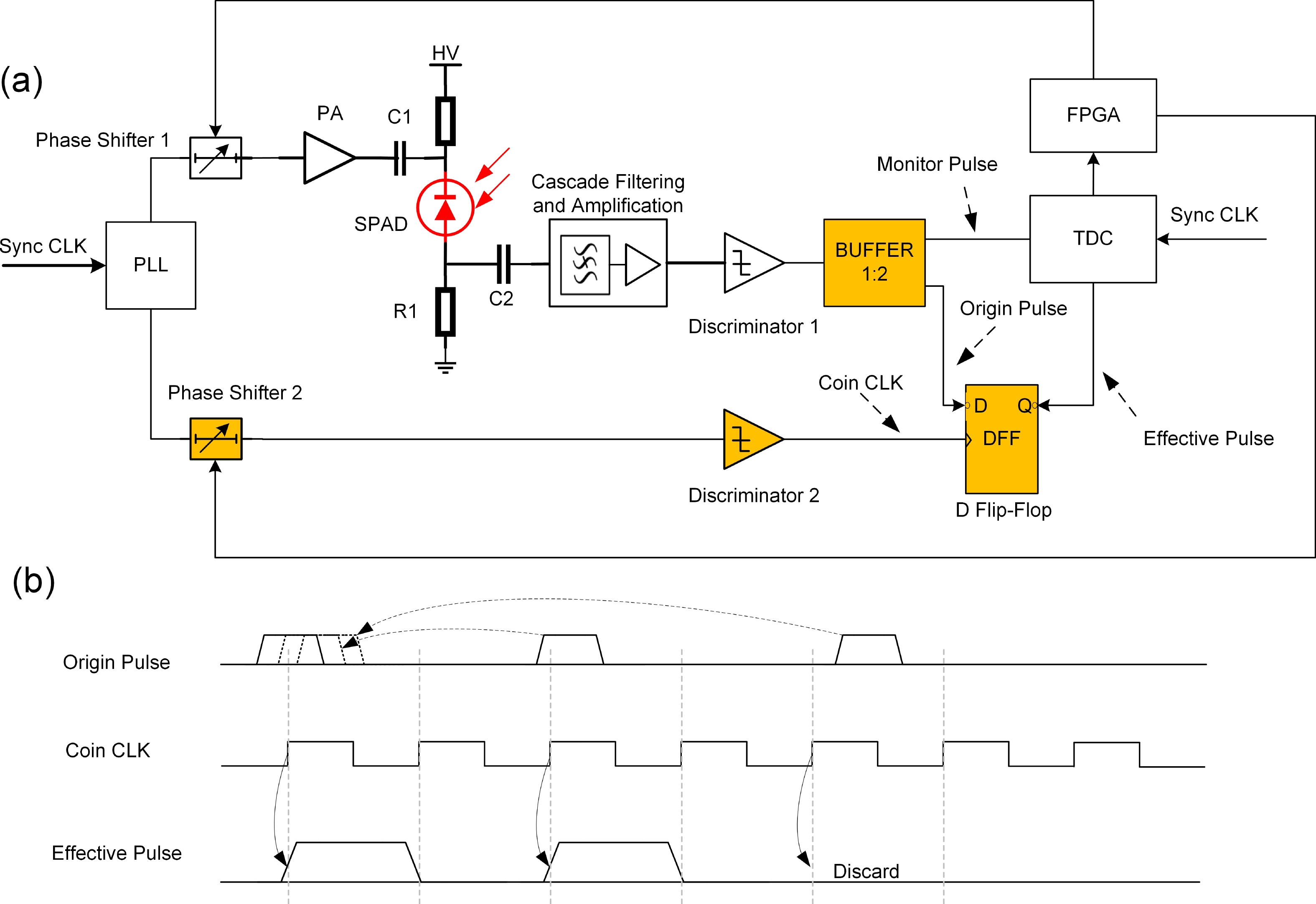
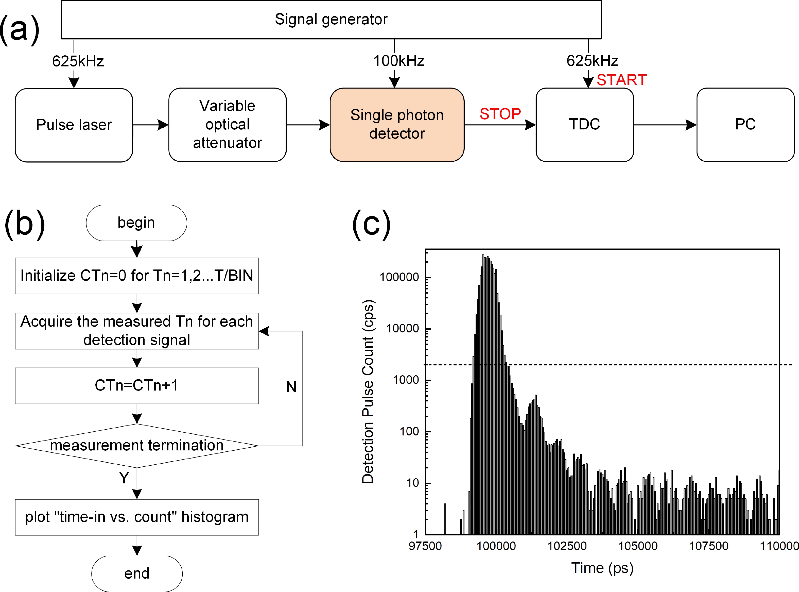
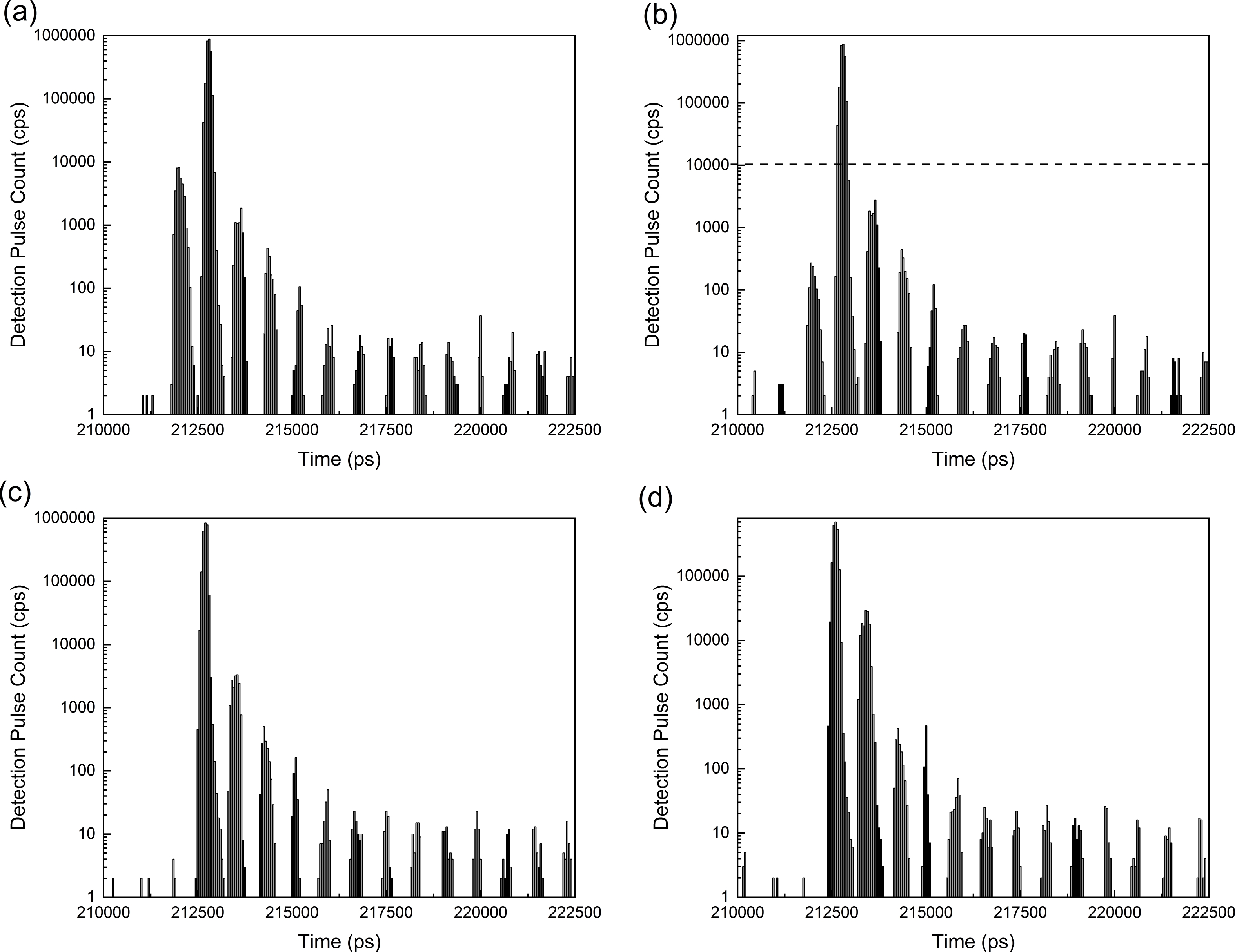
Quantum key distribution (QKD) achieves information-theoretic security based on quantum mechanics principles, where single-photon detectors (SPDs) serve as critical components. This study focuses on the sinusoidal gated SPDs widely used in high-speed QKD systems. We investigate the mechanisms underlying the rising-edge jitter in detection signals, identifying contributions from factors such as the temporal width of injected optical pulses, avalanche generation processes, avalanche signal extraction, and pulse discrimination. To address the issue of excessive jitter-induced bit errors, we propose a retiming scheme that utilizes coincidence signals synchronized with the sinusoidal gating signal. This approach effectively suppresses detection signal jitter and reduces the after-pulse probability of the detector. Experimental validation using a high-precision time-to-digital converter (TDC) demonstrates a significant reduction in the rising-edge jitter distribution after applying the suppression scheme. The proposed method features clear principles and straightforward engineering implementation, avoiding direct interference with the detector’s operational processes. The designed high-speed sinusoidal gated InGaAs/InP SPD operates at 1.25 GHz, achieving a remarkable reduction in after-pulse probability from 10.7% (without jitter suppression) to 0.72%, thereby enhancing the overall performance of QKD systems.

J. Semicond.
2025, 46(12): 122501 doi: 10.1088/1674-4926/25040026
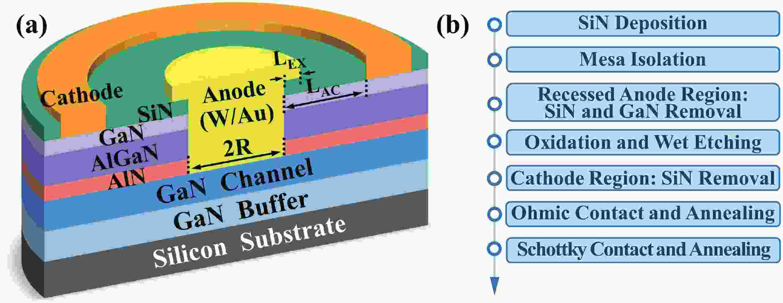
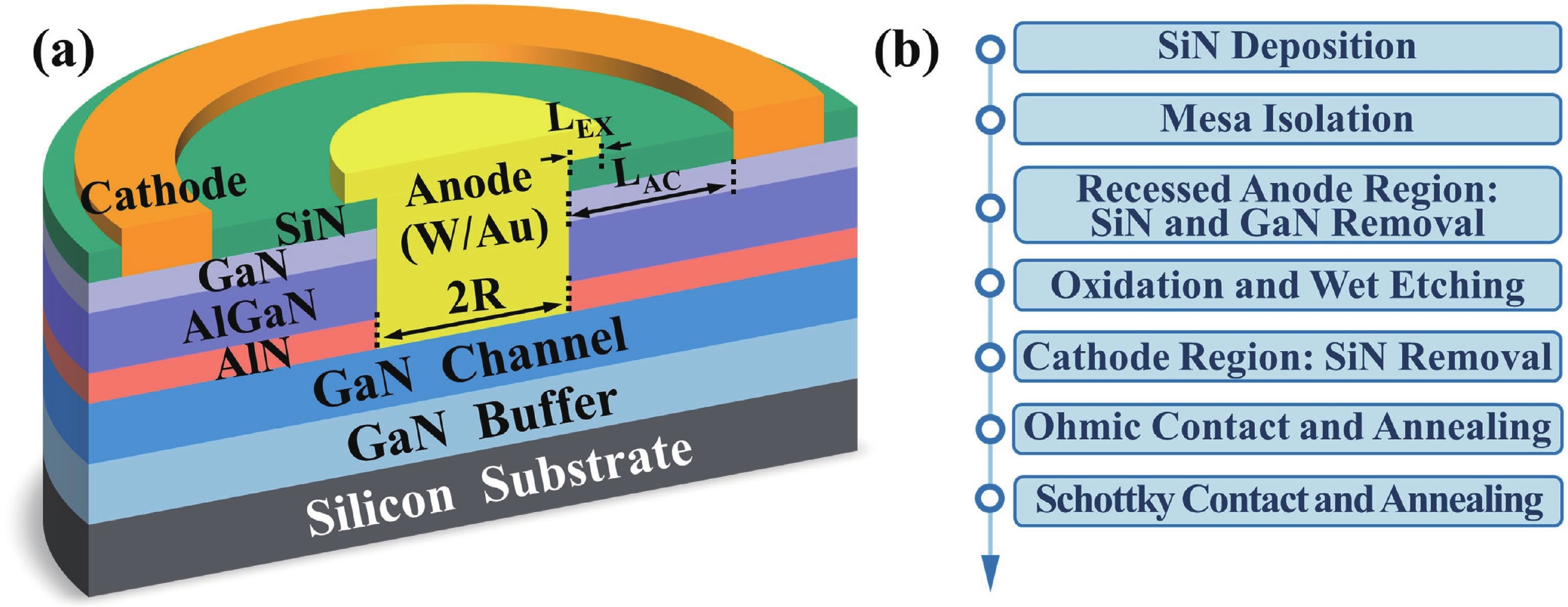
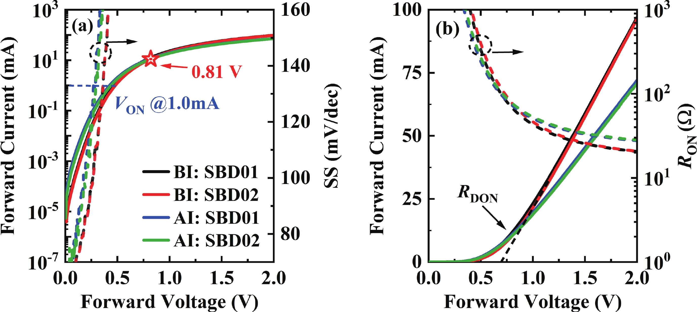
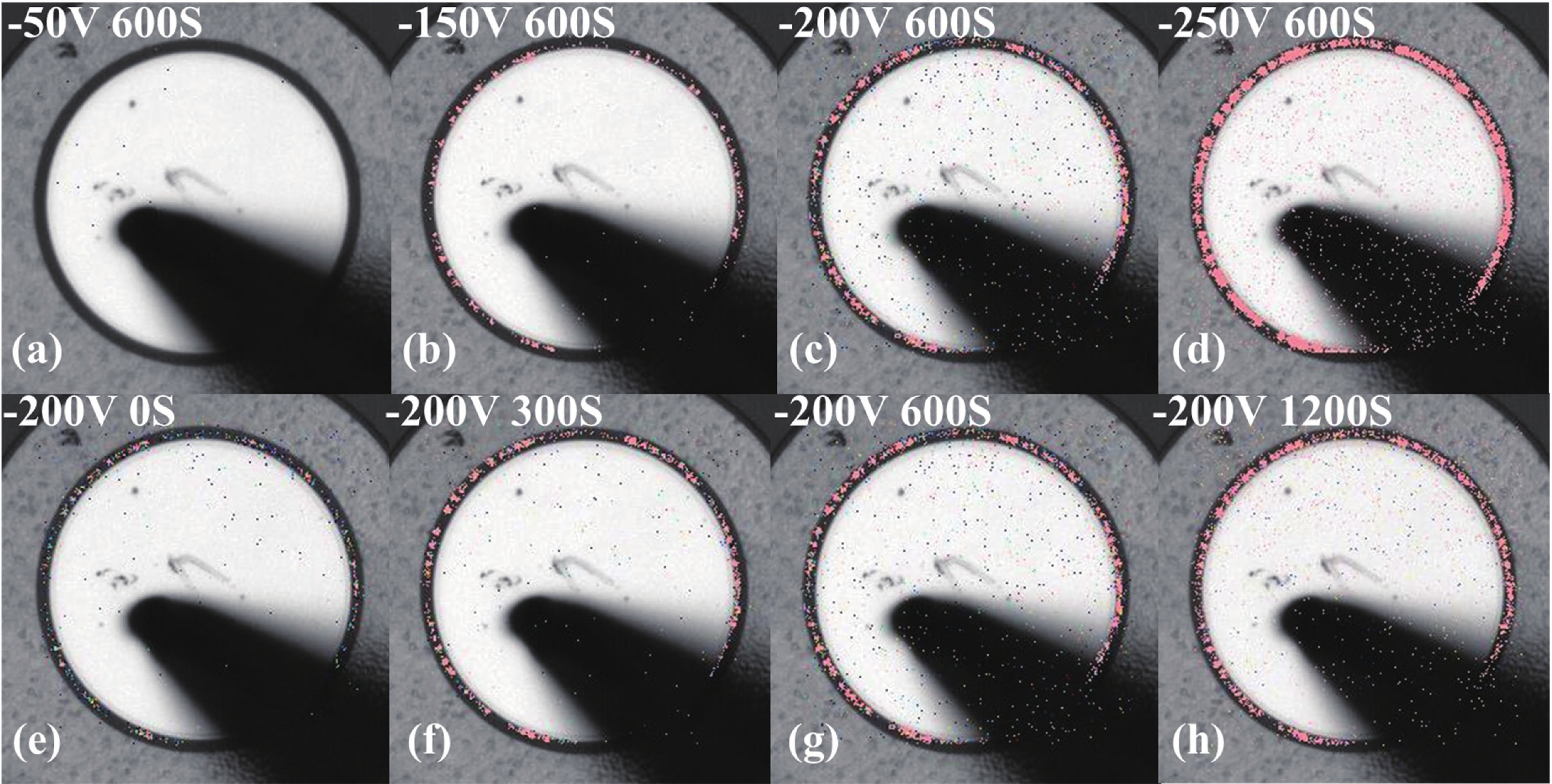
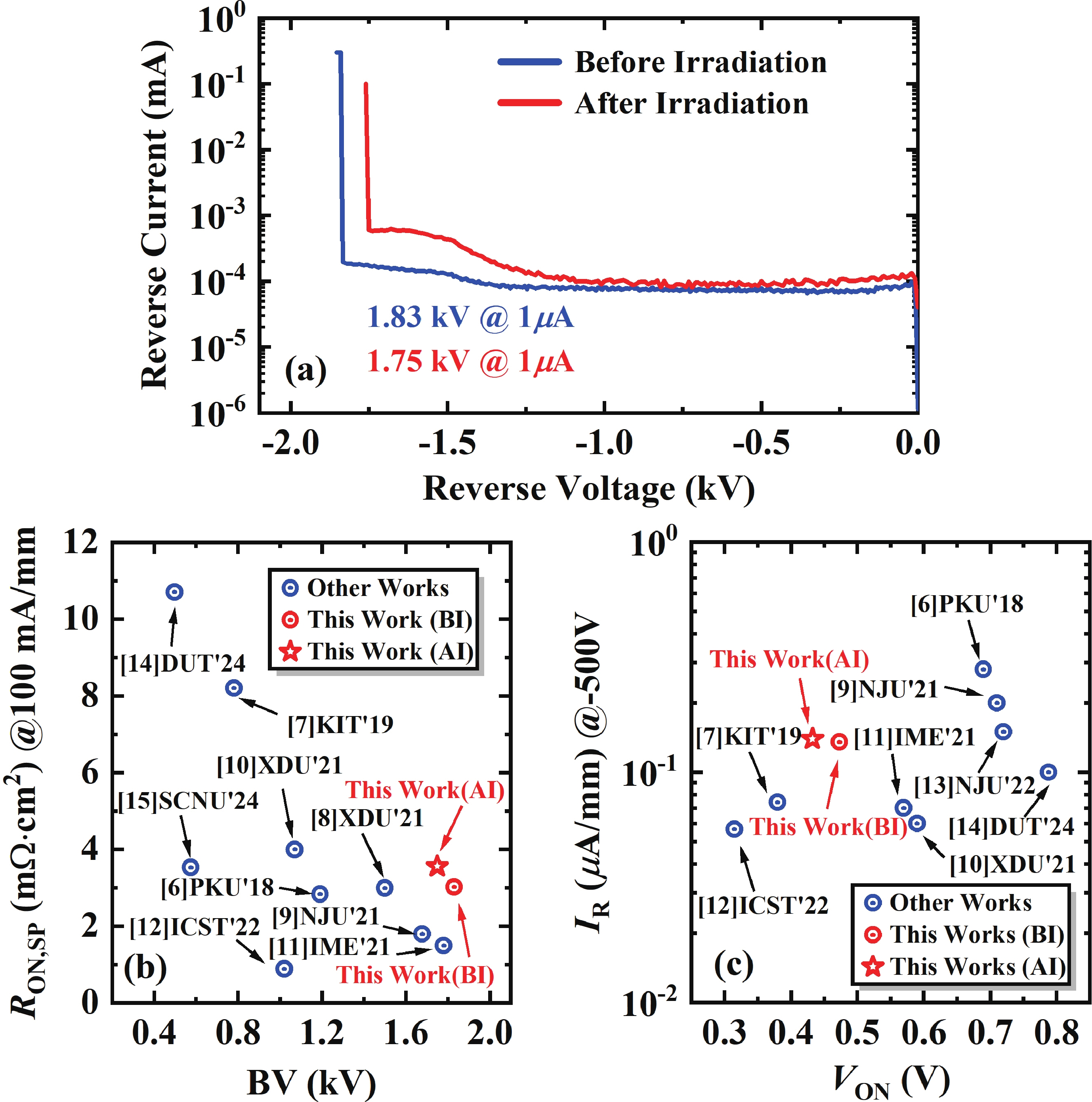
In this letter, we demonstrate the effect of γ irradiation on the lateral AlGaN/GaN Schottky barrier diodes (SBDs) with self-terminated recessed anode structure and low work-function metal tungsten (W) as anode. For a comprehensive evaluation of the radiation-resistance performance of the device, the total dose of γ irradiation is up to 100 kGy with irradiation time of 20 h. Attributed to the barrier lowering effect of the W/GaN interface induced by γ irradiation observed in the experiment, the extracted turn-on voltage (VON) defined at anode forward current of 1 mA decreases from 0.47 to 0.43 V. Meanwhile, benefiting from the reinforced Schottky interface treated by post-anode-annealing, a high breakdown voltage (BV) of 1.75 kV is obtained for the γ-irradiated AlGaN/GaN SBD, which shows the promising application for the deep-space radiation environment and promotes the development of radiation-resistance research for GaN SBDs.
J. Semicond.
2025, 46(12): 122601 doi: 10.1088/1674-4926/25020031

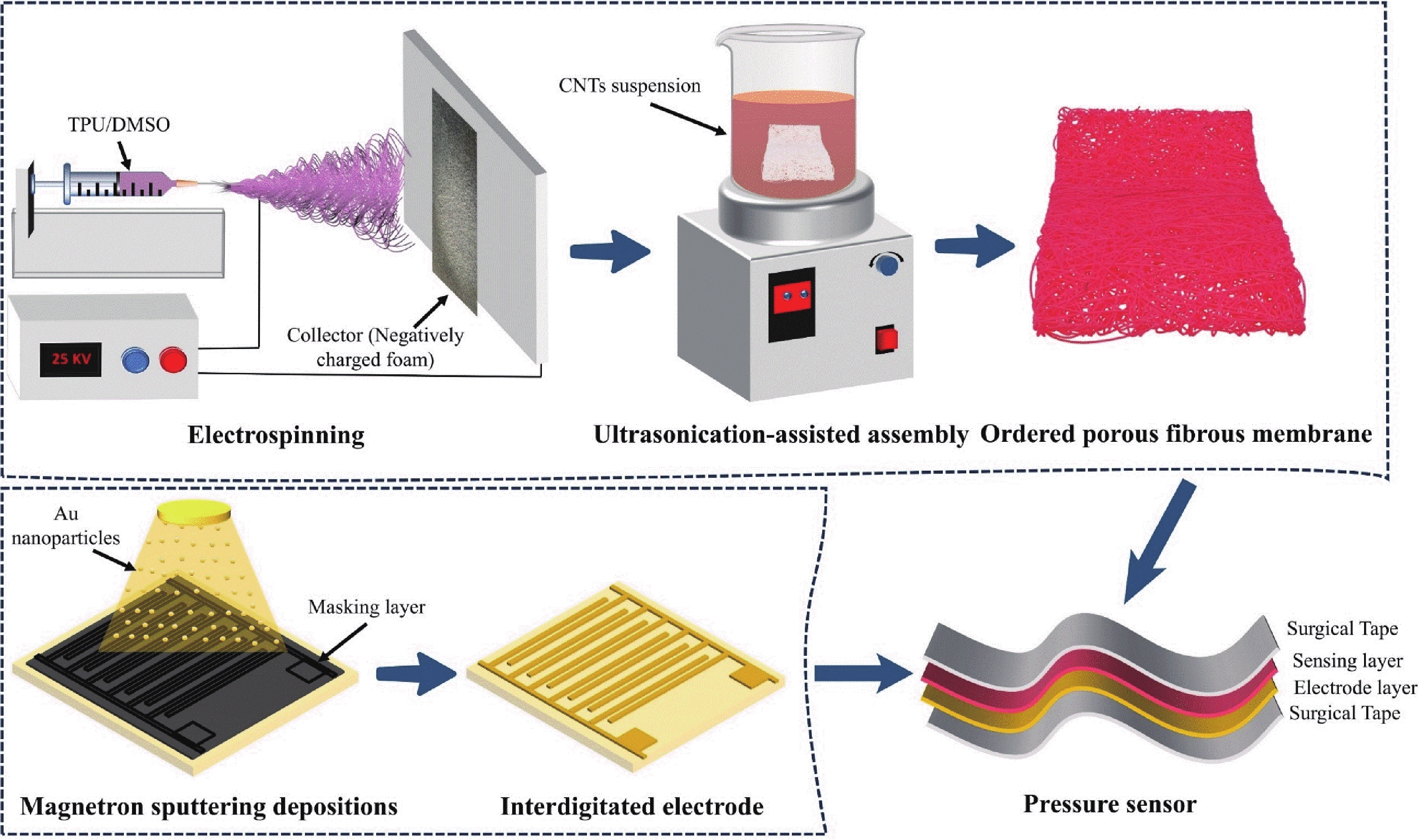
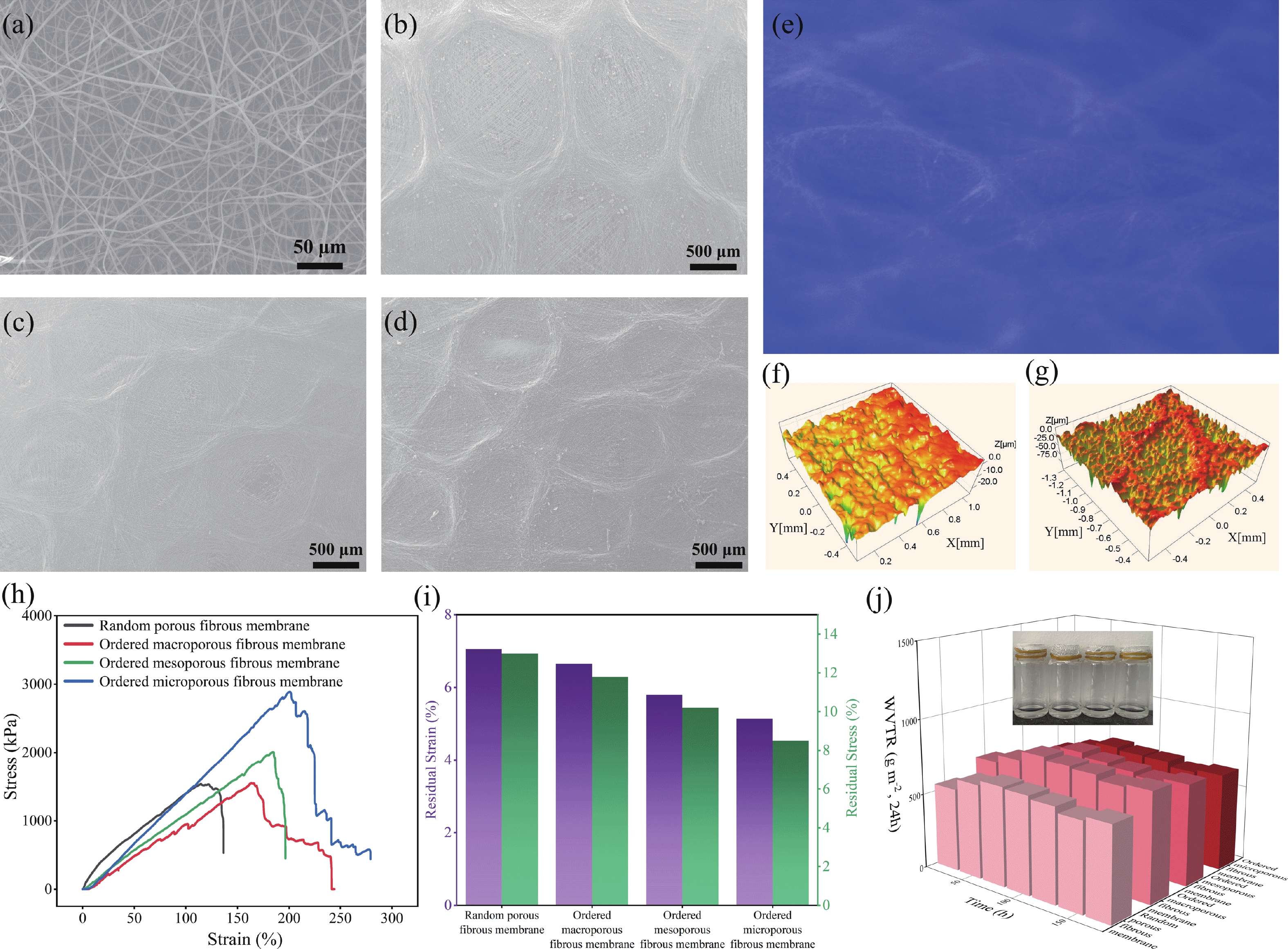
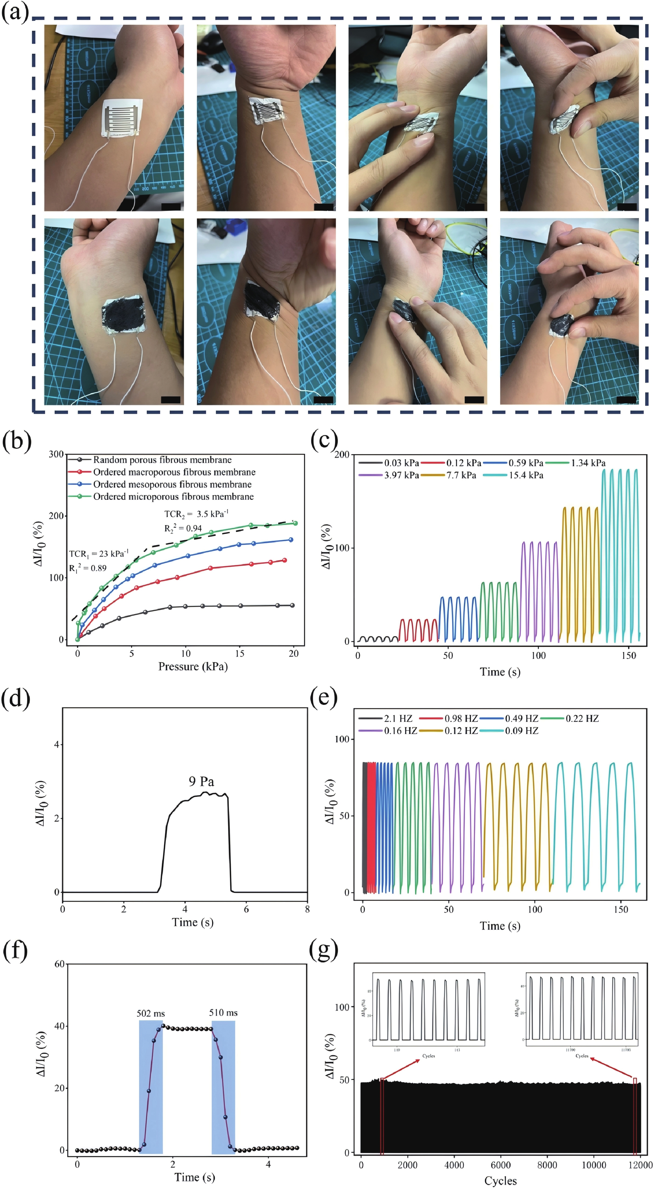
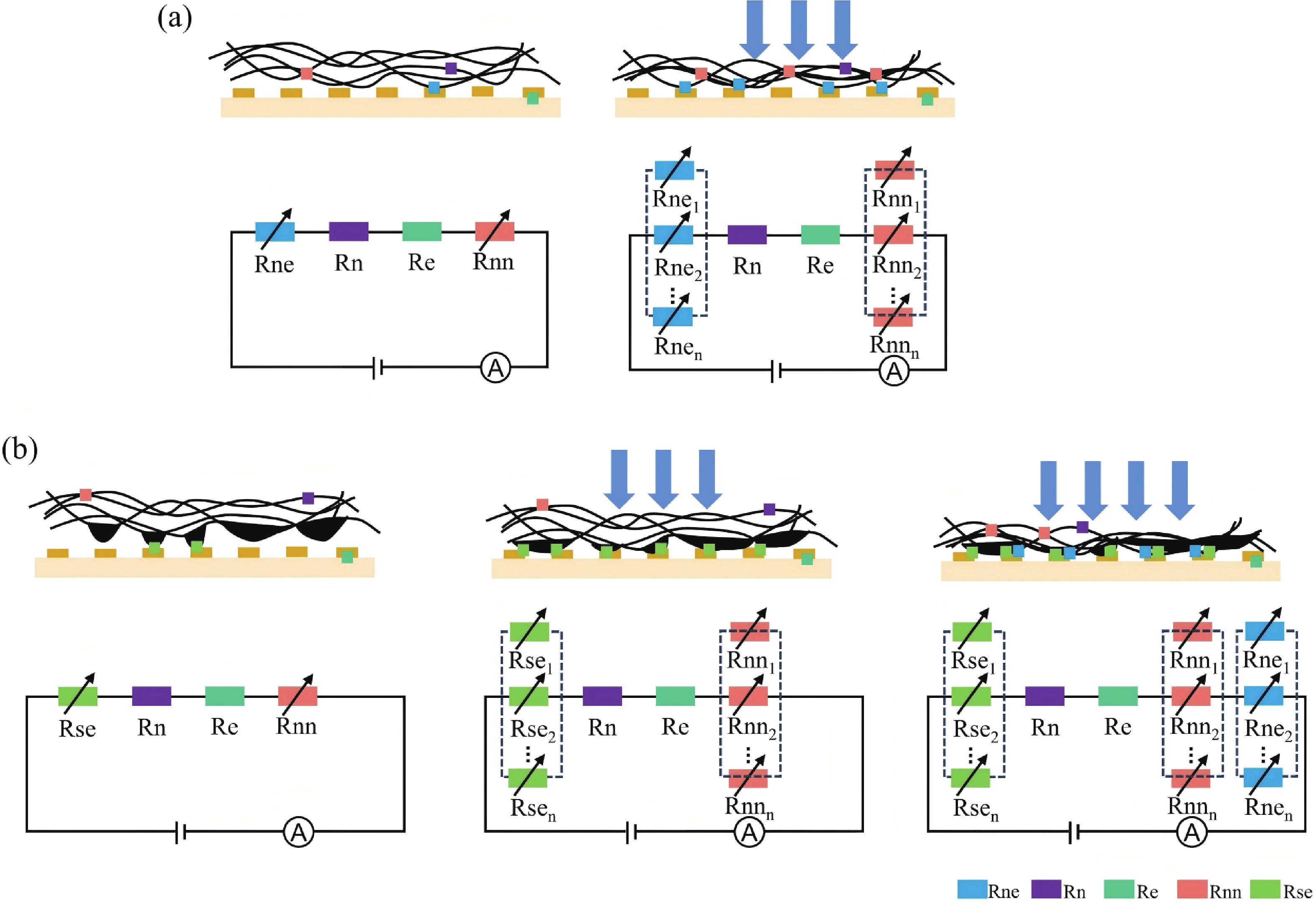
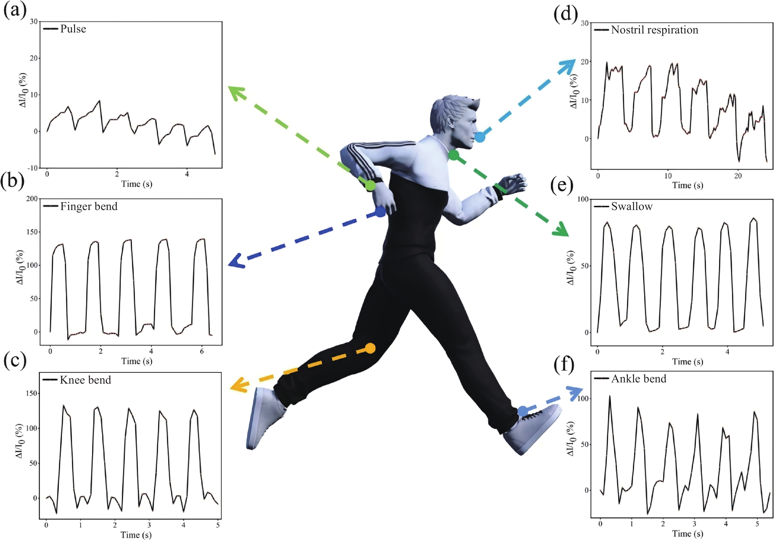
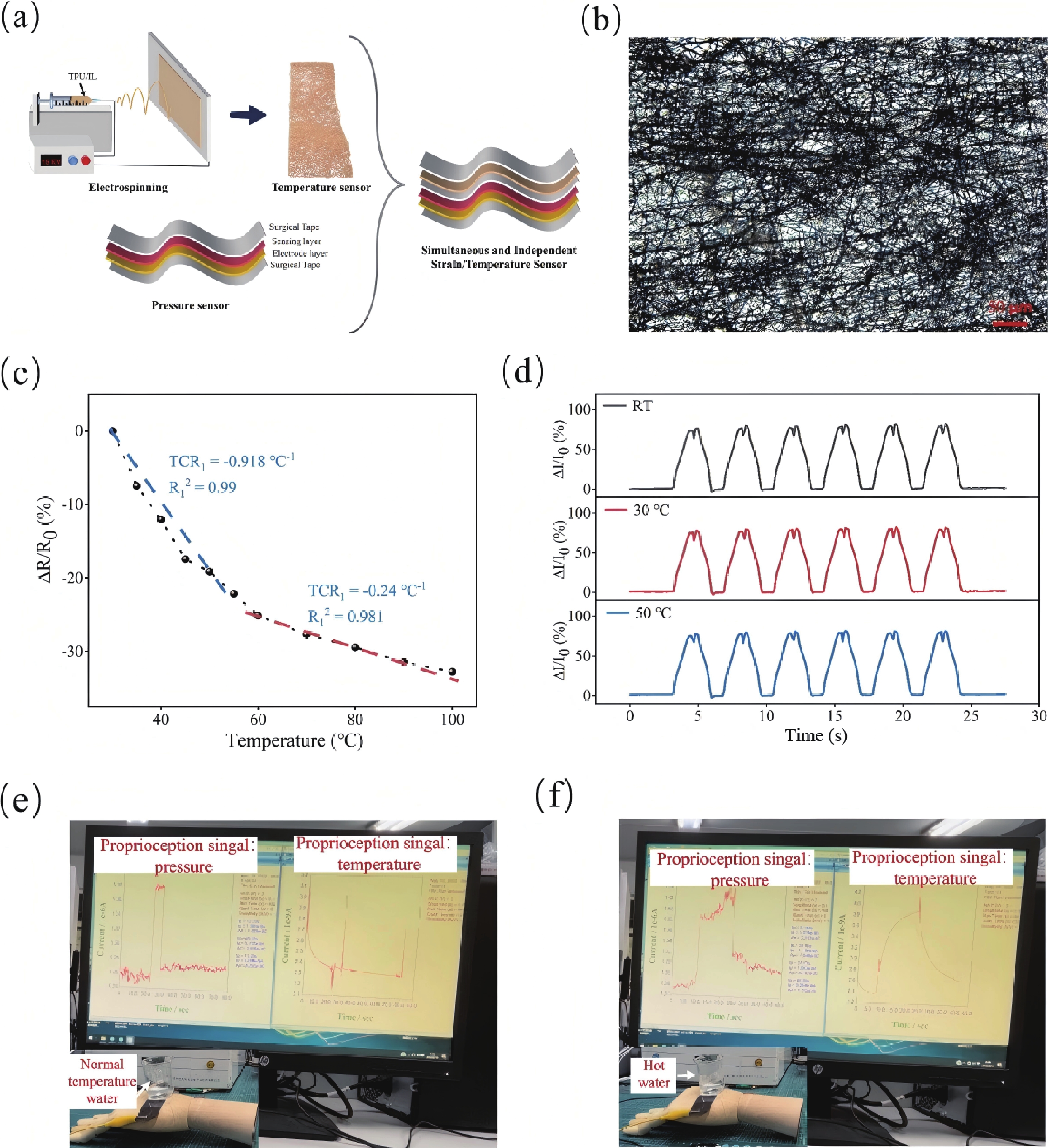
The random nanofiber distribution in traditional electrospun membranes restricts the pressure sensing sensitivity and measurement range of electronic skin. Moreover, current multimodal sensing suffers from issues like overlapping signal outputs and slow response. Herein, a novel electrospinning method is proposed to prepare double-coupled microstructured nanofibrous membranes. Through the effect of high voltage electrostatic field in the electrospinning, the positively charged nanofibers are preferentially attached to the negatively charged foam surface, forming the ordered two-dimensional honeycomb porous nanofibrous membrane with three-dimensional spinous microstructure. Compared with the conventional random porous nanofibrous membrane, the bionic two-dimensional honeycomb and three-dimensional spinous dual-coupled microstructures in the ordered porous nanofibrous membrane endows the electronic skin with significantly improved mechanical properties (maximum tensile strain increased by 77% and fatigue resistance increased by 35%), air permeability (water vapor transmission rate increased by 16%) and sensing properties (pressure sensitivity increased by 276% and detection range increased by 137%). Furthermore, the electronic skin was constructed by means of a conformal composite ionic liquid functionalized nanofibrous membrane, and the real-time and interference-free dual-signal monitoring of pressure and temperature (maximum temperature coefficient of resistance: −0.918 °C−1) was realized.
J. Semicond.
2025, 46(12): 122701 doi: 10.1088/1674-4926/25030041
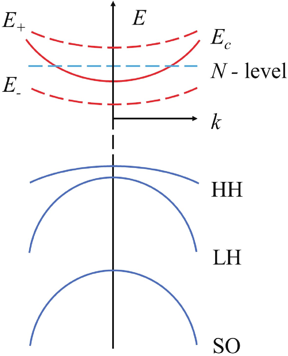
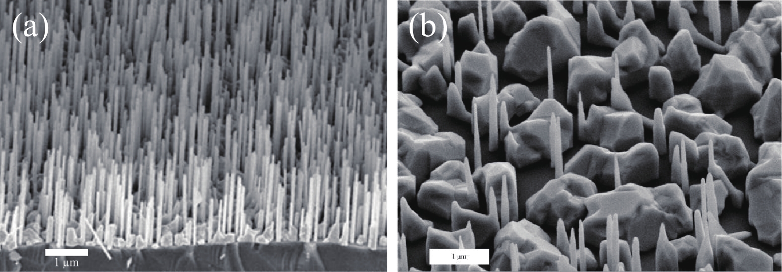
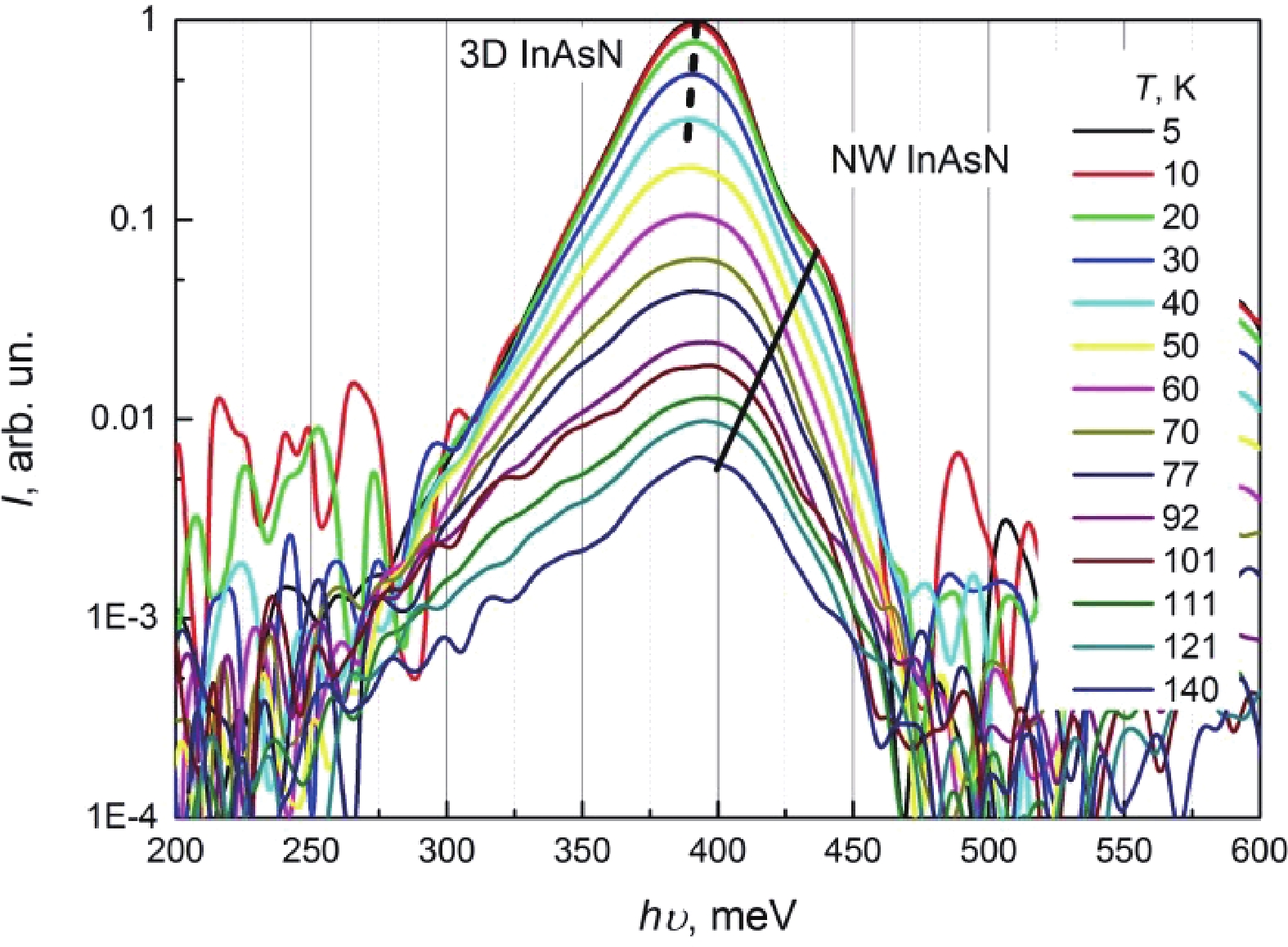
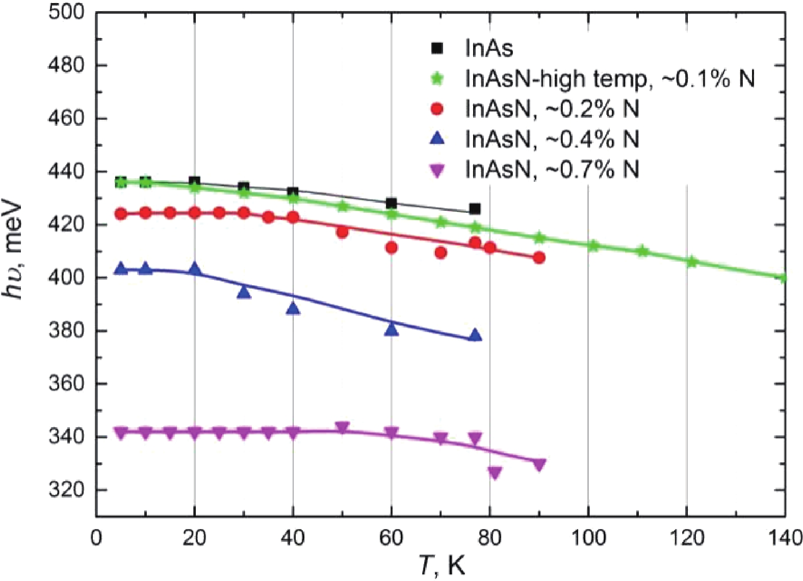
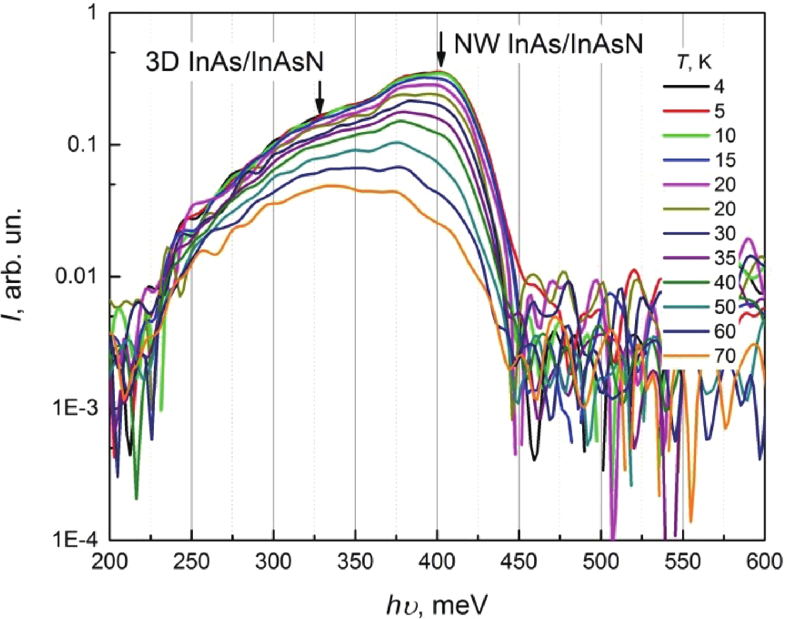
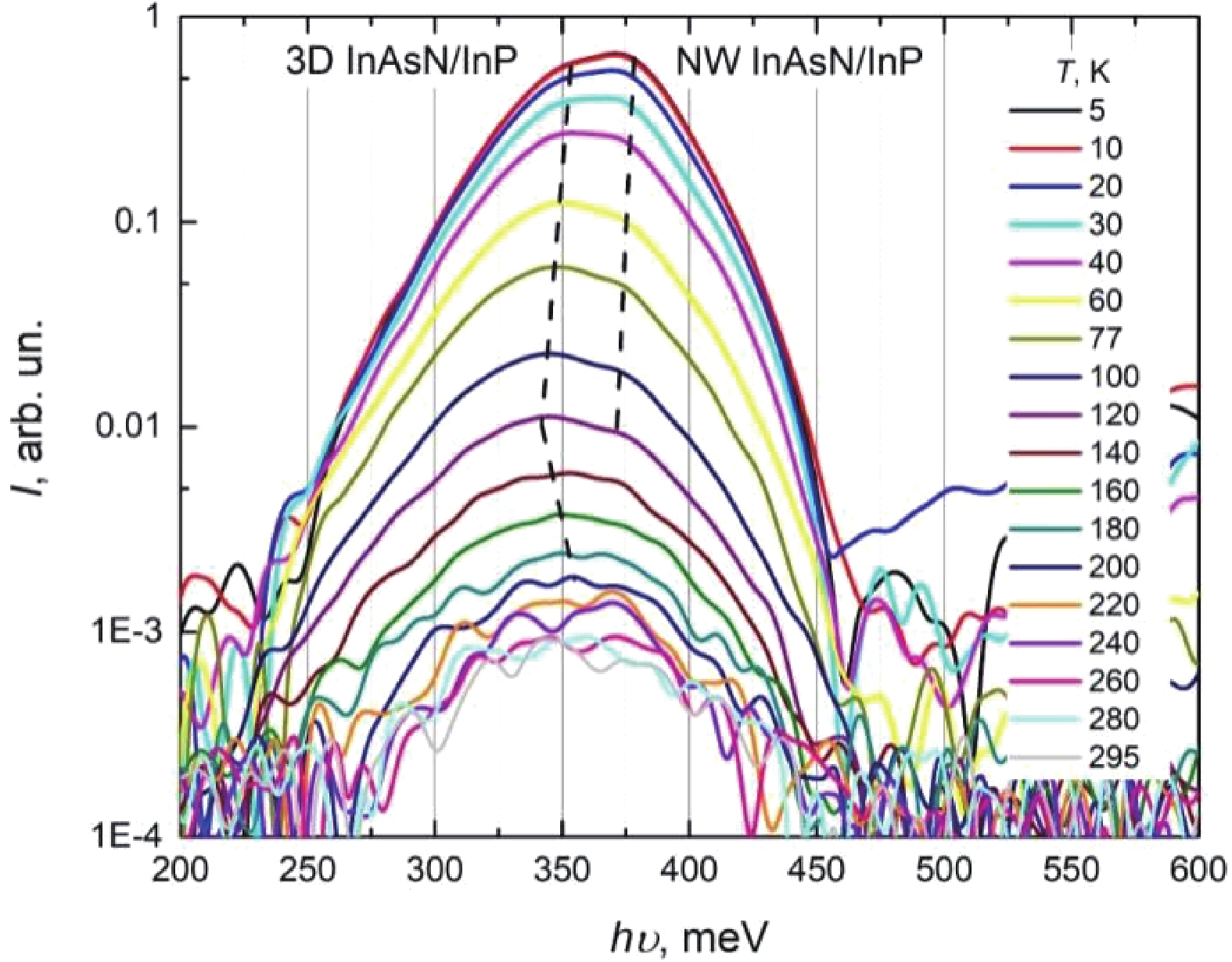
InAsN nanowires on InAs stems were obtained using plasma-assisted molecular beam epitaxy on a SiOx/Si (111) substrate. Also, heterostructured InAs/InAsN and InAsN/InP nanowires were grown in the core/shell geometry. In the low-temperature photoluminescence spectra of the grown structures, spectral features are observed that correspond to the polytypic structure of nanowires with a predominance of the wurtzite phase and parasitic islands of the sphalerite phase. It was shown that the interband photoluminescence spectral features of InAsN nanowires experience a red shift relative to the pristine InAs nanowires. The incorporation of nitrogen reduces the bandgap by splitting the conduction band into two subbands. The position of the spectral features in the photoluminescence spectra confirms the formation of a nitride solid solution with a polytypic hexagonal structure, having a concentration of nitrogen atoms of up to 0.7%. Additional passivation of the nanowire surface with InP leads to a decrease in the intensity of nonradiative recombination and an improvement in the photoluminescent response of the nanowires, which makes it possible to detect photoluminescence emission at room temperature. Thus, by changing the composition and morphology of nanowires, it is possible to control their electronic structure, which allows varying the operating range of detectors and mid-IR radiation sources based on them.