Issue Browser
Volume 47, Issue 1,
Jan 2026
Column
J. Semicond.
2026, 47(1): 011101 doi: 10.1088/1674-4926/24120040

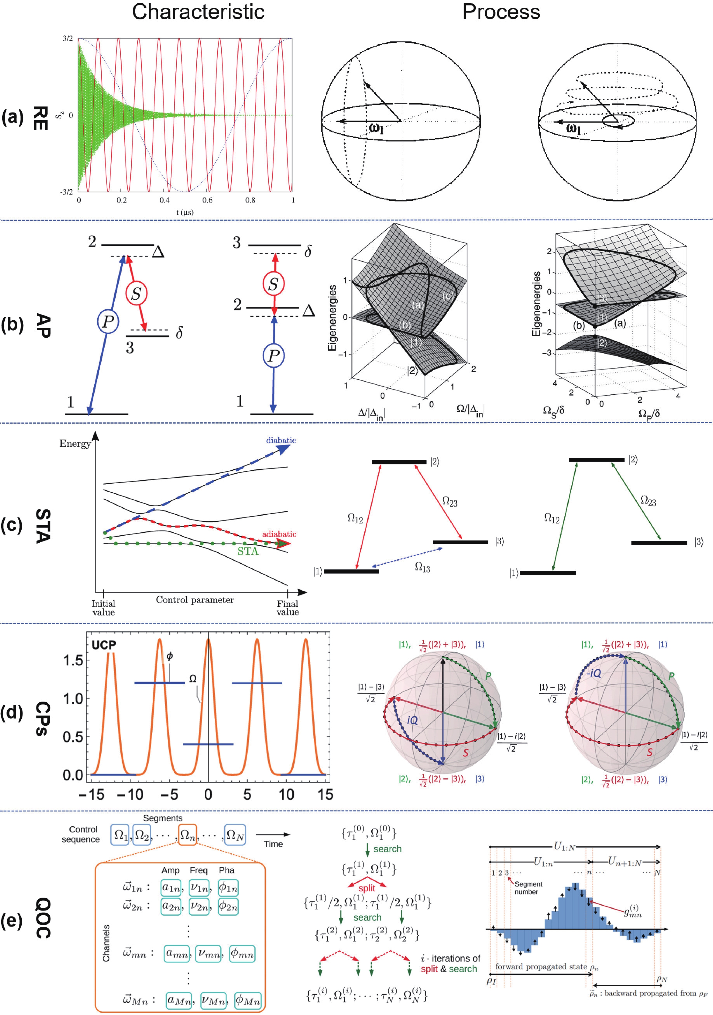
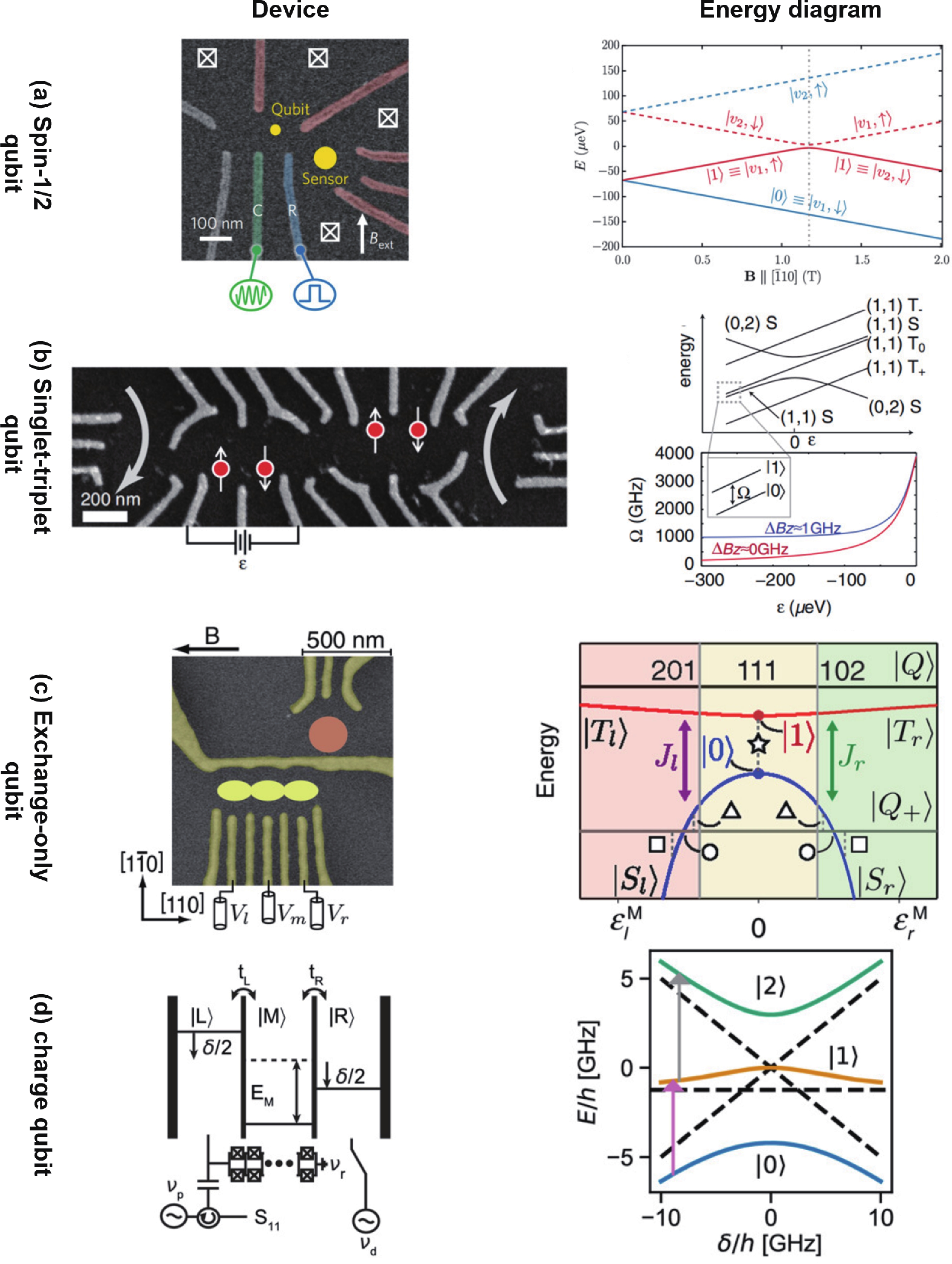
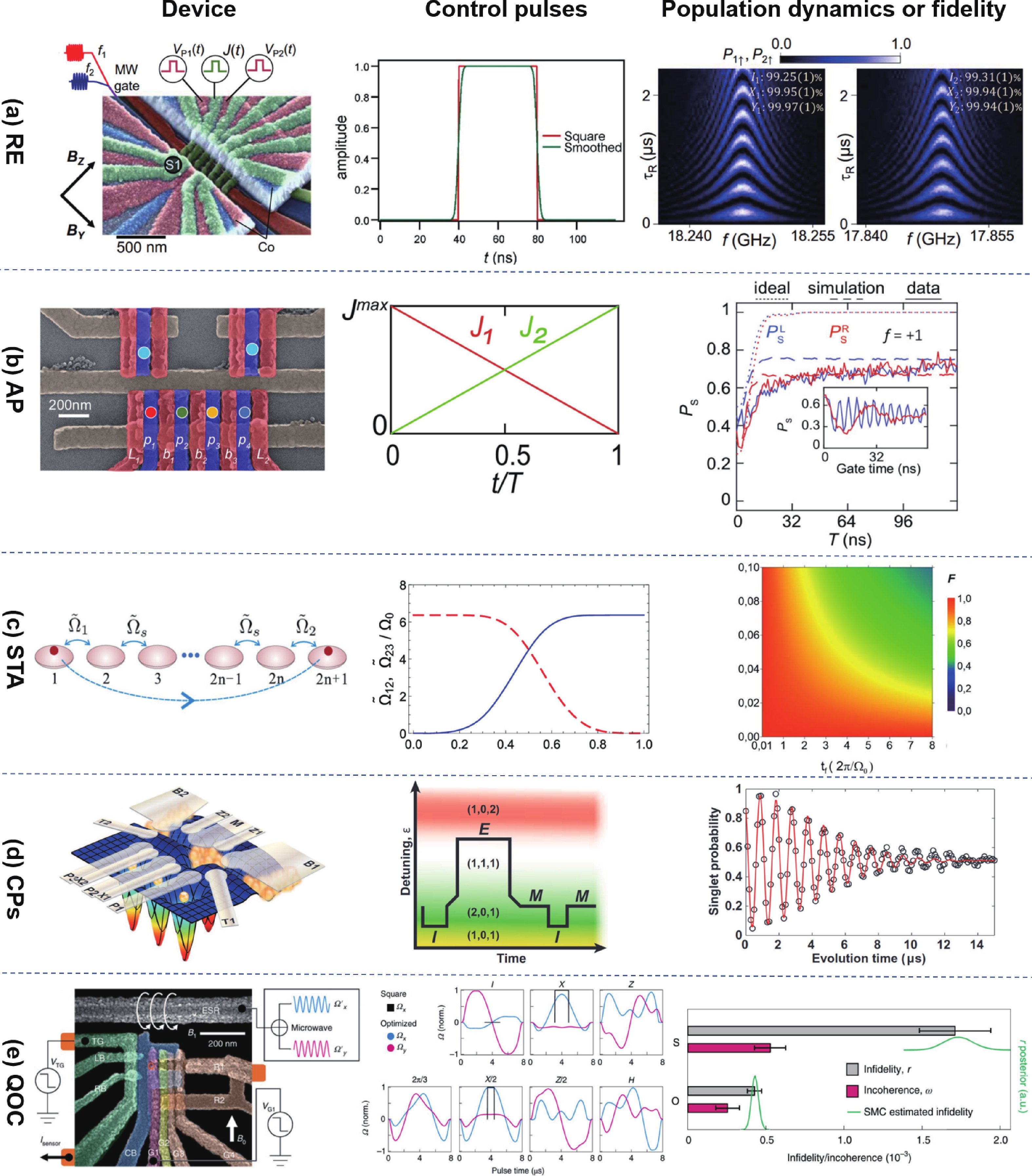
Quantum control allows a wide range of quantum operations employed in molecular physics, nuclear magnetic resonance and quantum information processing. Thanks to the existing microelectronics industry, semiconducting qubits, where quantum information is encoded in spin or charge degree freedom of electrons or nuclei in semiconductor quantum dots, constitute a highly competitive candidate for scalable solid-state quantum technologies. In quantum information processing, advanced control techniques are needed to realize quantum manipulations with both high precision and noise resilience. In this review, we first introduce the basics of various widely-used control methods, including resonant excitation, adabatic passage, shortcuts to adiabaticity, composite pulses, and quantum optimal control. Then we review the practical aspects in applying these methods to realize accurate and robust quantum gates for single semiconductor qubits, such as Loss–DiVincenzo spin qubit, spinglet-triplet qubit, exchange-only qubit and charge qubit.
J. Semicond.
2026, 47(1): 012301 doi: 10.1088/1674-4926/25040027

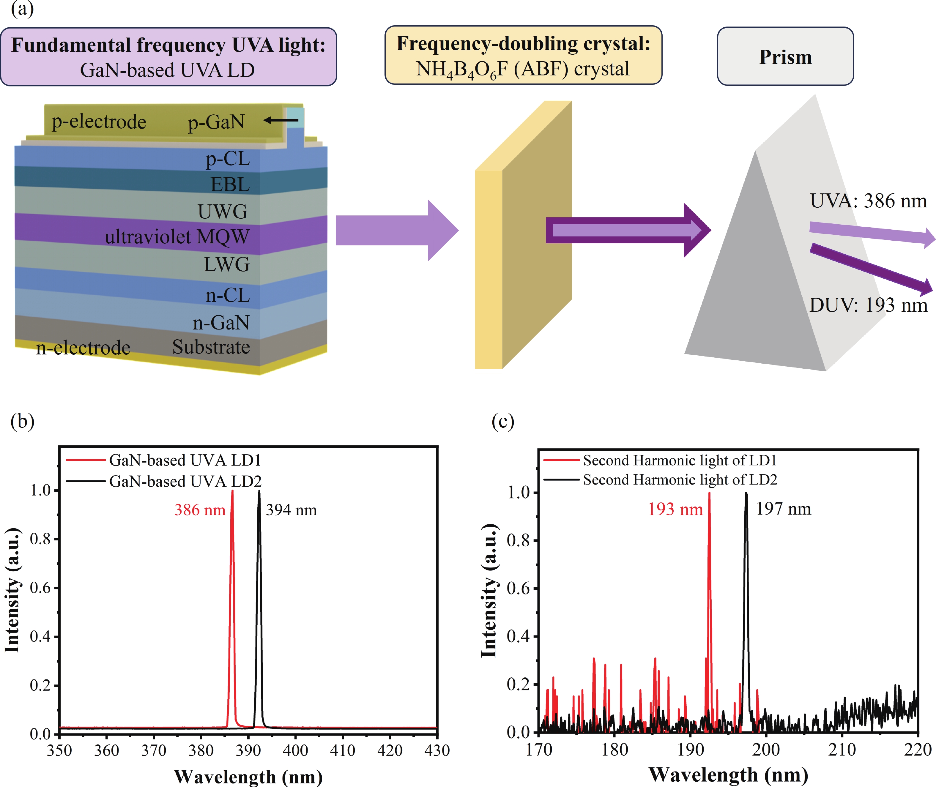
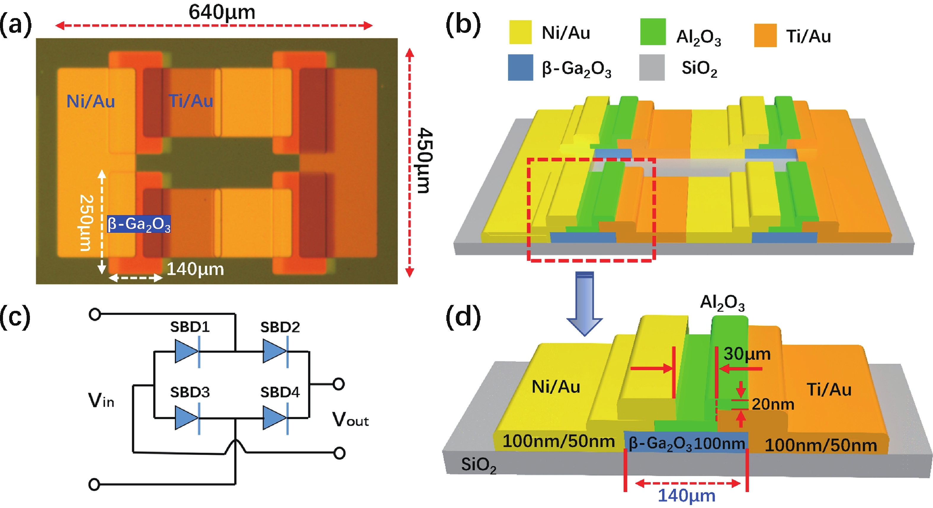
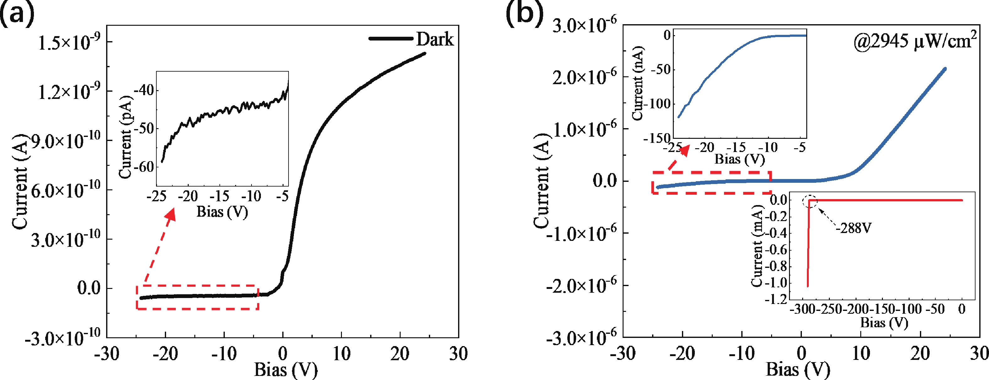
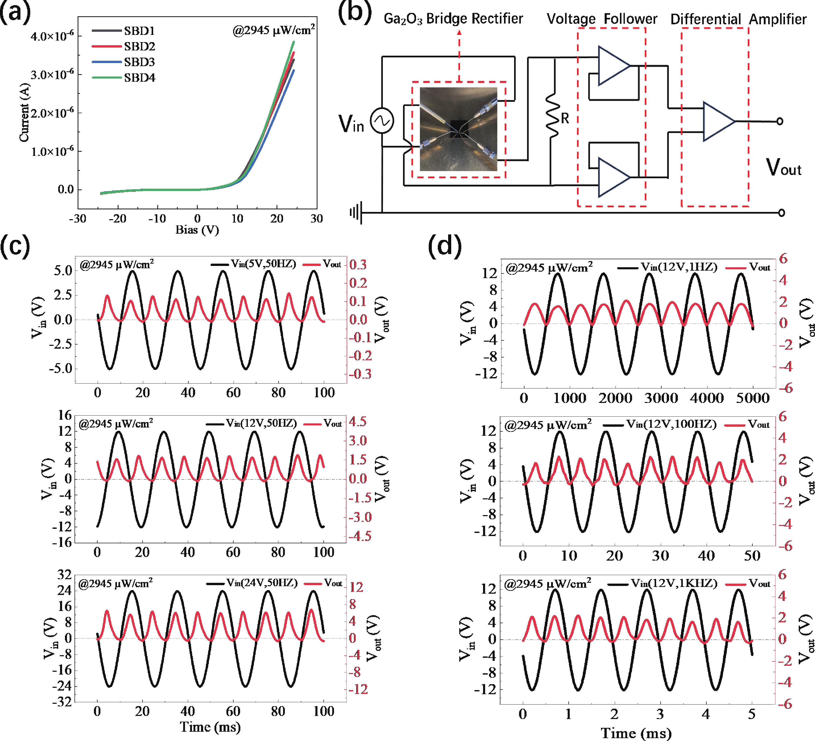
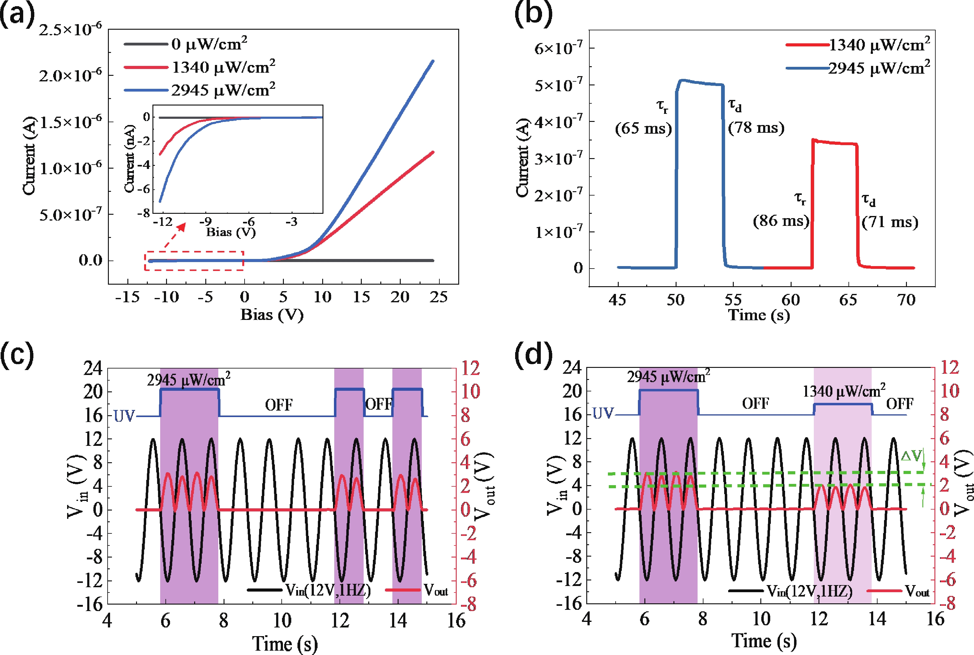
A monolithic integrated full-wave bridge rectifier consisted of horizontal Schottky-barrier diodes (SBD) is prepared based on 100 nm ultra-thin β-Ga2O3 and demonstrated the solar-blind UV (SUV) light-modulated characteristics. Under SUV light illumination, the rectifier has the excellent full-wave rectification characteristics for the AC input signals of 5, 12, and 24 V with different frequencies. Further, experimental results confirmed the feasibility of continuously tuning the rectified output through SUV light-encoding. This work provides valuable insights for the development of optically programmable Ga2O3 AC-DC converters.
J. Semicond.
2026, 47(1): 012302 doi: 10.1088/1674-4926/25030039
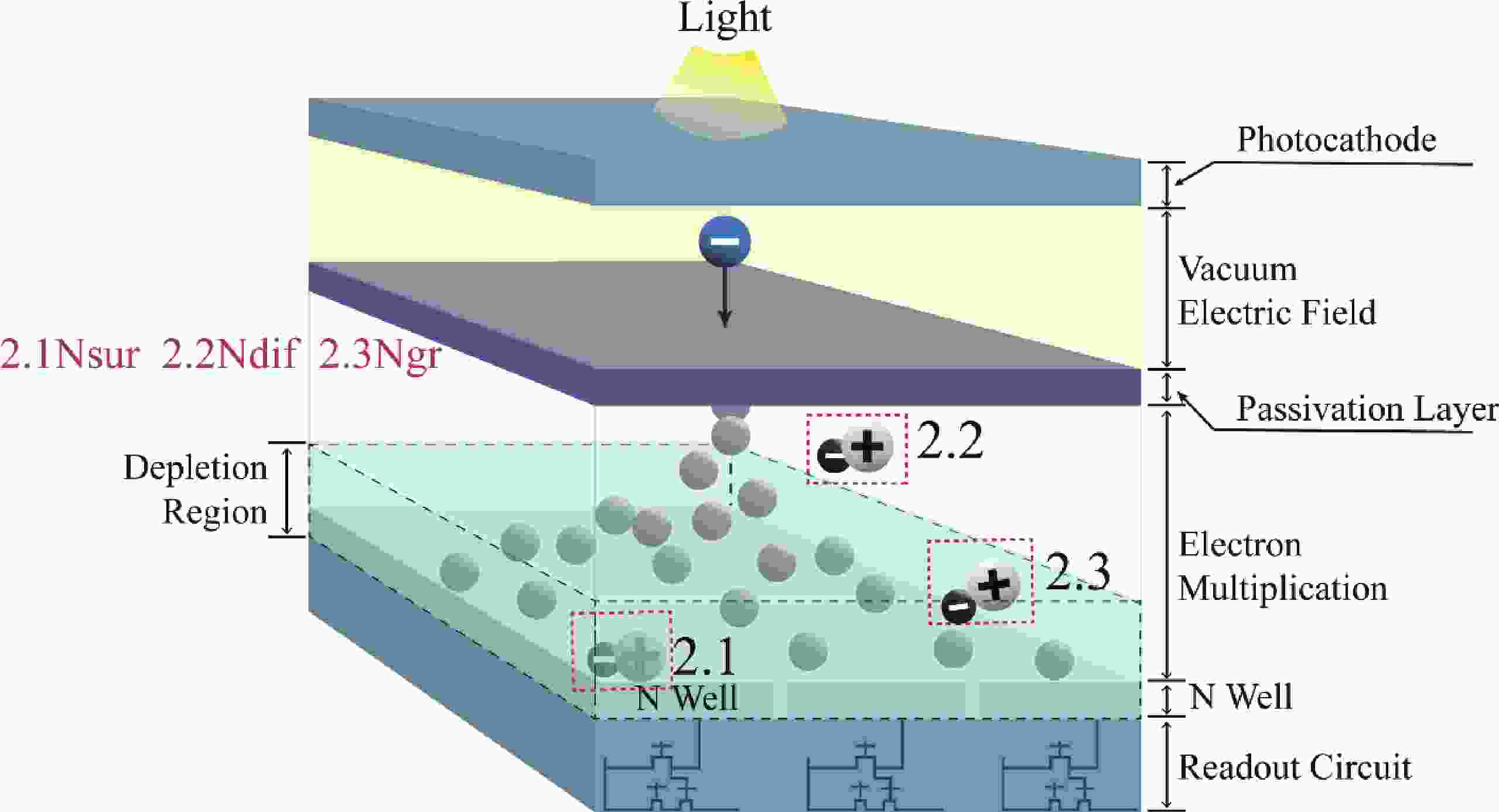
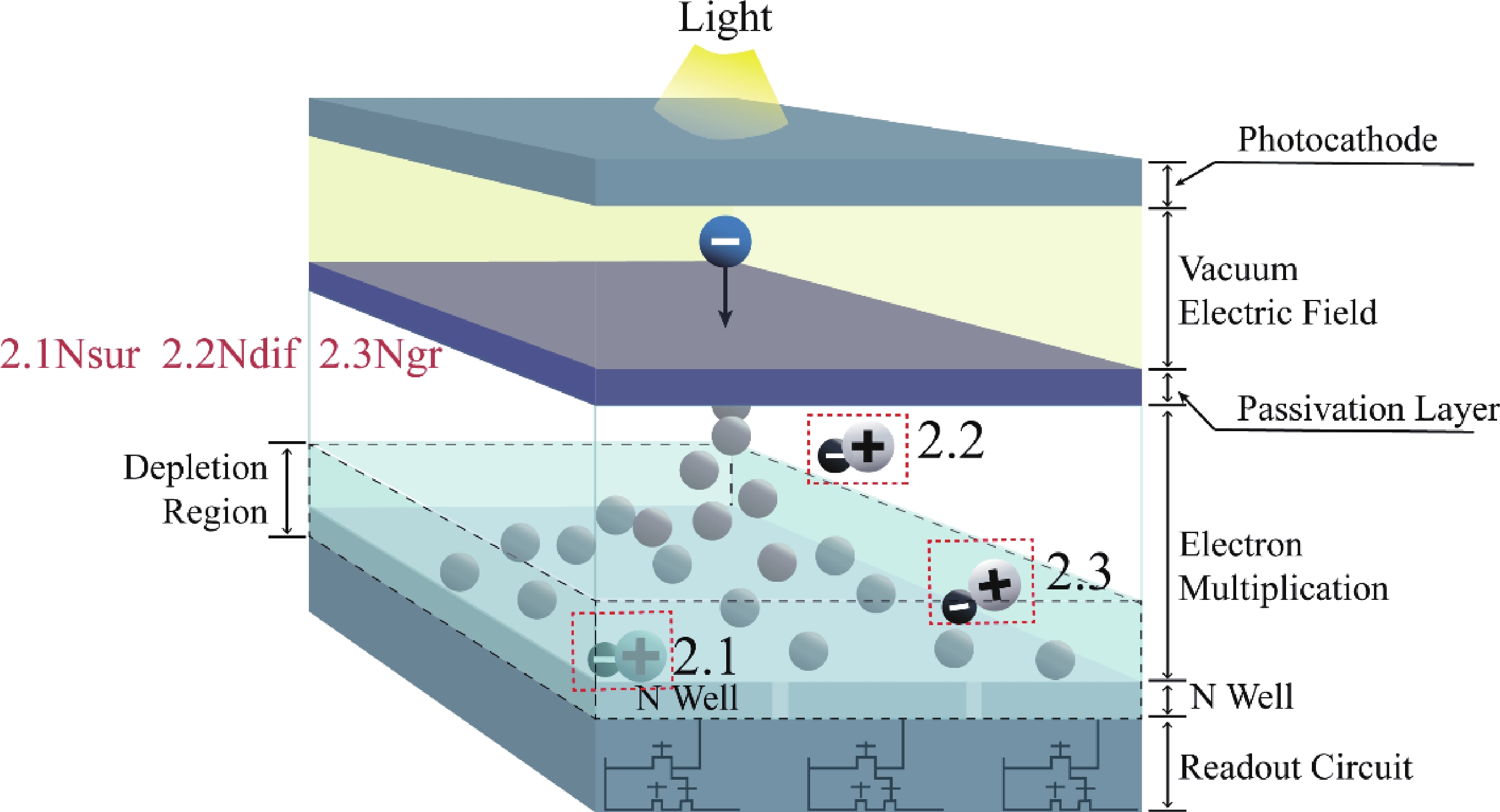
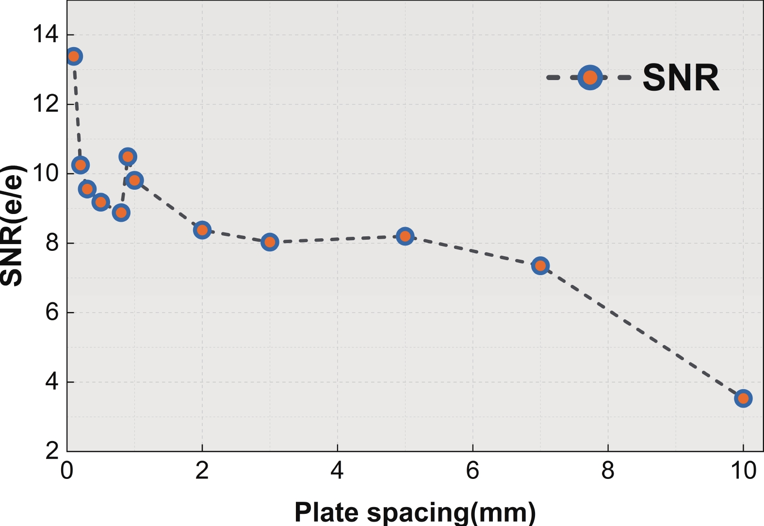
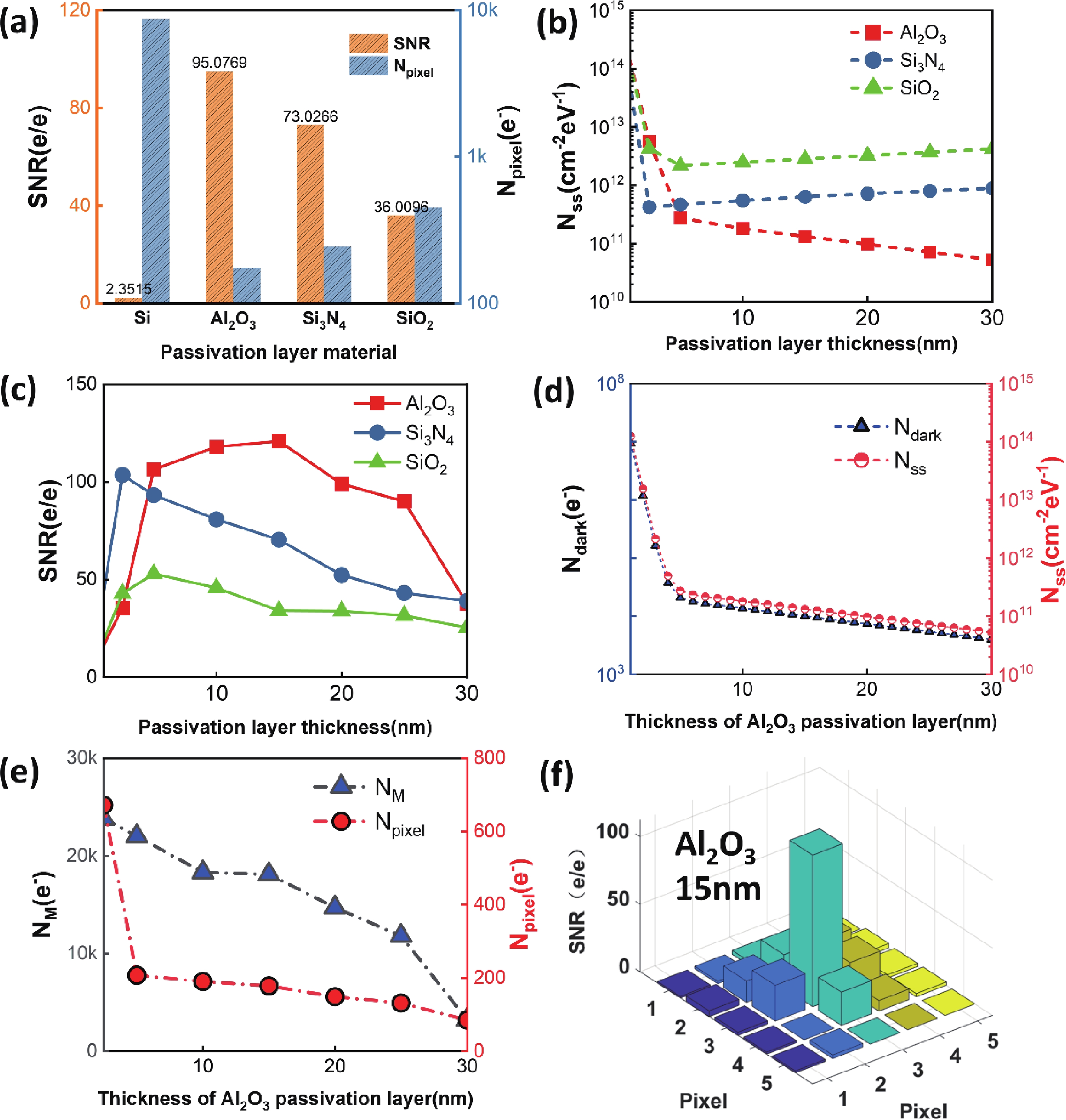
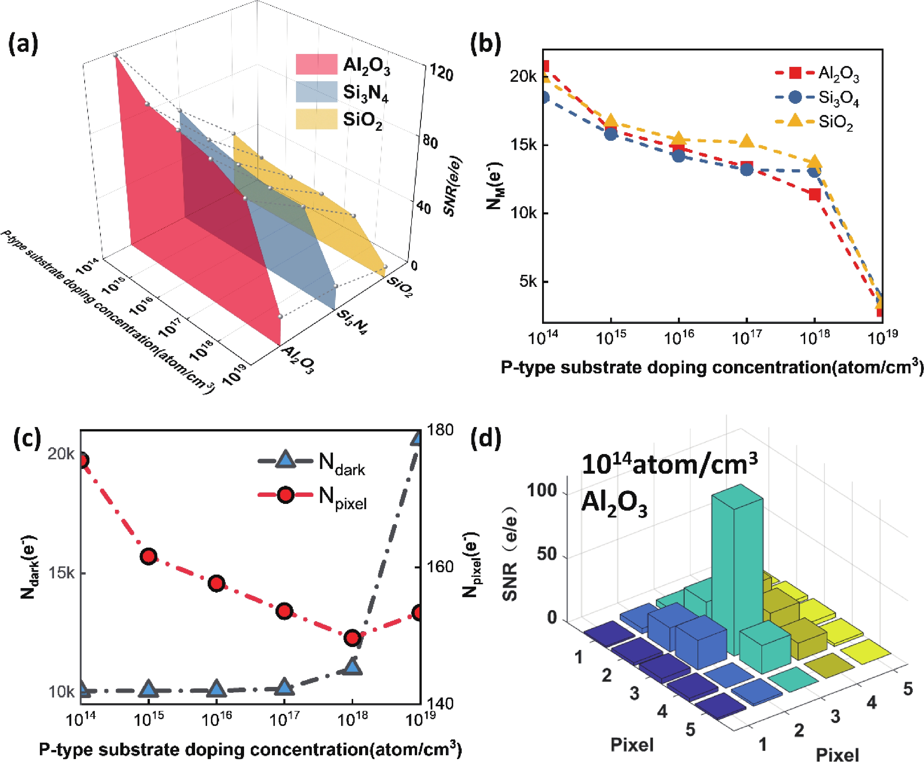
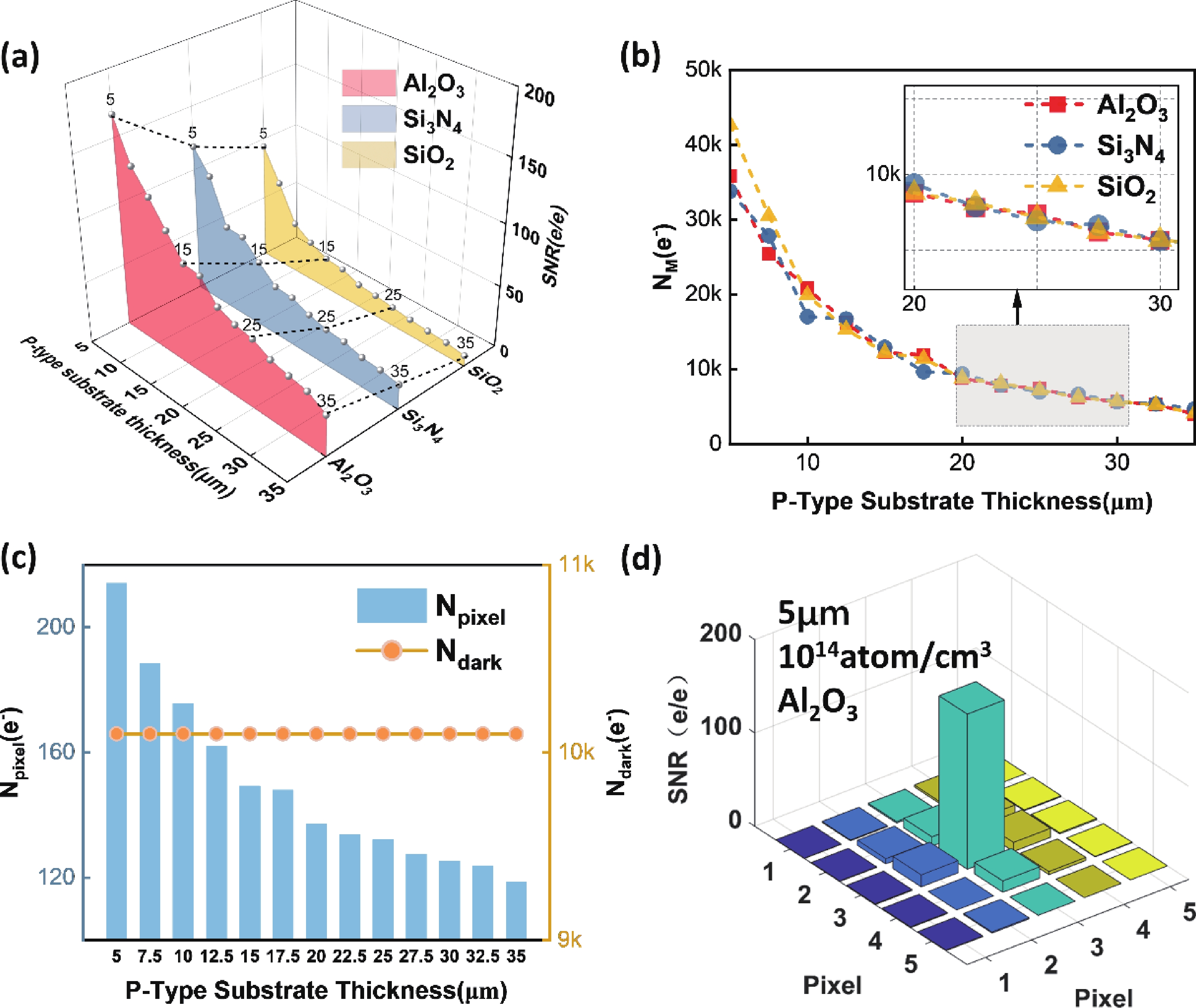
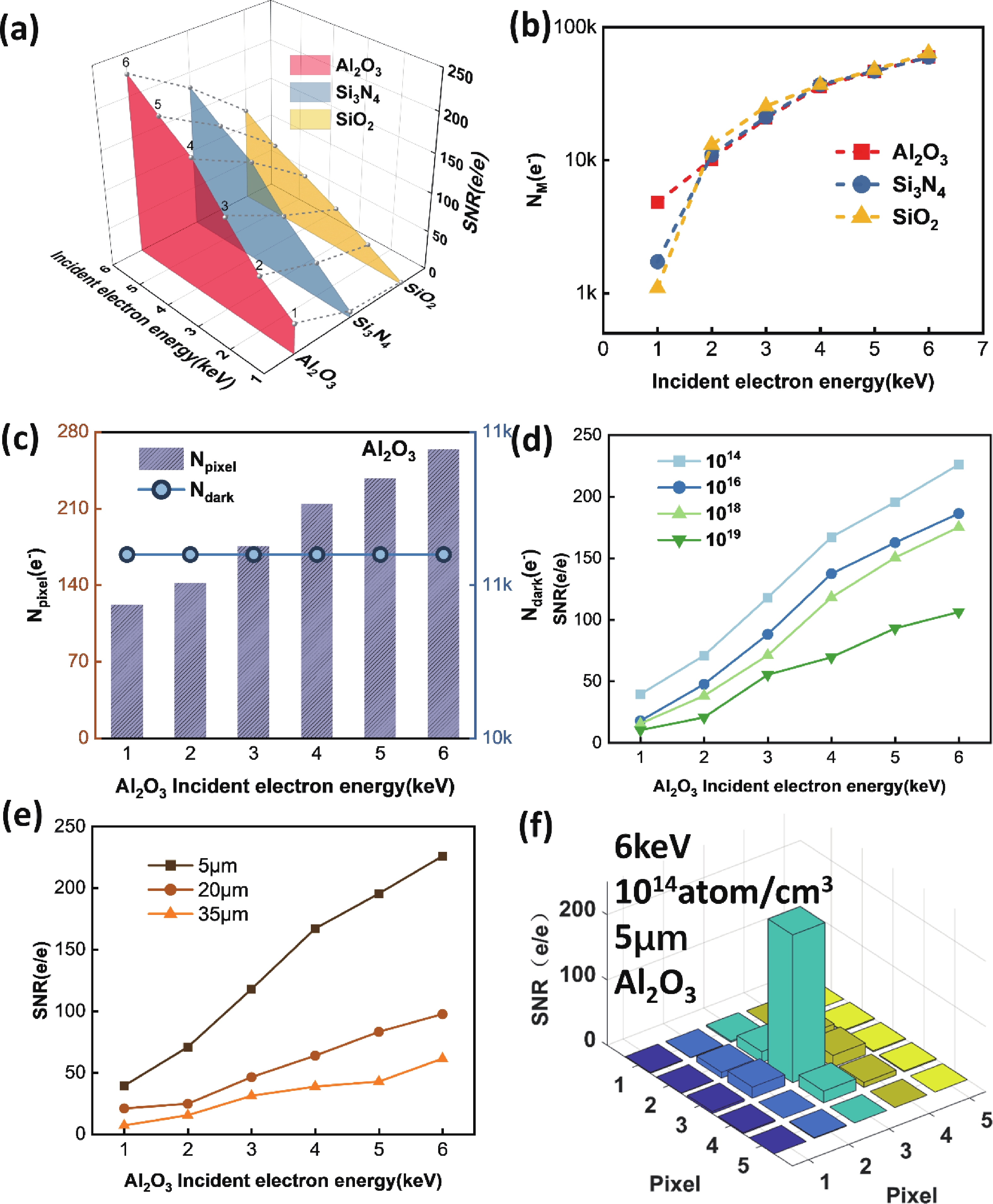
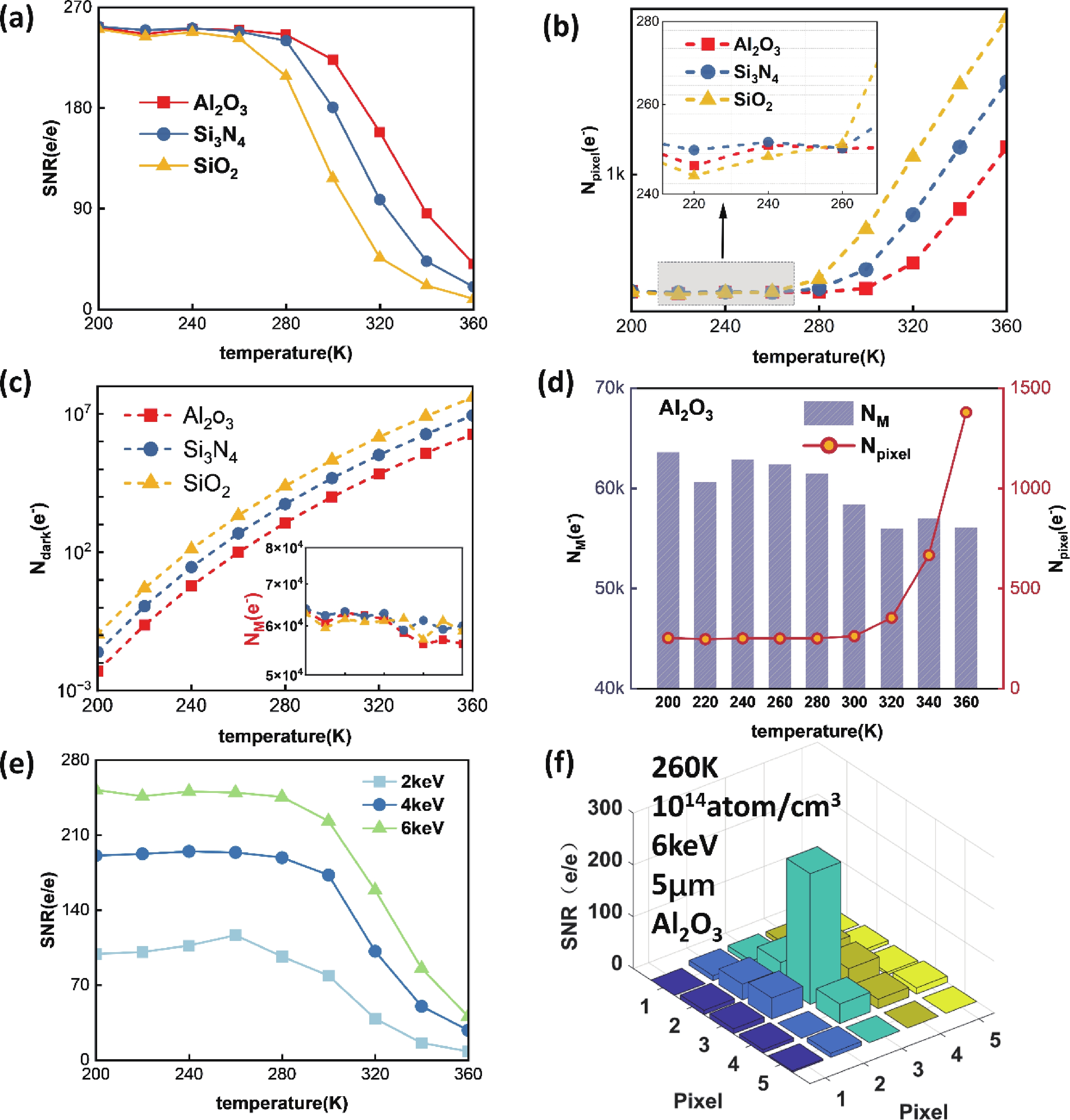
In this study, with the aim of achieving a high signal-to-noise ratio (SNR) in an electron-bombarded complementary metal−oxide−semiconductor (EBCMOS) imaging chip, we analyzed the sources of noise using principles from low-light-level imaging and semiconductor theory, and established a physical computational model that relates the electron-multiplication layer to the noise characteristics of an EBCMOS chip in a uniformly doped structure with a P-type substrate. We conducted theoretical calculations to analyze the effects on noise characteristics of the passivation layer material and thickness, P-substrate doping concentration, P-substrate thickness, incident electron energy, and substrate temperature. By comparing the characteristics of pixel noise, dark current, multiplication electron numbers, and SNR under various structures, we simulated optimized structural parameters of the device. Our simulation results showed that the noise characteristics of the device could be optimized using an Al2O3 passivation thickness of 15 nm and substrate temperature of 260 K, and by decreasing the doping concentration and thickness of the P-type substrate and increasing the incident electron energy. The optimized SNR were 252 e/e. And the substantial impact of dark current noise, primarily governed by interfacial defects, on the overall noise characteristics of the device. This research offers theoretical support to develop EBCMOS imaging chips with high gain and SNR.
J. Semicond.
2026, 47(1): 012303 doi: 10.1088/1674-4926/25080038
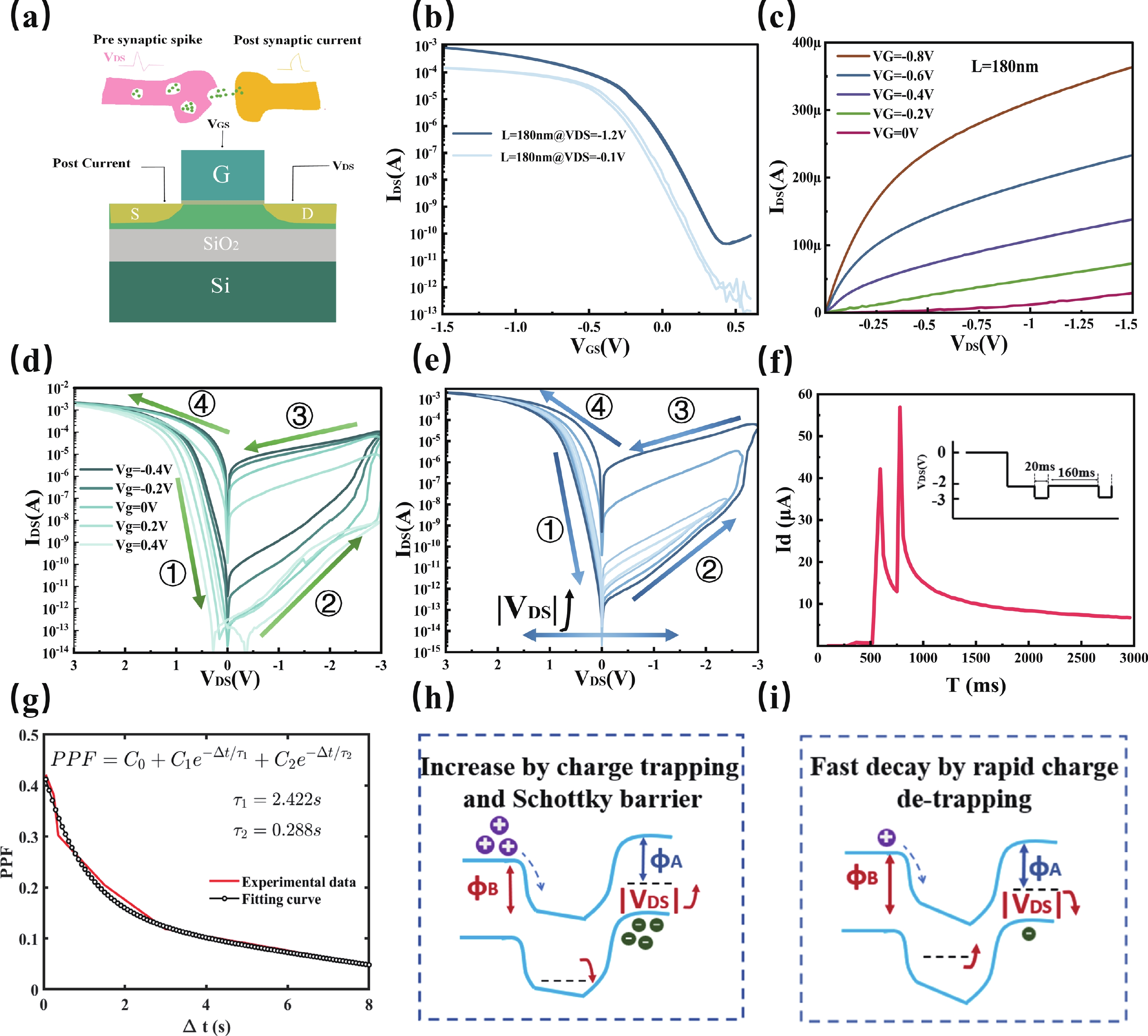
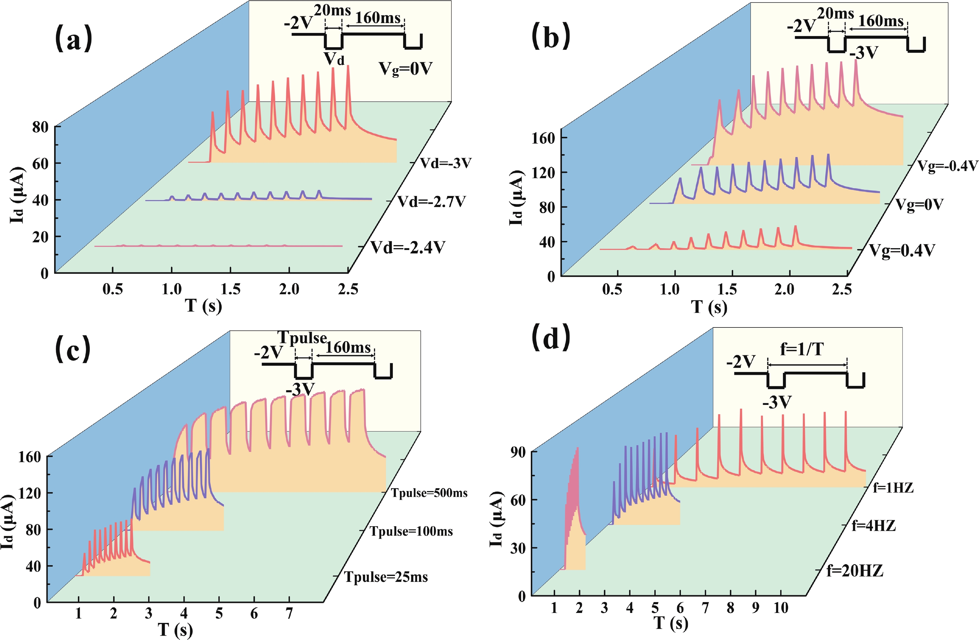
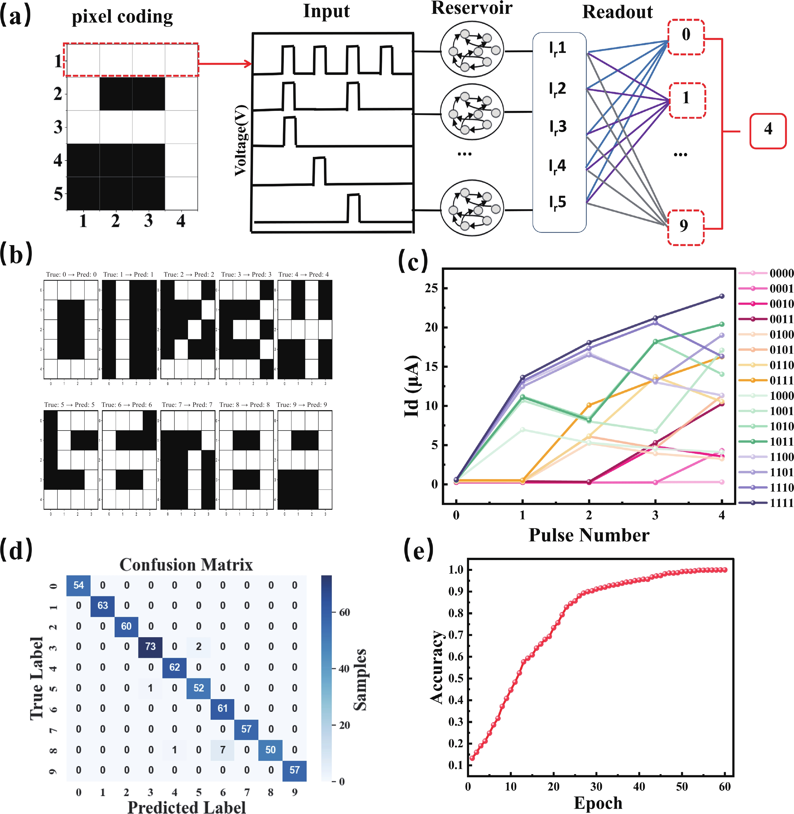
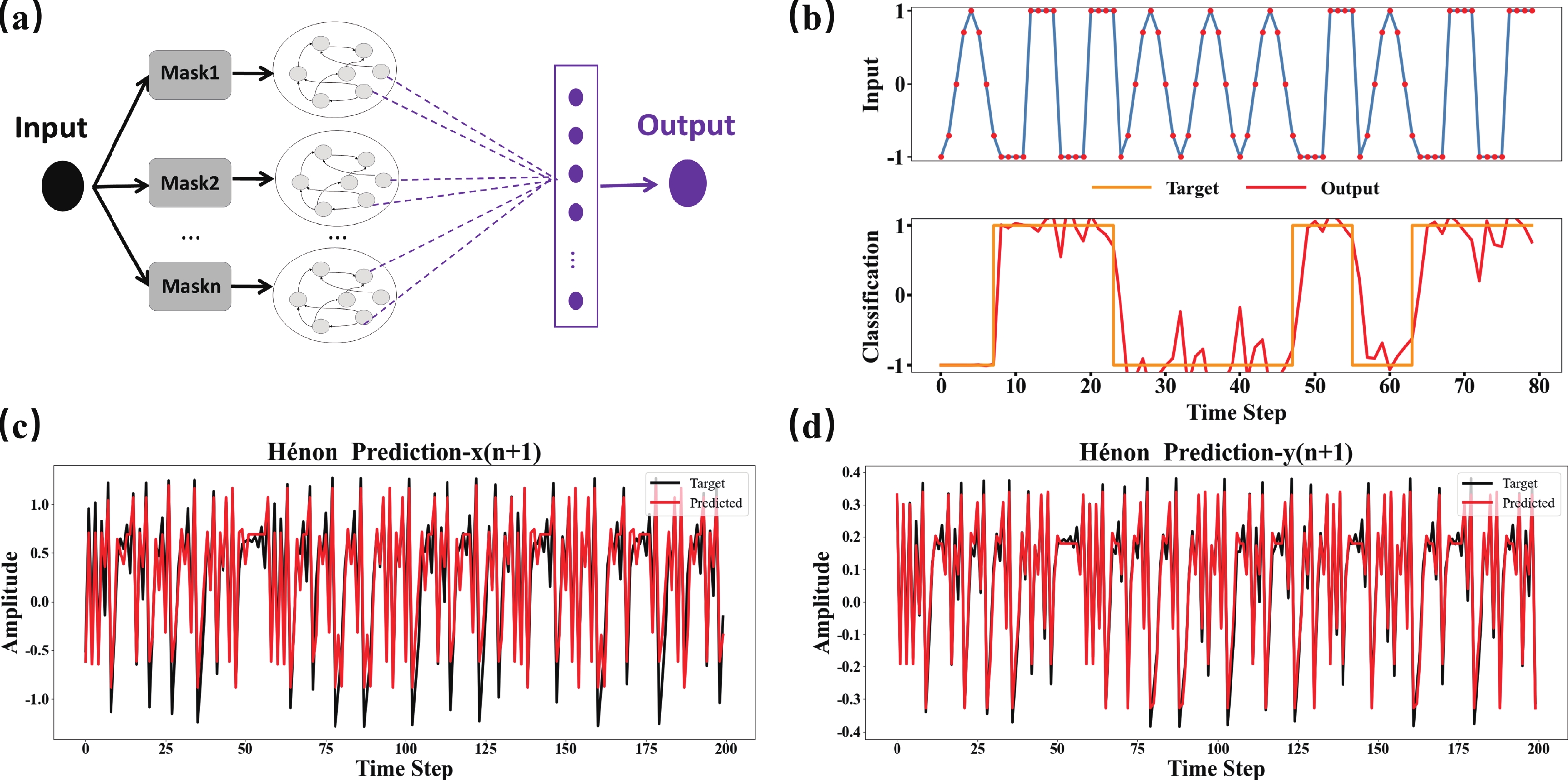
Neuromorphic devices have garnered significant attention as potential building blocks for energy-efficient hardware systems owing to their capacity to emulate the computational efficiency of the brain. In this regard, reservoir computing (RC) framework, which leverages straightforward training methods and efficient temporal signal processing, has emerged as a promising scheme. While various physical reservoir devices, including ferroelectric, optoelectronic, and memristor-based systems, have been demonstrated, many still face challenges related to compatibility with mainstream complementary metal oxide semiconductor (CMOS) integration processes. This study introduced a silicon-based schottky barrier metal−oxide−semiconductor field effect transistor (SB-MOSFET), which was fabricated under low thermal budget and compatible with back-end-of-line (BEOL). The device demonstrated short-term memory characteristics, facilitated by the modulation of schottky barriers and charge trapping. Utilizing these characteristics, a RC system for temporal data processing was constructed, and its performance was validated in a 5 × 4 digital classification task, achieving an accuracy exceeding 98% after 50 training epochs. Furthermore, the system successfully processed temporal signal in waveform classification and prediction tasks using time-division multiplexing. Overall, the SB-MOSFET's high compatibility with CMOS technology provides substantial advantages for large-scale integration, enabling the development of energy-efficient reservoir computing hardware.
J. Semicond.
2026, 47(1): 012401 doi: 10.1088/1674-4926/25030025
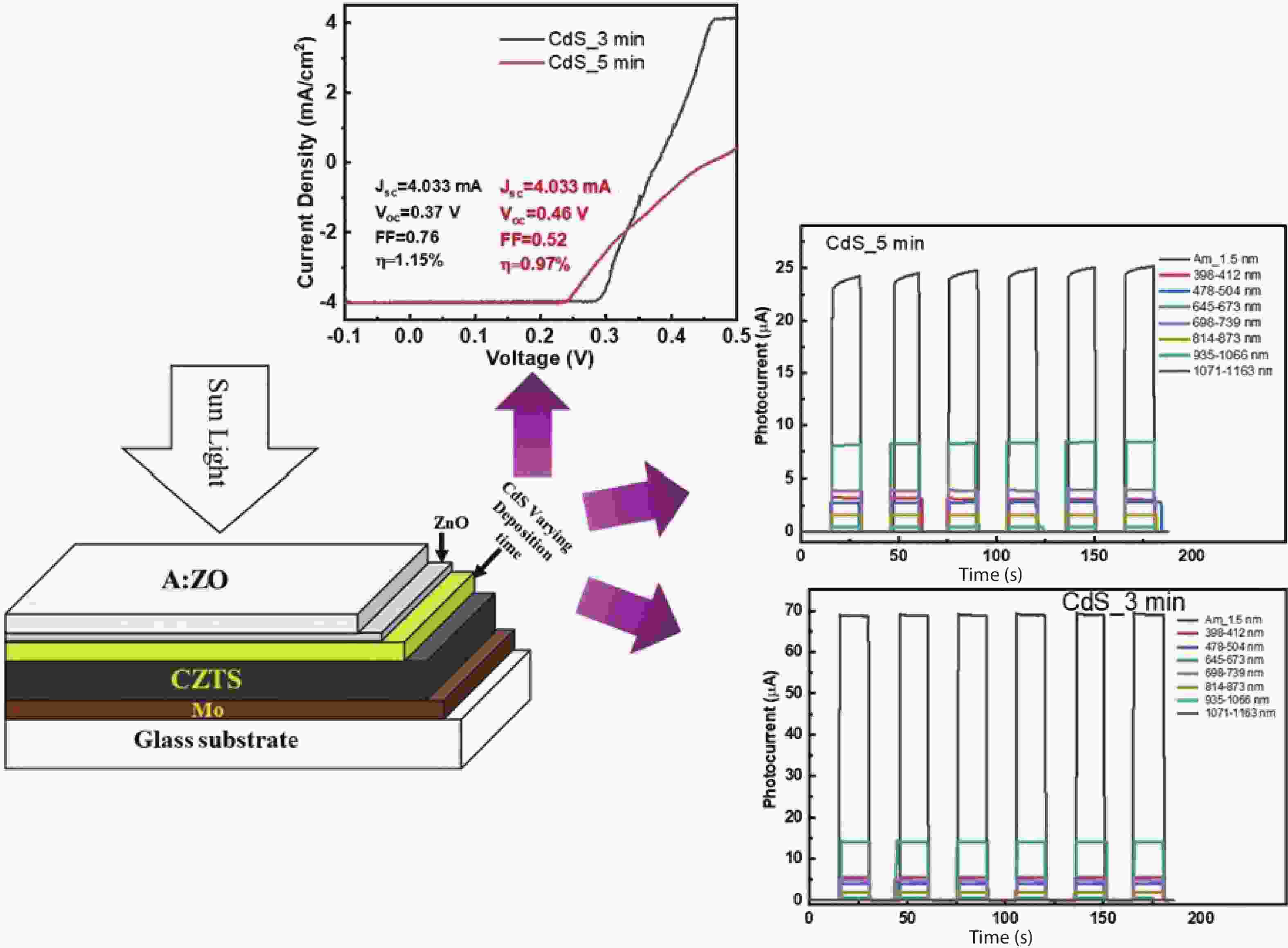
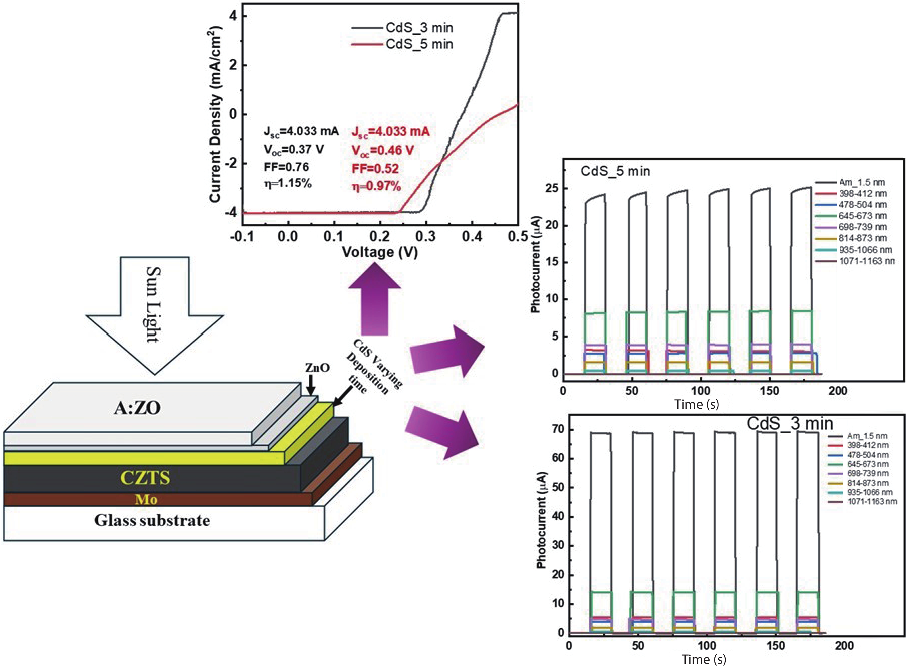
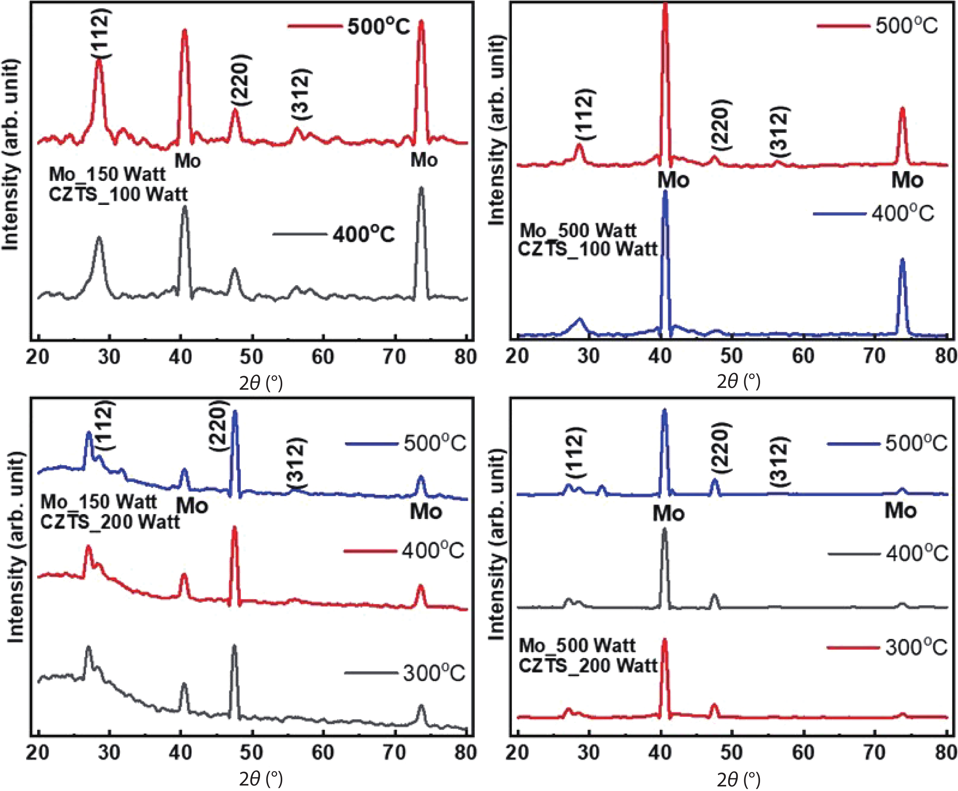
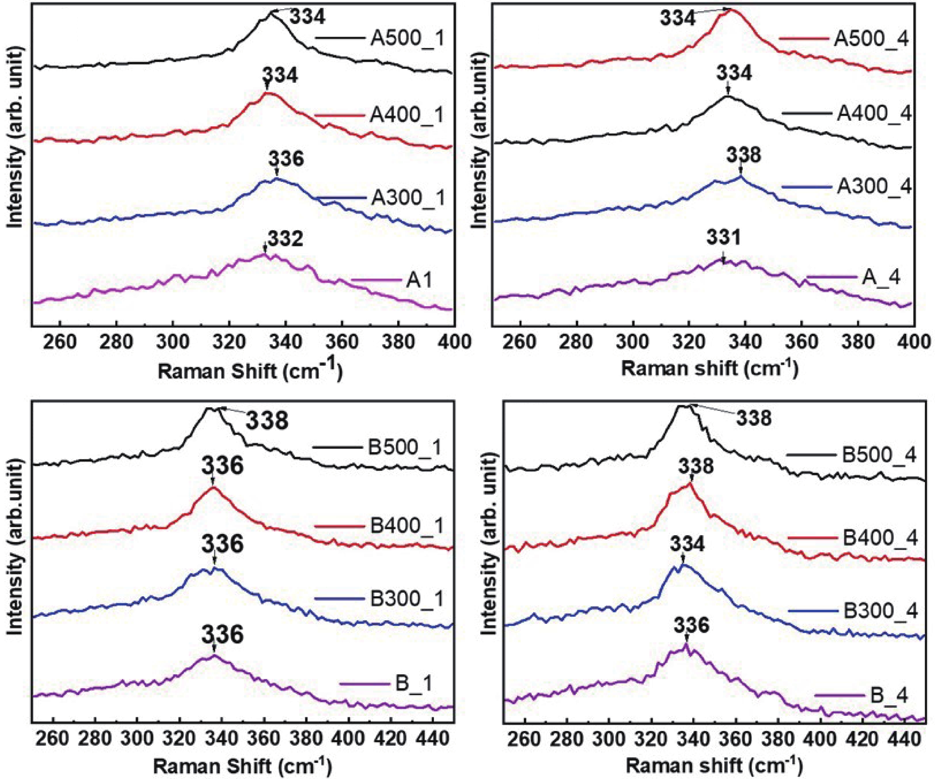
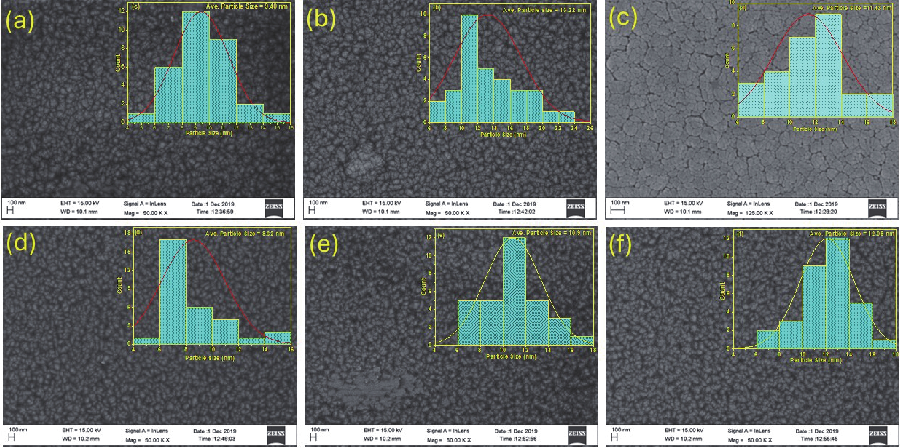
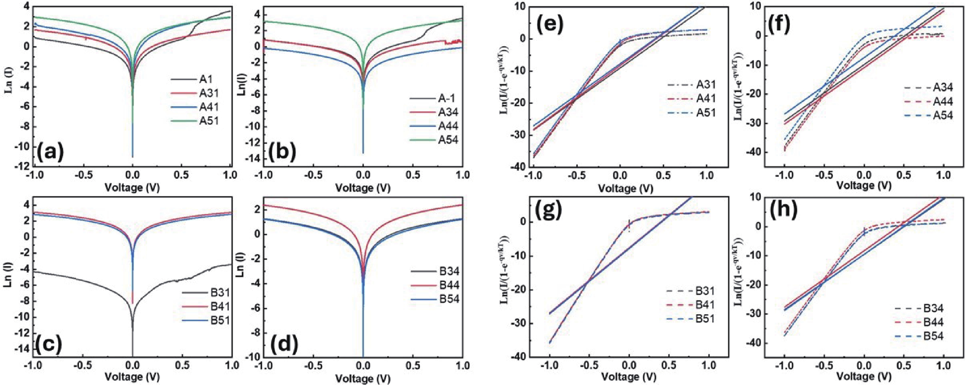
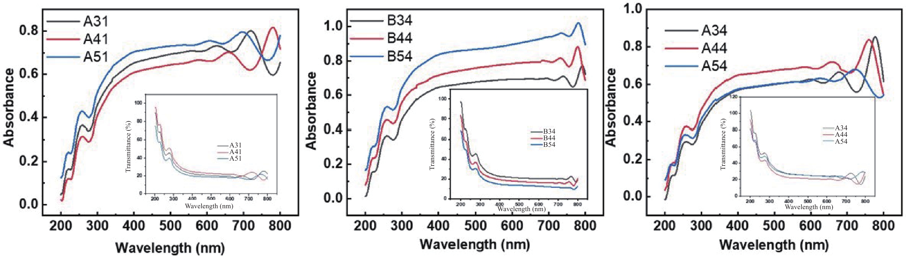
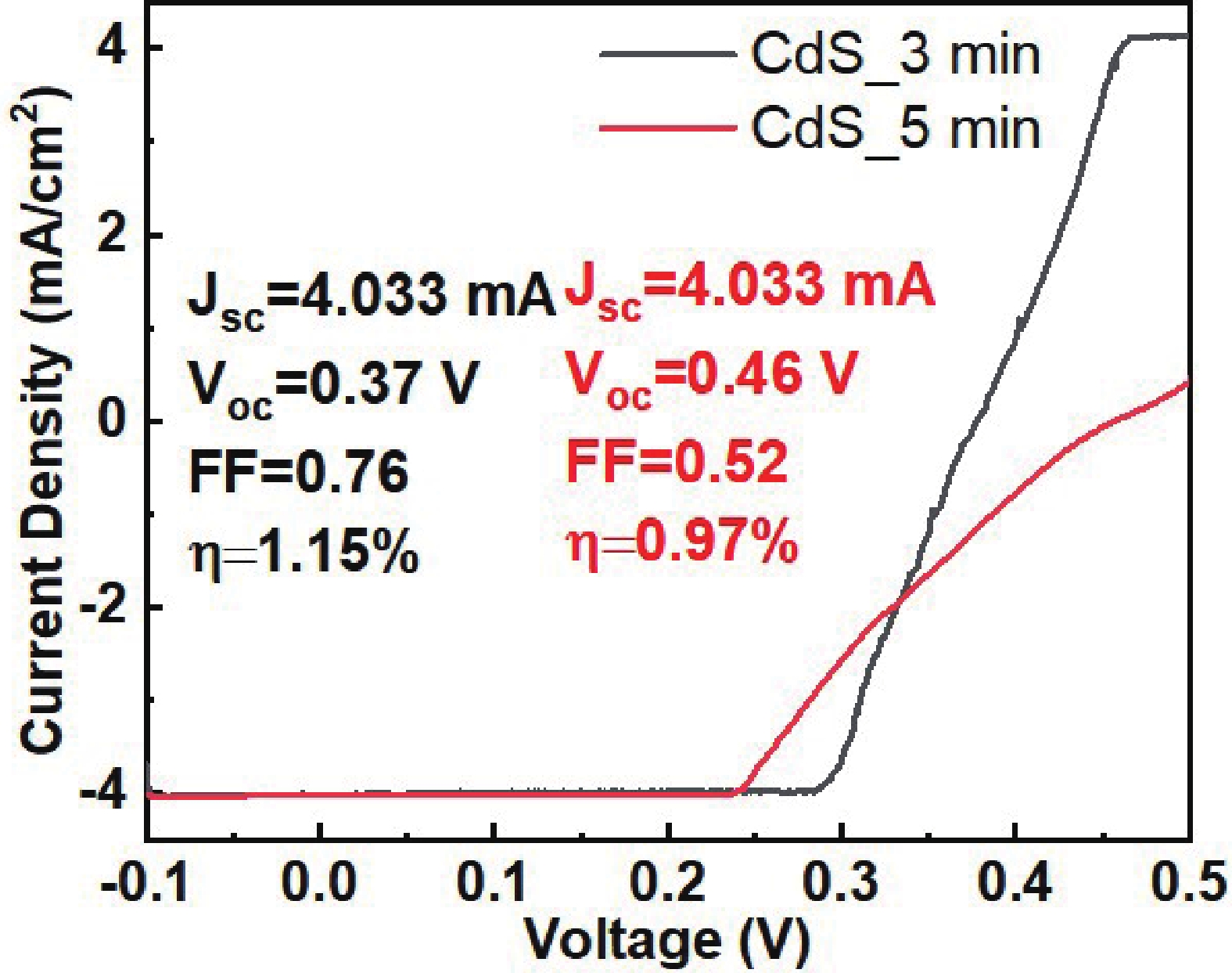
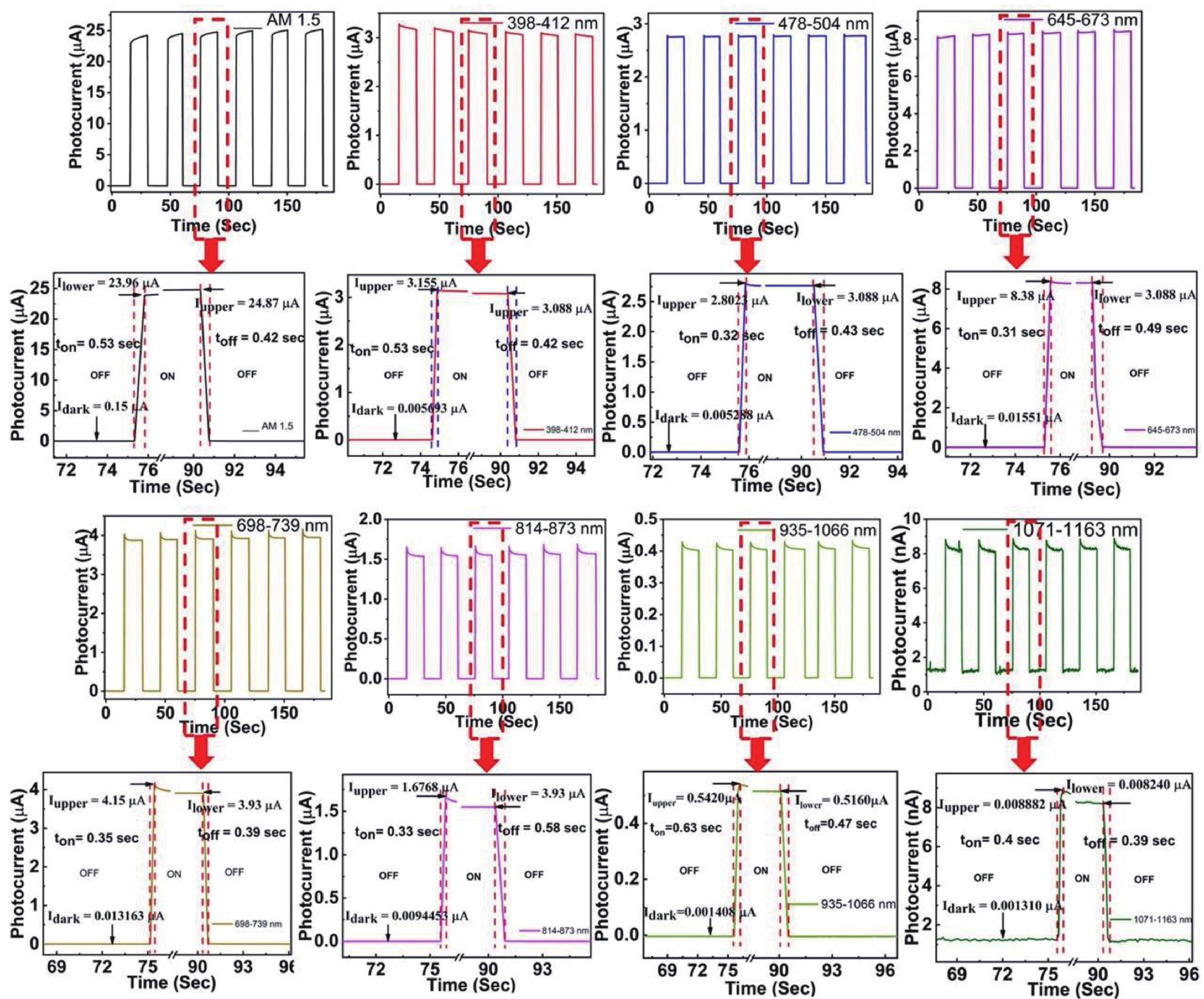
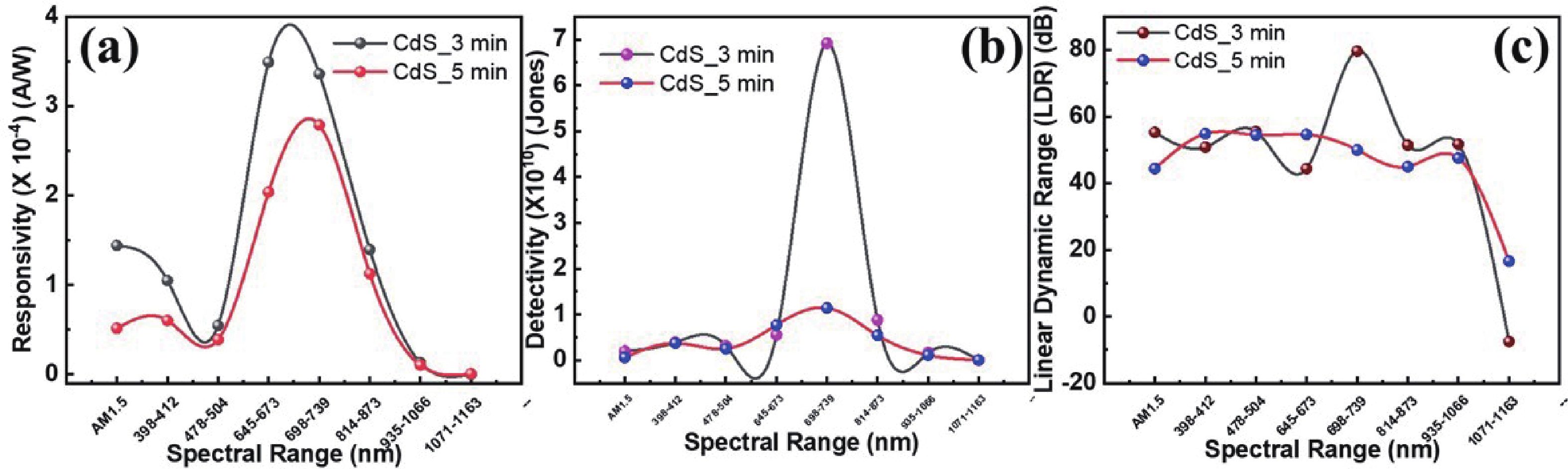
CZTS (Cu2ZnSnS4) is a quaternary semiconductor that is environmentally friendly, less expensive. In this paper, we report on the optimization and fabrication of CZTS-based heterojunction nanodevices for bifunctional applications such as solar cells and photodetectors. CZTS thin films were deposited on top of (Molybdenum) Mo-coated glass substrates via RF sputtering at 100 and 200 W. Rapid thermal processing (RTP) was used at 300, 400, and 500 °C temperatures. CdS (cadmium sulphide) was deposited on CZTS using a chemical bath deposition system with 3- and 5-min deposition times. ZnO (zinc oxide) and AZO (aluminium doped zinc oxide) layers were deposited using RF (radio frequency) sputtering to create the solar device. XRD confirms the formation of a tetragonal structure with increased crystallinity due to the use of RTP. Raman reveals the characteristic Raman shift peak associated with CZTS at 336 and 335 cm−1. The FESEM shows a relationship with RTP temperature. Surface features, including grain size, vary with RTP temperature. The ideality factor is nearly 2, indicating imperfection in the Mo/CZTS interface. Schottky barrier height estimates range from 0.6 to 0.7 eV. Absorbance and transmittance show a predictable fluctuation with RTP temperature. Photovoltaic device was built using the higher crystalline feature of CZTS in conjunction with CdS deposited at 3 and 5 min. The efficiency of CdS deposited after 3 and 5 min was 1.15 and 0.97 percent, respectively. Fabricated devices were used for wavelength-dependent photodetection. This work demonstrated self-powered photodetection.

J. Semicond.
2026, 47(1): 012402 doi: 10.1088/1674-4926/25060004
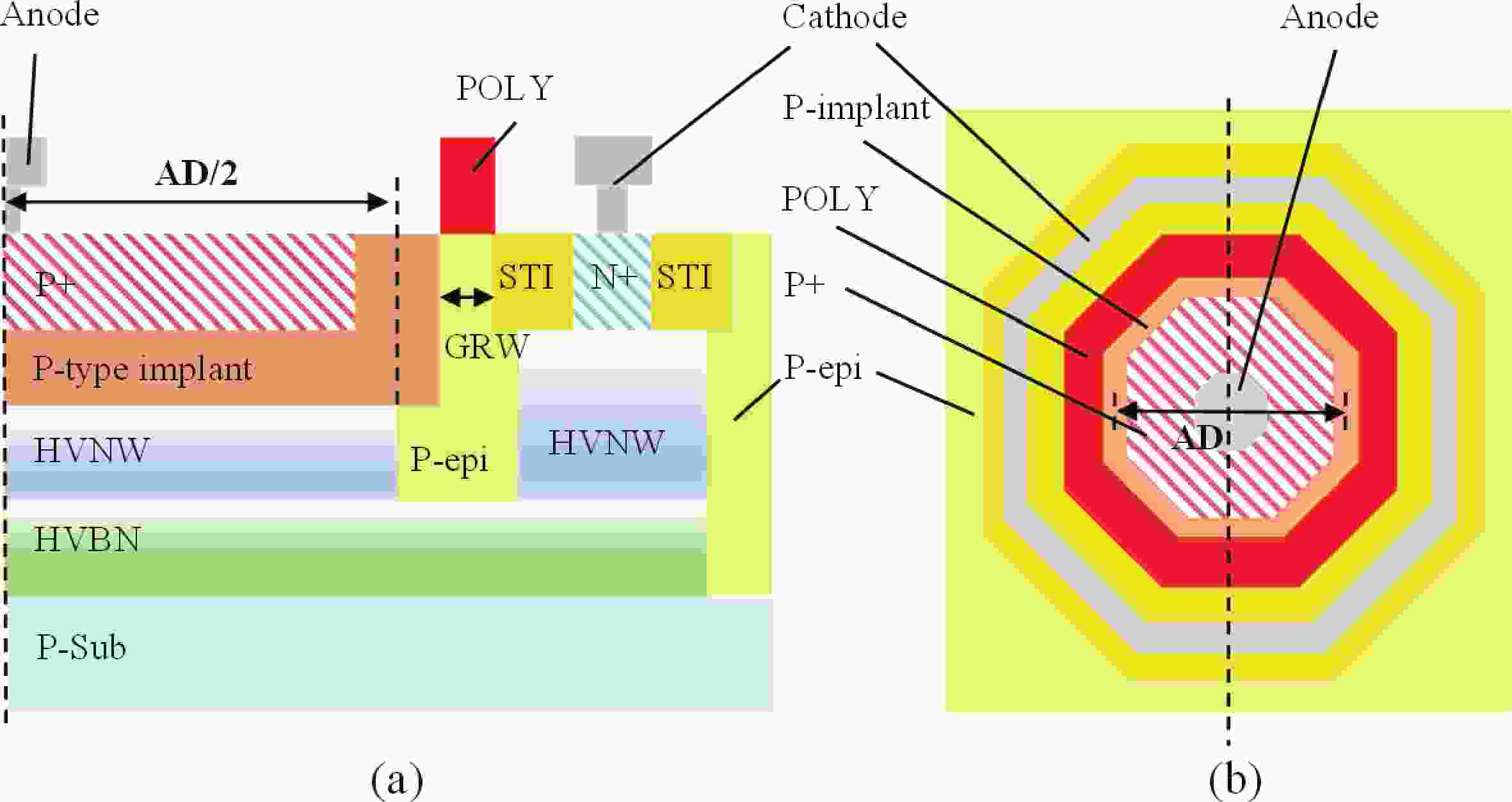
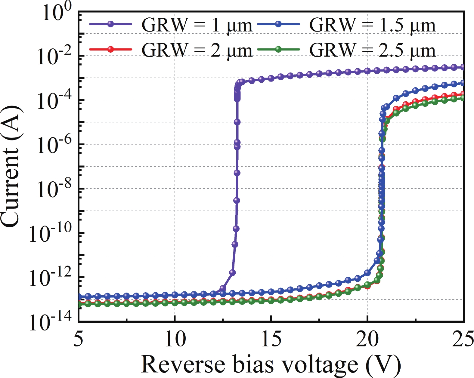
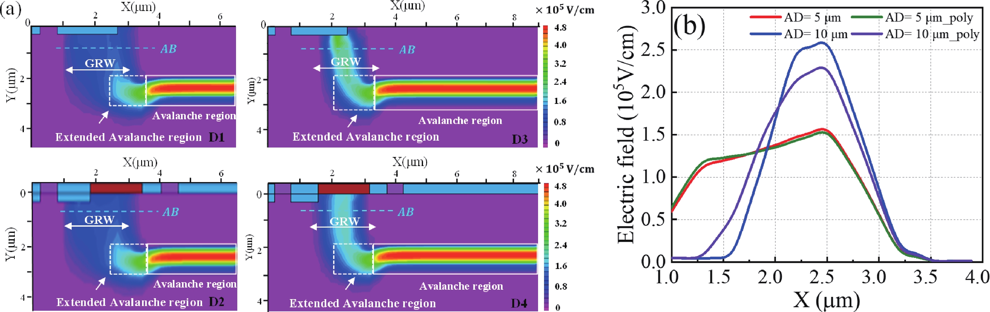
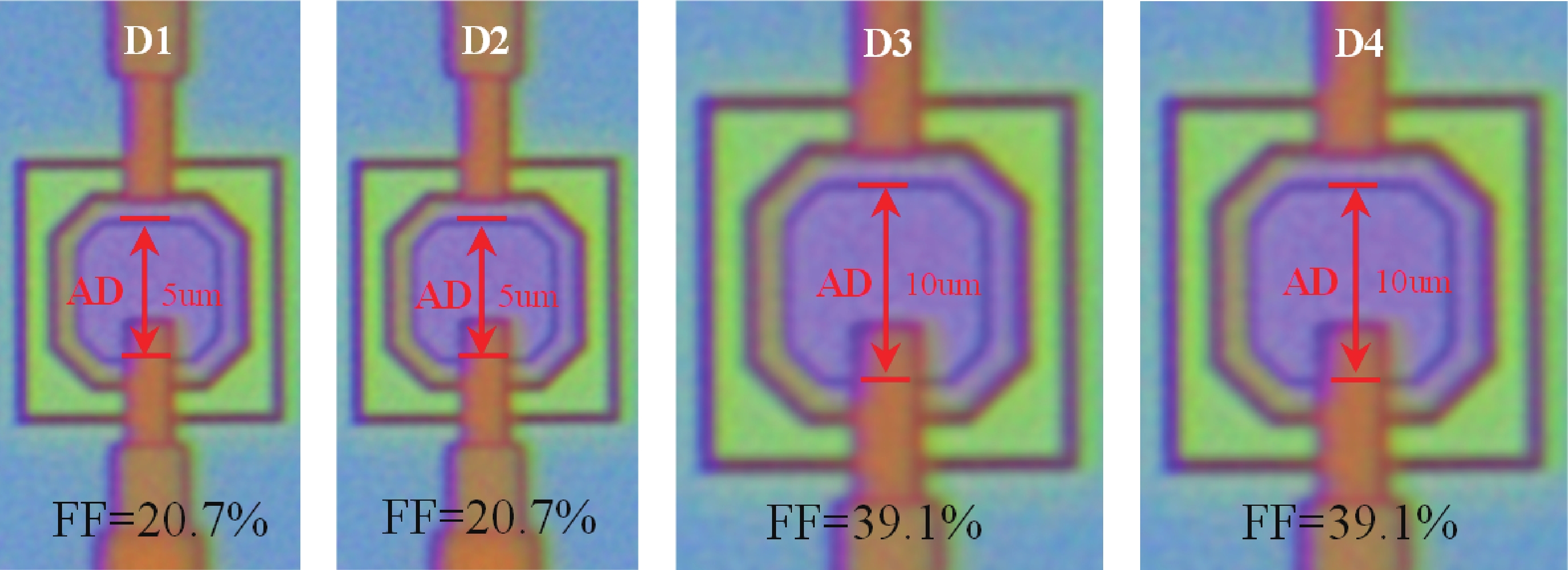
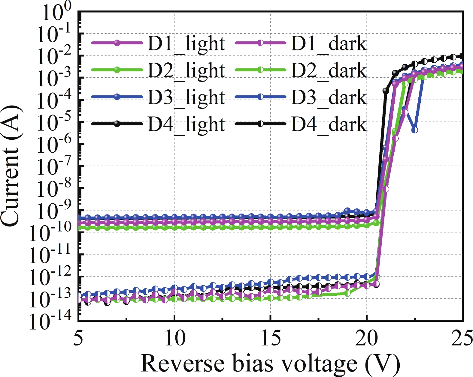
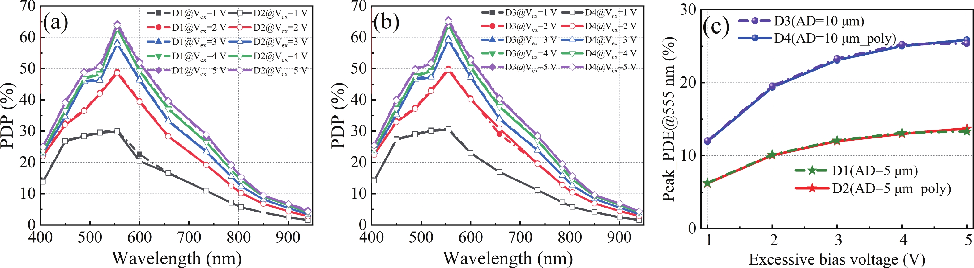
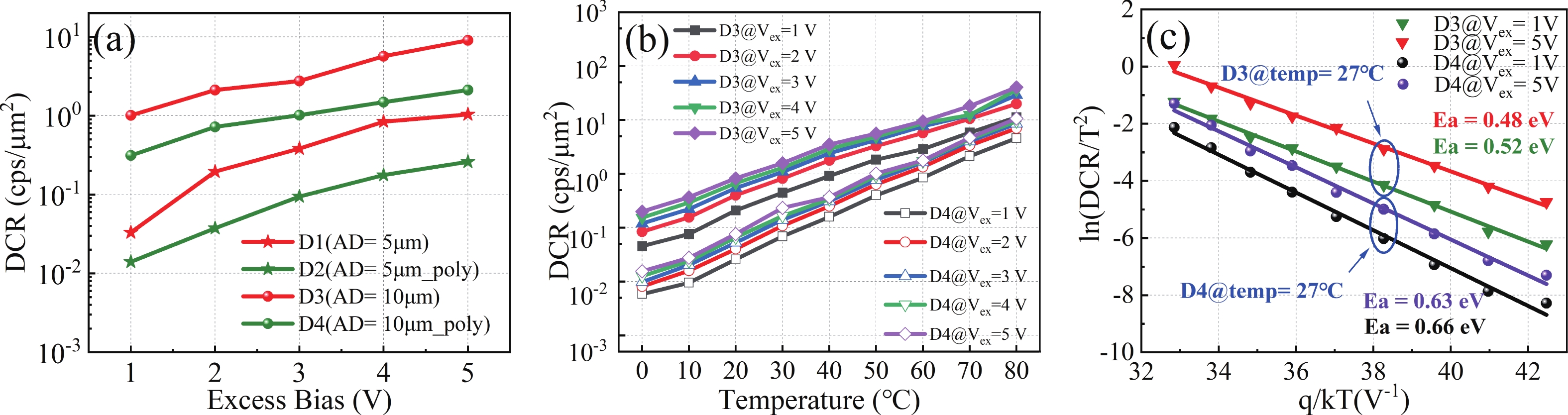
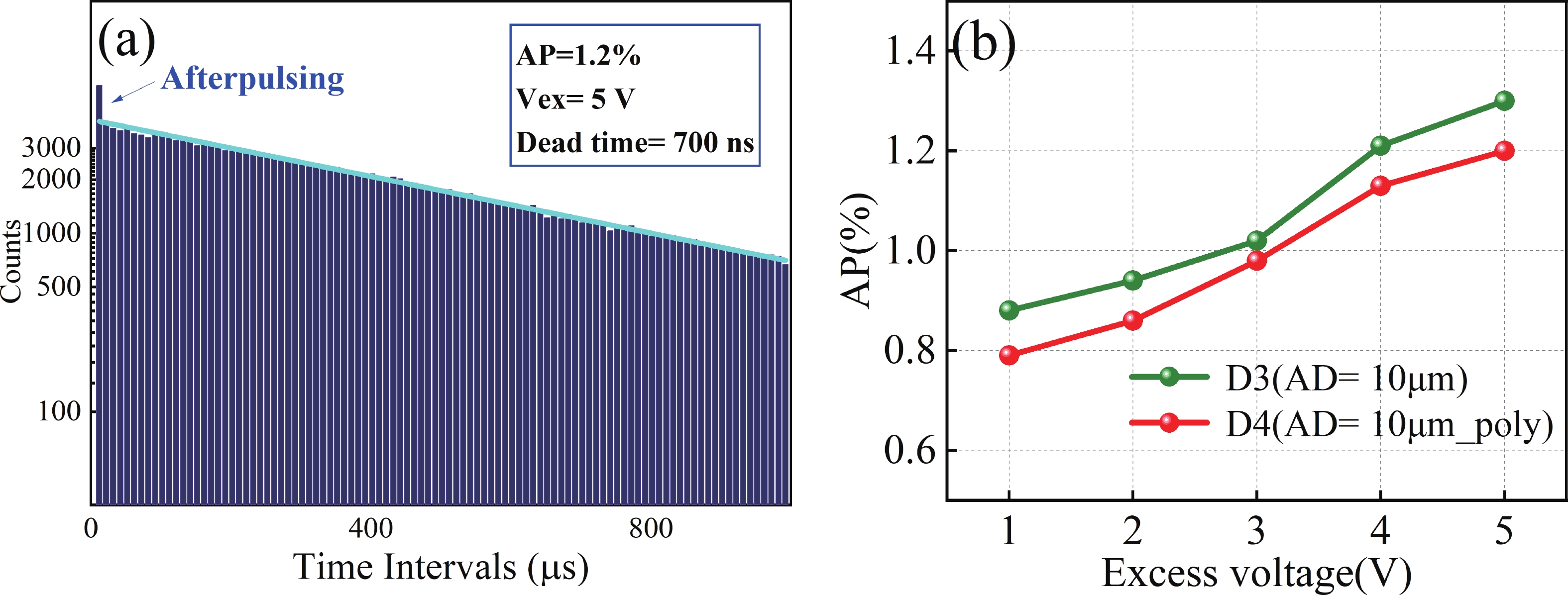
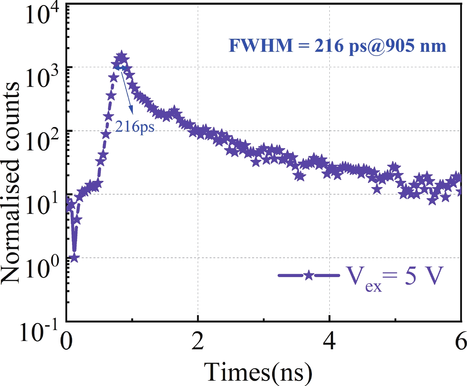
A high-sensitivity, low-noise single photon avalanche diode (SPAD) detector was presented based on a 180 nm BCD process. The proposed device utilizes a p-implant layer/high-voltage n-well (HVNW) junction to form a deep avalanche multiplication region for near-infrared (NIR) sensitivity enhancement. By optimizing the device size and electric field of the guard ring, the fill factor (FF) is significantly improved, further increasing photon detection efficiency (PDE). To solve the dark noise caused by the increasing active diameter, a field polysilicon gate structure connected to the p+ anode was investigated, effectively suppressing dark count noise by 76.6%. It is experimentally shown that when the active diameter increases from 5 to 10 μm, the FF is significantly improved from 20.7% to 39.1%, and thus the peak PDE also rises from 13.3% to 25.8%. At an excess bias voltage of 5 V, a NIR photon detection probability (PDP) of 6.8% at 905 nm, a dark count rate (DCR) of 2.12 cps/μm2, an afterpulsing probability (AP) of 1.2%, and a timing jitter of 216 ps are achieved, demonstrating excellent single photon detection performance.
J. Semicond.
2026, 47(1): 012403 doi: 10.1088/1674-4926/25060032
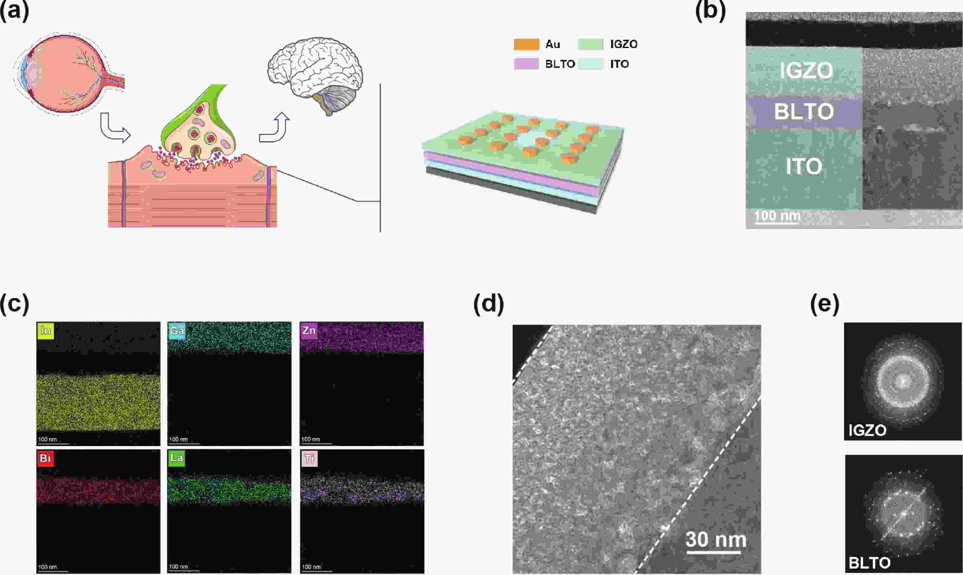
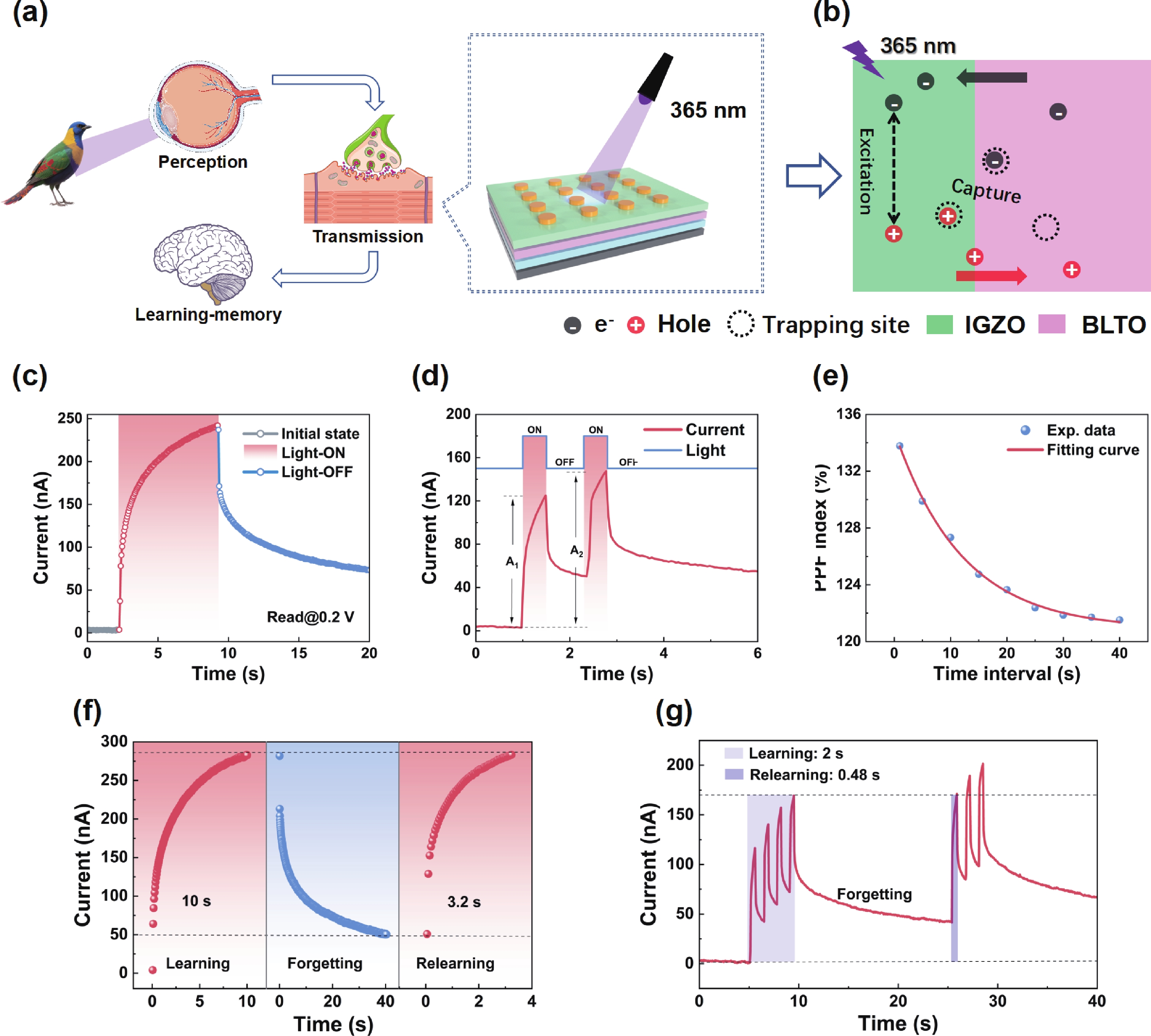
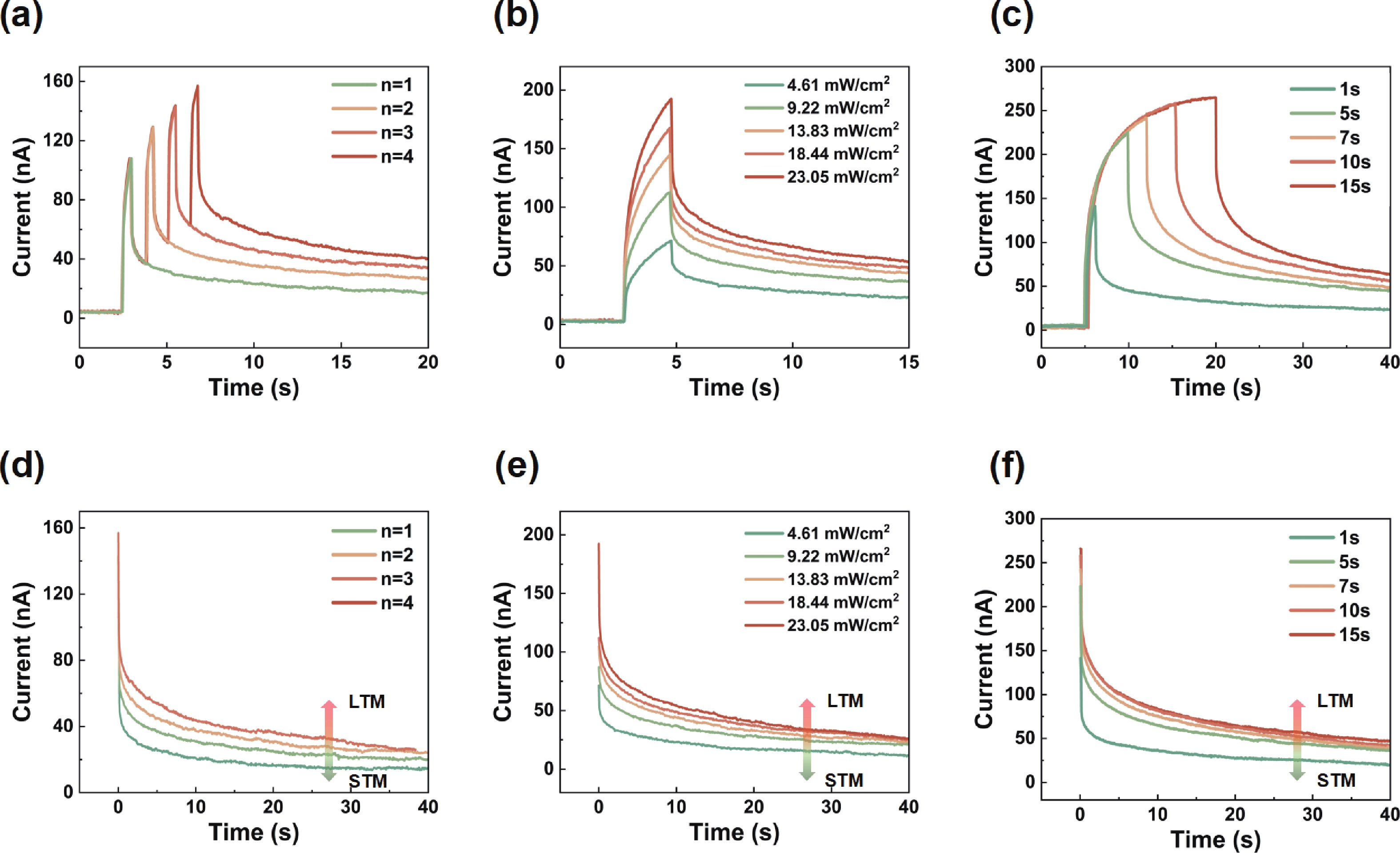
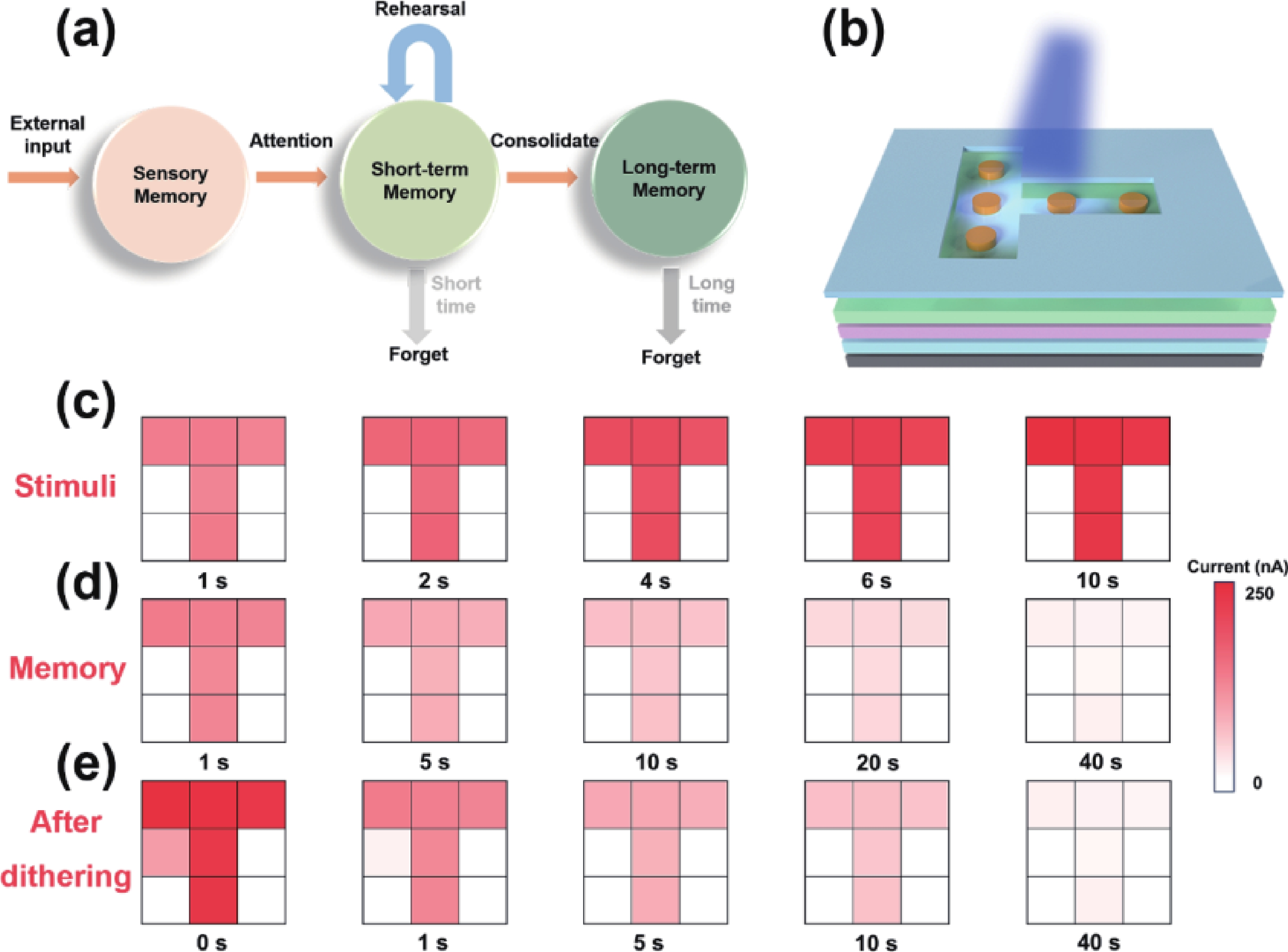
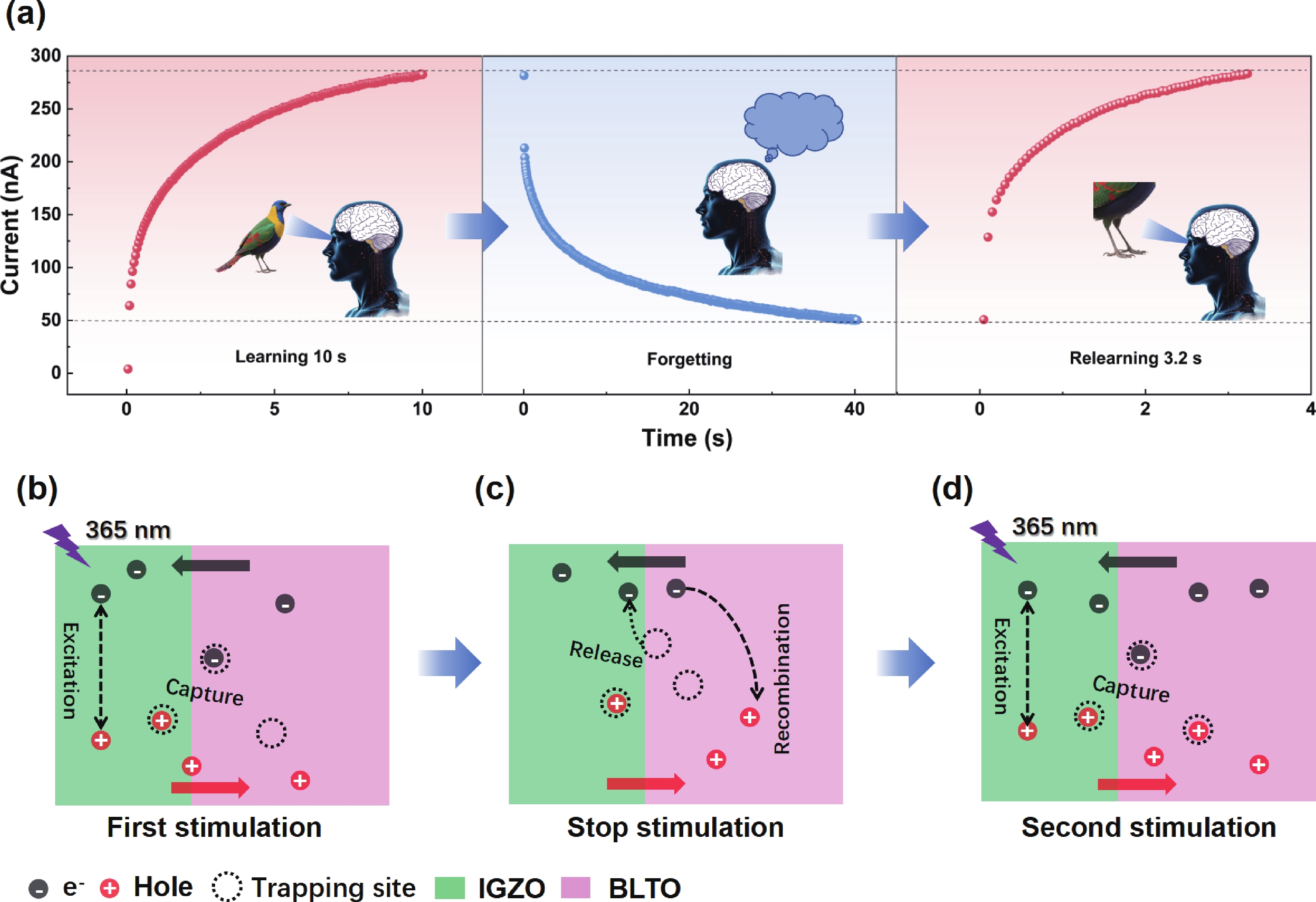
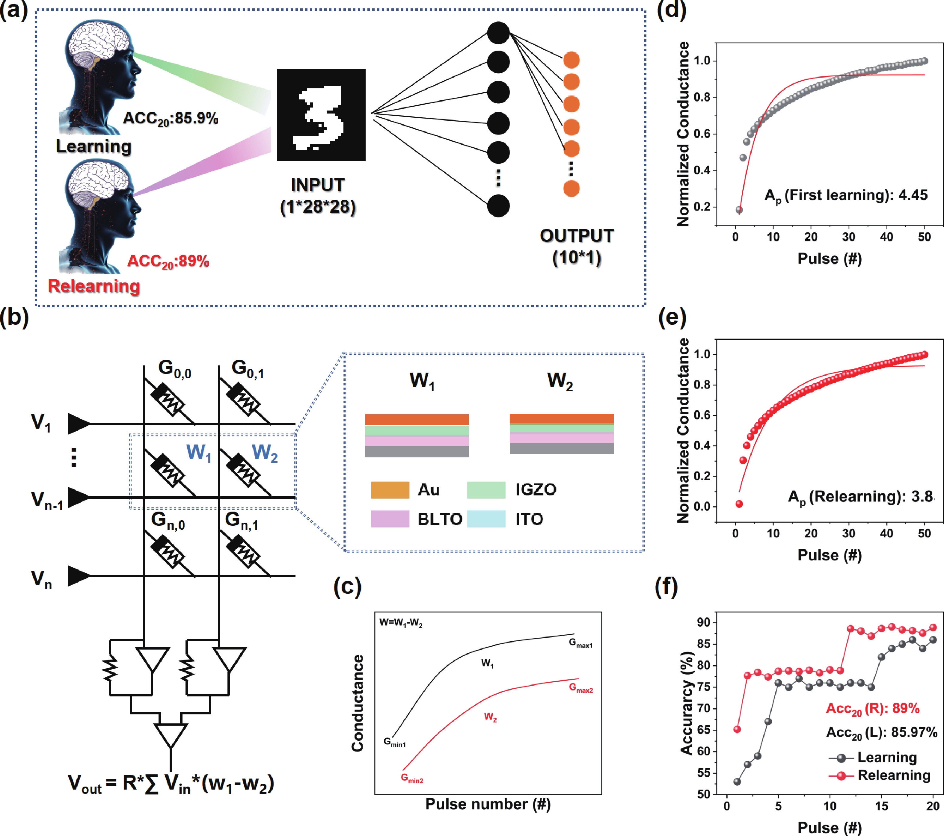
In recent years, optoelectronic synapses have garnered significant attention in the field of neuromorphic computing due to their integration of optical sensing and synaptic functions. In this work, we propose an optoelectronic synapse based on IGZO/Bi3.25La0.75Ti3O12 heterojunction. Under UV light stimulation, this device can simulate a range of synaptic behaviors, including paired-pulse facilitation, spike-intensity-dependent plasticity, spike-number-dependent plasticity, spike-width-dependent plasticity, and the transition from short-term memory to long-term memory. The majority of perceptible information for humans is acquired through the visual system. The 3 × 3 retinal morphology synapse arrays constructed based on plasticity behaviors not only integrates light perception and storage functions but also exhibits adaptive adjustment capabilities to address image blurring caused by object movement. At the same time, in CNN recognition training, the device successfully simulates the learning−relearning mechanism of the human brain. These findings highlight the device’s immense potential for applications in artificial vision systems.
J. Semicond.
2026, 47(1): 012501 doi: 10.1088/1674-4926/25040023
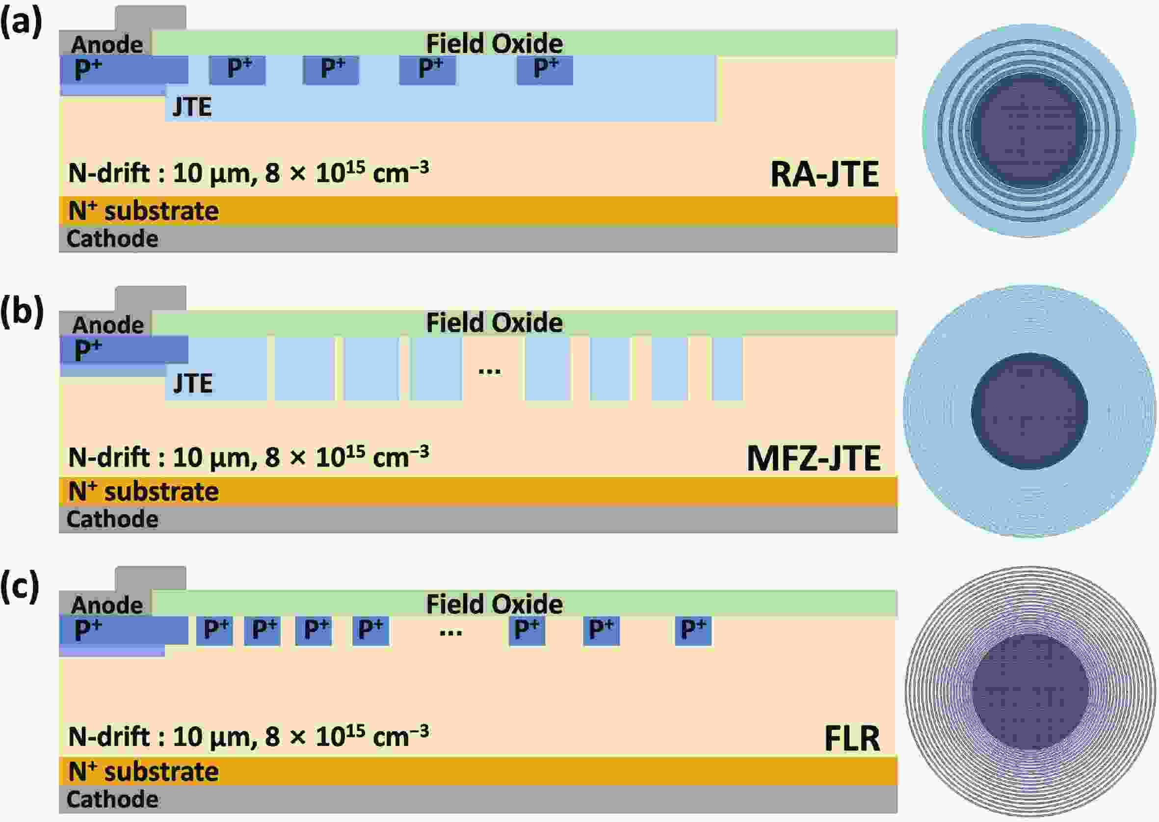
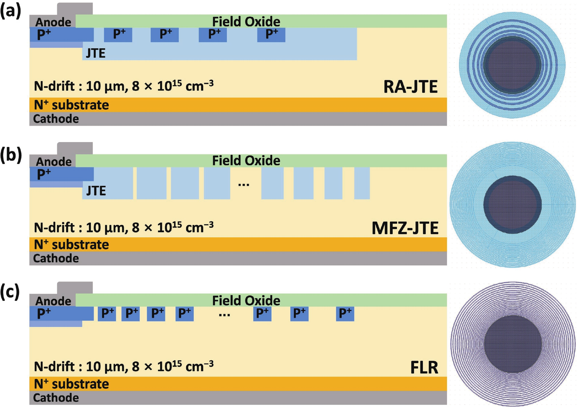
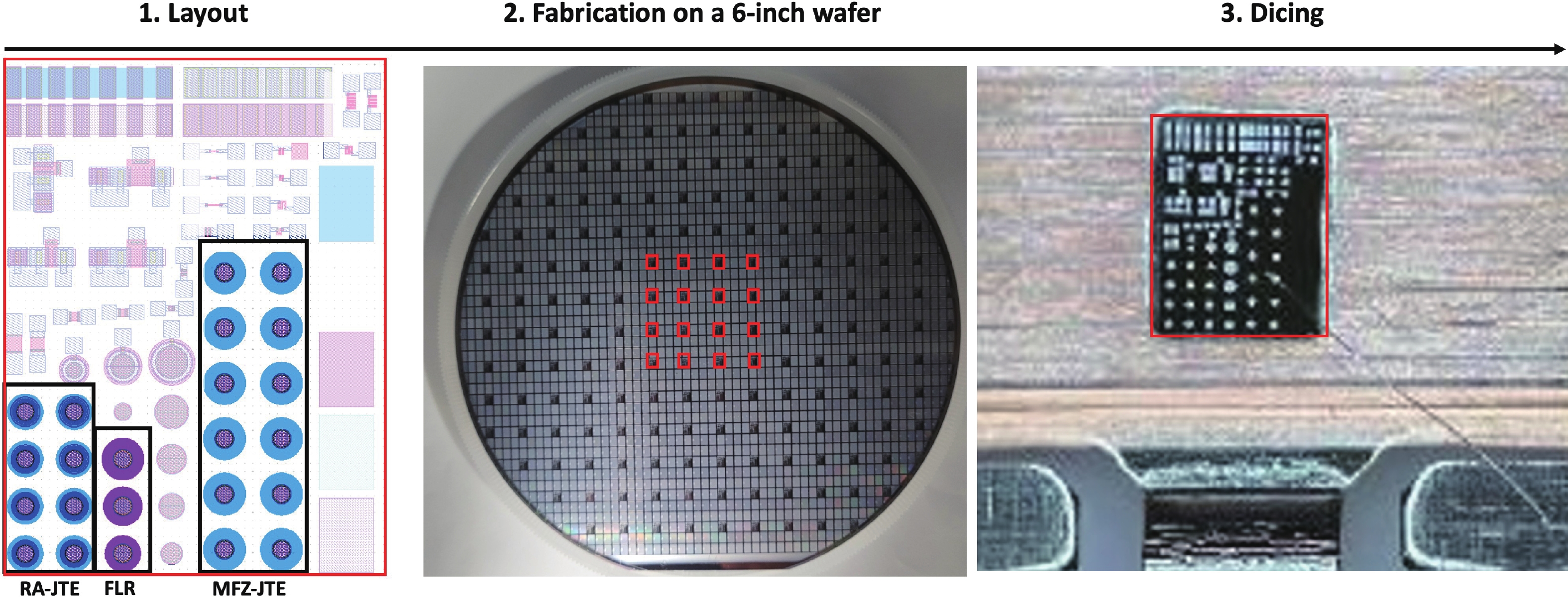
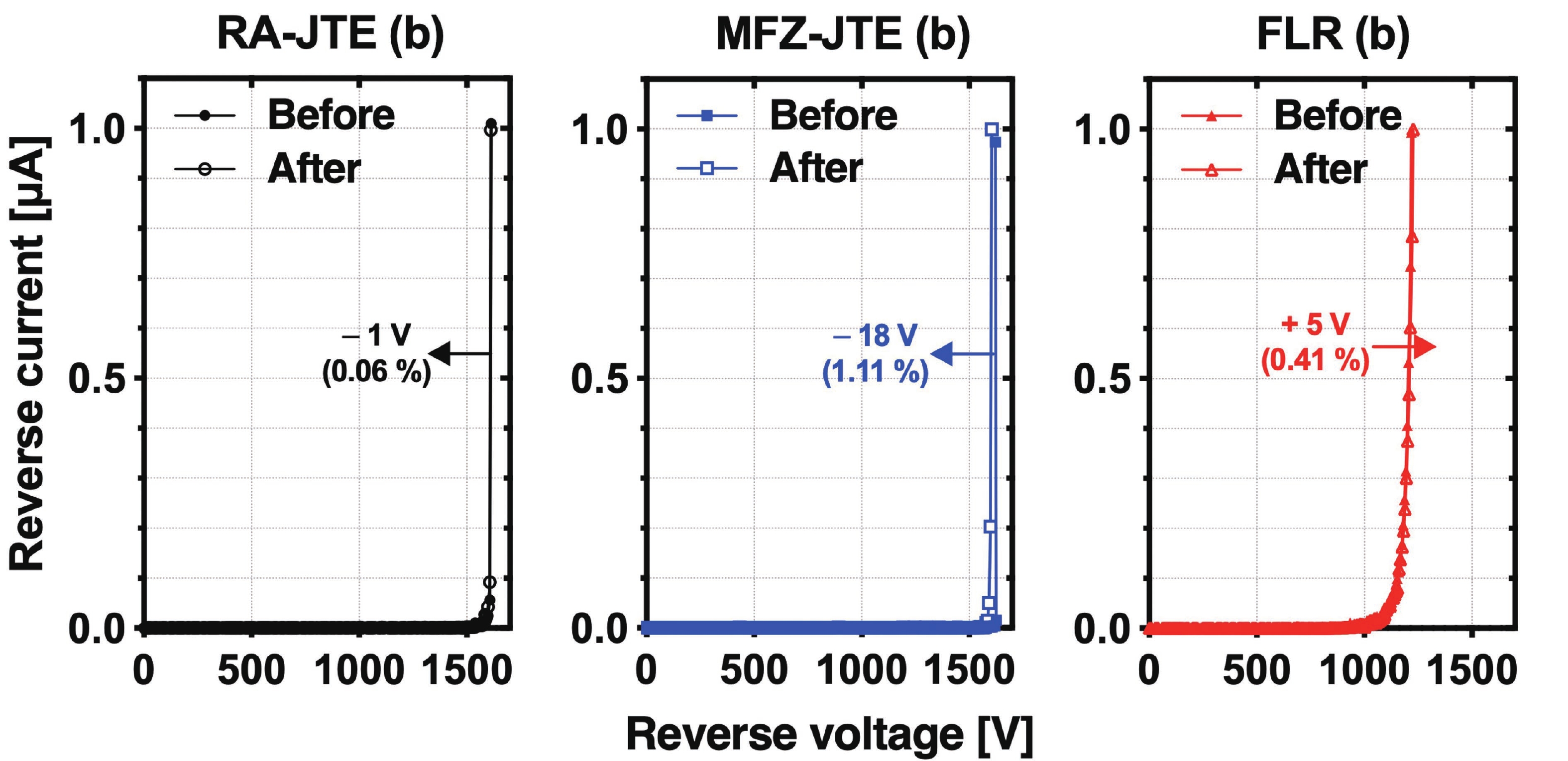
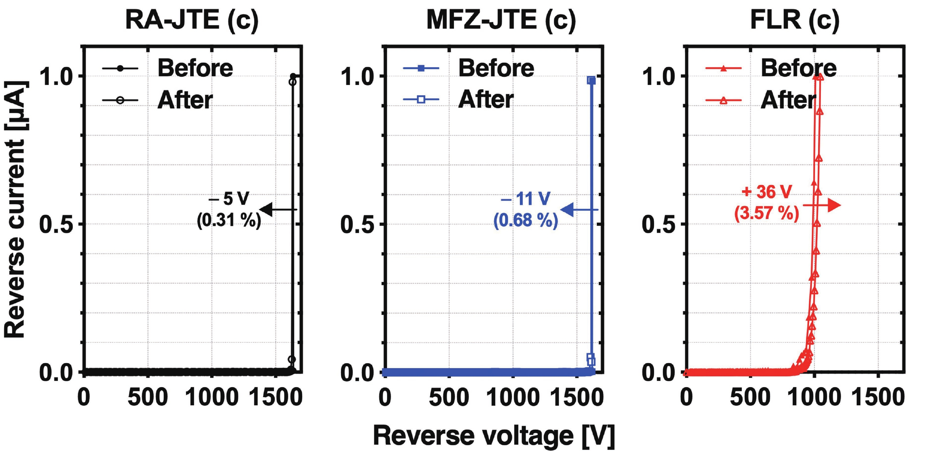
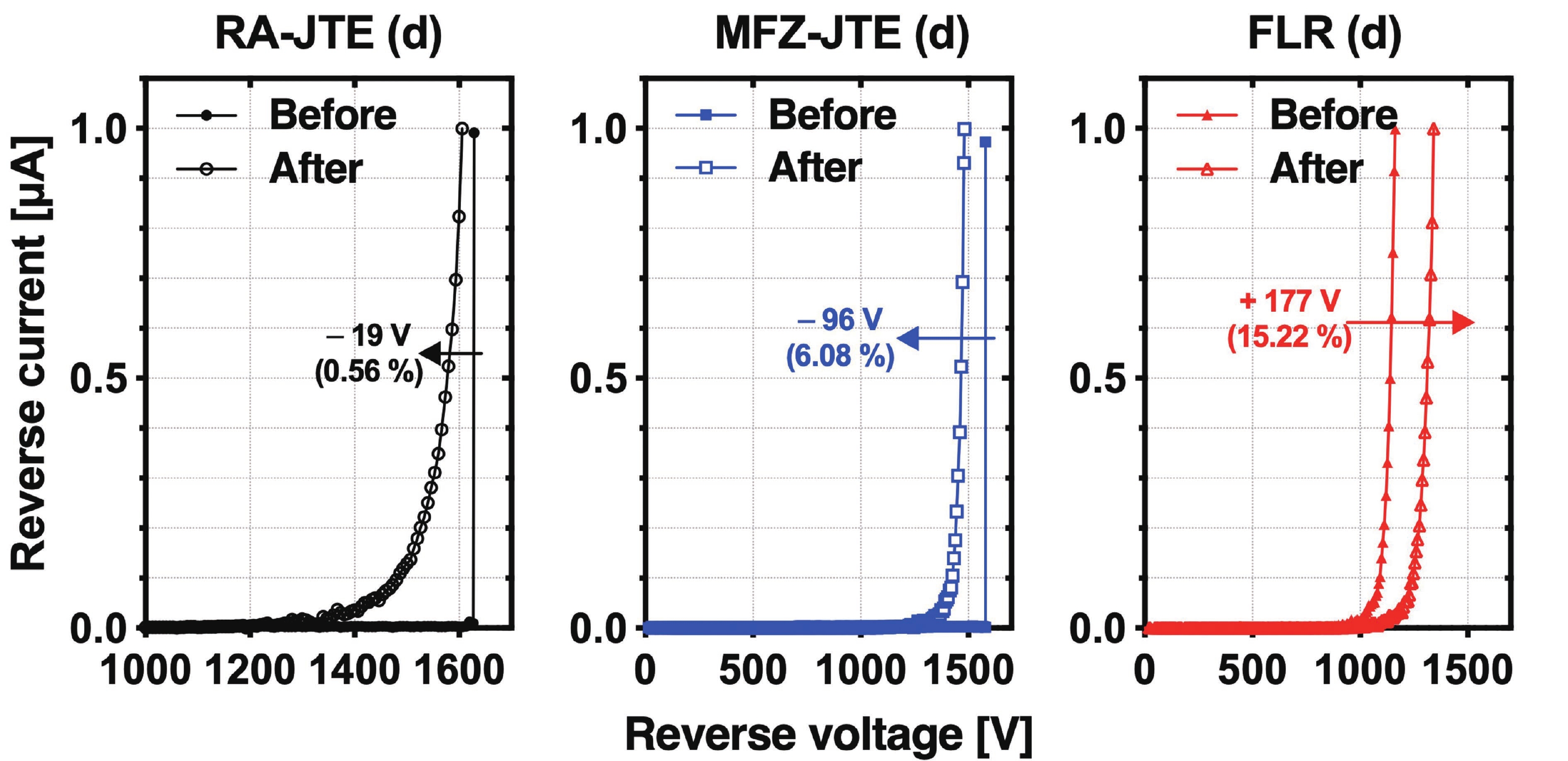
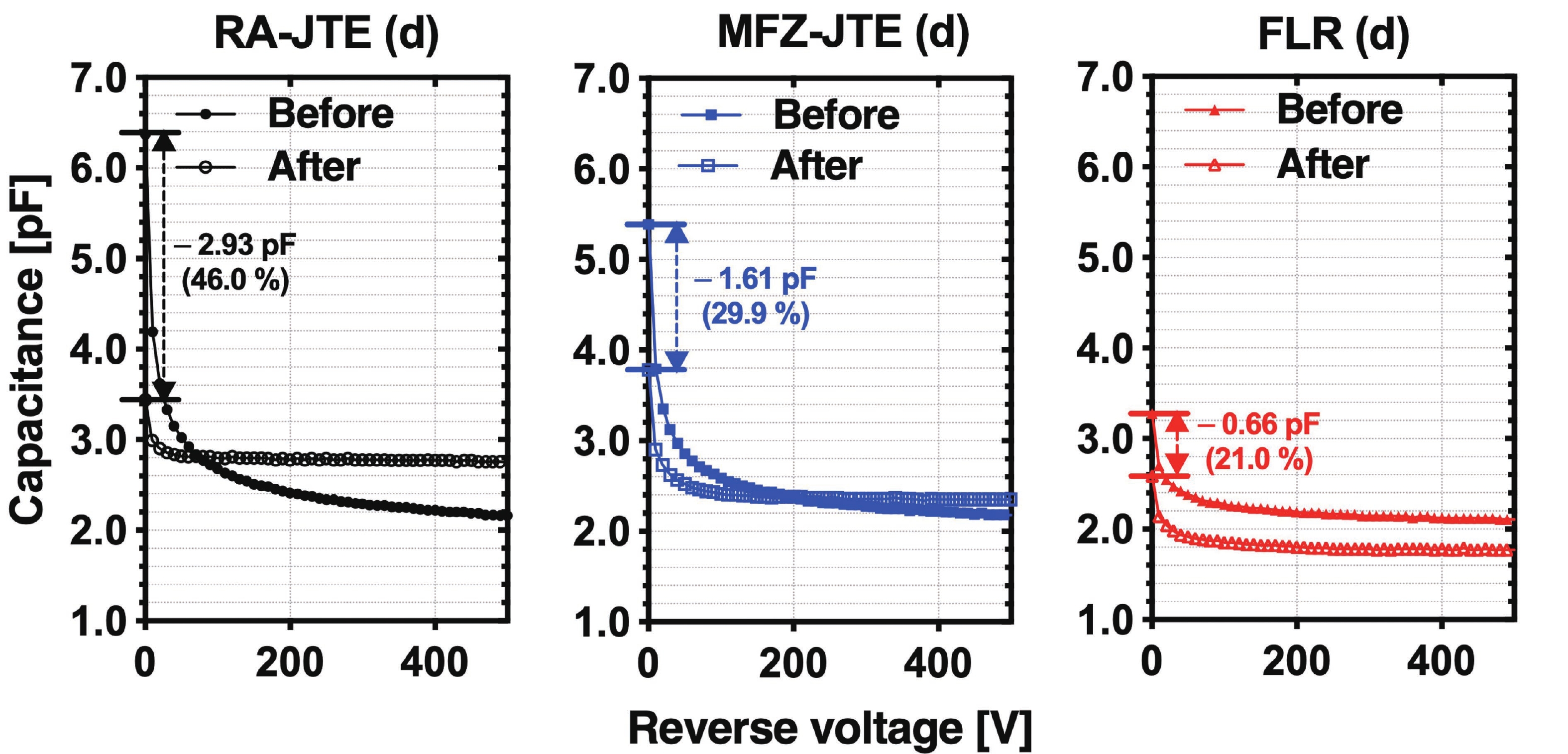
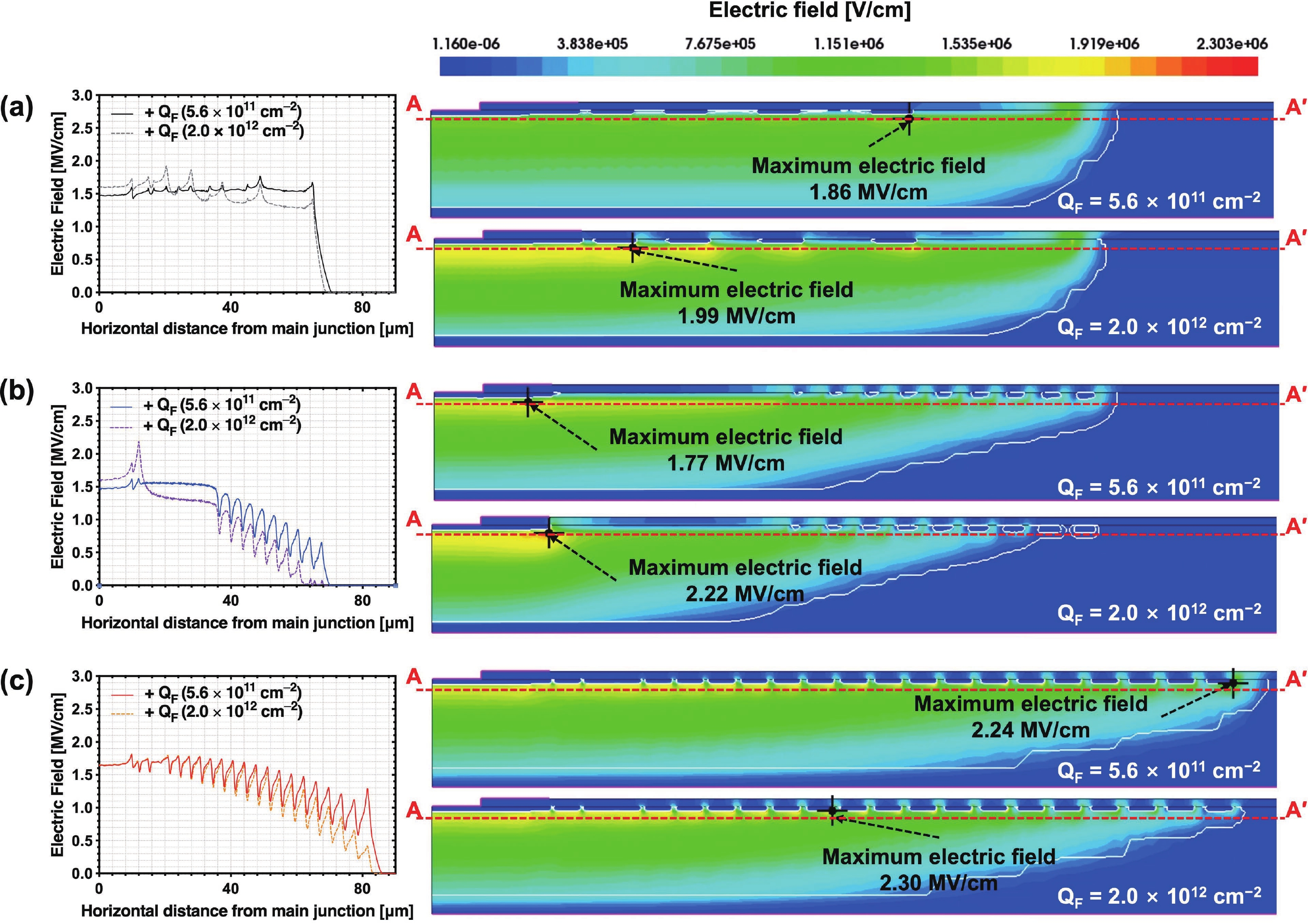
This work presents a systematic analysis of proton-induced total ionizing dose (TID) effects in 1.2 kV silicon carbide (SiC) power devices with various edge termination structures. Three edge terminations including ring-assisted junction termination extension (RA-JTE), multiple floating zone JTE (MFZ-JTE), and field limiting rings (FLR) were fabricated and irradiated with 45 MeV protons at fluences ranging from 1 × 10¹² to 1 × 1014 cm−2. Experimental results, supported by TCAD simulations, show that the RA-JTE structure maintained stable breakdown performance with less than 1% variation due to its effective electric field redistribution by multiple P+ rings. In contrast, MFZ-JTE and FLR exhibit breakdown voltage shifts of 6.1% and 15.2%, respectively, under the highest fluence. These results demonstrate the superior radiation tolerance of the RA-JTE structure under TID conditions and provide practical design guidance for radiation-hardened SiC power devices in space and other high-radiation environments.
J. Semicond.
2026, 47(1): 012502 doi: 10.1088/1674-4926/25110003
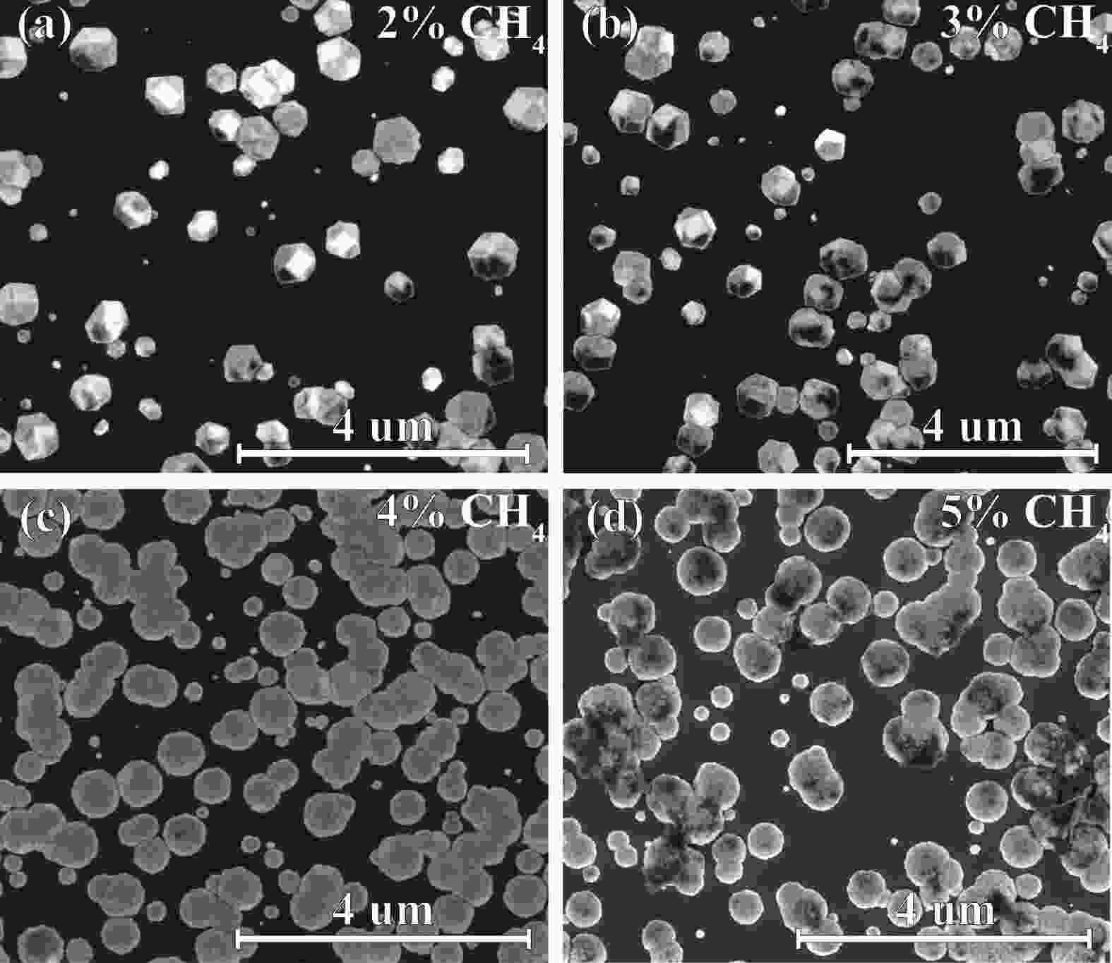
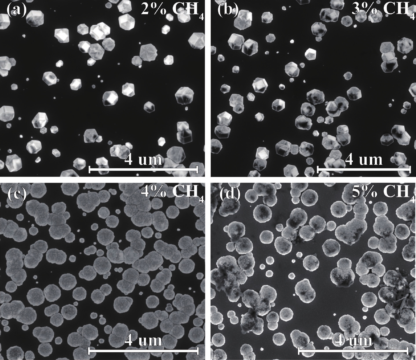
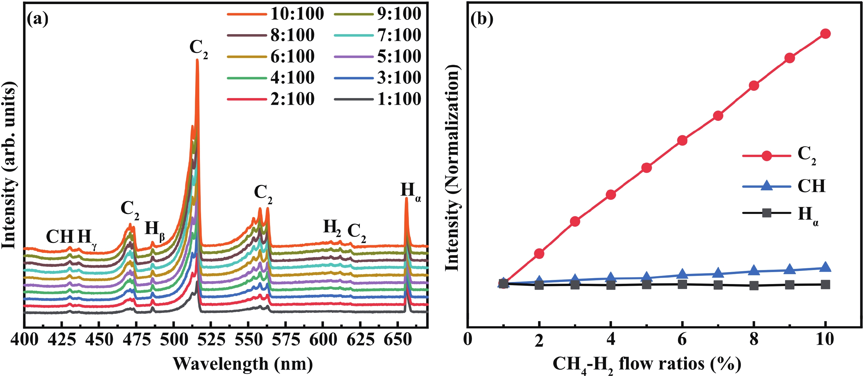
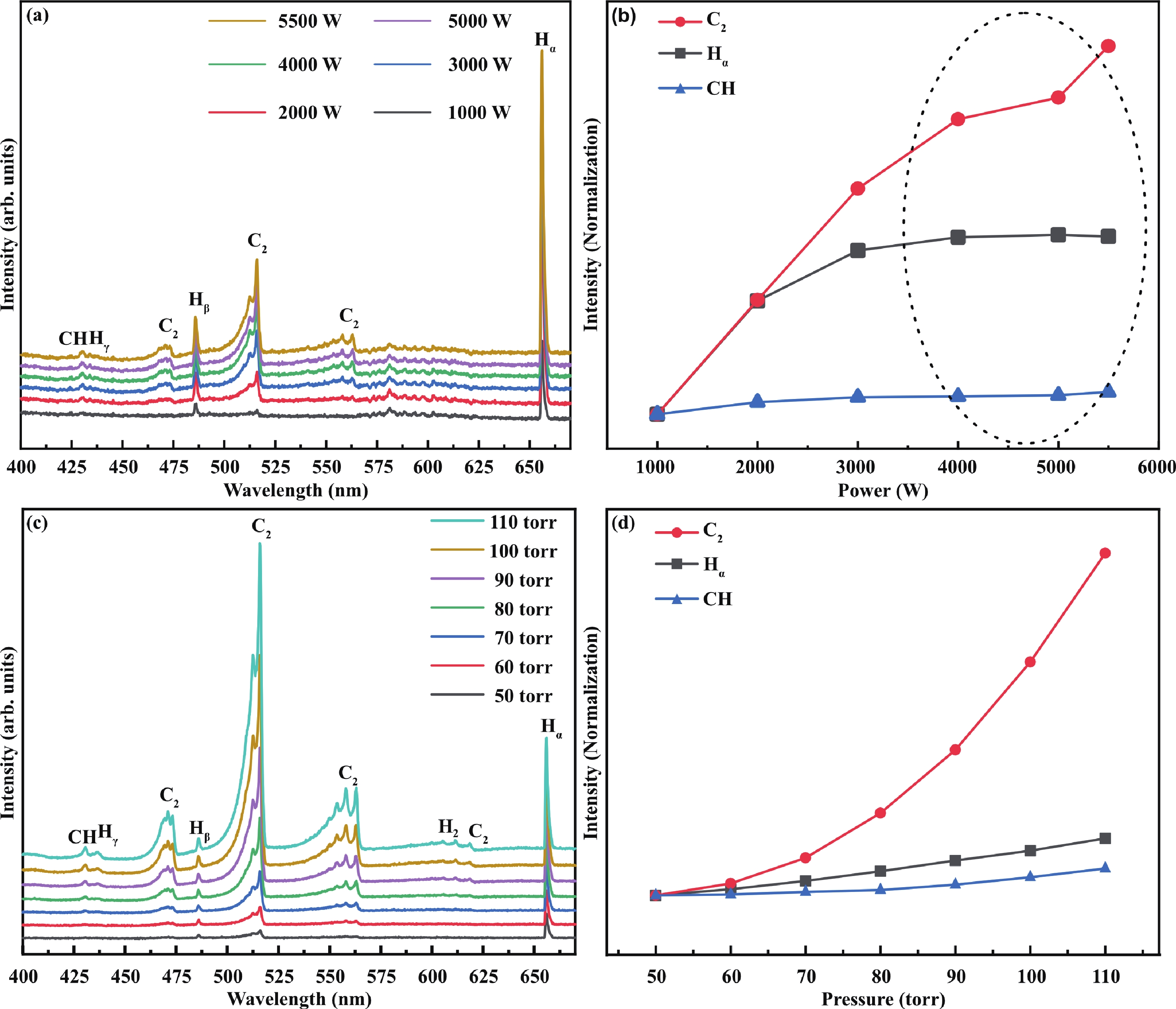
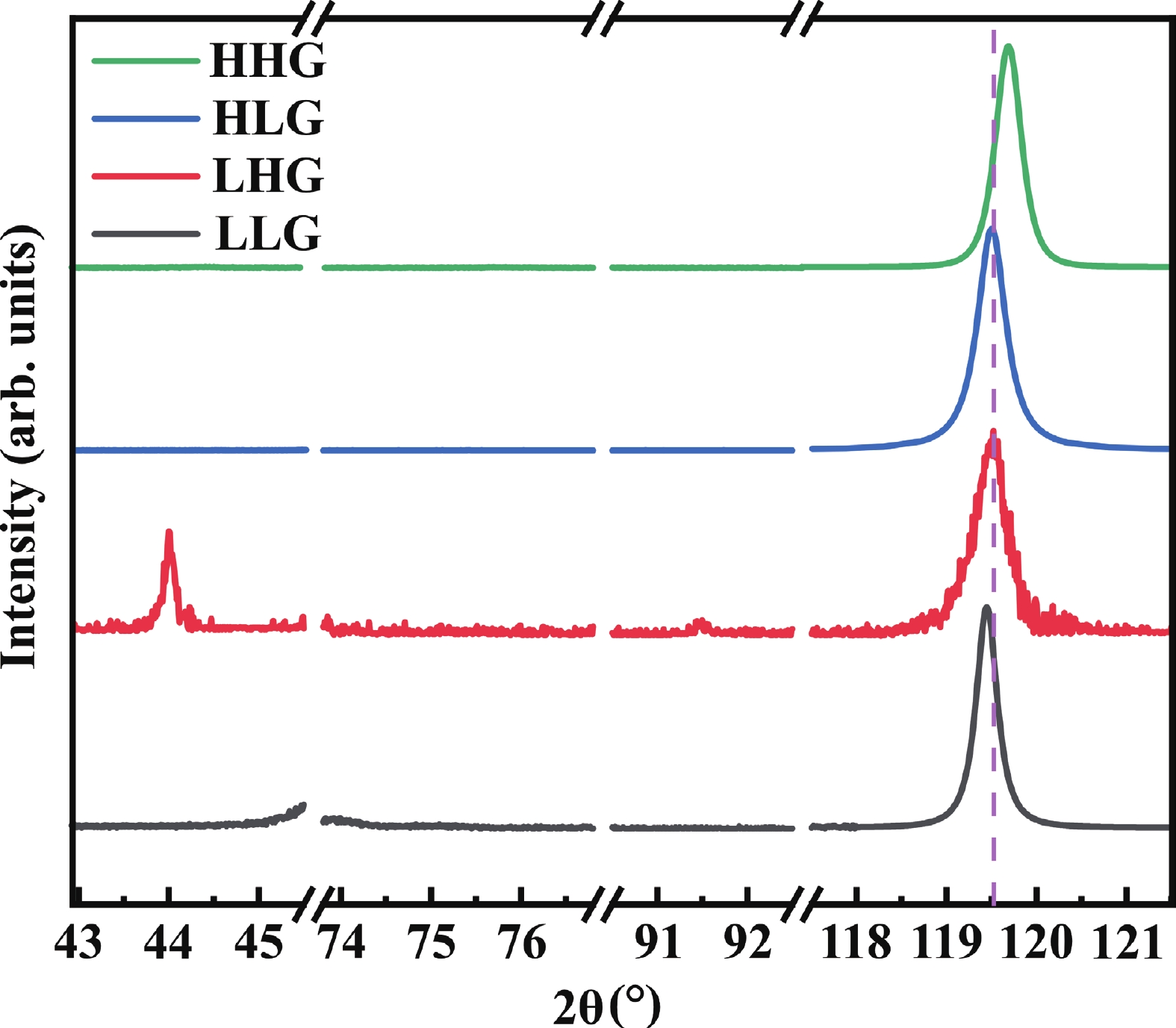
The synthesis of high-quality heteroepitaxial diamond films on iridium composite substrates is a critical step toward advancing diamond for electronic and optical applications. Microwave plasma chemical vapor deposition, combined with in situ optical emission spectroscopy, enables precise control over growth modes through plasma parameter tuning. In this study, we examine how methane concentration, microwave power, and gas pressure influence plasma species and, consequently, the growth modes of heteroepitaxial diamond by optical emission spectroscopy and scanning electron microscope. At low nucleation densities, increased methane concentrations promote the transition from faceted polyhedral to ballas structures, driven by elevated C2 radical concentrations in the plasma. Conversely, at higher nucleation densities, gas pressure, and substrate temperature dominate growth mode determination, leading to diverse morphologies, such as planar, polycrystalline, octahedral, and step-flow growth. These findings elucidate the interplay among plasma species, growth parameters, and growth mode, offering critical insights for optimizing growth conditions and preparing heteroepitaxial diamond films in a specific growth mode.
J. Semicond.
2026, 47(1): 012701 doi: 10.1088/1674-4926/25060013

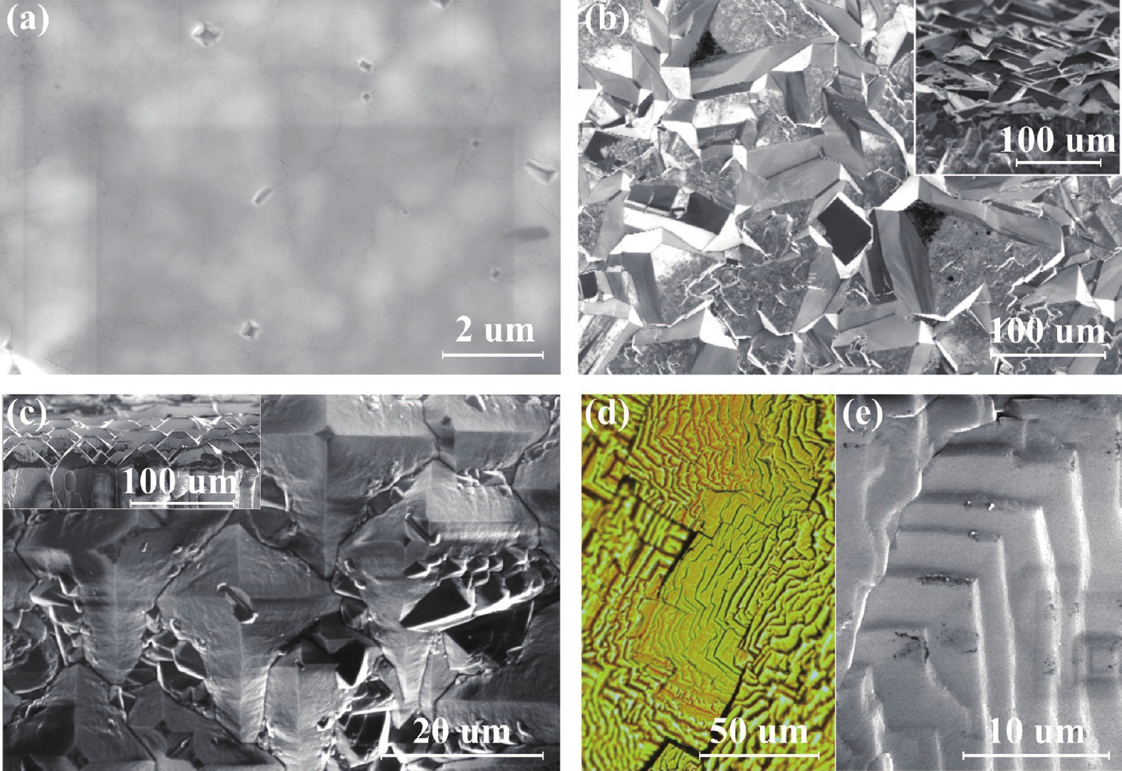
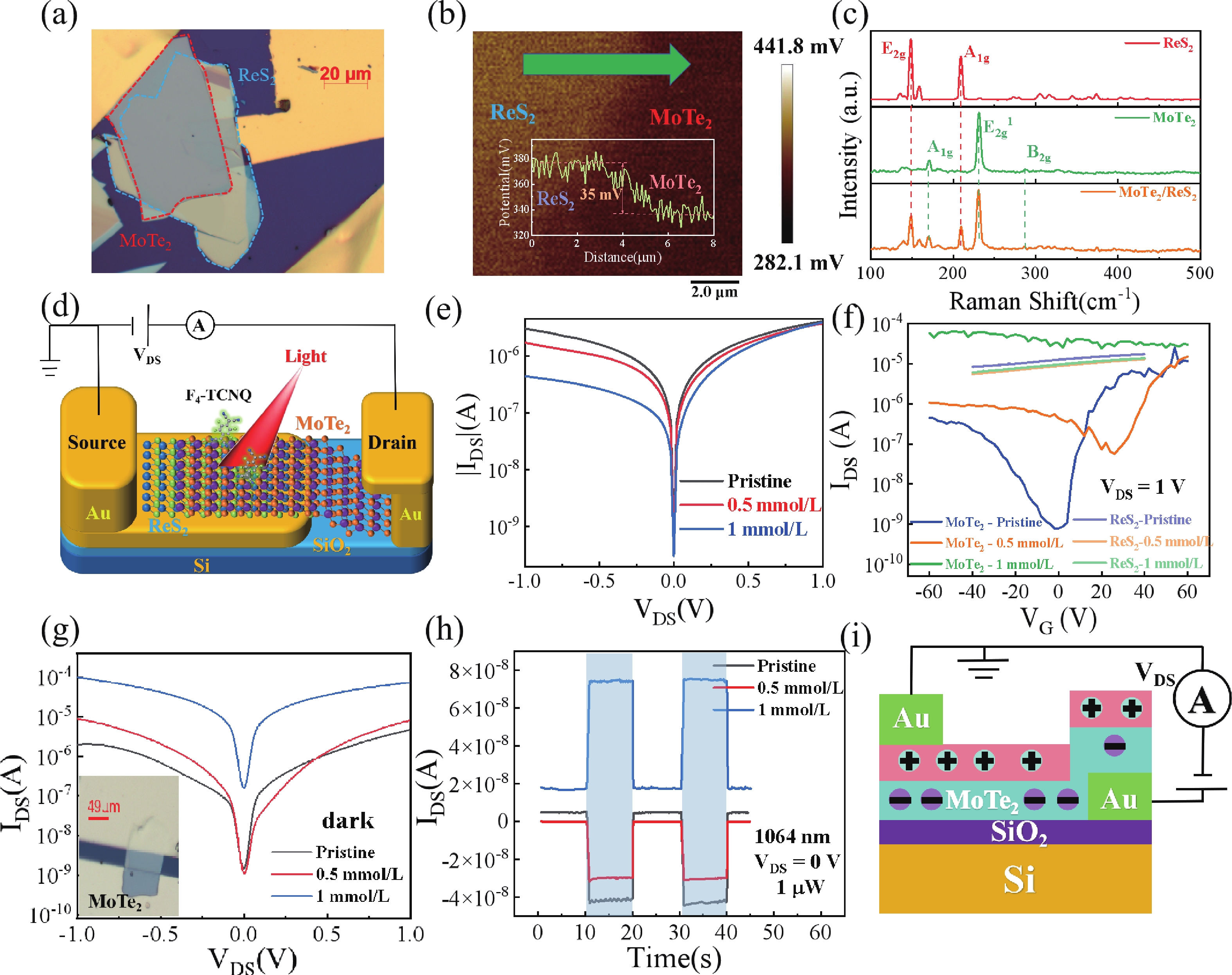
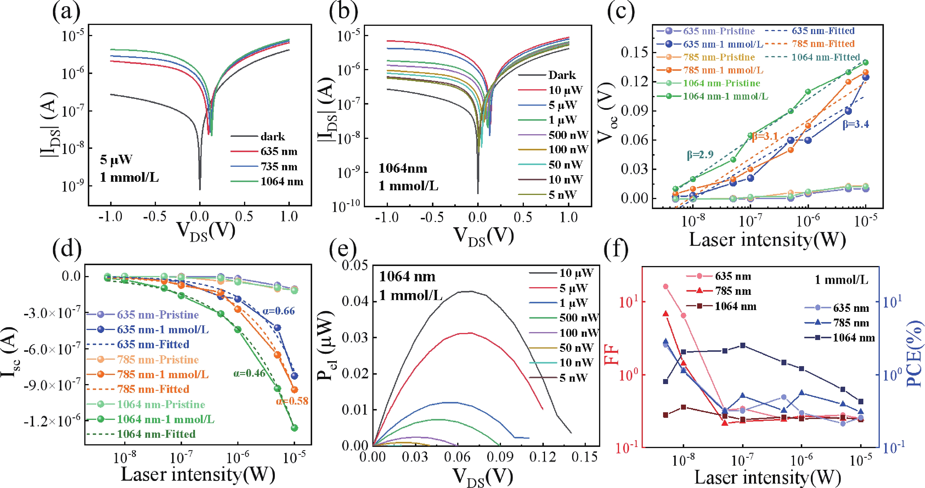
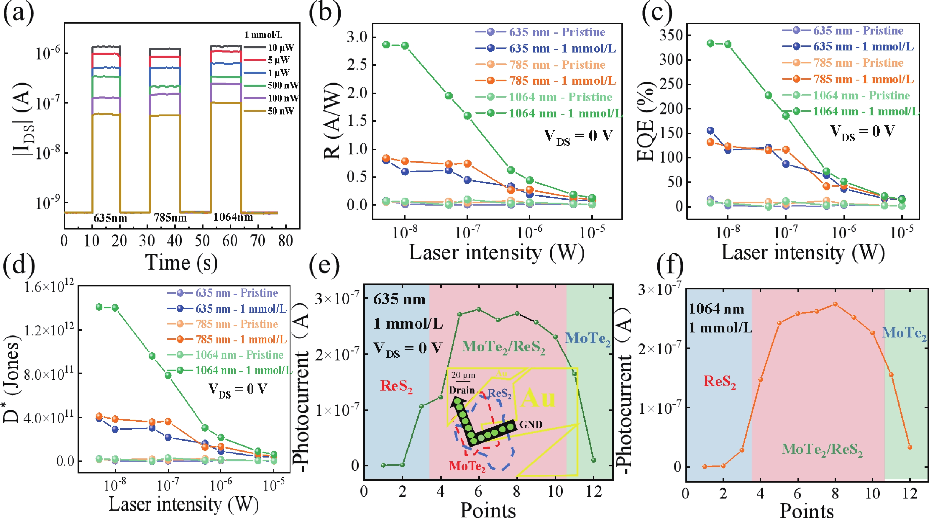
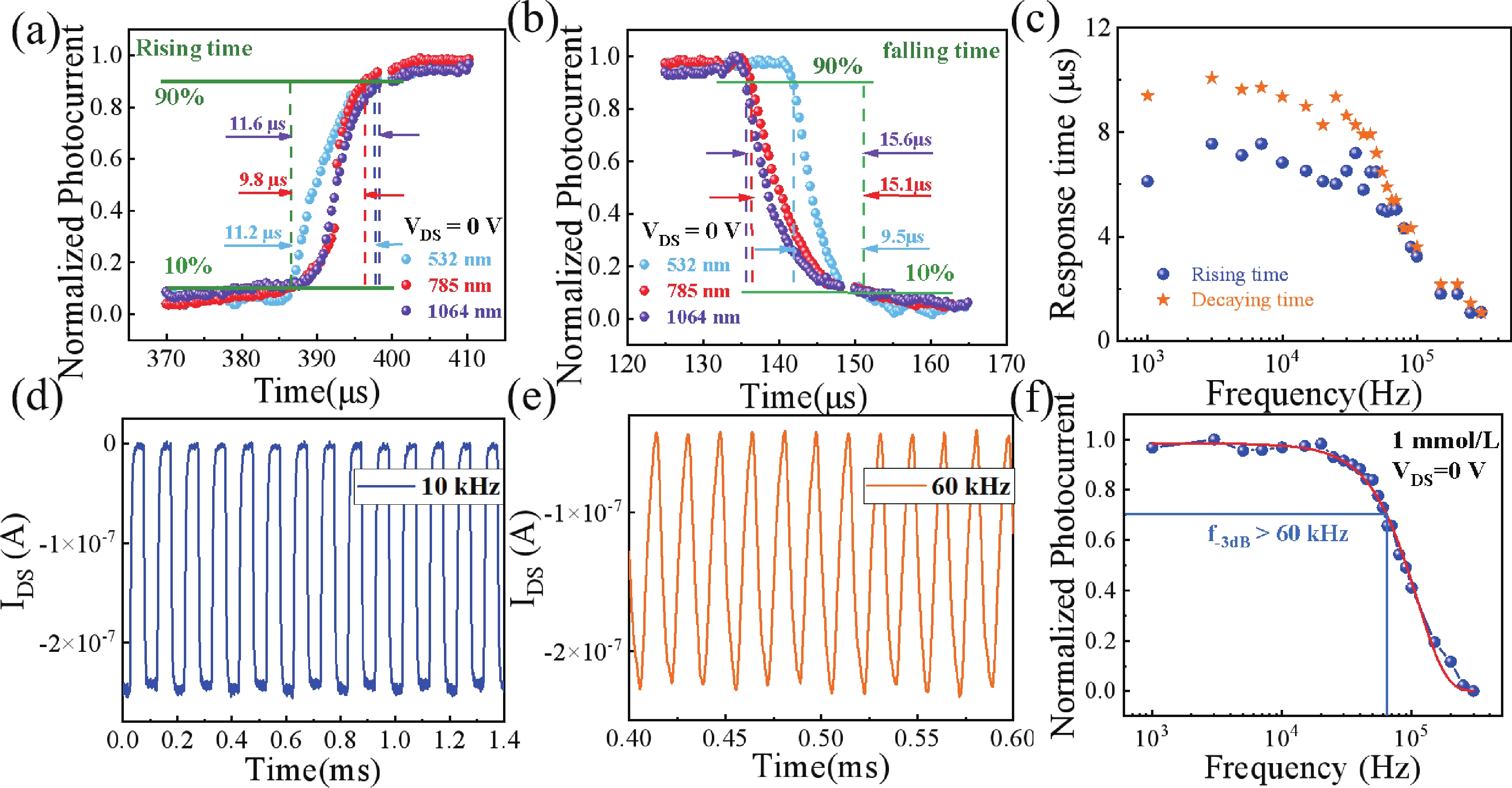
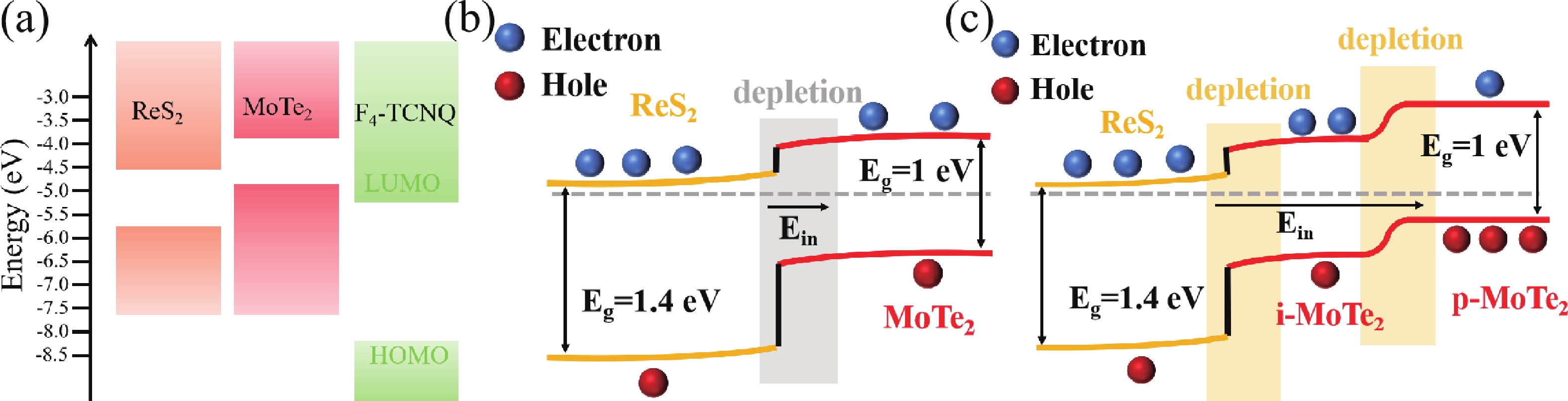
The development of optoelectronic technologies demands photodetectors with miniaturization, broadband operation, high sensitivity, and low power consumption. Although 2D van der Waals (vdW) heterostructures are promising candidates due to their built-in electric fields, ultrafast photocarrier separation, and tunable bandgaps, defect states limit their performance. Therefore, the modulation of the optoelectronic properties in such heterostructures is imperative. Surface charge transfer doping (SCTD) has emerged as a promising strategy for non-destructive modulation of electronic and optoelectronic characteristics in two-dimensional materials. In this work, we demonstrate the construction of high-performance p−i−n vertical heterojunction photodetectors through SCTD of MoTe2/ReS2 heterostructure using p-type F4-TCNQ. Systematic characterization reveals that the interfacial doping process effectively amplifies the built-in electric field, enhancing photogenerated carrier separation efficiency. Compared to the pristine heterojunction device, the doped photodetector exhibits remarkable visible to near-infrared (635−1064 nm) performance. Particularly under 1064 nm illumination at zero bias, the device achieves a responsivity of 2.86 A/W and specific detectivity of 1.41 × 10¹² Jones. Notably, the external quantum efficiency reaches an exceptional value of 334% compared to the initial 11.5%, while maintaining ultrafast response characteristics with rise/fall times of 11.6/15.6 μs. This work provides new insights into interface engineering through molecular doping for developing high-performance vdW optoelectronic devices.
J. Semicond.
2026, 47(1): 012801 doi: 10.1088/1674-4926/25070009
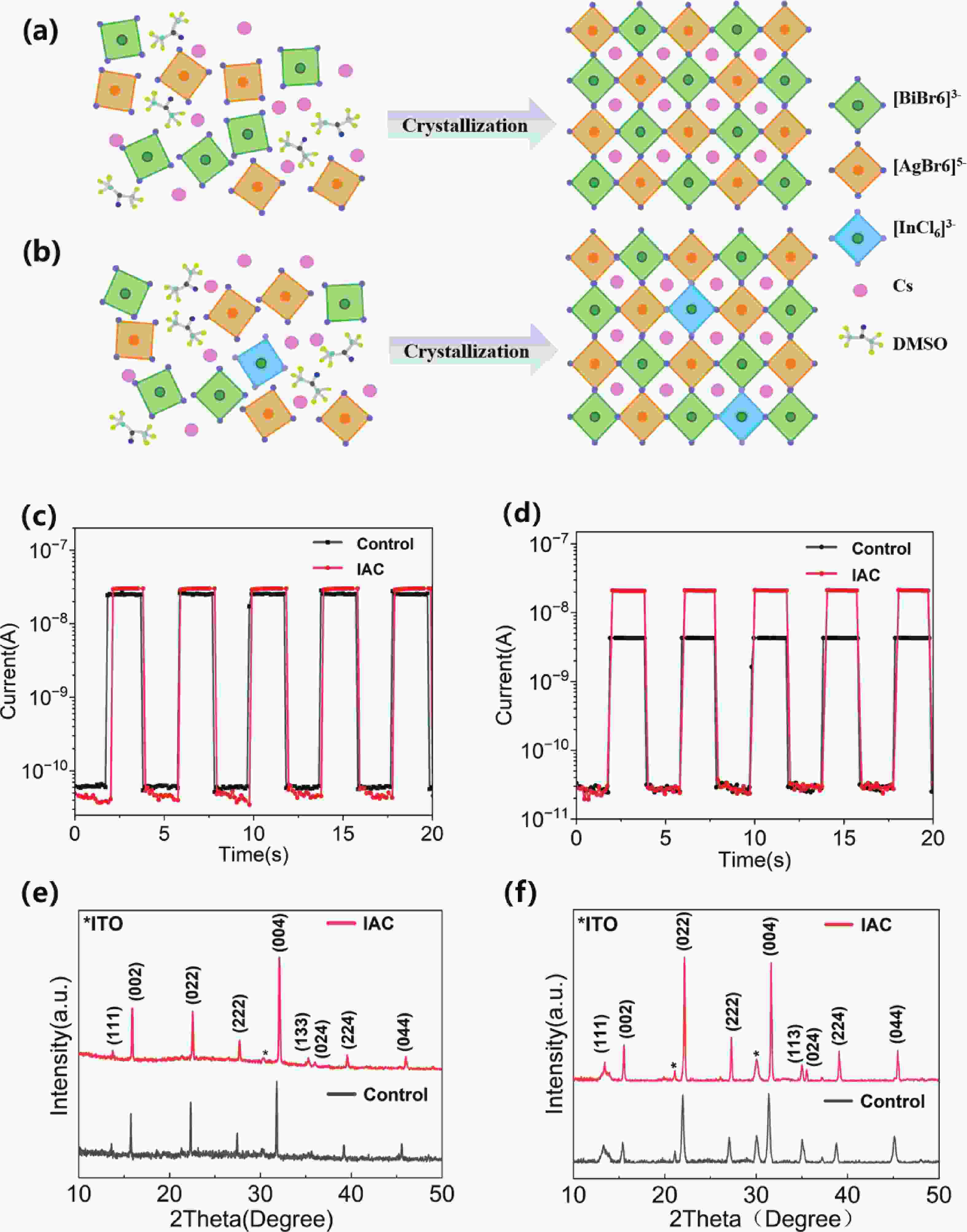
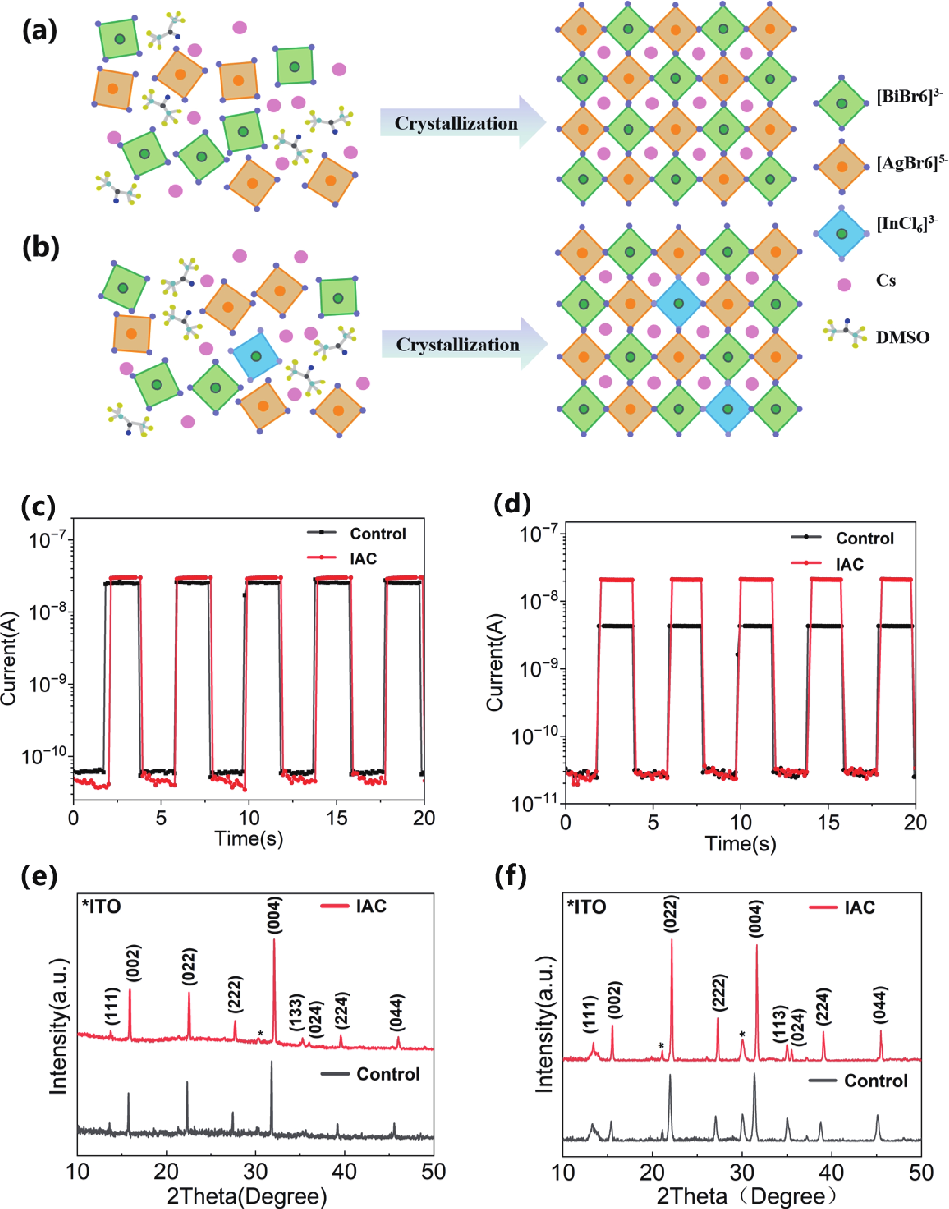
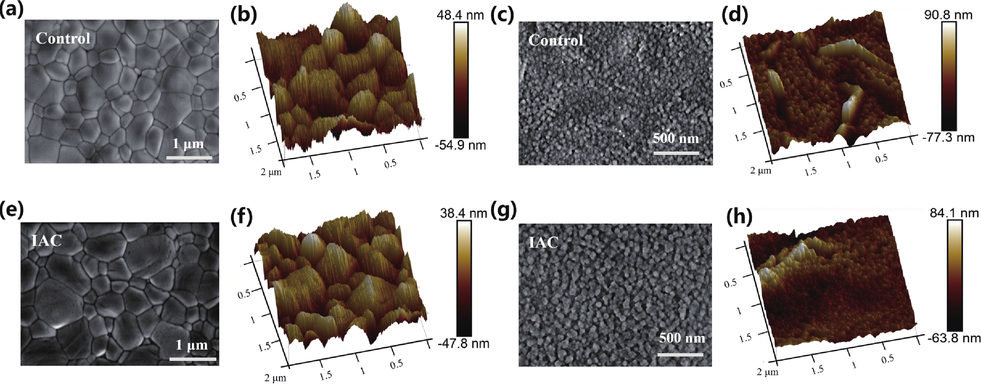
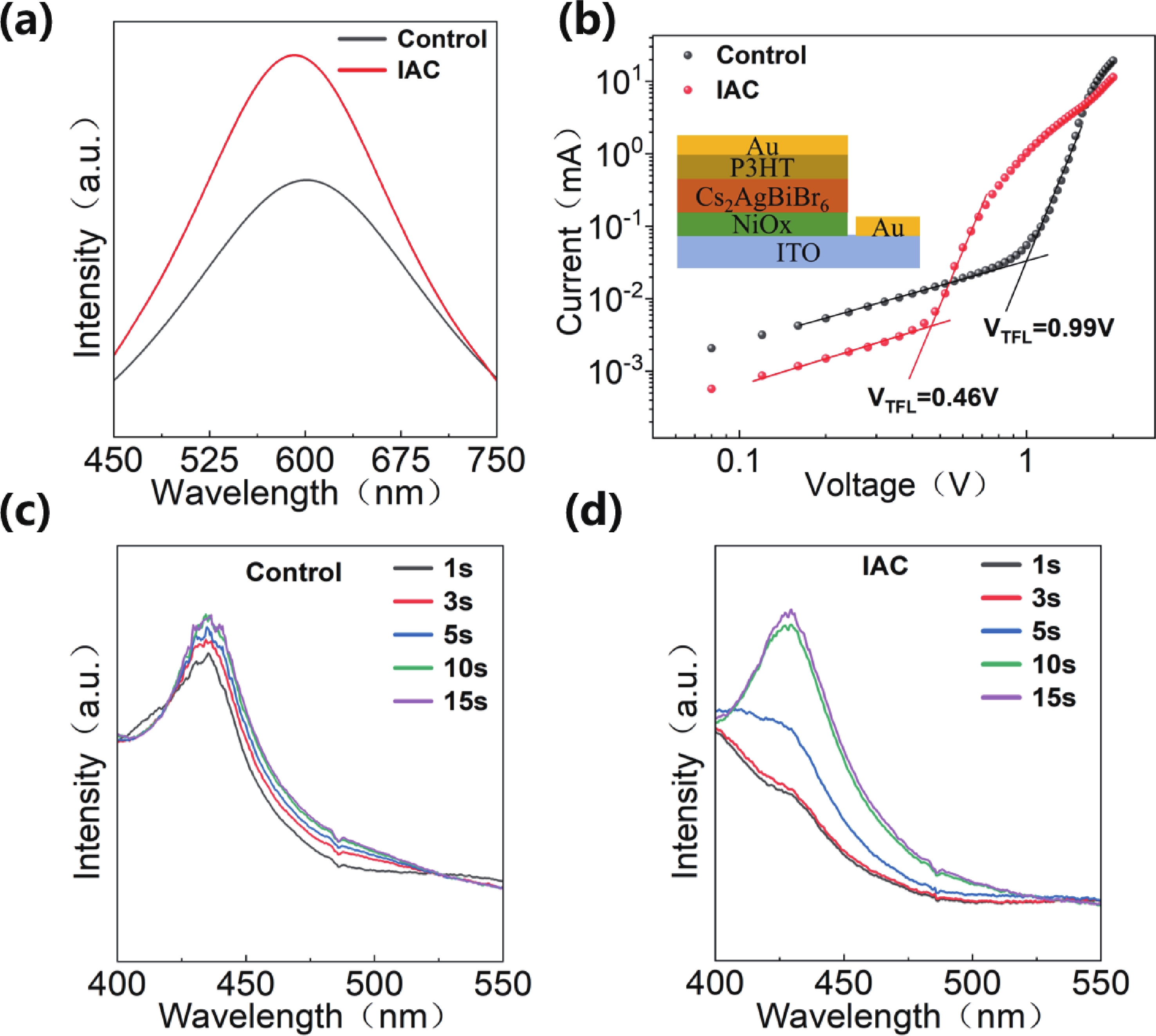
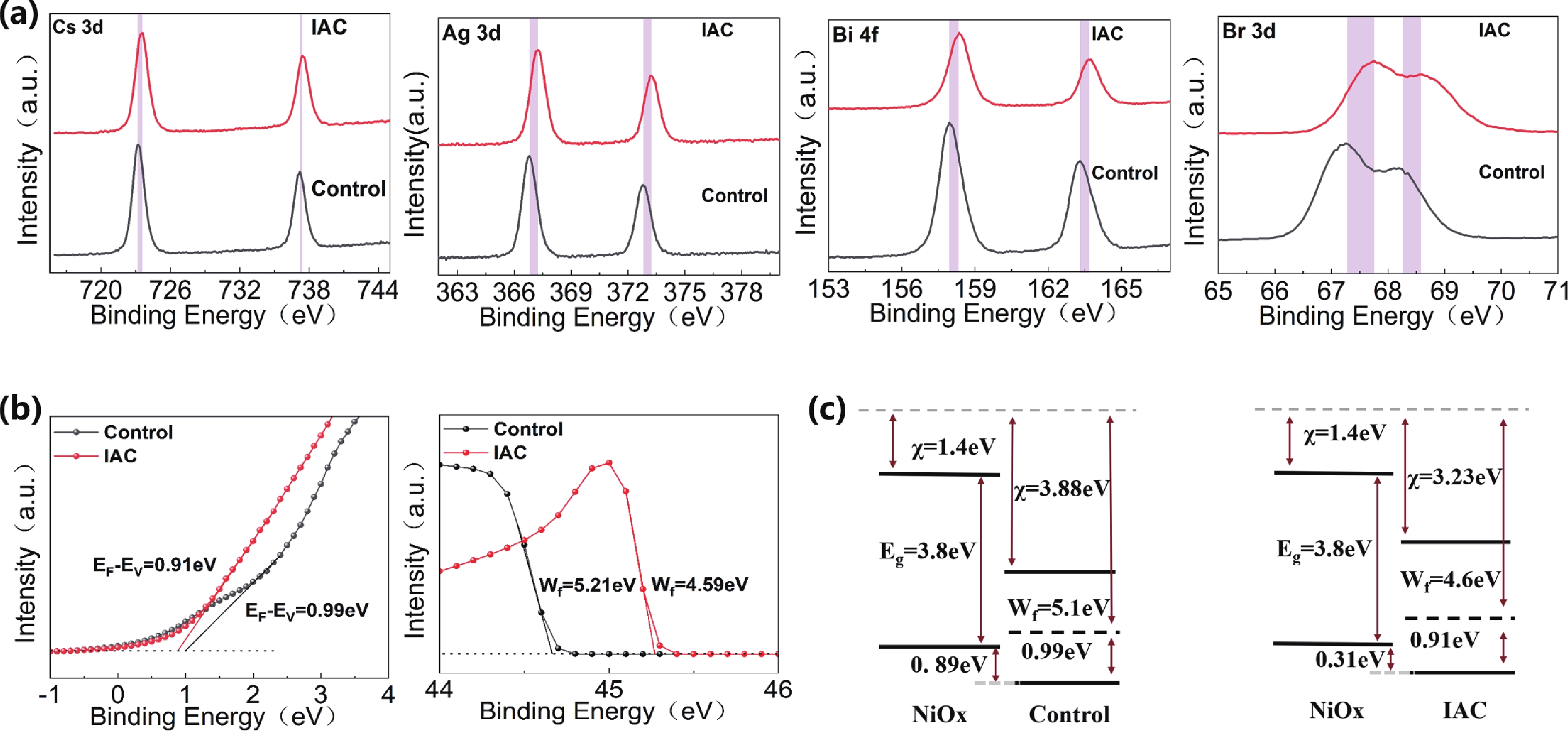
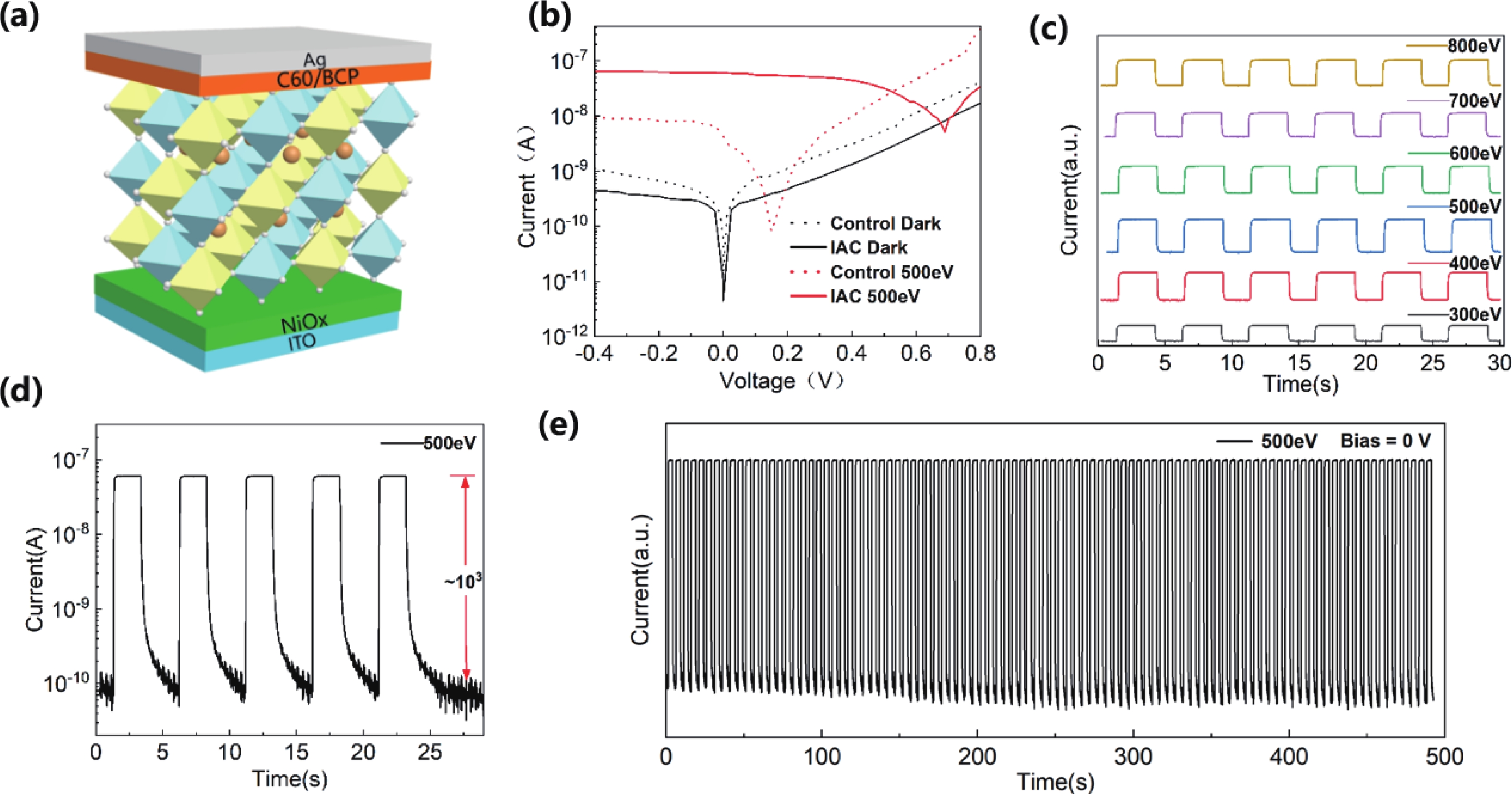
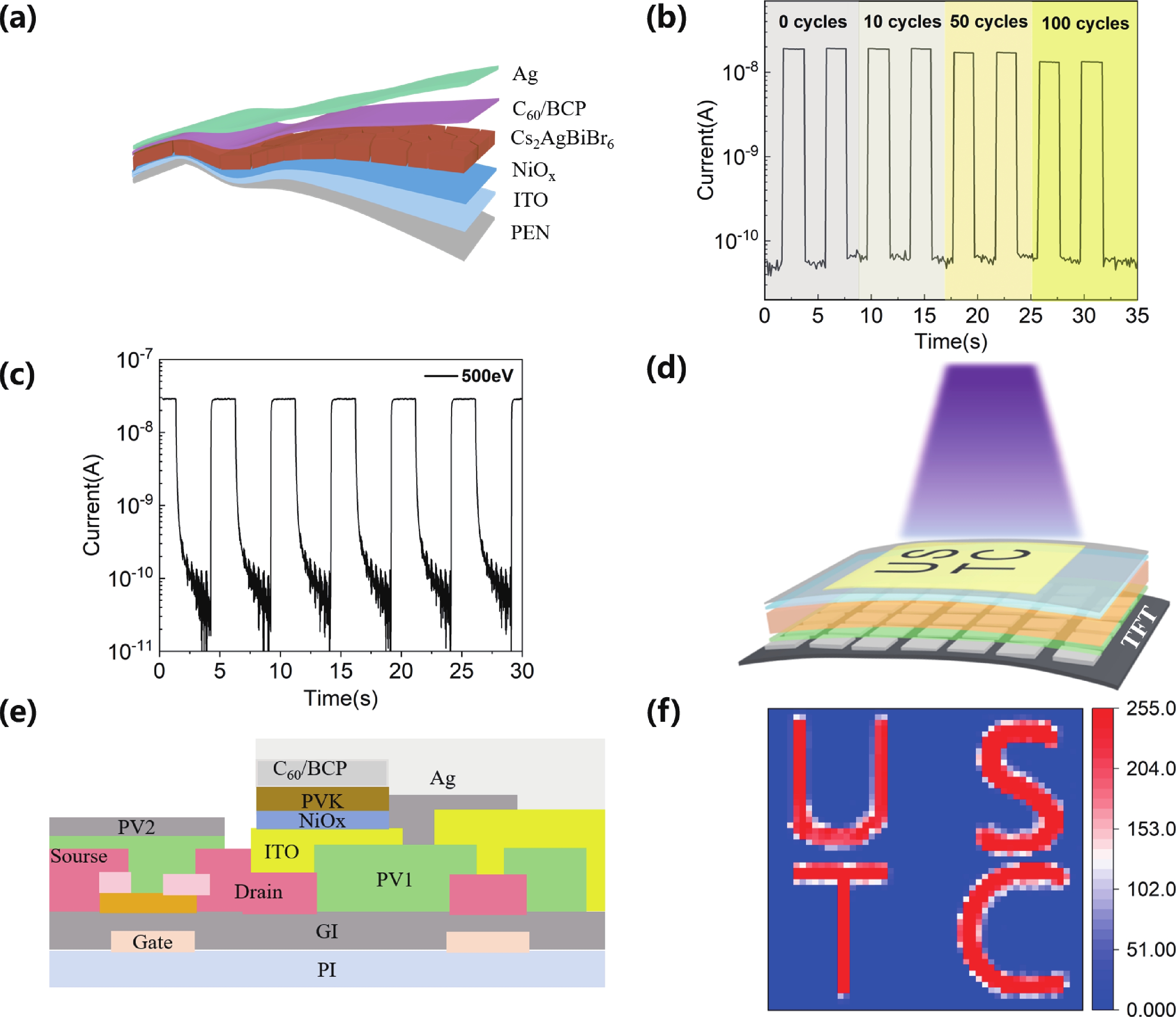
Soft X-ray detectors play a vital role in materials science, high-energy physics and medical imaging. Cs2AgBiBr6, a lead-free double perovskite, has gained attention for its excellent optoelectronic properties, stability, and nontoxicity. However, its fast crystallization and requirement for high-temperature annealing (>250 °C) often lead to inferior film quality, limiting its application in flexible devices. This study introduces an alloying strategy that significantly improves the quality of Cs2AgBiBr6 thin films annealed at a reduced temperature of 150 °C. Devices based on the alloyed thin films exhibit an ultra-low dark current of 0.32 nA∙cm−2 and a quantum efficiency of 725%. Furthermore, the first successful integration of Cs2AgBiBr6 with a thin-film transistor backplane demonstrates its superior imaging performance, indicating that Cs2AgBiBr6 is a promising material for next-generation soft X-ray sensors.
J. Semicond.
2026, 47(1): 012802 doi: 10.1088/1674-4926/25090001
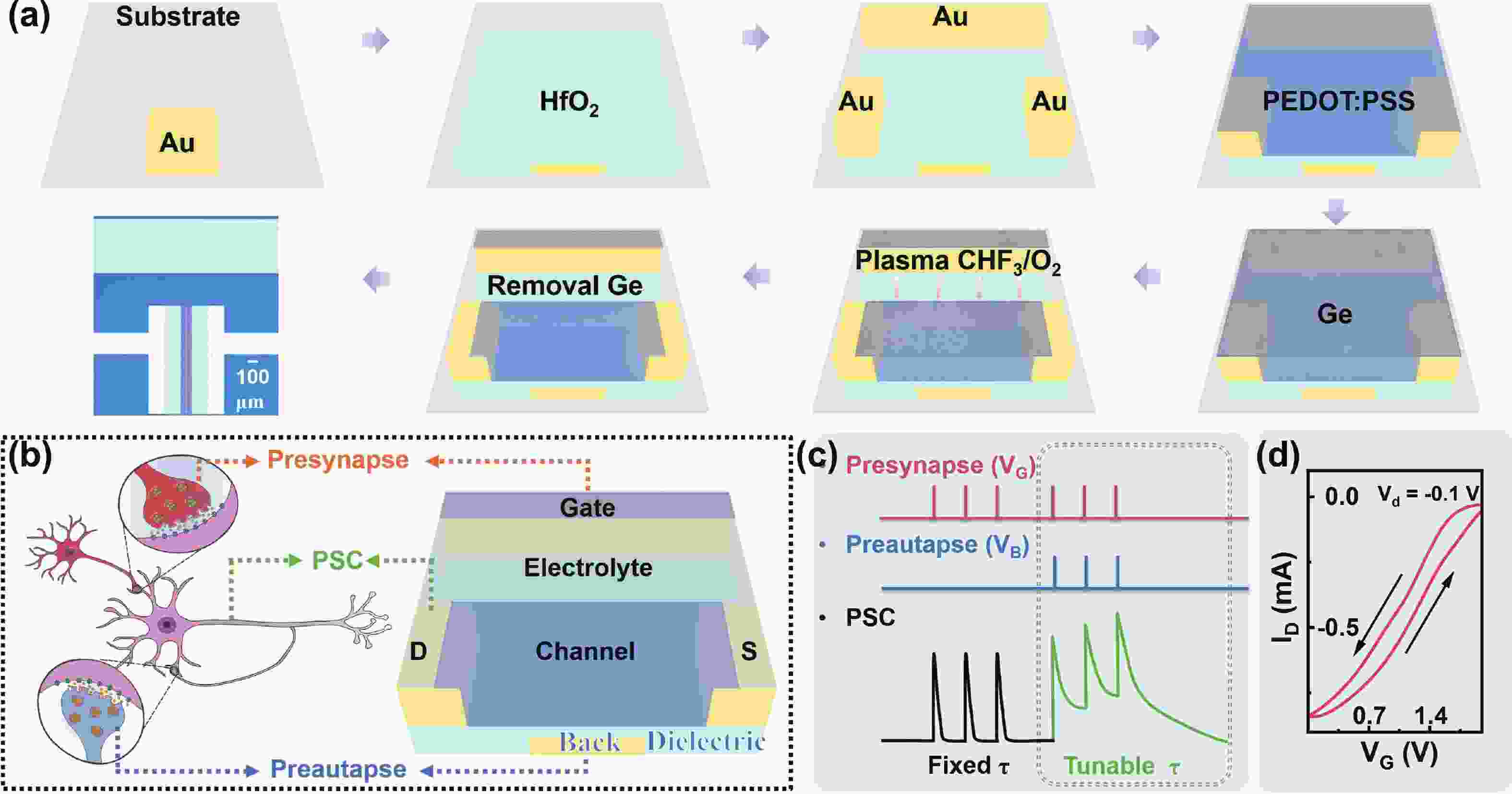
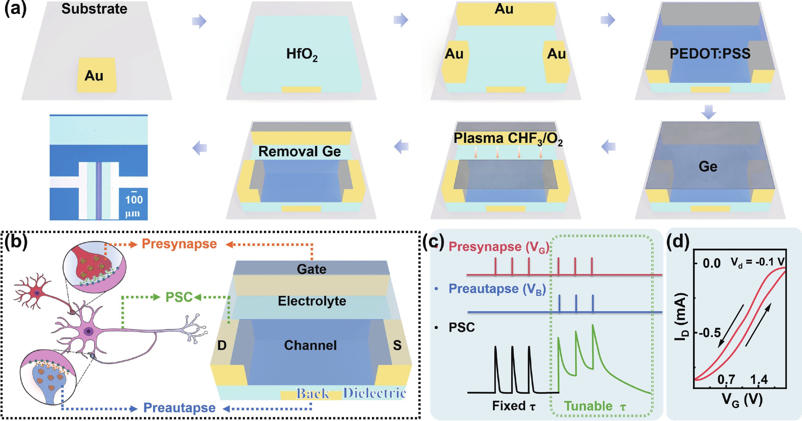
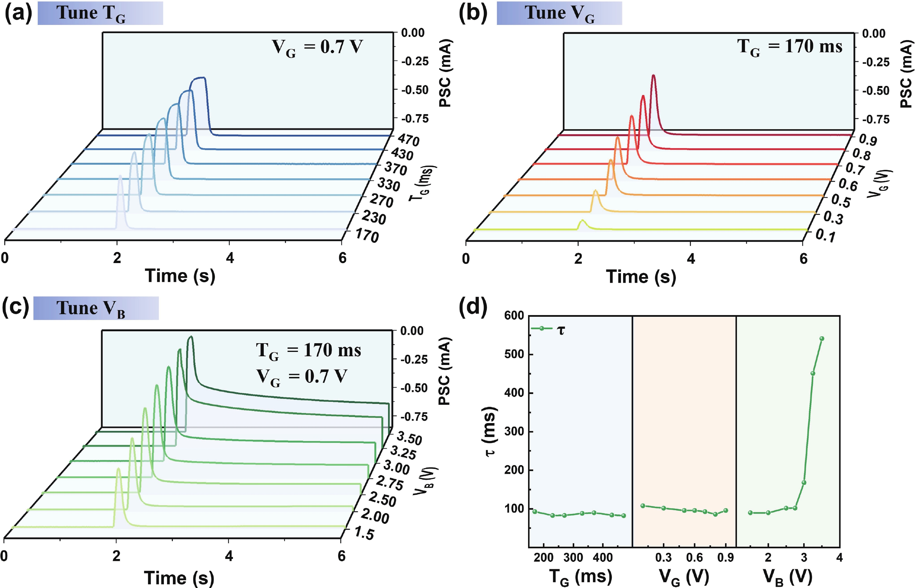
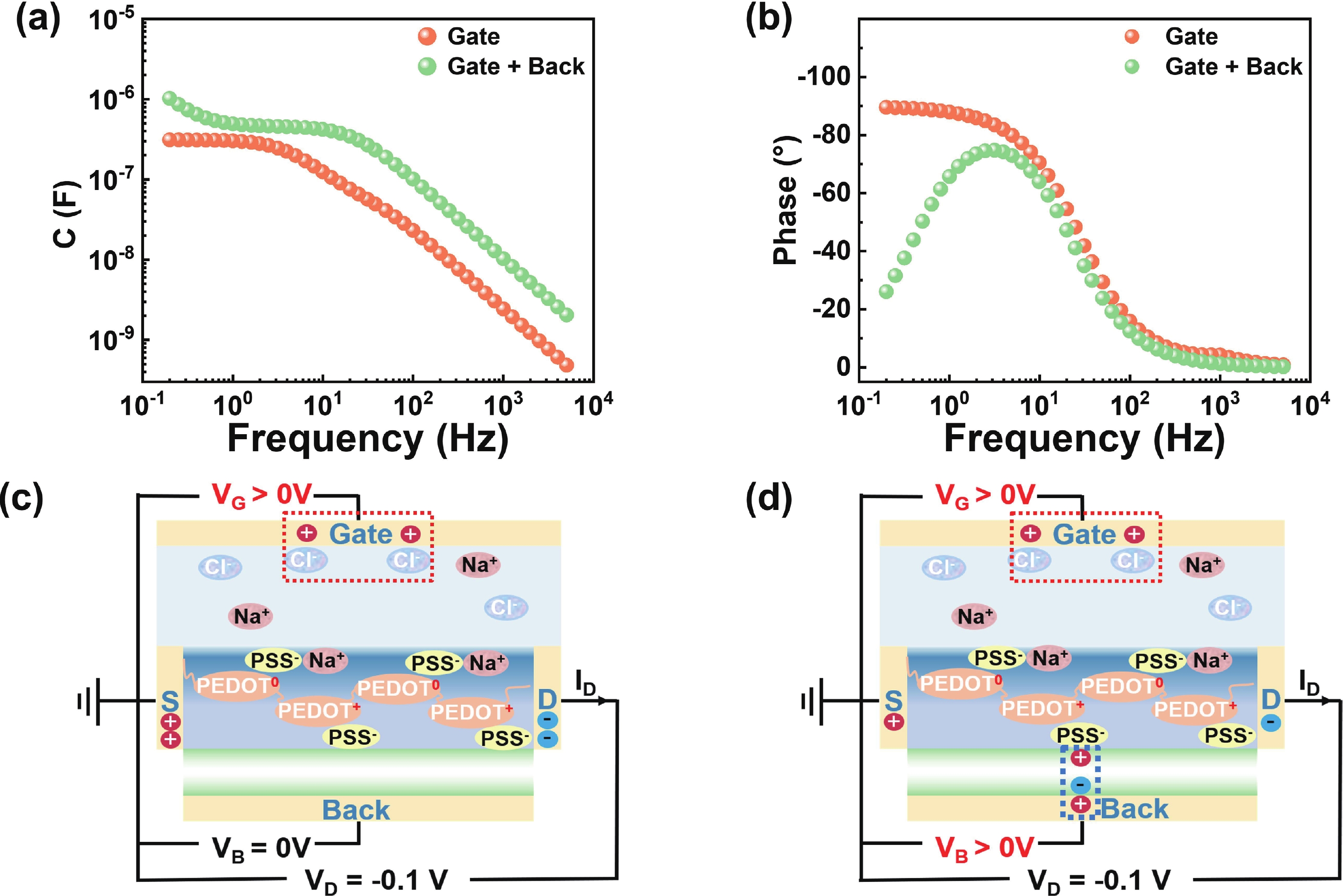
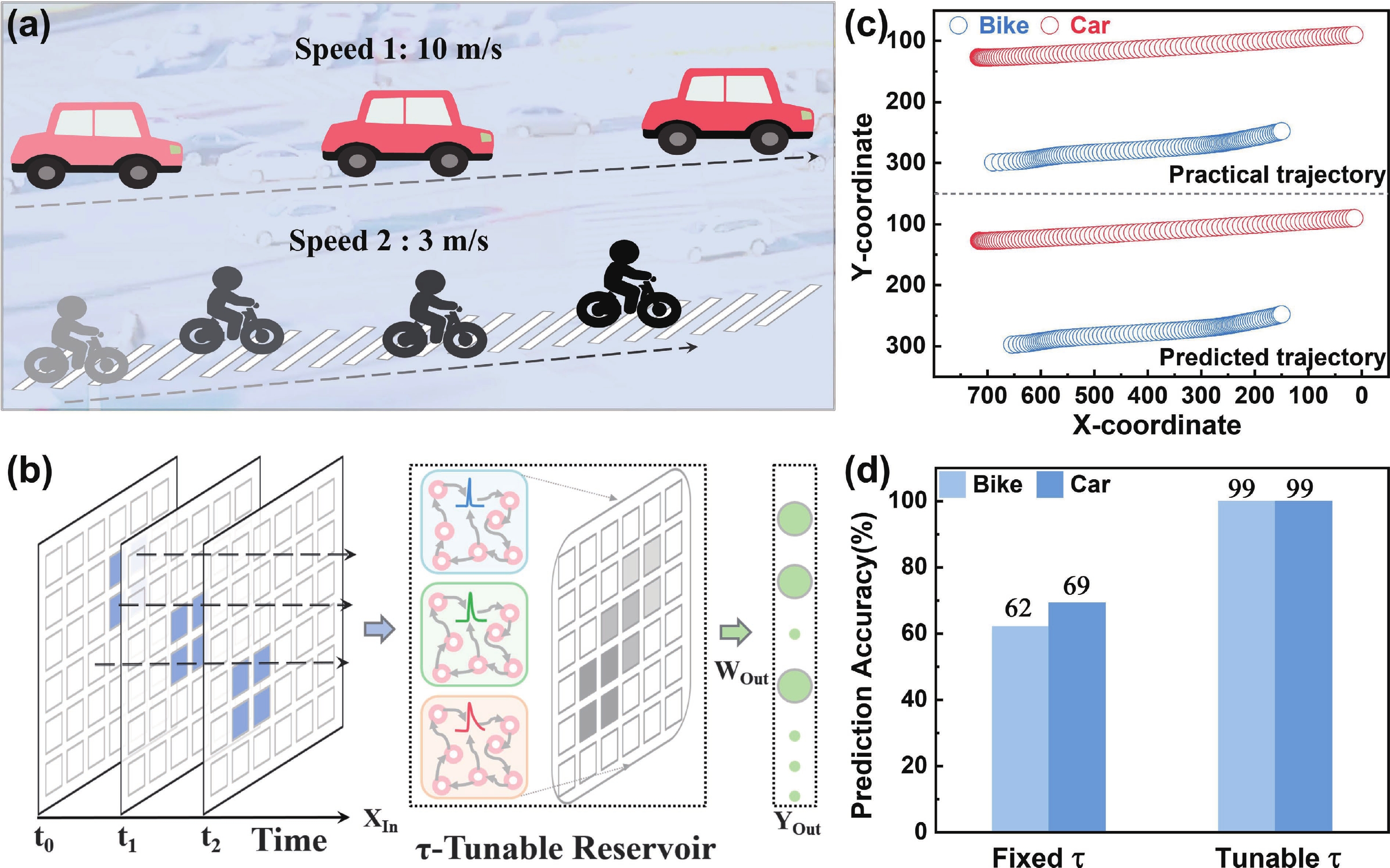
Organic electrochemical transistor (OECT) devices demonstrate great promising potential for reservoir computing (RC) systems, but their lack of tunable dynamic characteristics limits their application in multi-temporal scale tasks. In this study, we report an OECT-based neuromorphic device with tunable relaxation time (τ) by introducing an additional vertical back-gate electrode into a planar structure. The dual-gate design enables τ reconfiguration from 93 to 541 ms. The tunable relaxation behaviors can be attributed to the combined effects of planar-gate induced electrochemical doping and back-gate-induced electrostatic coupling, as verified by electrochemical impedance spectroscopy analysis. Furthermore, we used the τ-tunable OECT devices as physical reservoirs in the RC system for intelligent driving trajectory prediction, achieving a significant improvement in prediction accuracy from below 69% to 99%. The results demonstrate that the τ-tunable OECT shows a promising candidate for multi-temporal scale neuromorphic computing applications.