Significant progress has been achieved in the field of organic solar cells (OSCs). Most devices with power conversion efficiencies (PCEs) exceeding 20% rely predominantly on active materials that incorporate D18 or its derivatives as the donor. In contrast, the PCEs over 20% have been realized as well for OSCs with the non-D18-based donor materials by simultaneously optimizing material properties, active layer morphologies and interface engineering, thereby demonstrating the potential to outperform D18 counterparts. Therefore, this review summarizes an overview of recent advancements in OSCs with the PCEs over 20% utilizing the non-D18-based donor materials, and highlights three critical aspects including molecular design strategies, the active layer morphologies, and the interface optimization. Their synergistic roles are advantageous in enhancing the exciton dissociation, facilitating the charge transport, and suppressing the recombination losses, accordingly supporting the improved PCEs over 20%. Furthermore, the challenges and valuable insights are discussed, which can lead to improved efficiency, scalable fabrication, and enhanced environmental and thermal stability, potentially accelerating the commercialization of OSCs.


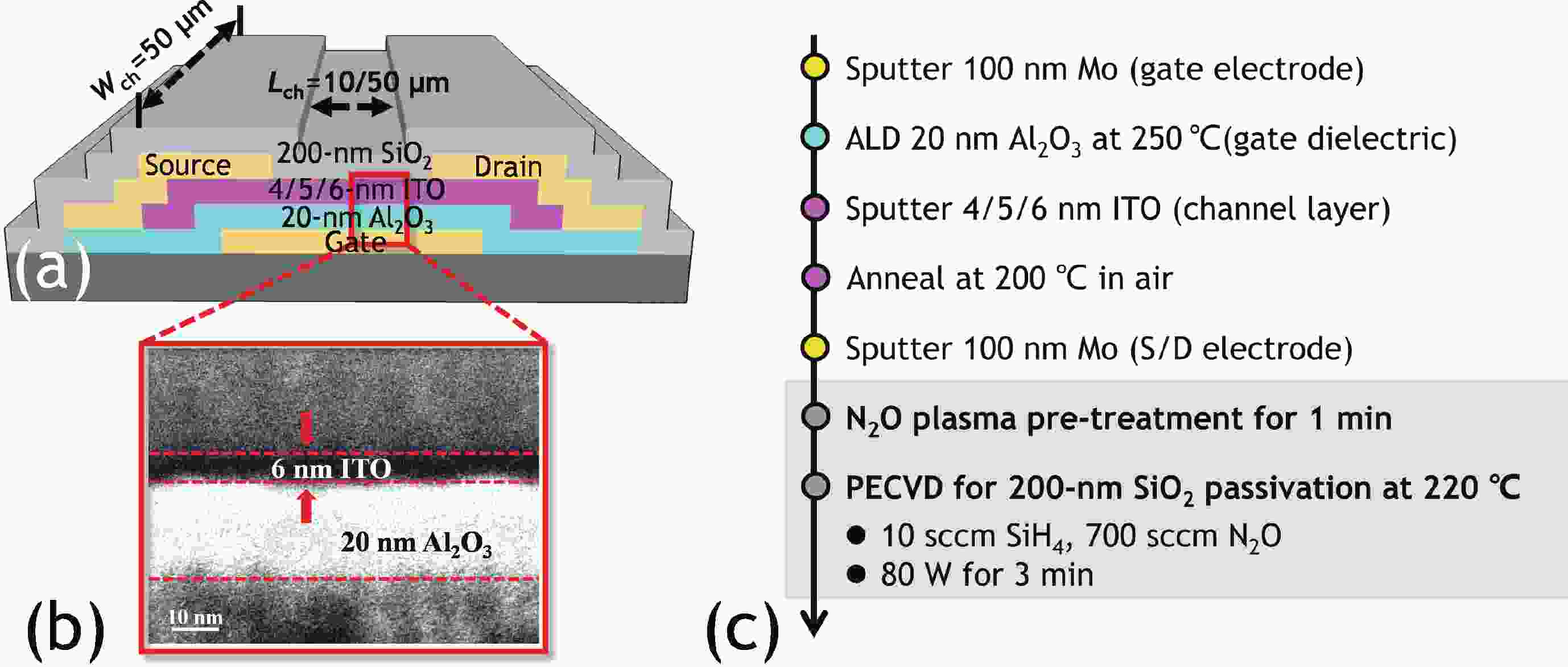
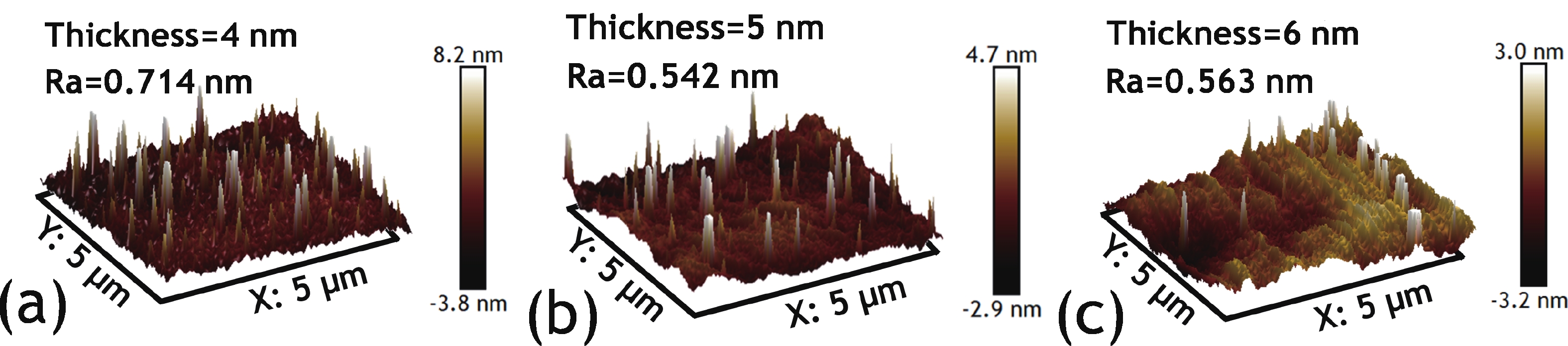
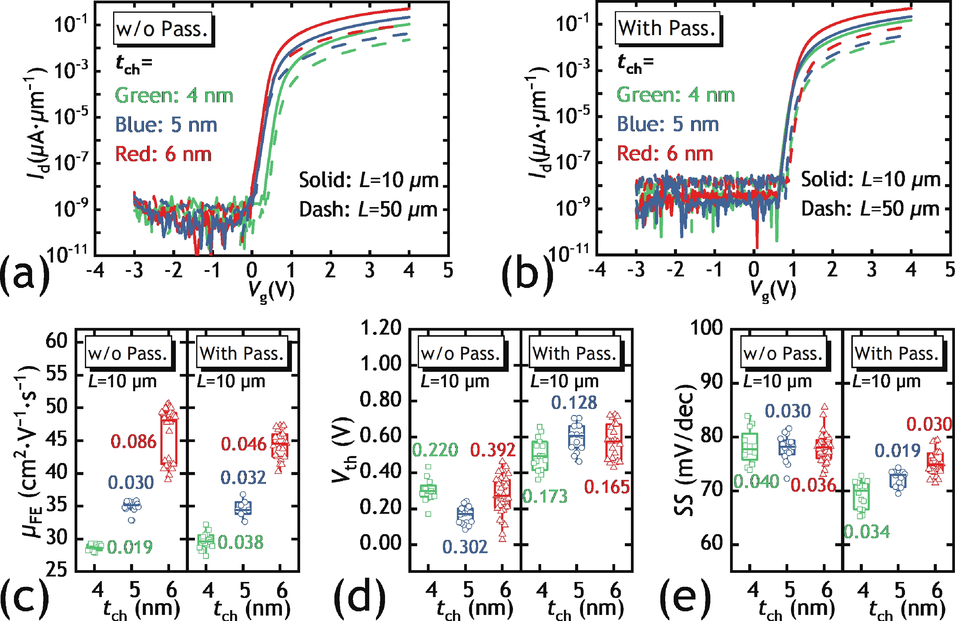
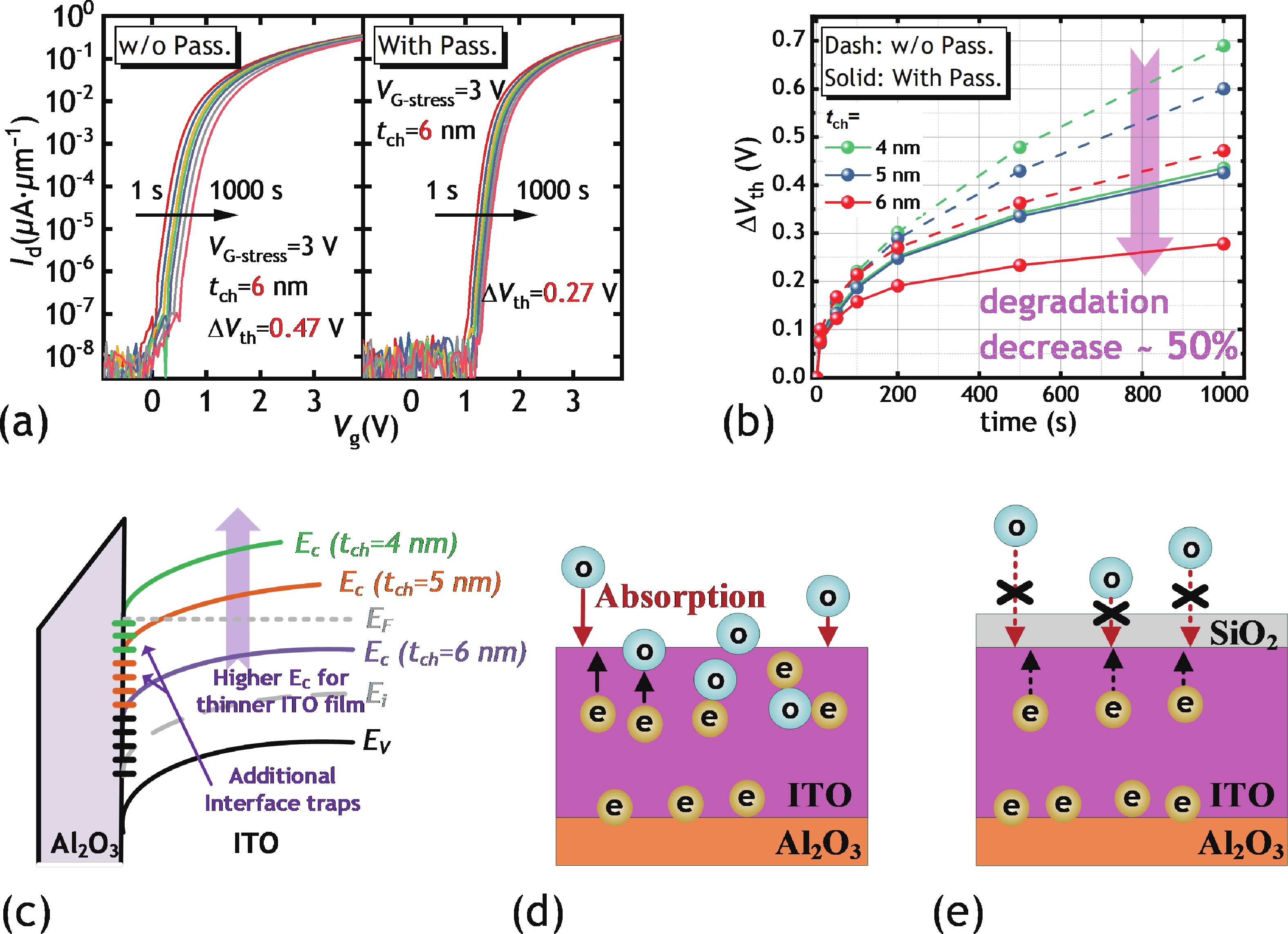
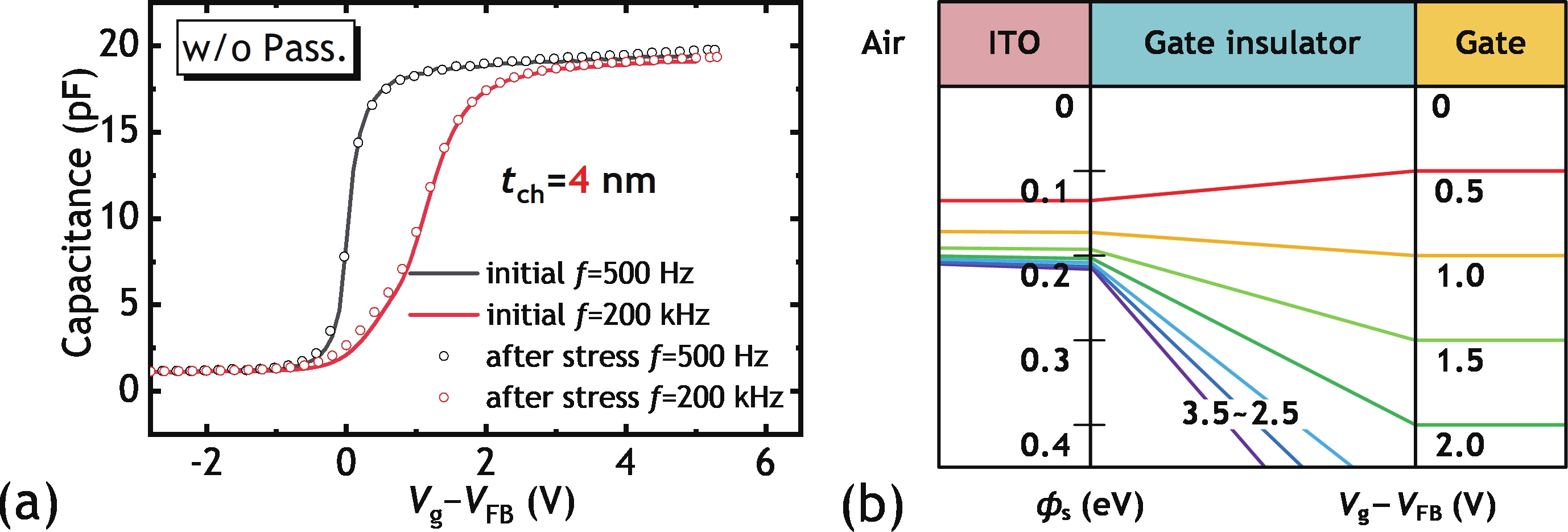
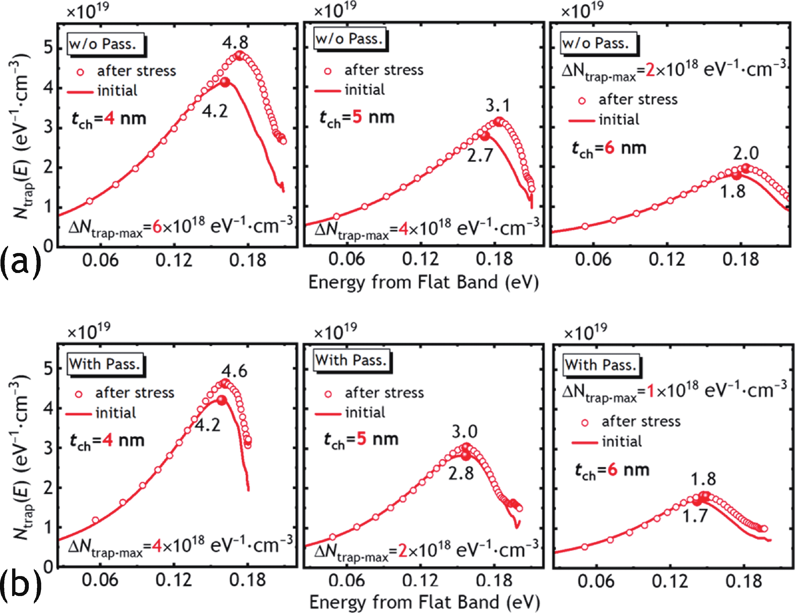
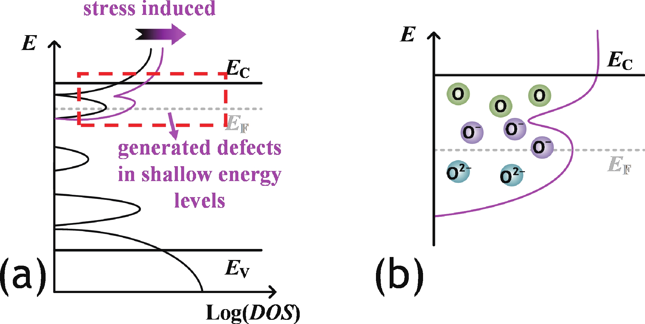
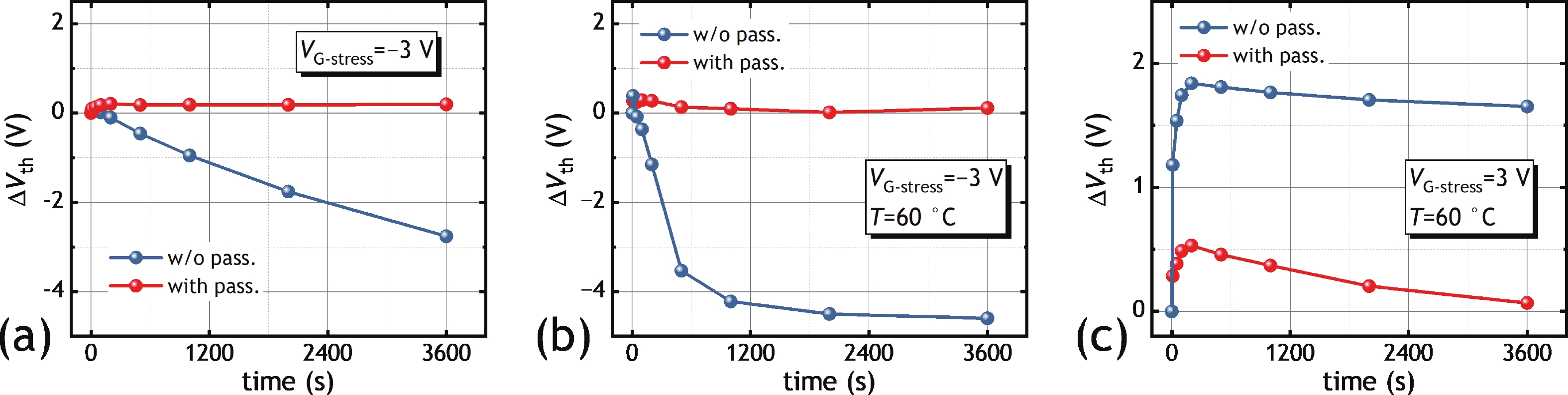
In this work, we demonstrated the InSnO (ITO) TFTs passivated with SiO2 via the PECVD process compatible with large-area production for the first time. The passivated ITO TFTs with various channel thicknesses (tch = 4, 5, 6 nm) exhibit excellent electrical performance and superior uniformity. The reliability properties of ITO TFTs were evaluated in detail under positive bias stress (PBS) conditions before and after passivation. Compared to the devices without passivation, the passivated devices have only 50% threshold voltage degradation (ΔVth) and 50% newly generated traps due to excellent isolation of the ambient atmosphere. The negligible performance degradation of ITO TFTs with passivation during negative bias stress (NBS) and negative bias temperature stress (NBTS) verifies the outstanding immunity to the water vapor of the SiO2 passivation layer. Overall, the ITO TFT with the tch of 6 nm and with SiO2 passivation exhibits the best performance in terms of electrical properties, uniformity, and reliability, which is promising in large-area production.
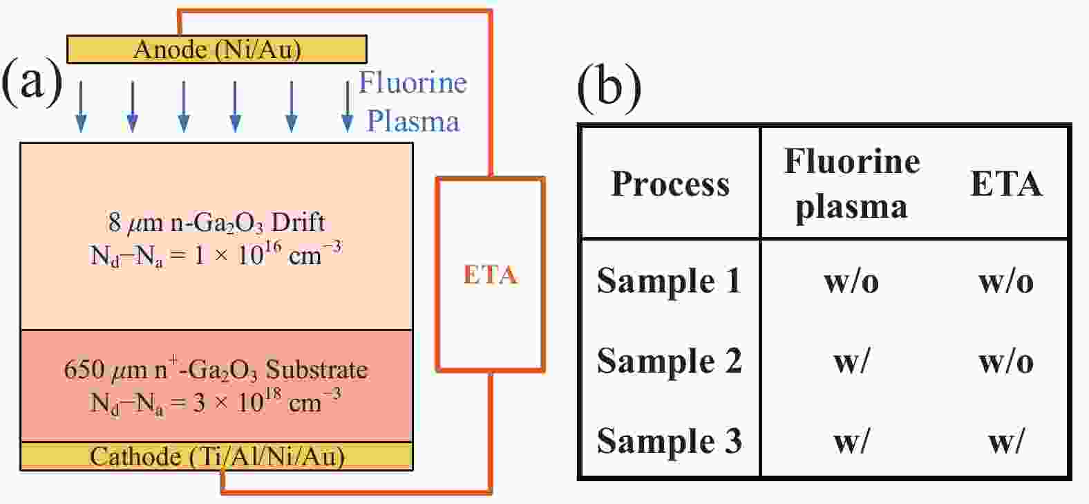
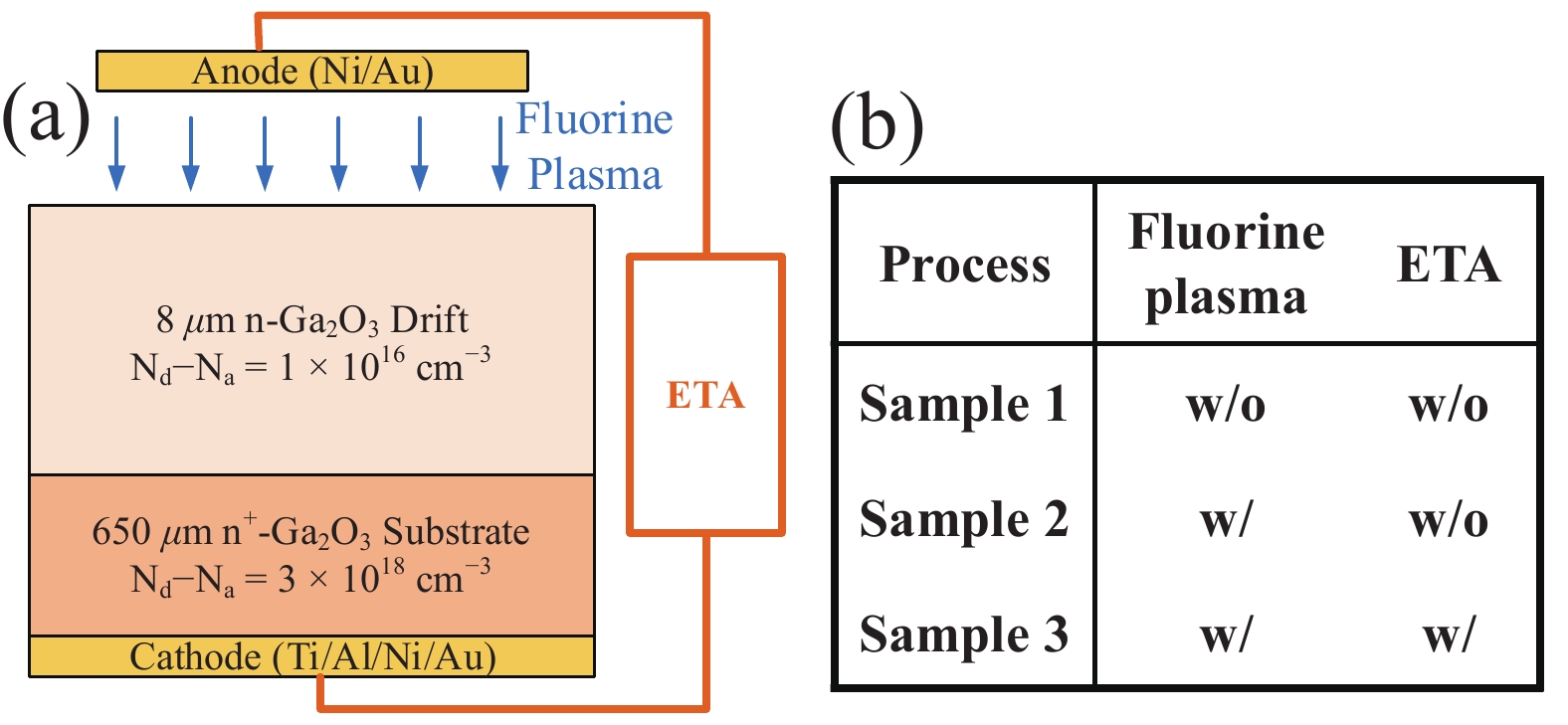
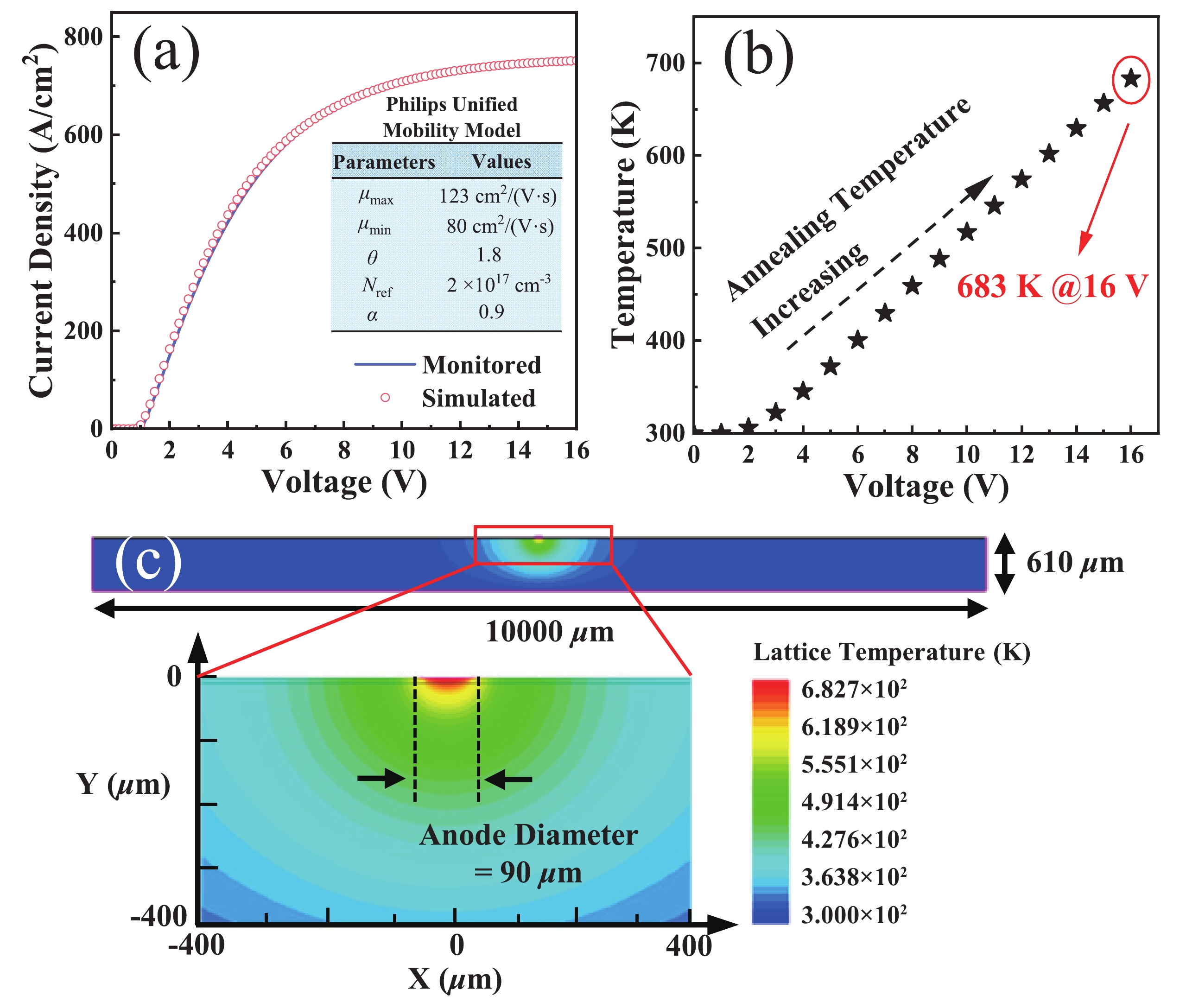
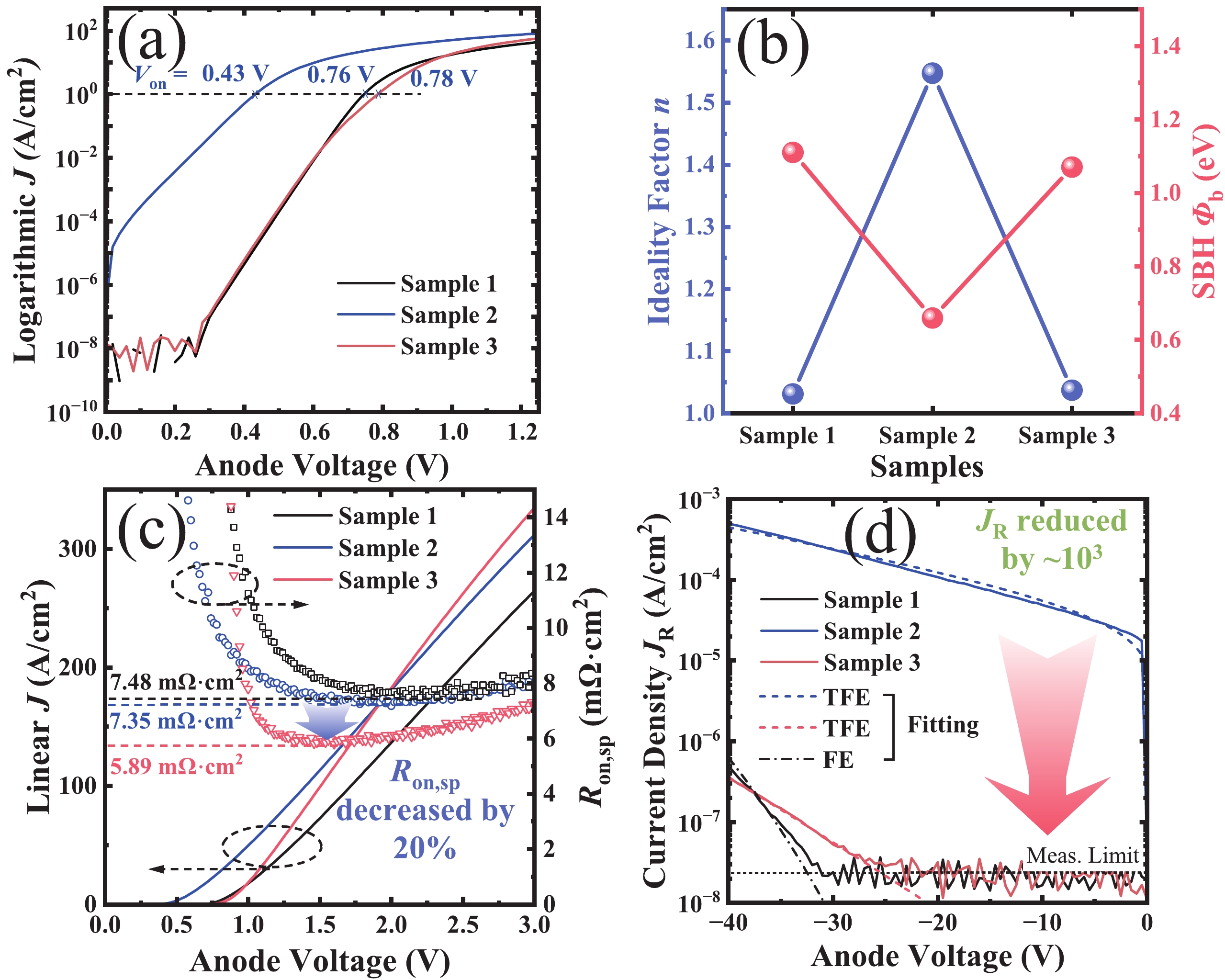
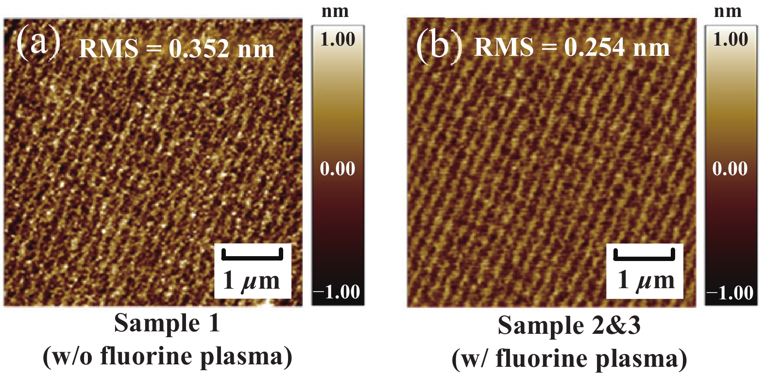
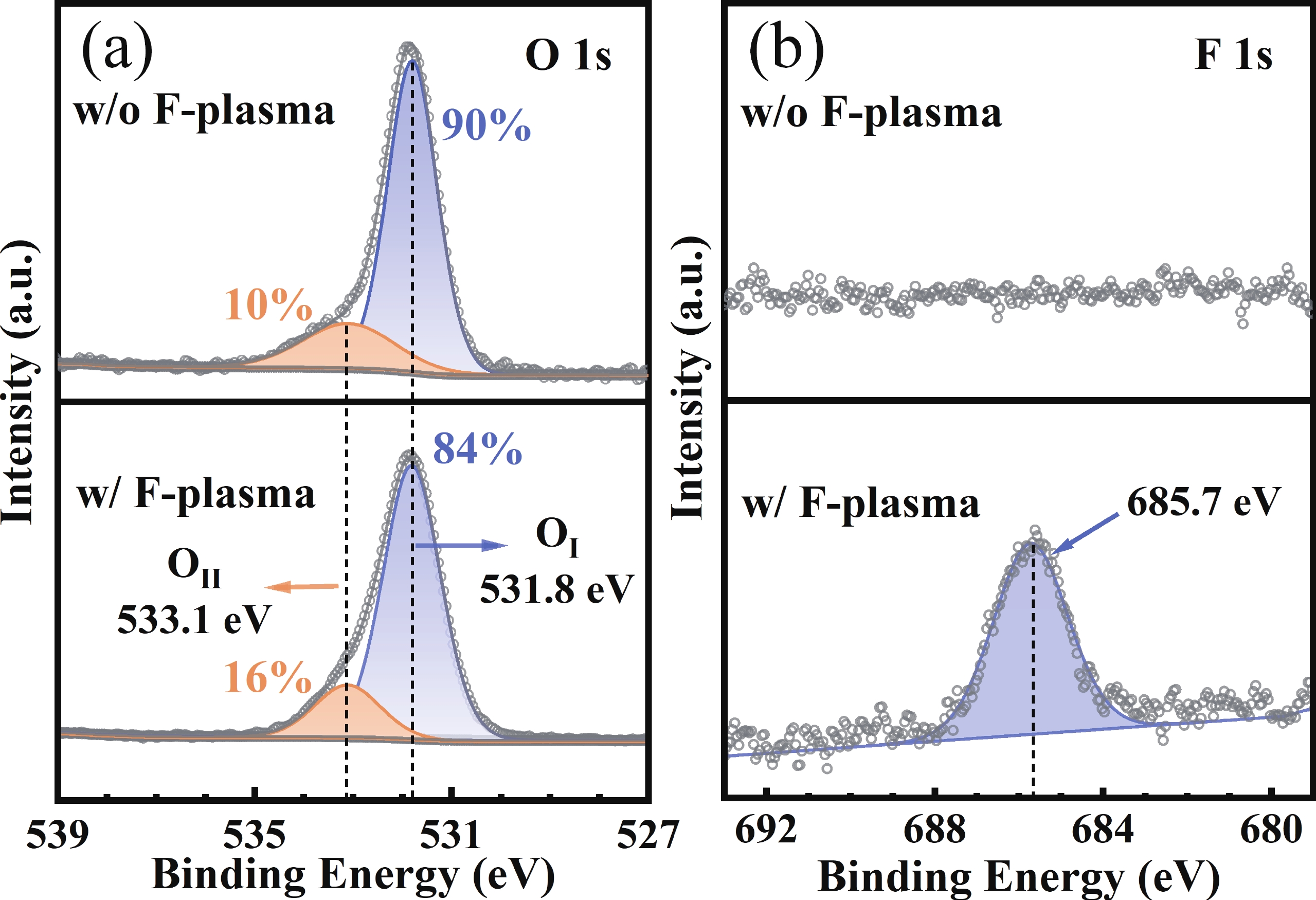
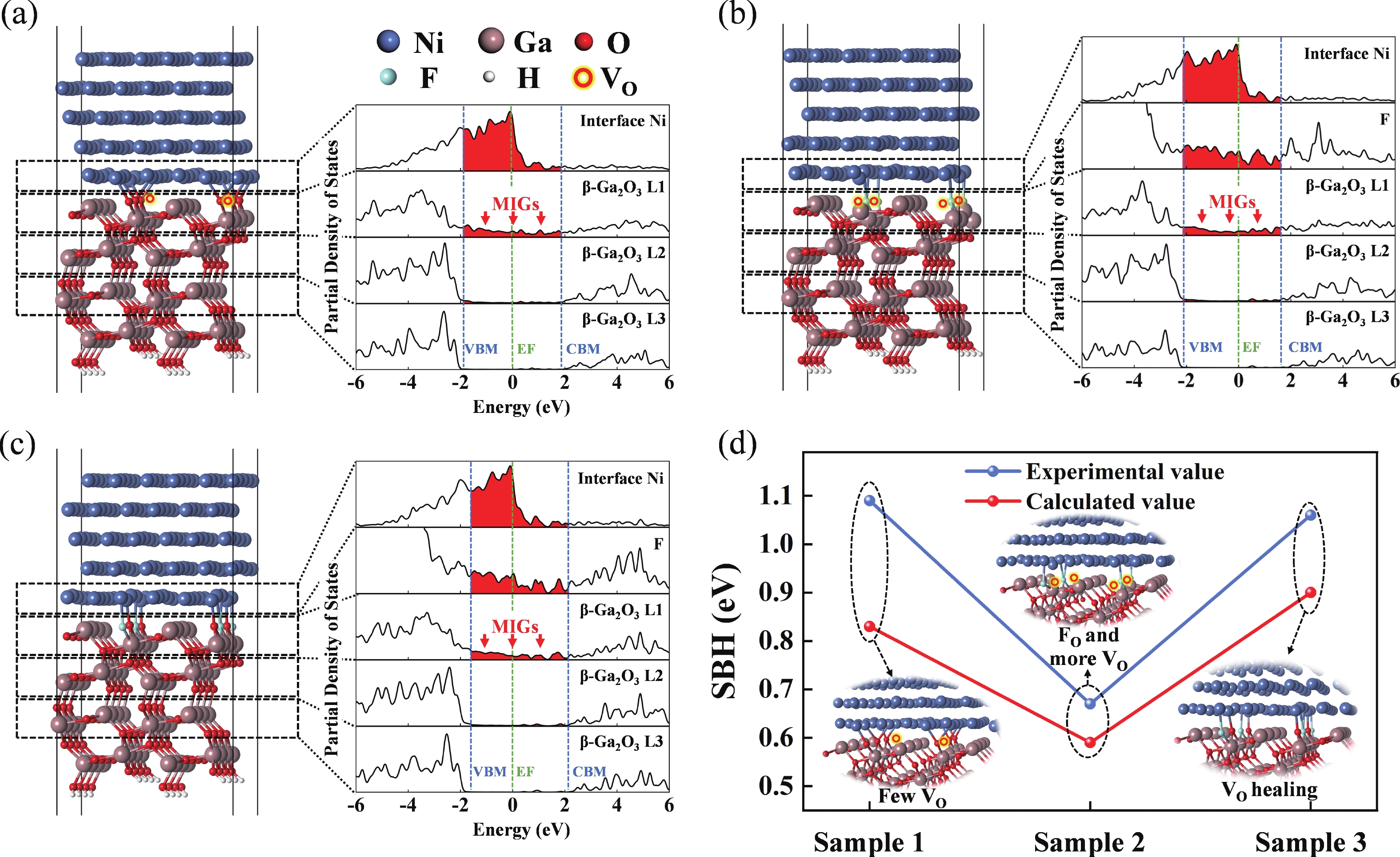
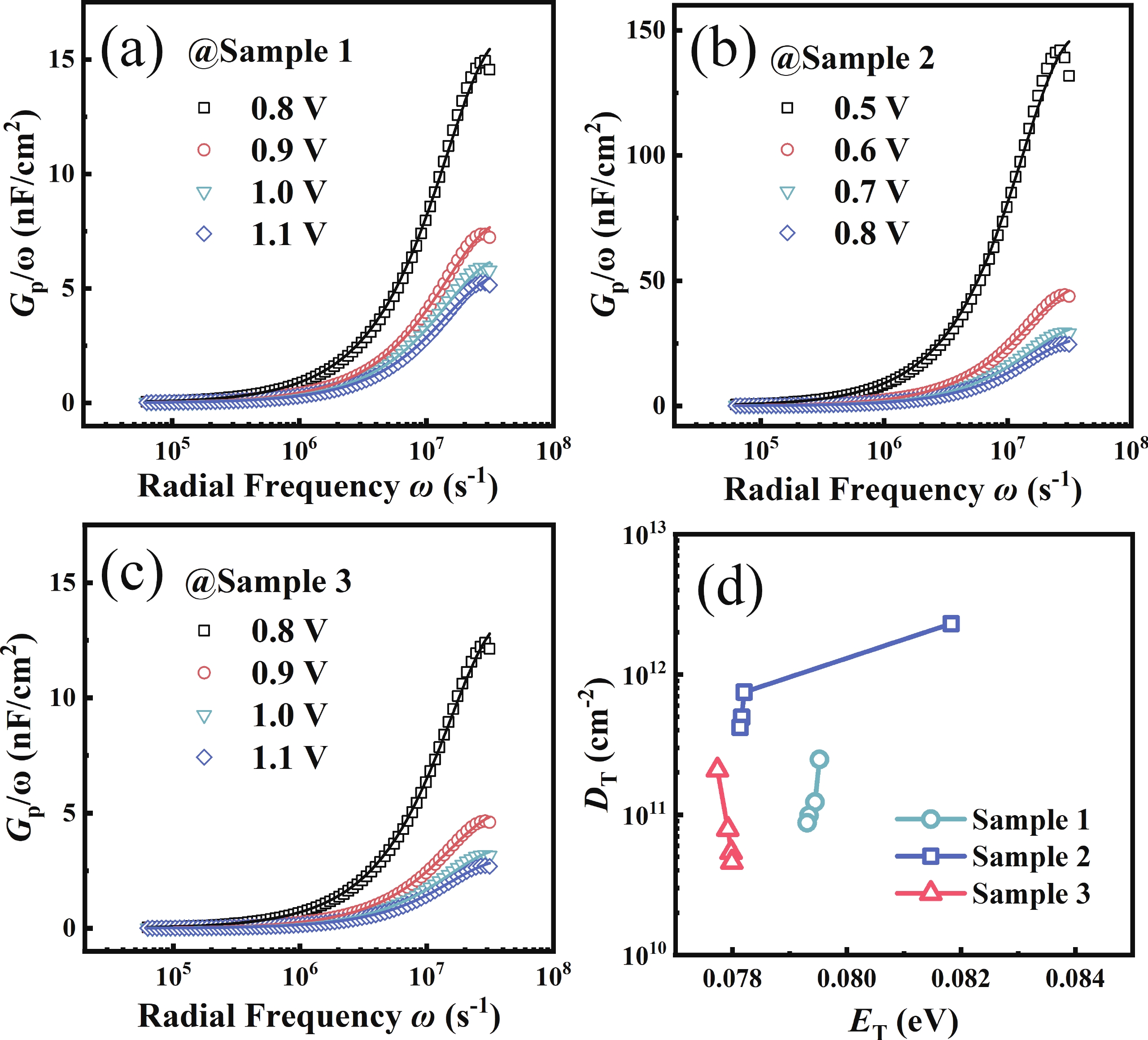
The interfacial properties of Schottky contacts crucially affect the performance of power devices. While a few studies have explored the impact of fluorine on Schottky contacts, a comprehensive theoretical explanation supported by experimental evidence remains lacking. This work investigates the effects of fluorine incorporation and electrothermal annealing (ETA) on the current transport process at Ni/β-Ga2O3 Schottky contacts. X-ray photoelectron spectroscopy and first-principles calculations confirm the presence of fluorine substitutions for oxygen and oxygen vacancies and their lowering effect on the Schottky barrier heights. Additionally, accurate electrothermal hybrid TCAD simulations validates the extremely short-duration high temperatures (683 K) induced by ETA, which facilitates lattice rearrangement and reduces interface trap states. The interface trap states are quantitatively resolved through frequency-dependent conductance technique, showing the trap density (DT) reduction from (0.88−2.48) × 1011 cm−2·eV−1 to (0.46−2.09) × 1011 cm−2·eV−1. This investigation offers critical insights into the β-Ga2O3 contacts with the collaborative treatment and solids the promotion of high-performance β-Ga2O3 power devices.
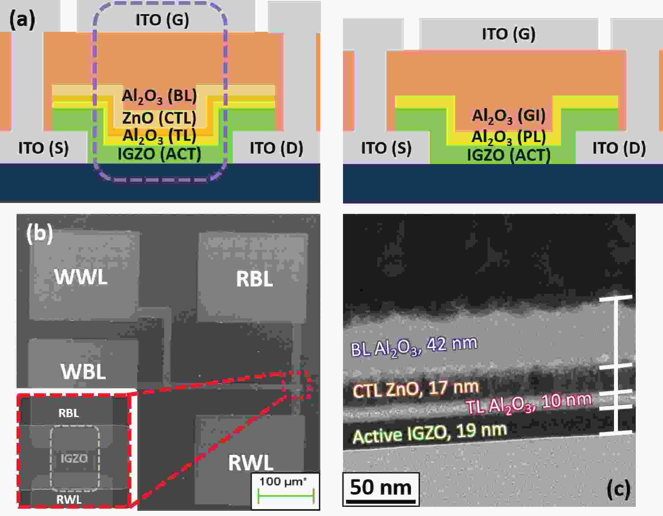
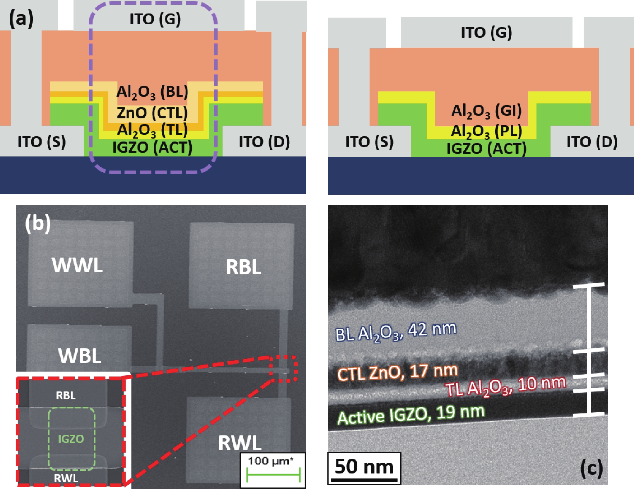
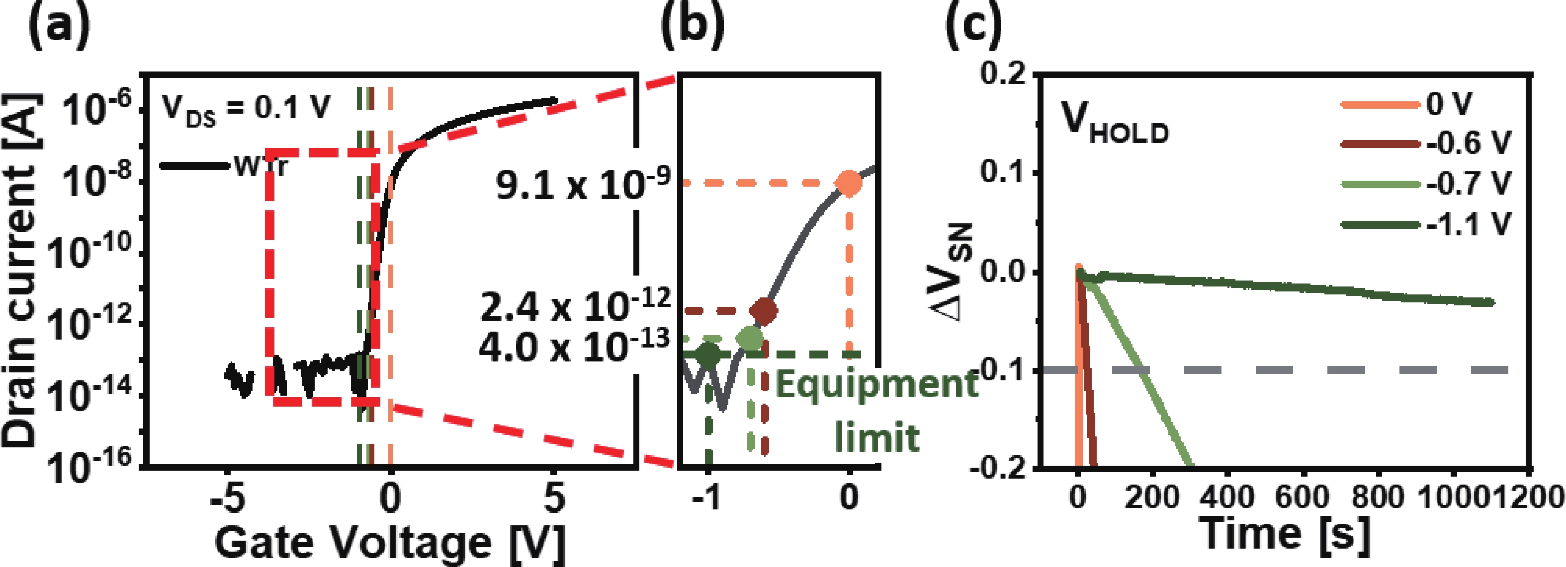
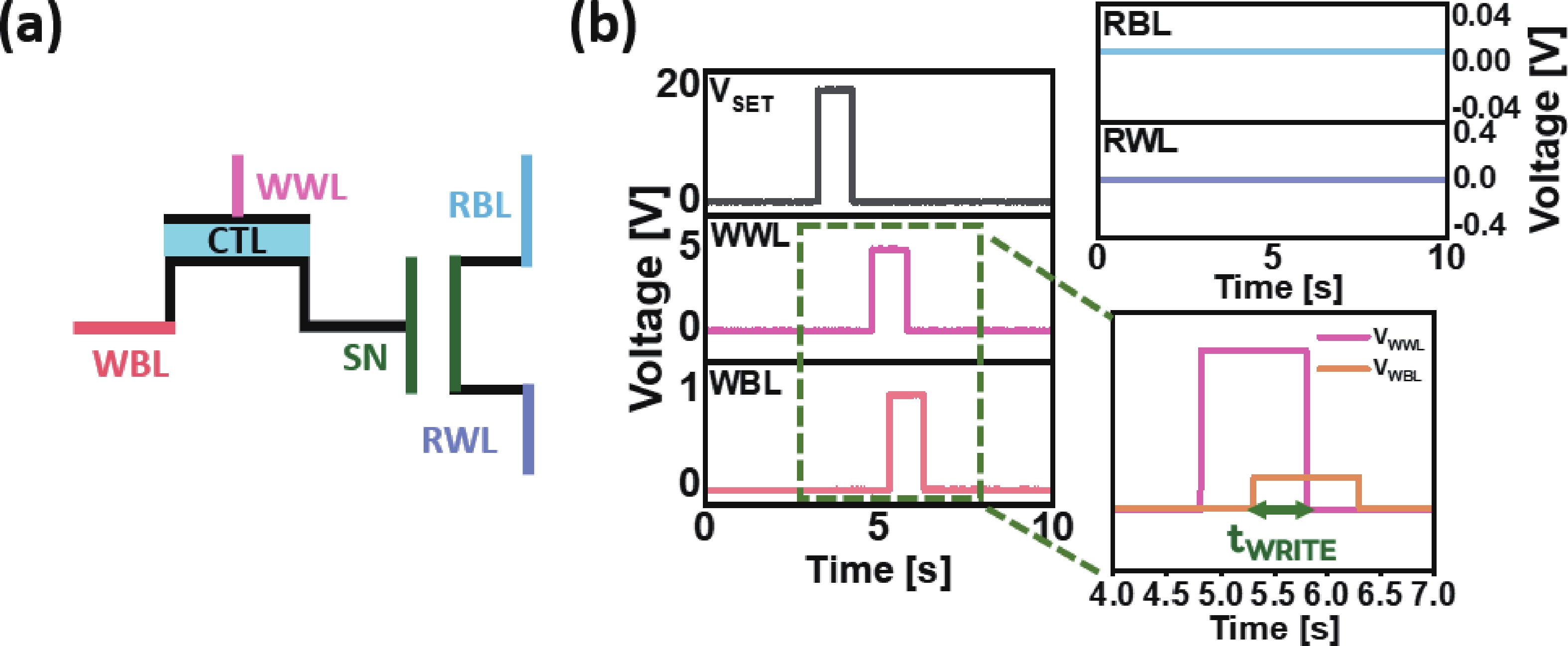
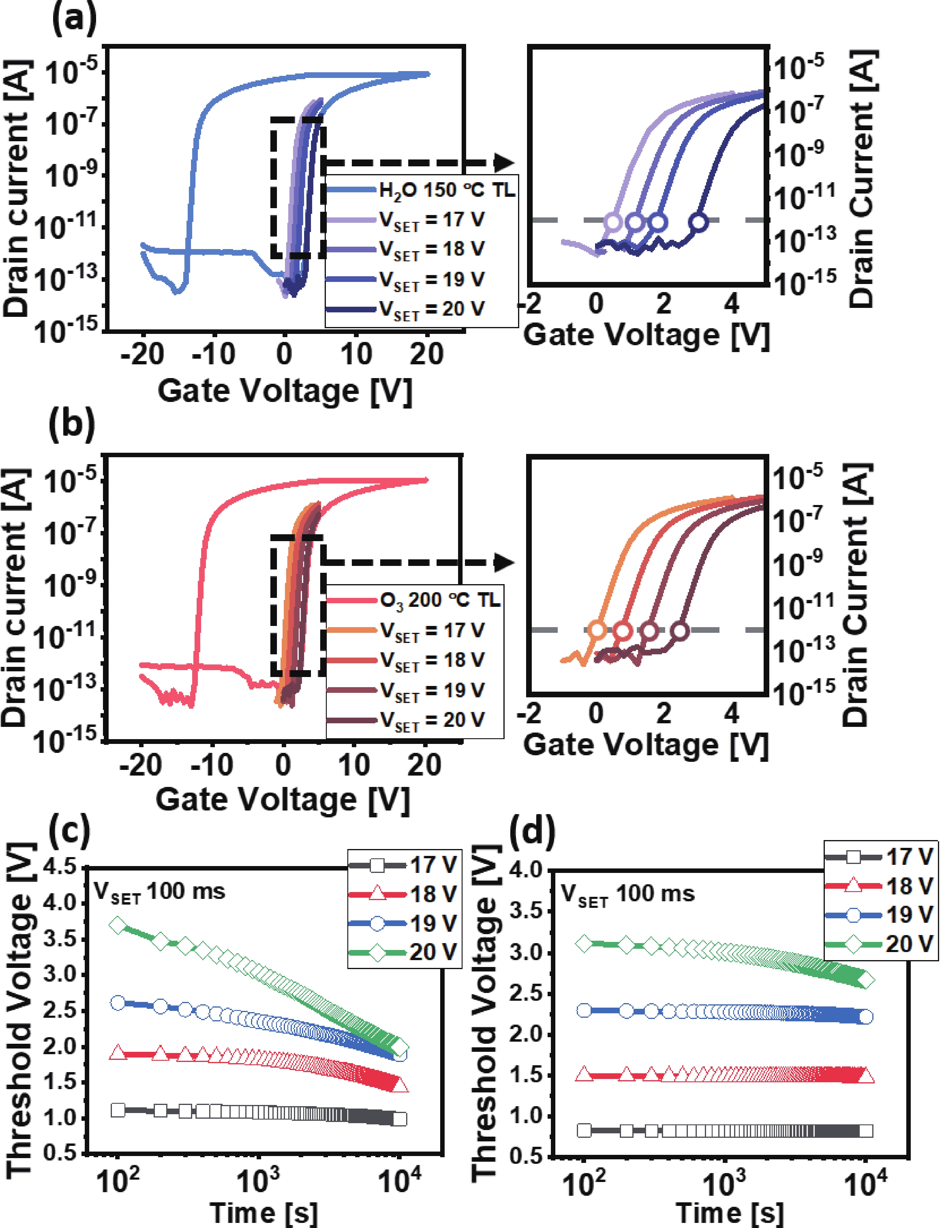
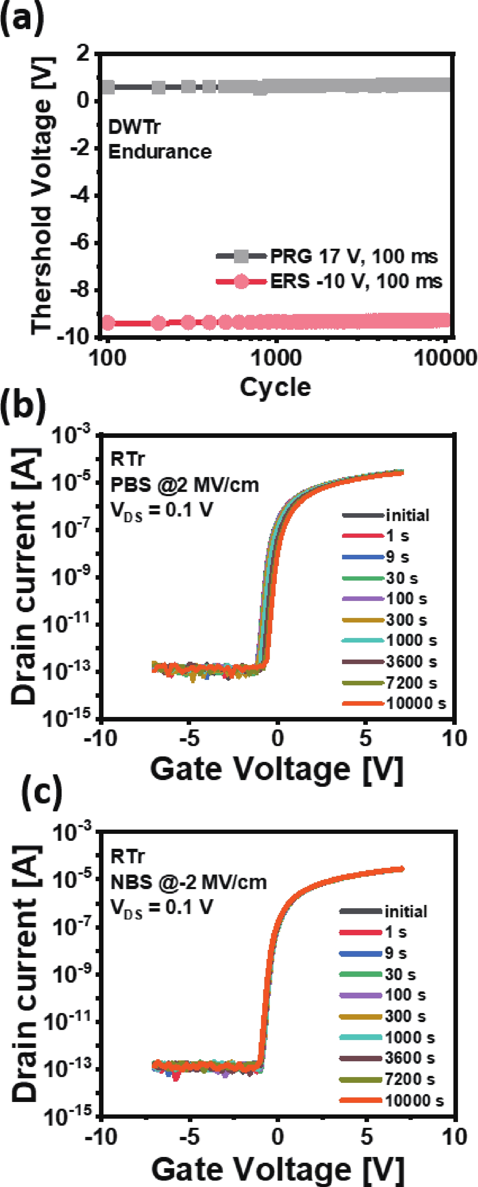
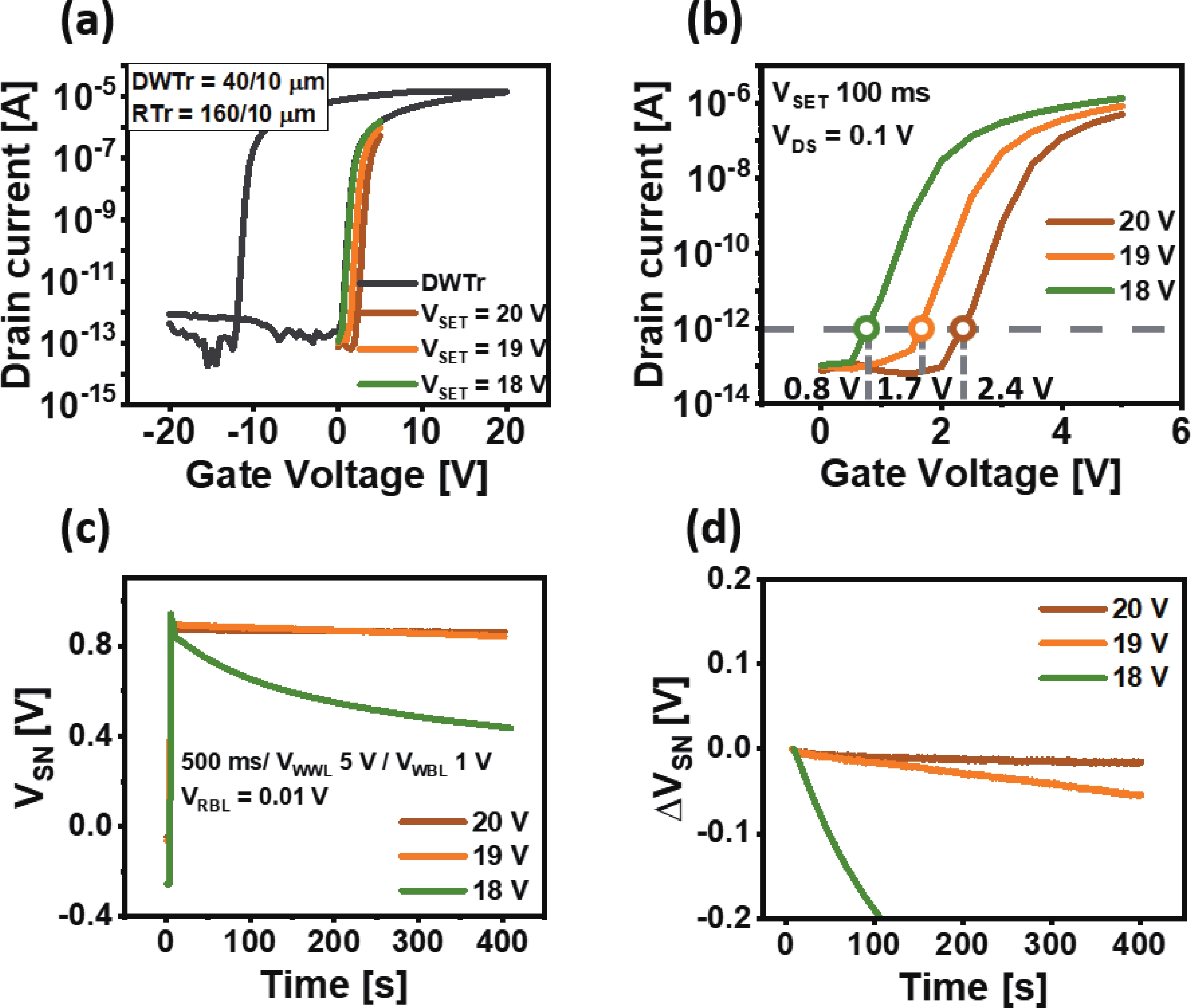
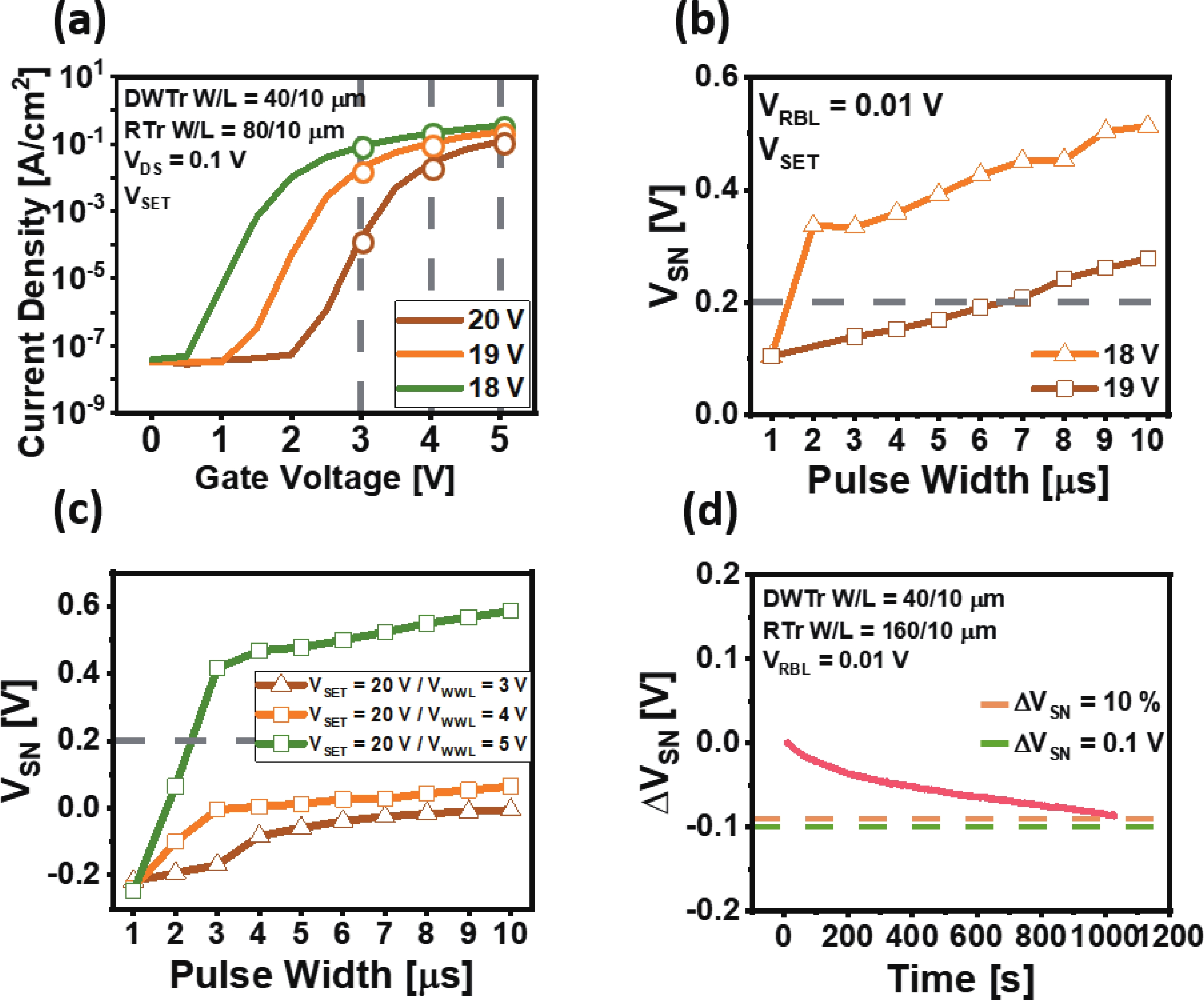
The fabrication of a dynamic threshold-2T0C (DT-2T0C) DRAM cell incorporating a ZnO charge-trap layer in the write transistor has been successfully achieved, addressing the negative hold voltage (VHOLD) issue of conventional 2T0C DRAM cells using oxide channel layers. The proposed device facilitates dynamic modulation of turn-on voltage (VON) through an additional SET operation, allowing VON to shift above 0 V. The retention time in SET operation was extended to 104 s by optimizing the tunneling layer deposition conditions. The device characterization revealed a significant correlation between VON and both the WRITE speed and the retention properties of the DT-2T0C, verifying the trade-off between WRITE time and retention time. A long retention time over 1000 s was achieved, even under VHOLD of 0 V.

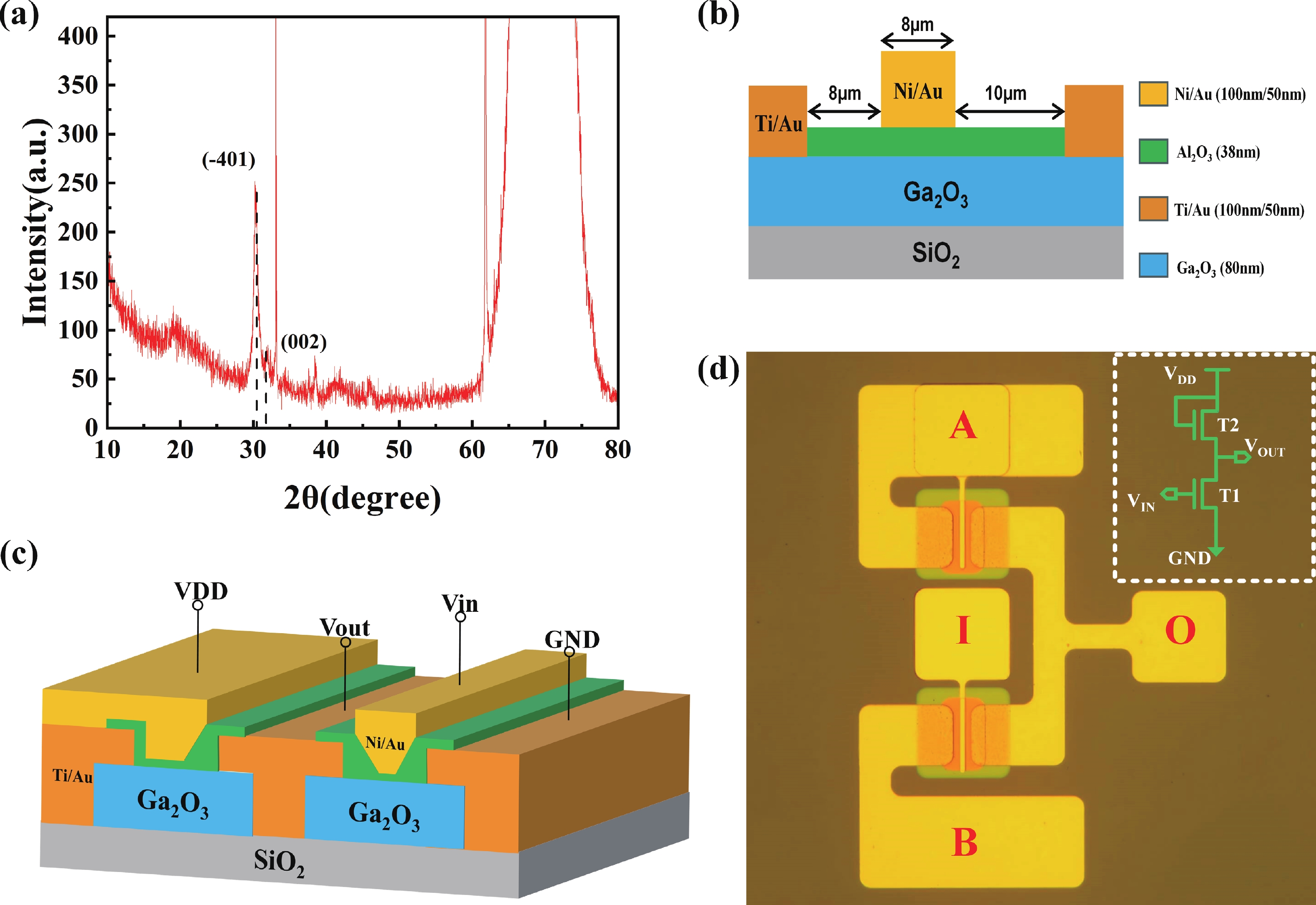
β-Ga2O3 MOS inverter should play a crucial role in β-Ga2O3 electronic circuits. Enhancement-mode (E-mode) MOSFET was fabricated based on β-Ga2O3 film grown by atomic layer deposition technology, and the β-Ga2O3 inverter was further monolithically integrated on this basis. The β-Ga2O3 nMOSFET exhibits excellent electrical characteristics with an on/off current ratio reaching 105. The logic inverter shows outstanding voltage inversion characteristics under low-frequency from 1 to 400 Hz operation. As the frequency continues to increase to 10 K, the reverse characteristic becomes worse due to parasitic capacitance induced by processes, and the difference between the highest and lowest values of VOUT has an exponential decay relationship with the frequency. This paper provides the practice for the development of β-Ga2O3-based circuits.


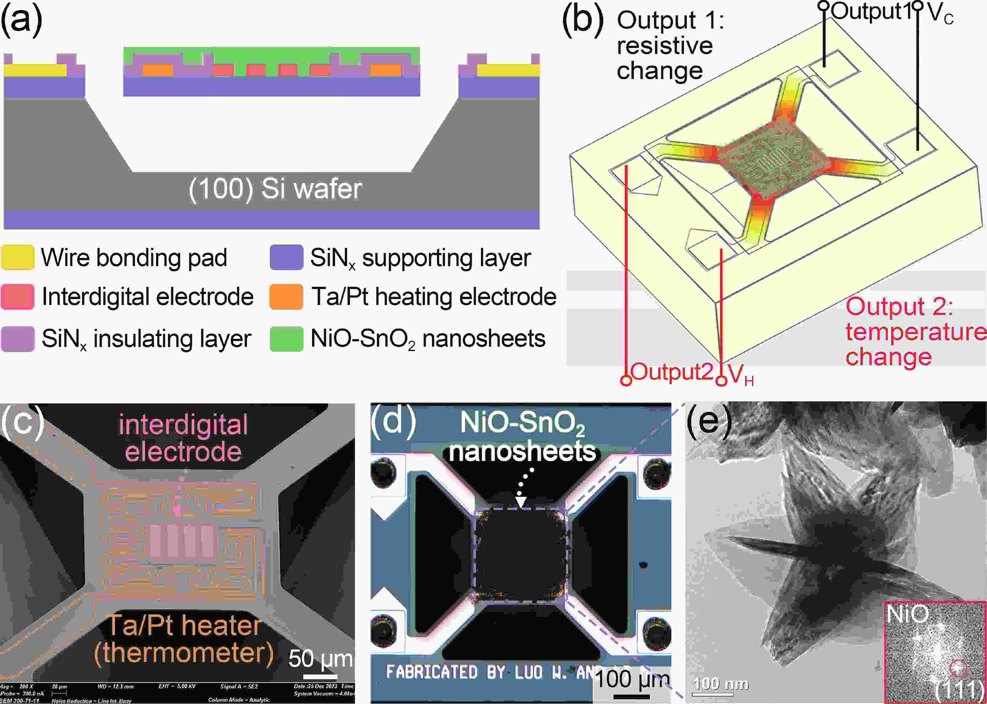
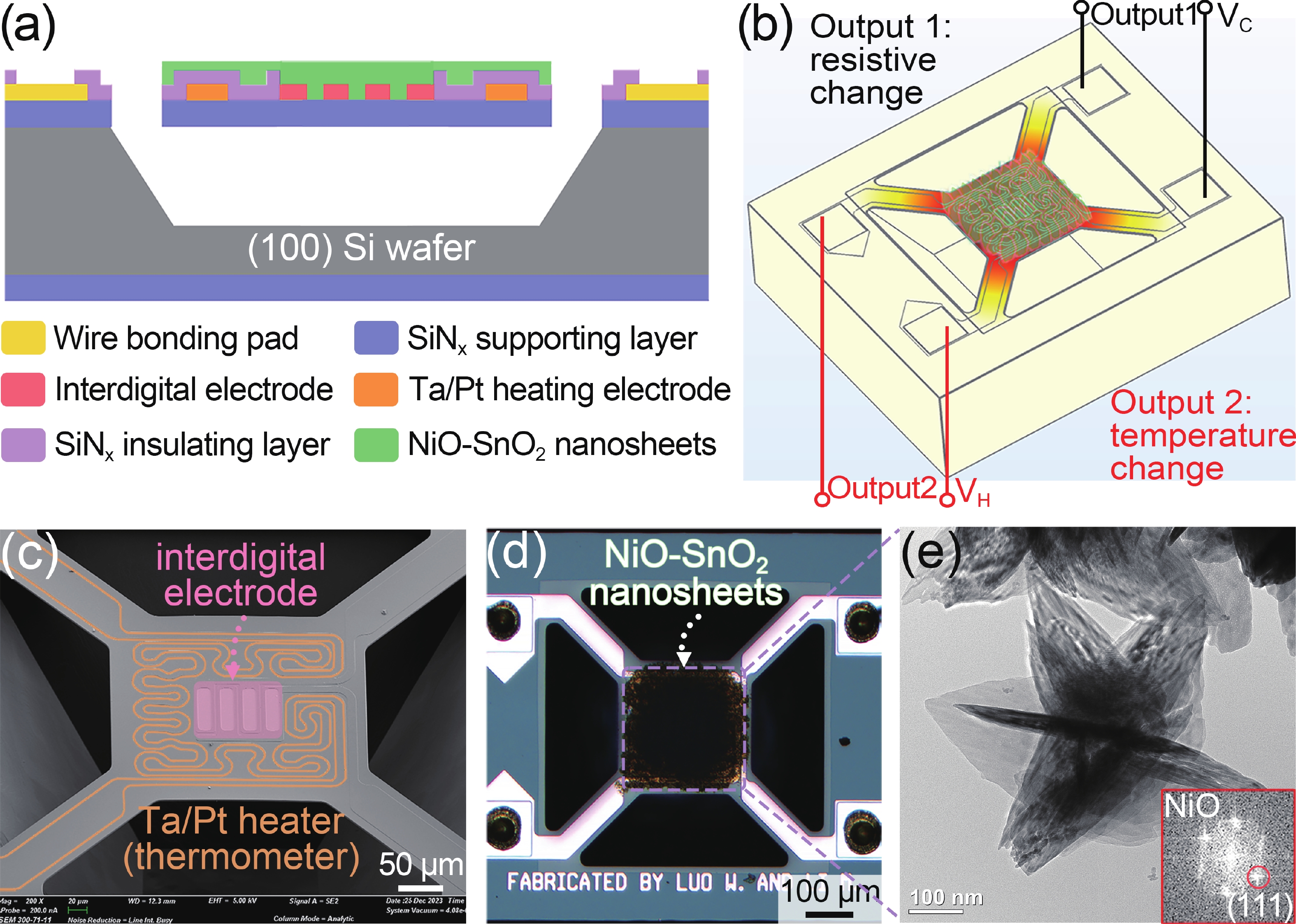
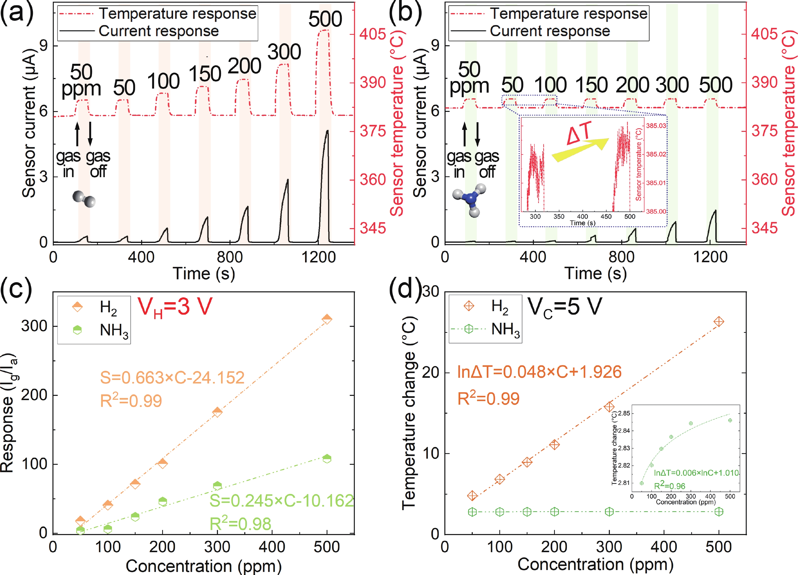
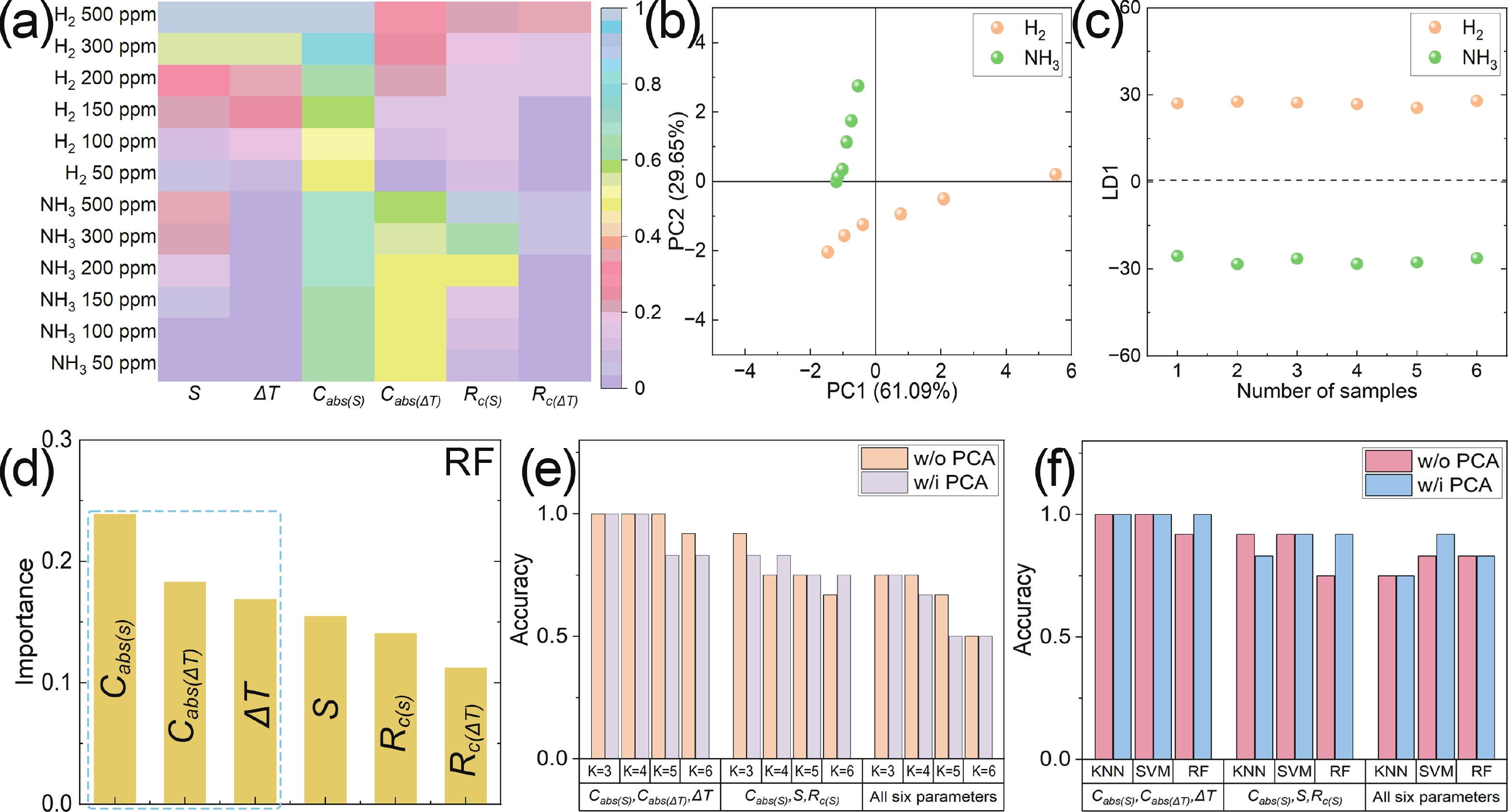
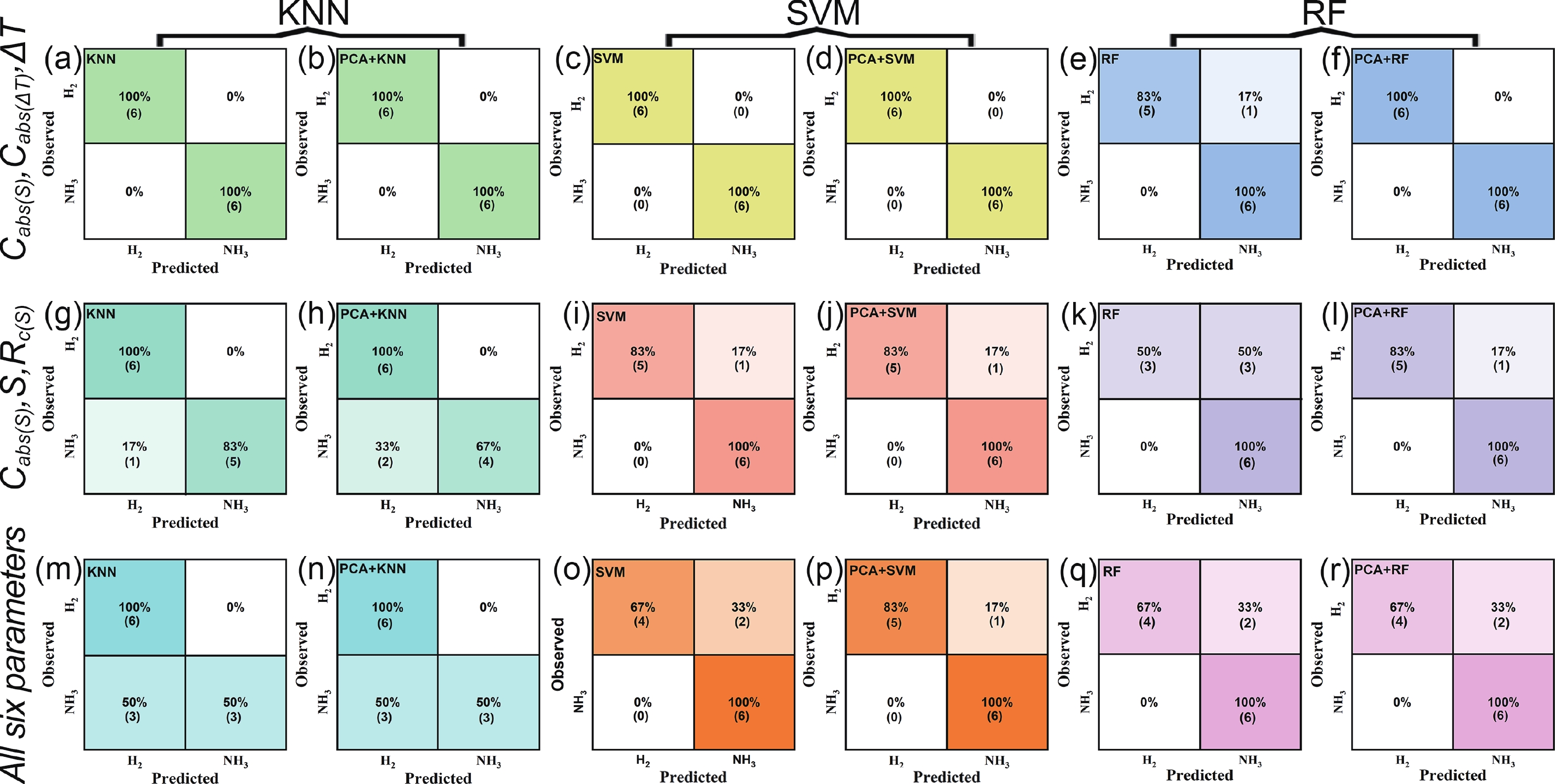
Selectivity remains a significant challenge for gas sensors. In contrast to conventional gas sensors that depend solely on conductivity to detect gases, we exploited a single NiO-doped SnO2 sensor to simultaneously monitor transient changes in both sensor conductivity and temperature. The distinct response profiles of H2 and NH3 gases were attributed to differences in their redox rates and enthalpy changes during chemical reactions, which provided an opportunity for gas identification using machine learning (ML) algorithms. The test results indicate that preprocessing the extracted calorimetric and chemi-resistive parameters using the principal component analysis (PCA), followed by the application of ML classifiers for identification, enables a 100% accuracy for both target analytes. This work presents a facile gas identification method that enhances chip-level sensor applications while minimizing the need for complex sensor arrays.
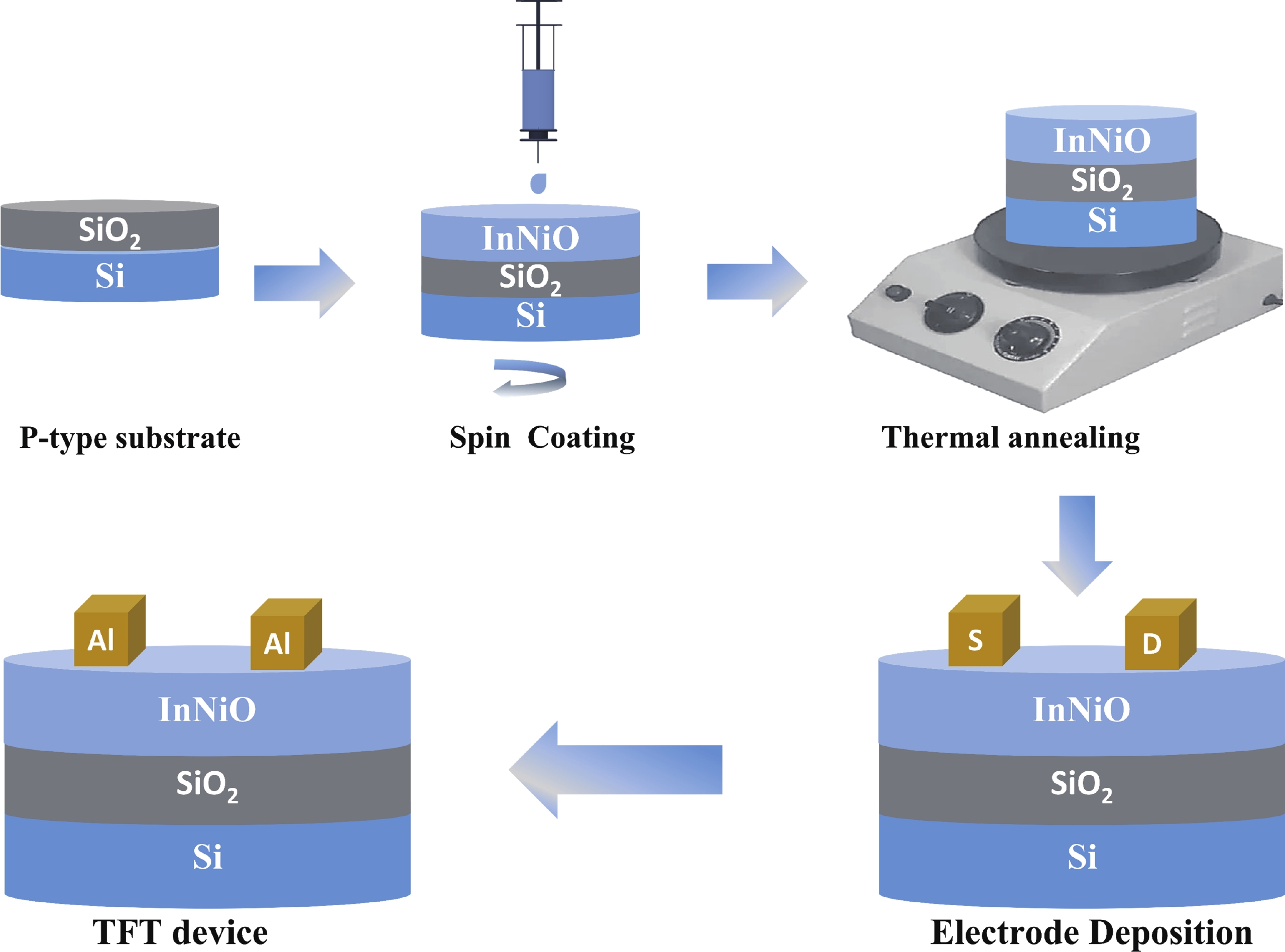
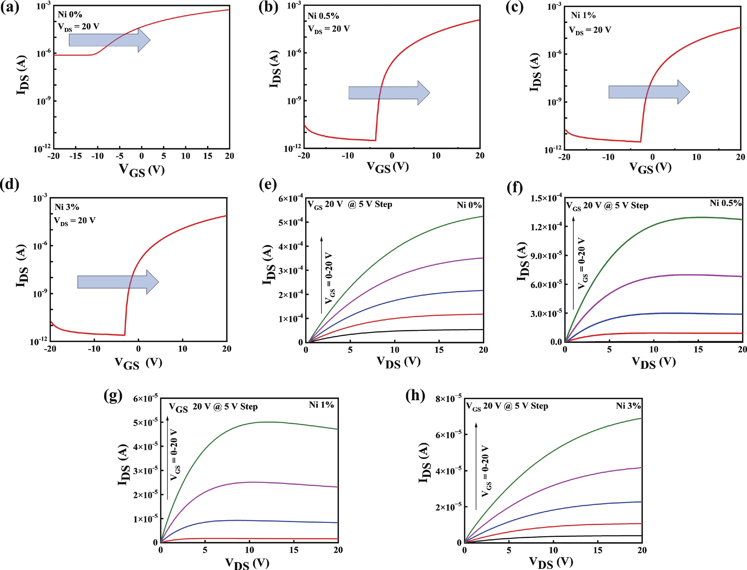
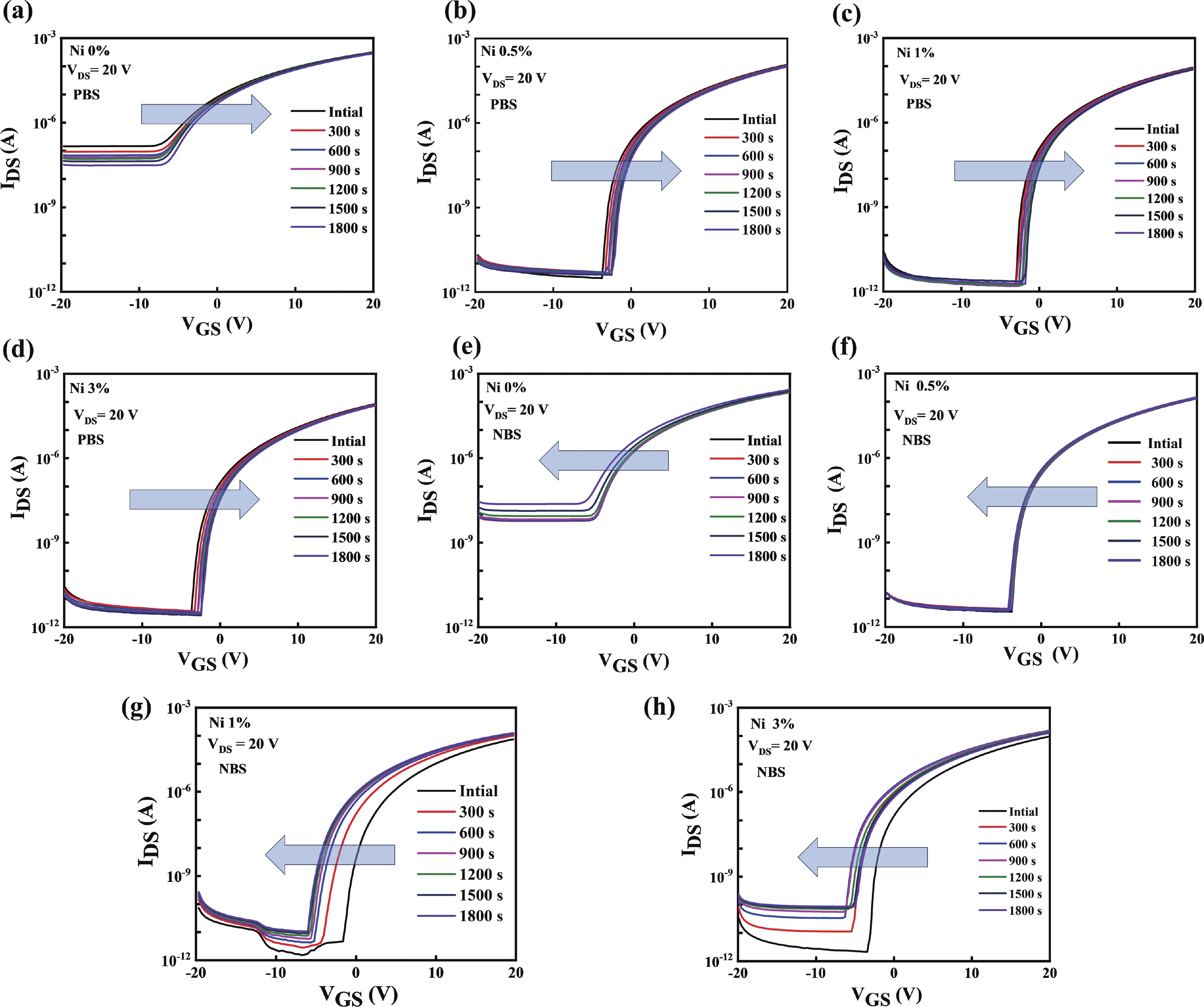
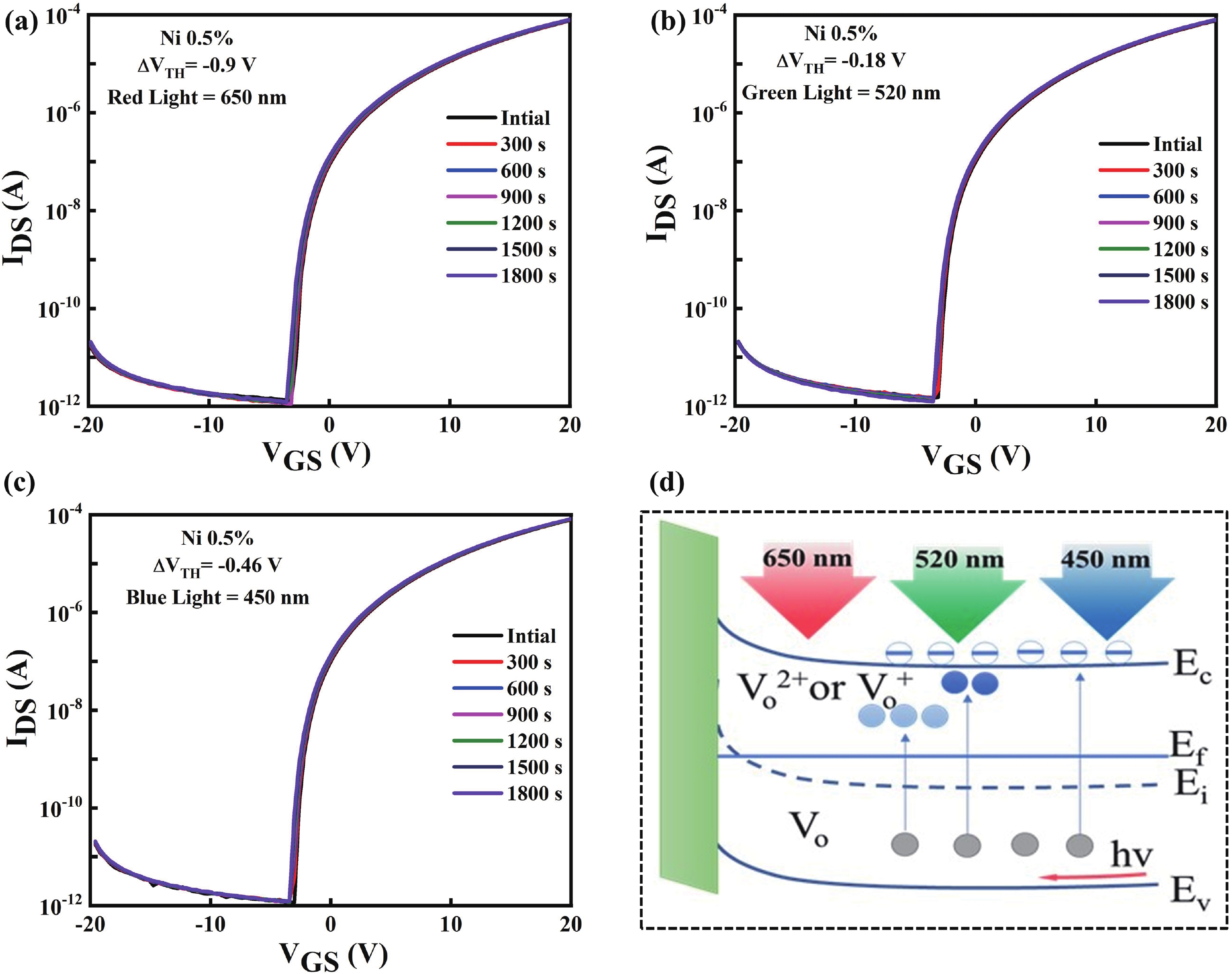
Doping in thin-film transistors (TFTs) plays a crucial role in tailoring material properties to enhance device performance, making them essential for advanced electronic applications. This study explores the synthesis and characterization of TFTs fabricated using nickel (Ni)-doped indium oxide (In2O3) via a wet-chemical approach. The presented work investigates the effect of "Ni" incorporation in In2O3 on the structural and electrical transport properties of In2O3, revealing that higher "Ni" content decreases the oxygen vacancies, leading to a reduction in leakage current and a forward shift in threshold potential (Vth). Experimental findings reveal that NiInO-based TFTs (with Ni = 0.5%) showcase enhanced electrical performance, achieving mobility of 7.54 cm2/(V∙s), an impressive ON/OFF current ratio of ~107, a Vth of 6.26 V, reduced interfacial trap states (Dit) of 8.23 × 1012 cm−2 and enhanced biased stress stability. The efficacy of "Ni" incorporation is attributed to the upgraded Lewis acidity, stable Ni−O bond strength, and small ionic radius of Ni. Negative bias illumination stability (NBIS) measurements further indicate that device stability diminishes with shorter light wavelengths, likely due to the activation of oxygen vacancies. These findings validate the solution-processed techniques' potential for future large-scale, low-cost, energy-efficient, and high-performance electronics.


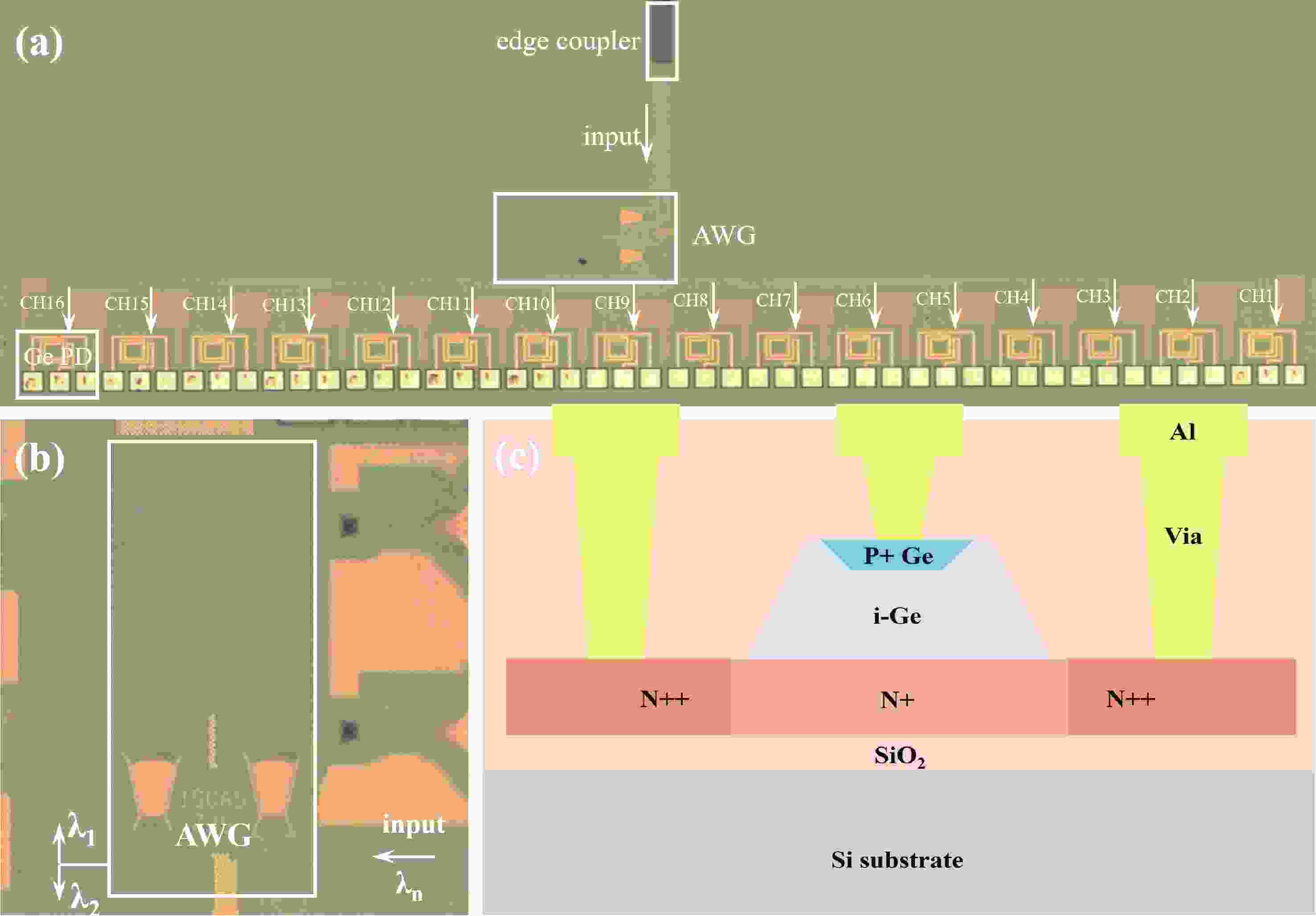
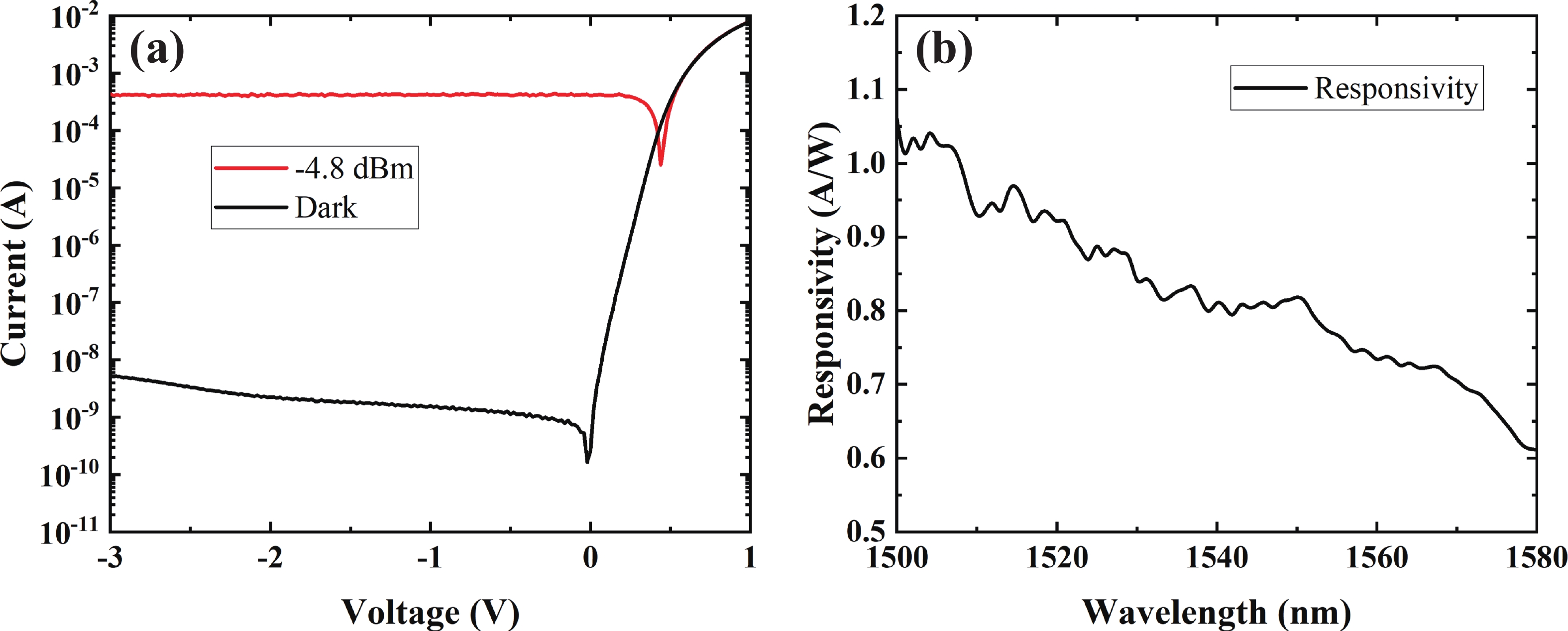
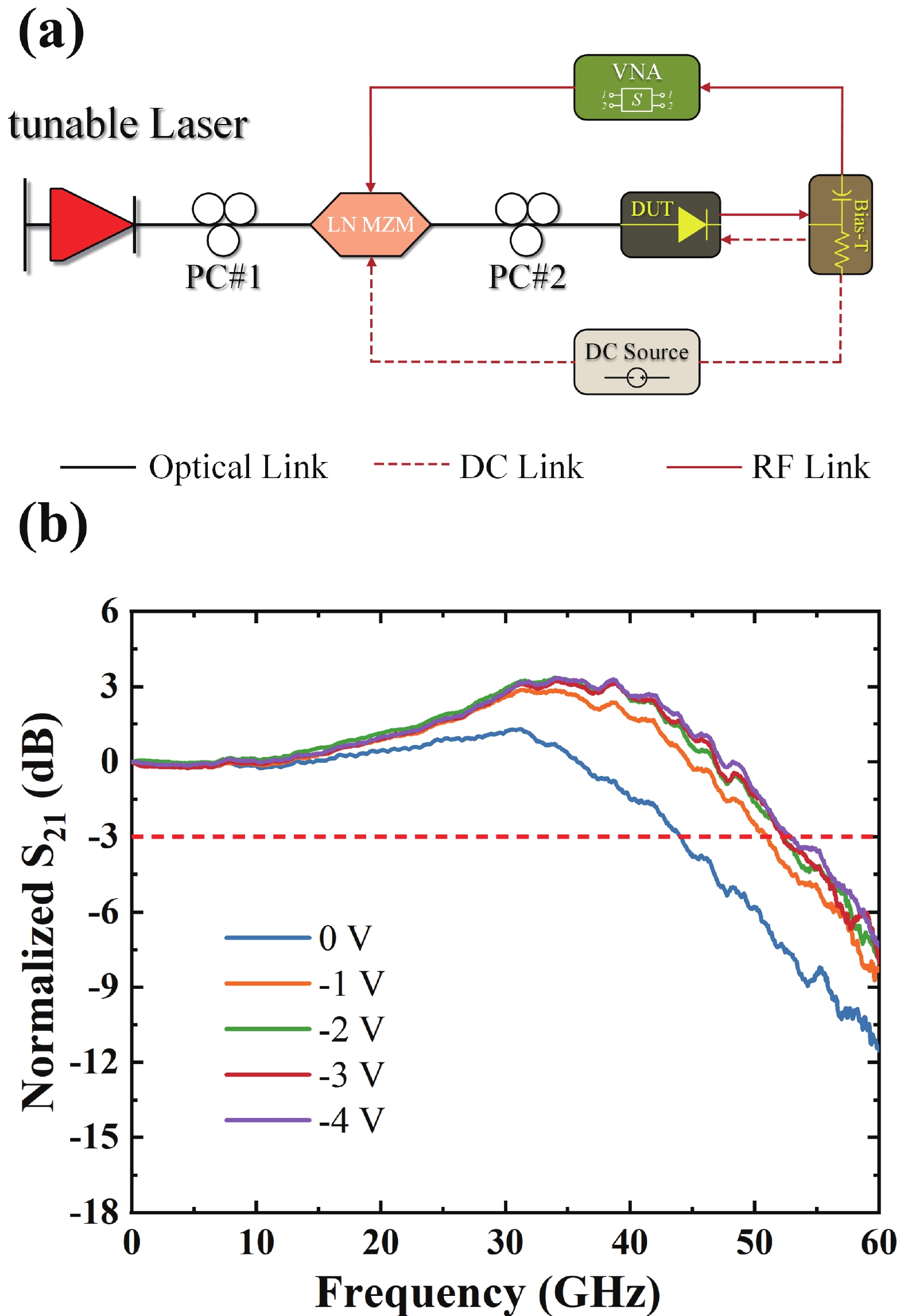
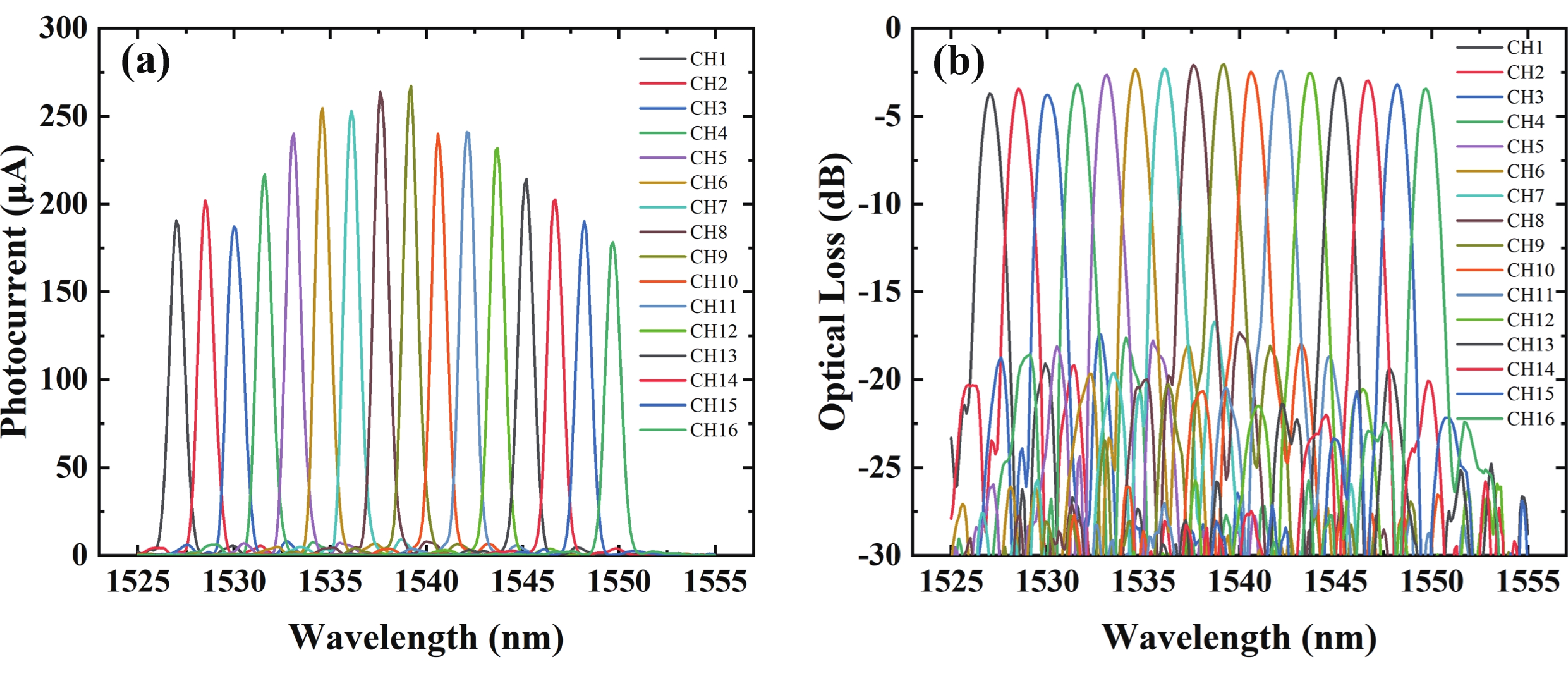
Wavelength division multiplexing technology has been pivotal in addressing the demand for high-capacity optical communication with silicon photonics providing a promising platform. This work presents a 16-channel wavelength division multiplexing silicon photonics receiver chip composed of an arrayed waveguide grating and Ge-on-Si photodetectors. Integrated inductors are introduced to enhance the high-speed performance of photodetectors, enabling data rates up to 112 Gbps with high responsivity and low dark current. The operating wavelength range of the arrayed wavelength grating is adjusted according to the response of the Ge-on-Si photodetector. The optical insertion loss, cross talk and central wavelength of the array waveguide grating are 2.1 to 3.7 dB, −12 to −15 dB, and 1538 nm, respectively. The proposed receiver chip offers a solution to meet the challenges of modern data transmission requirements.


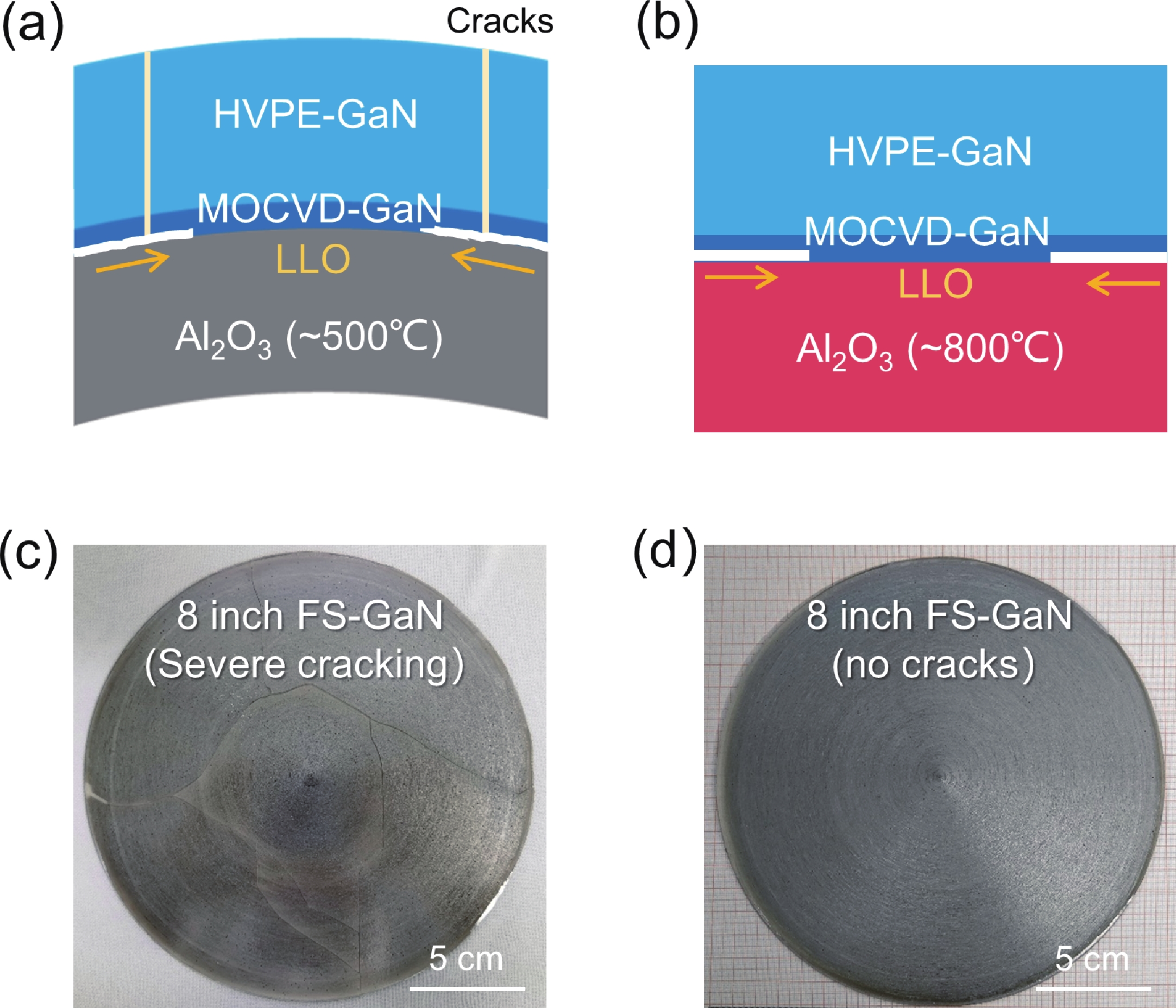
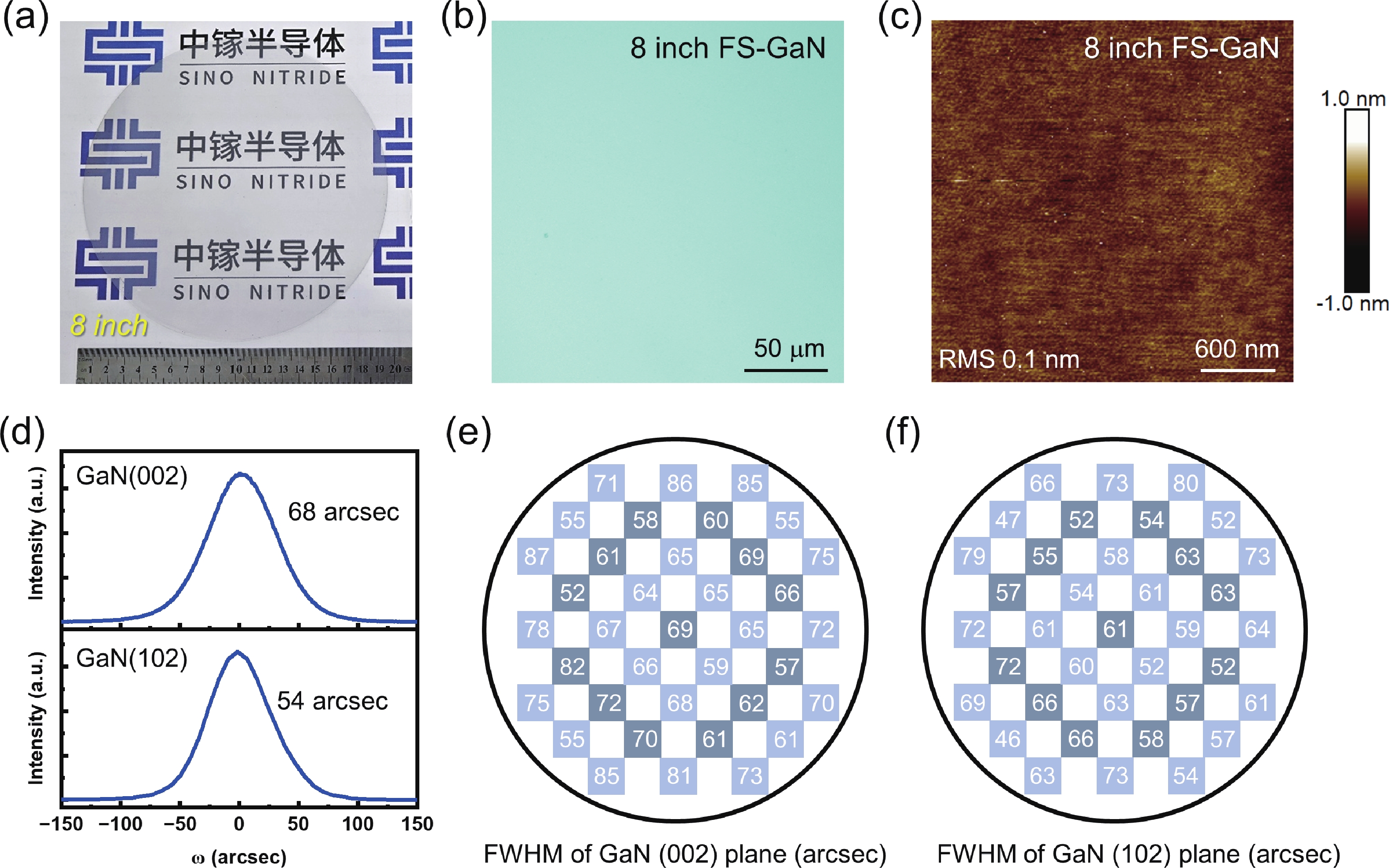
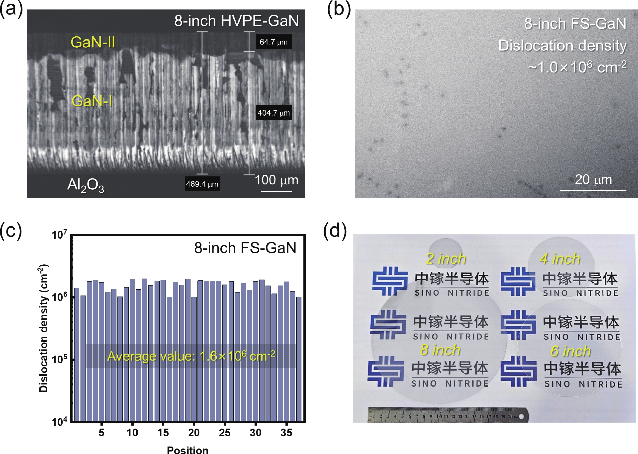
The absence of large-size gallium nitride (GaN) substrates with low dislocation density remains a primary bottleneck for advancing GaN-based devices. Here, we demonstrate the achievement of 8-inch freestanding GaN substrates grown by hydride vapor phase epitaxy. Critical to this achievement is the improvement in gas-flow uniformity, which ensures exceptional thickness homogeneity and enables the crack-free growth of GaN. After laser lift-off (LLO) separation, the freestanding GaN substrate exhibits superior crystal quality, evidenced by full width at half maximum values of 68 and 54 arcsec for X-ray diffraction rocking curves of (002) and (102) planes, alongside a low dislocation density of 1.6 × 106 cm−2. This approach establishes a robust pathway for the production of large-size GaN substrates, which are essential for advancing next-generation power electronics and high-efficiency photonics.

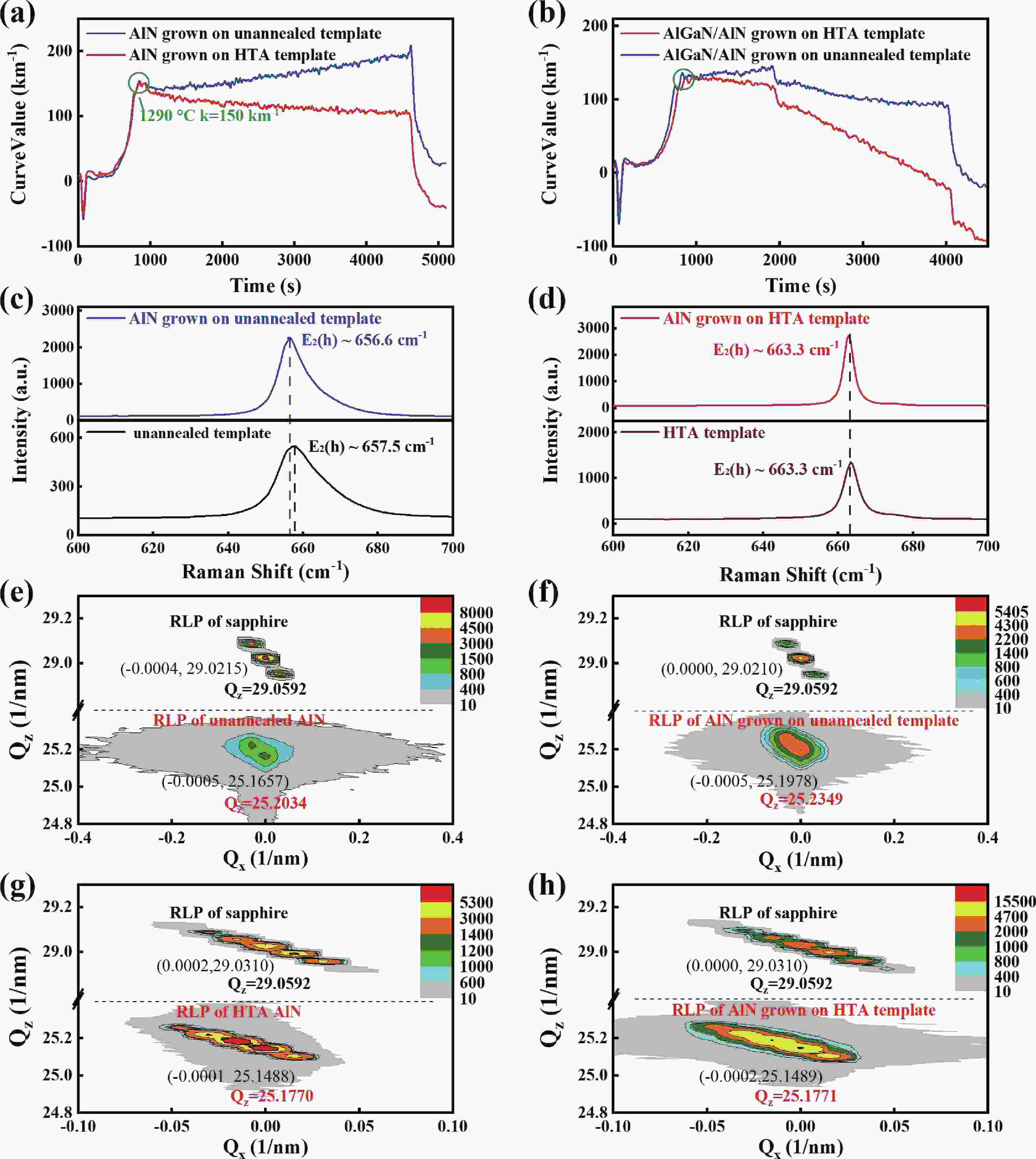
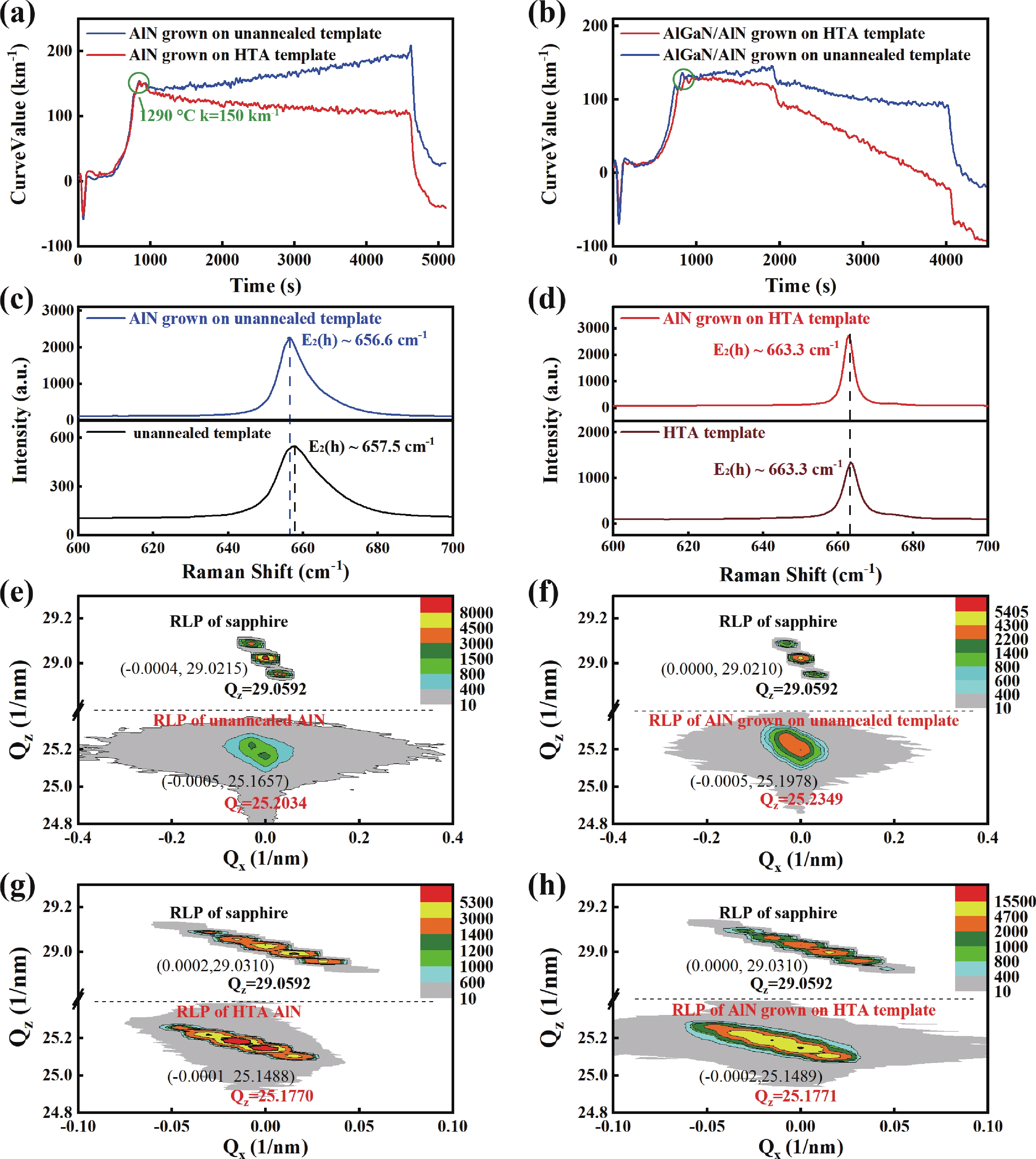
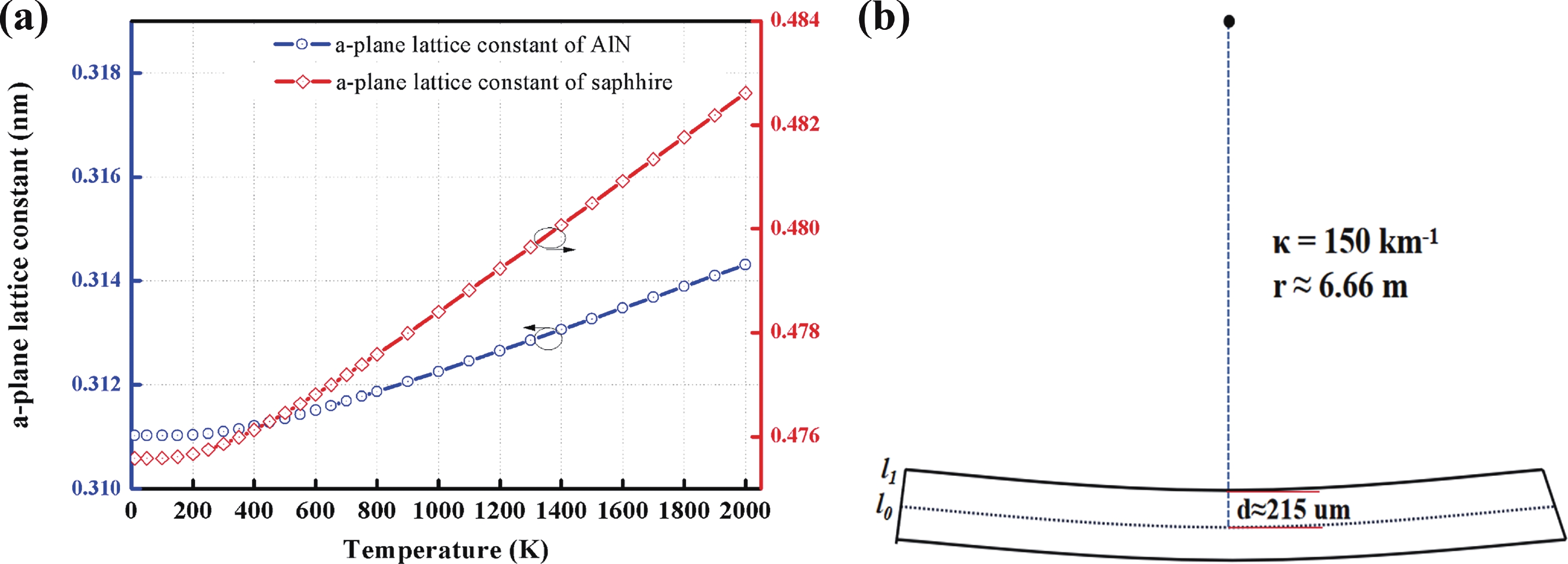
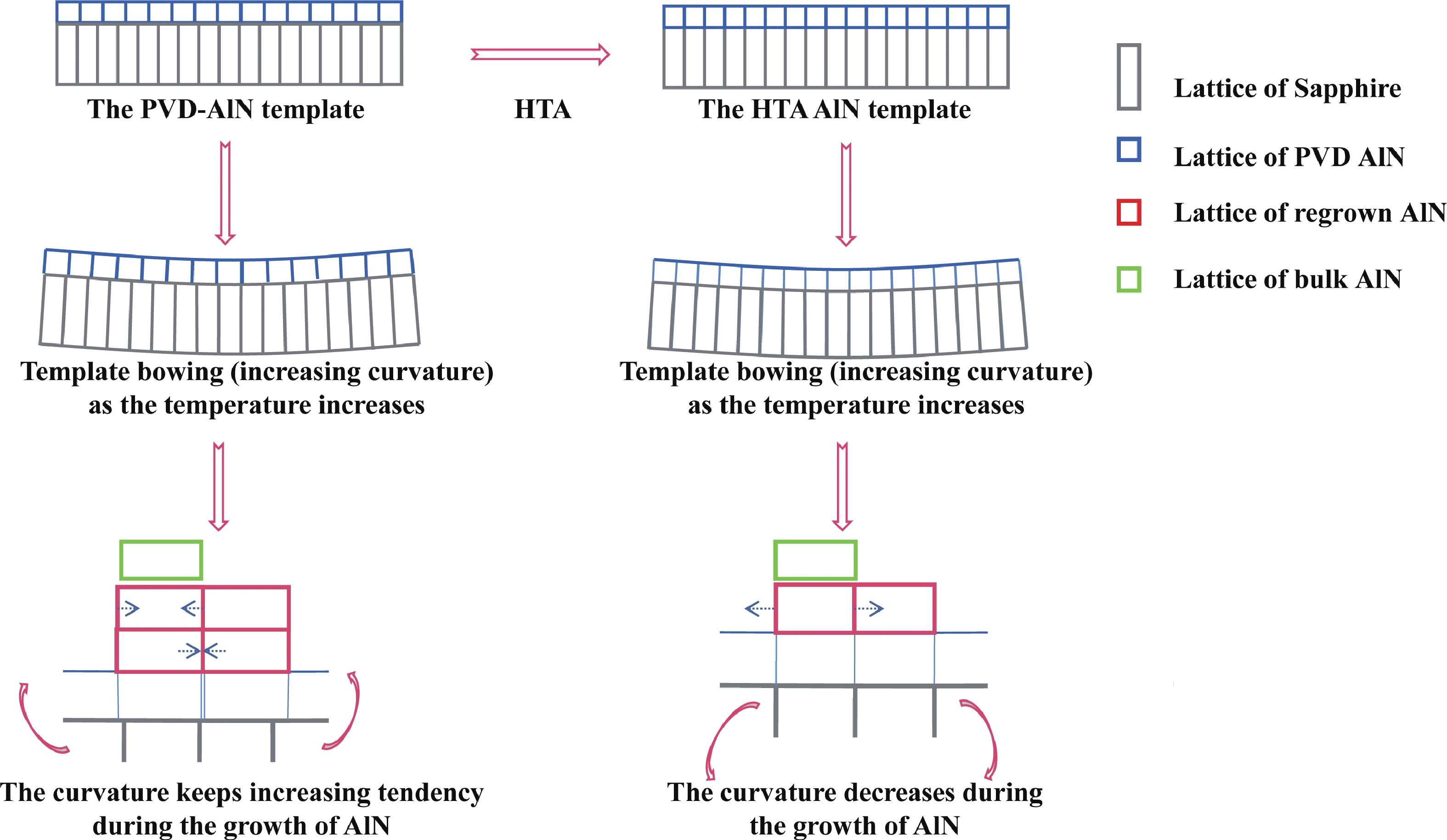
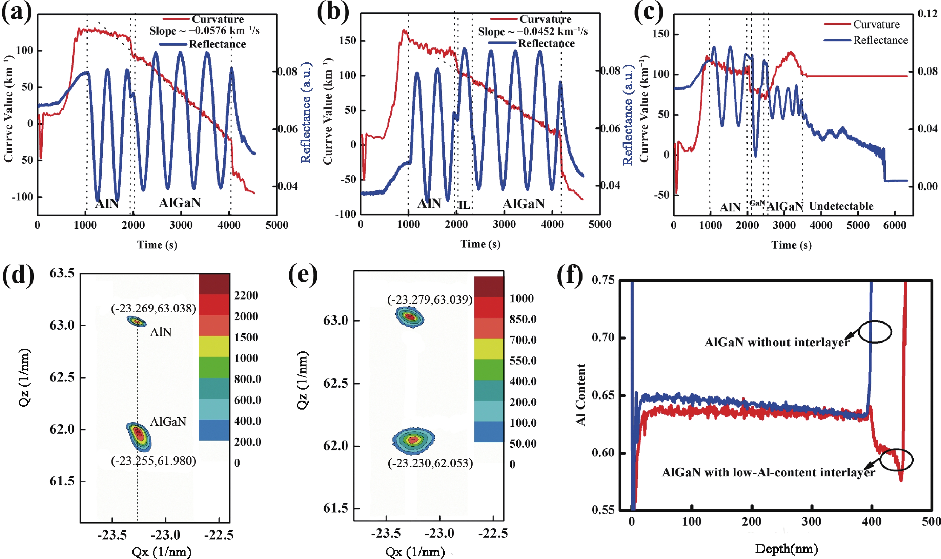
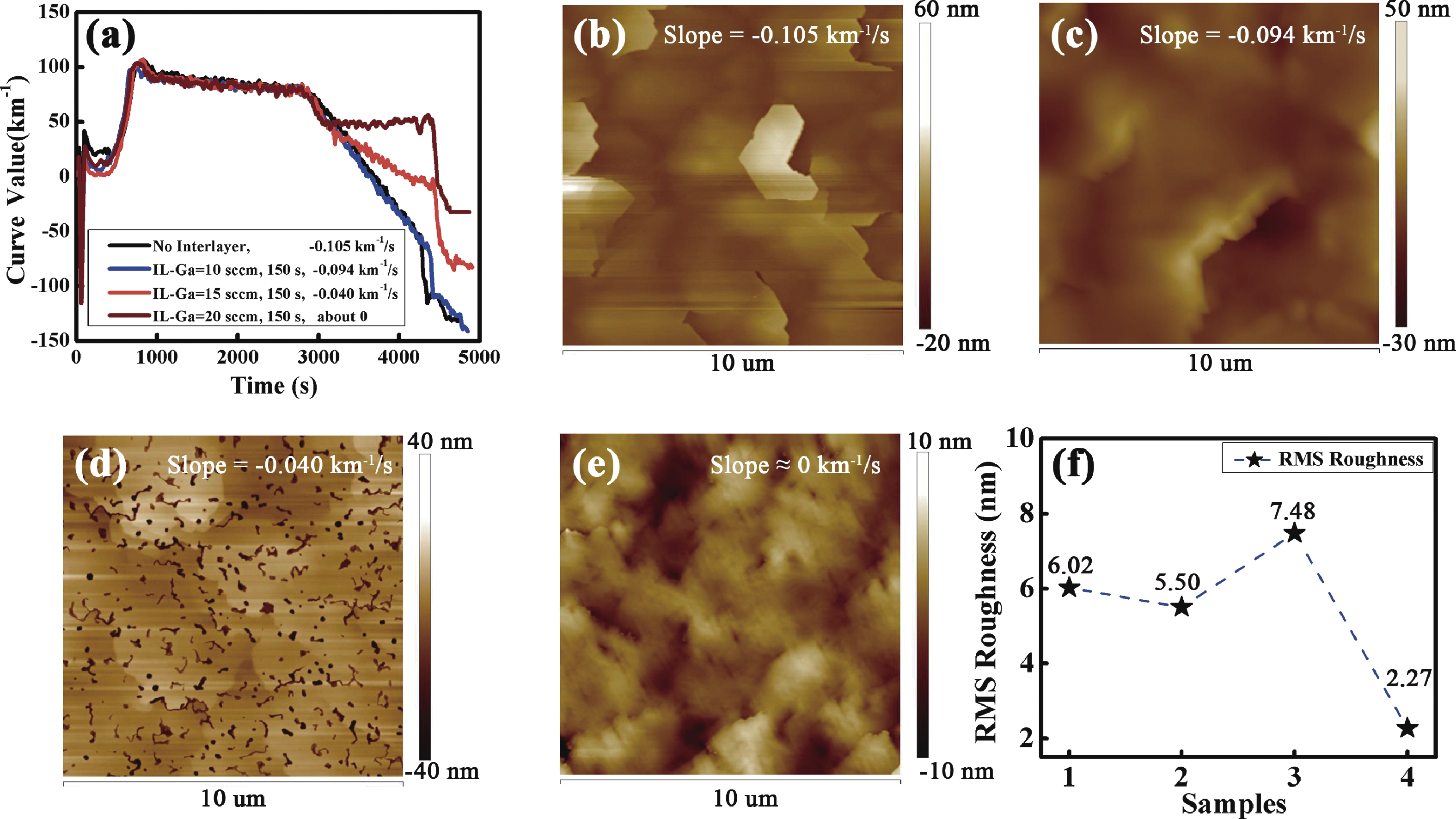
High-temperature-annealed AlN (HTA-AlN) templates provide ideal substrates for high-quality AlGaN epitaxy. However, the significant compressive stress accumulated within the AlGaN layer makes it challenging to achieve a smooth surface free of hexagonal hillocks on these templates. To address this issue, we investigate the mechanism of compressive stress accumulation during the growth of AlGaN-based epilayers on HTA-AlN templates using in-situ curvature analysis in this study. To verify the mechanism, a low-Al-content AlGaN interlayer is introduced between the AlN epilayer and the subsequent AlGaN epilayer. The larger a-plane lattice constant of this interlayer relative to the AlGaN epilayer slows the accumulation rate of compressive stress. The hexagonal hillock can be effectively suppressed and the surface of AlGaN epilayer can be significantly regulated by adopting various low-Al-content AlGaN interlayers. This work provides a comprehension on the stress accumulation mechanism in AlGaN epilayers and a feasible method to obtain hillock-free surface of AlGaN epilayers on HTA-AlN templates, which will be beneficial for fabricating AlGaN based devices.

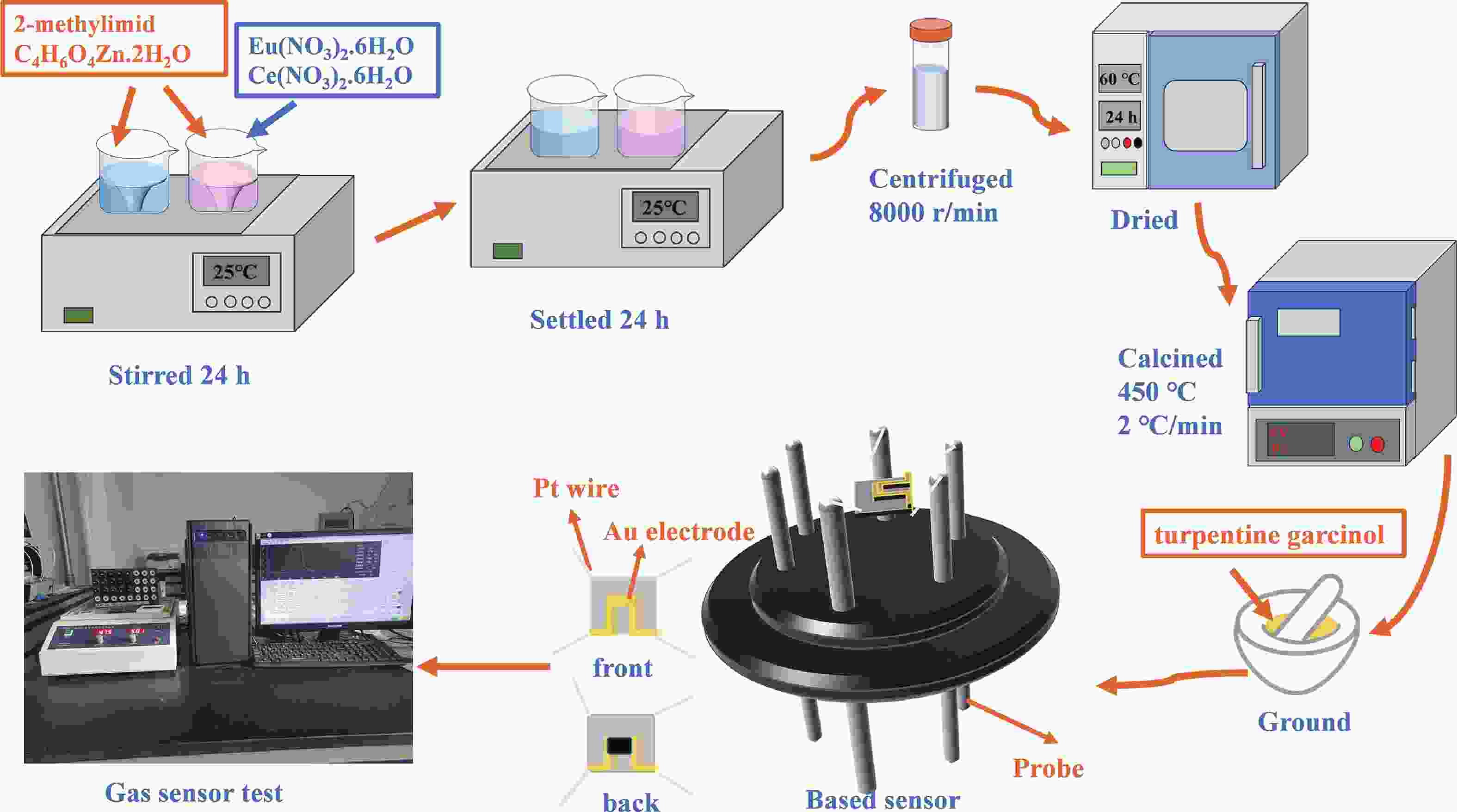
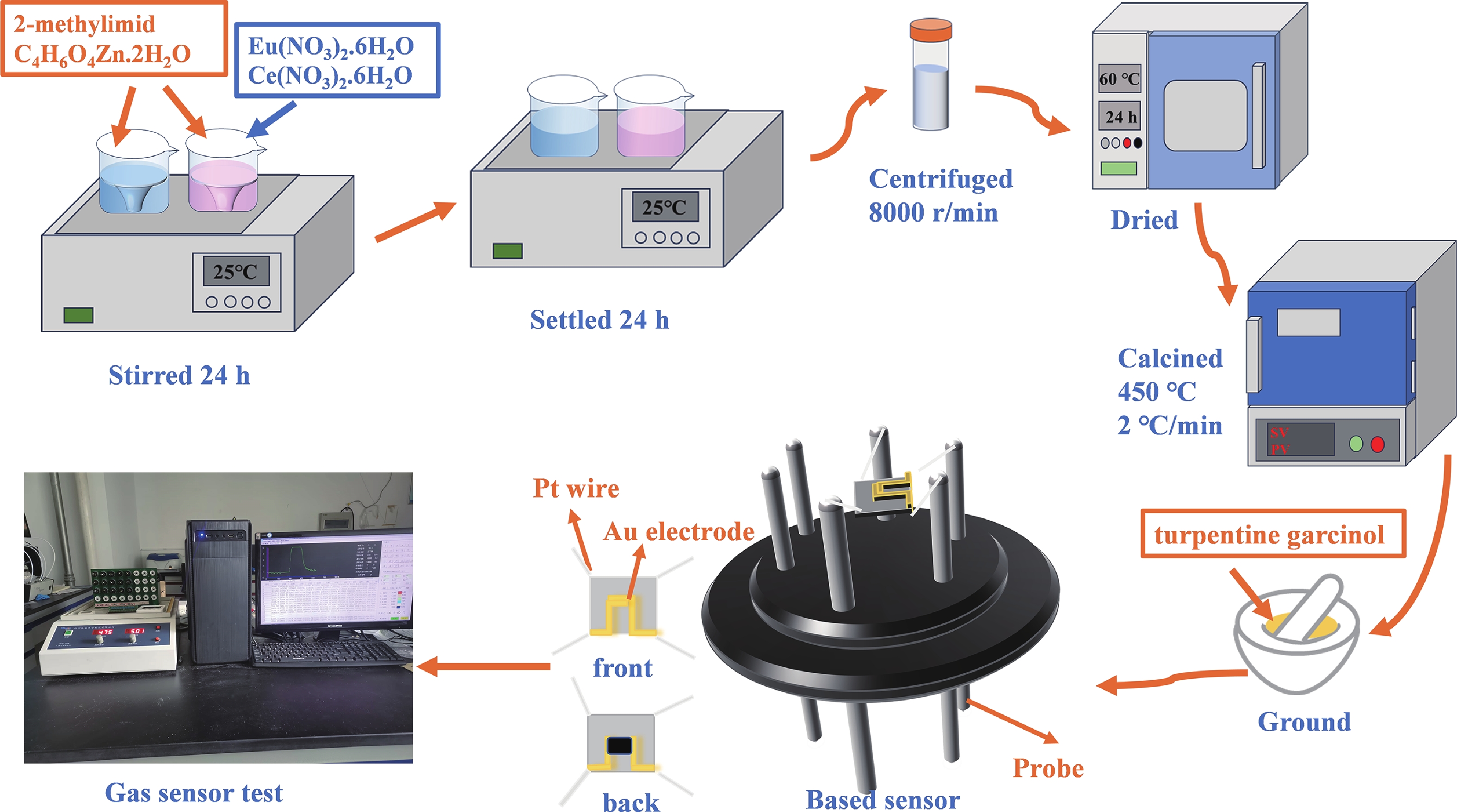
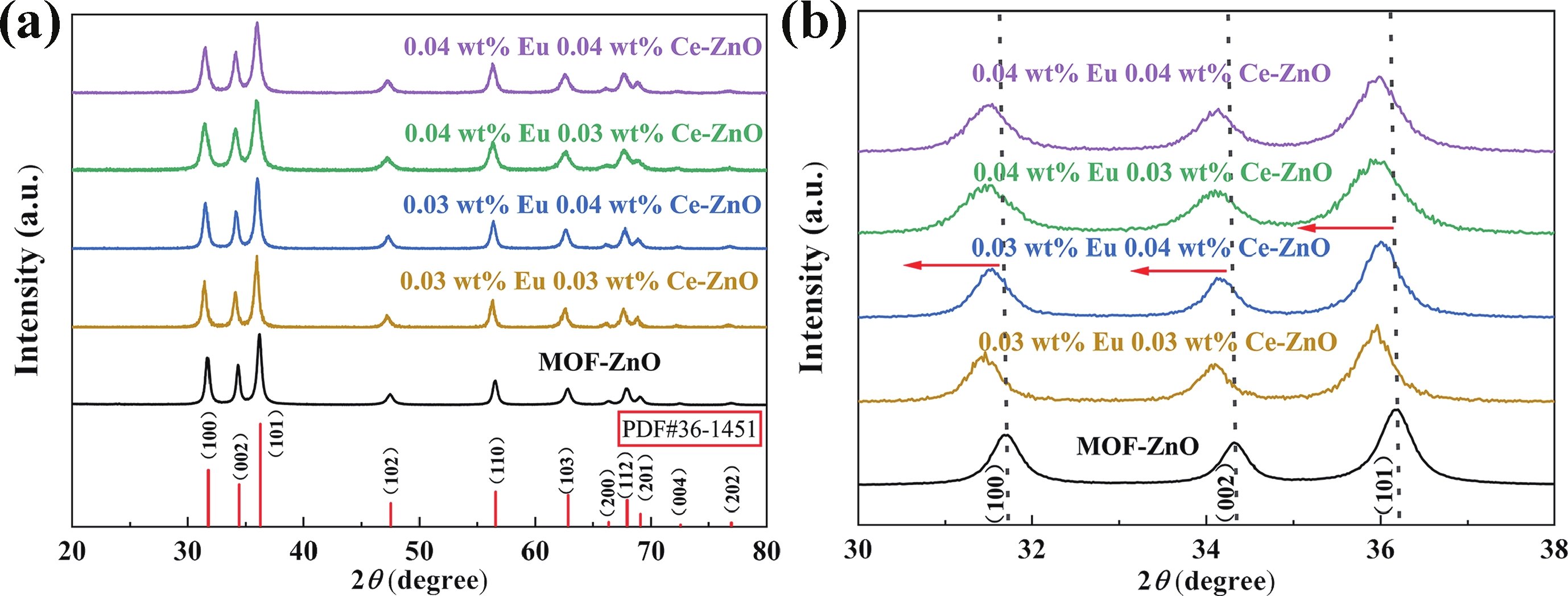
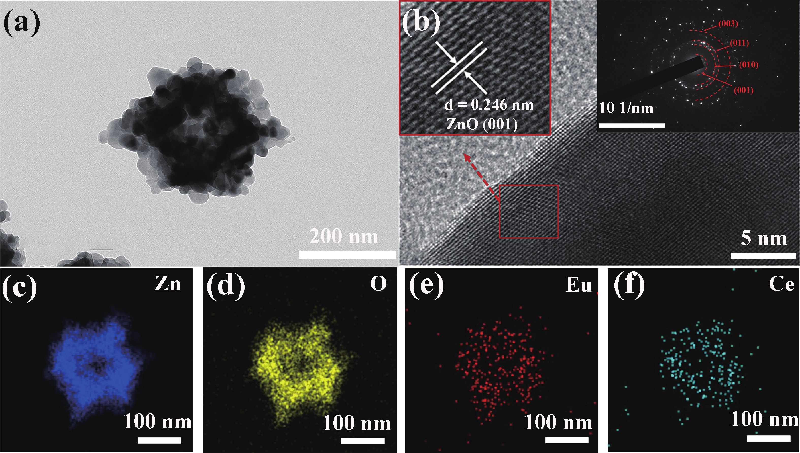
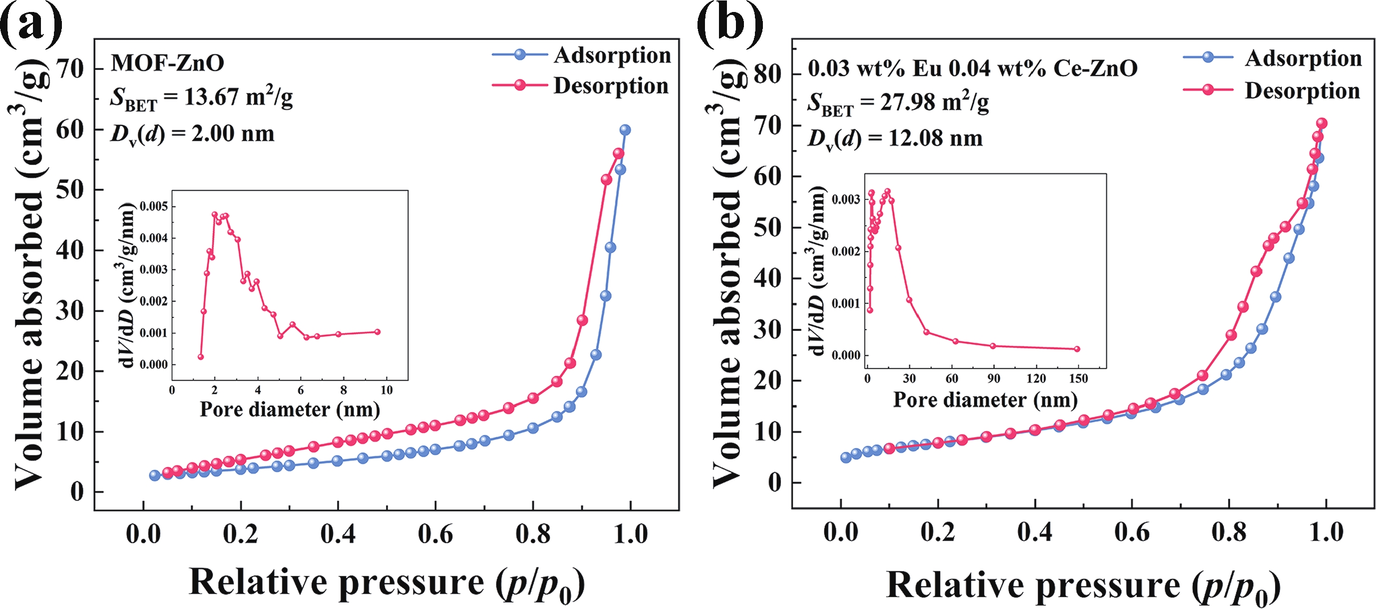
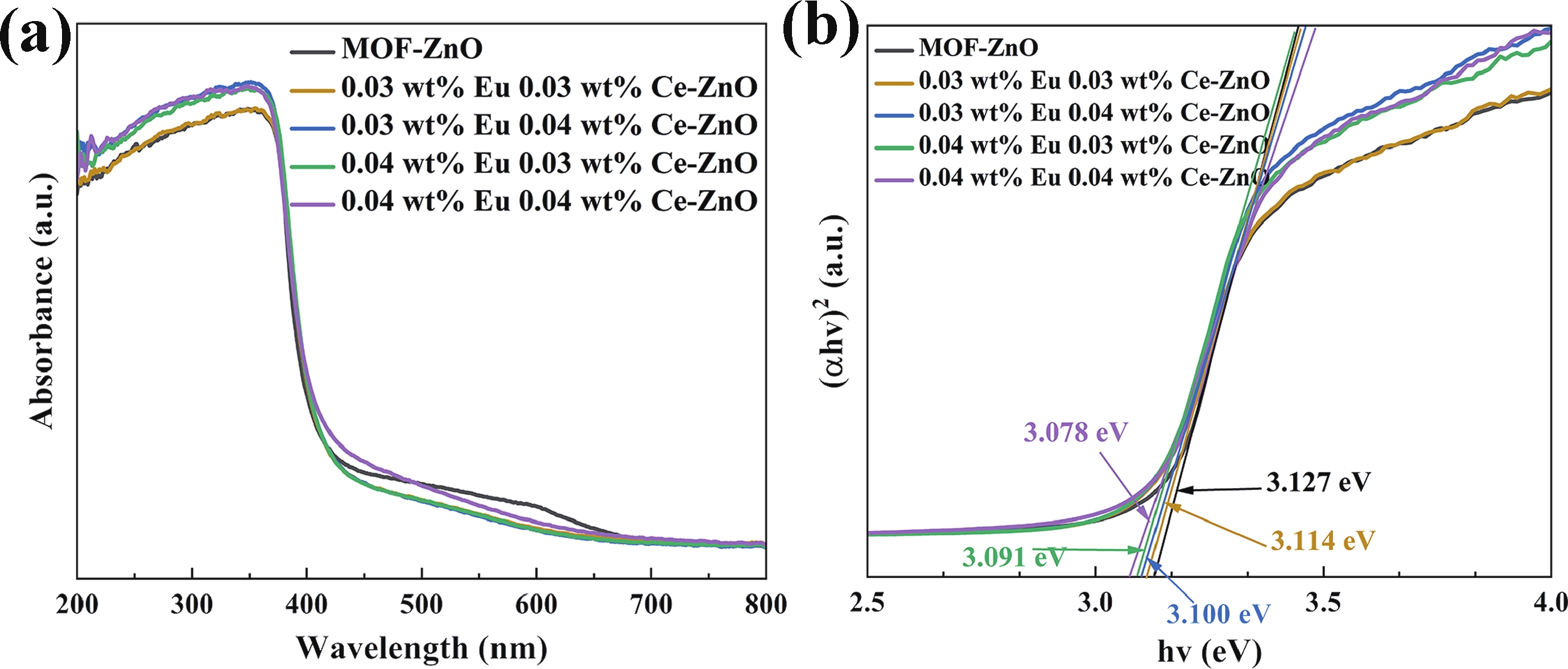
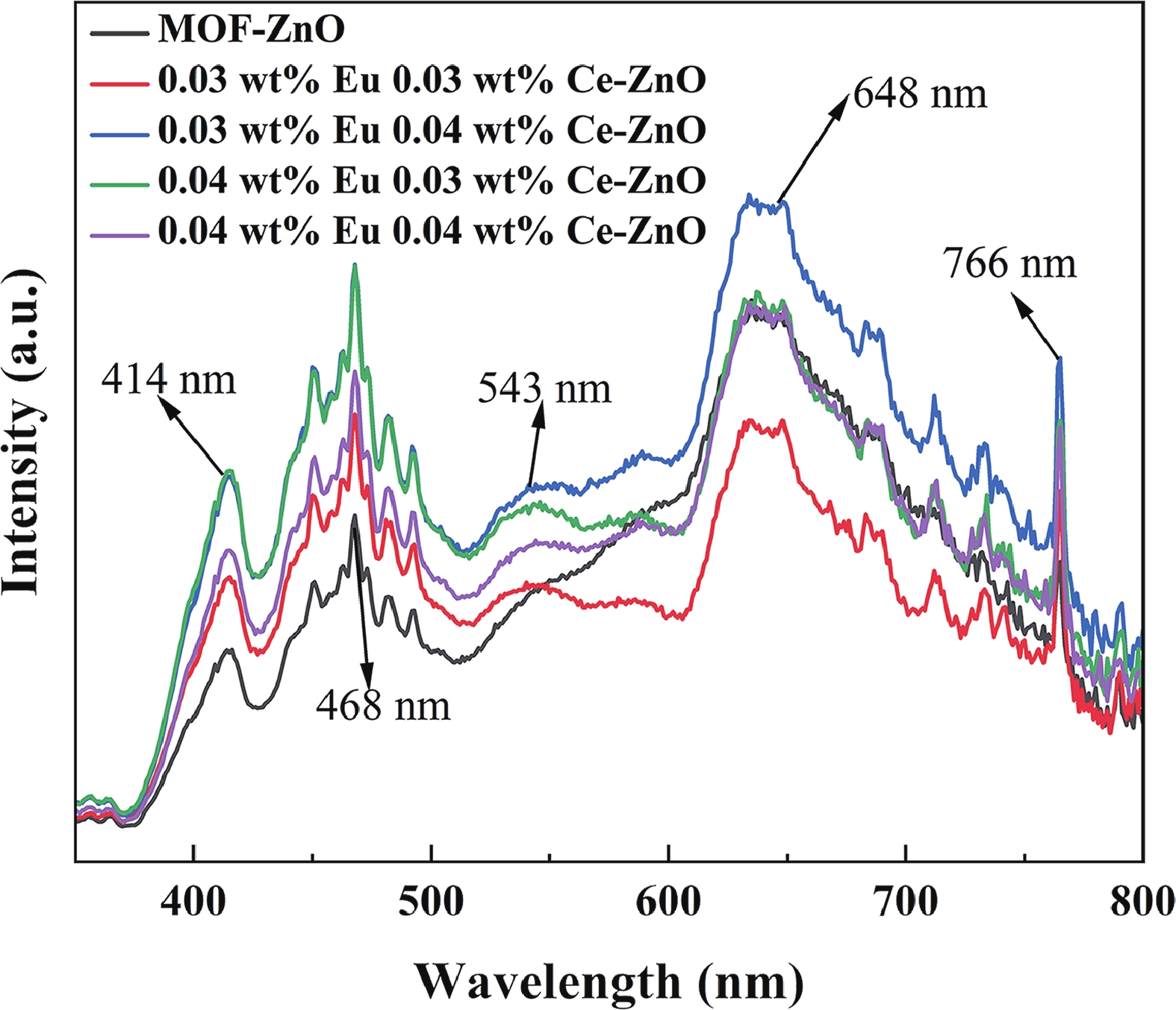
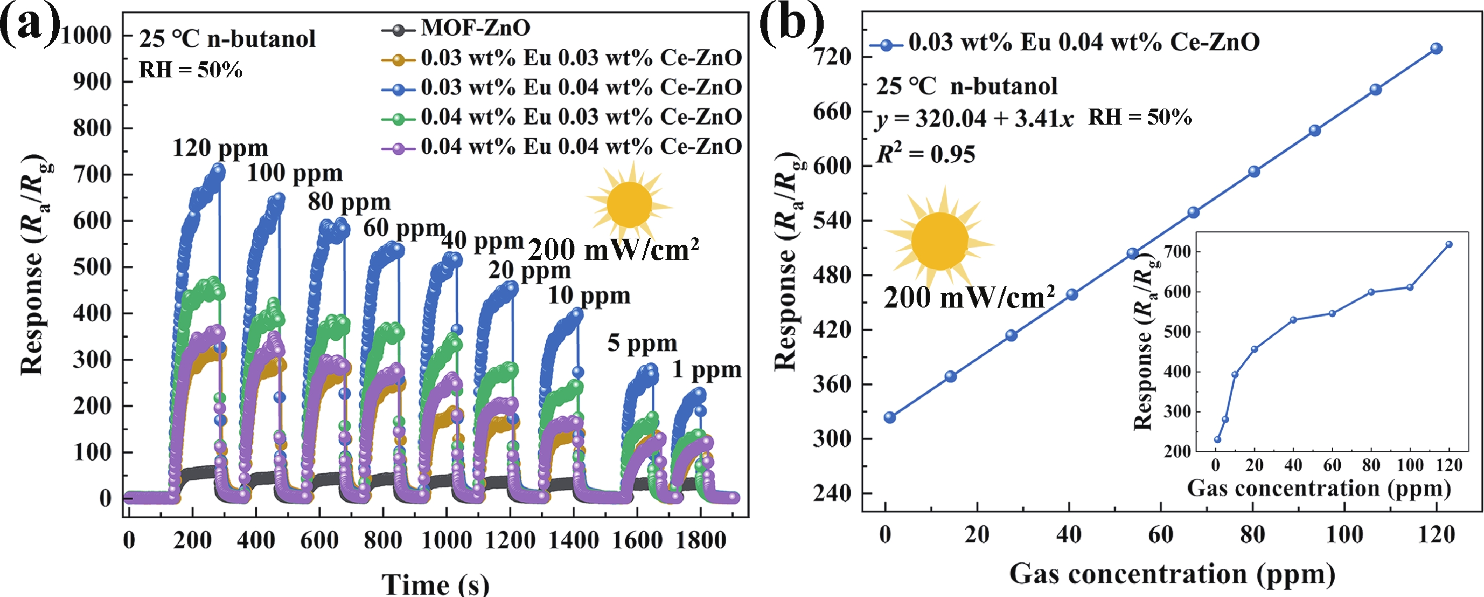
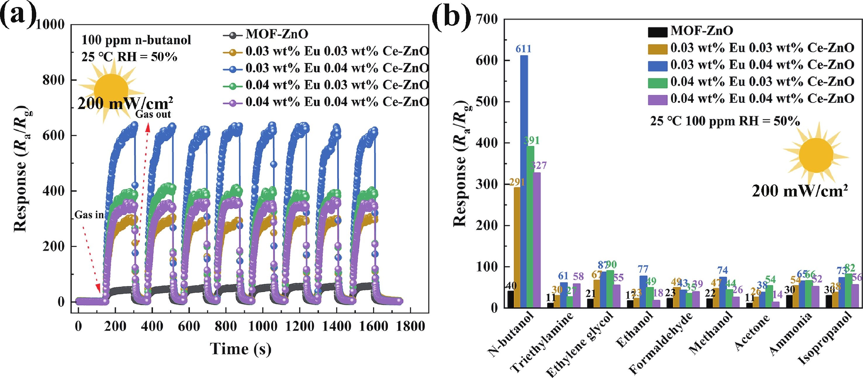
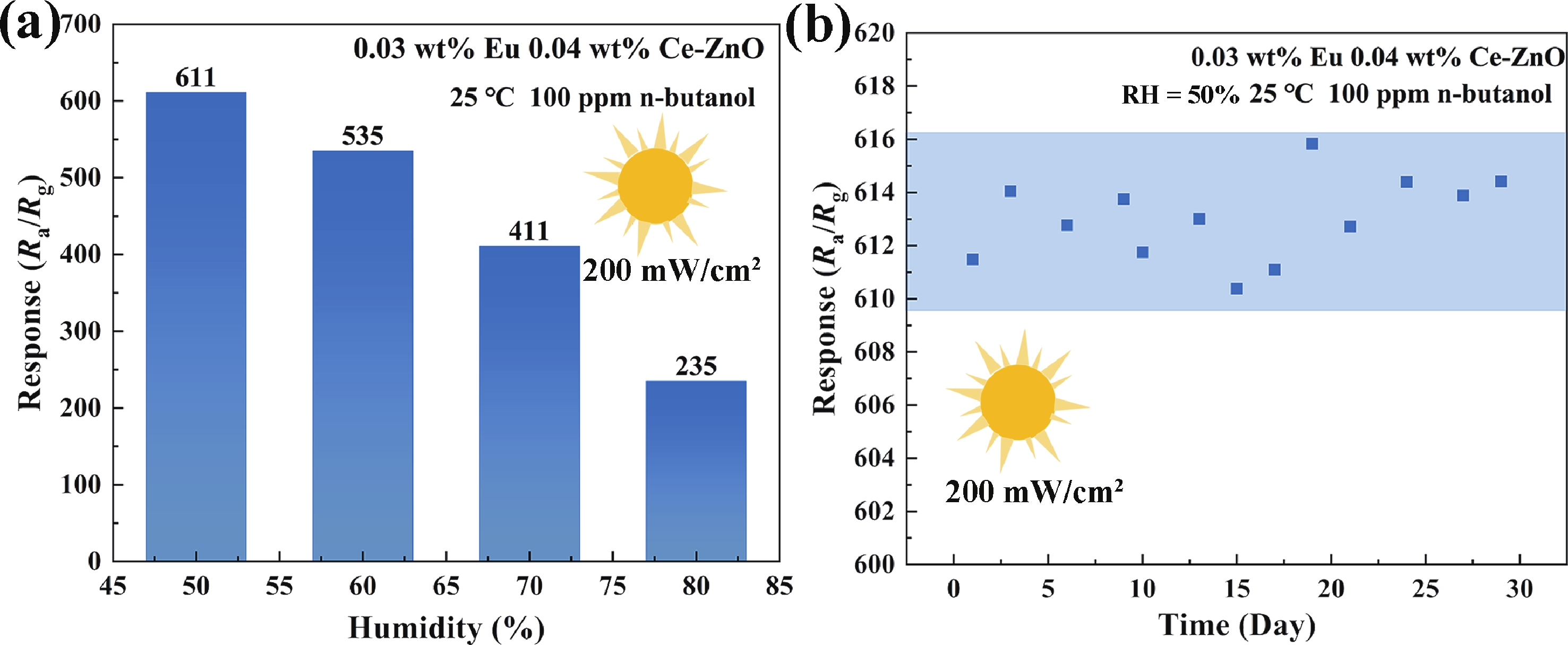
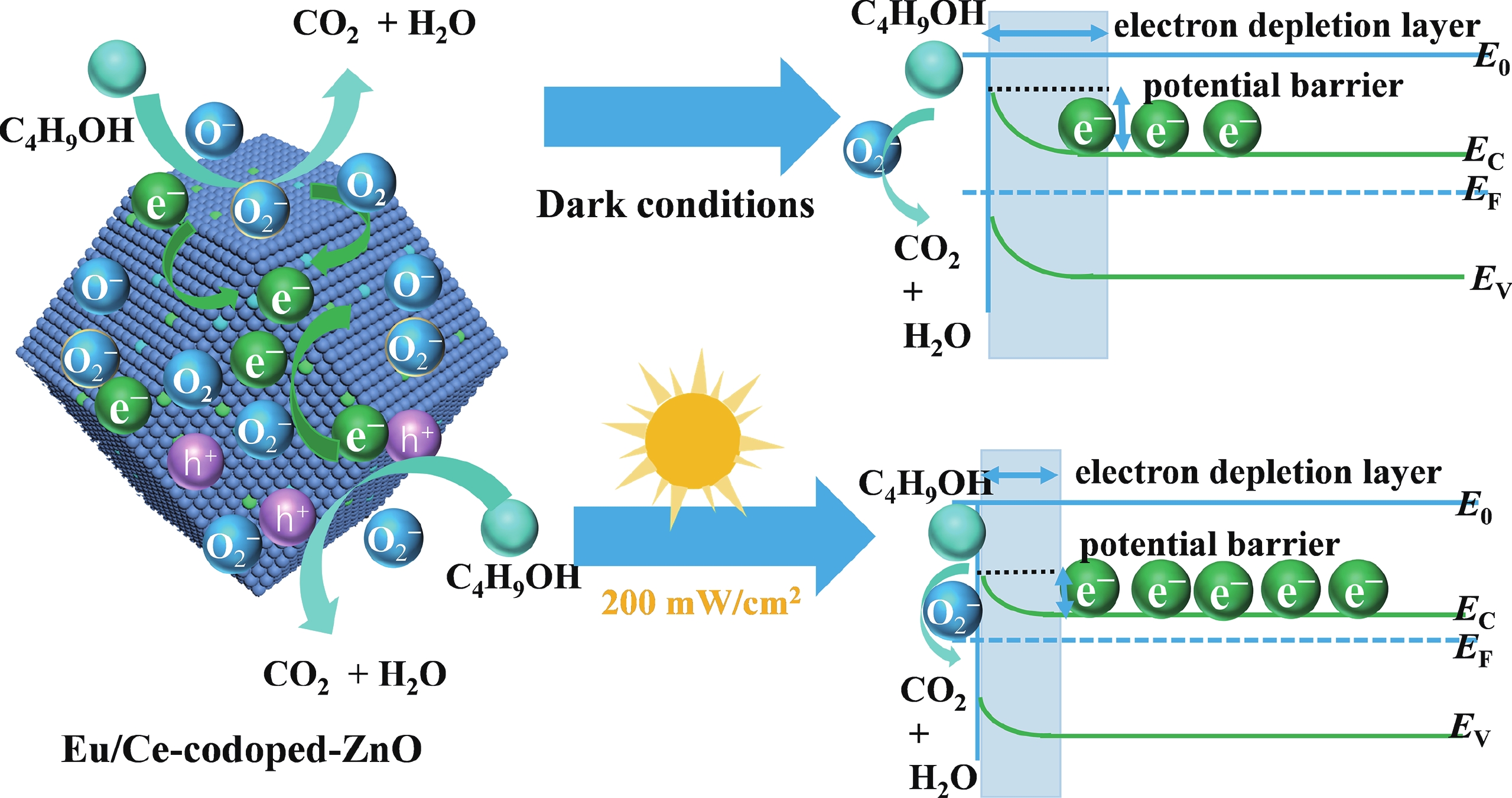
Prolonged exposure to n-butanol, a common hazardous volatile organic compound (VOC) in the environment, can lead to a broad range of adverse health effects. Therefore, detecting n-butanol safely and efficiently at low concentrations becomes critical for both environmental monitoring and human health. In this study, a novel Eu/Ce-codoped MOF-ZnO gas sensor was developed for the sensitive detection of n-butanol gas under ultraviolet activation at ambient temperature. A series of Eu/Ce-ZnO nanomaterials were synthesized via a simple co-precipitation route, by carefully designing the varied mass ratios of Eu and Ce incorporated into pristine ZnO derived from MOF precursors. The gas testing results revealed that introducing an appropriate amount of Eu and Ce would enlarge the specific surface area and enrich the oxygen vacancy content compared to pristine MOF-ZnO. Upon UV irradiation, the 0.03 wt% Eu 0.04 wt% Ce-ZnO sensor achieved a superior response of 611 for 100 ppm n-butanol at room temperature, 15.28 times higher than that of pristine MOF-ZnO (40). Furthermore, the sensor presented rapid response/recovery times (15 s/28 s) and excellent selectivity. The above contributions pave the way for the promising development of highly sensitive, ultraviolet-enhanced gas sensors for ambient temperature detection of VOCs.


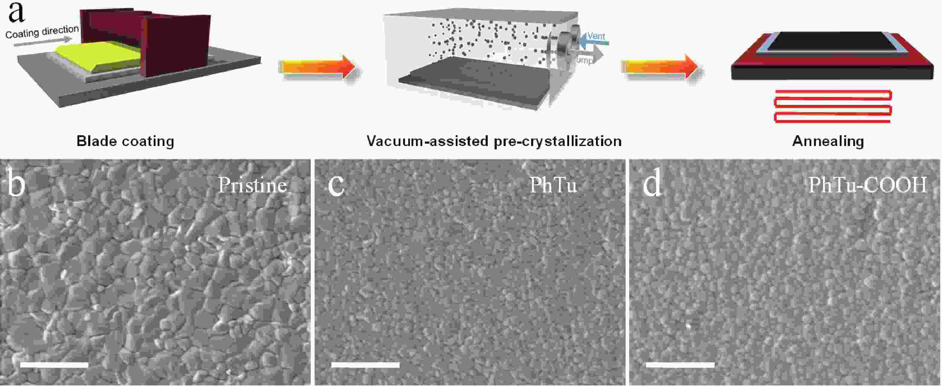
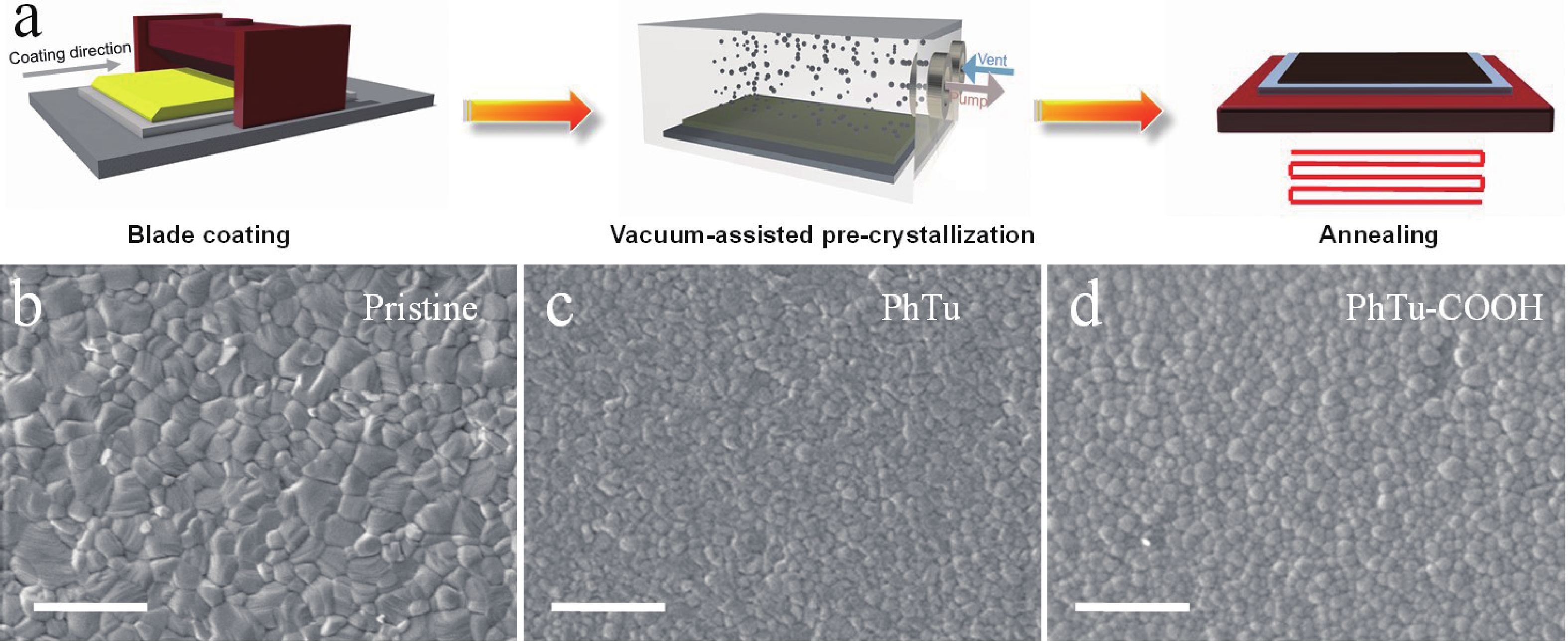
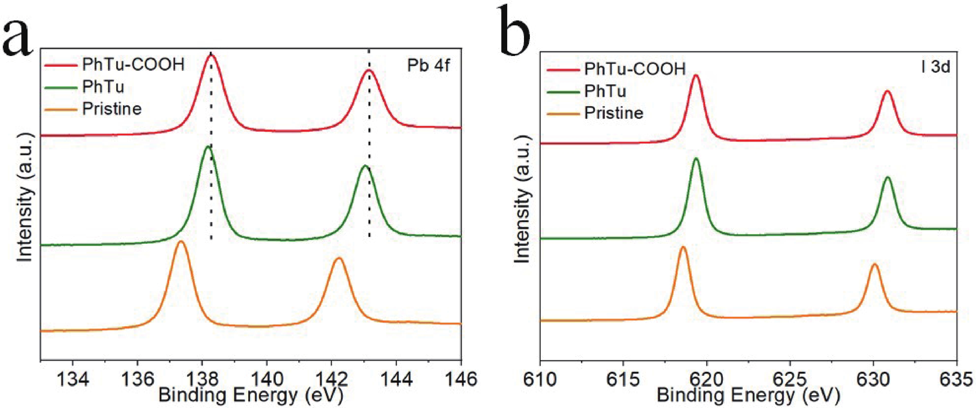
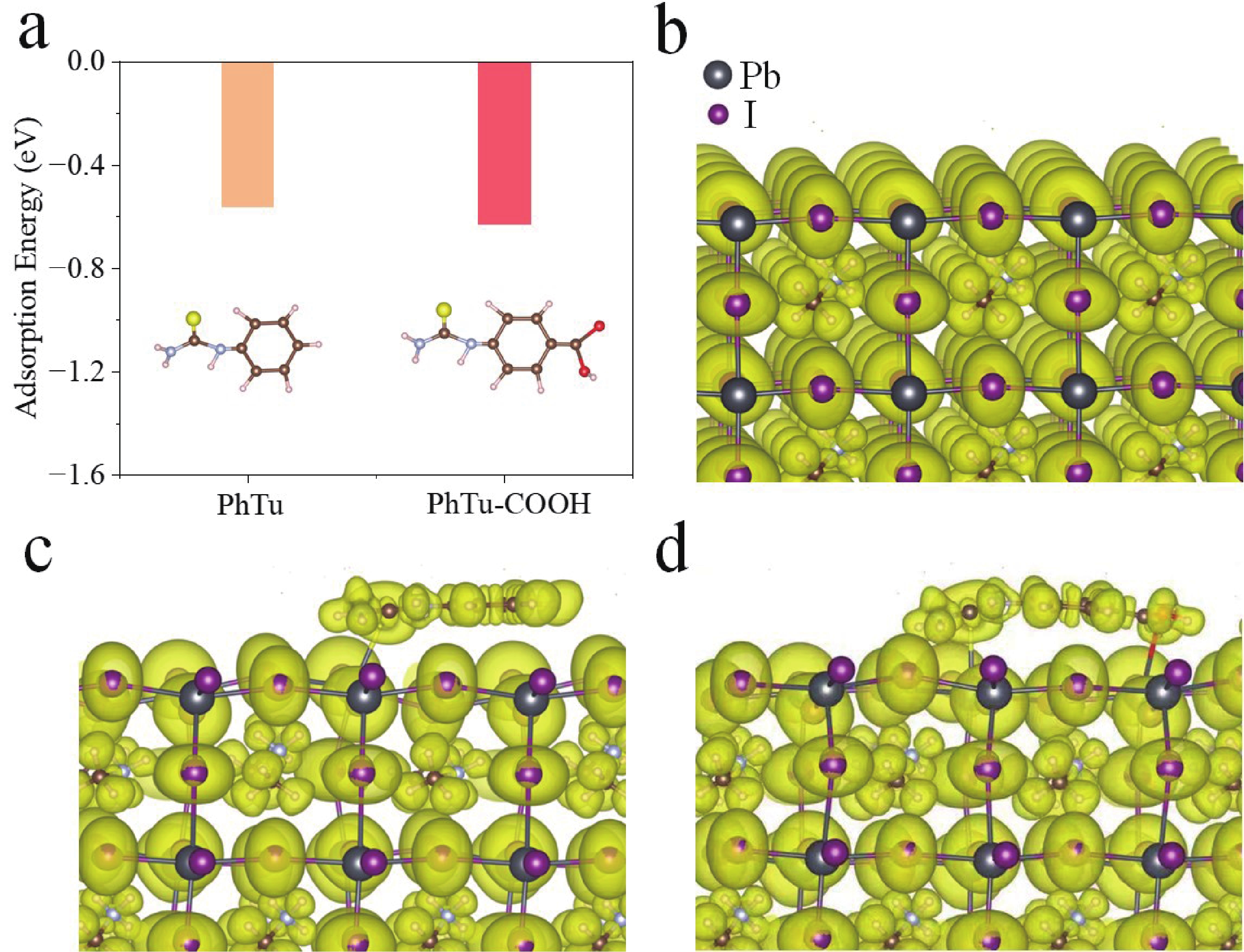
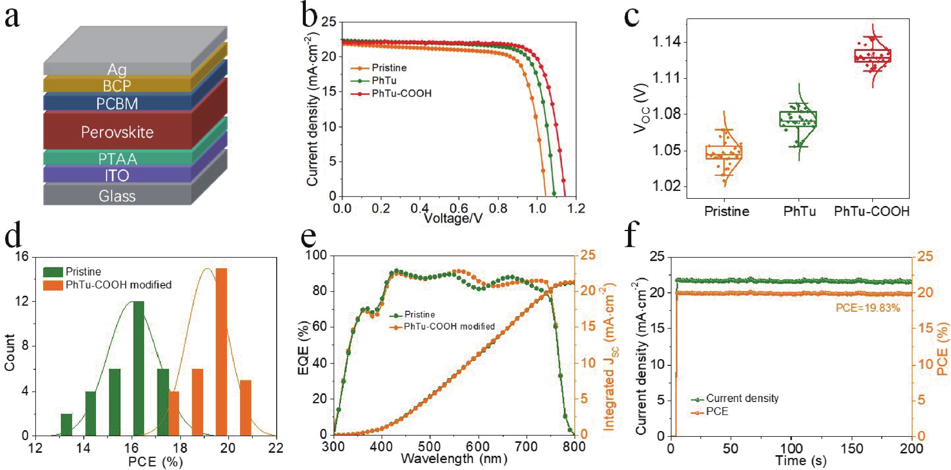
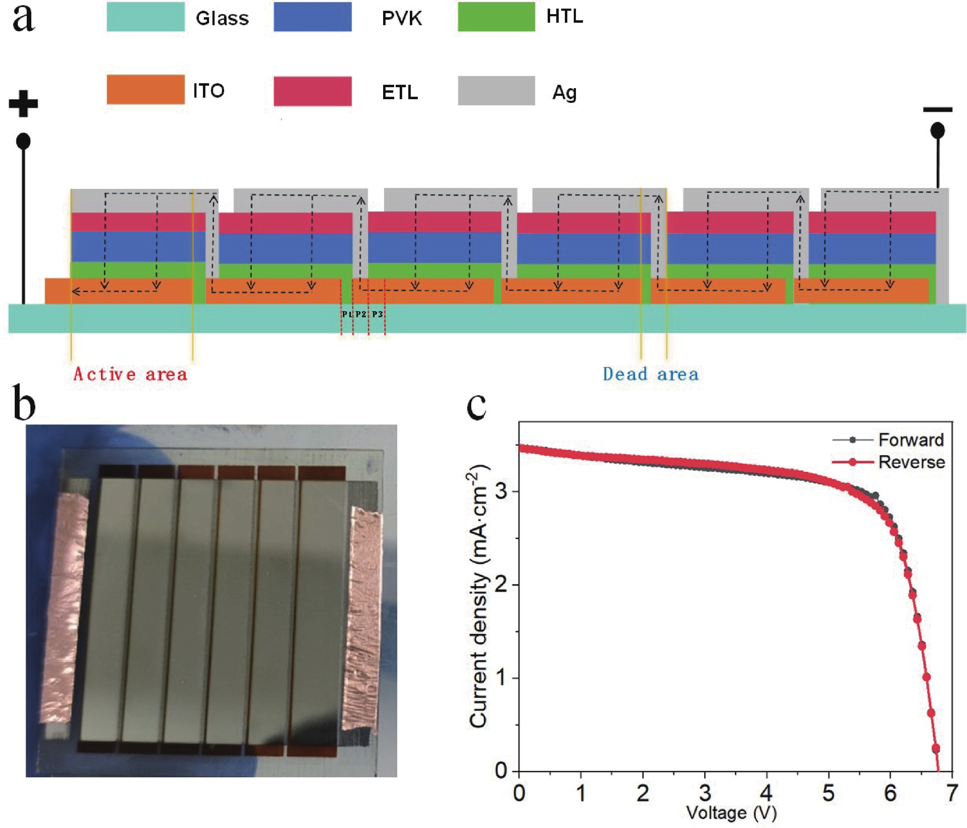
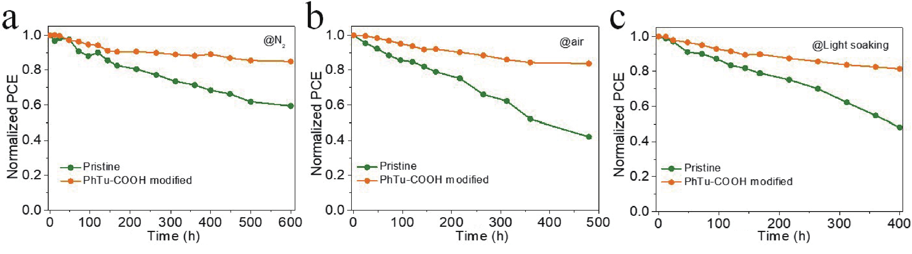
Although the certified power conversion efficiency (PCE) of single-junction perovskite solar cells (PSCs) has achieved a high level of 27%, approaching the single-crystalline silicon solar cells, the device stability remains an urgent issue to be resolved for the commercialization. Defect passivation emerged as a viable approach to enhance the operational stability of the solar devices. Herein, phenylthiourea (PhTu) derivatives are selected as effective passivation agents to enhance the optoelectronic properties of printed methylammonium lead iodide (MAPbI3) films. It is demonstrated that incorporating a small amount of 1-(4-carboxyphenyl)-2-thiourea (PhTu-COOH) significantly reduces the trap-state density and leads to longer carrier lifetime of the perovskite films. As a result, the inverted solar device made of PhTu-COOH-modified MAPbI3 perovskite film shows remarkably improved efficiency (from 17.29% to 20.22%) and obviously increased open-circuit voltage (VOC) (from 1.043 to 1.143 V), as compared with the pristine device. Moreover, the PhTu-COOH-modified PSCs exhibit enhanced operational stability due to the significantly reduced trap-state density. Finally, the optimized solar module fabricated with an active area of 11.28 cm2 delivers a high PCE of 17.07% with negligible VOC loss, demonstrating the feasibility of the blade-coating method for large-area perovskite film deposition.

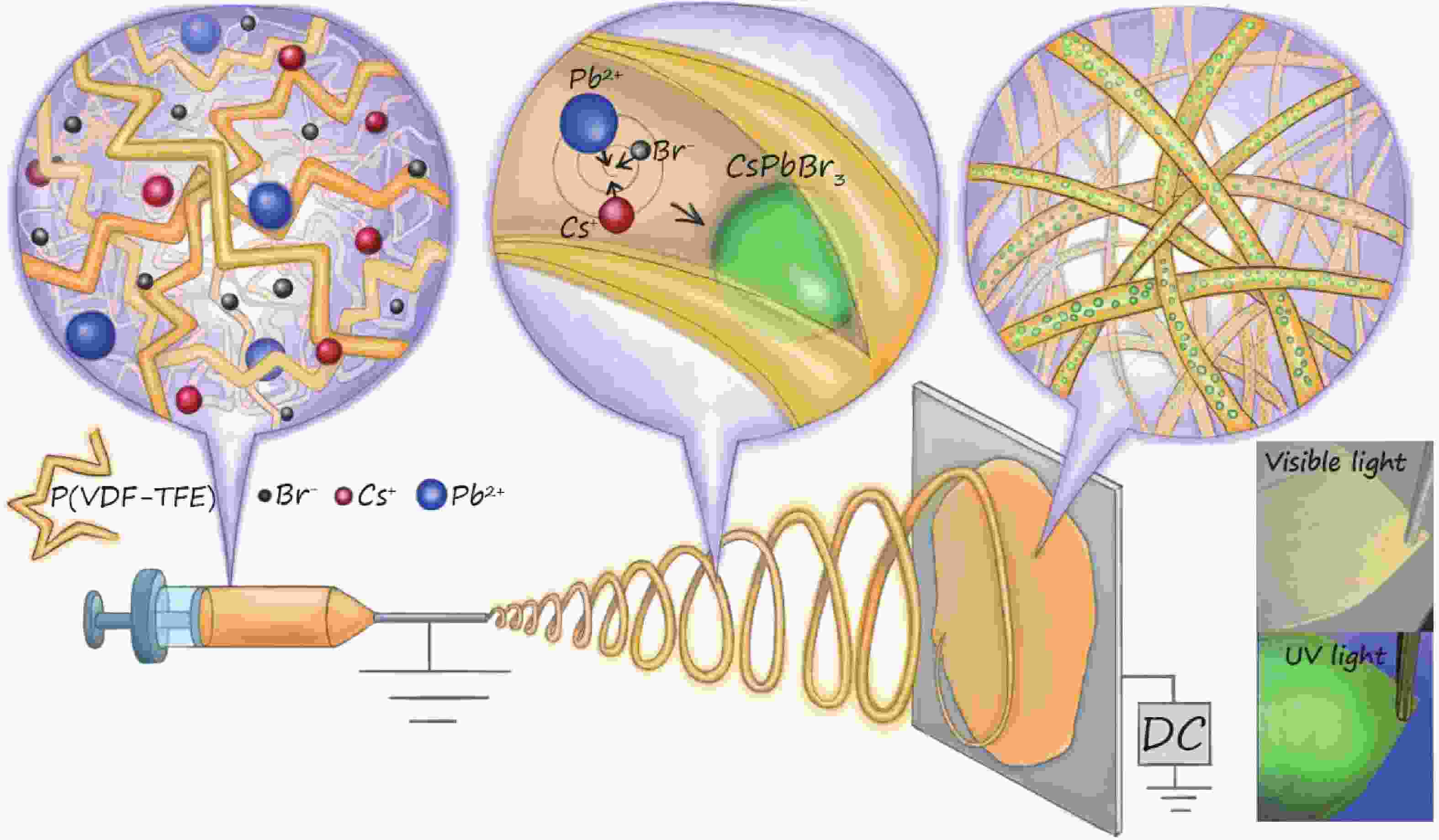
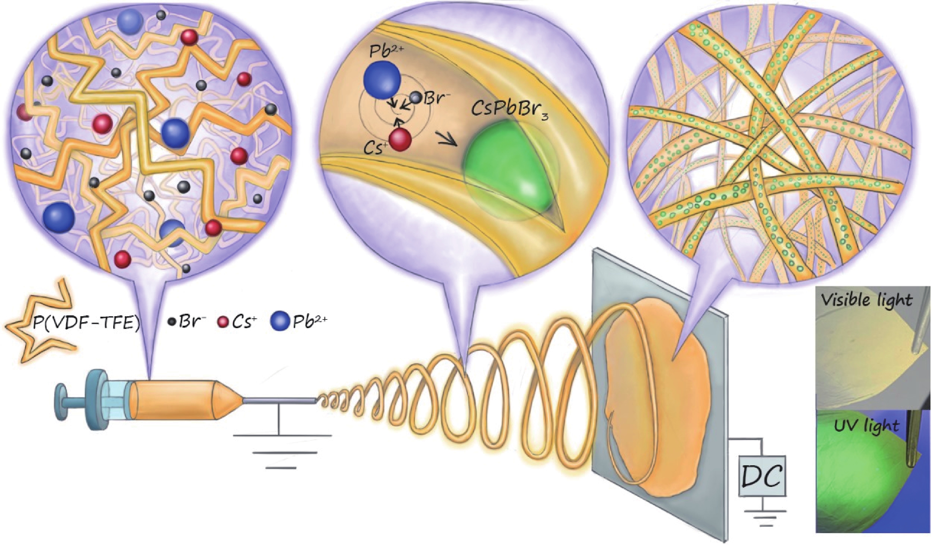
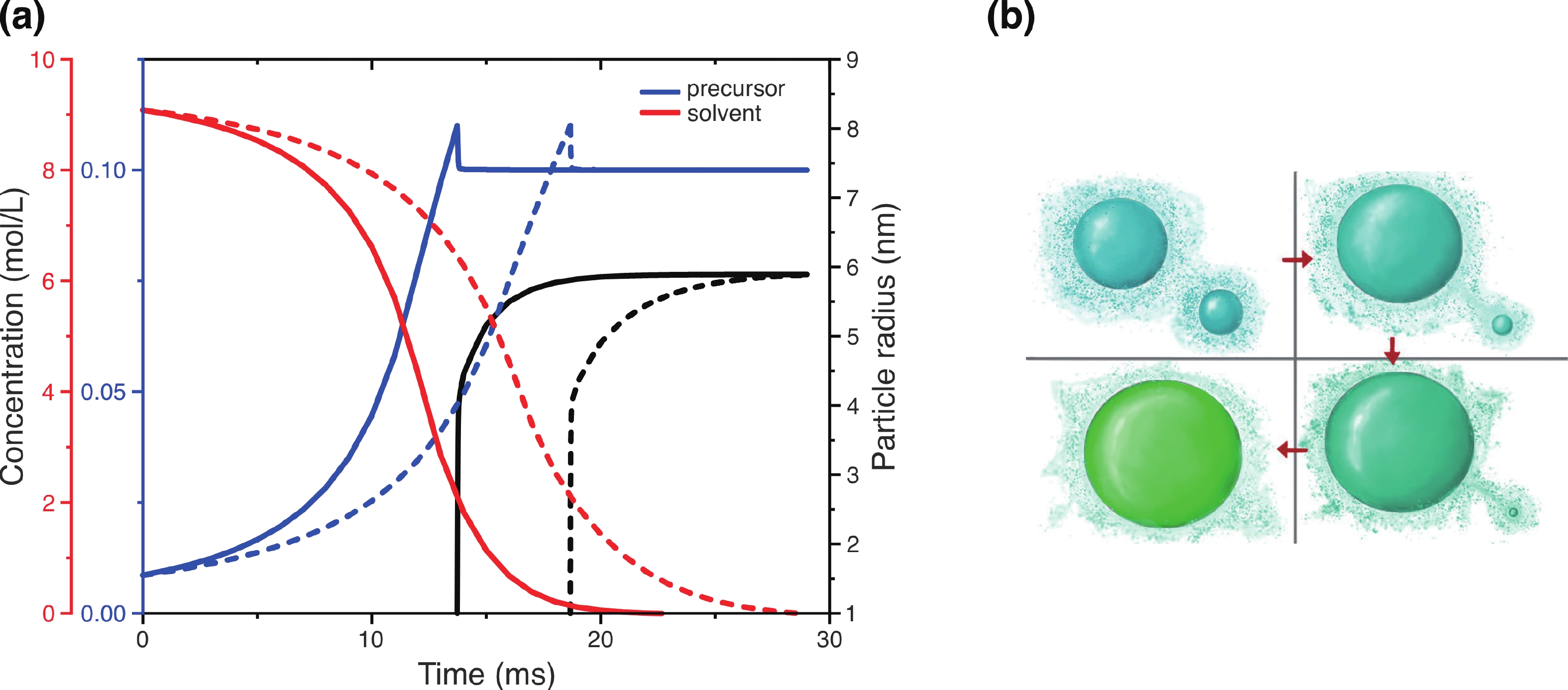
Flexible materials with perovskite quantum dots (PQDs) are widely used in the field of photonics and opto-electronics due to their unique properties. Development of new materials based on these nanoparticles, incorporated into flexible and lightweight nonwoven fabrics, demonstrated high photoconductivity and efficient light energy conversion. In this work, we propose a method for creating a stable luminescent nonwoven material using electrospinning, in which inorganic salt precursors are used without the need for additional stabilizers. Equimolar solutions of cesium and lead (Ⅱ) bromide were mixed with a fluoroplast, resulting in a series of samples. Luminescent materials were obtained containing PQDs with a composition of CsPbBr3, with emission peaks ranging from 507 to 517 nm under 365-nm excitation. We have experimentally established and theoretically confirmed that the peak position is related to the size of the particles formed in the fiber during electrospinning and depends on processing time. Developed materials exhibited stable luminescent properties for up to 2.5 years, making them a promising candidate for the development of new flexible optoelectronic devices based on PQDs.