Issue Browser
Volume 47, Issue 4,
Apr 2026
Column
J. Semicond.
2026, 47(4): 041301 doi: 10.1088/1674-4926/25060003

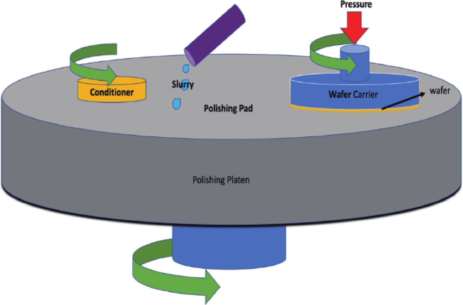
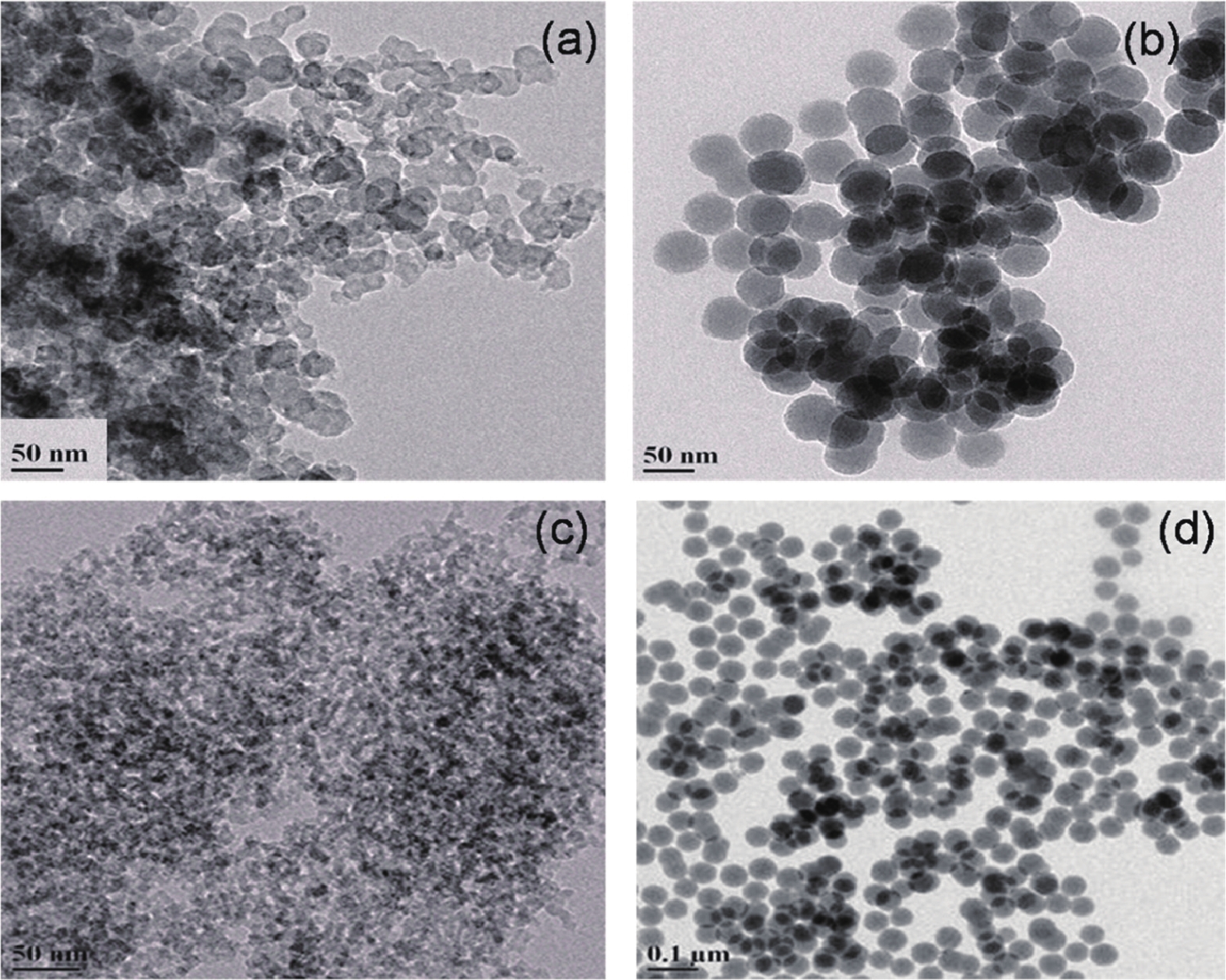
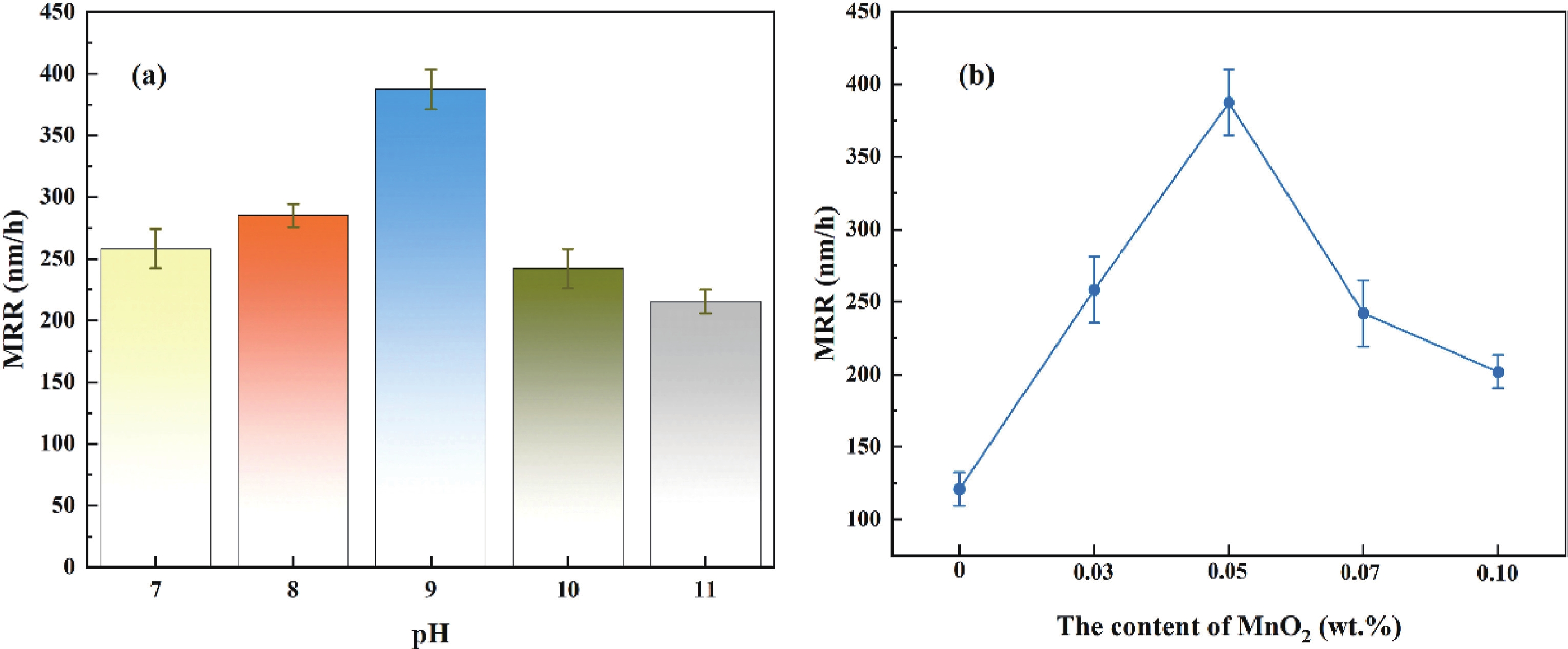
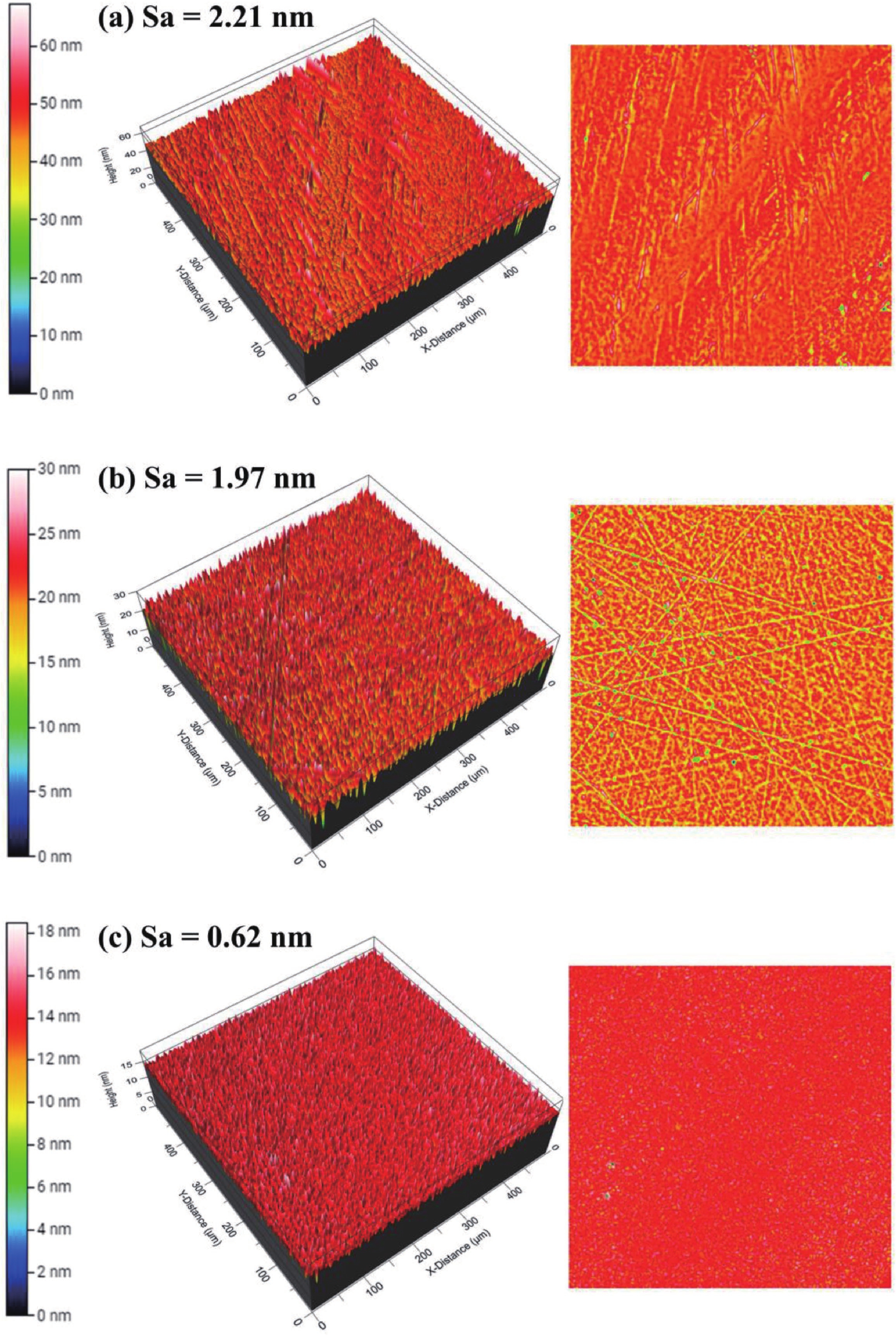
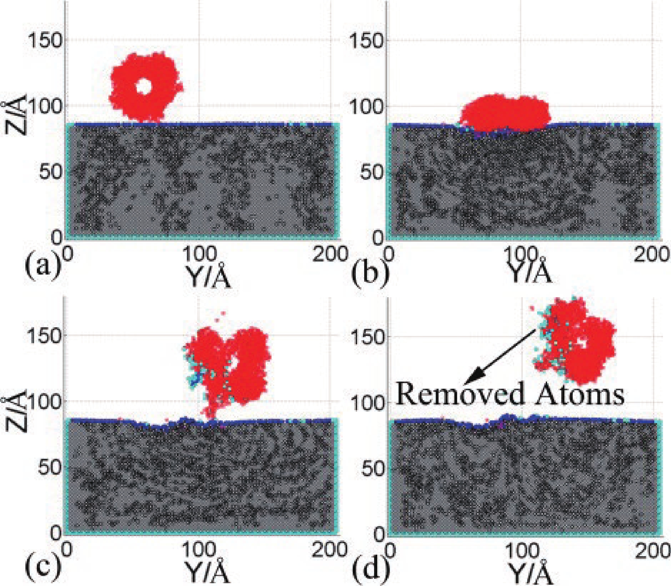
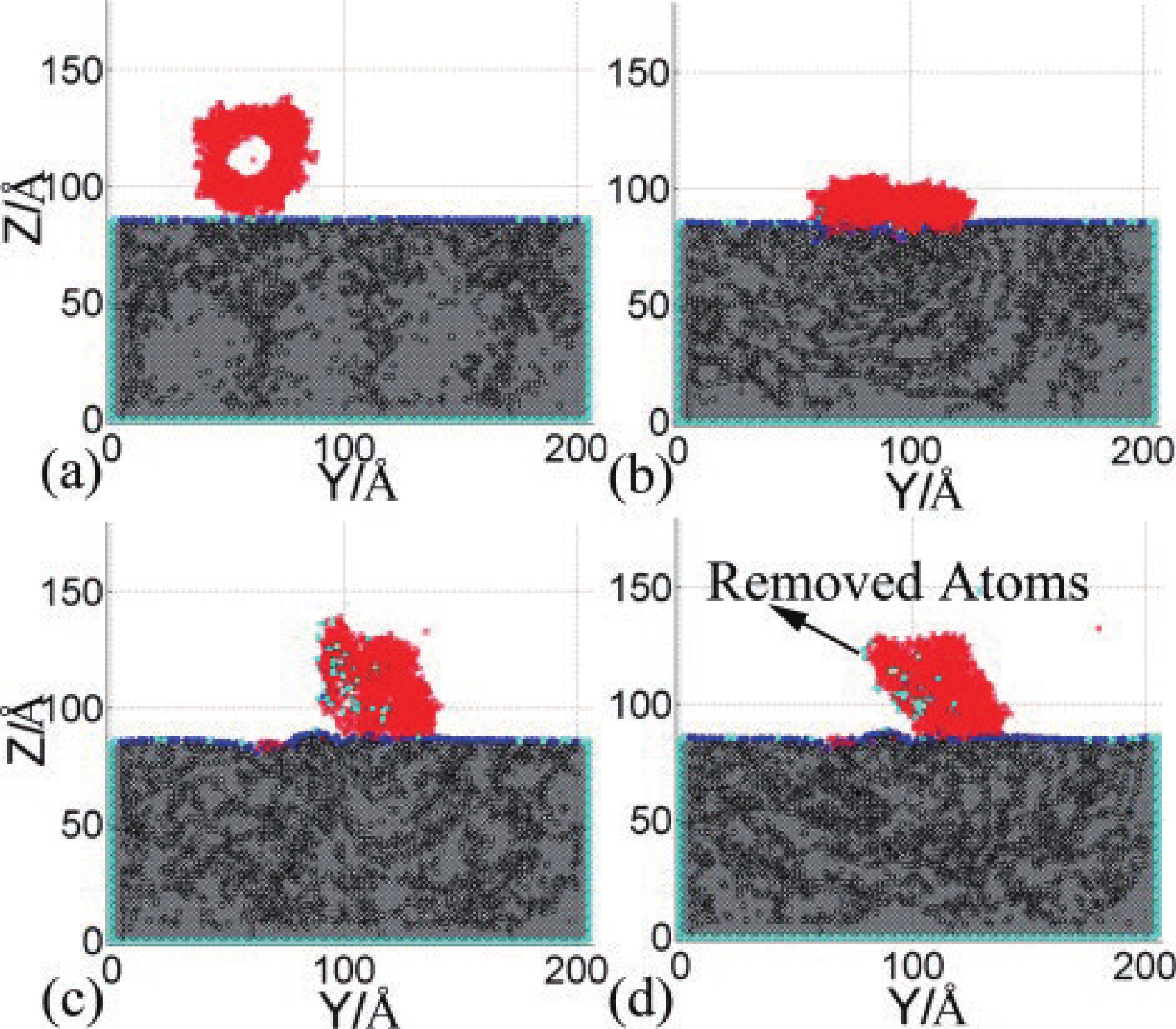
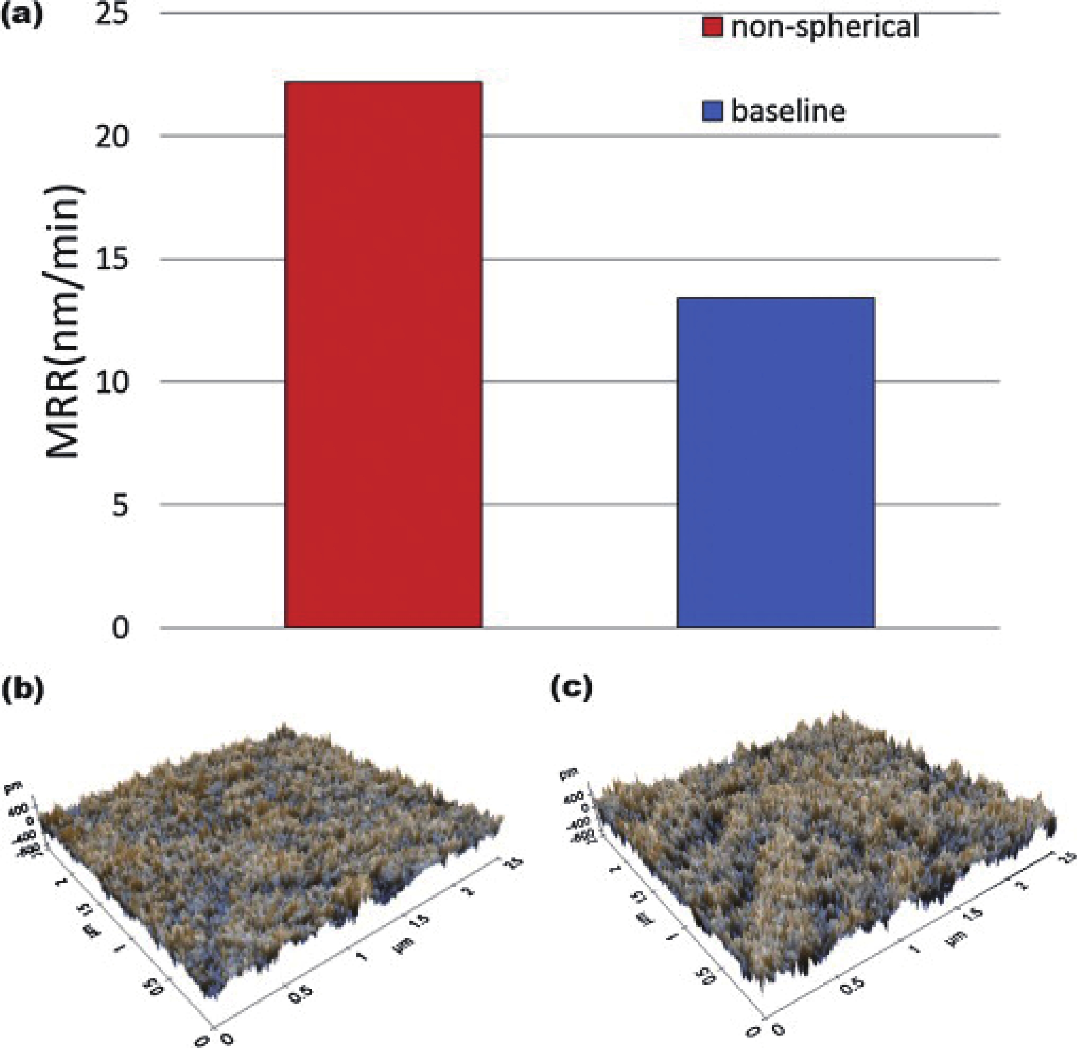
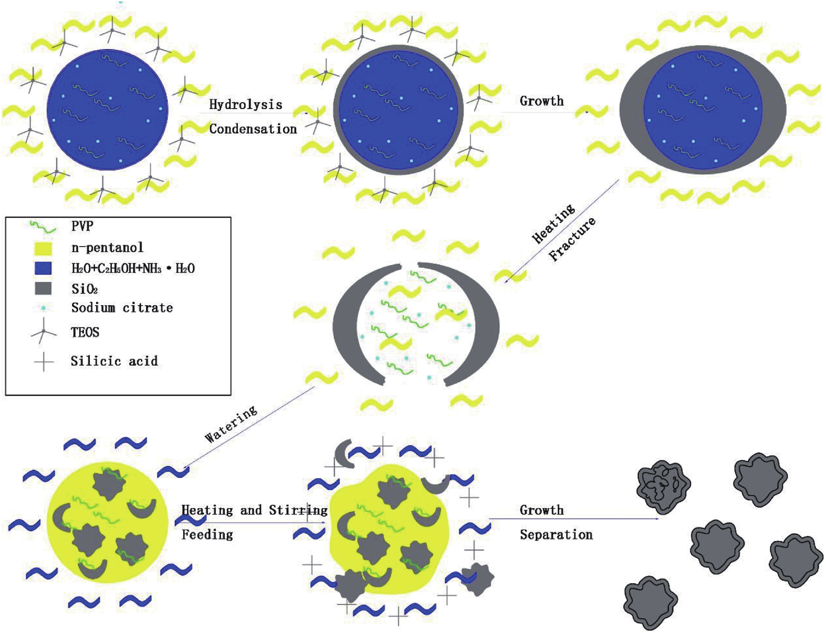
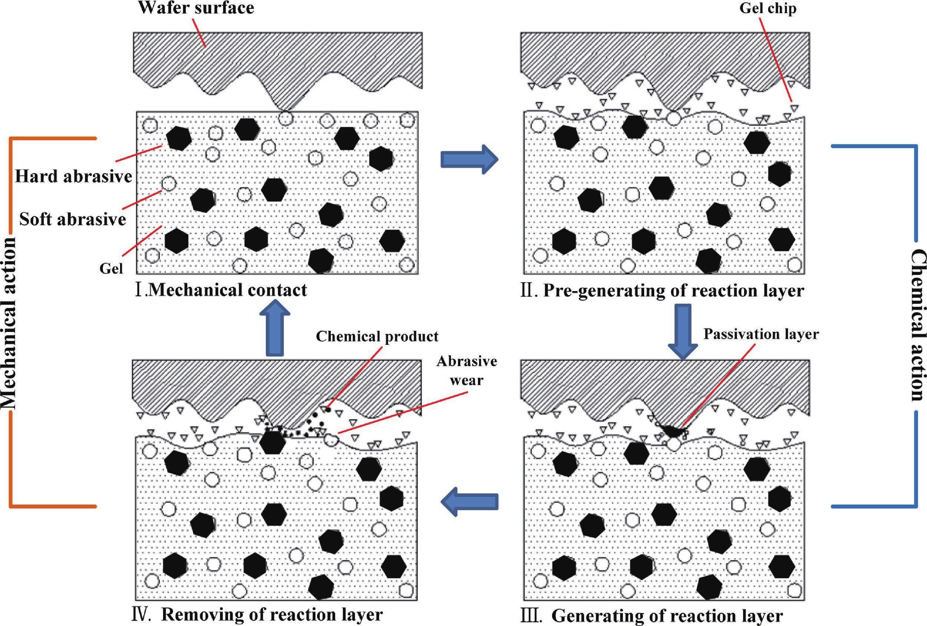
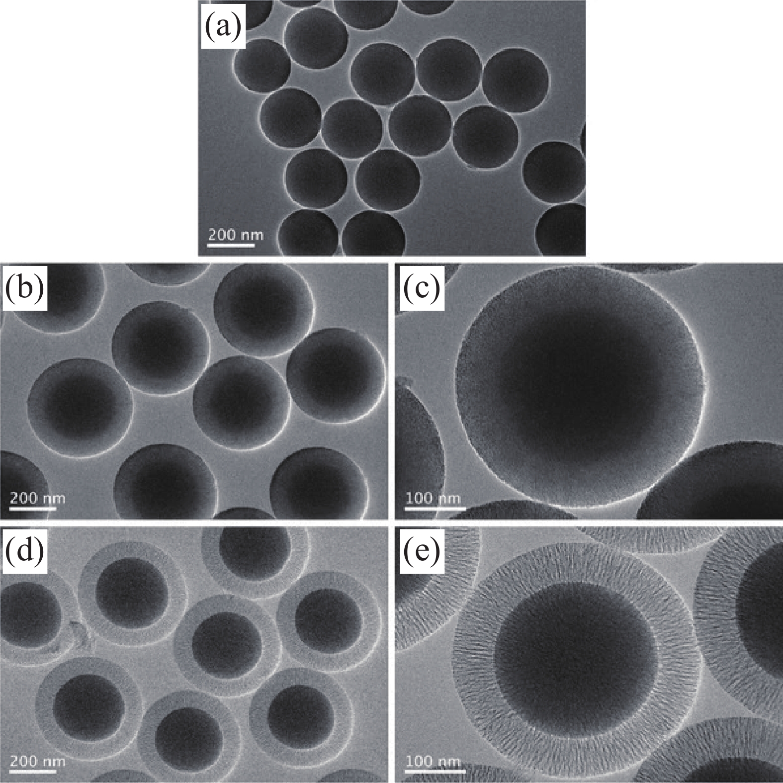
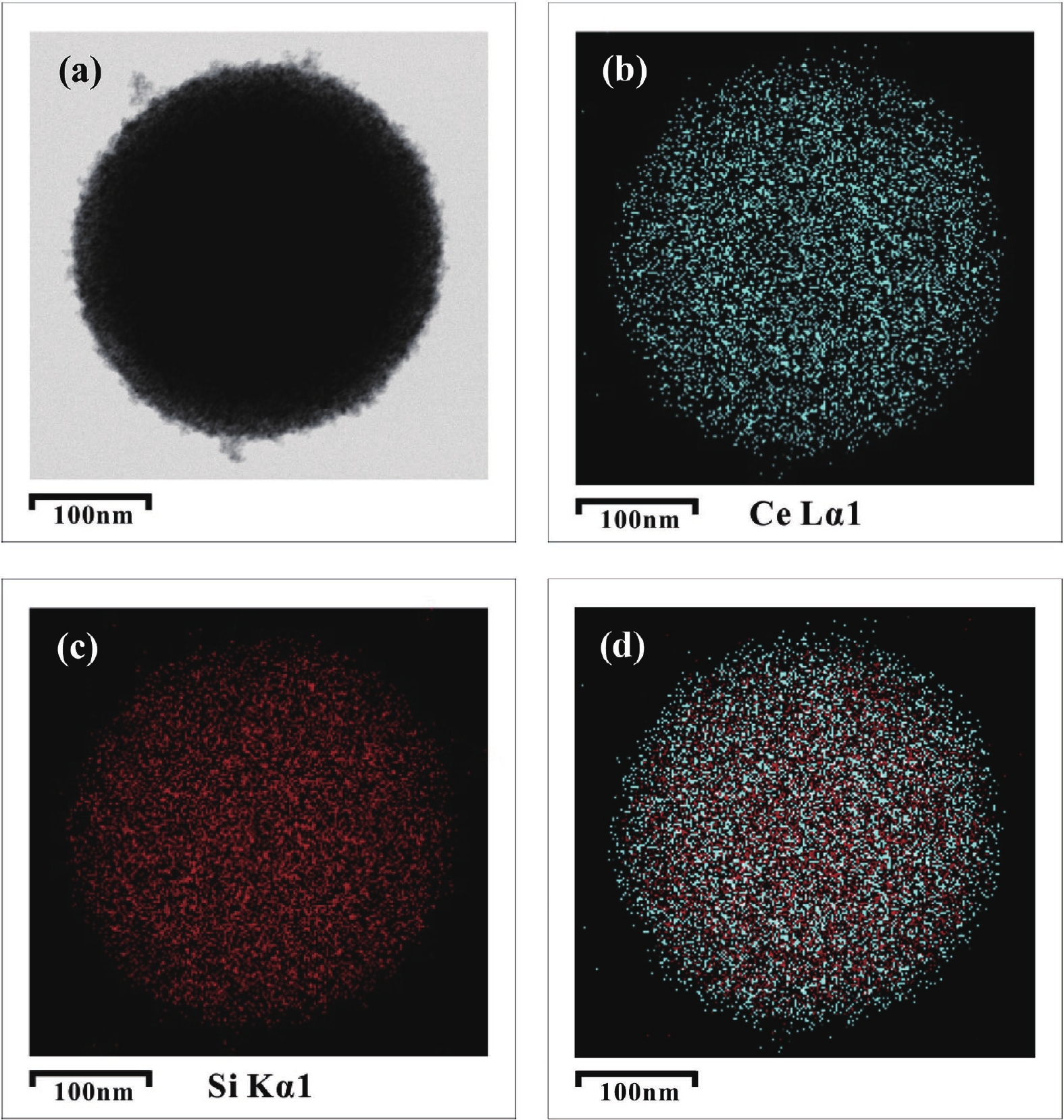
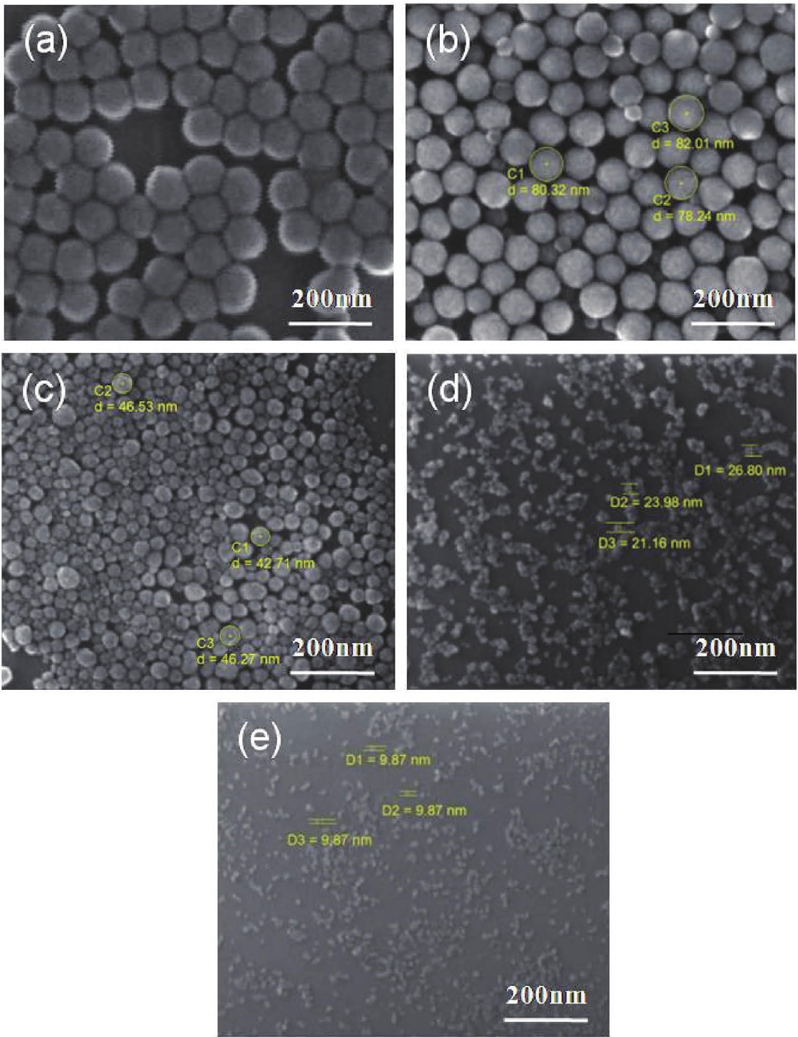
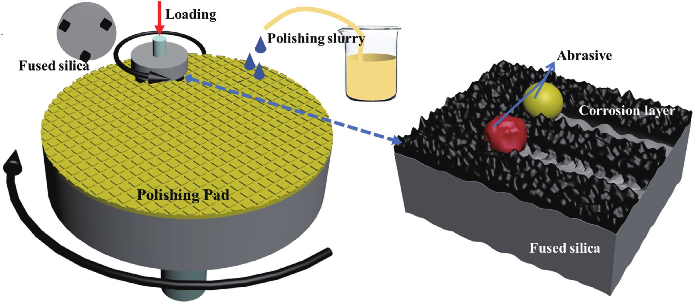
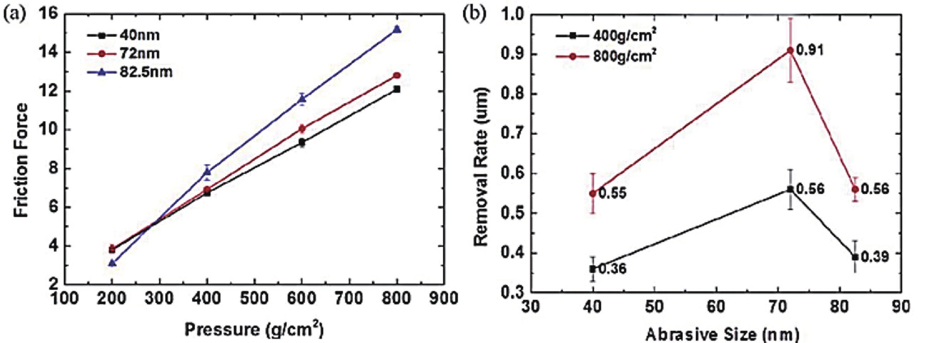
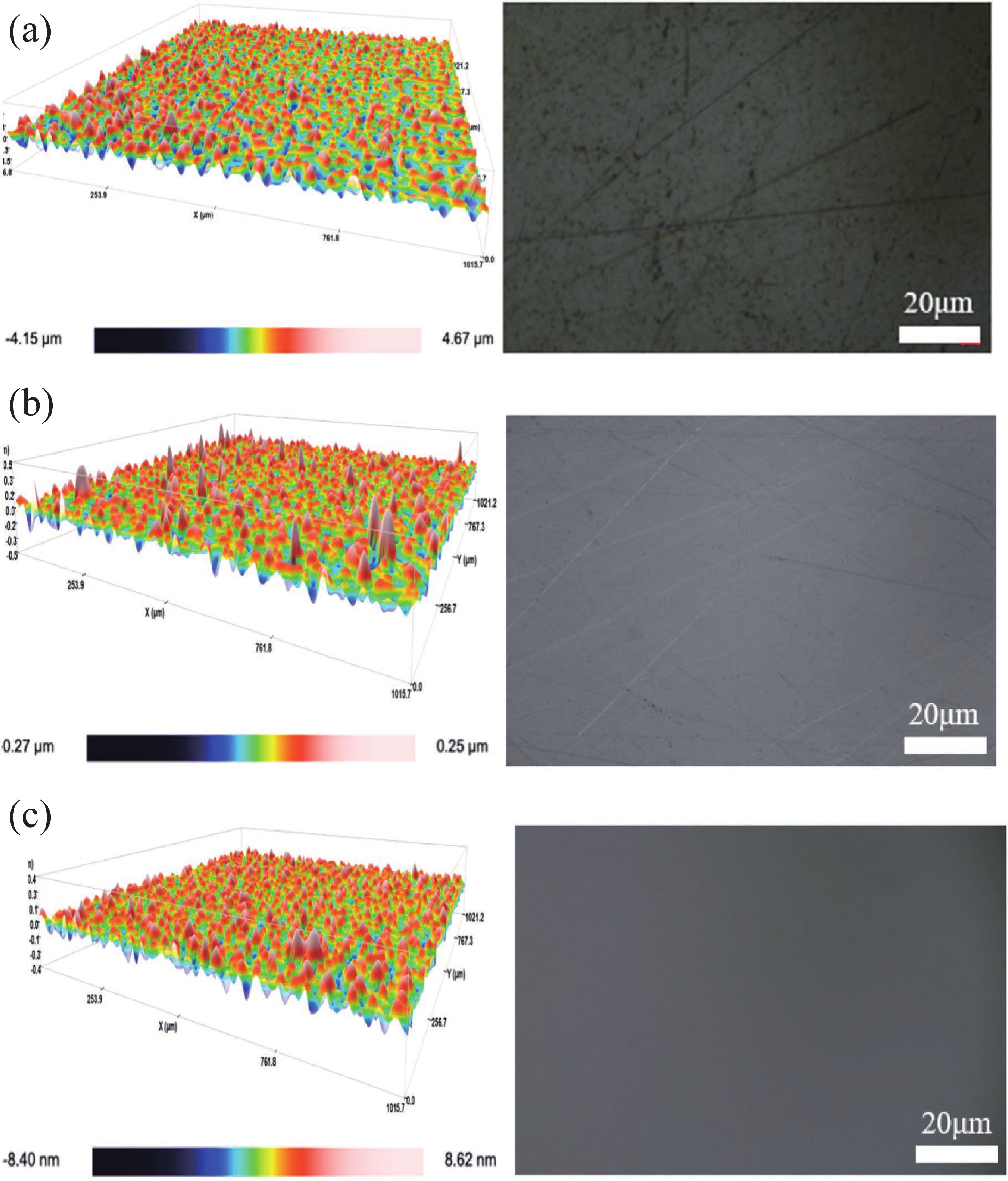
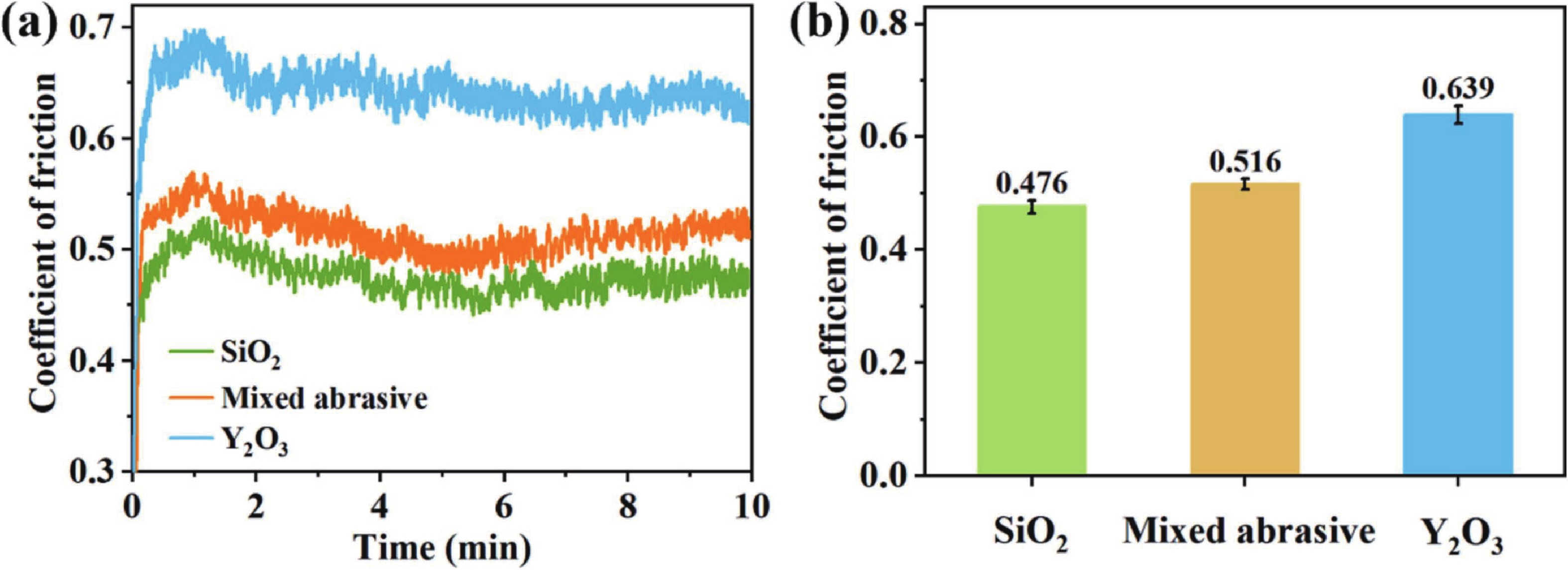
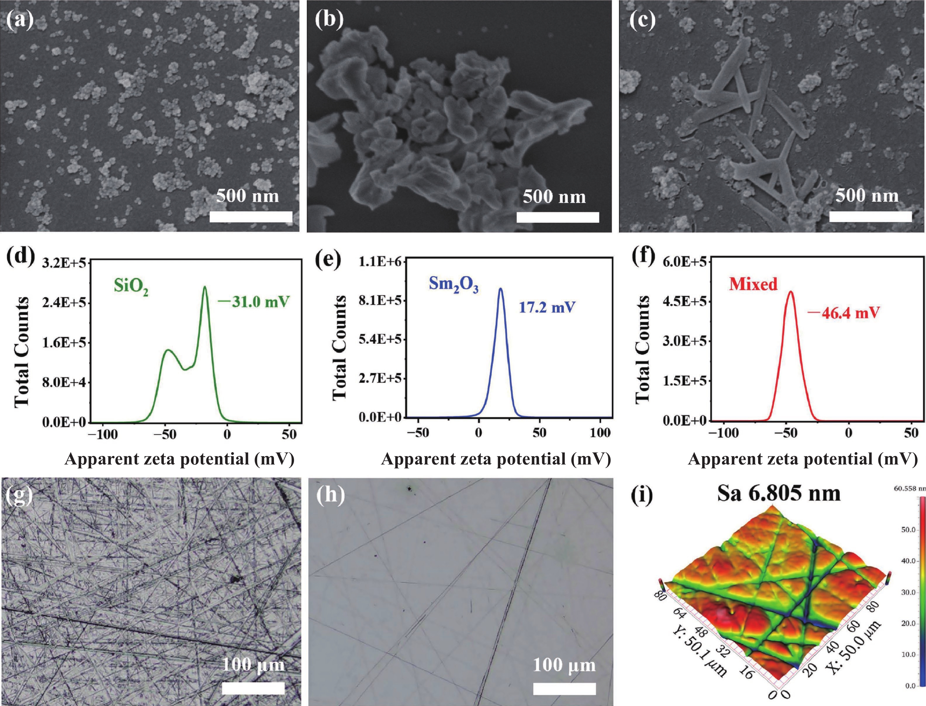
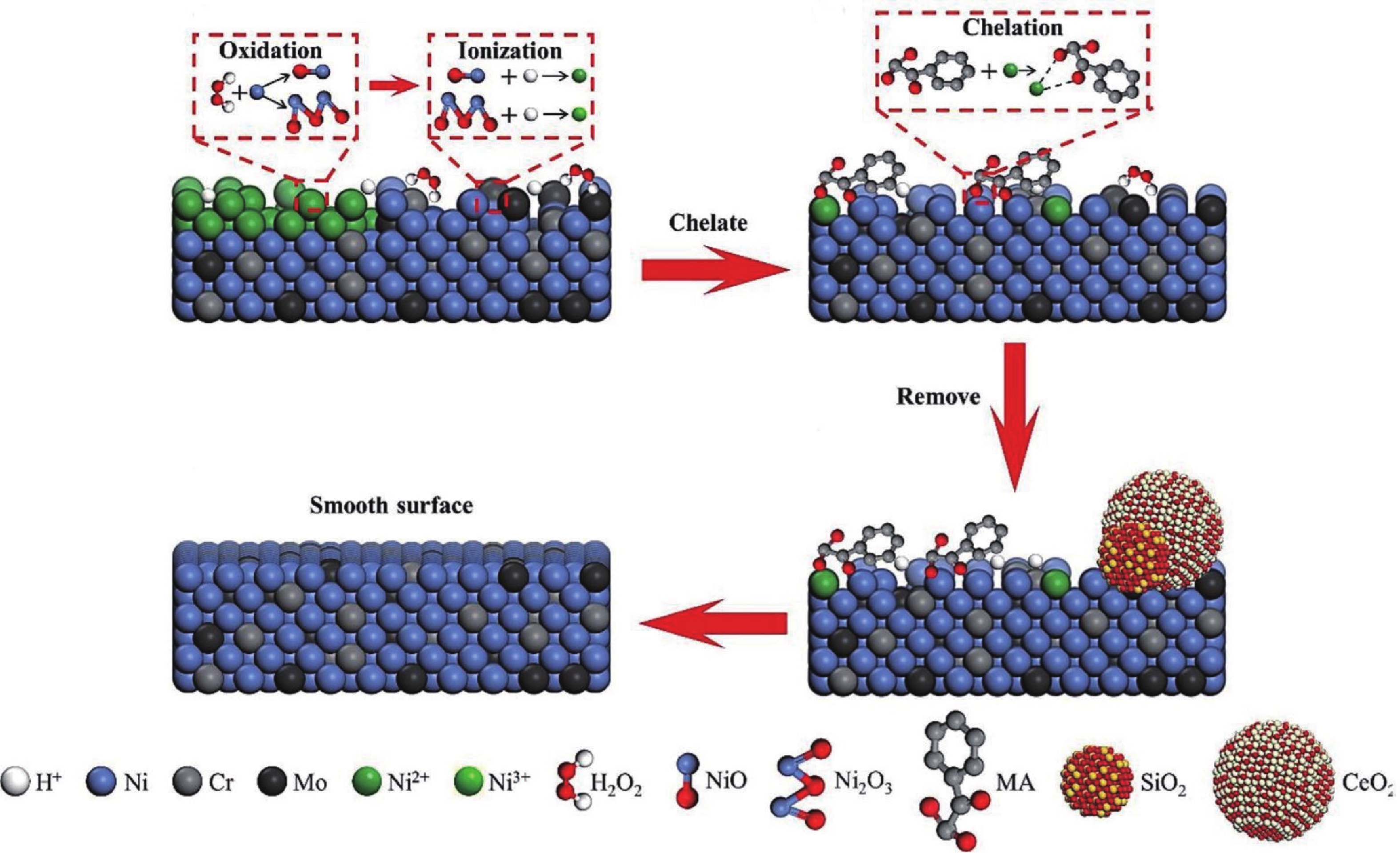
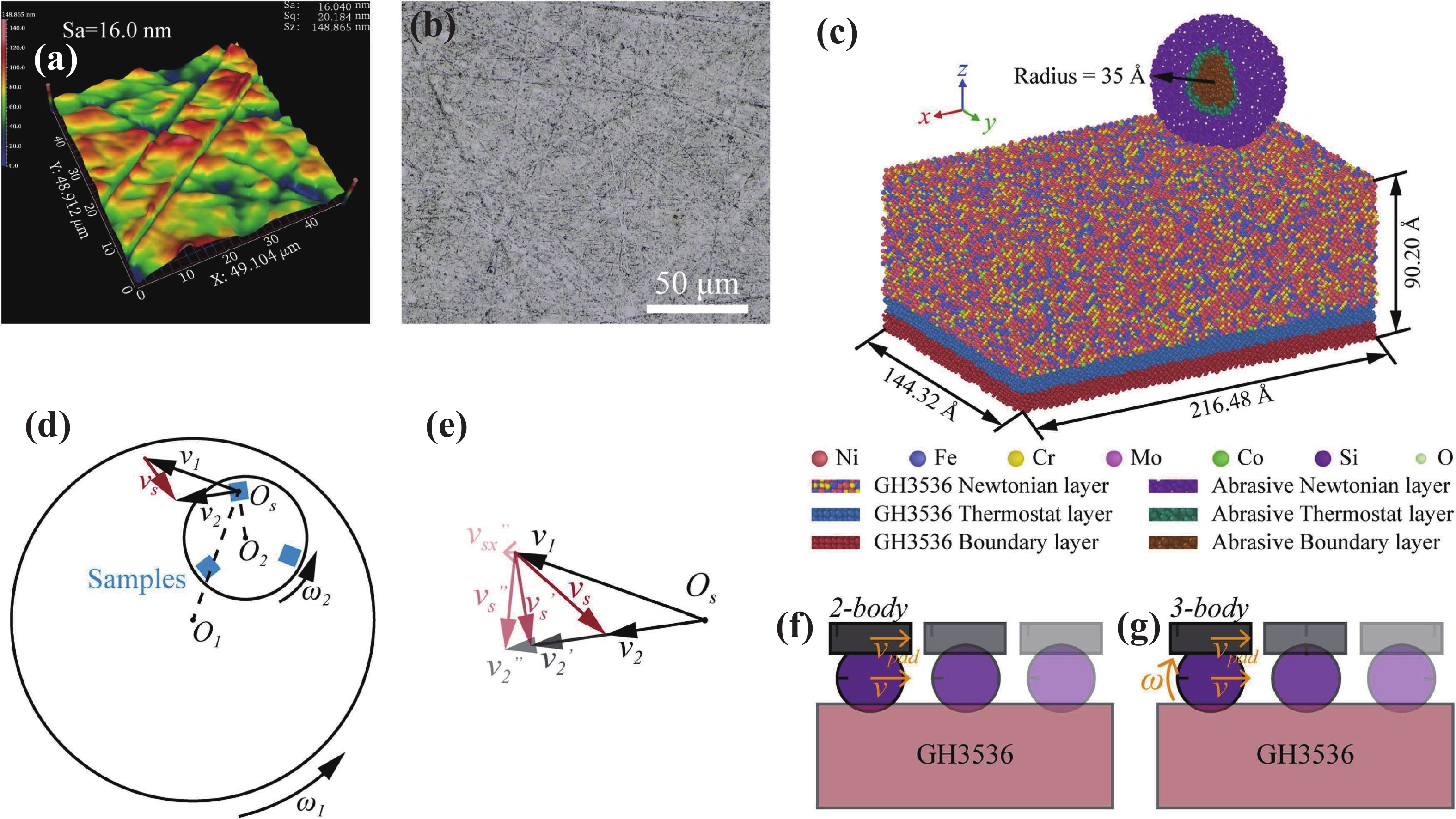
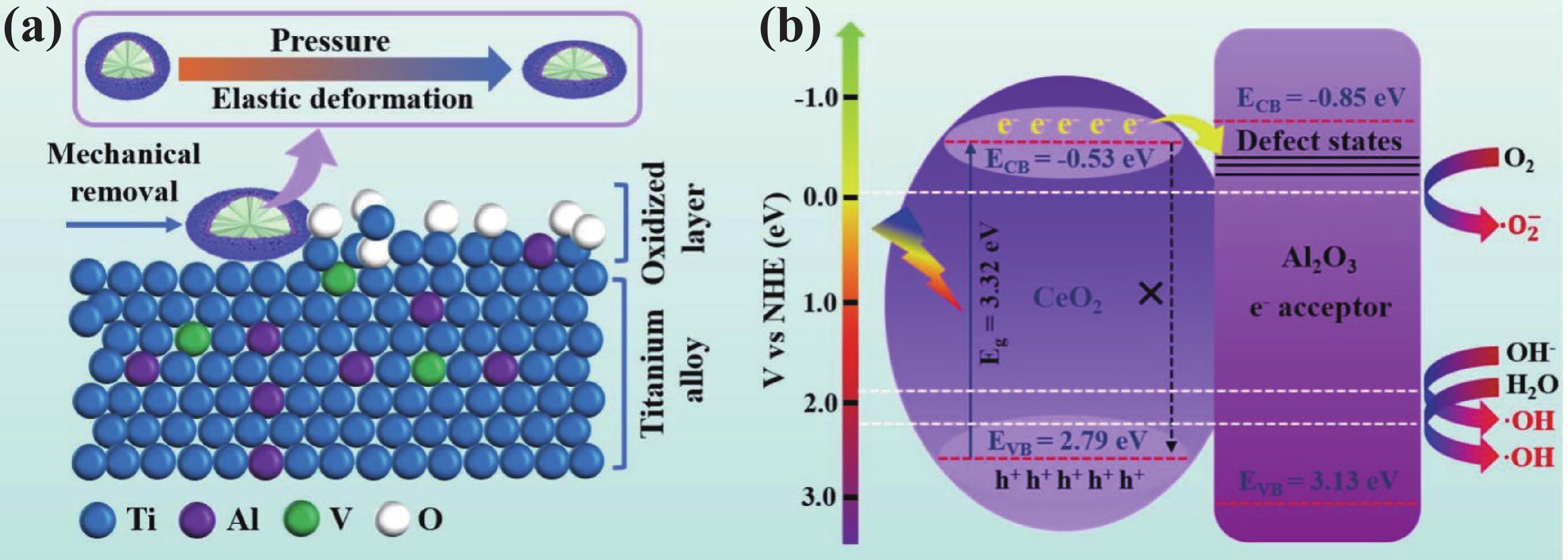
Chemical mechanical polishing (CMP) serves as an indispensable process for achieving global planarization in semiconductor manufacturing, especially as integrated circuit (IC) technology advances to sub-7 nm nodes, where atomic-level surface flatness becomes crucial. Silica abrasives, which account for over 90% of the abrasive market in advanced CMP processes, operate not through simple mechanical grinding but through a key "chemical-mechanical synergistic" mechanism: chemically softening the wafer surface, then mechanically removing the softened layer to expose a new surface, which is further softened and removed, repeating this cycle to produce a smooth wafer. Despite their prevalence, conventional silica abrasives still face challenges, including relatively low material removal rate (MRR), a tendency to agglomerate, leading to poor dispersion and surface defects, and limitations in achieving ultimate surface uniformity. Significant progress has been made to address these issues. Development has progressed from simple spherical particles to complex structural designs (such as mesoporous, hollow, and raspberry-shaped structures) to enhance slurry transport and mechanical action. Surface chemical modifications (e.g., using amino or polymer groups) can improve dispersion stability and reduce scratching. Furthermore, composites with other materials (e.g., ceria, polymers) and precise control of particle size distribution are key to enhancing performance. These innovative approaches have yielded significant performance gains. State-of-the-art slurries have demonstrated the ability to achieve surface roughness below 0.1 nm RMS. The development of silica abrasives is increasingly focused on sustainability and smart manufacturing. A prominent direction is the design of biodegradable abrasives that disintegrate after use, thereby simplifying post-chemical mechanical polishing (CMP) cleanup and minimizing environmental impact—an approach fully aligned with green manufacturing principles. This review systematically summarizes the progress of silica abrasives for CMP over the past 60 years. This summary provides theoretical insights and forward-looking strategies to overcome the current limitations of abrasive technology. We believe this review will be helpful in advancing the field of CMP abrasives towards next-generation semiconductor manufacturing.
J. Semicond.
2026, 47(4): 041801 doi: 10.1088/1674-4926/25120014

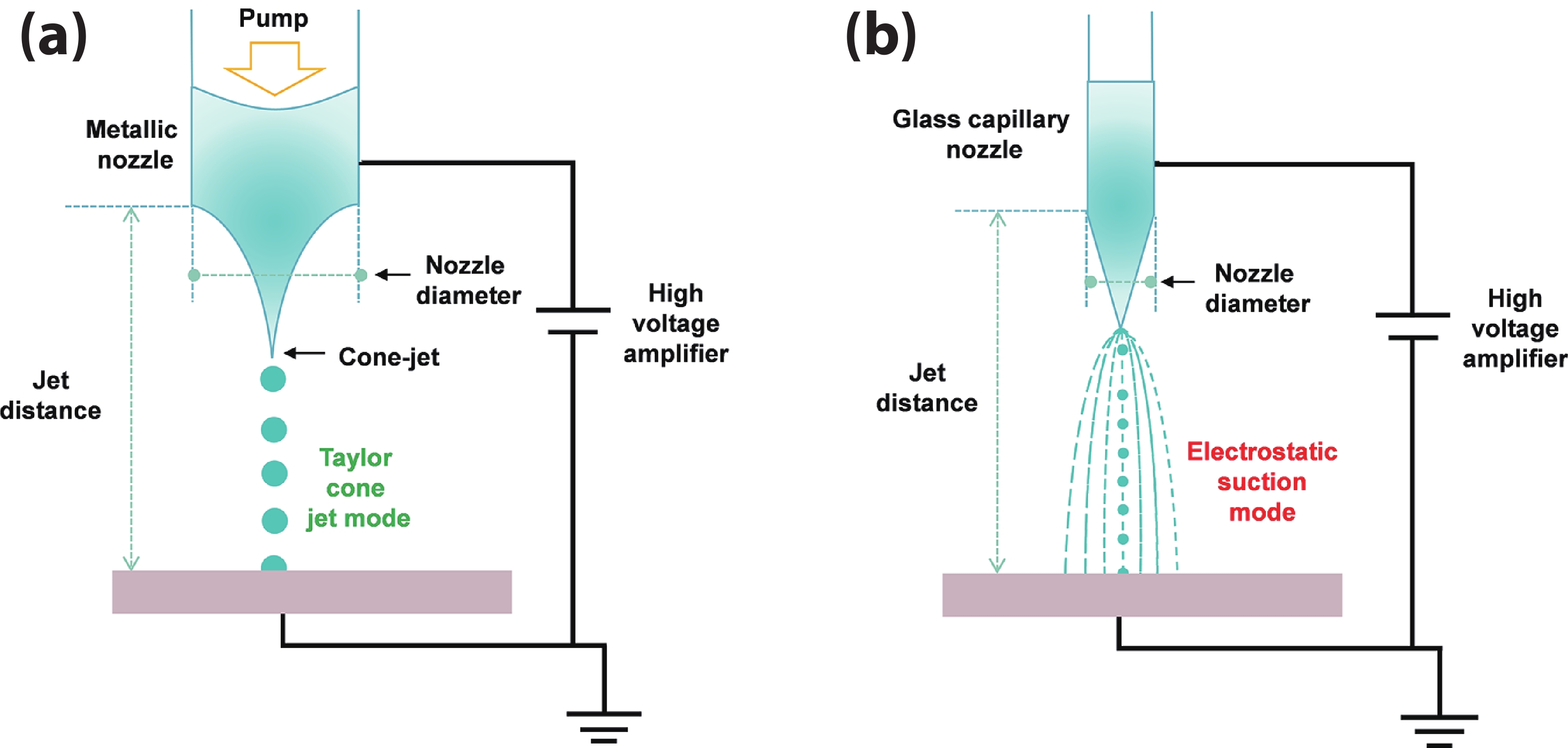
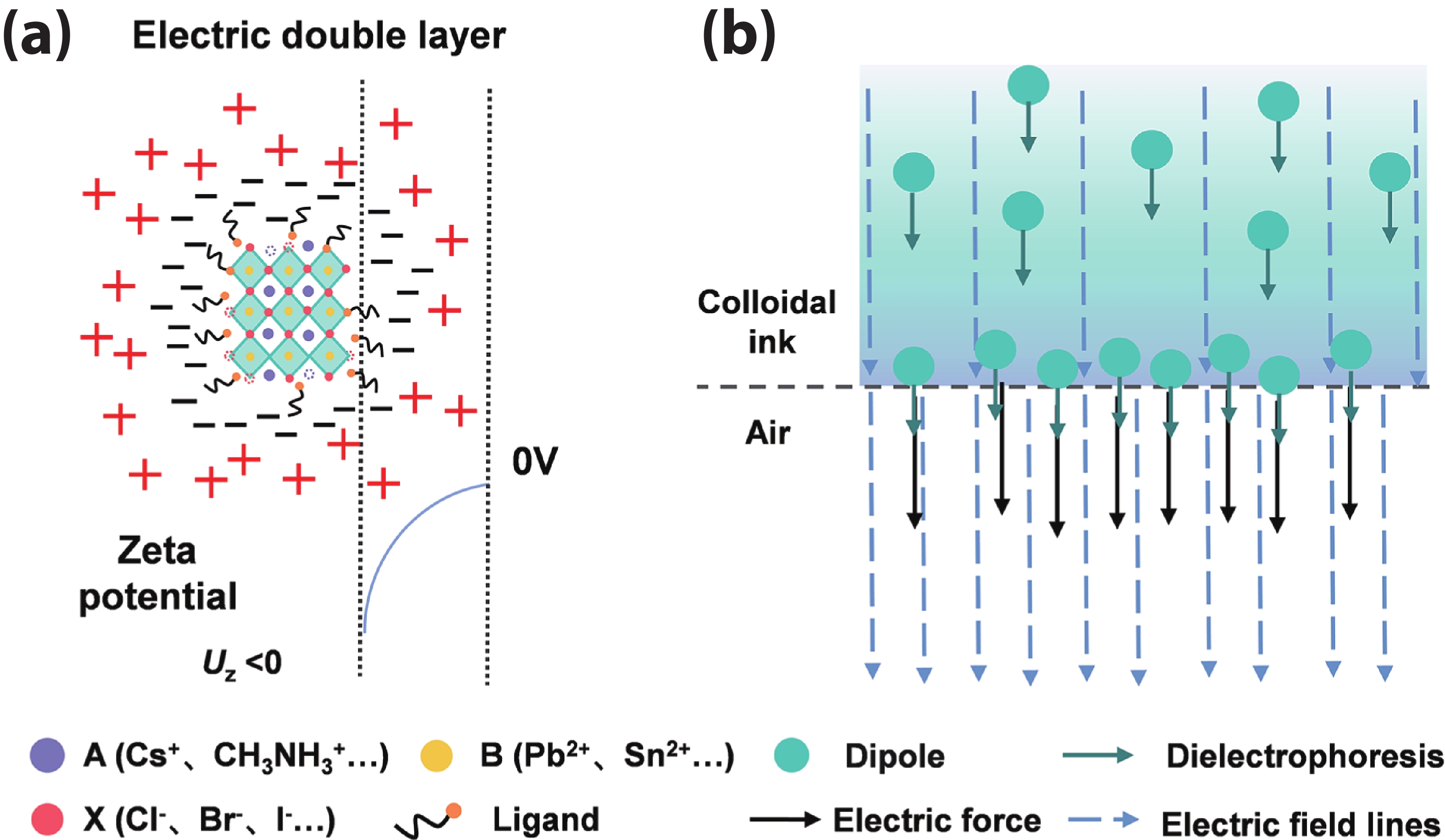
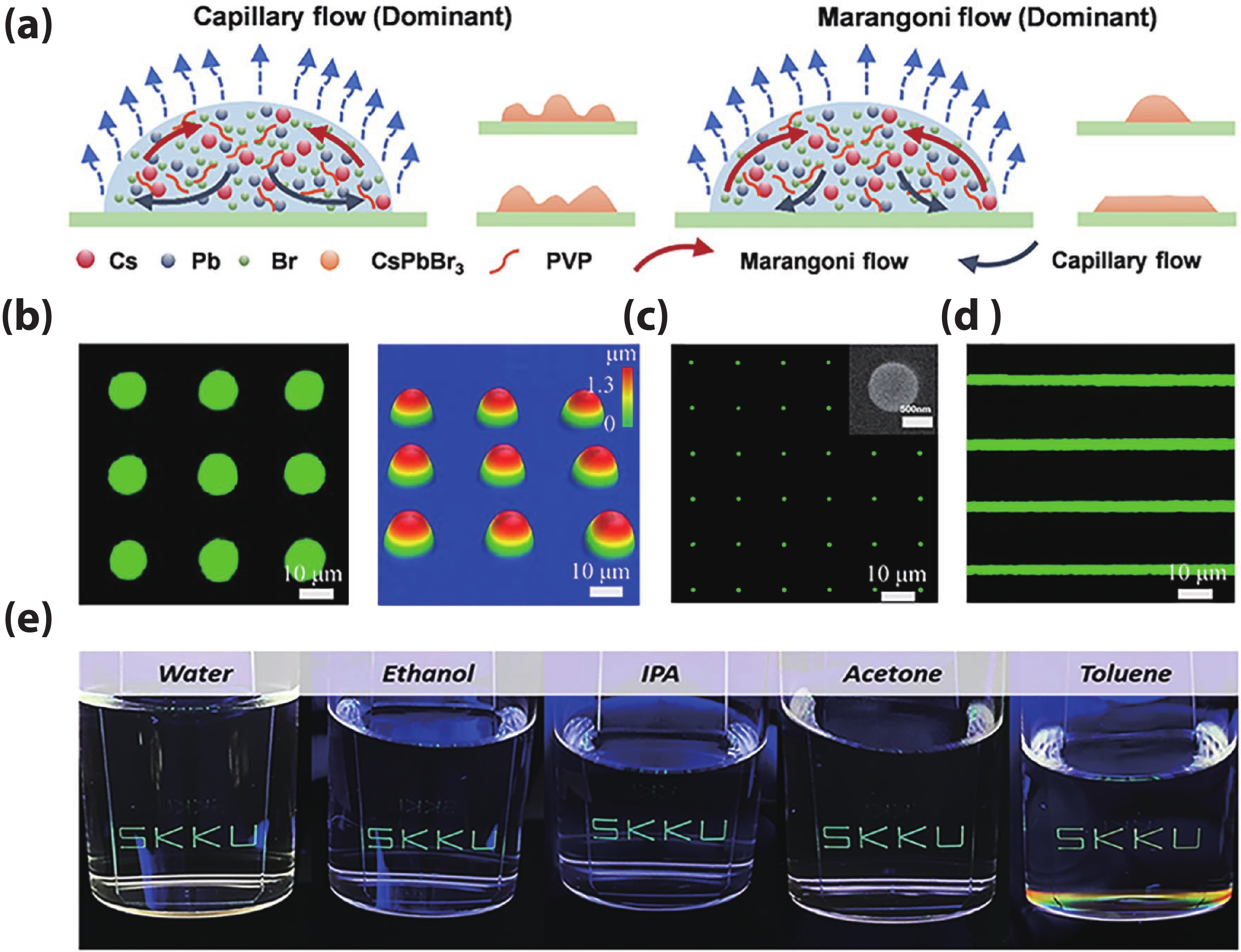
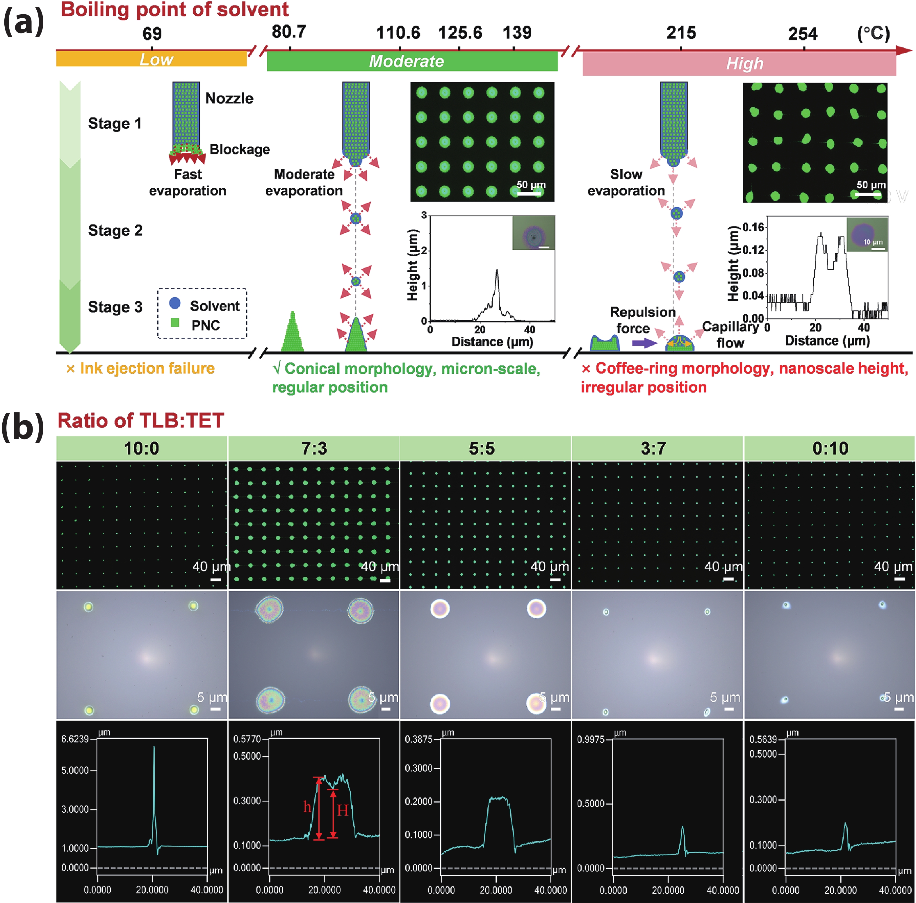
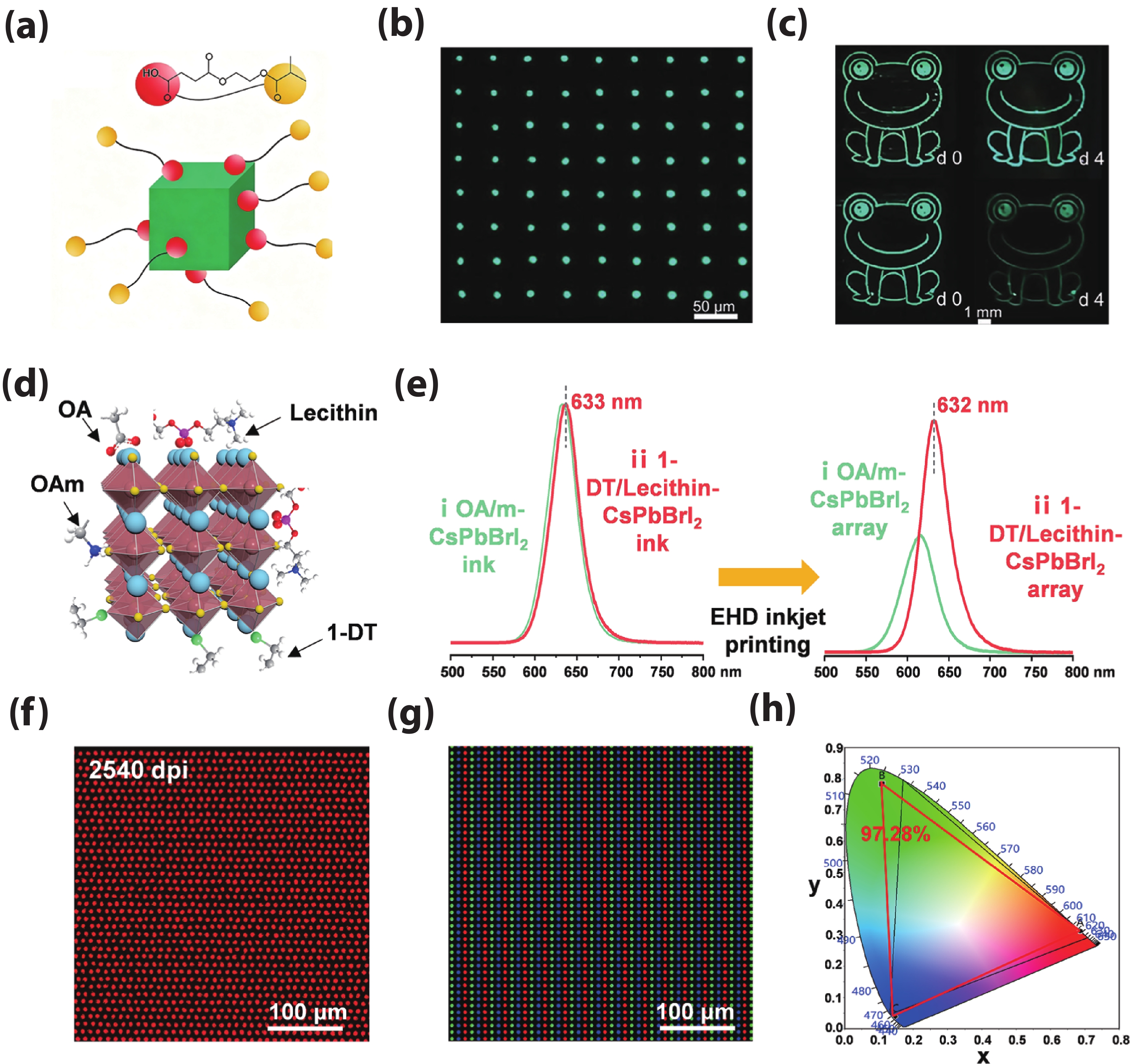
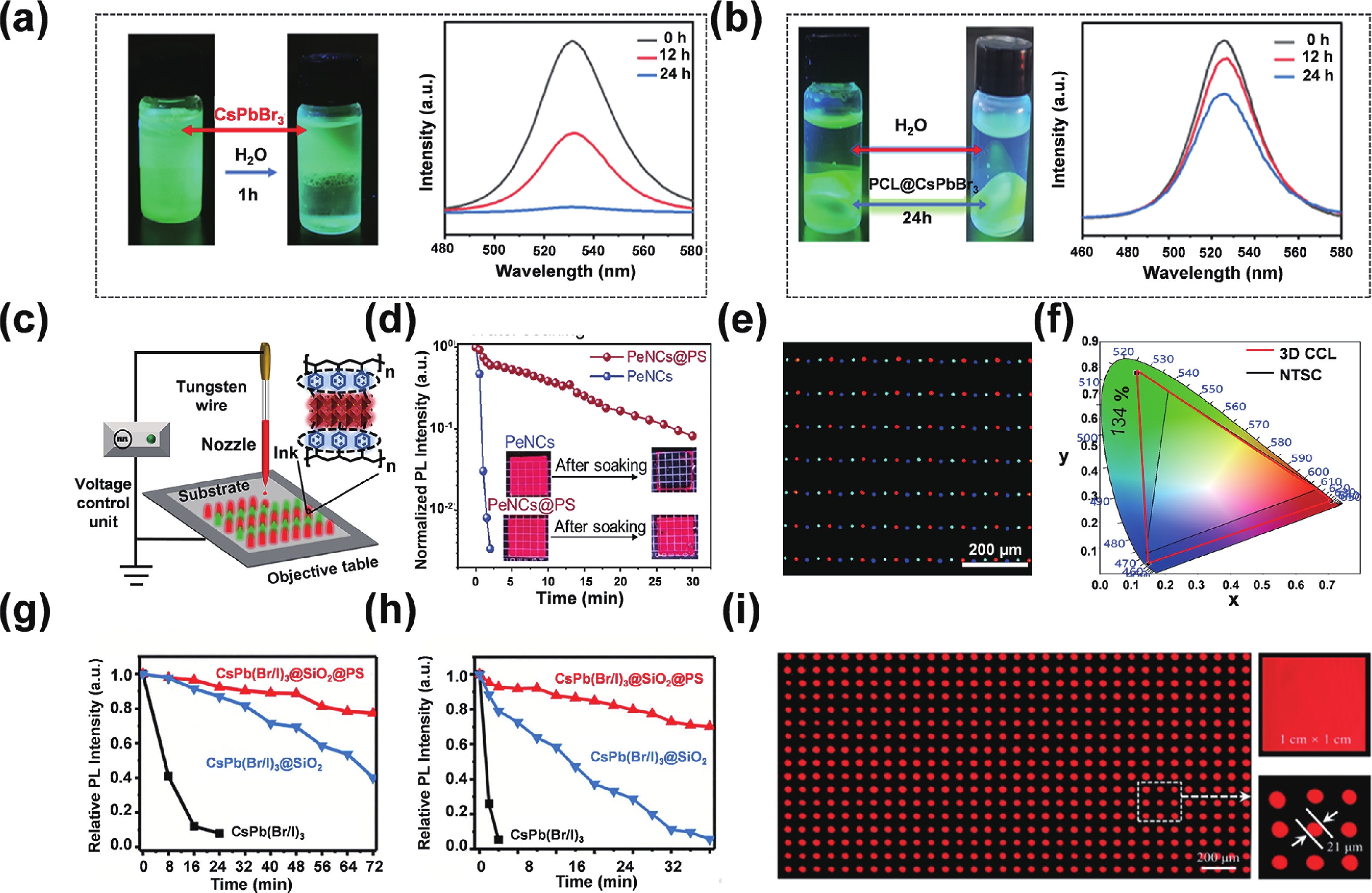
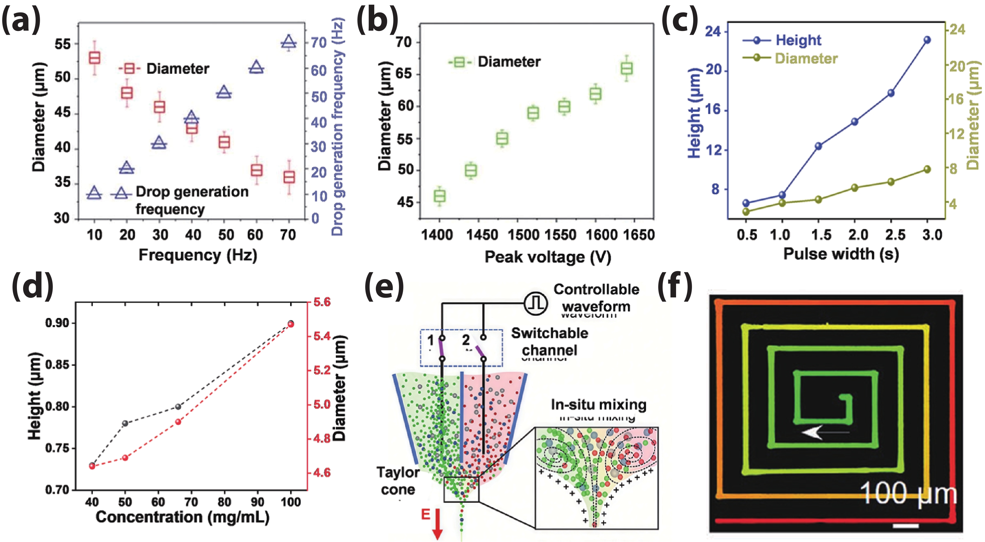
Electrohydrodynamic (EHD) inkjet printing has emerged as a powerful micro-/nanofabrication technique for high-resolution perovskite quantum dot (PeQD) color-conversion layers, offering precise control over pixel morphology, dimensions, and composition. This review systematically examines the mechanisms of cone-jet and electrostatic-attraction modes in EHD printing, highlighting recent advances in PeQD ink design, solvent and ligand engineering, and printing parameter optimization. Perovskite precursor and colloidal inks are discussed in detail, emphasizing strategies to enhance droplet ejection stability, suppress coffee-ring effects, and achieve uniform, high-luminescence pixels. Ligand exchange, dual-ligand passivation, and core−shell or polymer encapsulation are shown to effectively mitigate ion migration, surface defects, and environmental degradation, thereby improving photoluminescence efficiency and stability. Multi-channel and multi-nozzle EHD printing systems enable dynamic halide composition control and parallel RGB pixel deposition, facilitating ultrahigh-resolution patterning down to submicron feature sizes. Finally, the review highlights future directions, including synergistic PeQD material synthesis, advanced ink formulation, scalable high-throughput printing, and integration of PeQD color-conversion pixels into full-color micro-LED displays with minimal crosstalk and robust operational stability. These developments collectively demonstrate the immense potential of EHD inkjet printing for next-generation high-performance display technologies.
J. Semicond.
2026, 47(4): 042101 doi: 10.1088/1674-4926/25090006
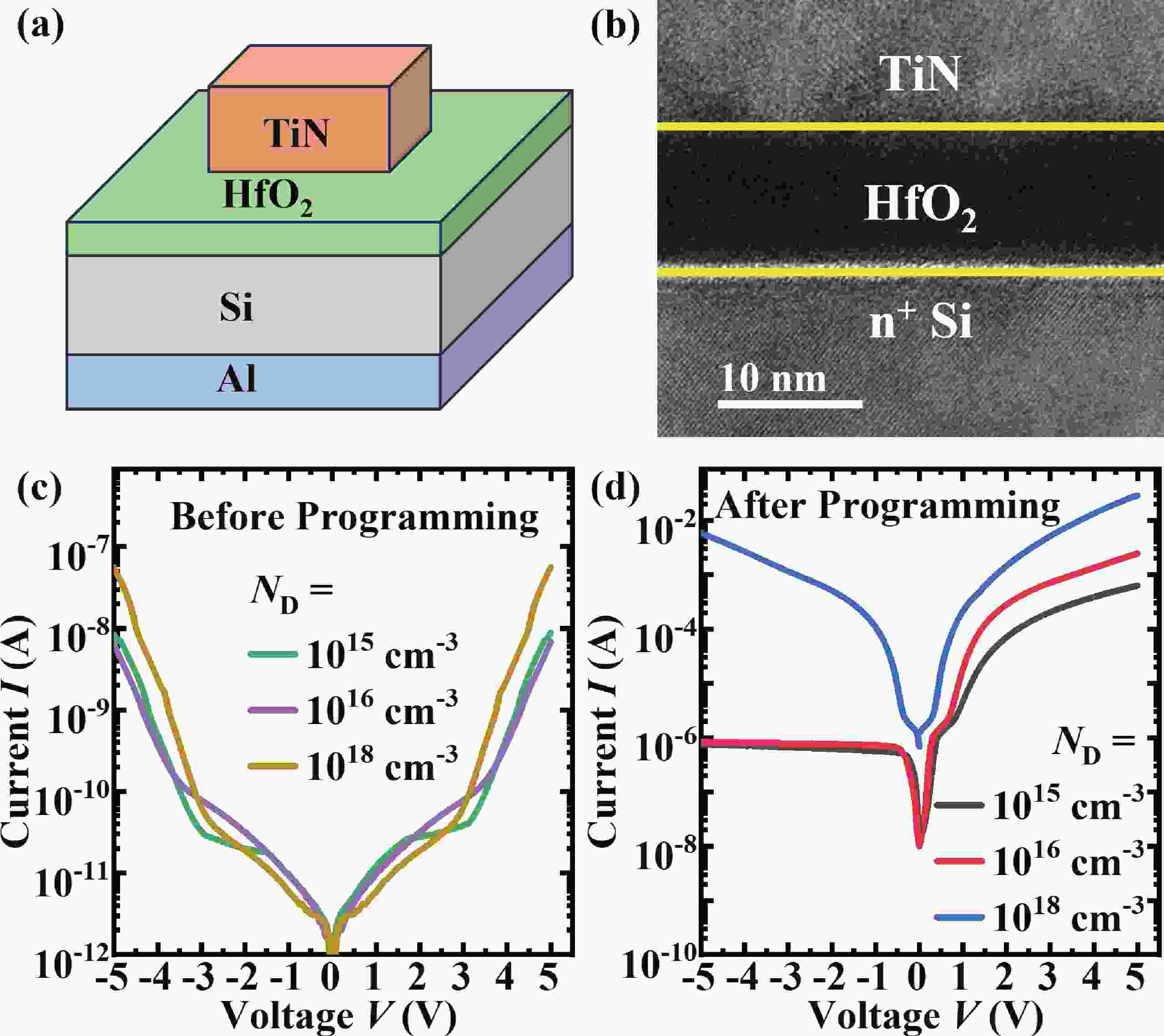
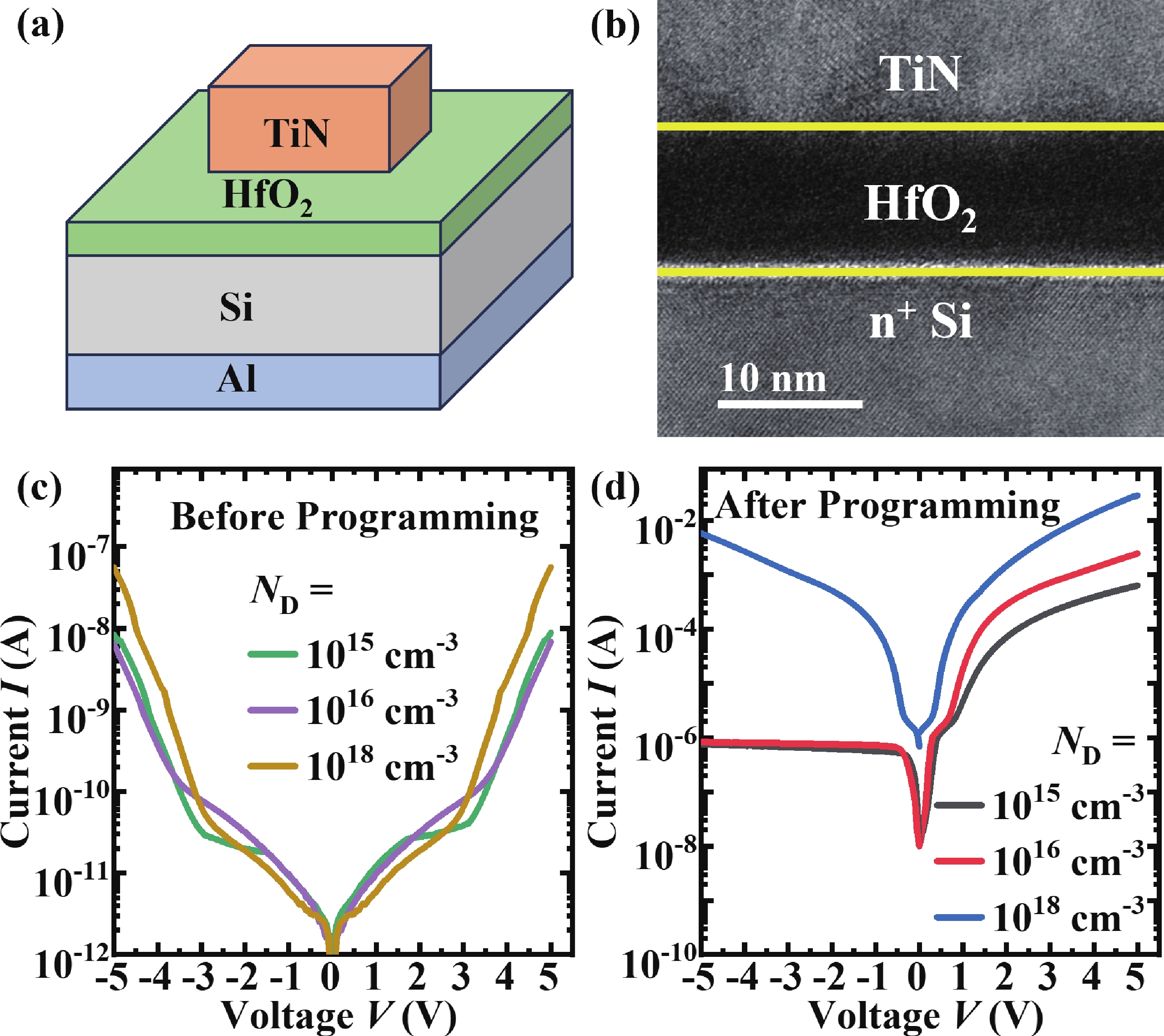
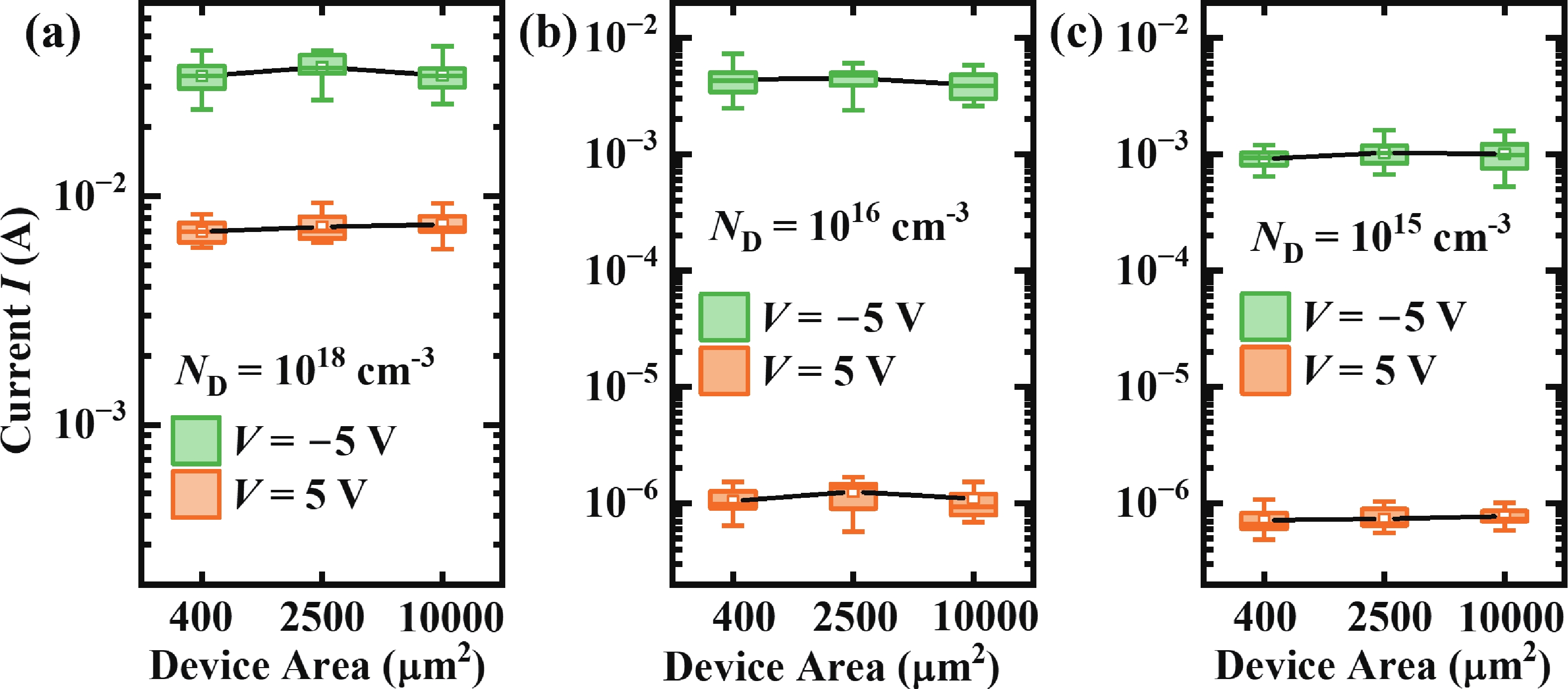
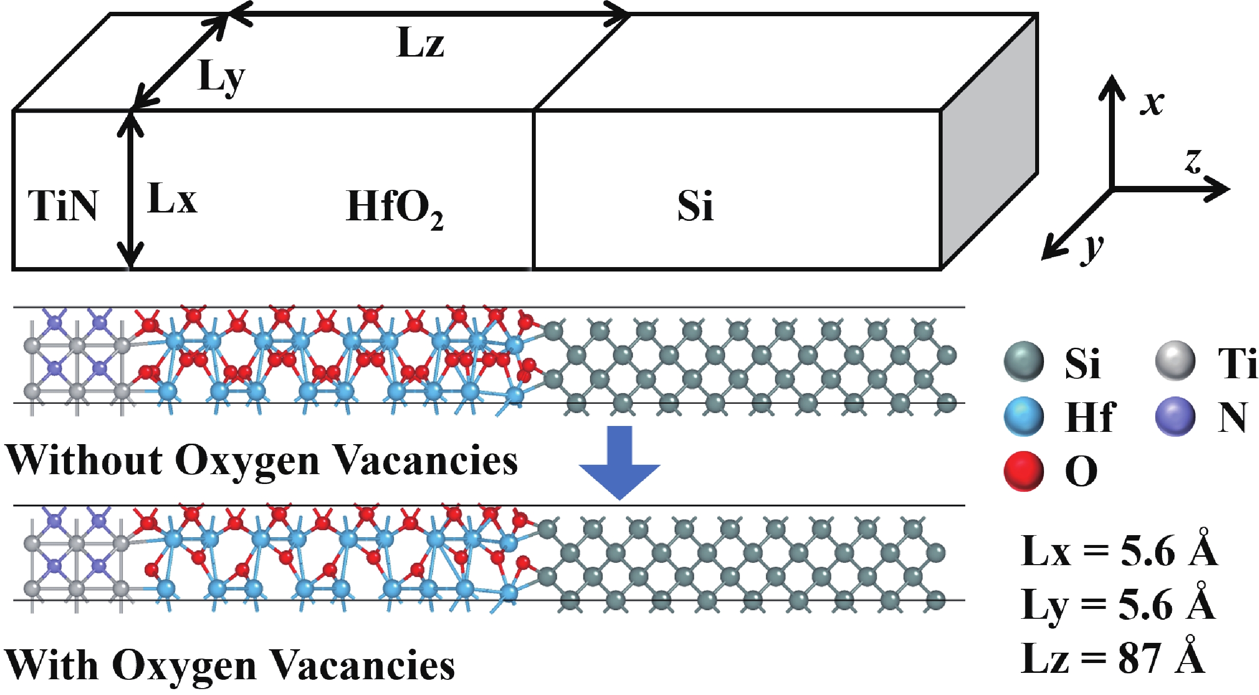
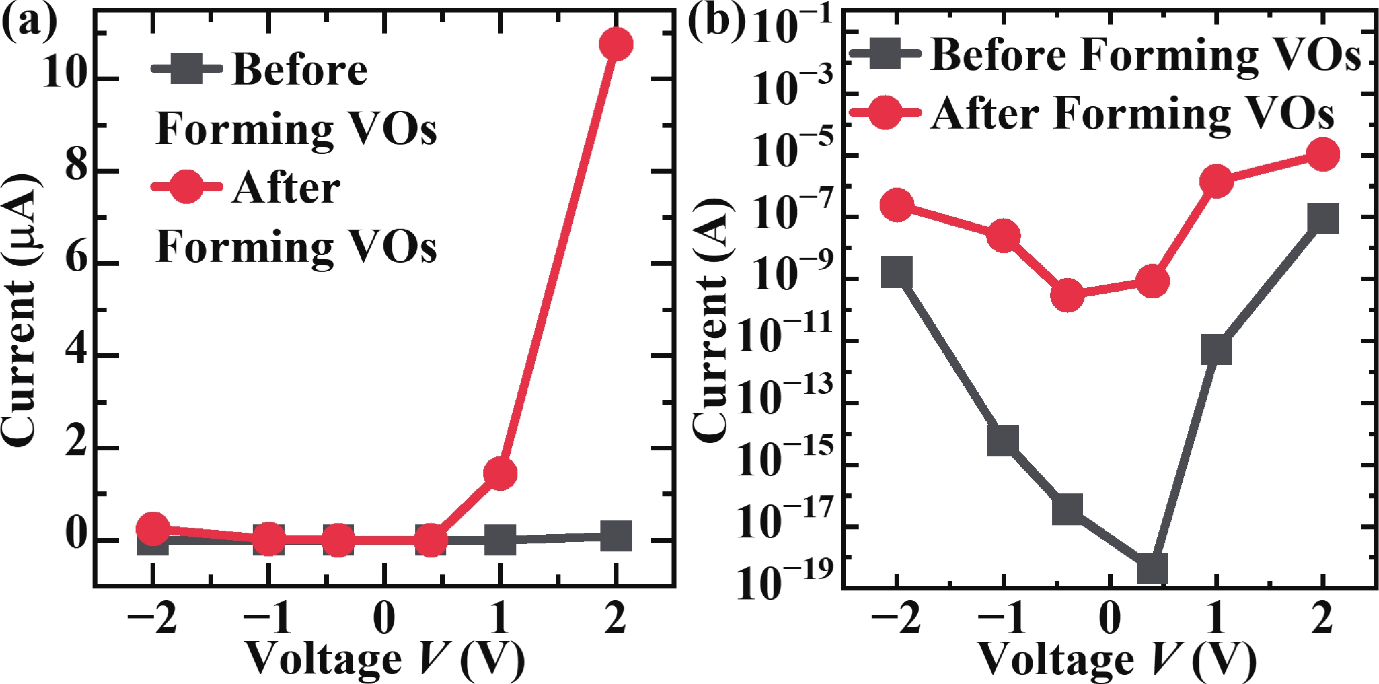
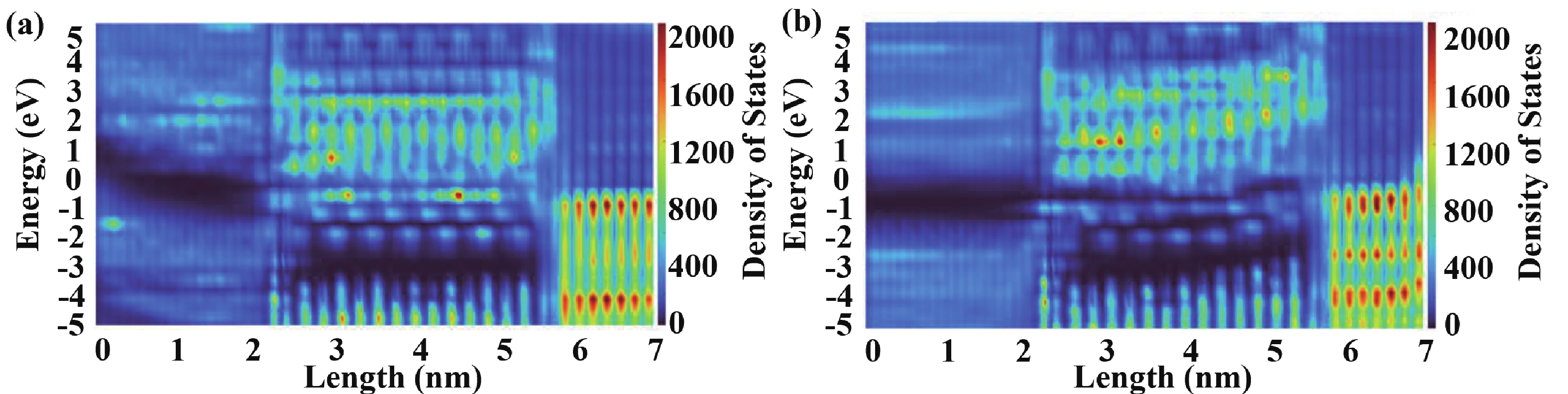
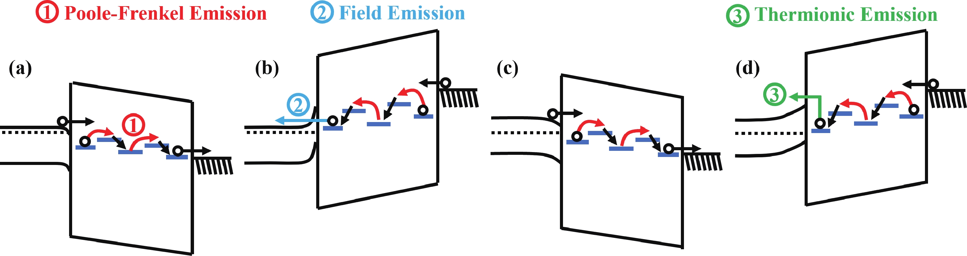
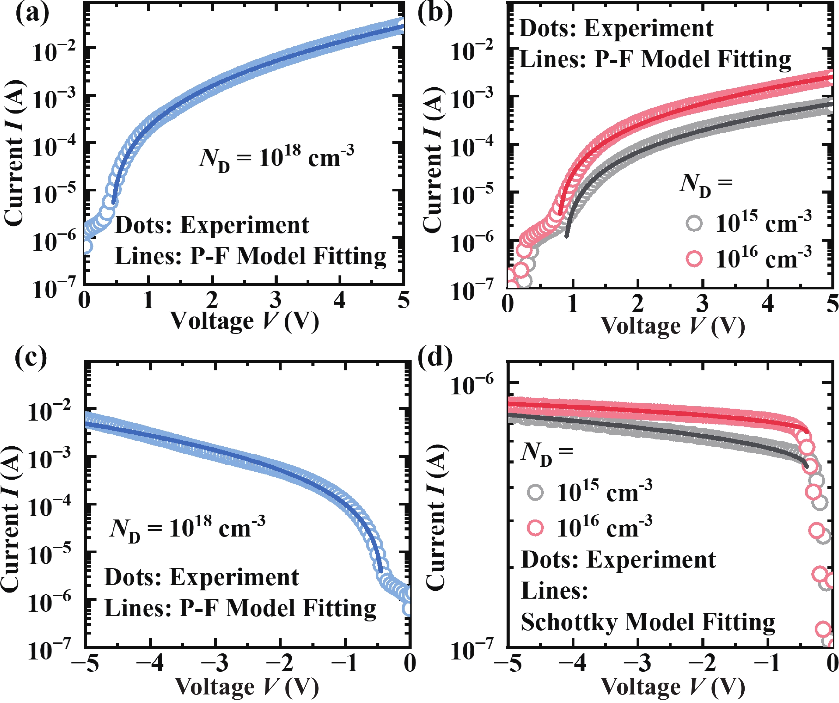
In this work, the oxide-based programmable diodes (PDs) with structure of TiN/HfO2/Si/Al are fabricated, and its electron transport mechanisms are investigated. Electrical measurements results depicted that the conduction and rectification performance of oxide-based PDs are mainly controlled by the interface between oxygen vacancies (VOs) consisted filament and semiconductor electrode. The local density of state in filament and band-bending of the PDs are calculated by first-principal simulation. The electron transport in oxide PDs is dominated by Poole−Frenkel emission under forward bias, while under negative bias, the PDs behave like a reverse Schottky-diode. These mechanisms research is necessary for device optimization and circuit design of oxide-based PDs.
J. Semicond.
2026, 47(4): 042102 doi: 10.1088/1674-4926/25060030
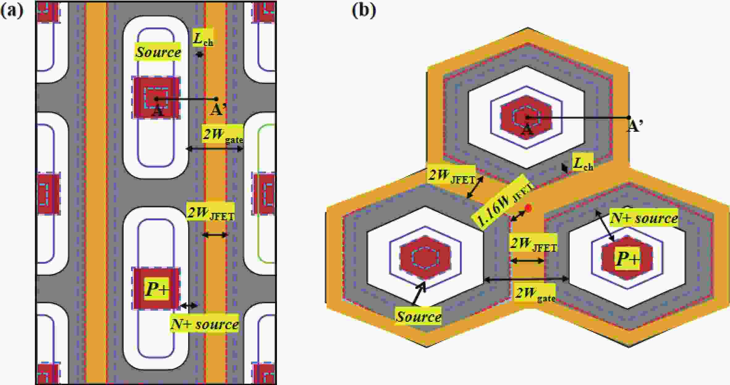
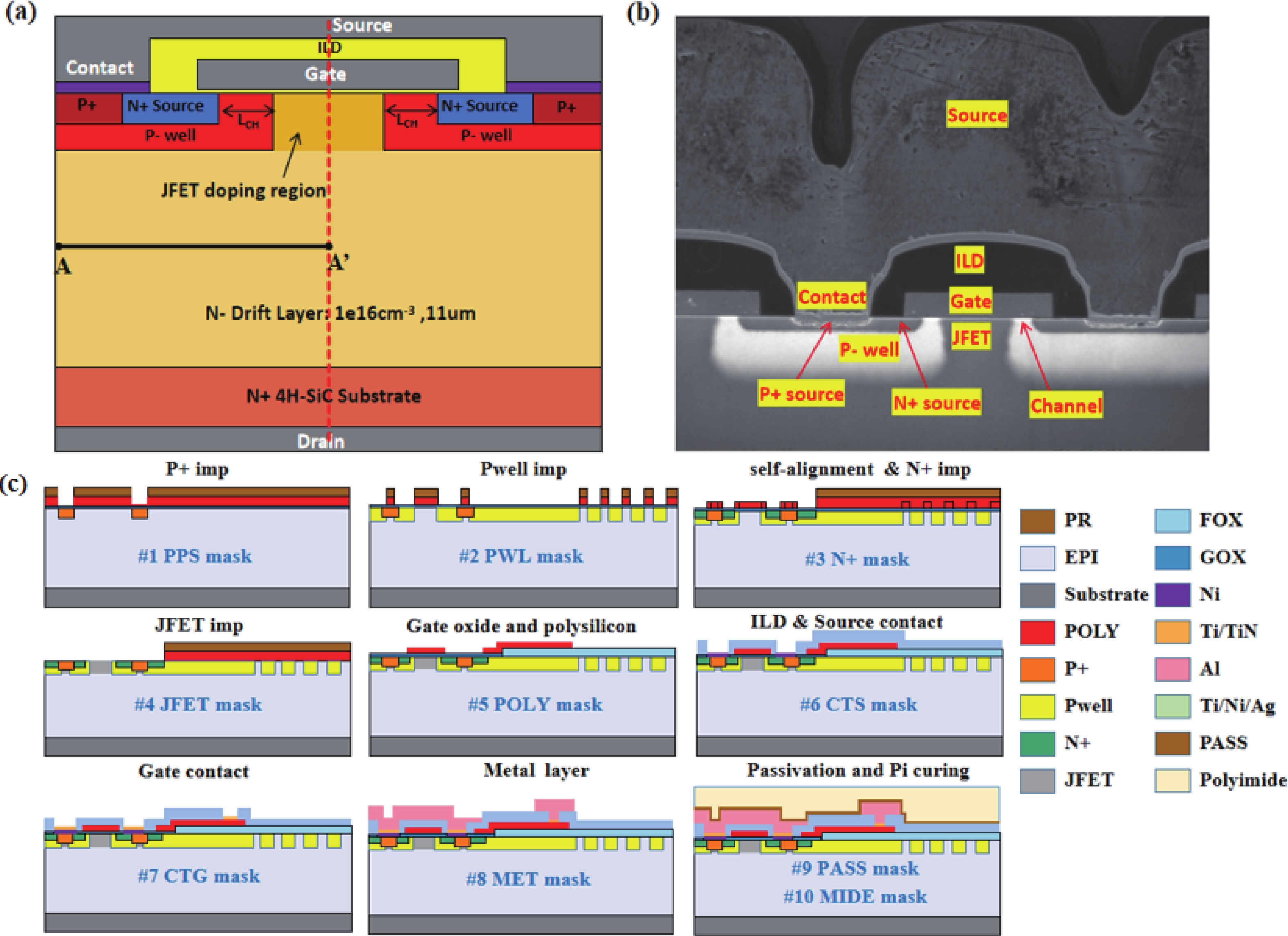
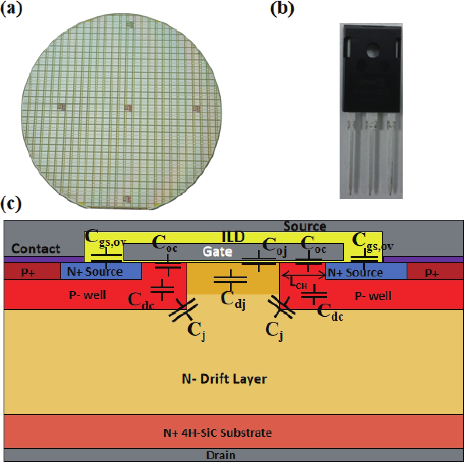
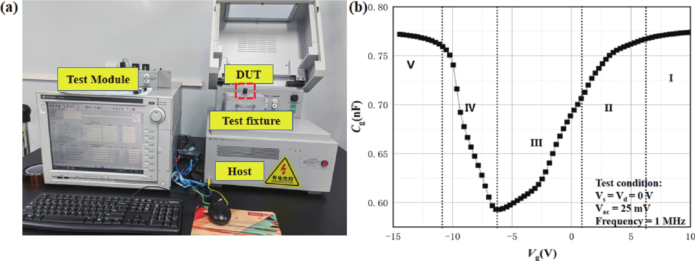
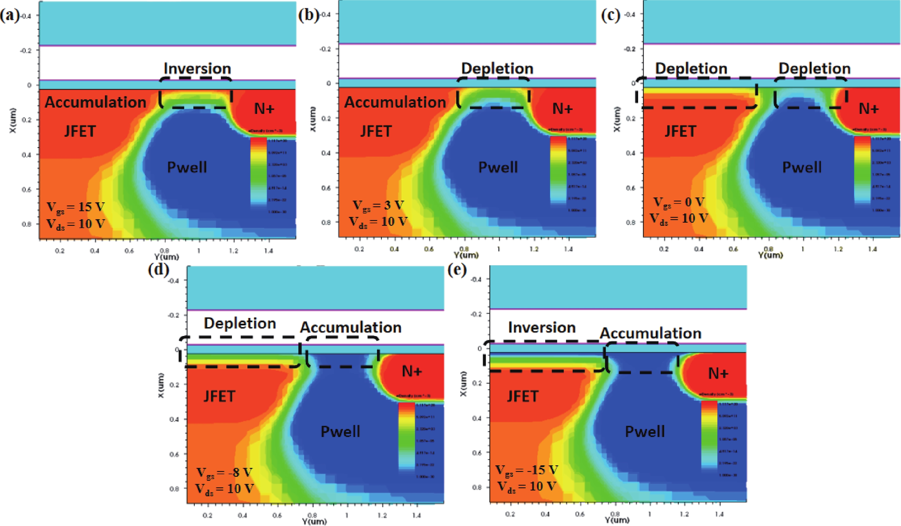
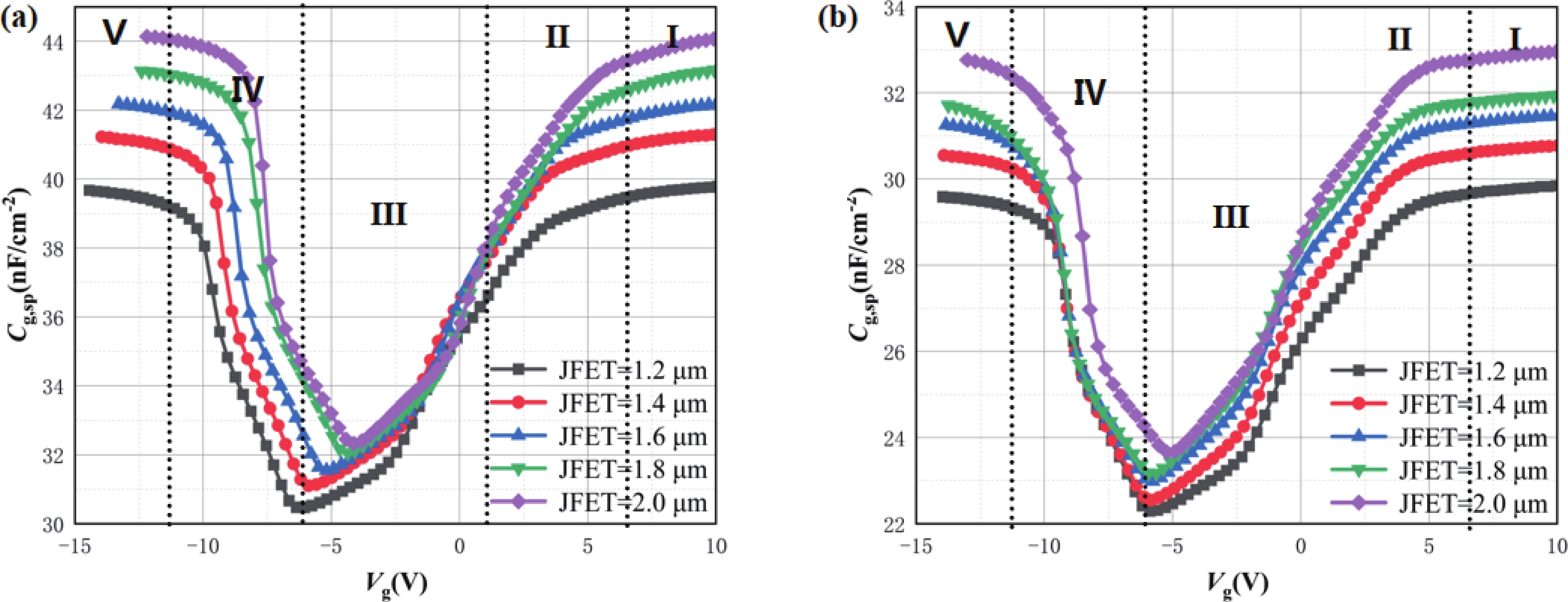
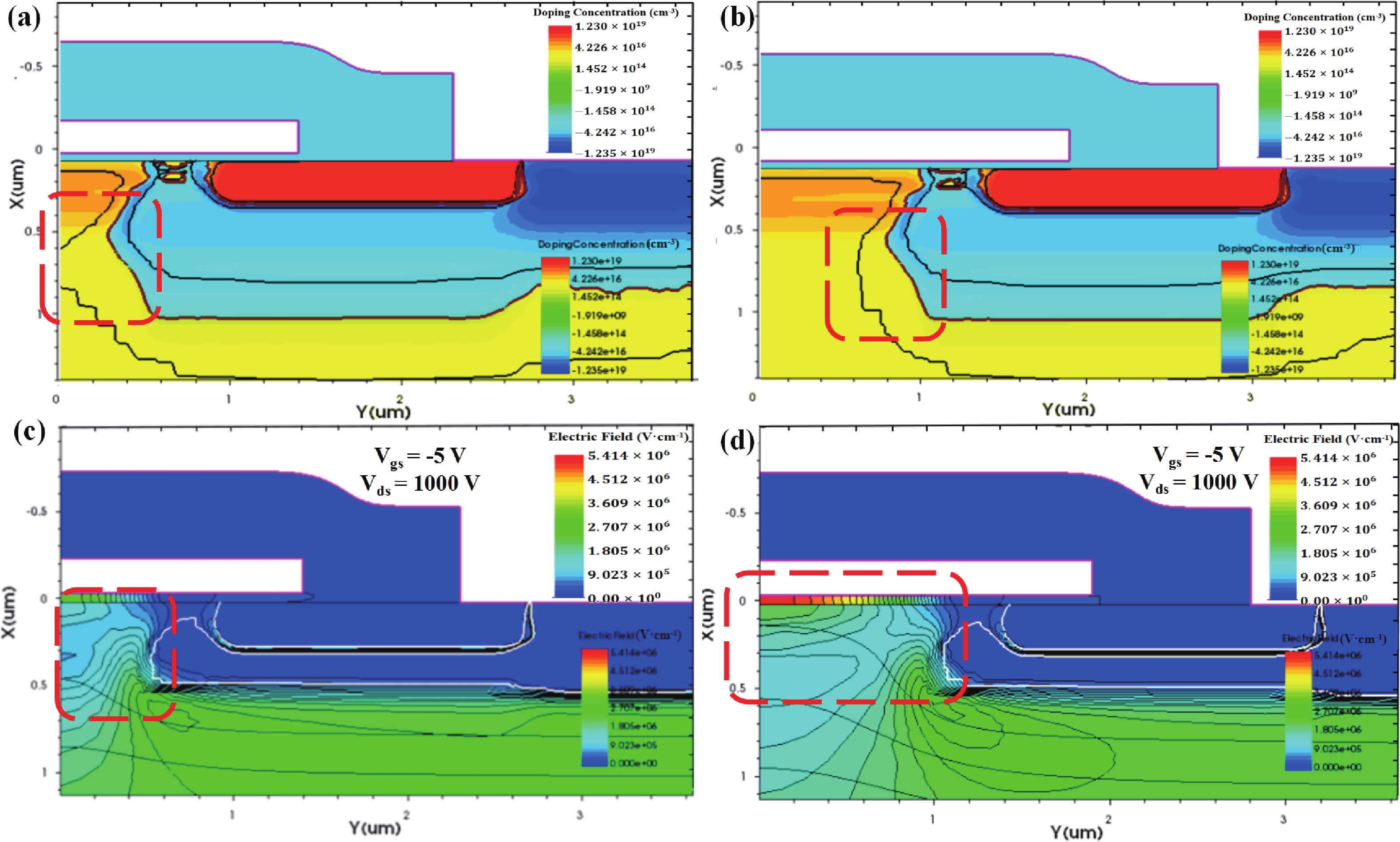
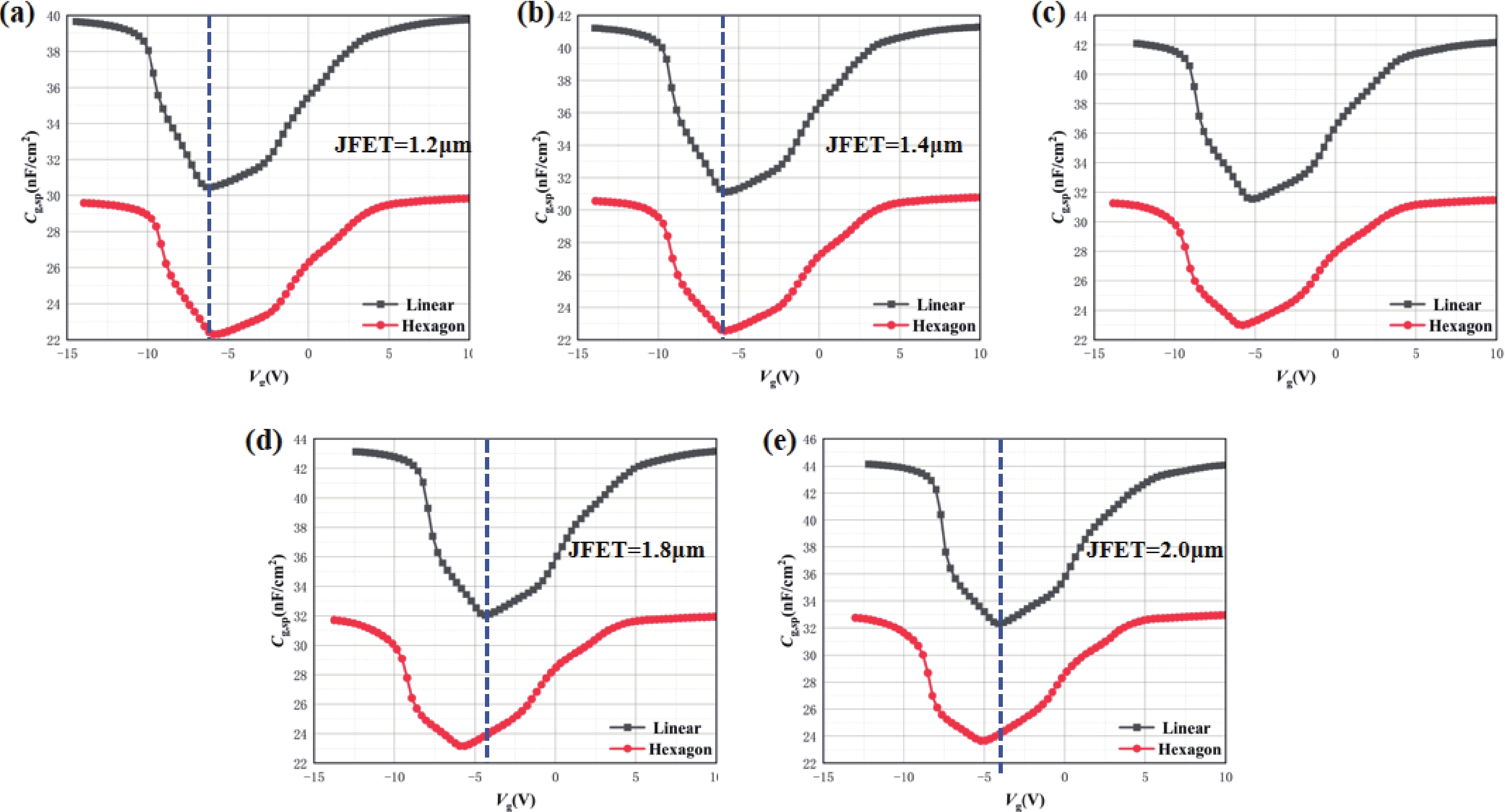
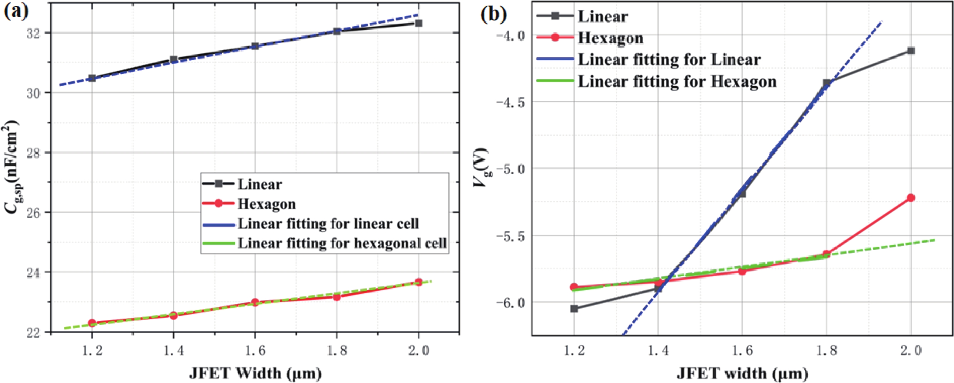
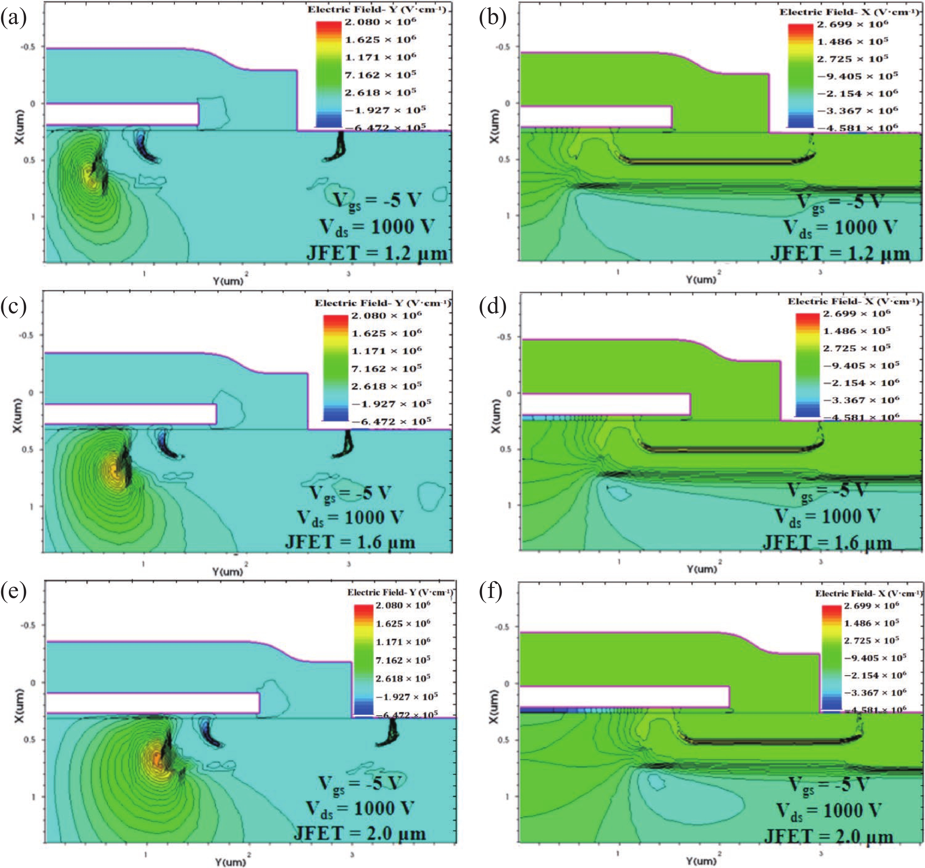
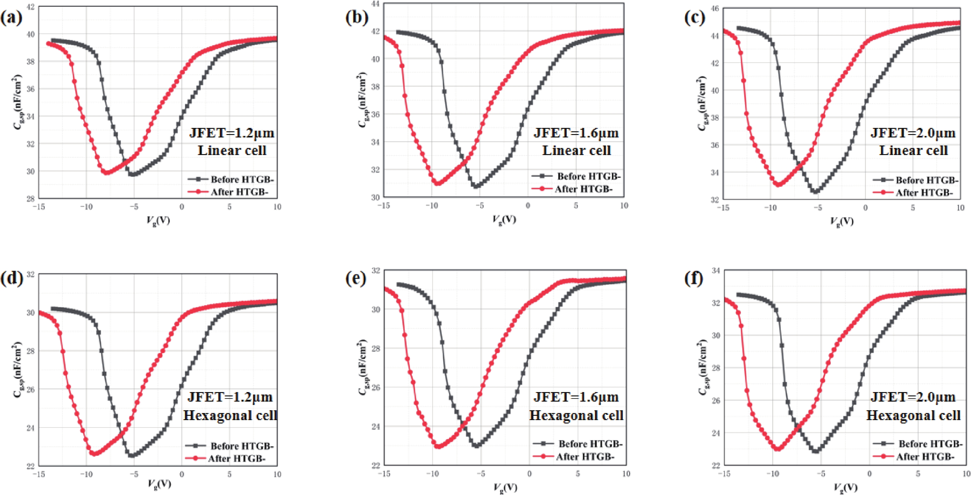
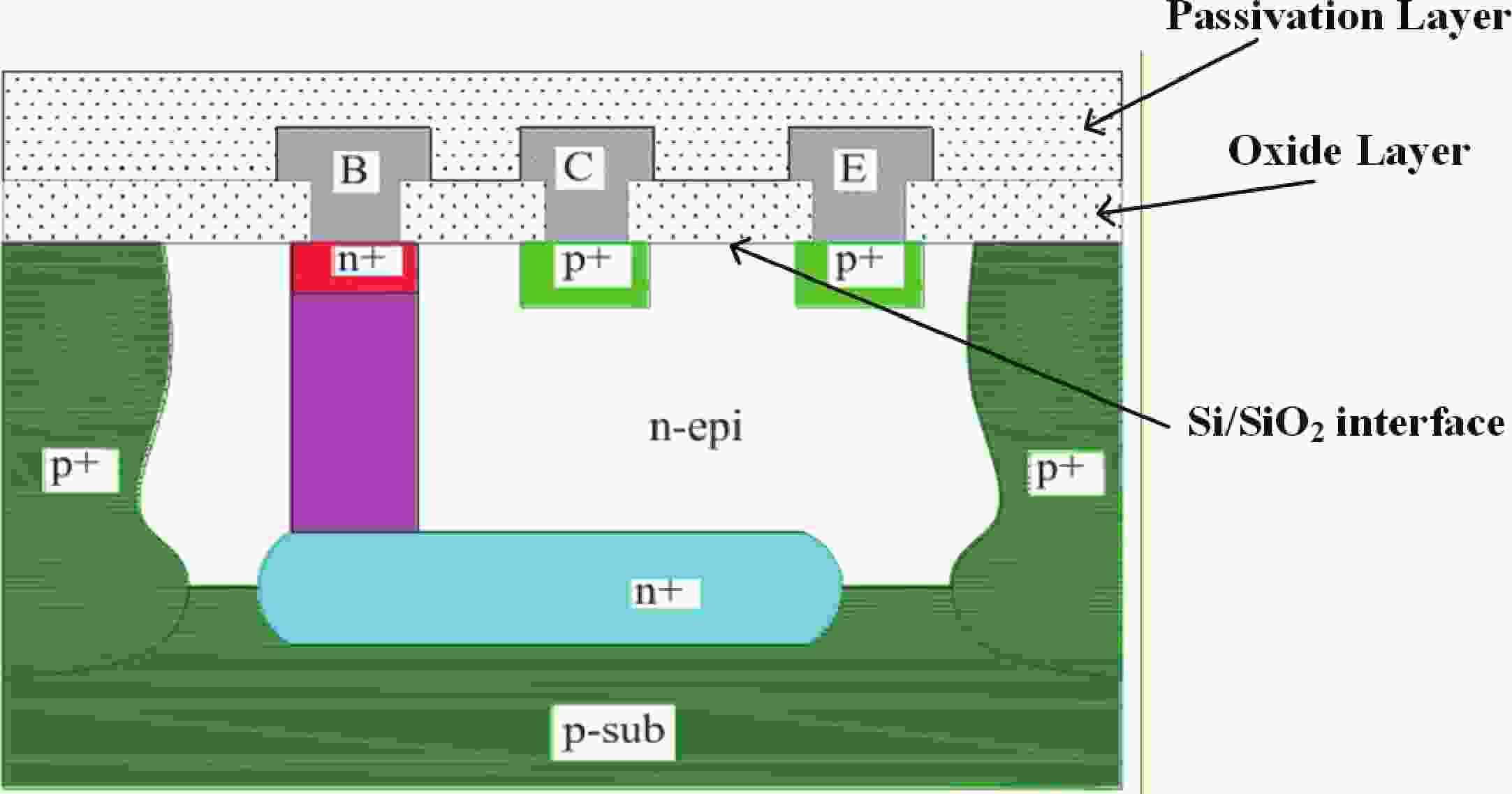
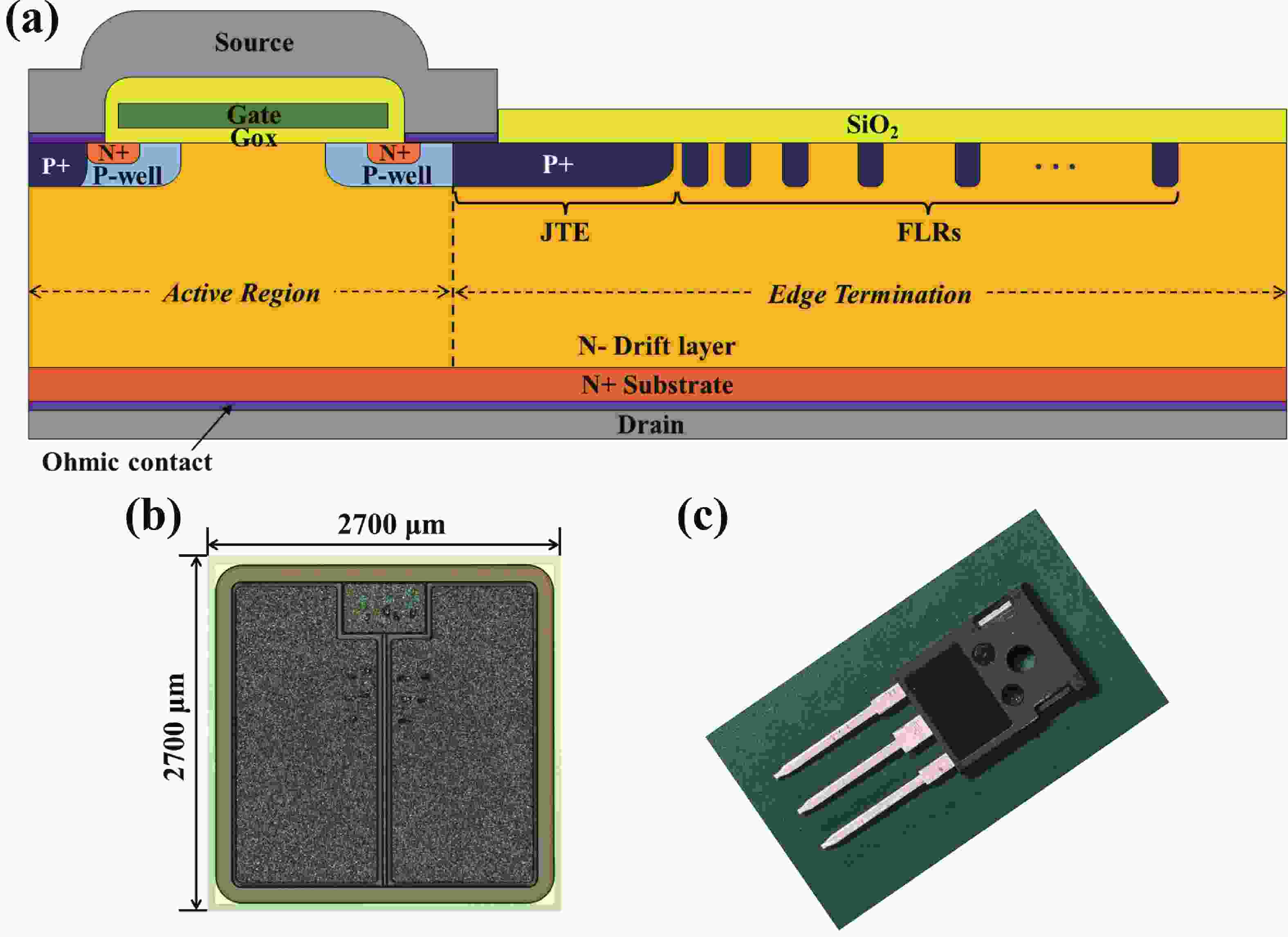
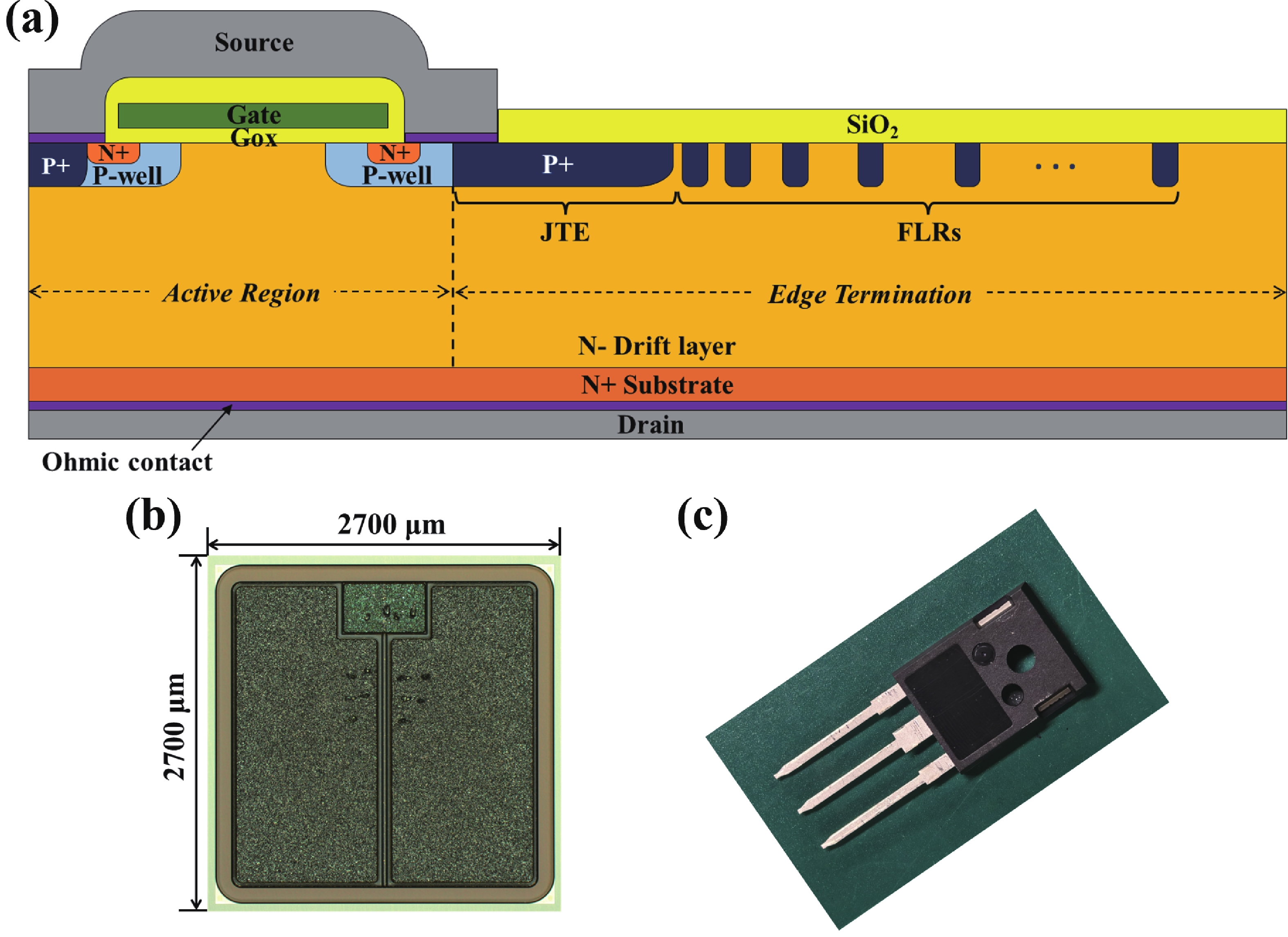
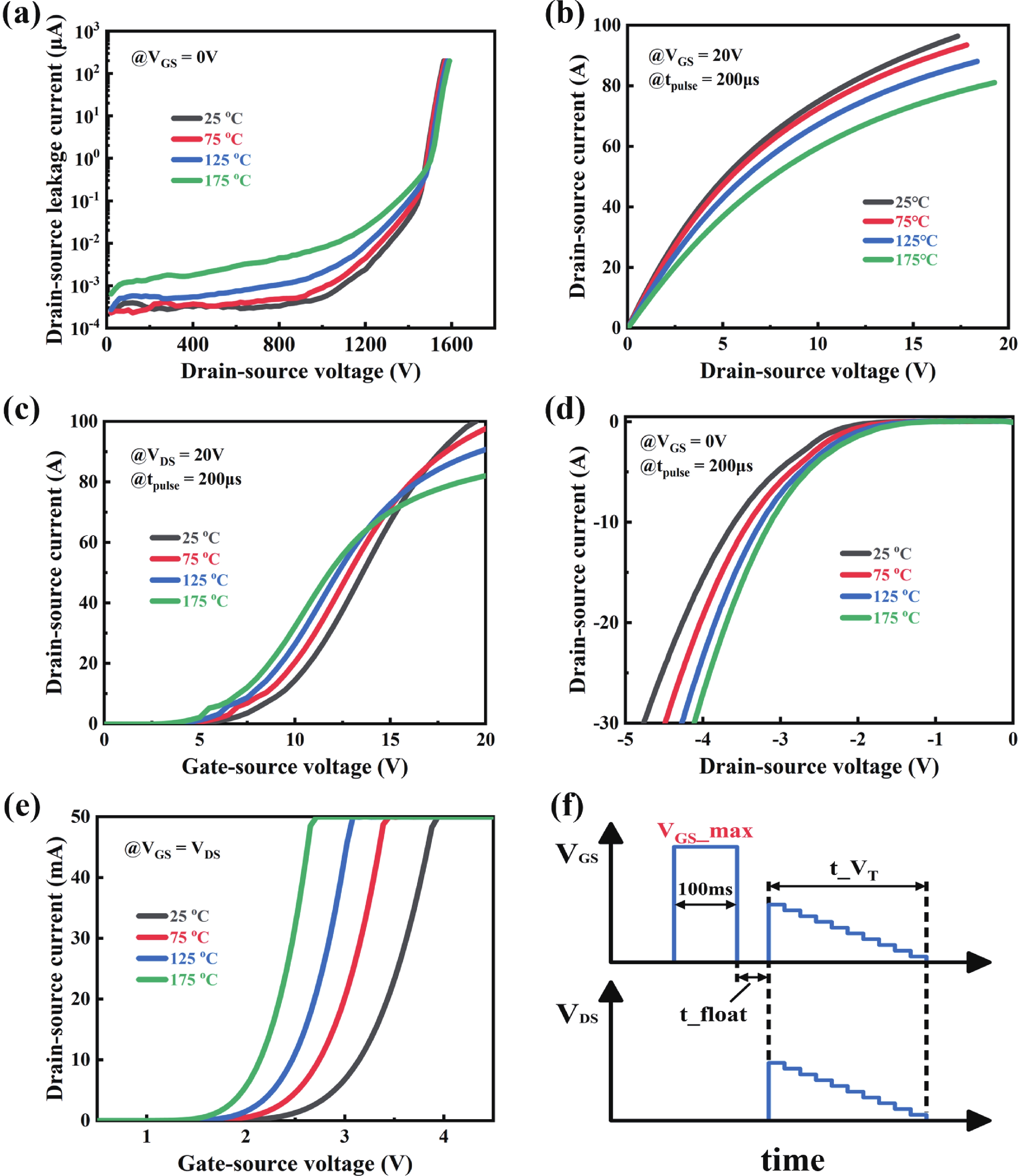
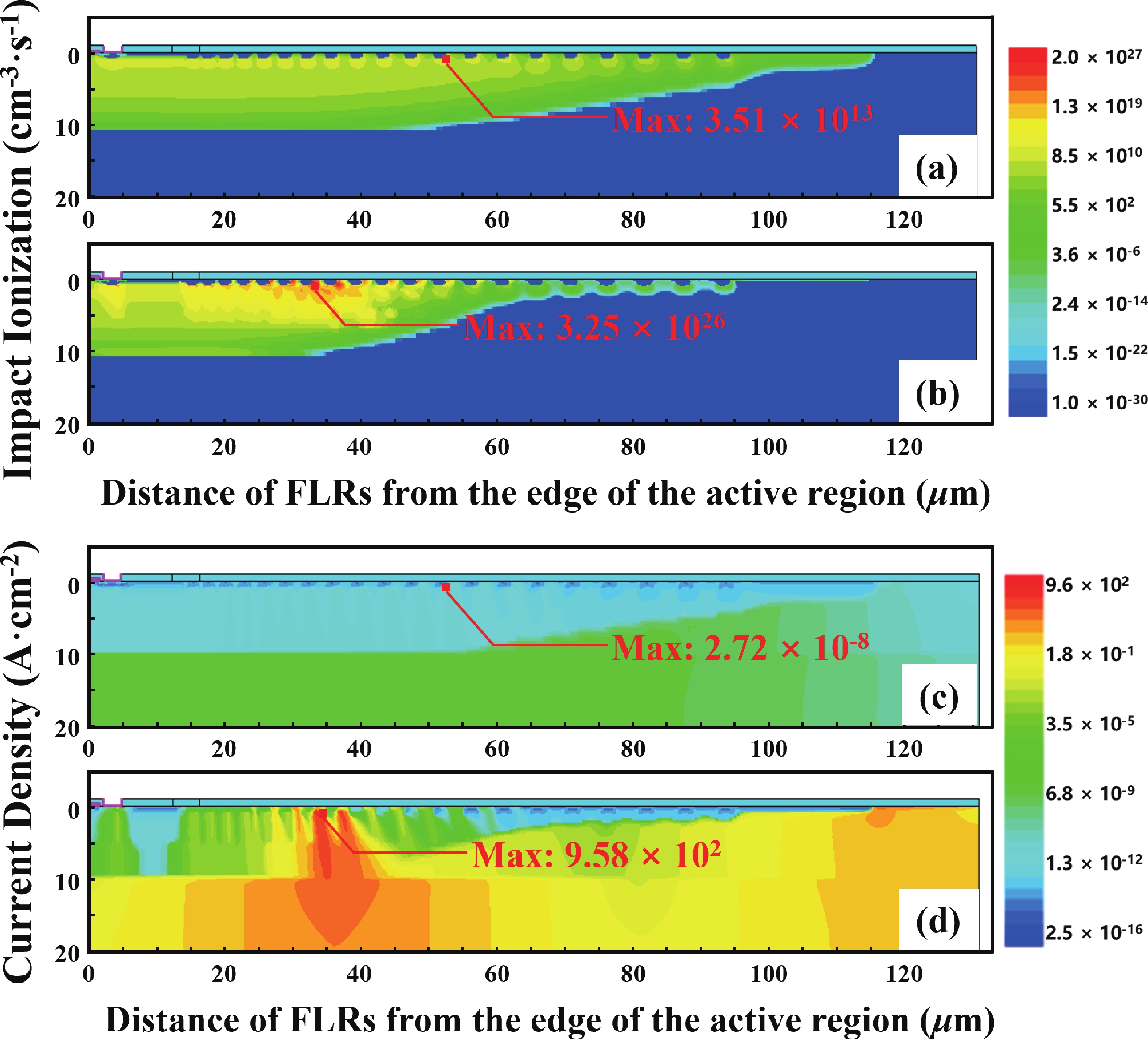
High gate oxide electric field, which can lead to device failure, is a common issue in SiC MOSFETs. To mitigate this issue and ensure high device reliability, an electric field shielding layer (also called depletion layer) in JFET region is always used to reduce the gate oxide electric filed strength (Eox,max). However, there is still a lack of a detection methods to characterize the changes in the depletion layer of the JFET region. In this paper, a type of 1200 V 4H-SiC MOSFET with different JFET widths and cell topologies is designed and fabricated, and an innovative detection method for the depletion layer of JFET region is proposed for the first time. This method is adopted to focus on discussing the influence of the depletion layer formed by different JFET widths on Vg, and the changes in the gate oxide capacitance Cg of hexagonal cells and linear cells during the formation of the JFET depletion layer are studied. Finally, the robustness of different cell topologies and JFET widths is determined by the depletion voltage drift in the high temperature gate reverse bias tests (HTGB−) reliability test.
J. Semicond.
2026, 47(4): 042301 doi: 10.1088/1674-4926/25090014
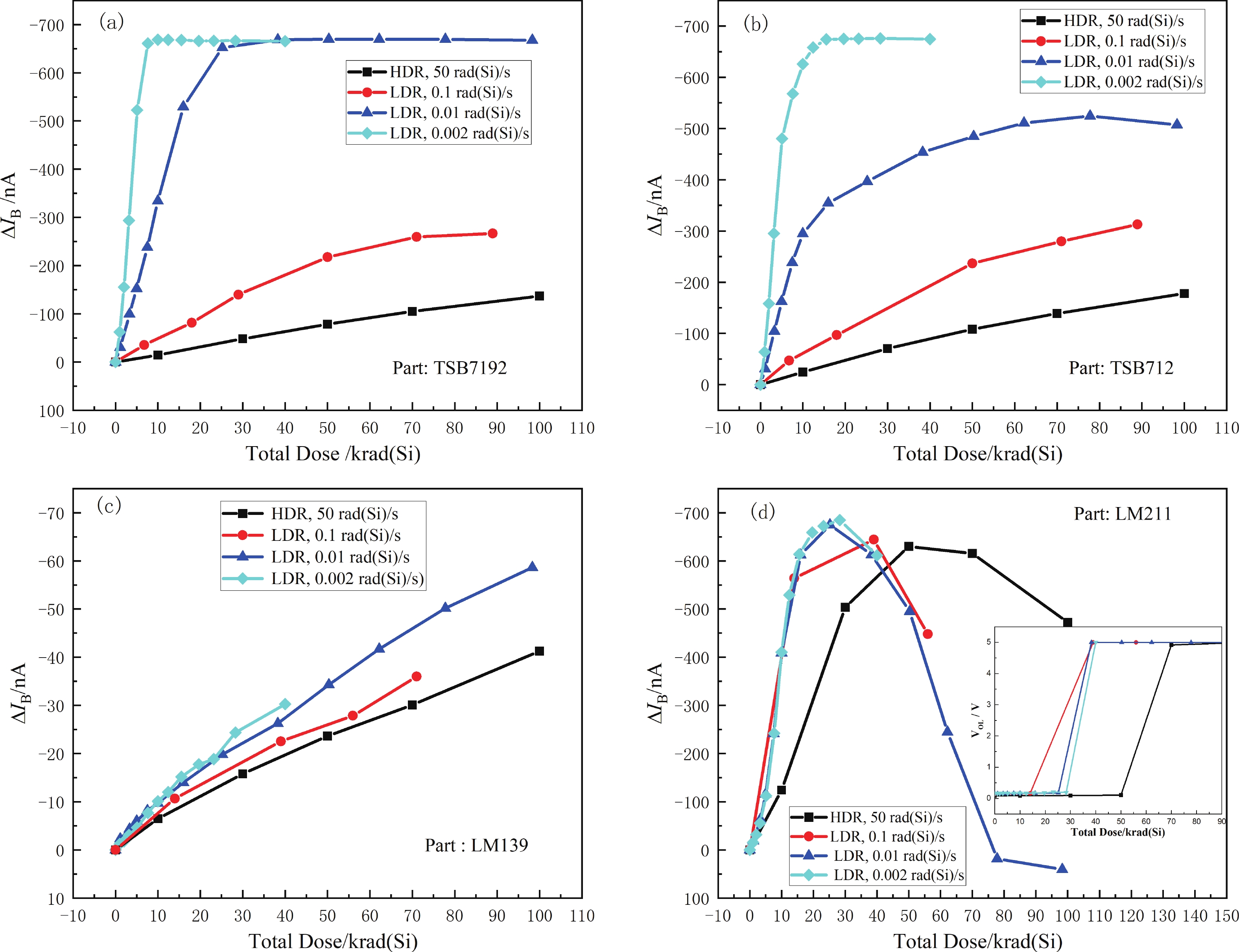
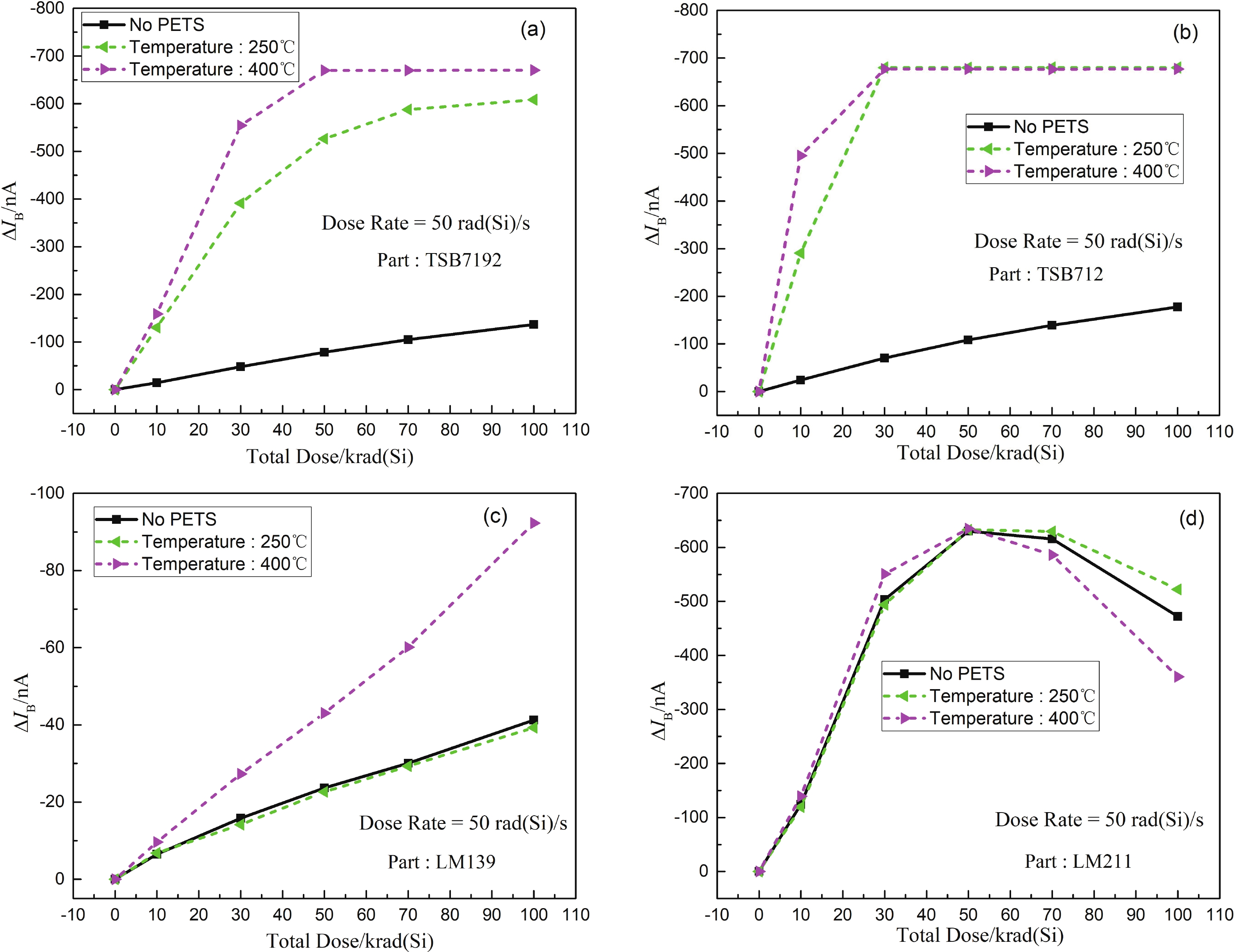
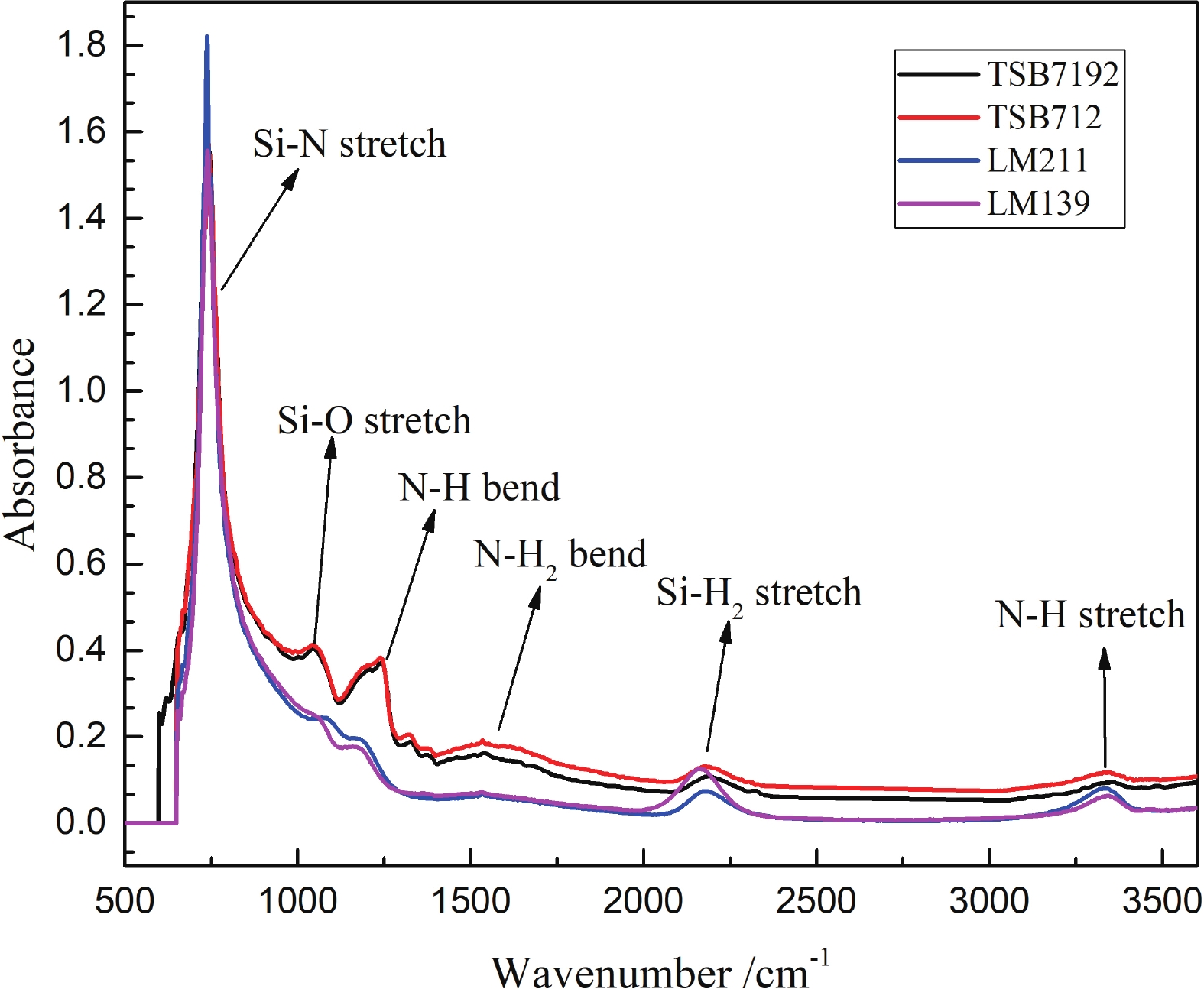
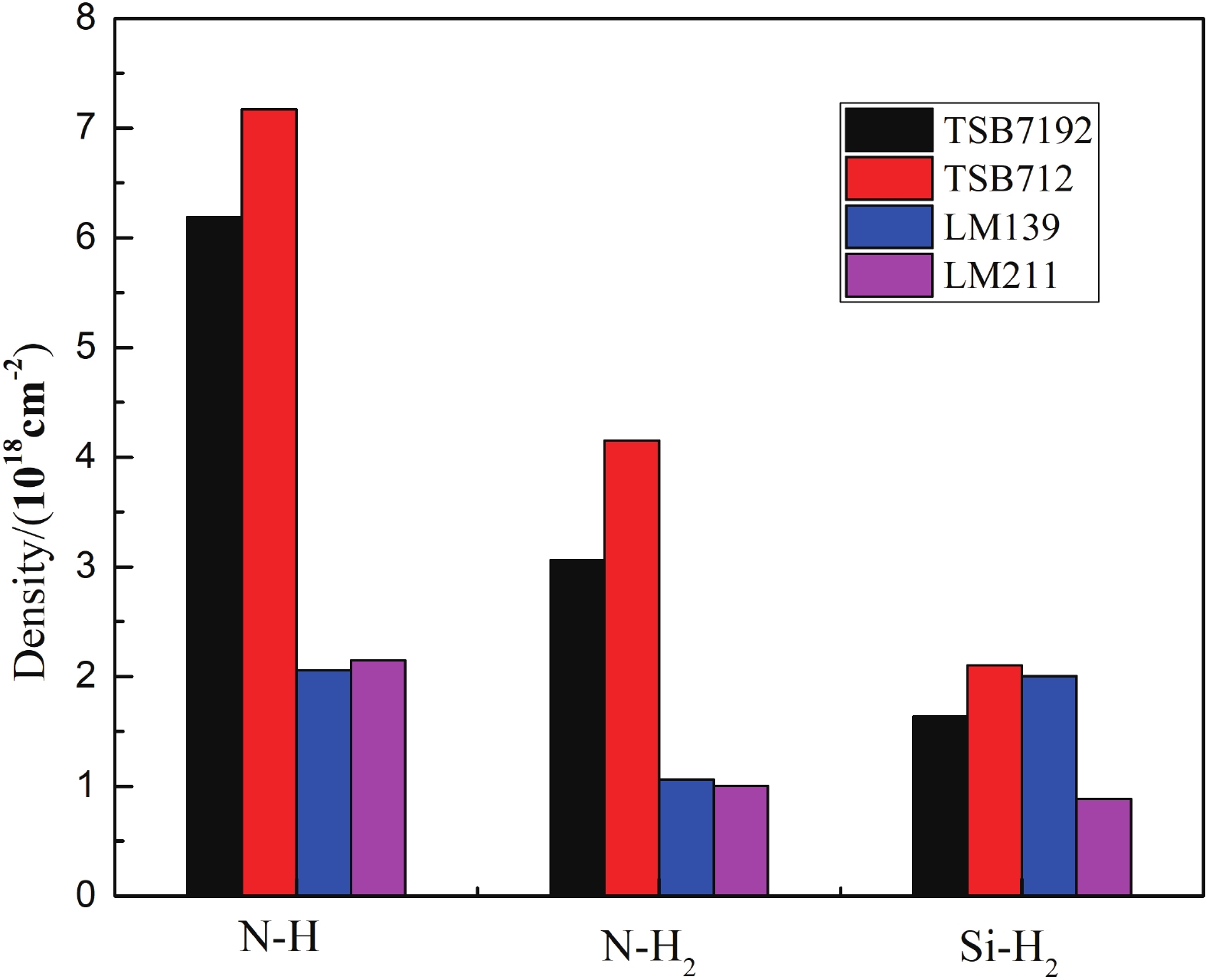
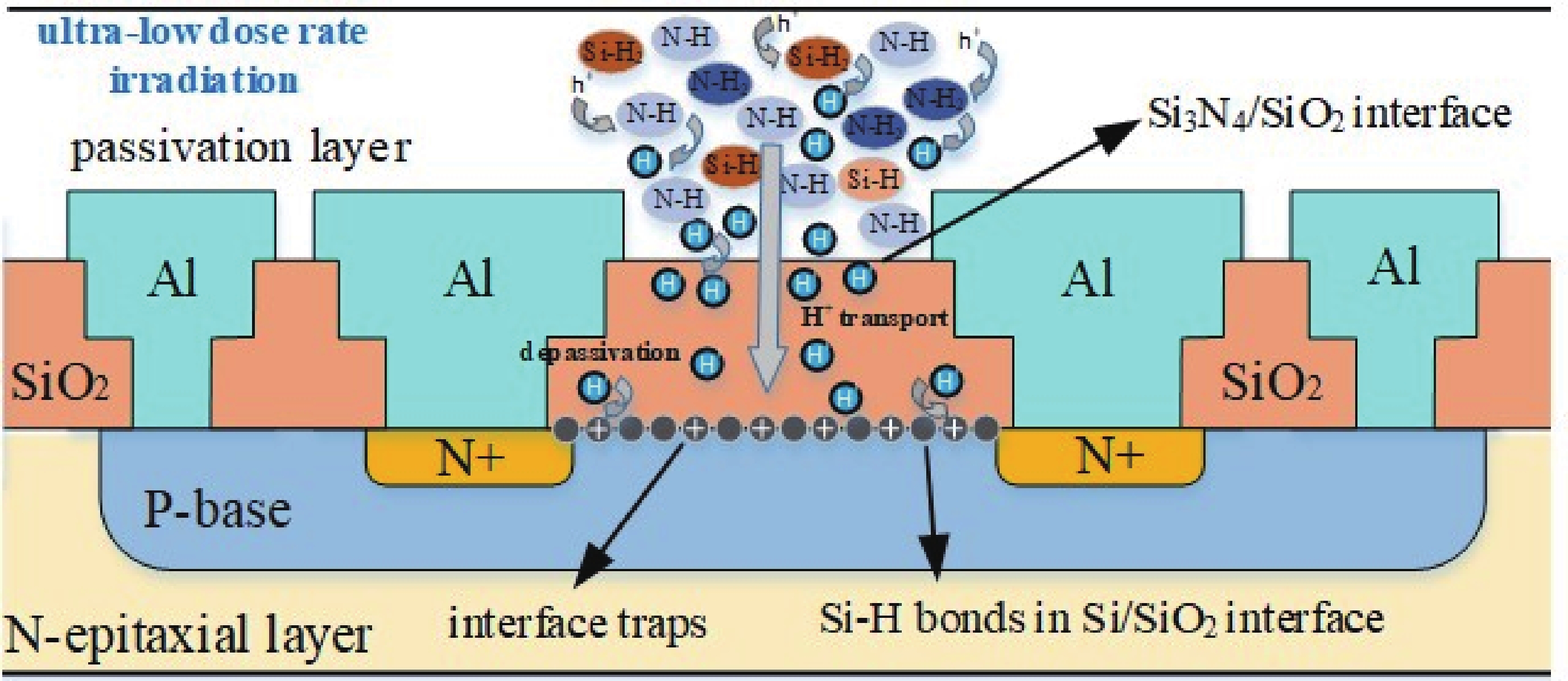
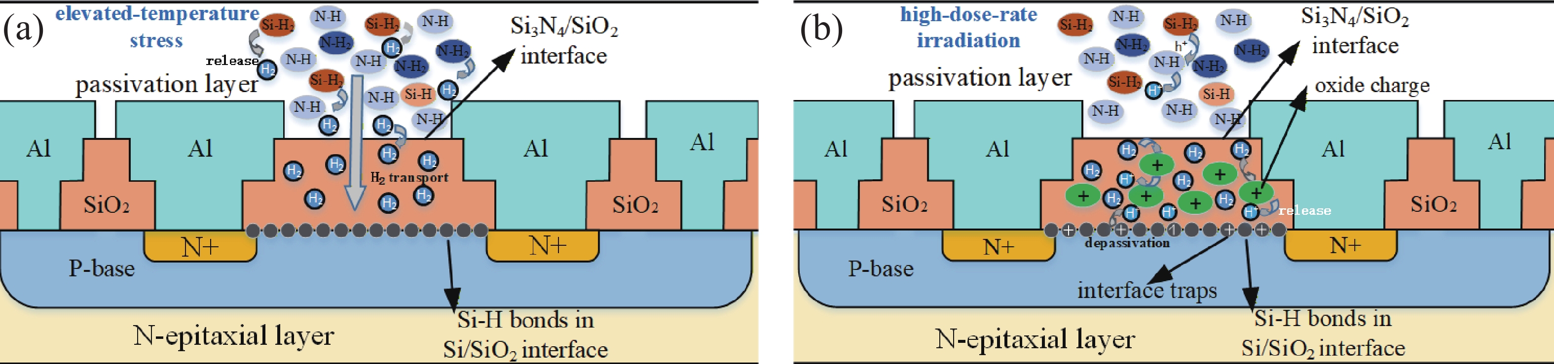
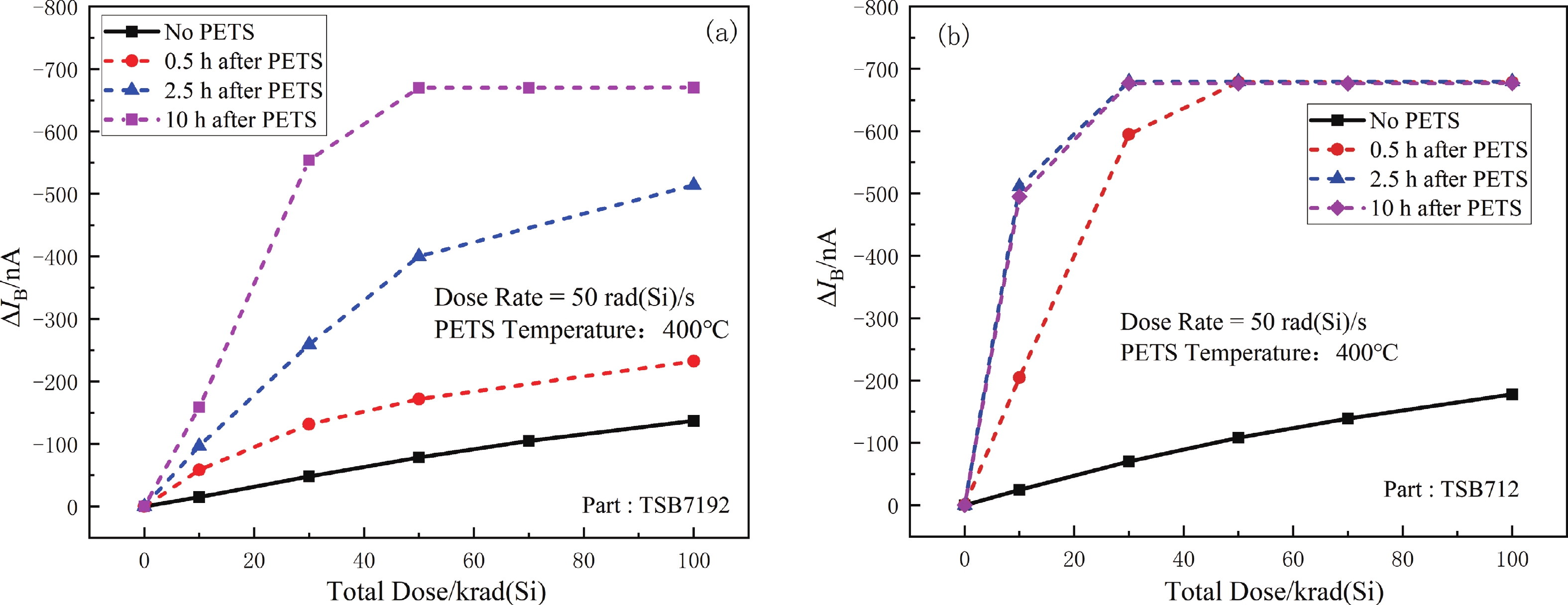
Enhanced low dose rate sensitivity (ELDRS) experiments were carried out on four commercial bipolar integrated circuits at dose rates ranging from 0.002 to 50 rad(Si)/s. Additionally, pre-irradiation elevated-temperature stress (PETS) experiments were conducted on the same devices at temperatures of 250 and 400 °C. The results show that for some devices, the radiation degradation when irradiated at an ultra-low dose rate of 0.002 rad(Si)/s is more than three times greater than that at a common low dose rate of 0.01 rad(Si)/s. Moreover, the maximum enhancement factor of the PETS effects reaches 20.3. It was also discovered that for devices exhibiting PETS effects, the saturation dose rate of ELDRS is less than 0.01 rad(Si)/s. A comprehensive analysis of the composition of the passivation layers indicated that the type and concentration of hydrogen bonds in these layers are the main factors contributing to the experimental outcomes.

J. Semicond.
2026, 47(4): 042302 doi: 10.1088/1674-4926/25080016

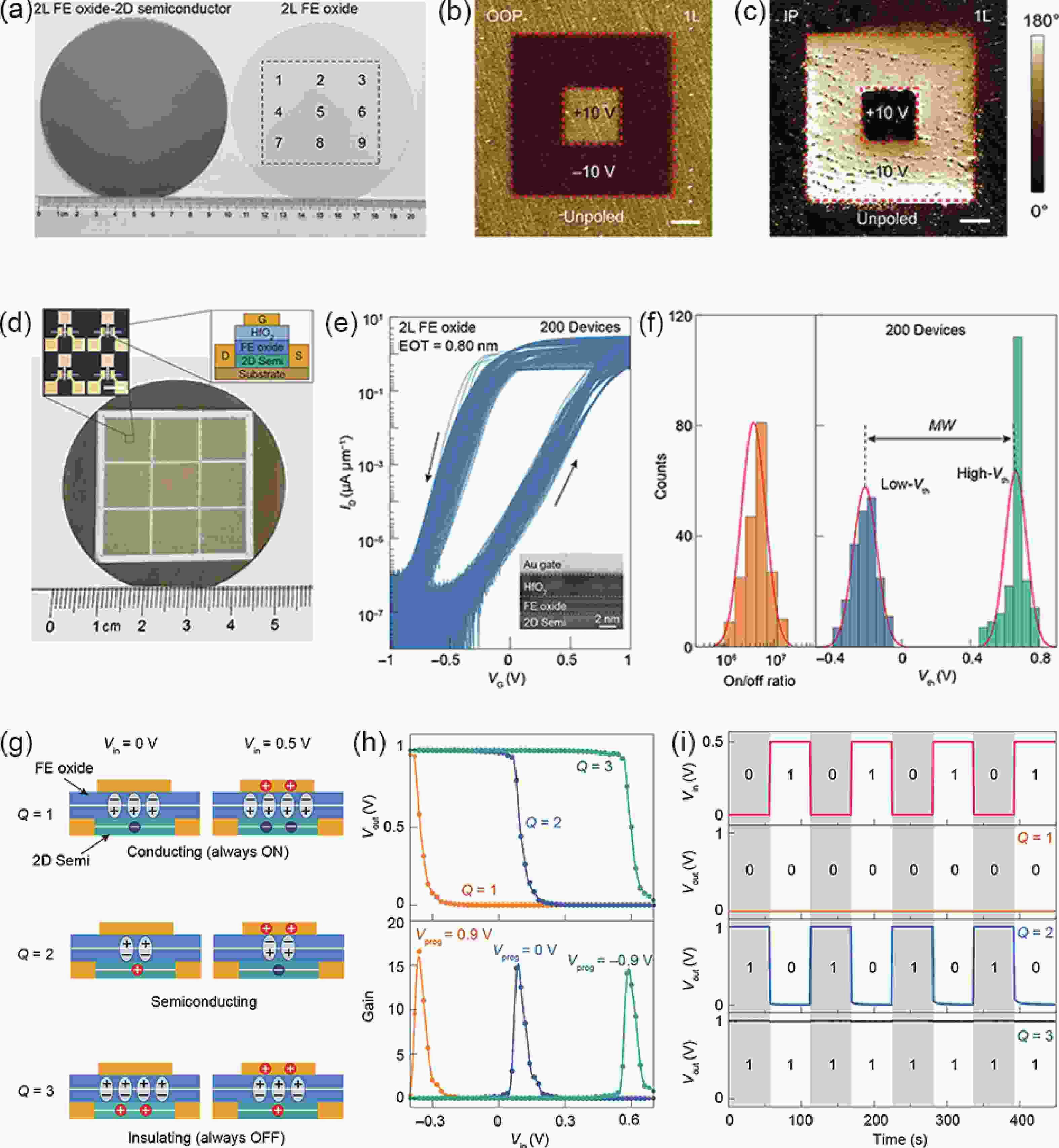
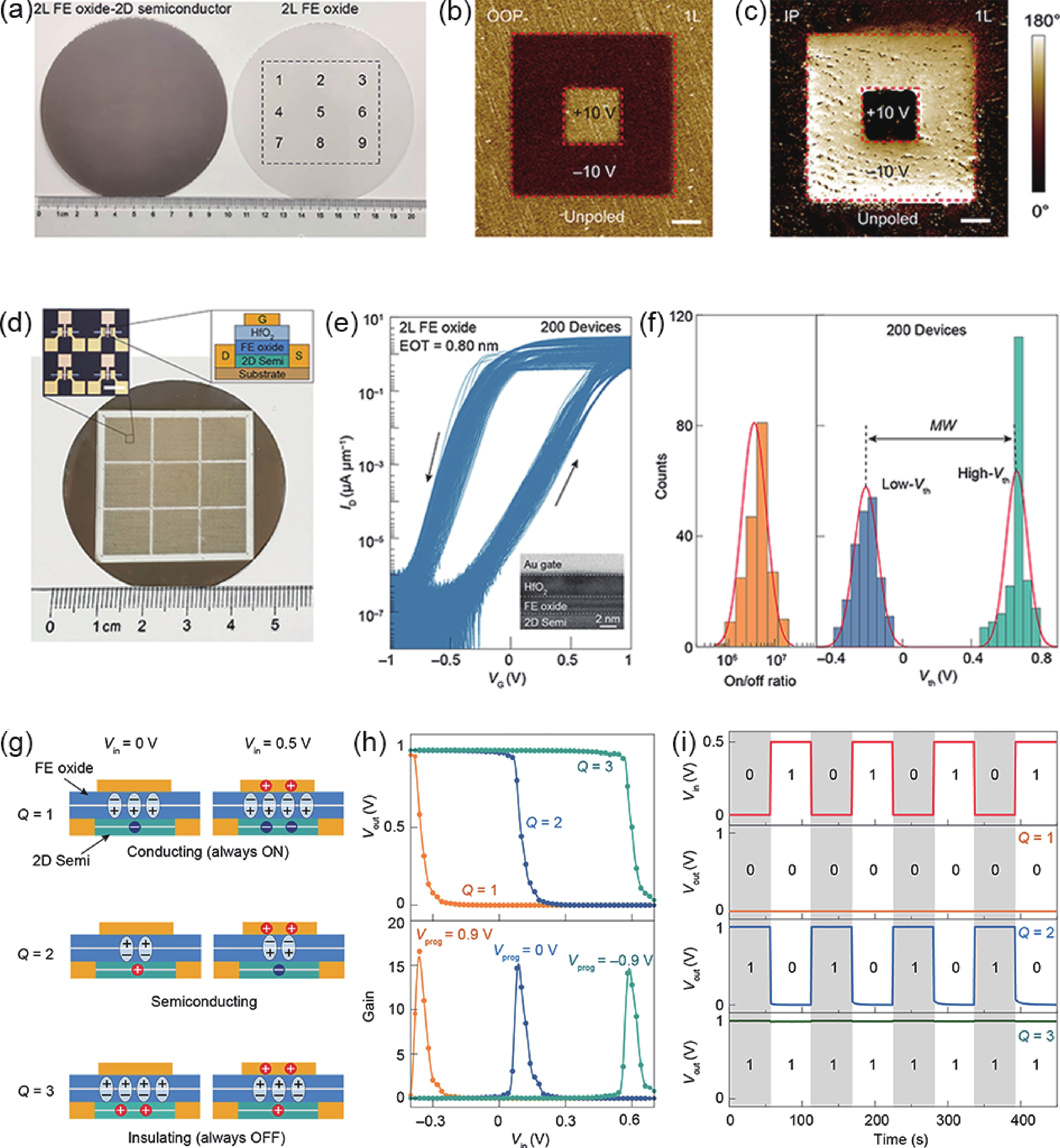
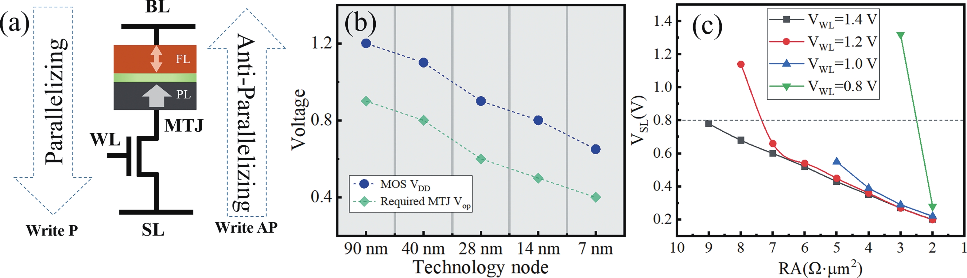
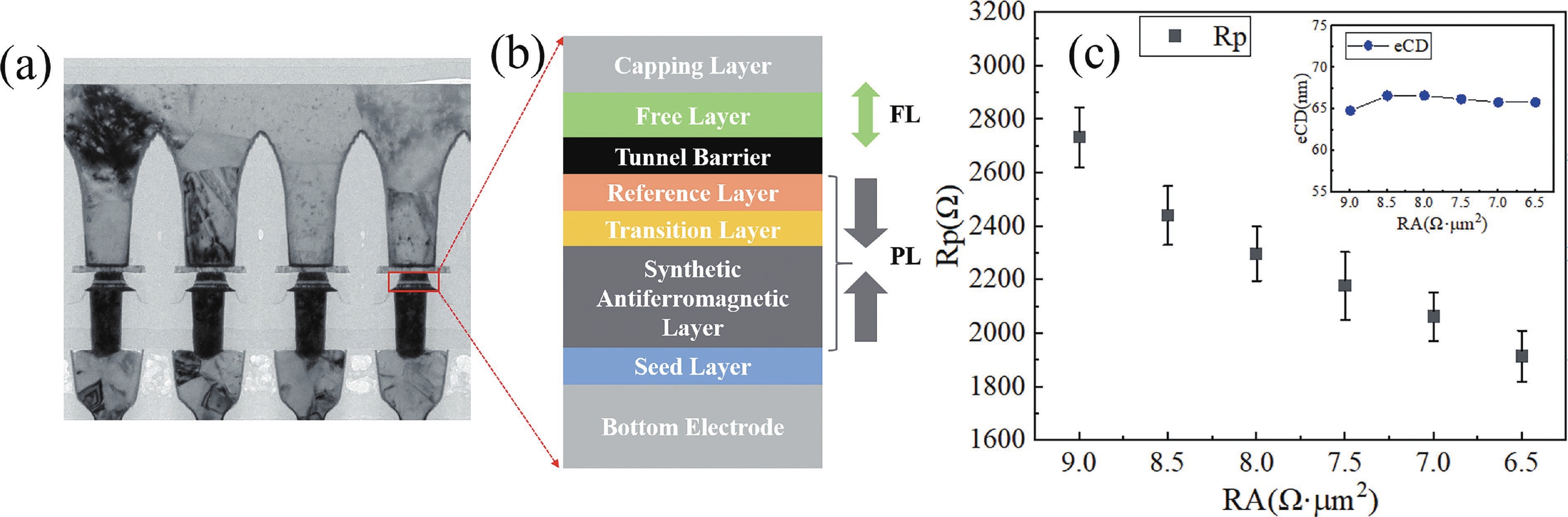
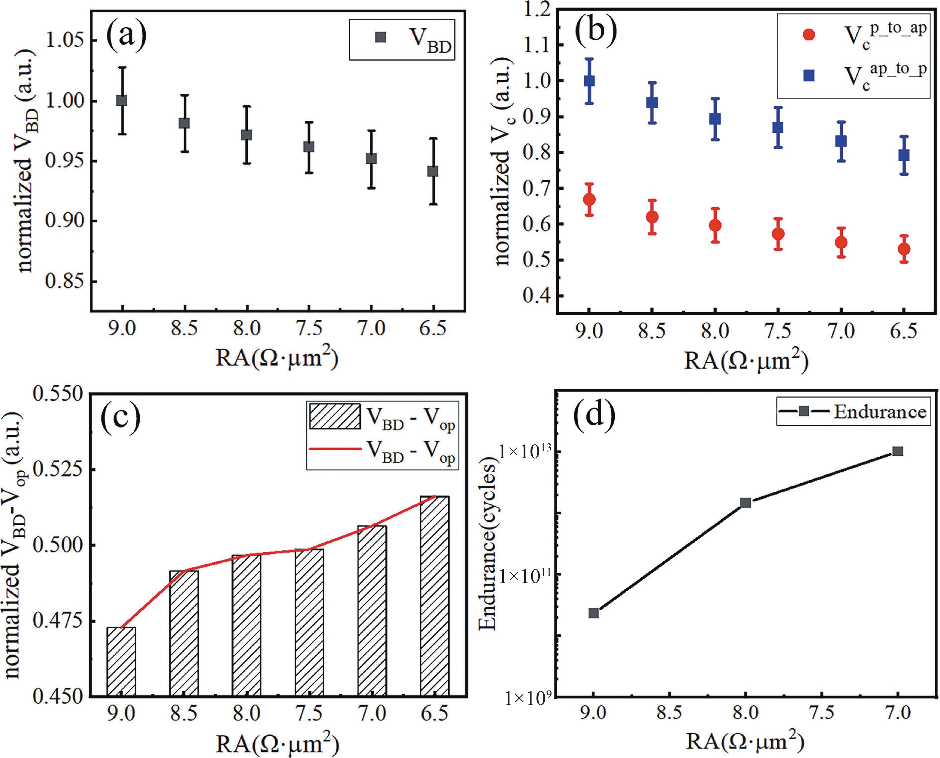
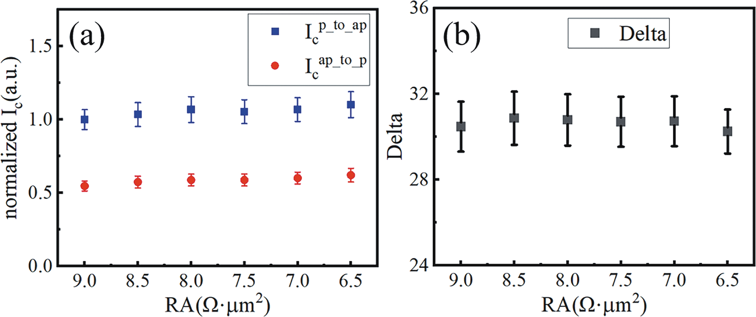
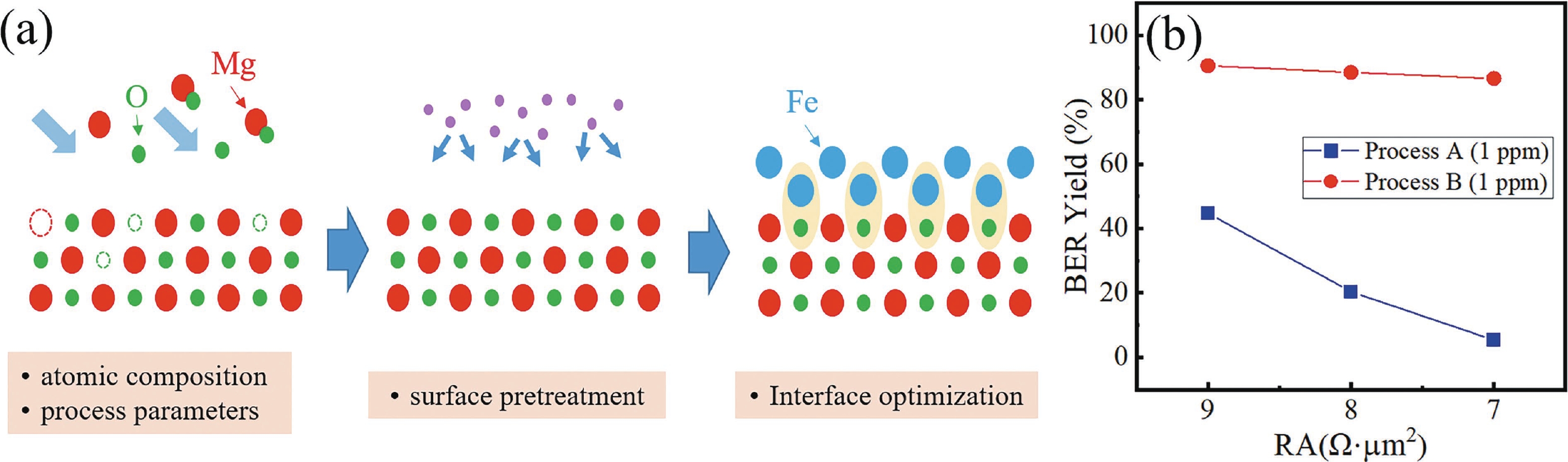
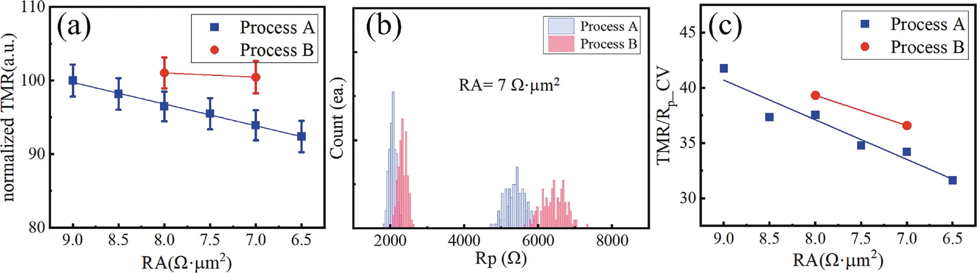
Spin-transfer-torque magnetic random-access memory (STT-MRAM), based on magnetic tunnel junctions (MTJs), is attracting significant attention for applications demanding high reliability and speed. To ensure high TMR which is essential for achieving sufficient sense margin, MTJs typically incorporate relatively thick tunnel barriers, resulting in high operating voltages. As the CMOS technology nodes advance and operating voltages decrease, reducing the MTJ switching voltage becomes imperative. However, MTJs with thinner tunnel barriers generally exhibit significantly degraded read margins and bit error rate, presenting a major challenge for achieving high-density, low-power MRAM. Here, we address this challenge through MgO tunnel barrier engineering and process optimization, successfully reducing the required MOS driving voltage while simultaneously expanding the write margin. Meanwhile, 85% array yield with sub-parts-per-million bit error rates at RA = 7 Ω·μm2 is achieved. These advancements are promising for developing high-density MRAM at advanced technology nodes.
J. Semicond.
2026, 47(4): 042303 doi: 10.1088/1674-4926/25070035
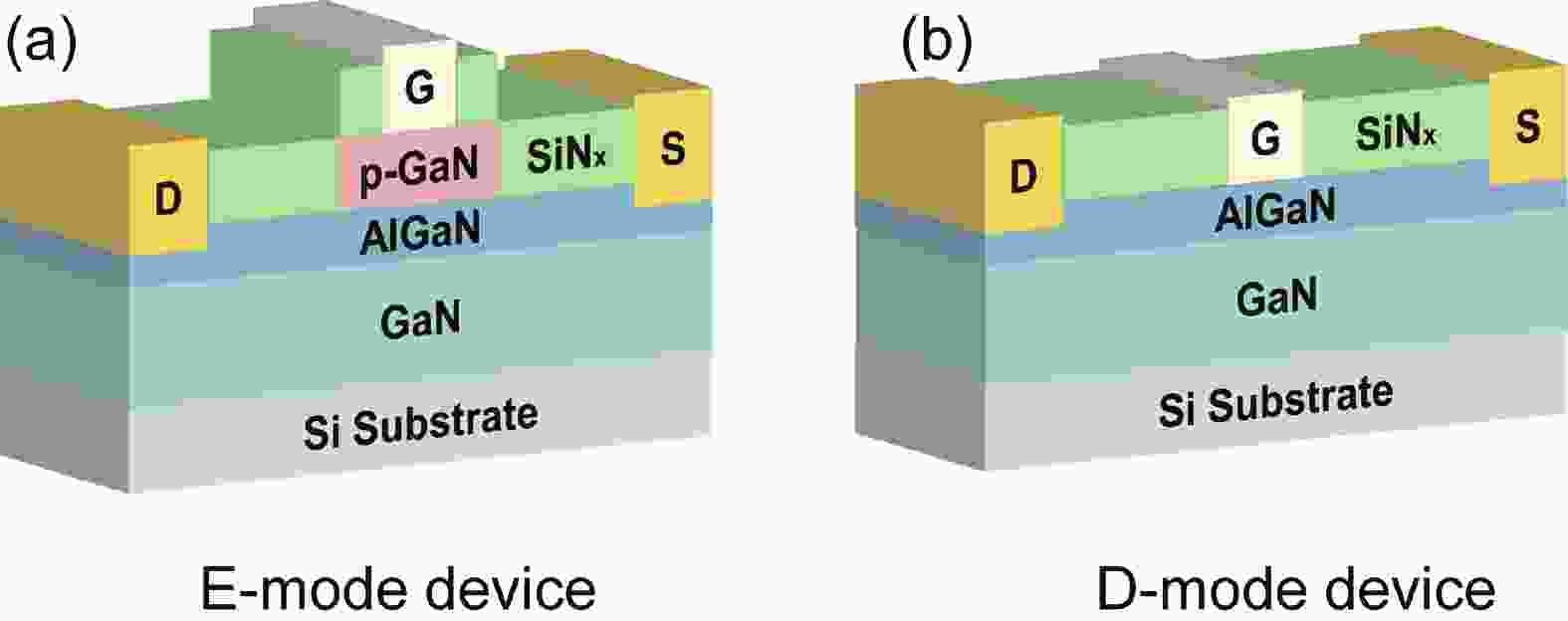
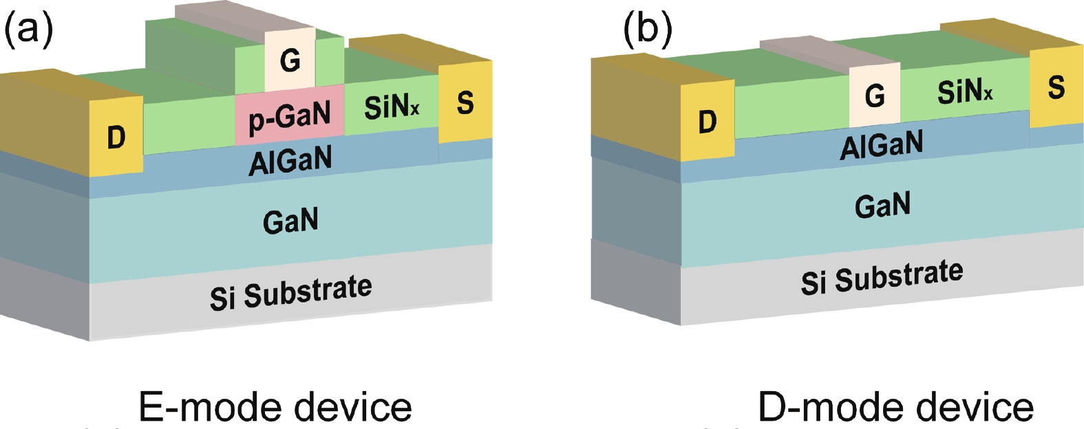
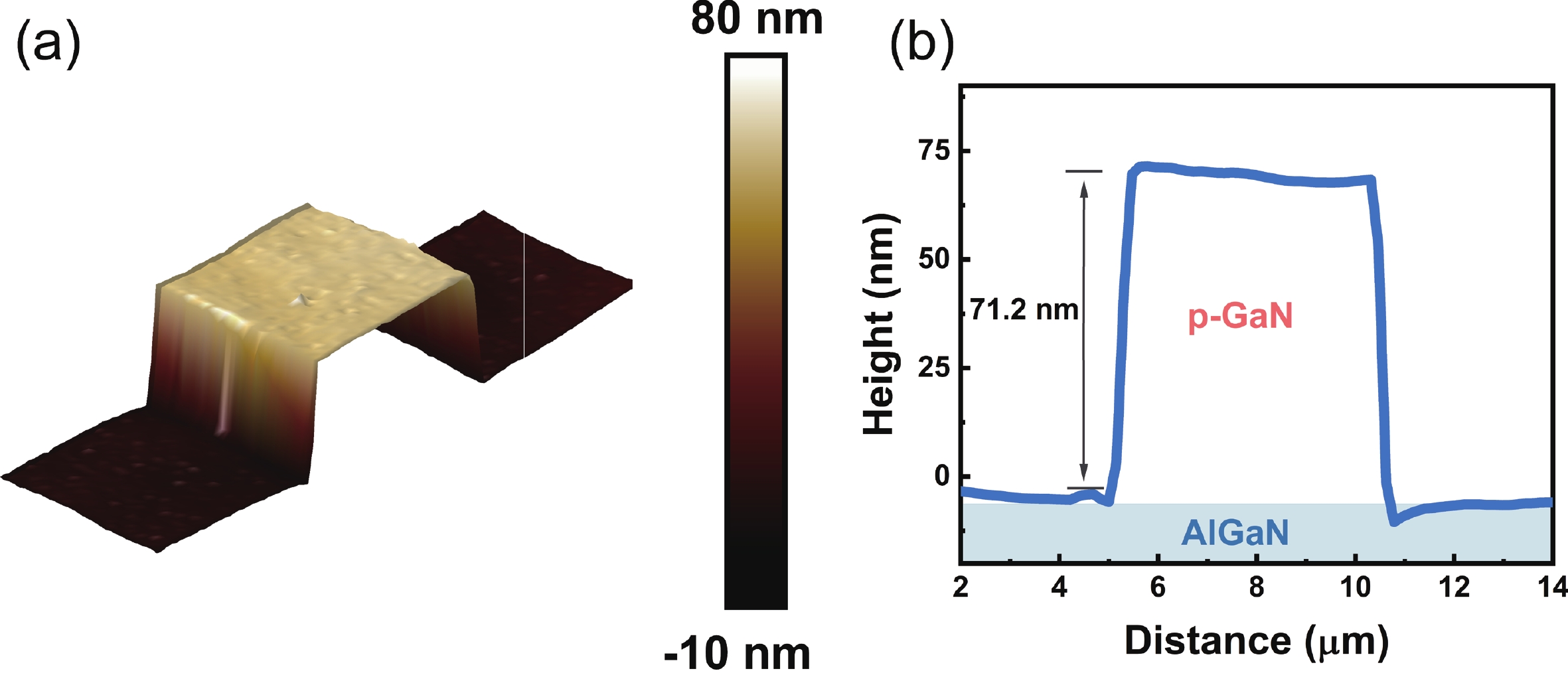
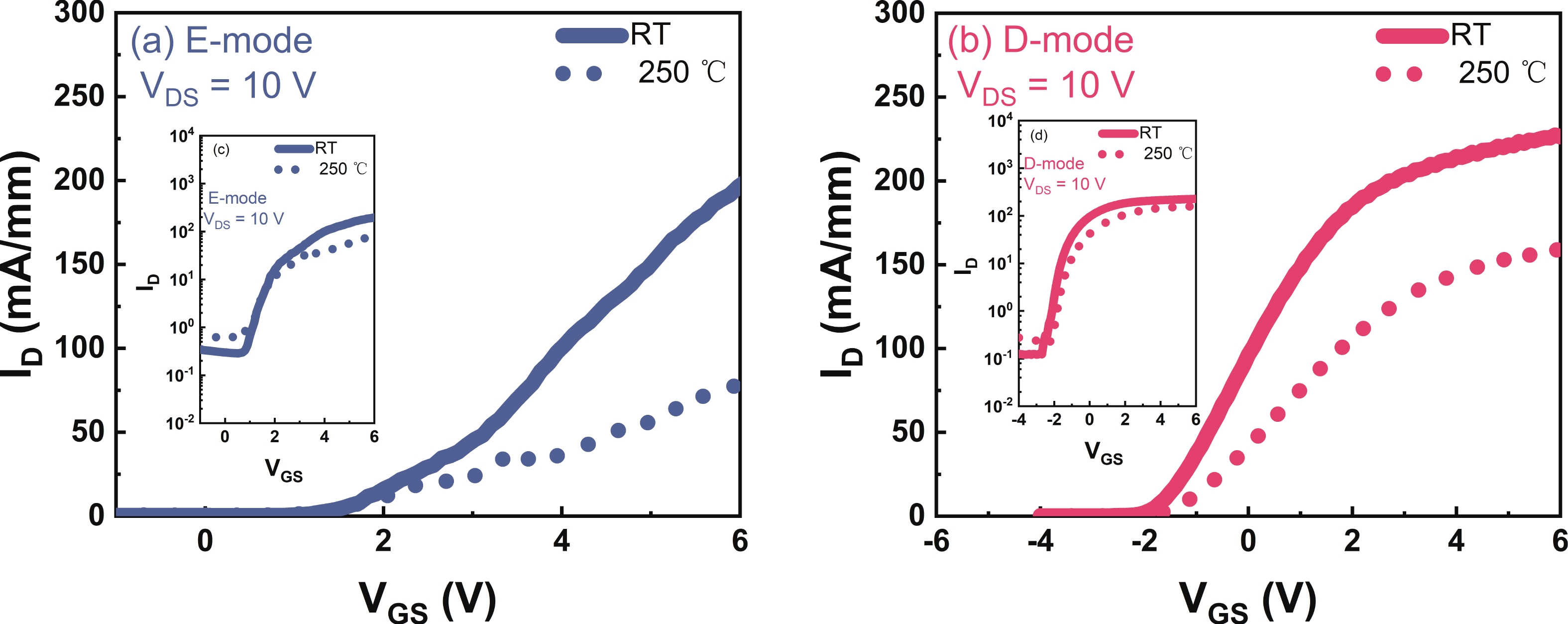
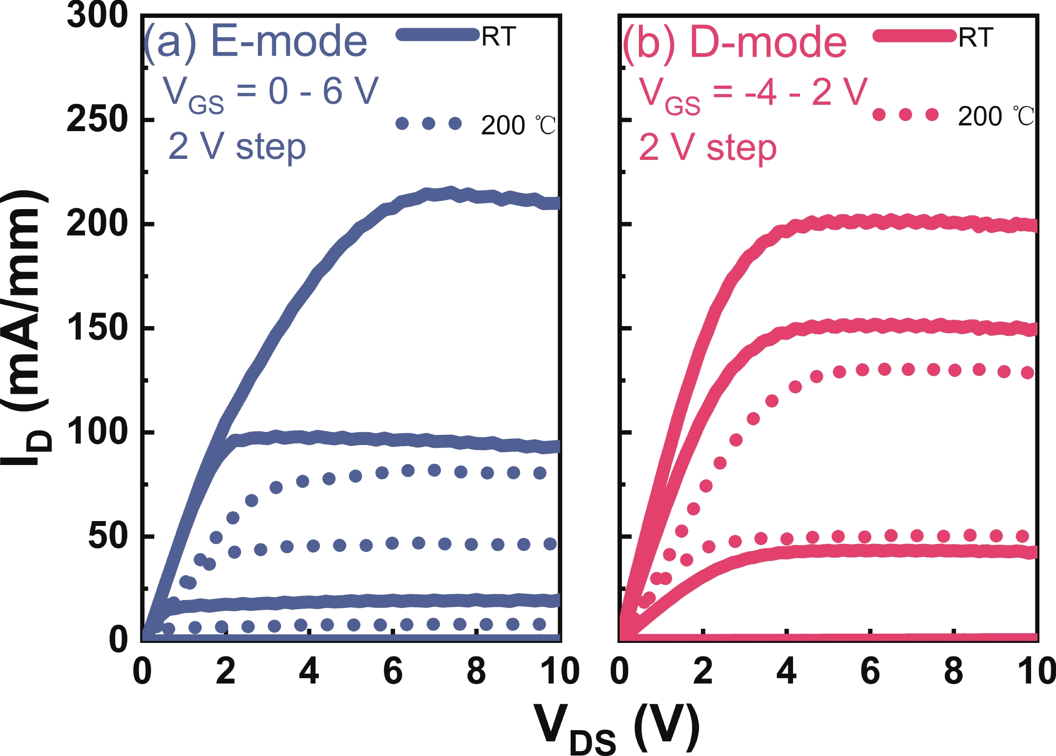
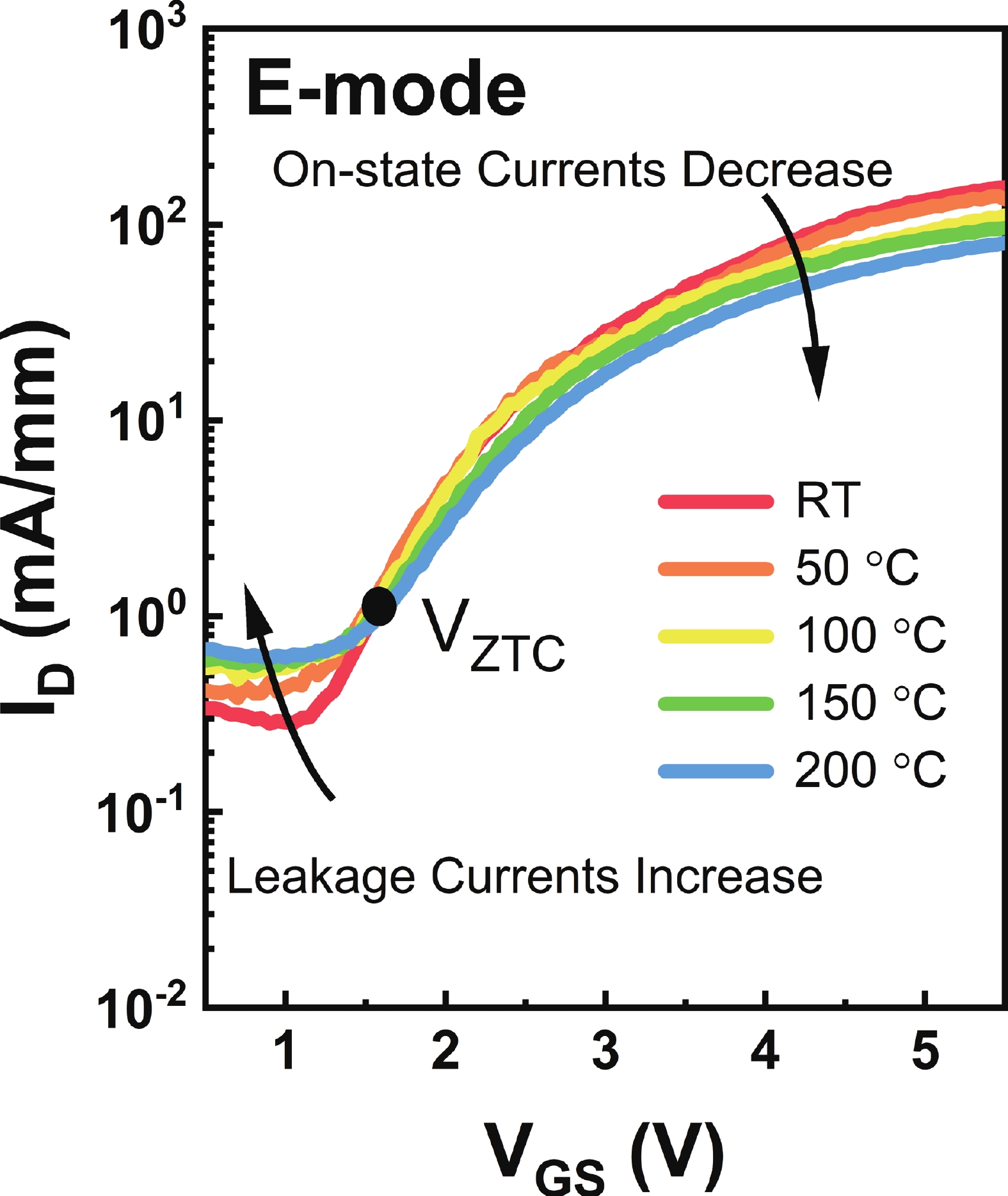
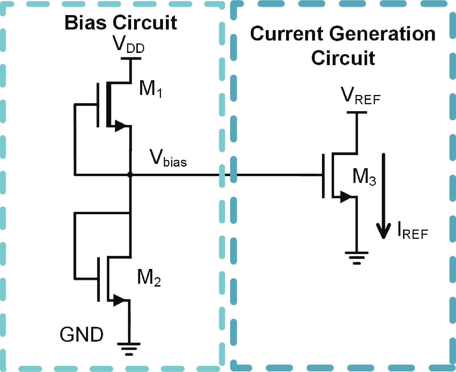
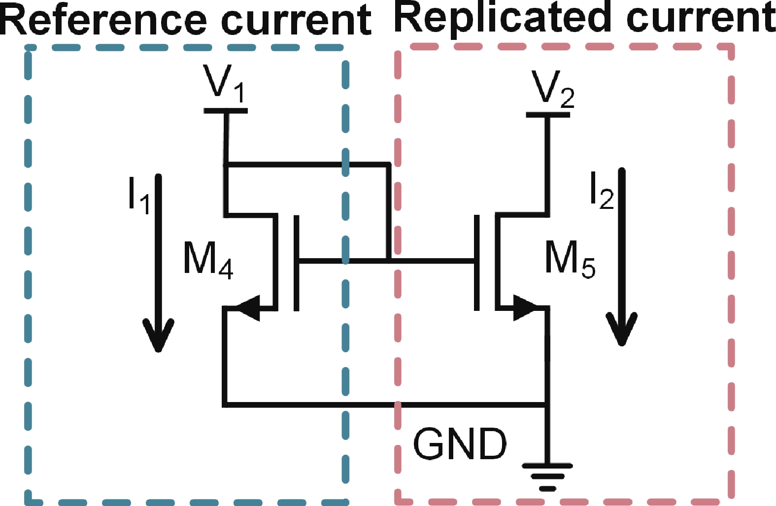
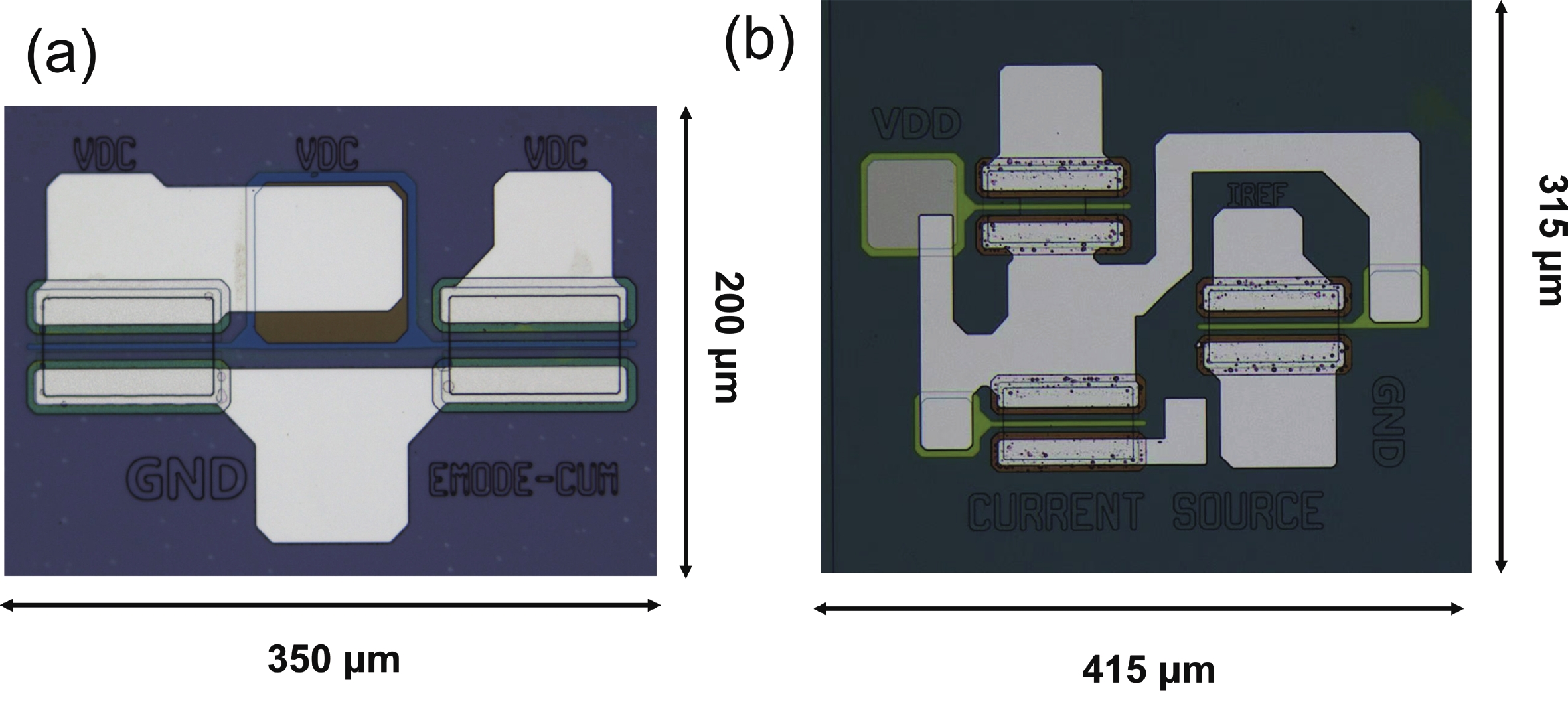
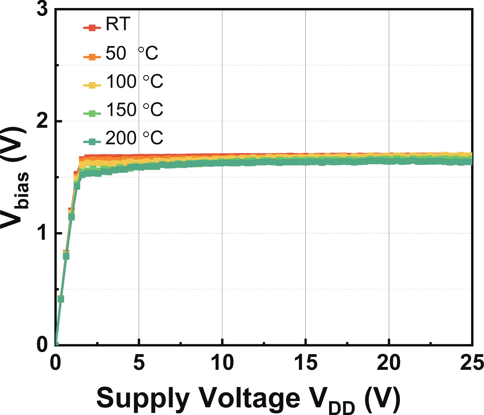
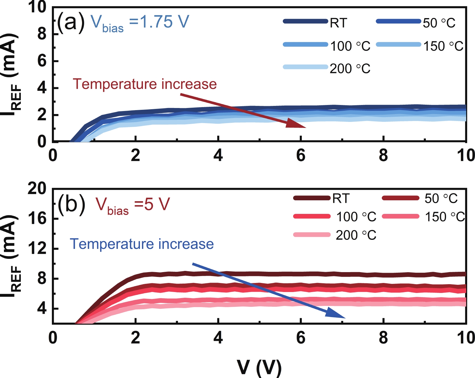
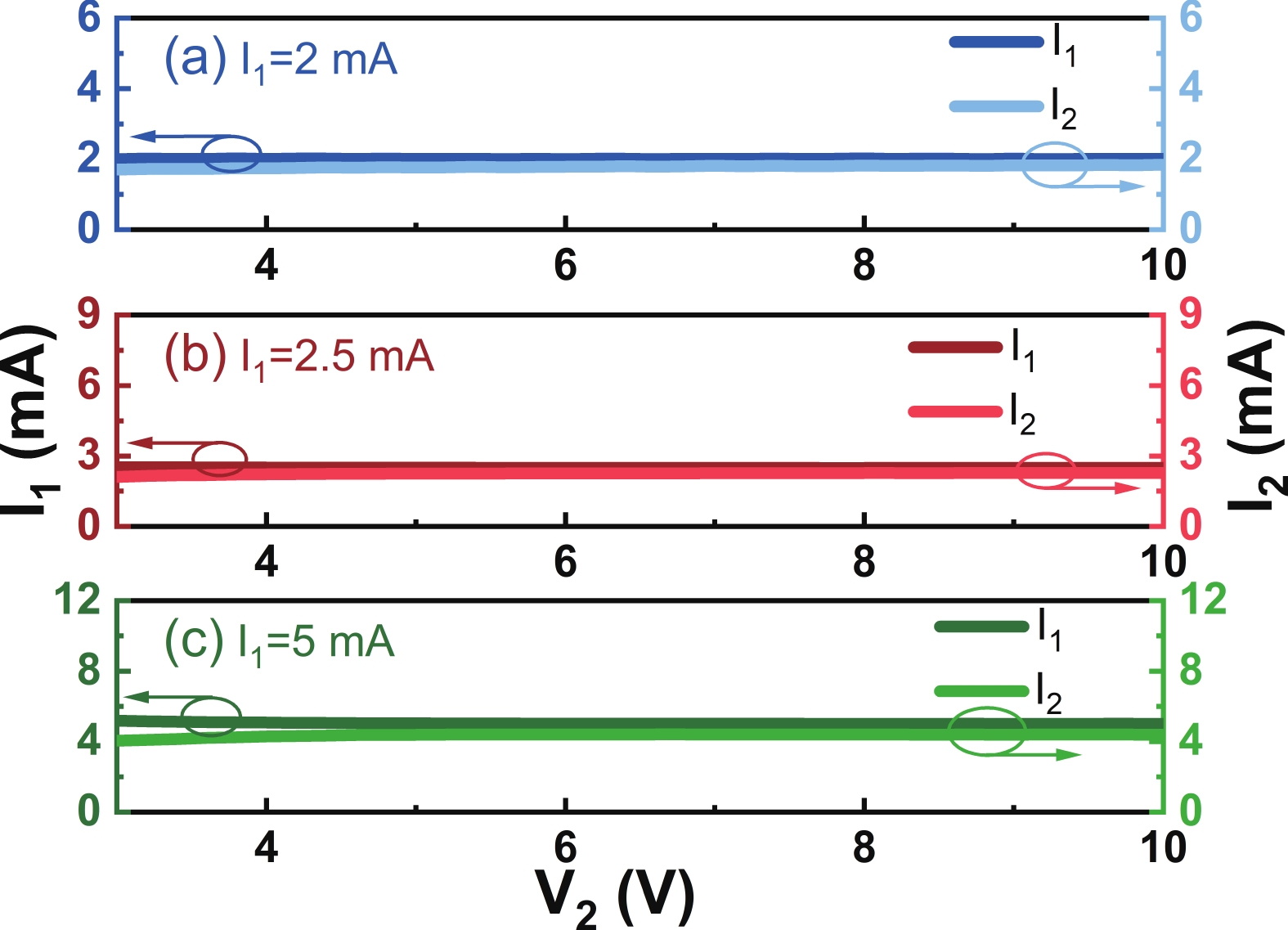
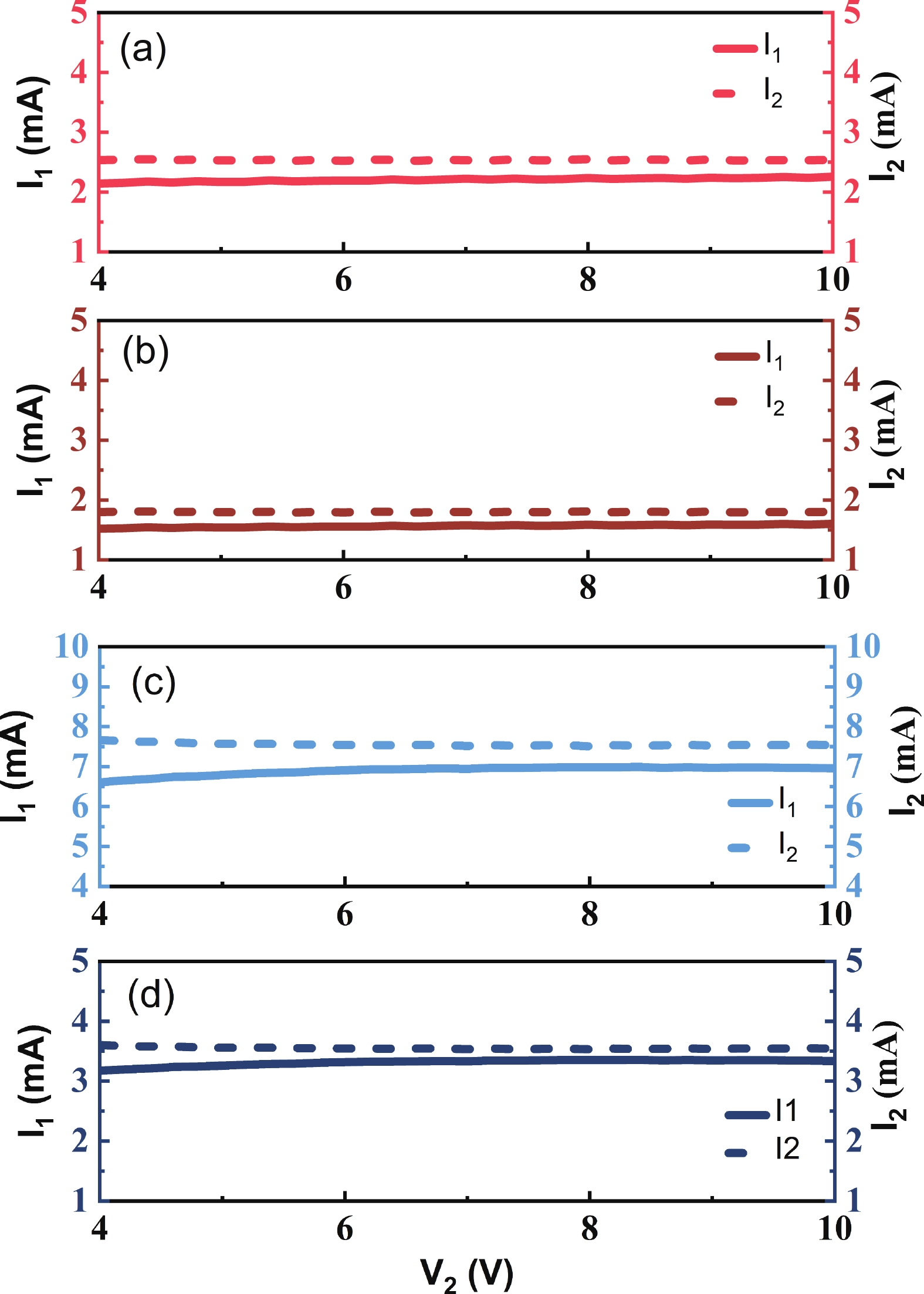
This paper demonstrates a monolithically integrated current reference and current mirror based on p-GaN gate HEMT technology, designed for high-temperature applications. The p-GaN current reference is composed of one D-mode and two E-mode devices. The generated reference current is independent of supply voltage since the proposed circuit incorporates a bias circuit capable of providing a supply-voltage-insensitive bias voltage. Moreover, under the zero-temperature coefficient (ZTC) bias voltage condition, the variation in the generated reference current at 200 °C is reduced by 15.4%, compared to a conventional p-GaN current reference with a bias voltage of 5 V. Experimental results indicate that the generated reference current slightly reduced from 2.53 to 1.70 mA over a broad temperature range of 25−200 °C. In addition, a current mirror circuit based on p-GaN HEMT technology was designed to imitate a reference current. The influence of temperature on the output current of the current mirror is mitigated, which could be realised by biasing the gate-to-source voltage at the zero-temperature coefficient voltage. This design sustains the current mirror mismatch error with small variation across a temperature range from room temperature to 200 °C. These results indicate that the GaN current reference and current mirror under zero-temperature coefficient bias voltage can ensure stable output current across different temperatures, facilitating the application of fully GaN integrated circuits in high-temperature environments.
J. Semicond.
2026, 47(4): 042304 doi: 10.1088/1674-4926/25070037
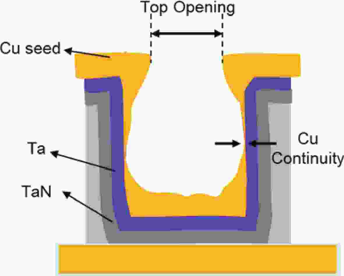
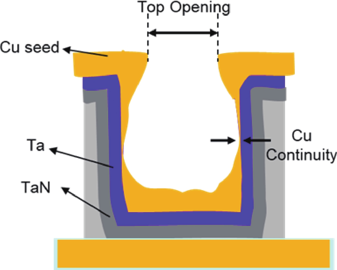
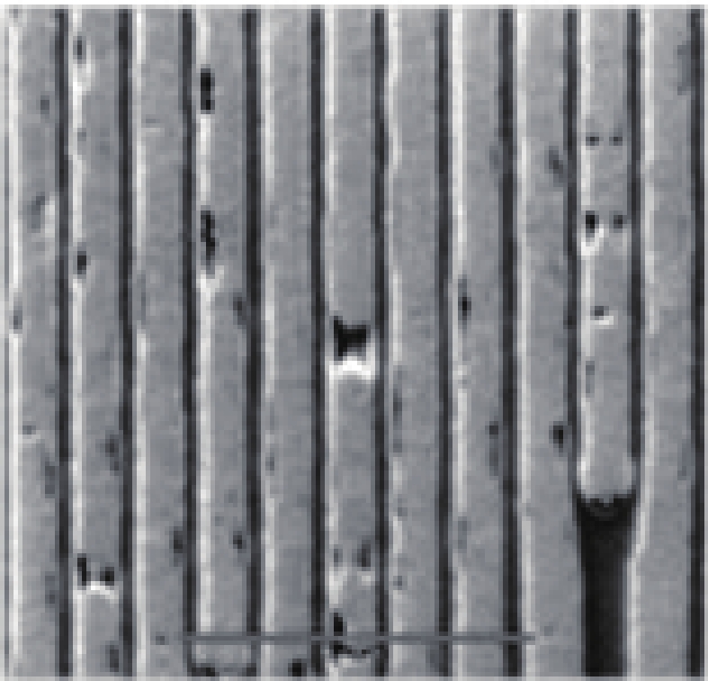
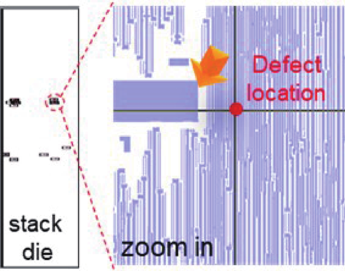
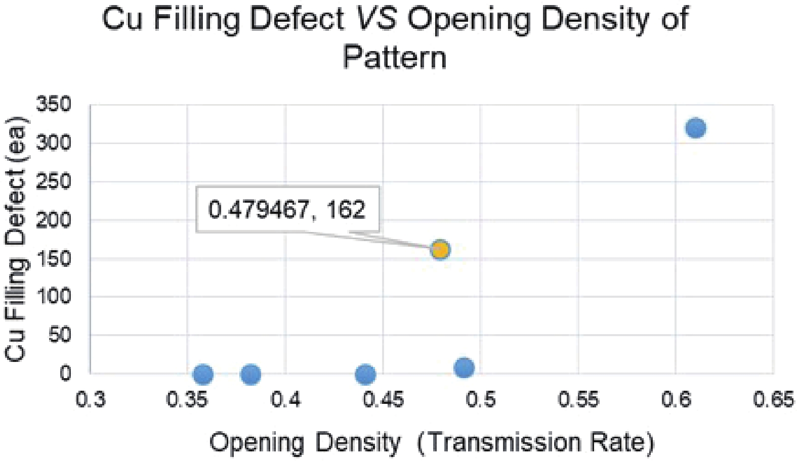
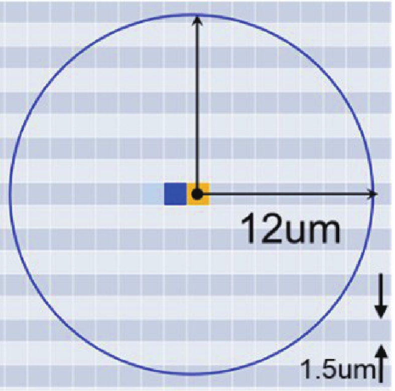
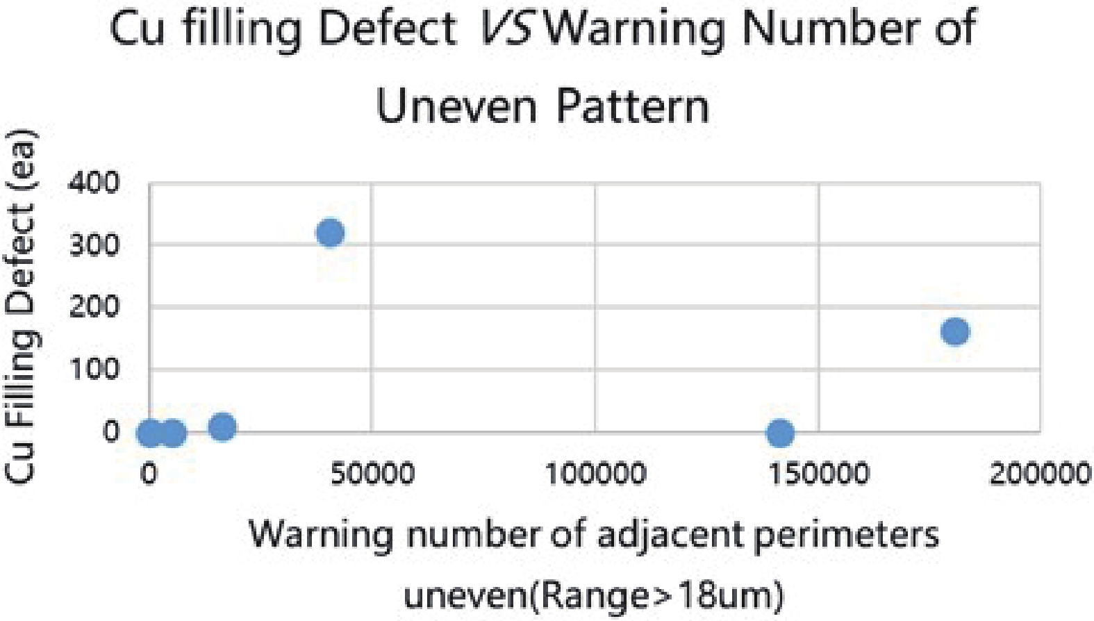
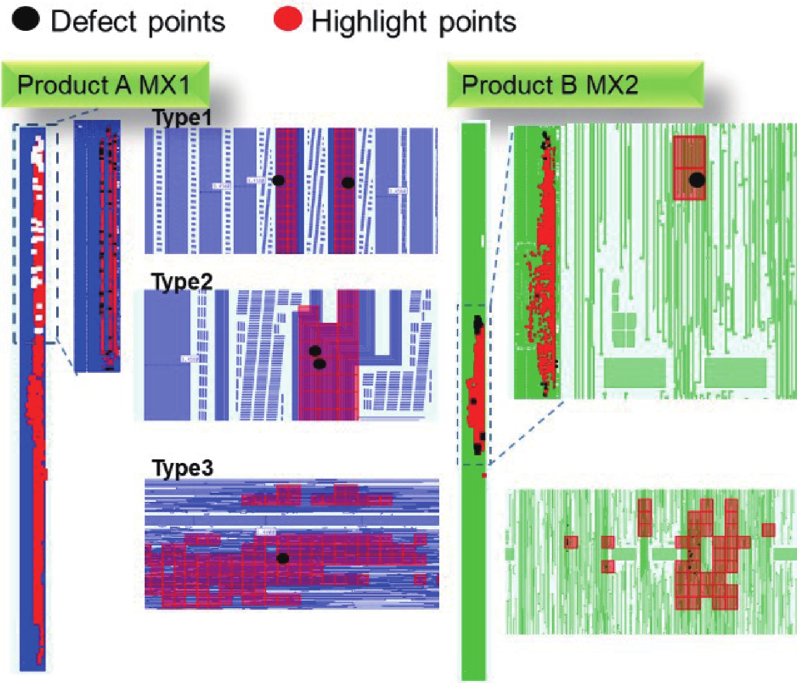
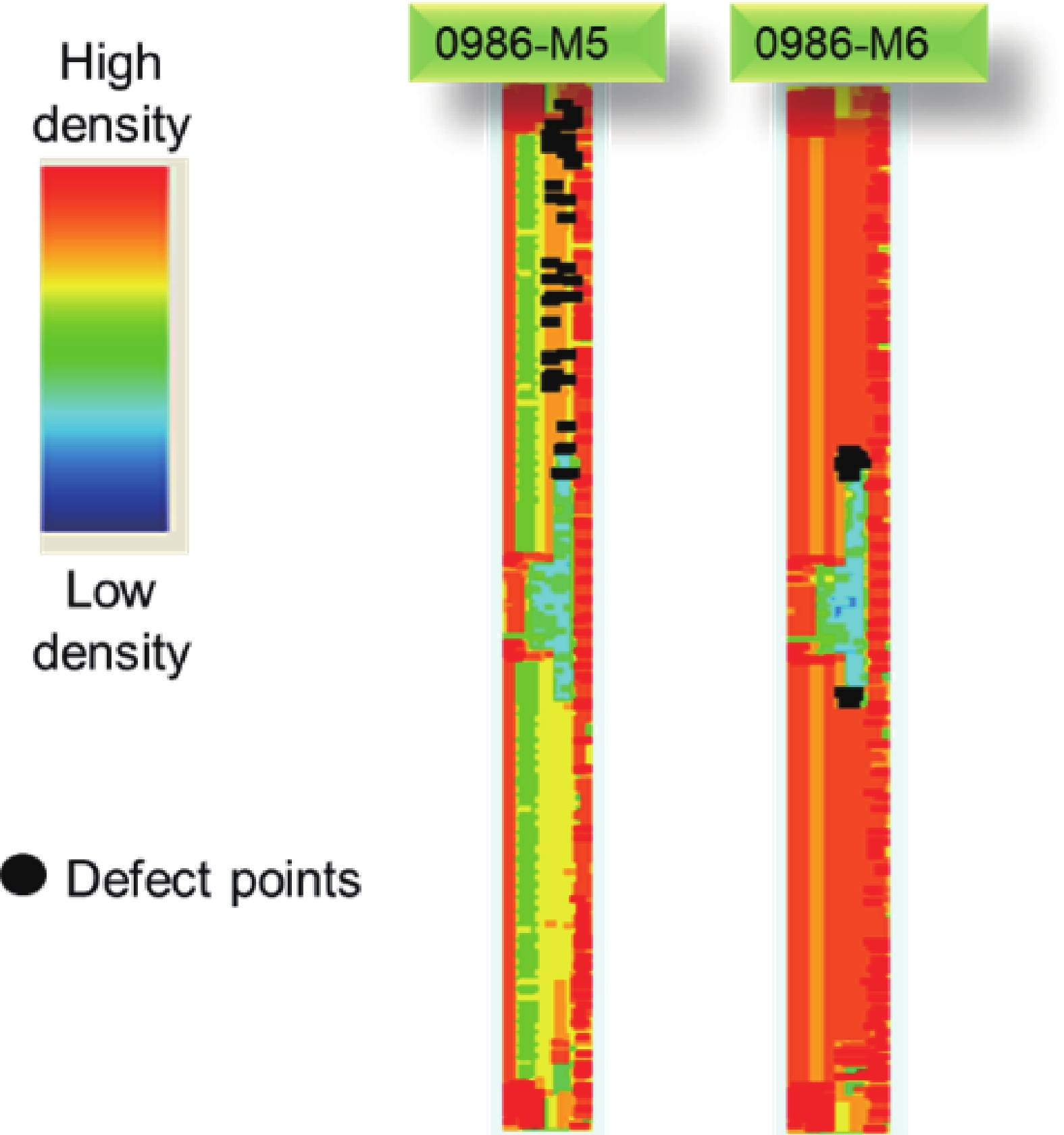
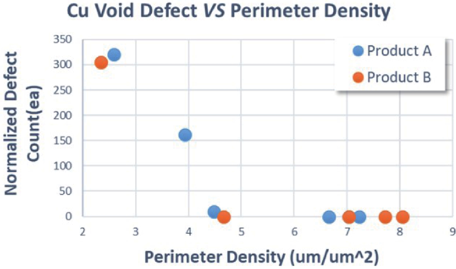
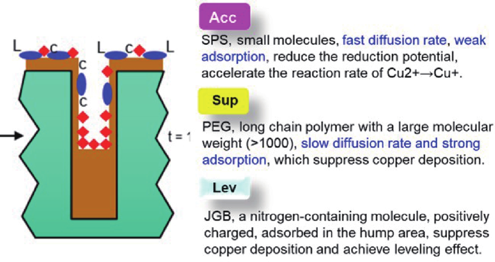
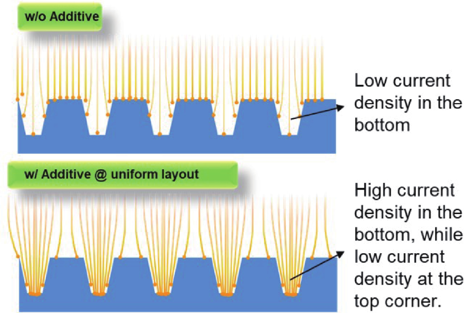
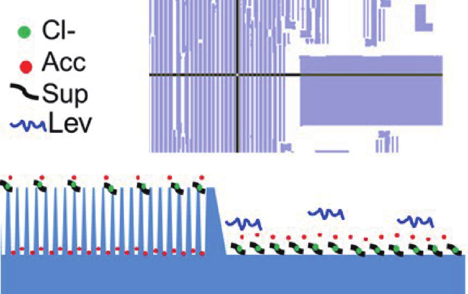
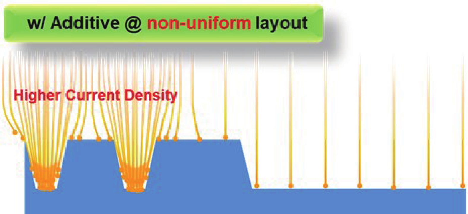
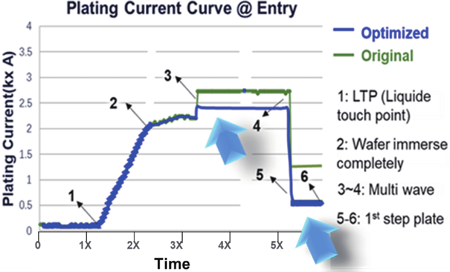
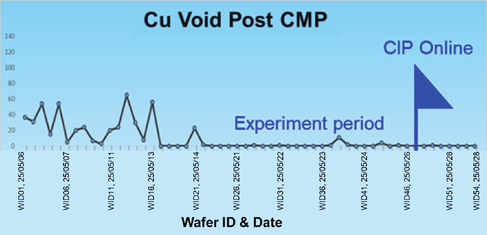
The downscaling of logic devices has posed numerous engineering and manufacturing challenges in copper (Cu) interconnections. The primary failure modes of Cu filling defects are narrow top openings and discontinuous Cu seeds on sidewalls. This study investigates the influence and mechanism of layout on Cu filling defects. Dense line wires with uneven local layouts are prone to defects, which is attributed to the altered distribution of additives in electrochemical plating (ECP), leading to differences in bottom-up filling behavior. It is demonstrated that large-sized metal conductor regions adjacent to dense line wires adsorb substantial amounts of suppressor, resulting in sparse current density in these areas. Given the fixed total local current density, the sparseness of current density in adjacent regions inevitably diverts more current lines to the dense line wire areas. The excessive current density exceeds the local redistribution capacity of additives, causing premature sealing of trench tops and the formation of void defects. A low-current plating process significantly mitigates these defects but may compromise the protective capability of the Cu seed. Additionally, the perimeter density of the layout serves as an effective evaluation index.
J. Semicond.
2026, 47(4): 042305 doi: 10.1088/1674-4926/25100015

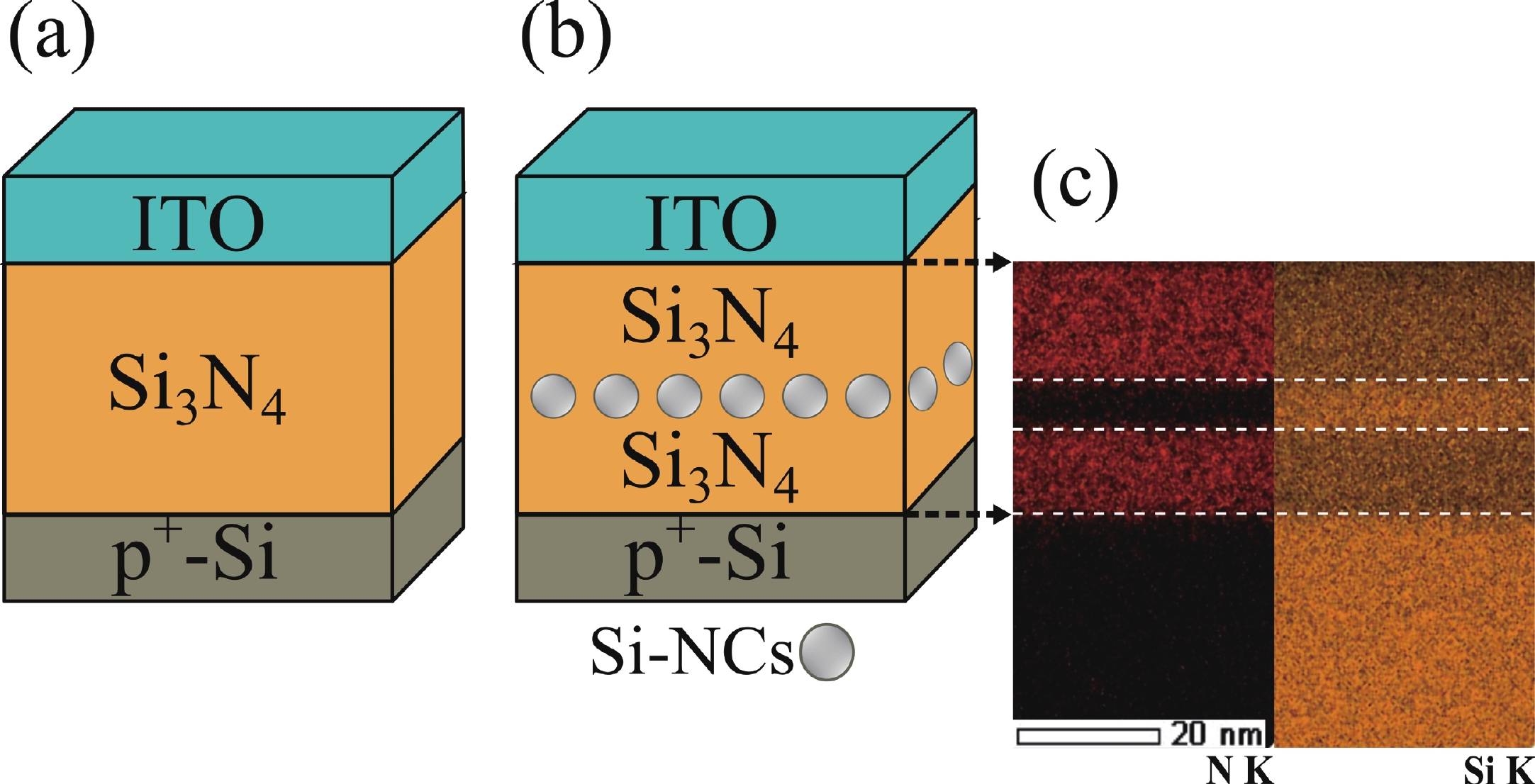
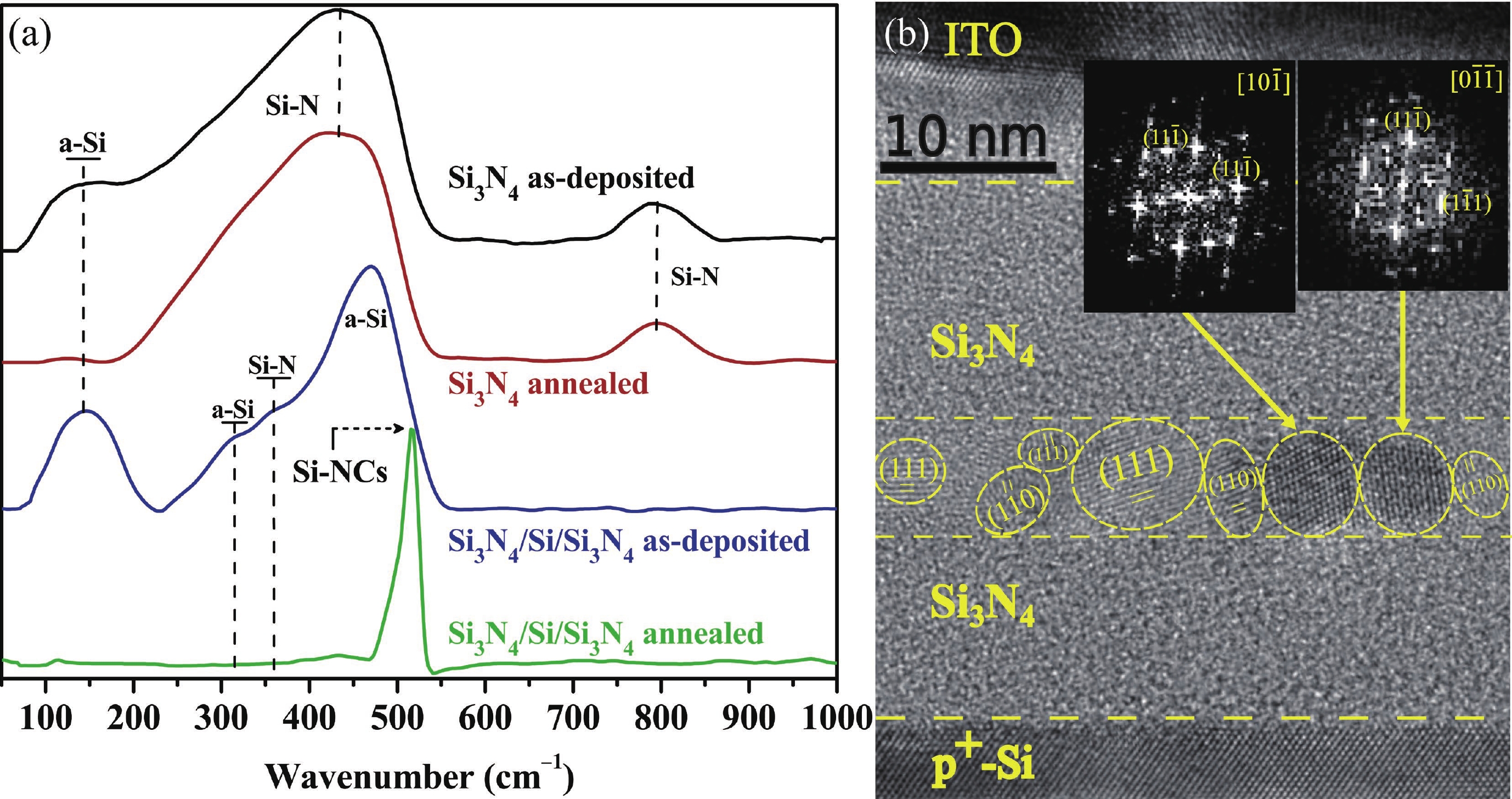
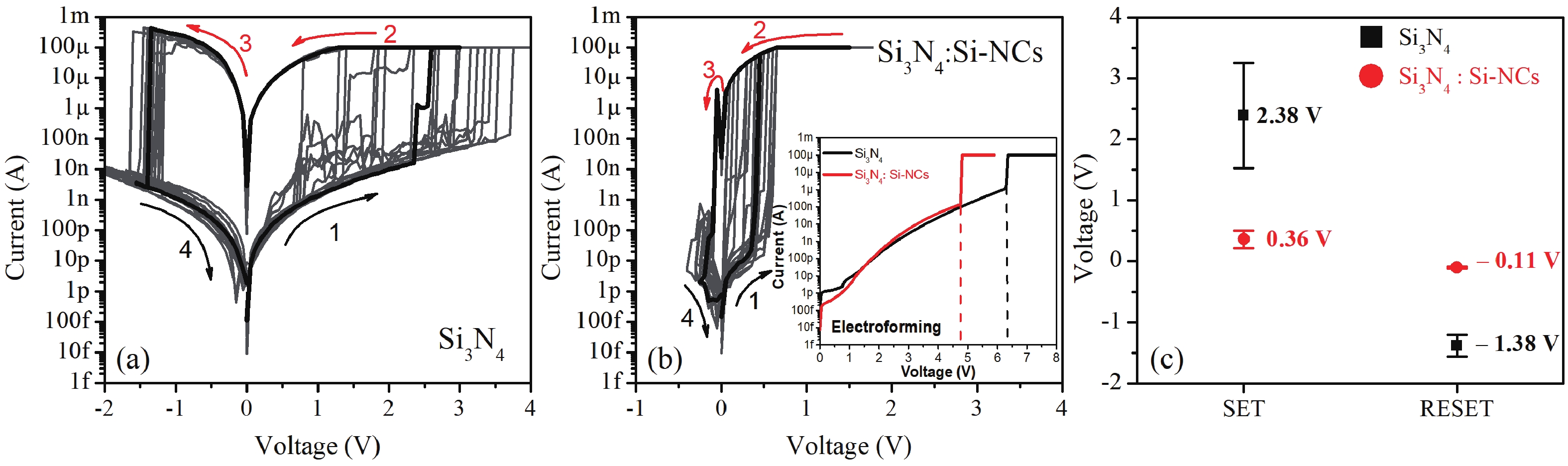
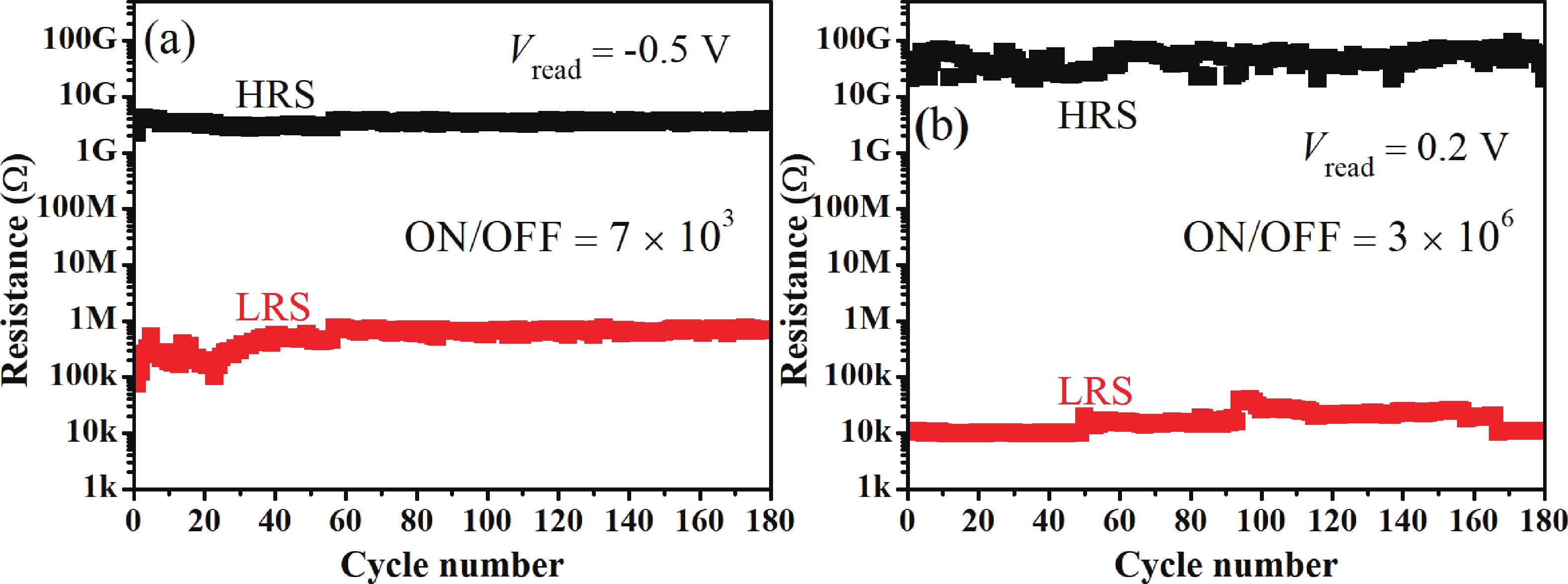
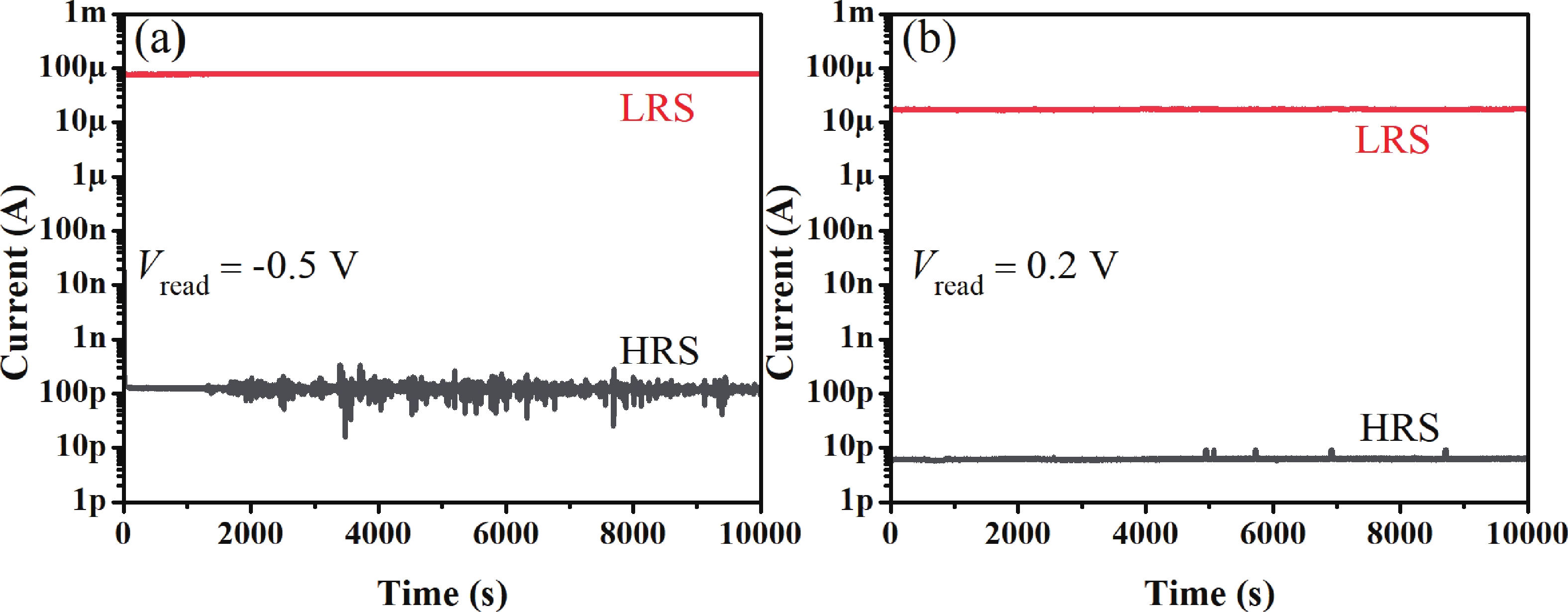
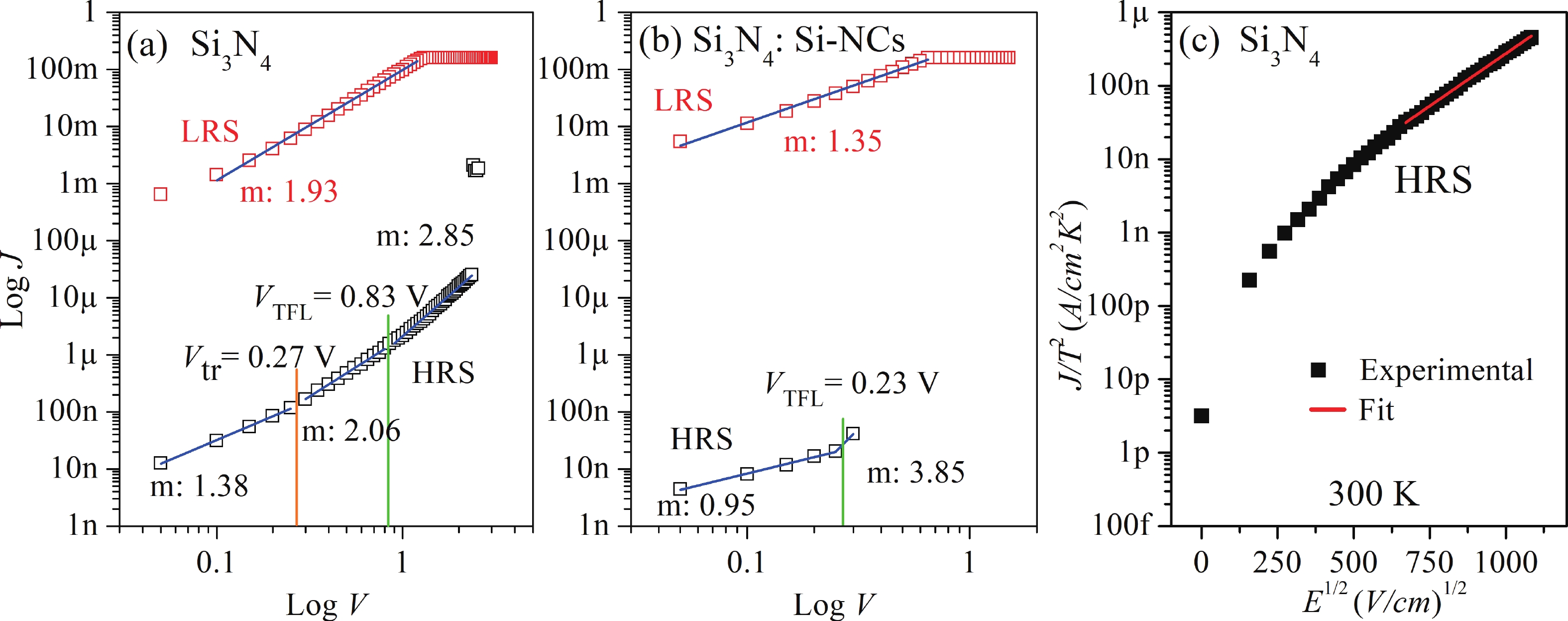
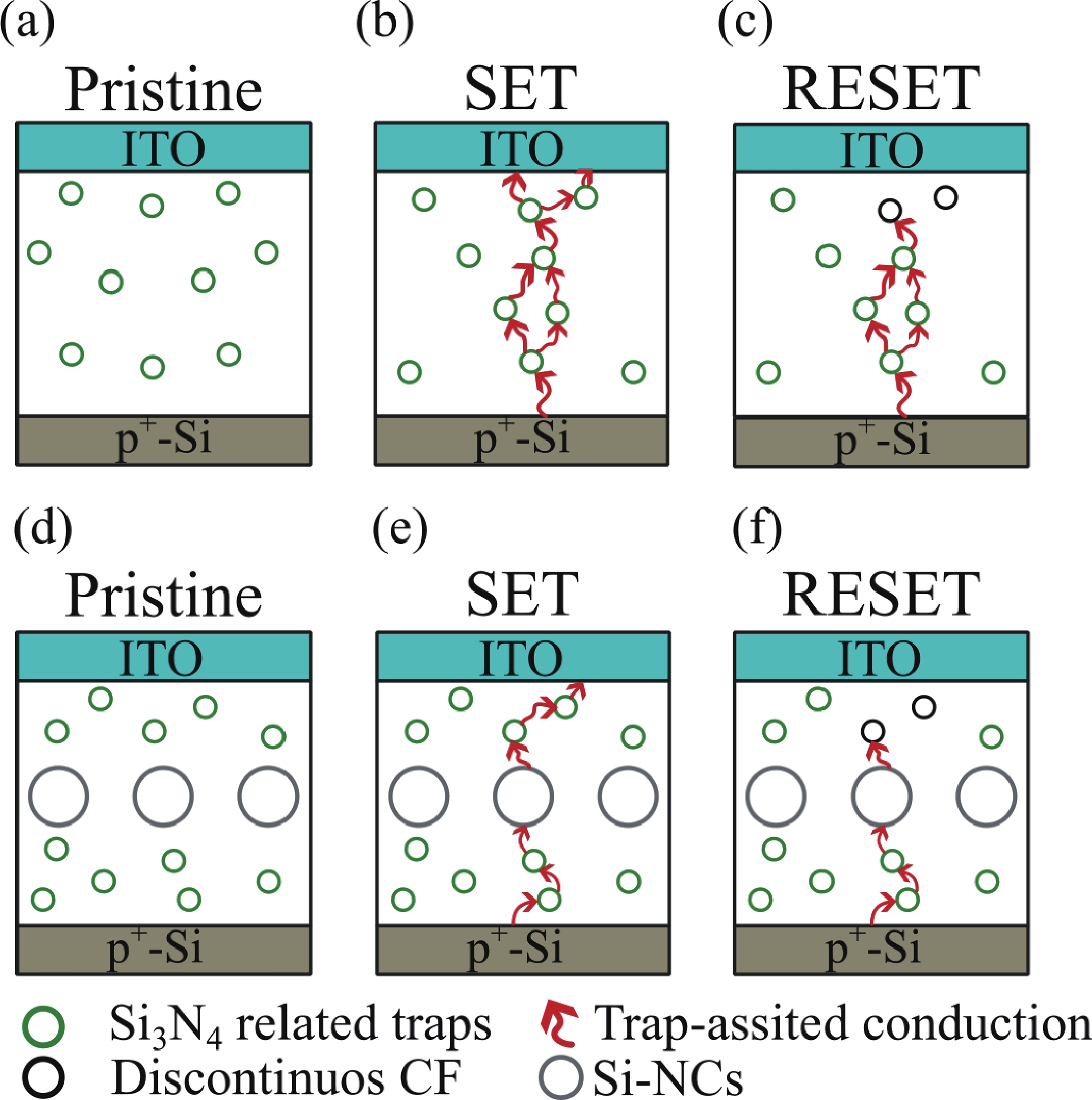
This work focuses on the study of the resistive switching (RS) properties of metal−insulator−semiconductor (MIS)-like structures based on silicon nitride (Si3N4) and Si3N4 with embedded silicon nanocrystals (Si-NCs) as the switching layer for the development of memristor devices. The formation of Si-NCs in the Si3N4 matrix, along with its chemical composition, was confirmed by Raman, transmission electron microscope (TEM), and energy-dispersive X-ray spectroscopy (EDS) analyses. The introduction of Si-NCs within the Si3N4 improved the performance of the devices. For Si3N4-based memristor devices, SET and RESET voltages of 2.38 and −1.38 V were obtained, respectively, while these values were reduced to 0.36 V (SET) and −0.11 V (RESET) for Si3N4:Si-NCs-based RS devices. Both RS devices exhibit at least 180 RS cycles, but with an increased ON/OFF ratio from 103 (Si3N4) to 106 when Si-NCs are embedded. The retention time analysis shows that the low resistance state (LRS) and the high resistance state (HRS) are stable for up to 104 s. The analysis of the conduction mechanism indicates that HRS is driven by the space-charge-limited conduction (SCLC), and the LRS by an Ohmic conduction mechanism. A model of the RS mechanism was proposed to understand the role of Si-NCs in the dielectric matrix.
J. Semicond.
2026, 47(4): 042306 doi: 10.1088/1674-4926/25100008
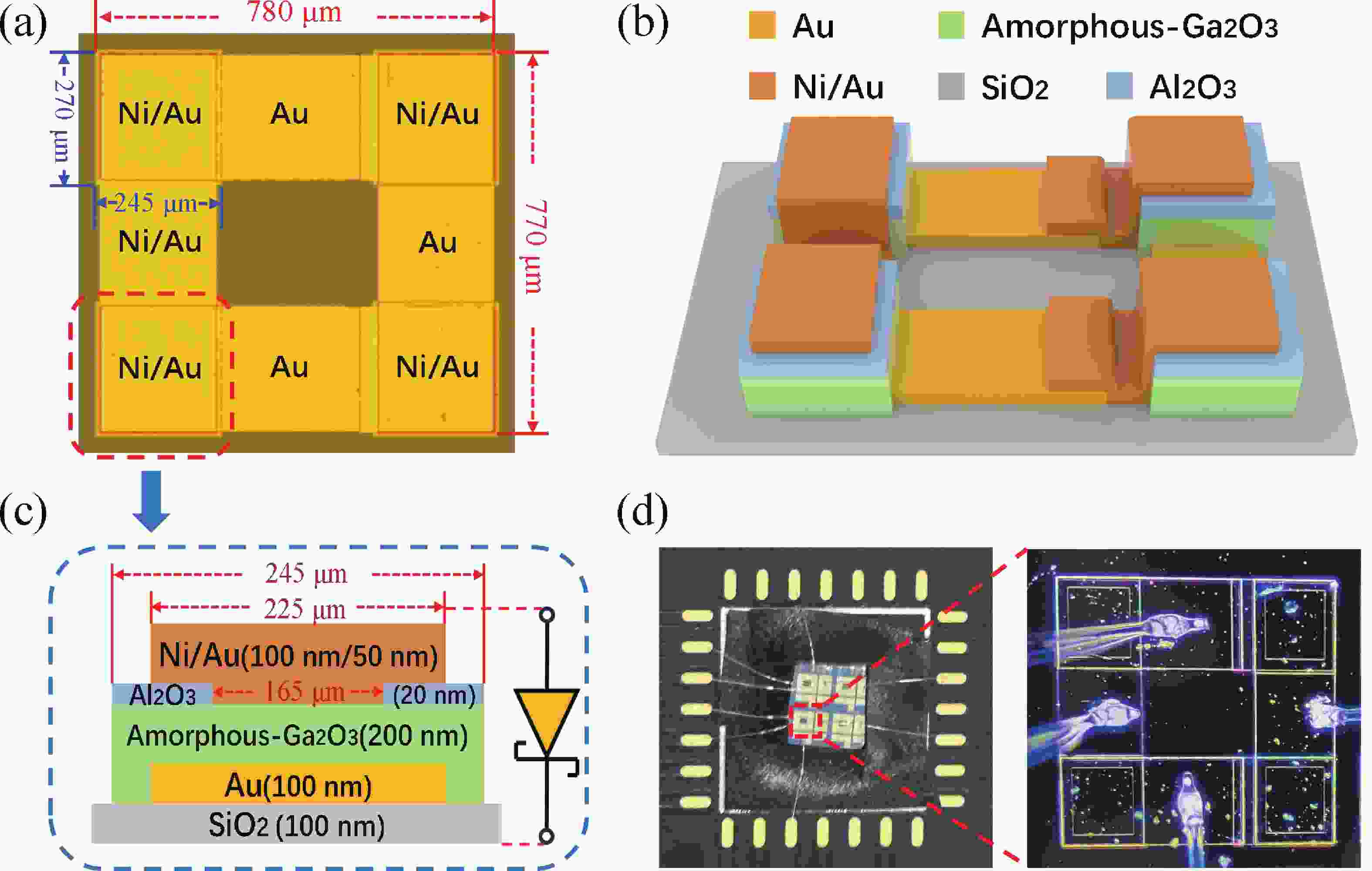
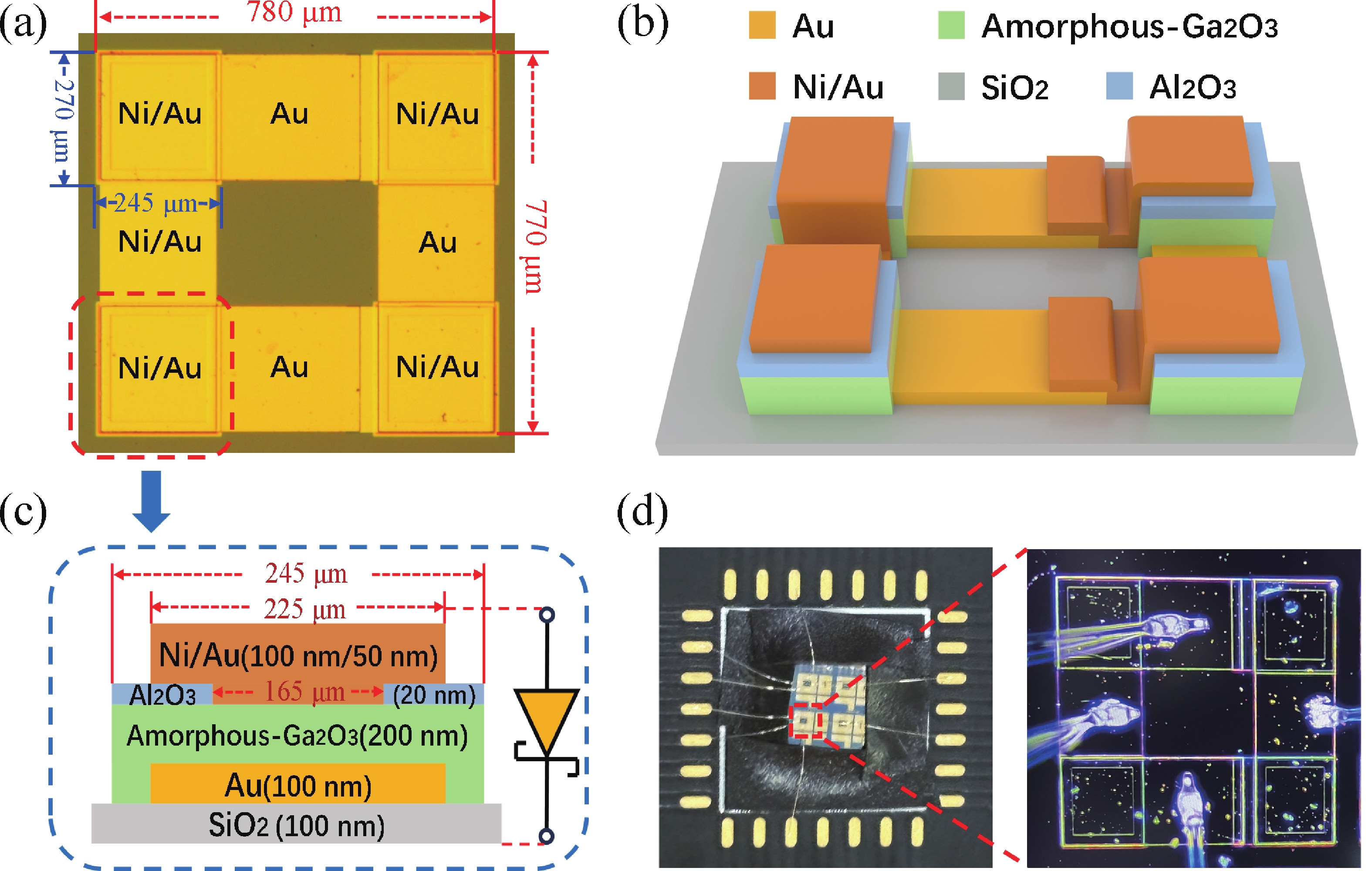
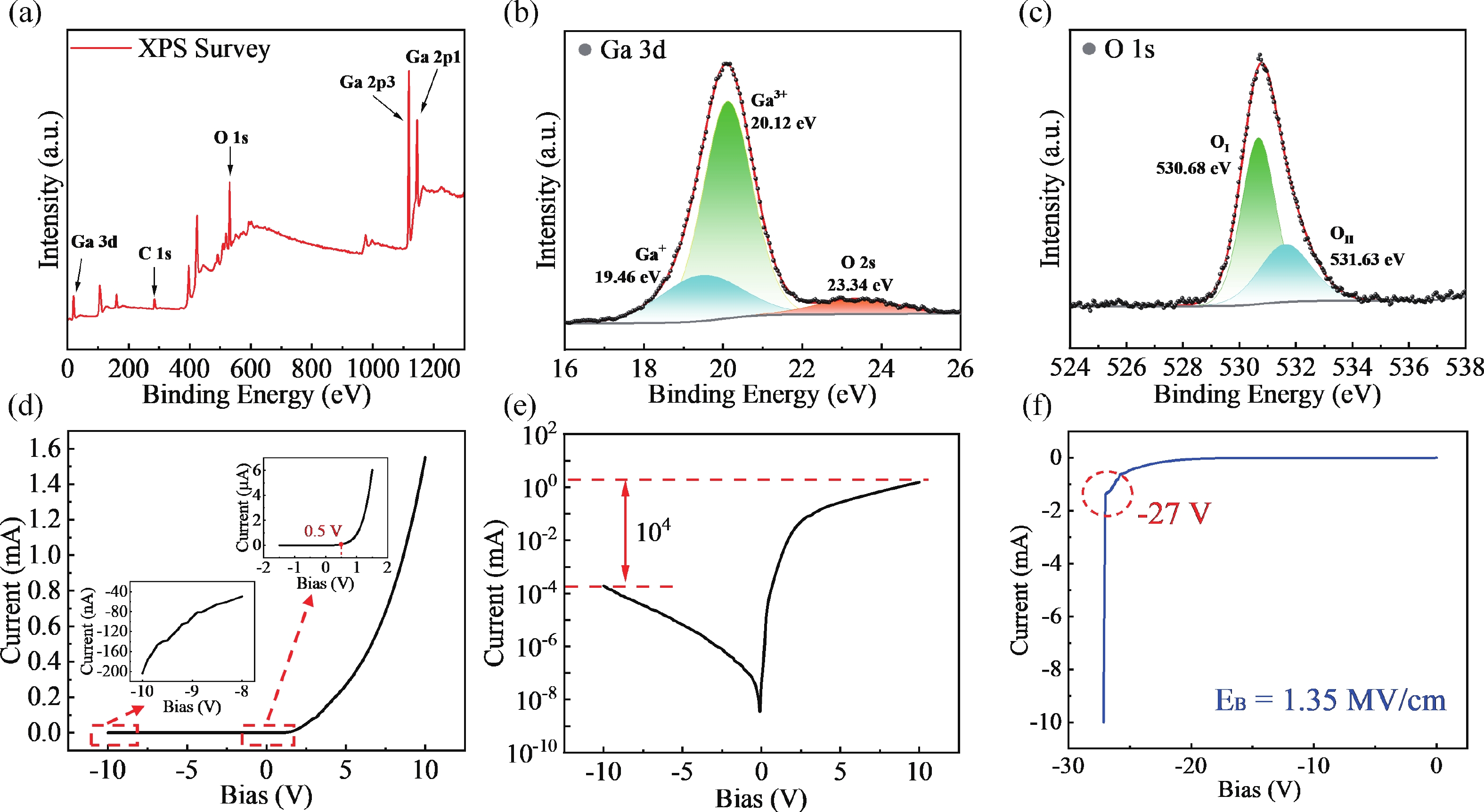
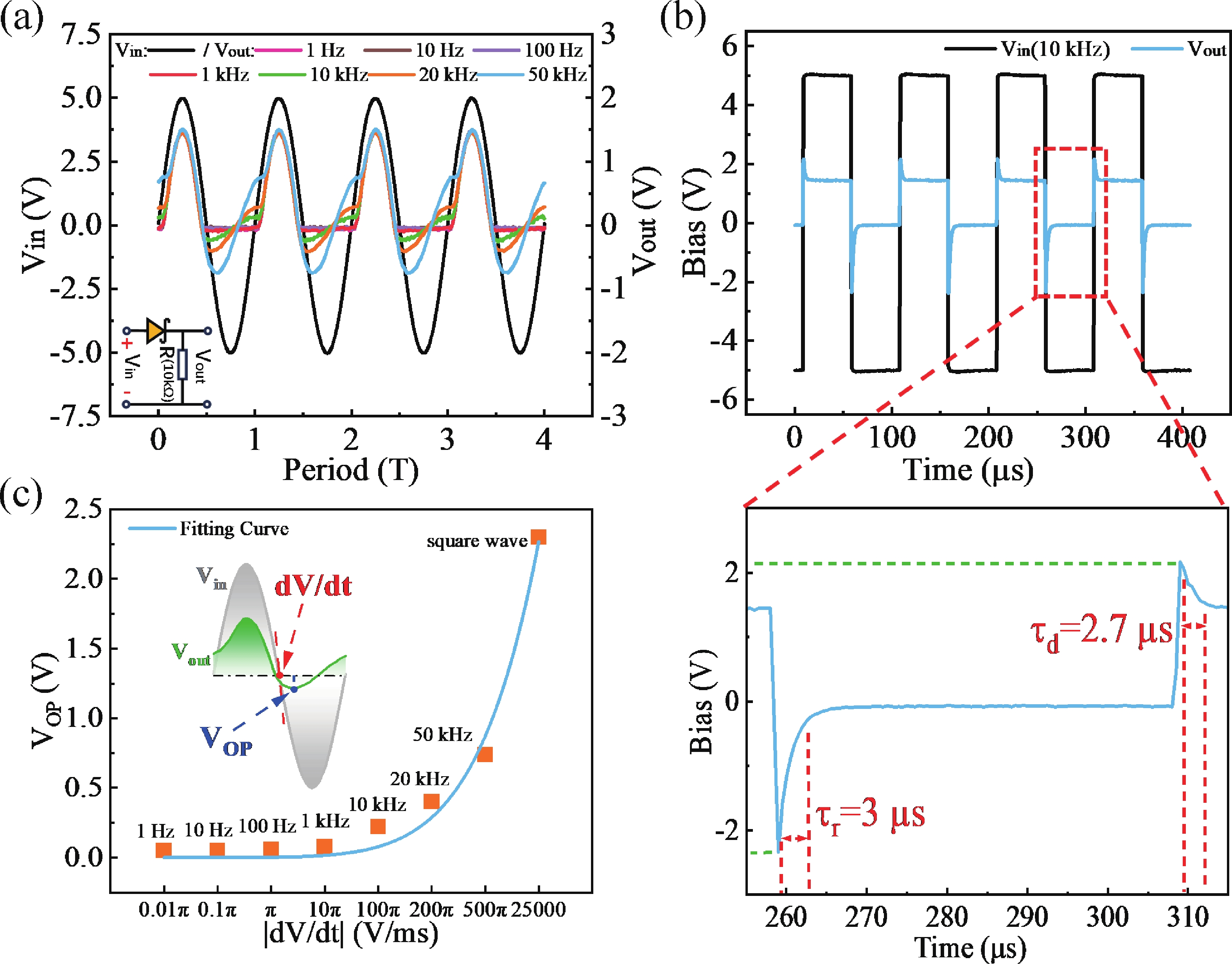
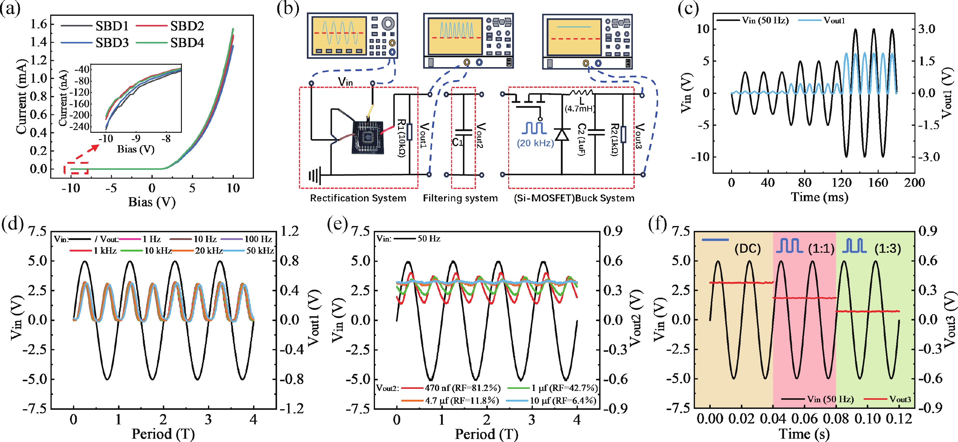
This paper demonstrated a monolithically integrated 200 nm-ultrathin amorphous-Ga2O3 vertical SBD-based bridge rectifier and its hybrid buck conversion system with a Si-MOSFET. The fabricated vertical Ga2O3 SBD exhibits excellent characteristics and a high breakdown electric field strength of 1.35 MV/cm. The bridge rectifier circuit maintains stable operation at high frequencies of 50 kHz. And the hybrid buck system composed of the Ga2O3 bridge rectifier and Si-MOSFET achieves adjustable step-down voltage output under the conditions of a 20 kHz switching frequency of Si-MOSFET and 50 Hz Vin. This work validates the practical value of Ga2O3 rectifiers in high-frequency conversion systems.
J. Semicond.
2026, 47(4): 042501 doi: 10.1088/1674-4926/25110026
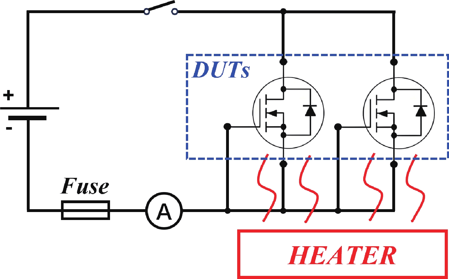
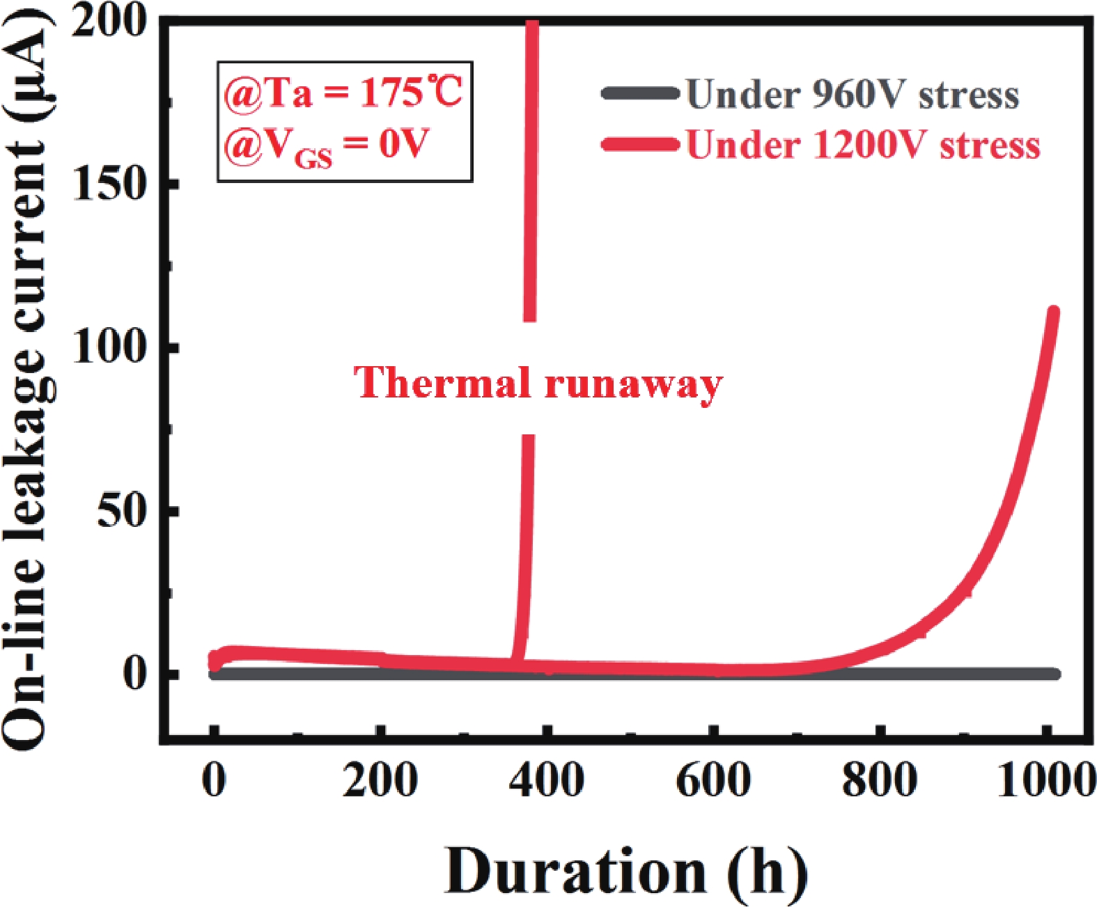
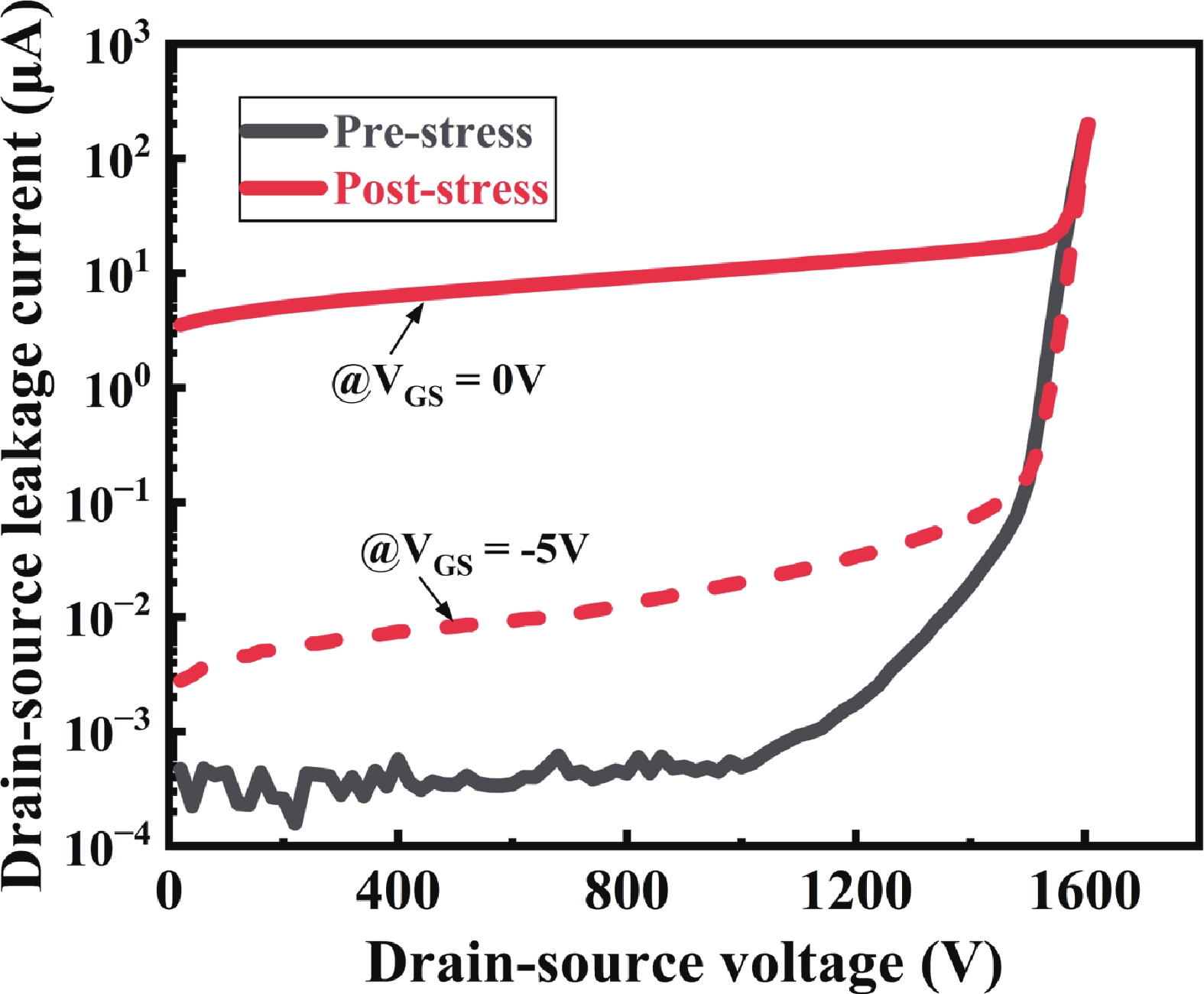
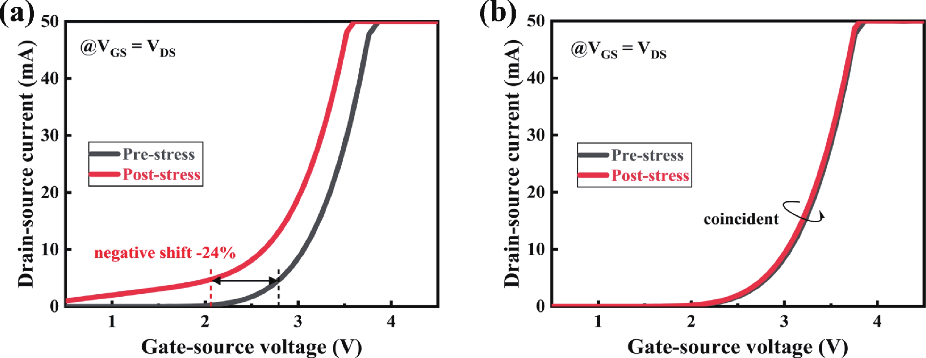
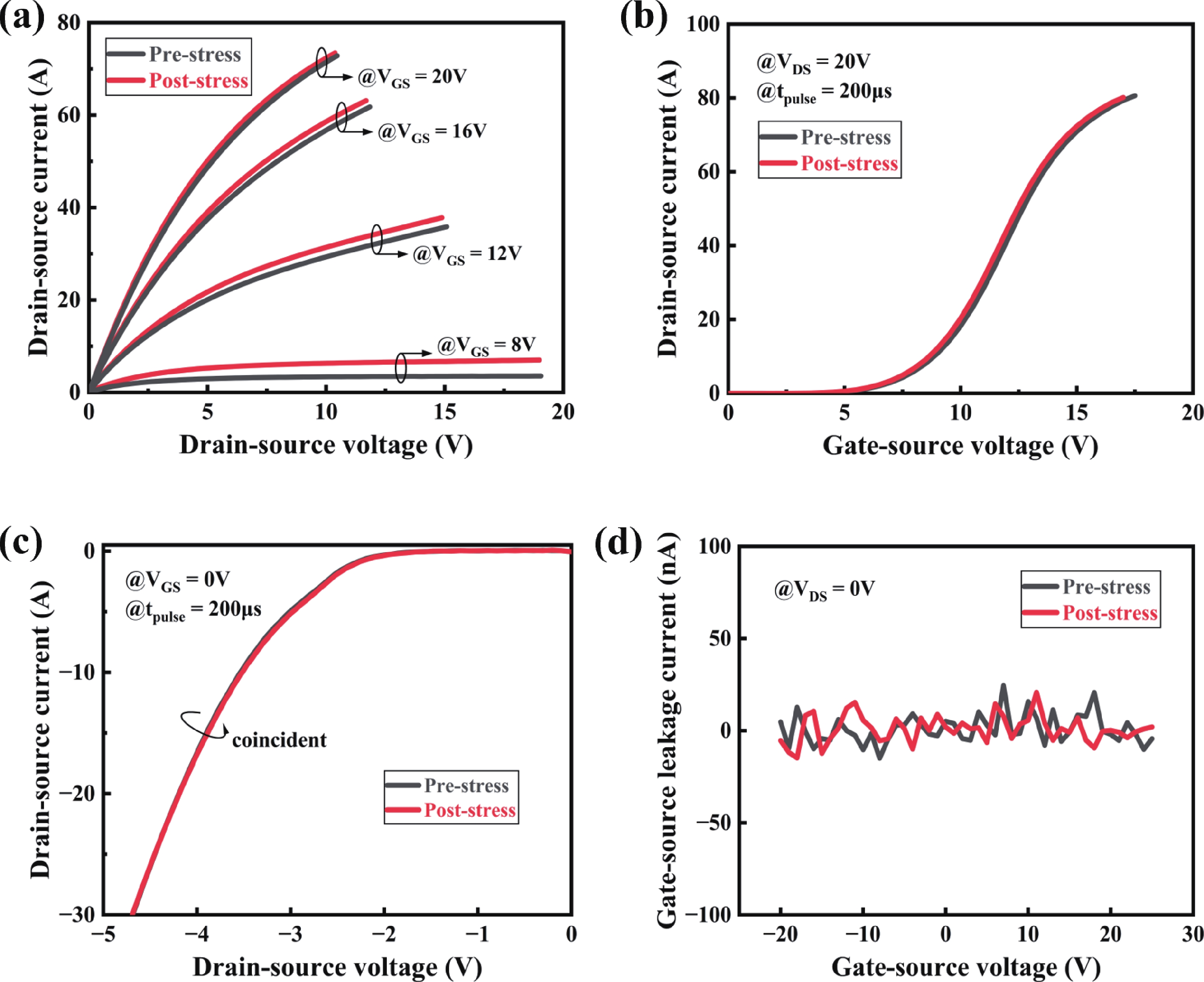
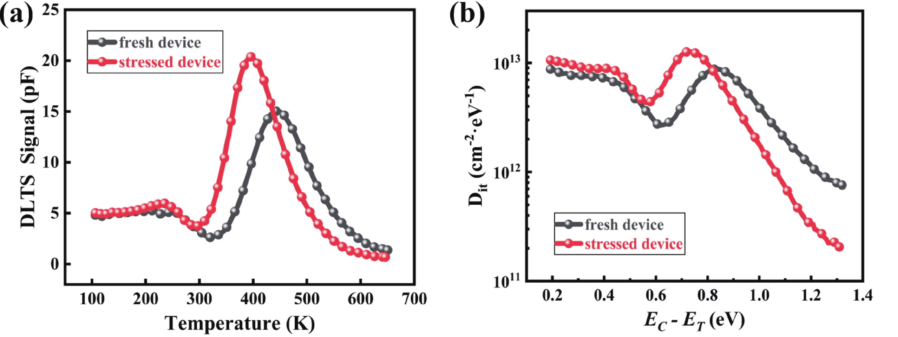
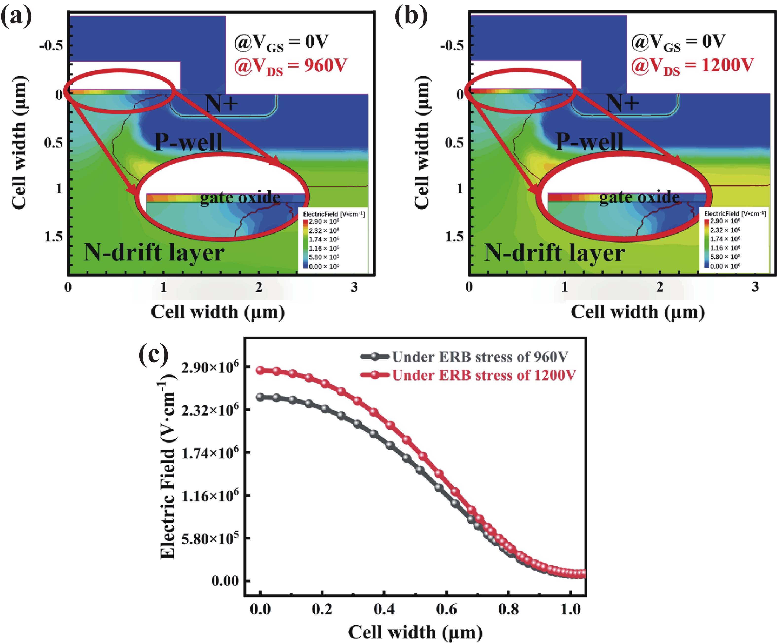
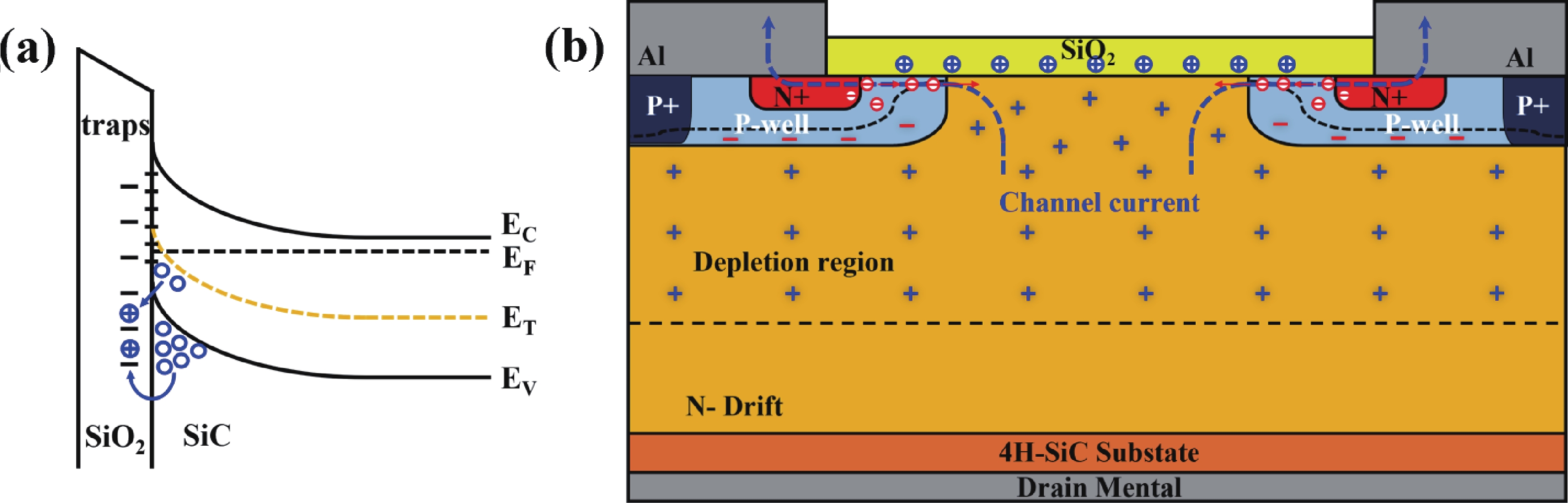
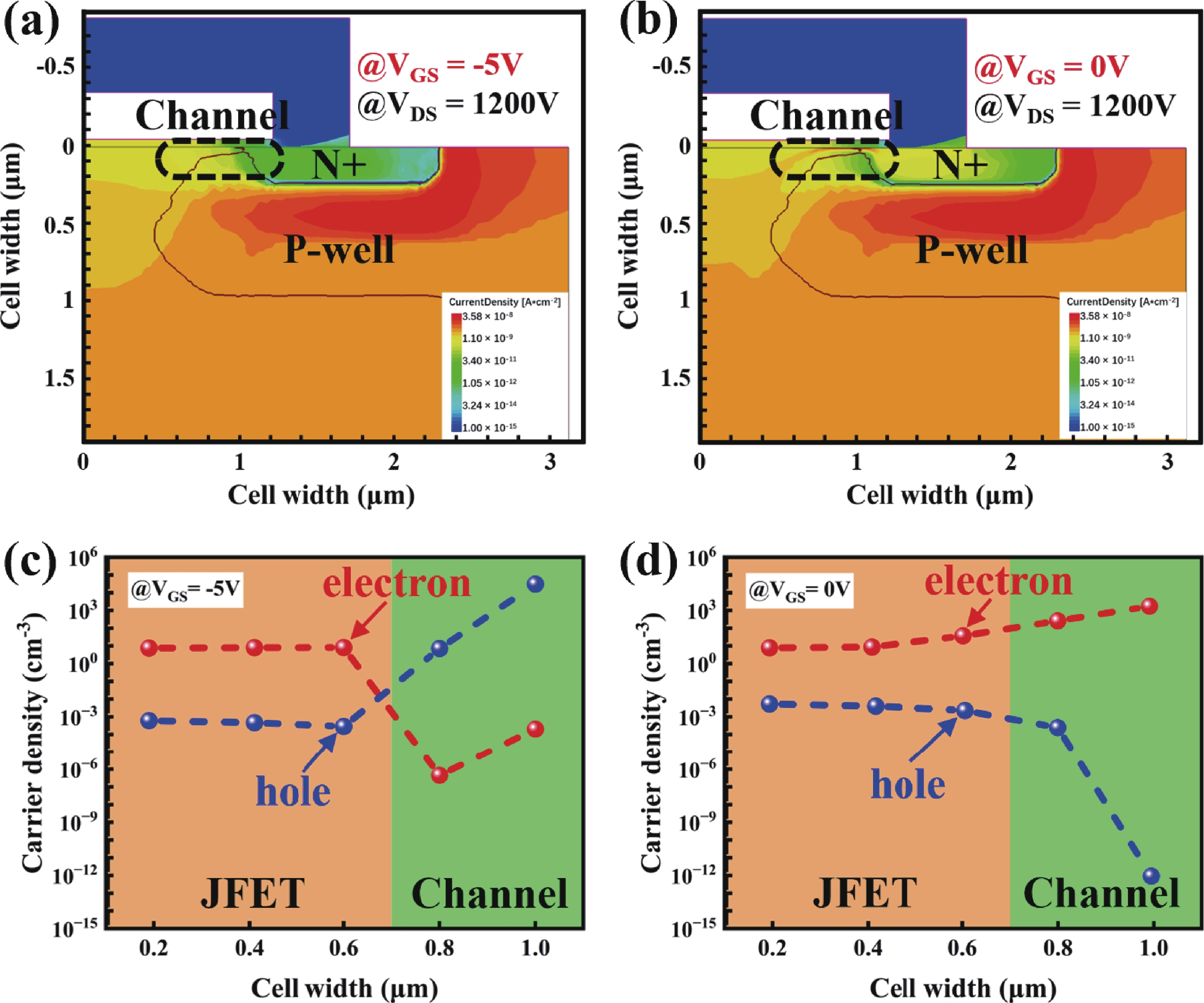
High-temperature reverse bias (HTRB) is one of the most critical reliability for SiC MOSFET, and the termination region is widely regarded as the sensitive area under HTRB stress. Interestingly, through systematically monitoring of the degradation behavior of static electrical parameters under different voltage, this study reveals that the elevated reverse bias (ERB) stress can also induce damage in the gate oxide, which results in the hole trapping and a negative shift of the threshold voltage. Deep level transient spectroscopy (DLTS) measurements were performed and showed that the interface trap density in the gate oxide is promoted after ERB stress. Surprisingly, the reverse leakage current after ERB stress is significantly deteriorated at a gate bias of 0 V, while effectively suppressed by applying a negative gate bias (−5 V), which point to the synergistic effects of channel region on the breakdown voltage. Based on the gate oxide degradations and TCAD simulations, it is elucidated that the trapped positive interface charges in gate oxide cause band bending, leading to the formation of an electron accumulation layer in the channel region at 0 V gate bias and thus resulting in a dominant leakage path. This work reveals the impact and mechanism of the ERB stress induced gate oxide damage on the breakdown voltage and highlights the importance of gate oxide protection, which is of great significance for improving the reliability of SiC MOSFETs in elevated voltage applications.
J. Semicond.
2026, 47(4): 042801 doi: 10.1088/1674-4926/25120015

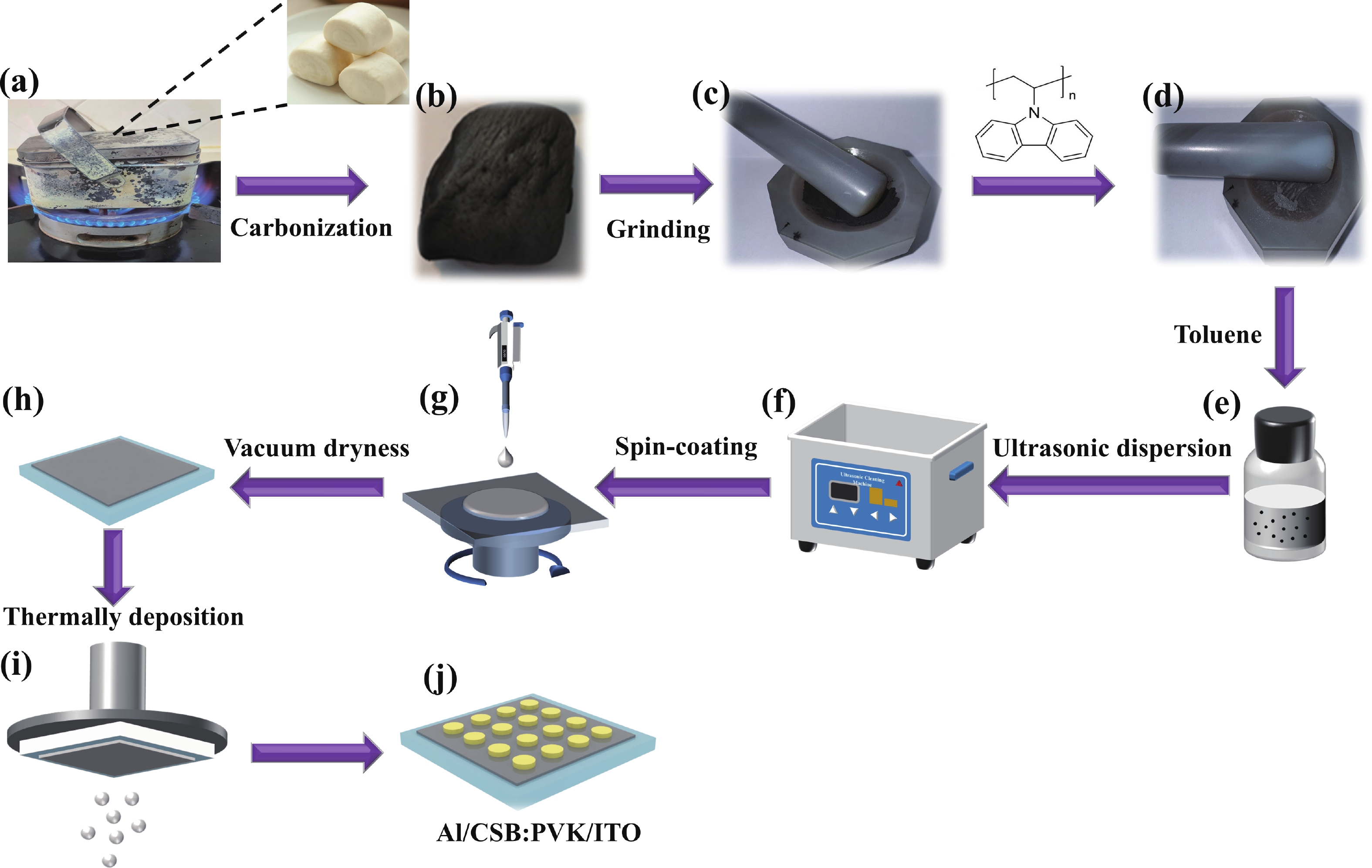
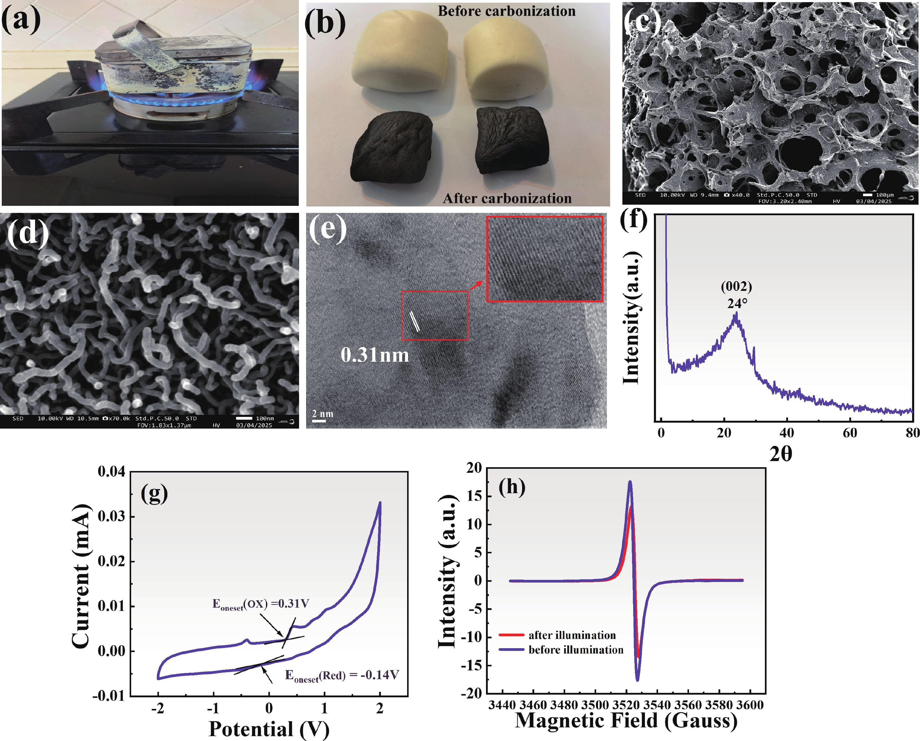
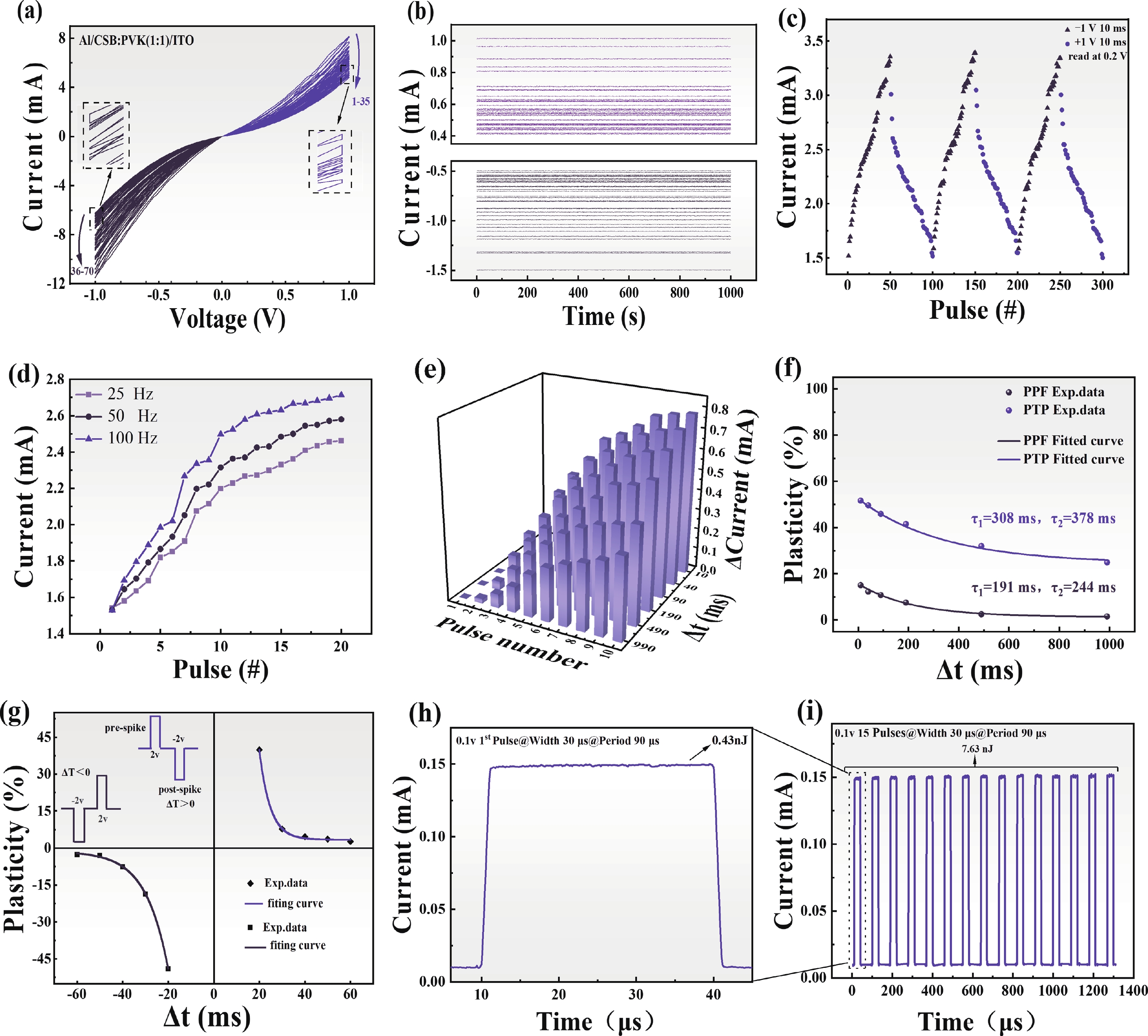
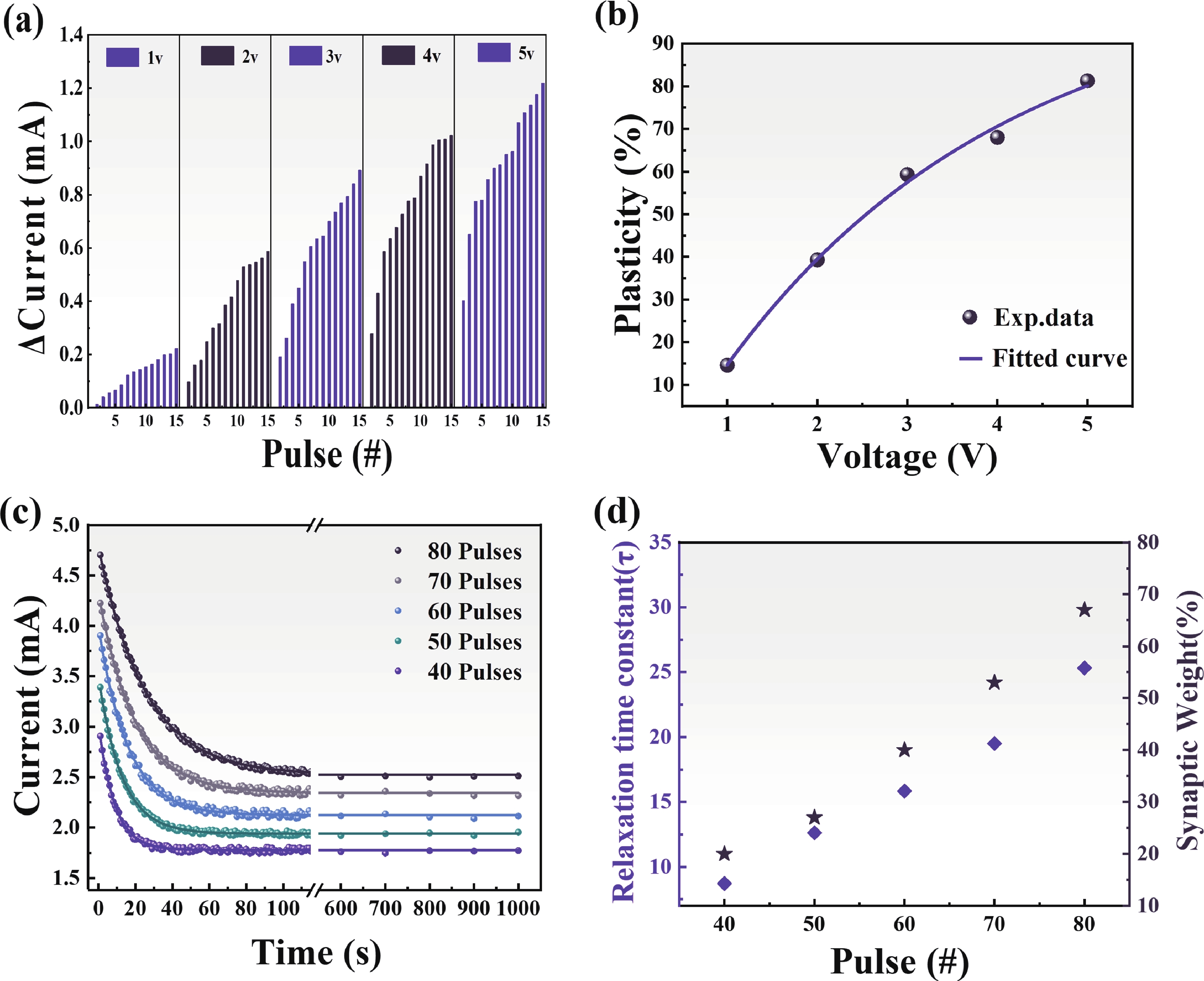
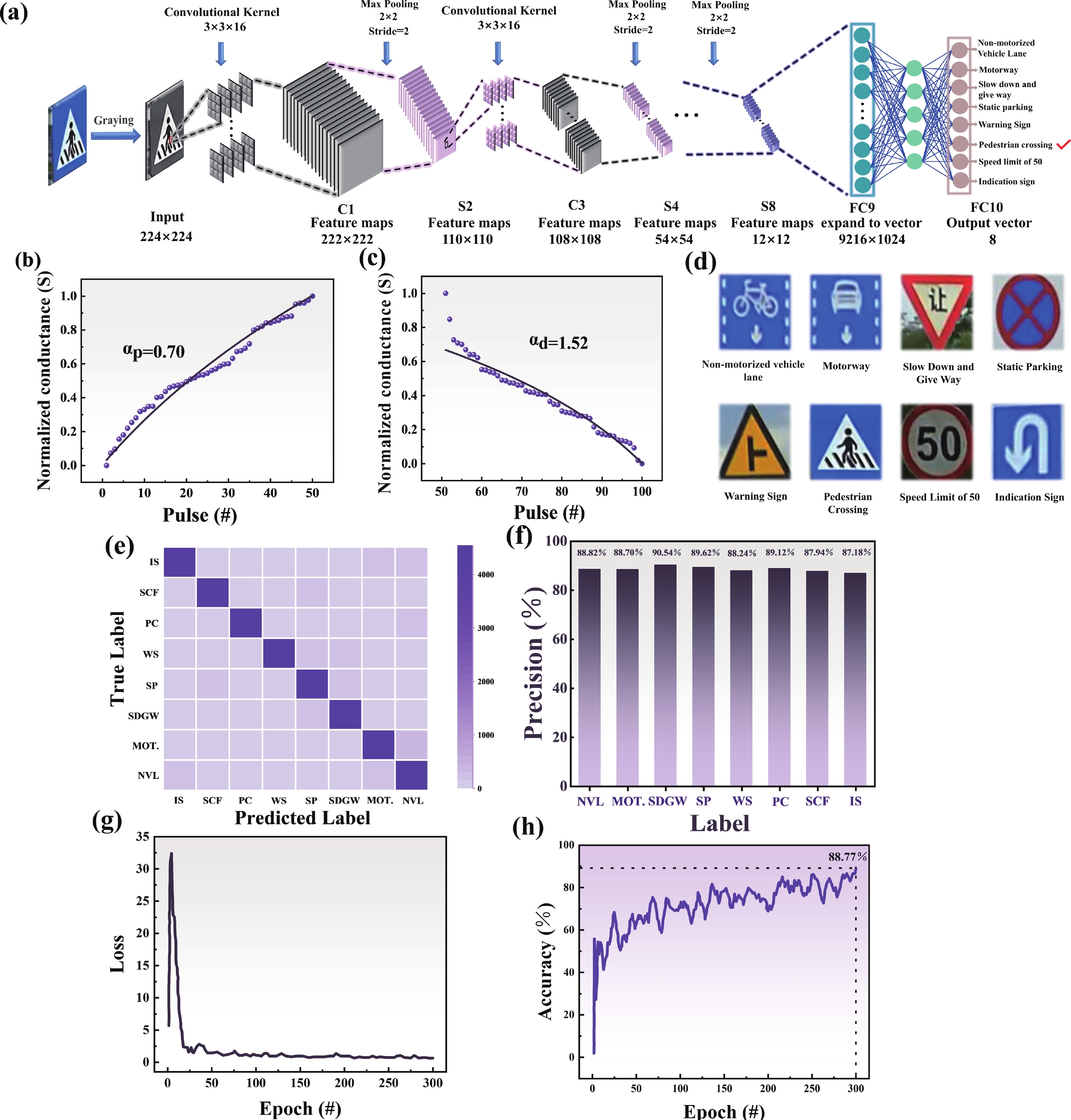
The development of new n-type semiconductors is crucial for the further advancement of electronic and optoelectronic devices. Steamed buns, anciently known as "man tou", mainly made of wheat flour and are one of the staple foods for Chinese people. After being subjected to high-temperature treatment, the steamed buns transformed into carbonized steamed buns (CSB) with porous nanostructures, which exhibit a Hall mobility of up to 1.62 cm2/(V·s), far greater than C60(1.5 × 10⁻³−2.5 × 10⁻² cm2/(V·s)), PCBM (2.0 × 10⁻⁷ cm2/(V·s)) and many polymer semiconductors (~10−6−10−2 cm2/(V·s)). A CSB-based bulk heterojunction memristor with a configuration of ITO/the CSB: PVK blends/Al is successfully fabricated. The device shows outstanding history dependent memristive switching performance, with 35 distinguishable conductance states, at a small sweep voltage range of ±1 V. An achieved production yield reaches up to 89%. Upon being subjected to consecutive positive or negative voltage sweeps, the current flowing through the device can be modulated continuously. When the 15 consecutive pulse voltages (pulse amplitude: 0.1 V; pulse width:10 μs, pulse period: 20 μs) were applied to the device, the observed total power consumption was about 7.63 nJ, suggesting a potential in low-energy neuromorphic computing applications. As expected, both the CSB and PVK do not exhibit any memristive effect under the same experimental condition. Utilizing the characteristic that the device can linearly adjust the weights, a simple convolutional neural network for traffic sign recognition was successfully constructed. After 300 rounds of training, the achieved recognition accuracy rate reached 88.77%. This work not only provides a new approach for developing low-cost and readily available organic semiconductors with high Hall mobility, but also offers a new idea for the subsequent development of high-performance artificial synapses and optoelectronic devices using carbonized steamed buns.
J. Semicond.
2026, 47(4): 042802 doi: 10.1088/1674-4926/25110031
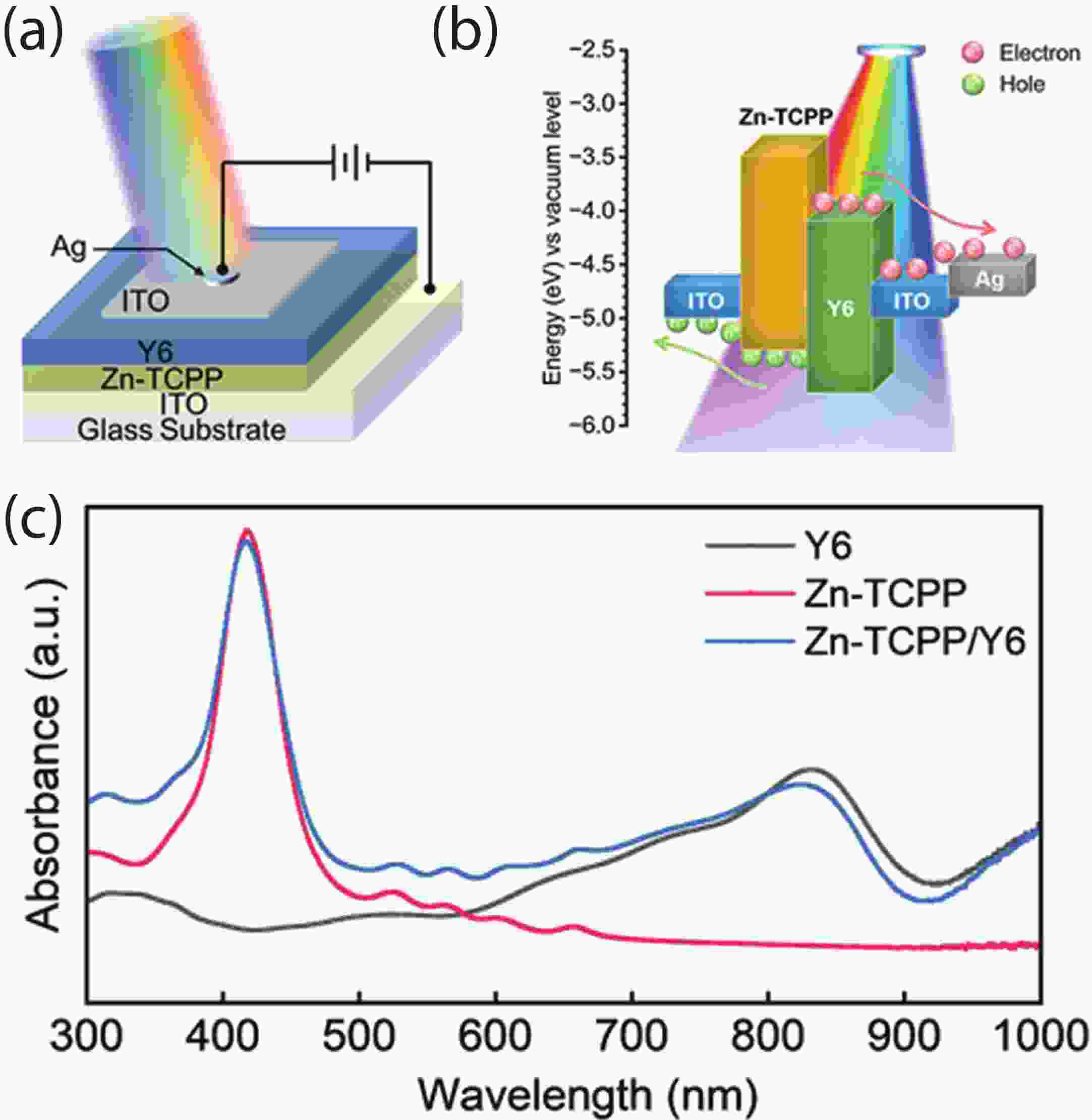
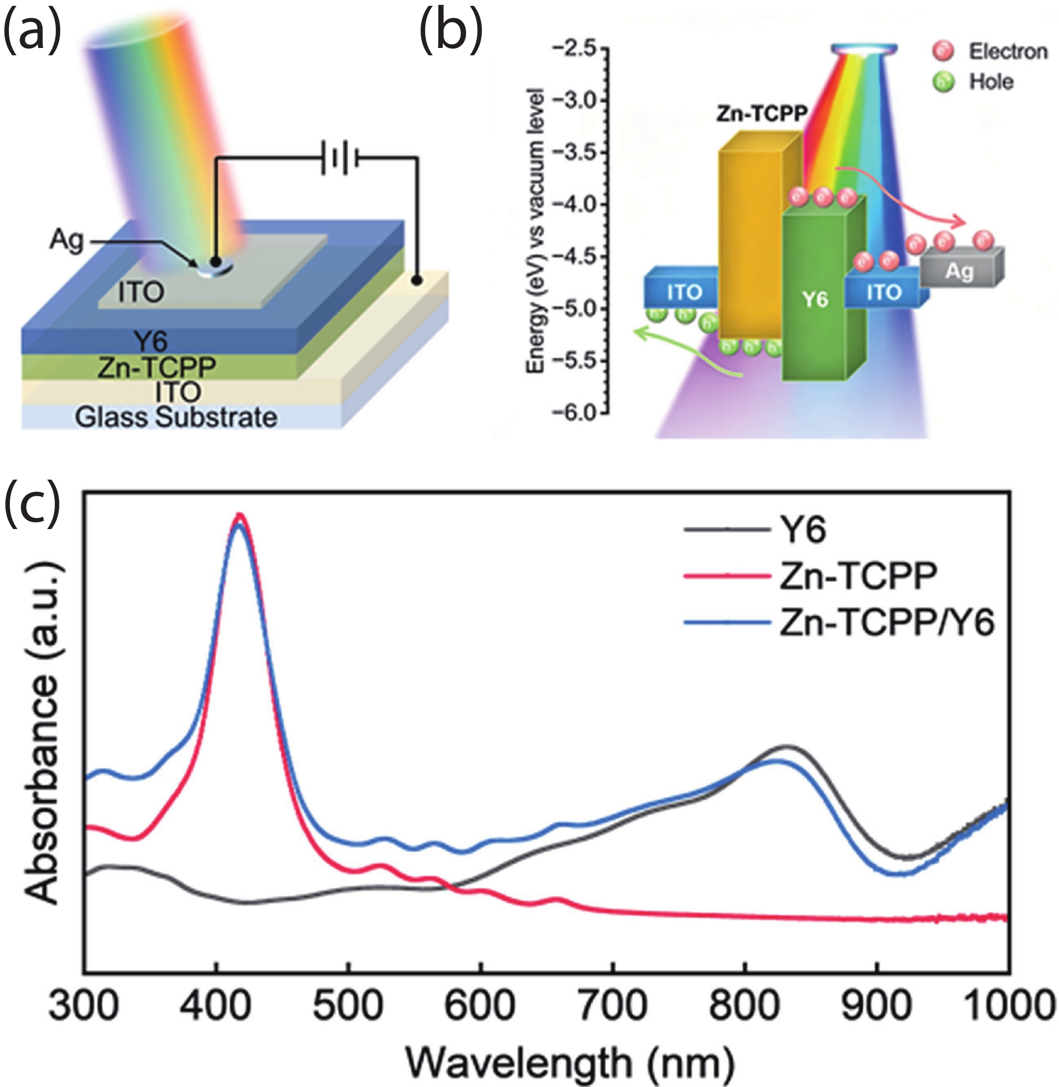
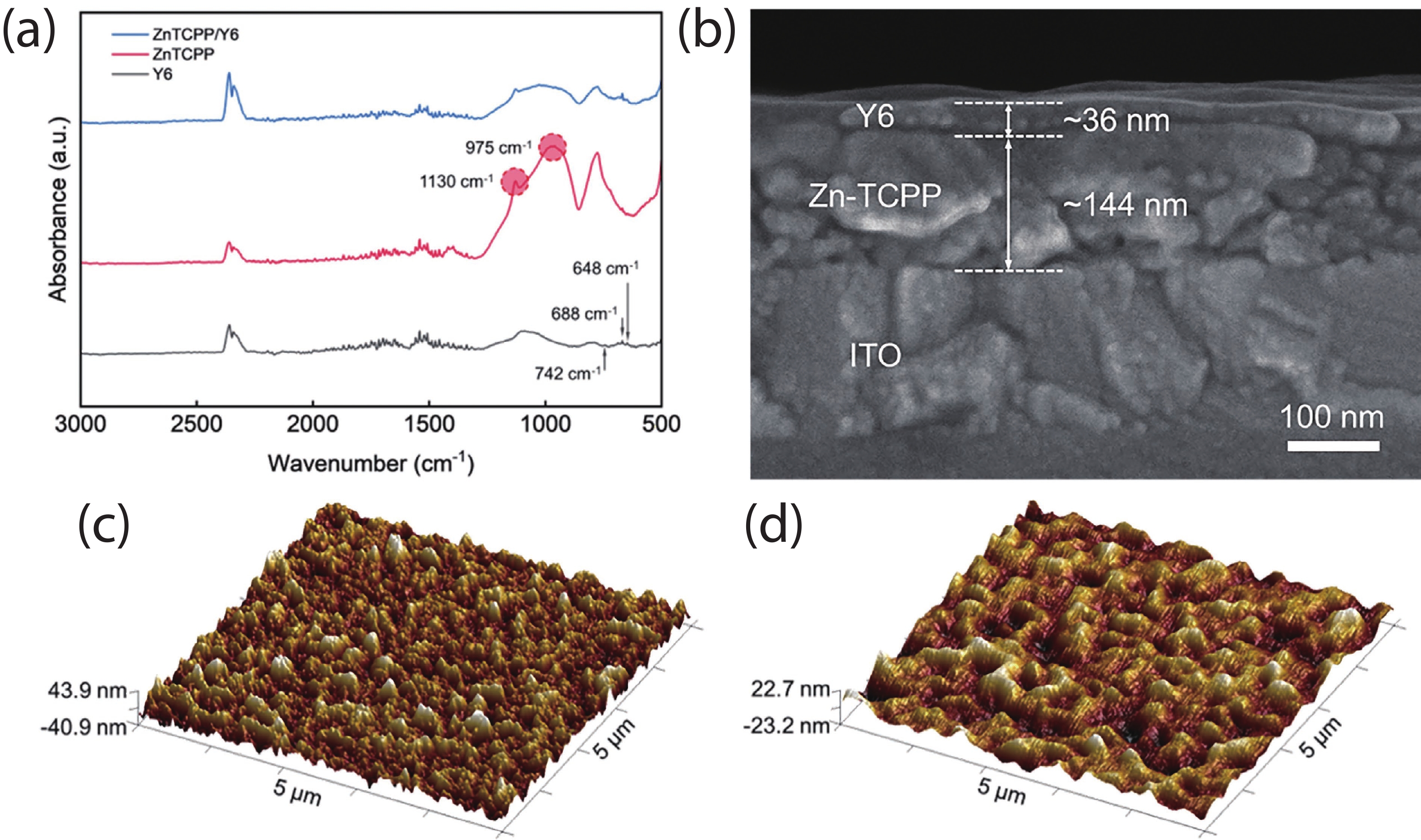
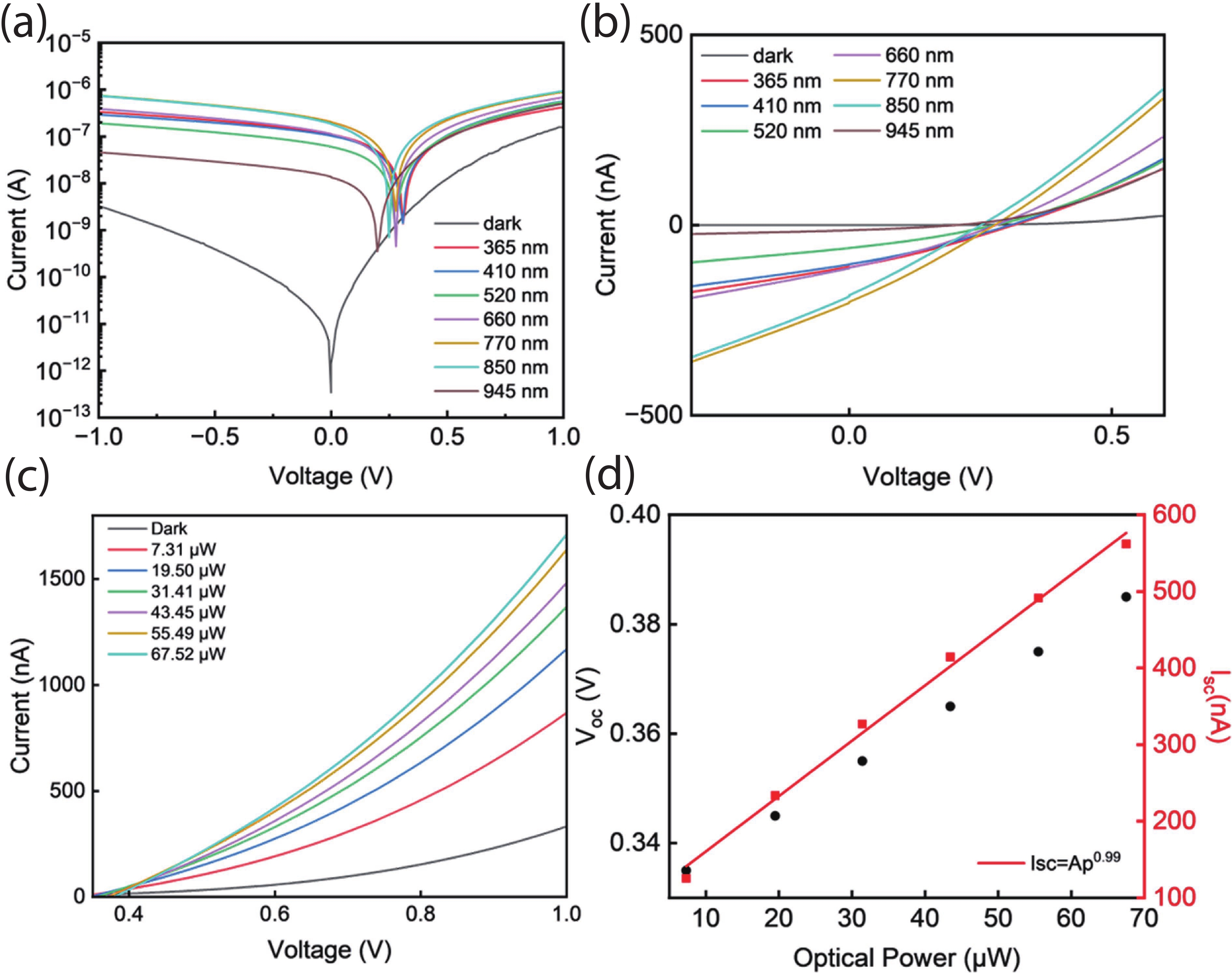
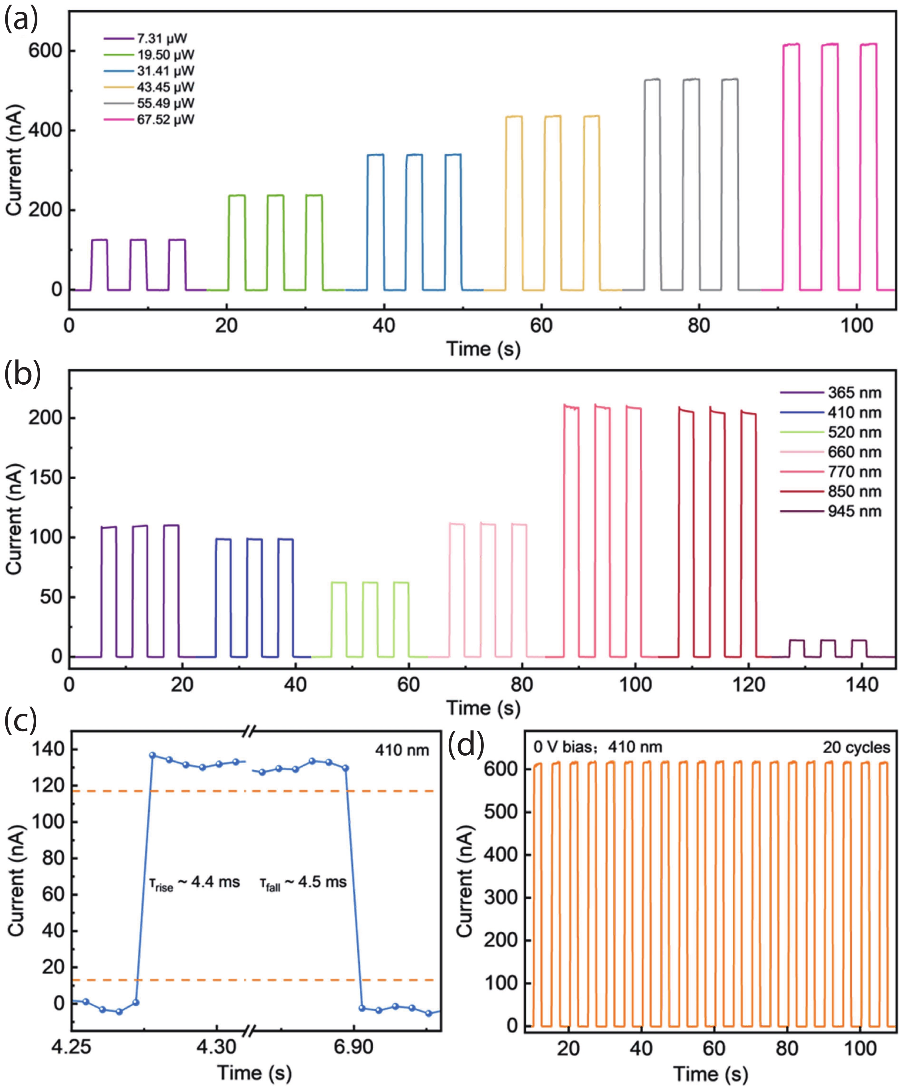
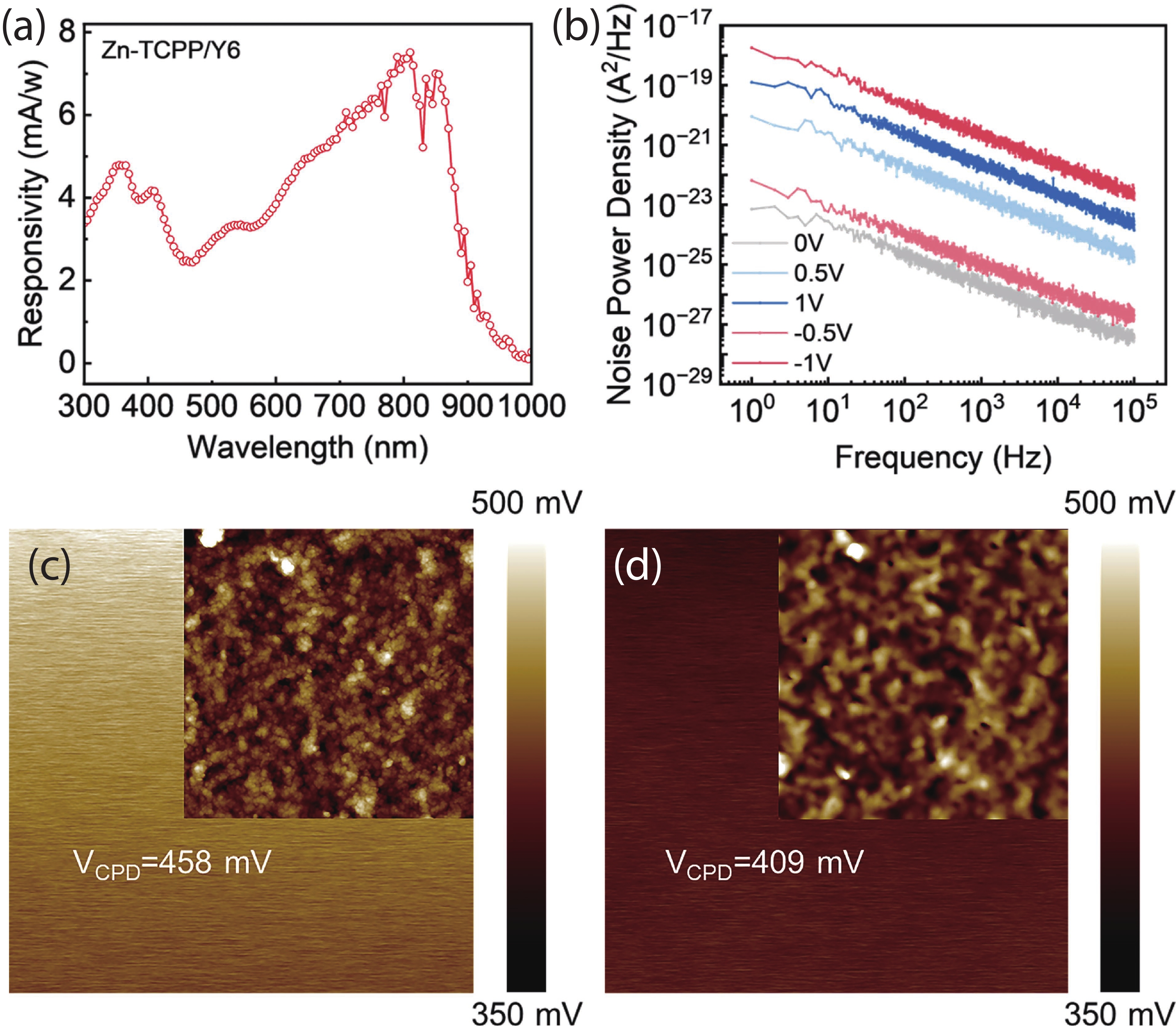
Broadband, low-power, and solution-processable organic photodetectors are essential for next-generation optoelectronic sensing. Two-dimensional conductive metal−organic frameworks (2D cMOFs) based on zinc tetracarboxyphenyl porphyrin (Zn-TCPP) offer strong light absorption and efficient charge transport, yet their photoresponse remains confined to the ultraviolet−visible (UV−Vis) region. To address this limitation, this study develops a solution-compatible strategy for constructing a well-defined MOF/organic semiconductor type-Ⅱ heterojunction by spin-coating a high-performance Y6 layer onto Zn-TCPP films. The resulting heterostructure provides complementary spectral absorption, promotes efficient exciton dissociation, and enables directional charge carrier transport, thereby achieving self-powered broadband photodetection spanning the ultraviolet to near-infrared (UV−NIR) range. The device demonstrates outstanding performance, including an ultra-low dark current (down to 3.40 × 10⁻¹³ A), high responsivity, and an ultrafast transient response with a rise time of 4.4 ms. This work establishes a generalizable approach for engineering high-efficiency MOF/organic semiconductor heterojunctions and offers a promising platform for low-cost, broadband, and self-powered photodetectors for biomedical and advanced sensing applications.