Issue Browser
Volume 47, Issue 3,
Mar 2026
Column
J. Semicond.
2026, 47(3): 031301 doi: 10.1088/1674-4926/25060031

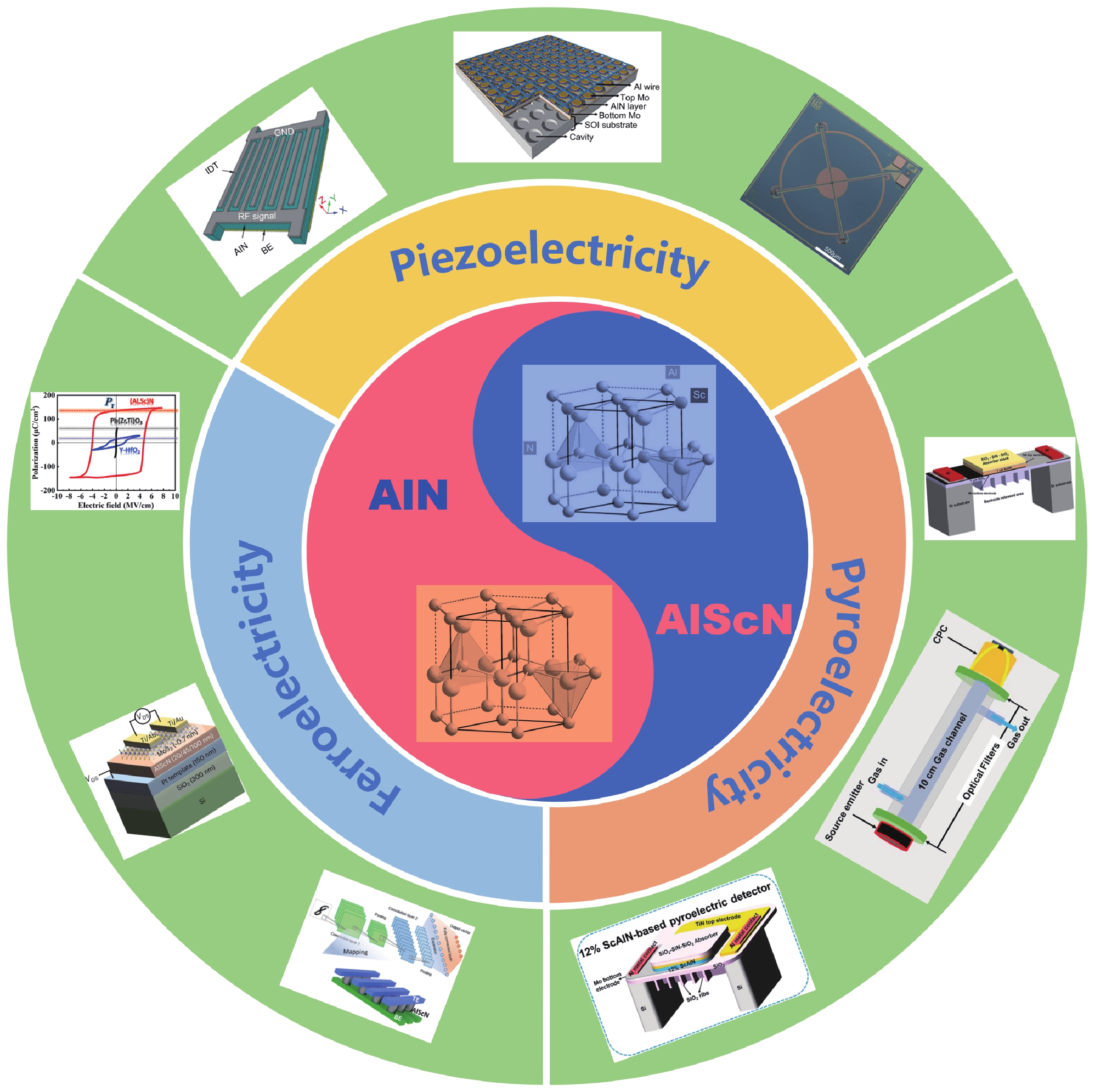
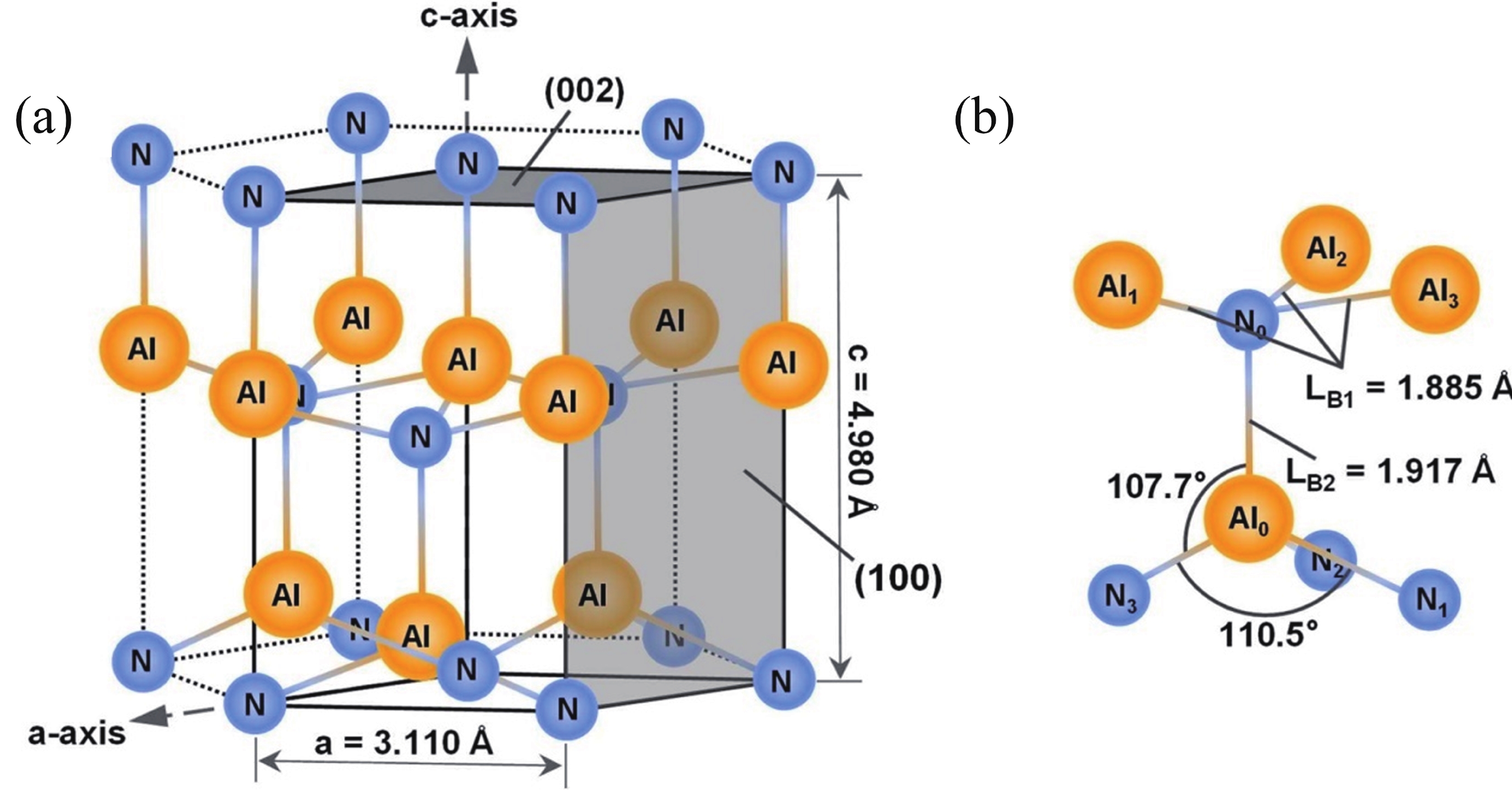
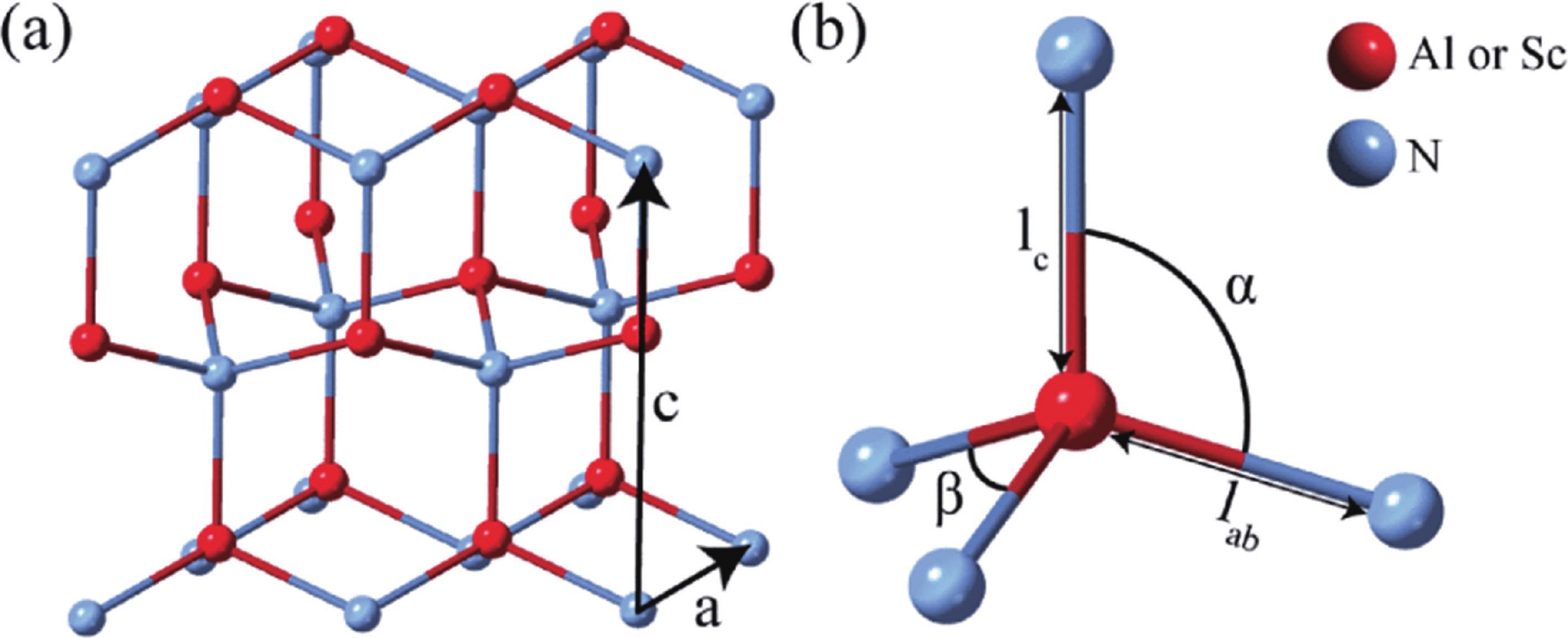
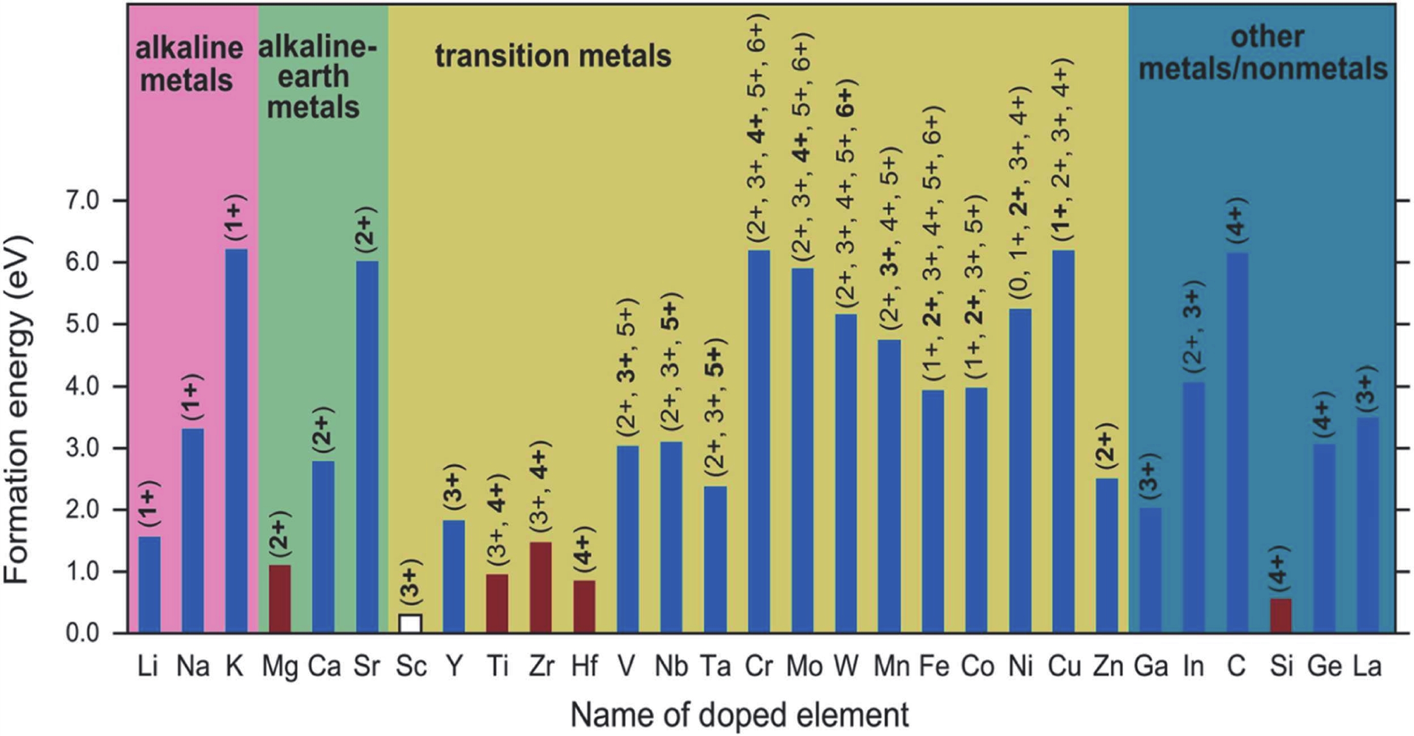
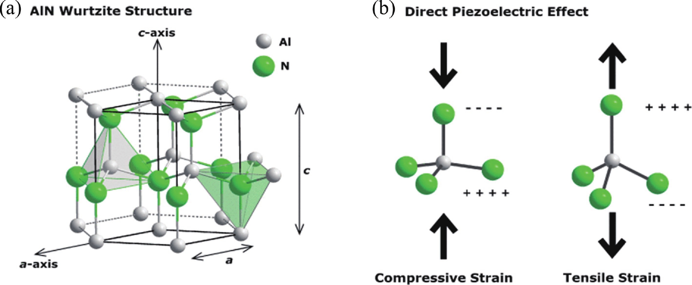
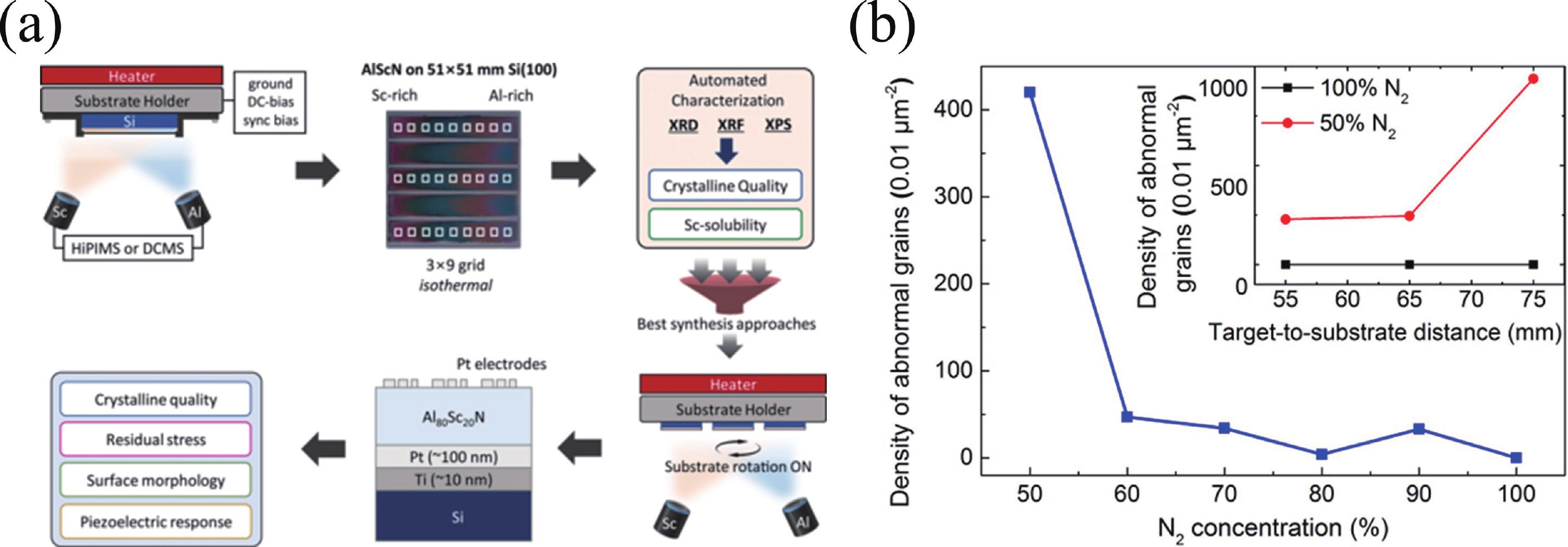
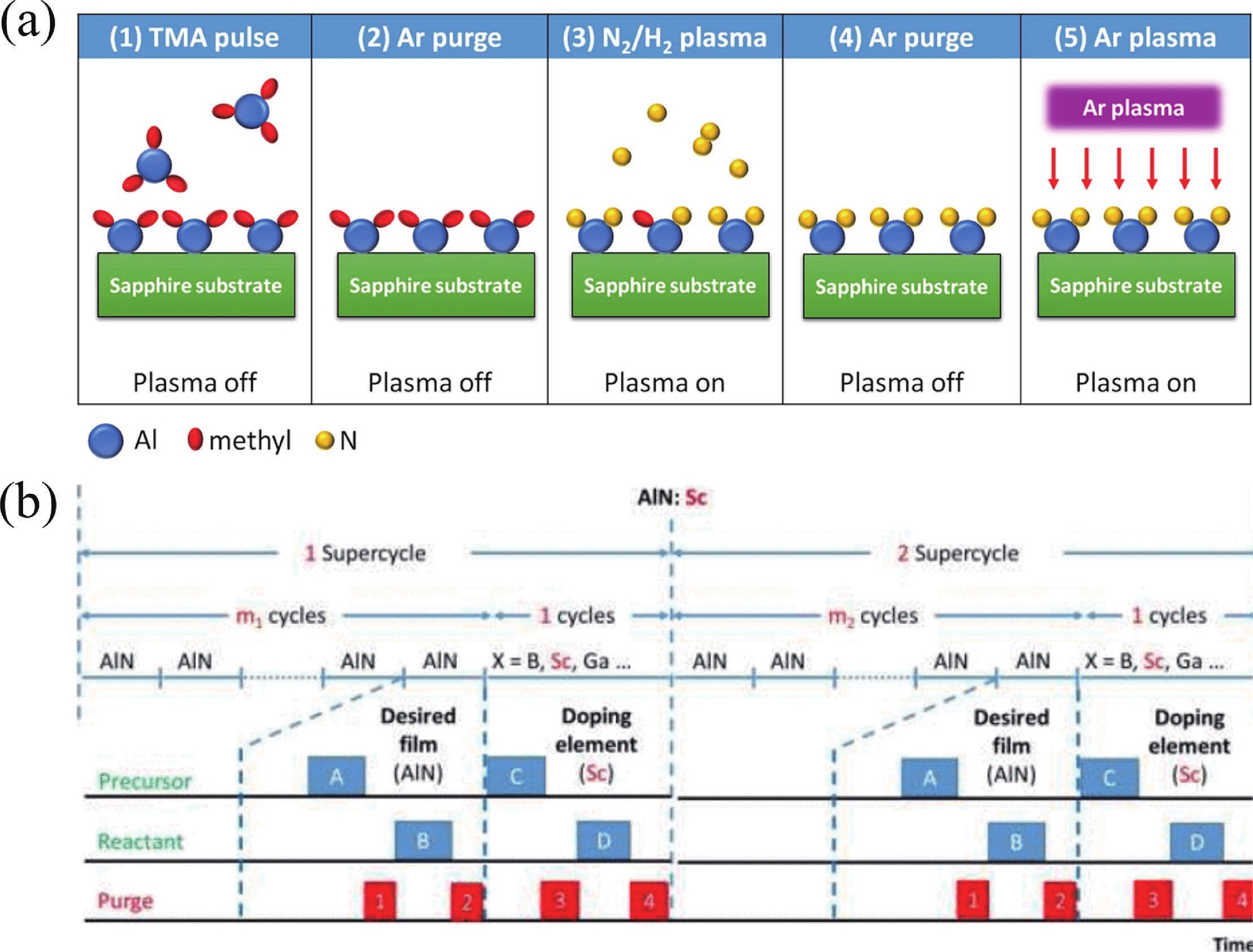
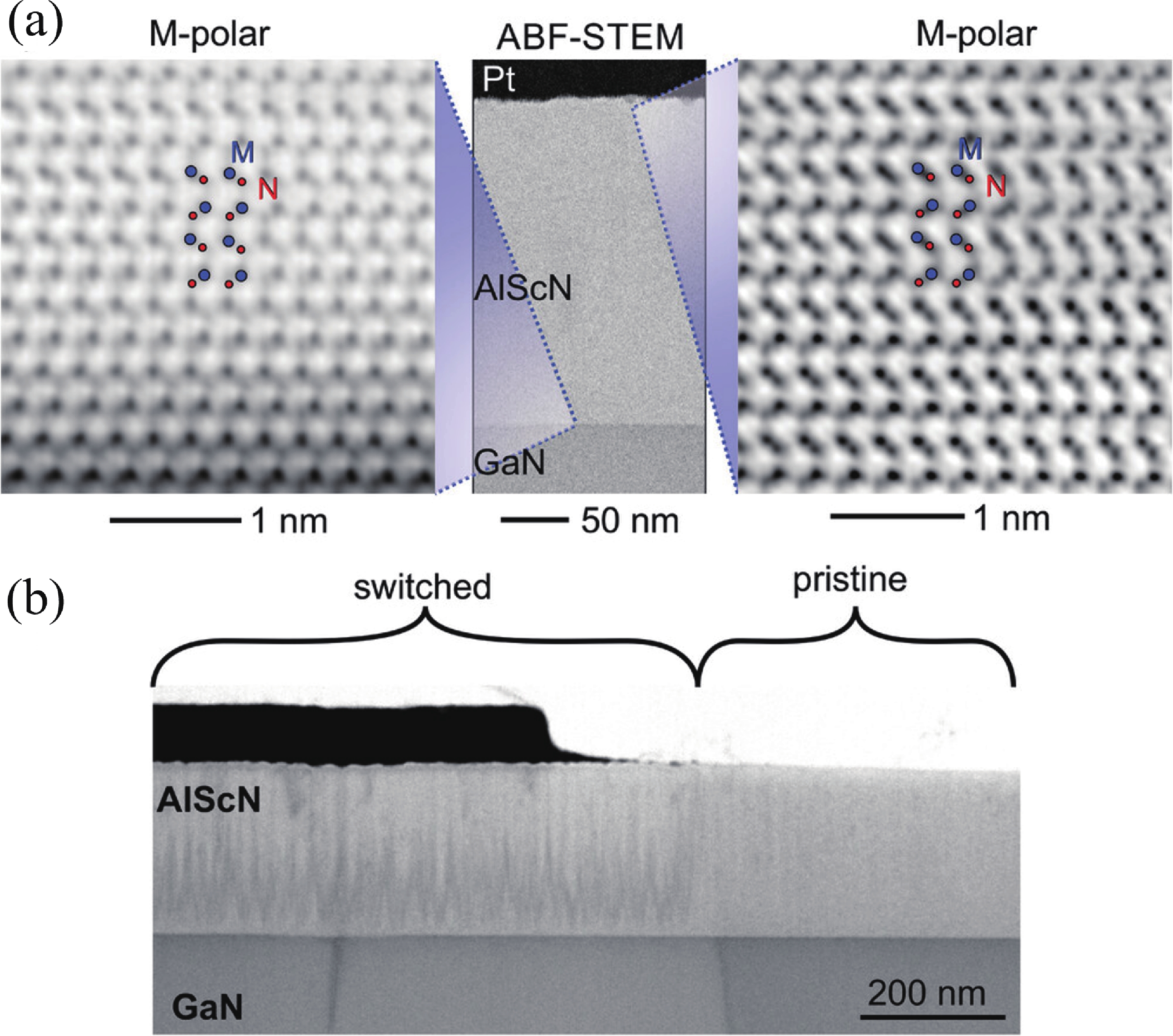
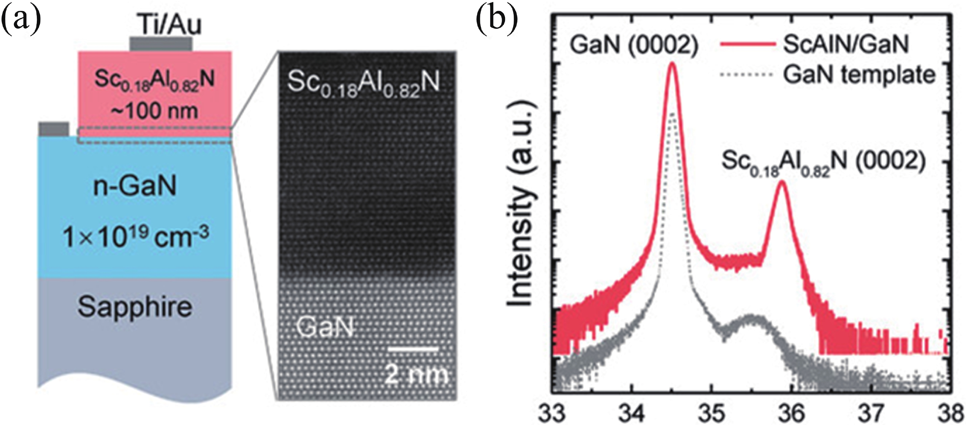
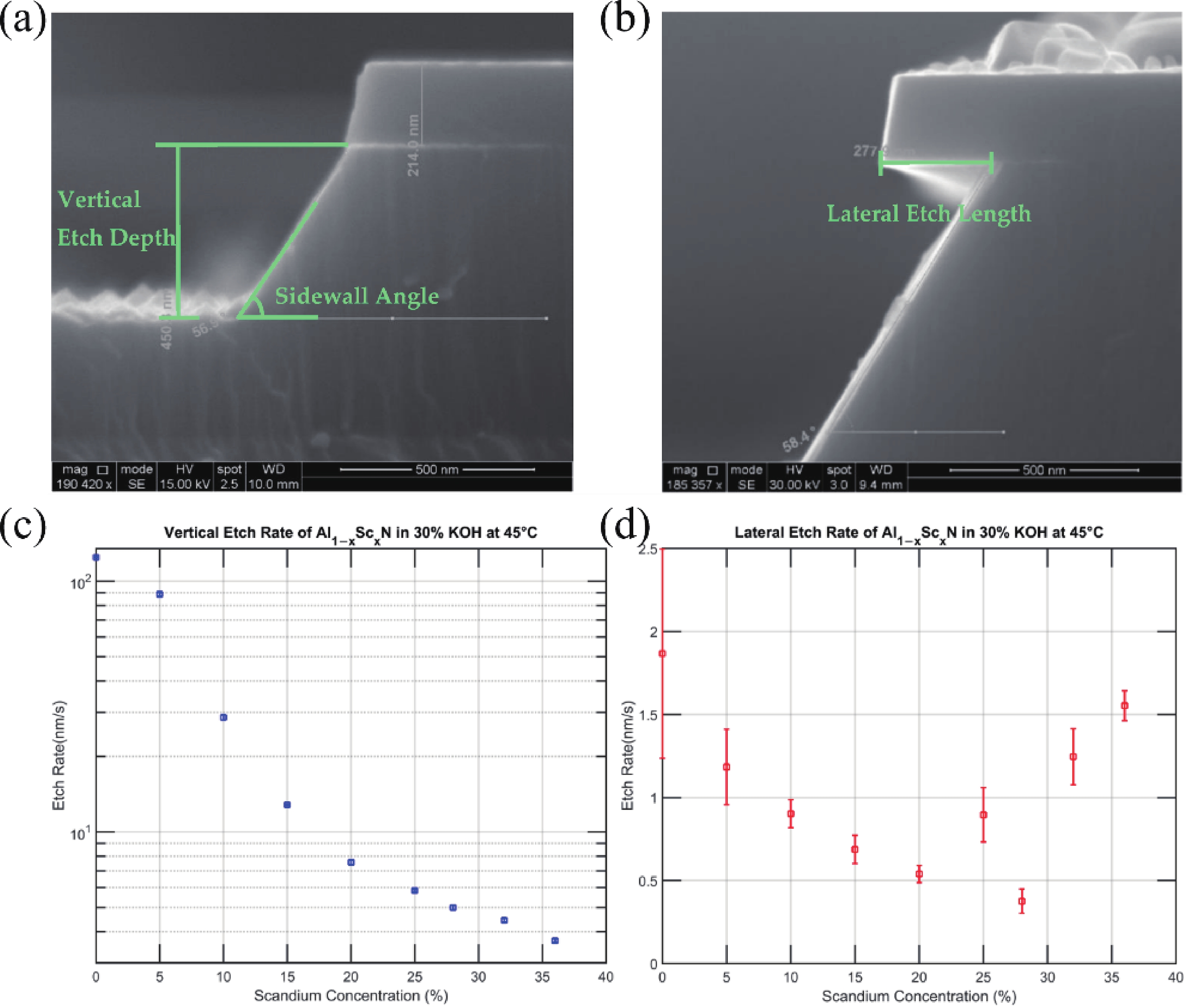
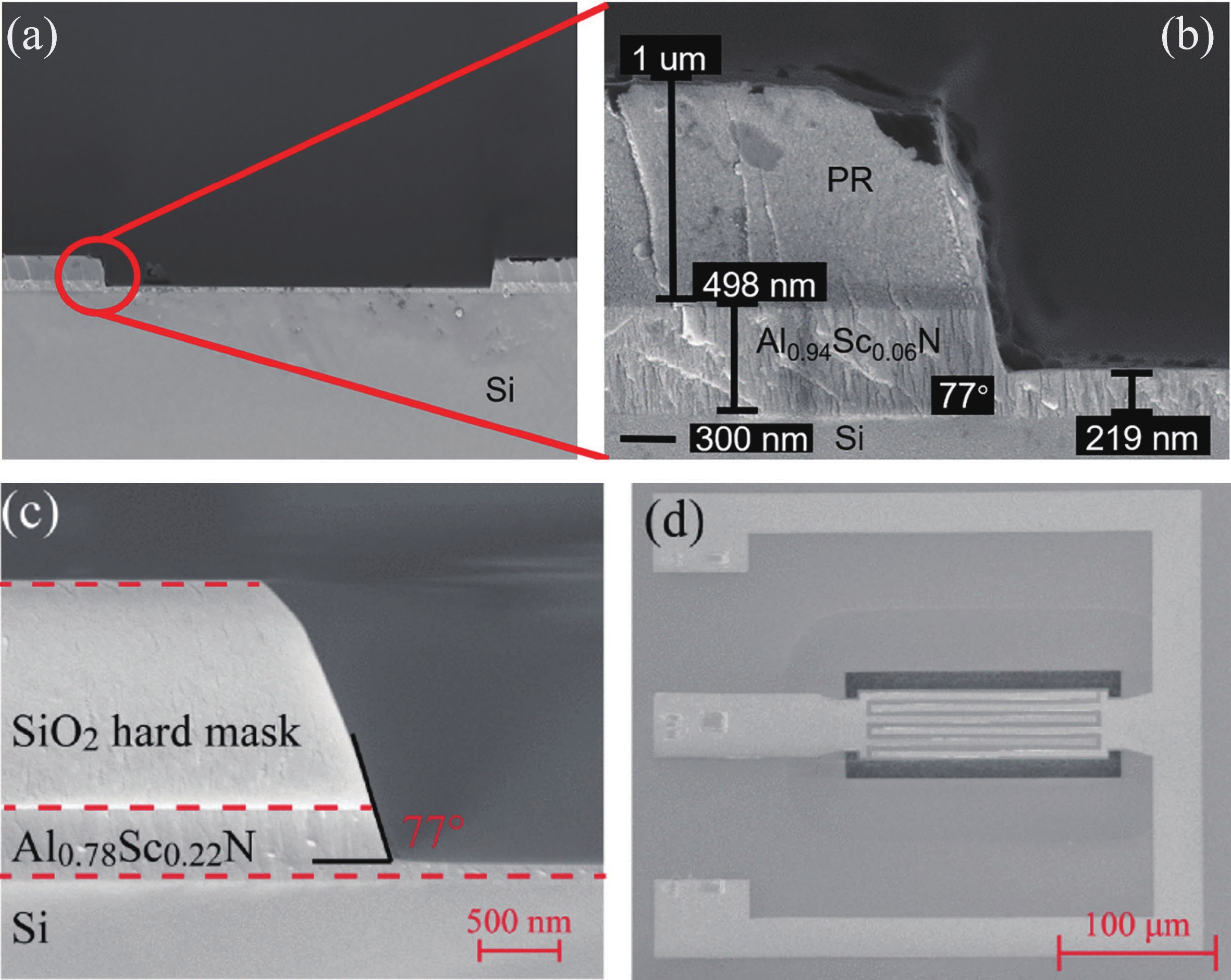
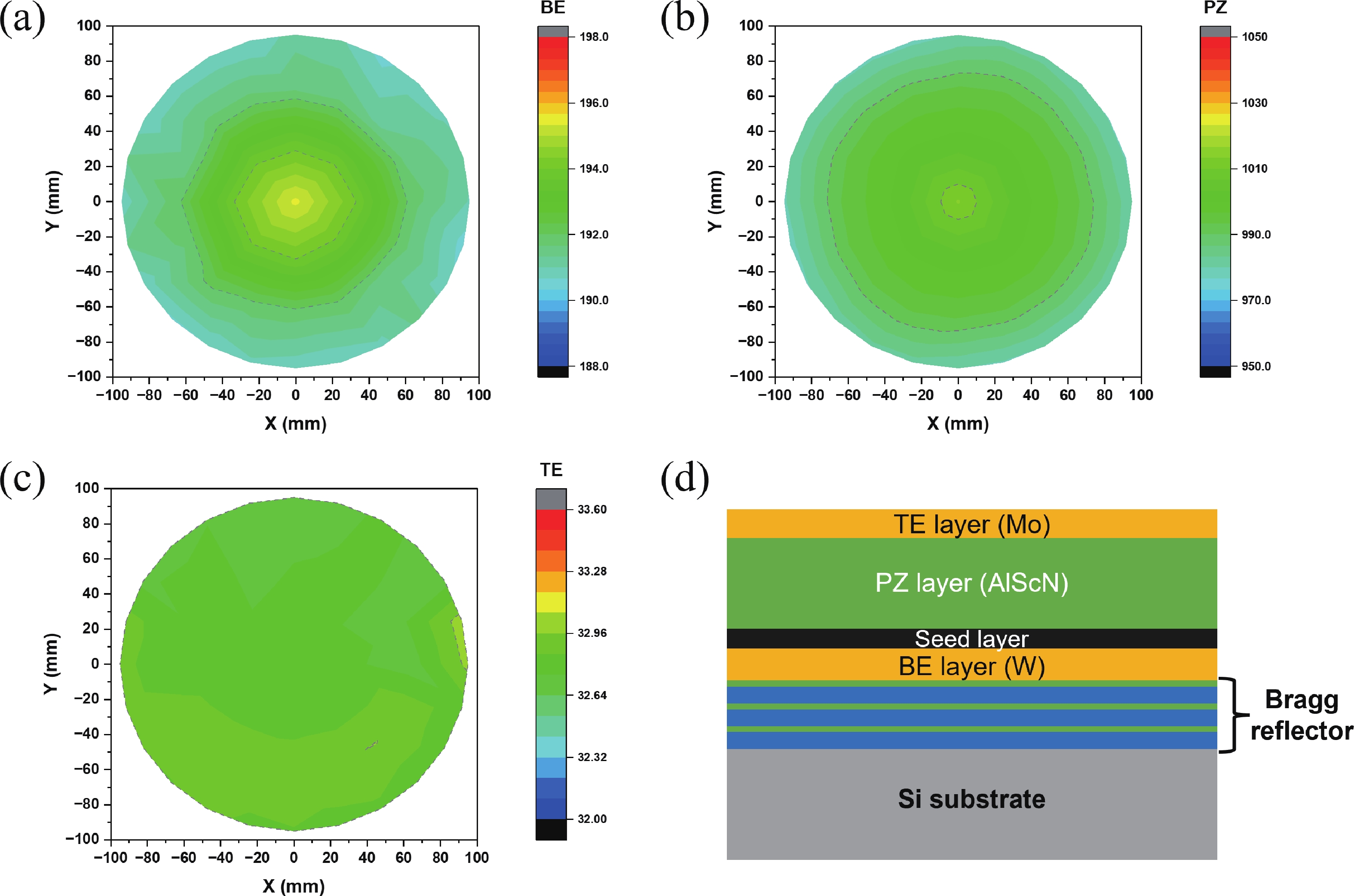
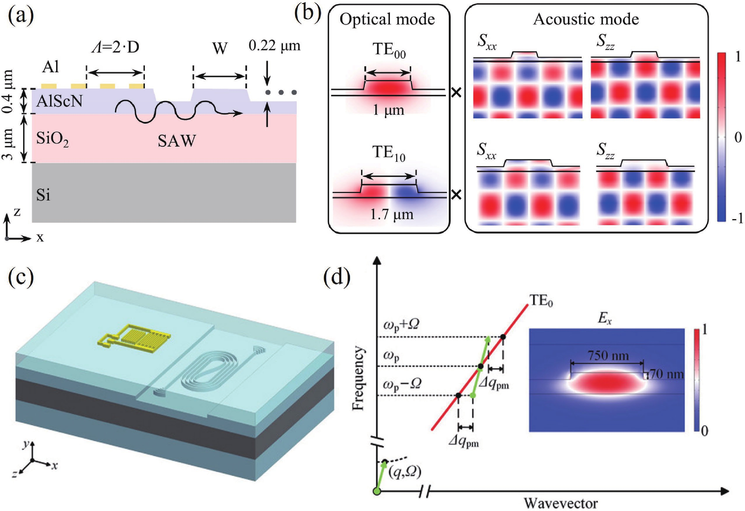
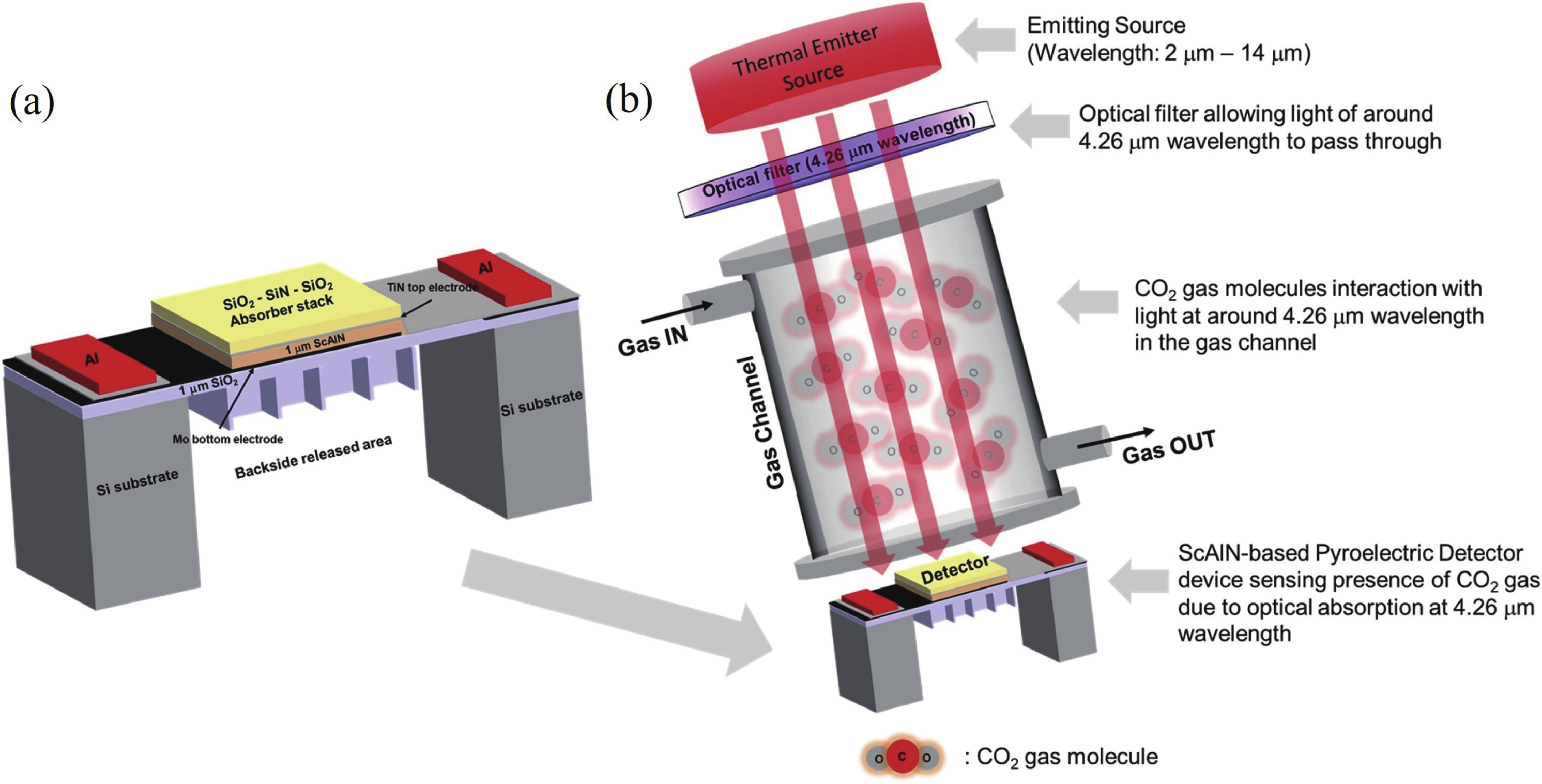
Aluminum scandium nitride (AlScN), an emerging Ⅲ-nitride semiconductor material, has attracted significant attention in recent years due to its exceptional piezoelectric properties, high thermal stability, tunable bandgap, and excellent compatibility with micro/nano fabrication. This paper systematically reviews the crystal structure, fundamental properties, and property modulation mechanisms of AlScN. It also summarizes recent progress in micro/nano fabrication technologies, including deposition, etching, and device integration. Furthermore, the applications of AlScN in diverse fields such as micro-electromechanical systems (MEMS), RF communications, energy conversion, optoelectronics and sensors are discussed. Finally, current challenges and promising future research directions for AlScN are outlined.
J. Semicond.
2026, 47(3): 032101 doi: 10.1088/1674-4926/25070029
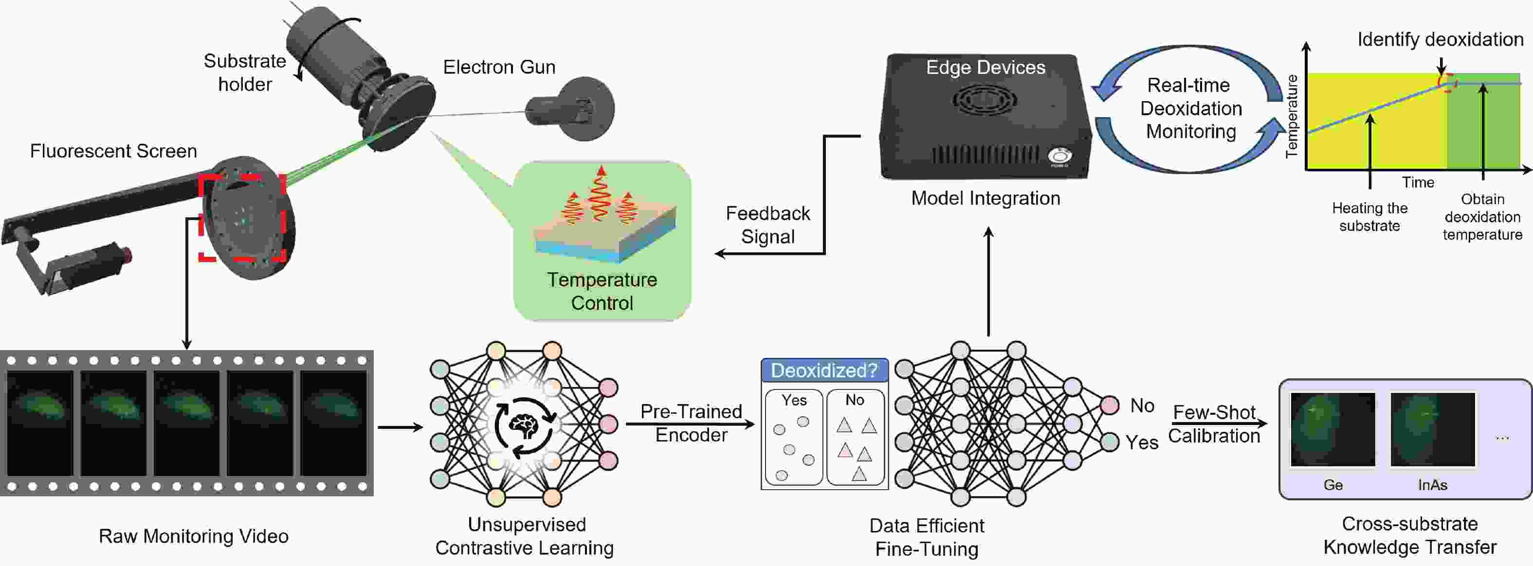
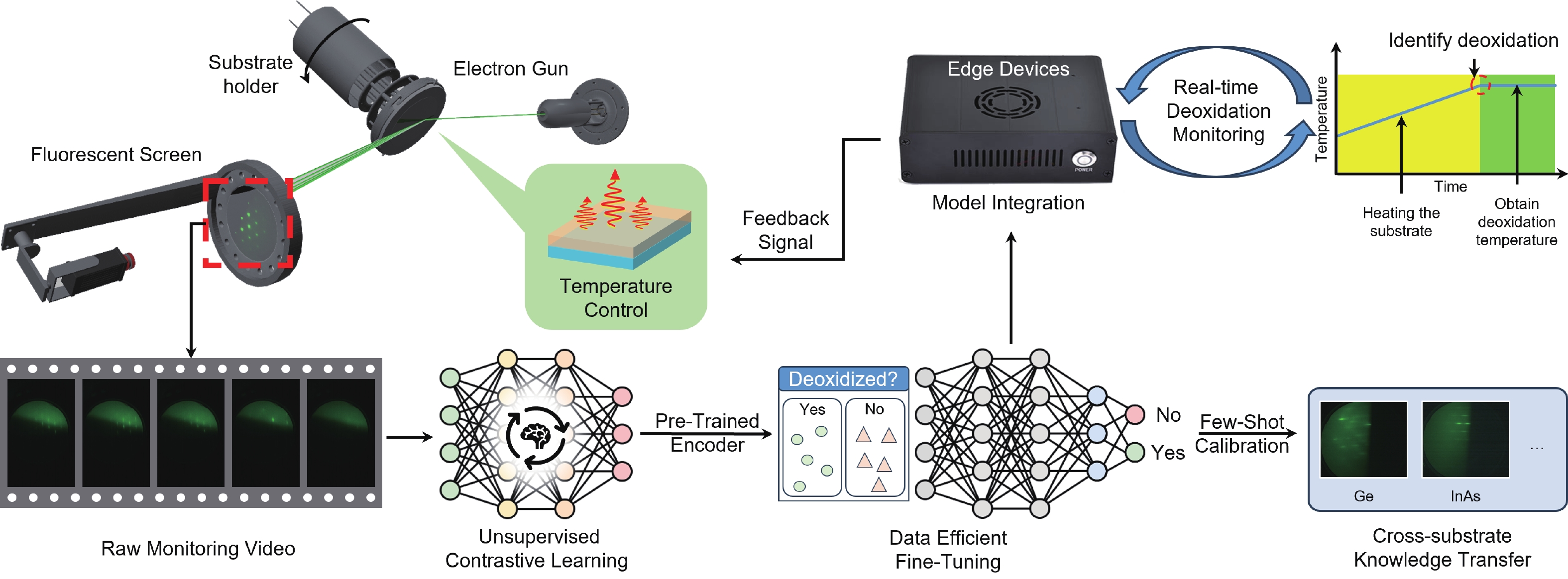
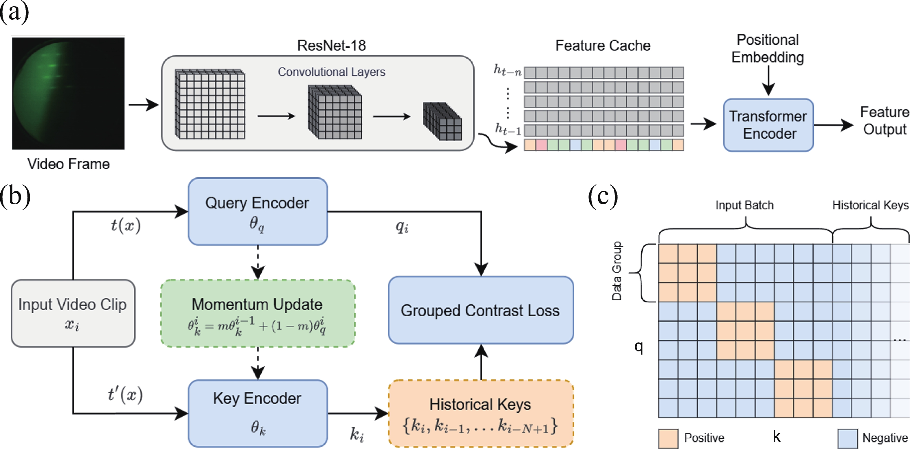
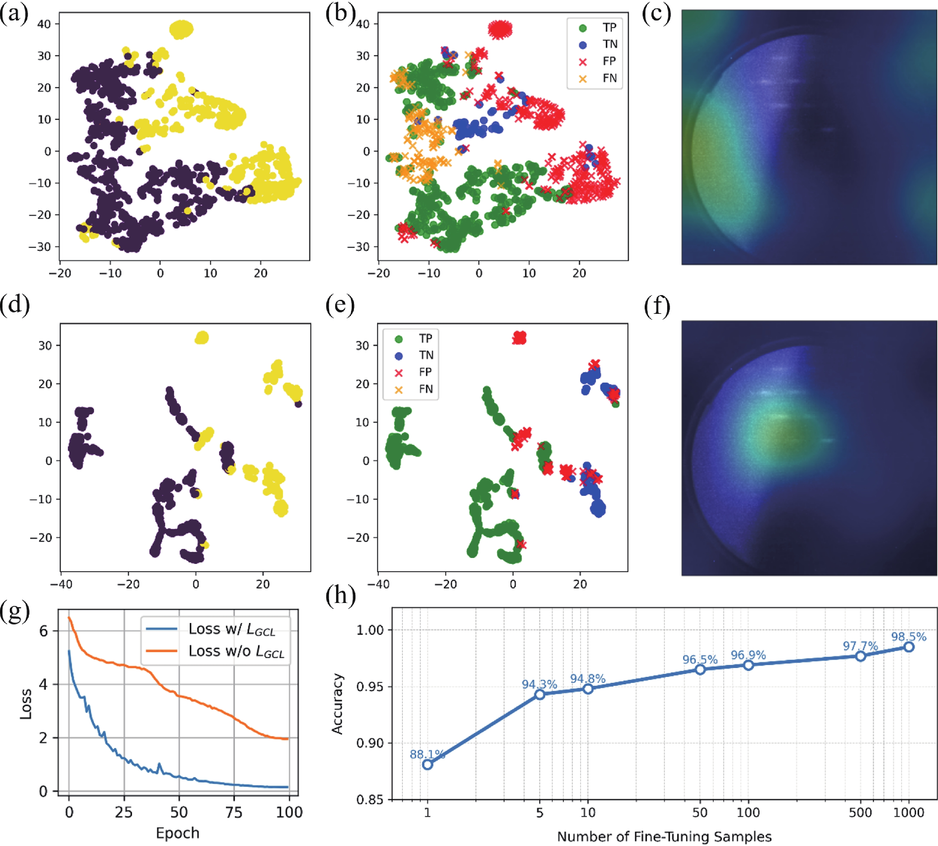
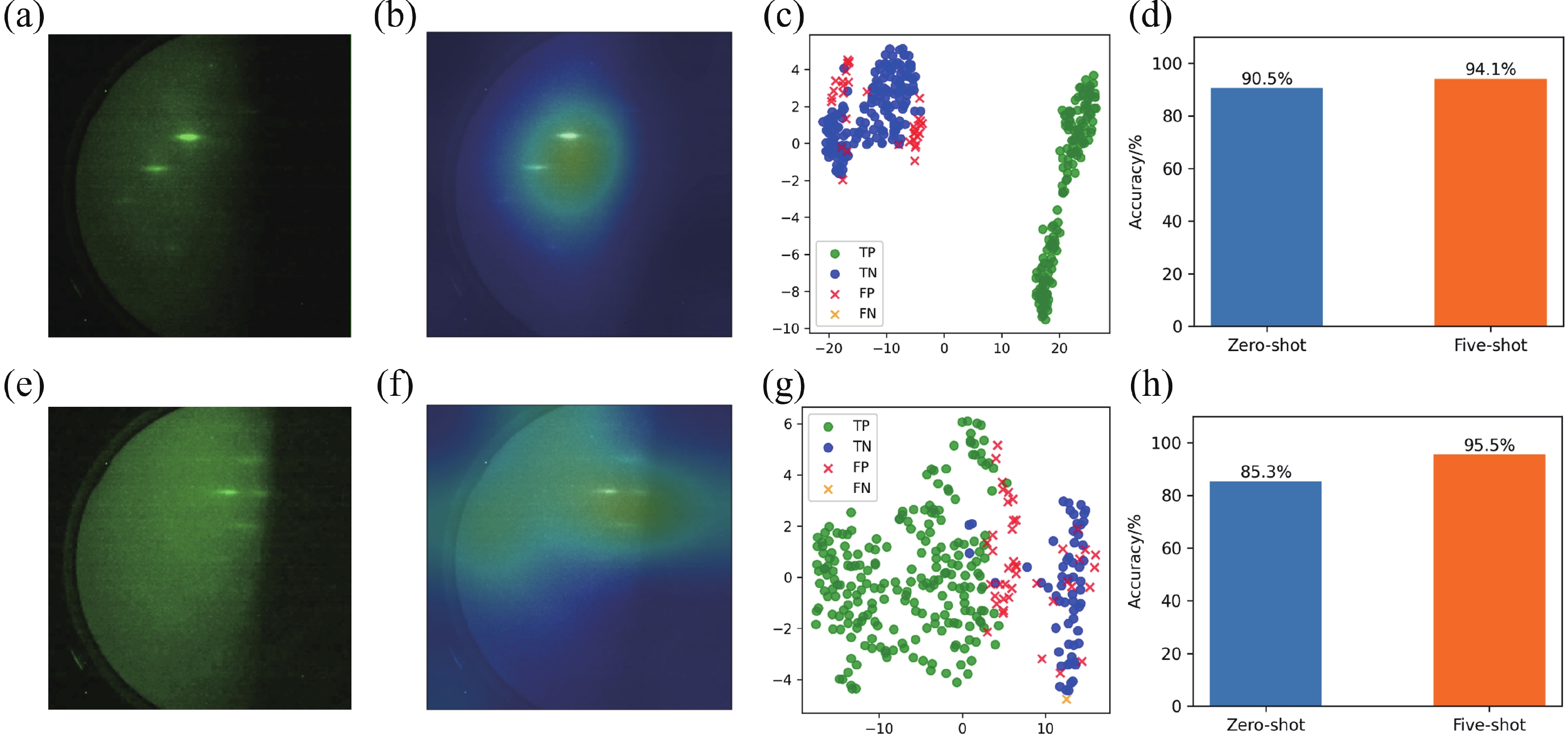
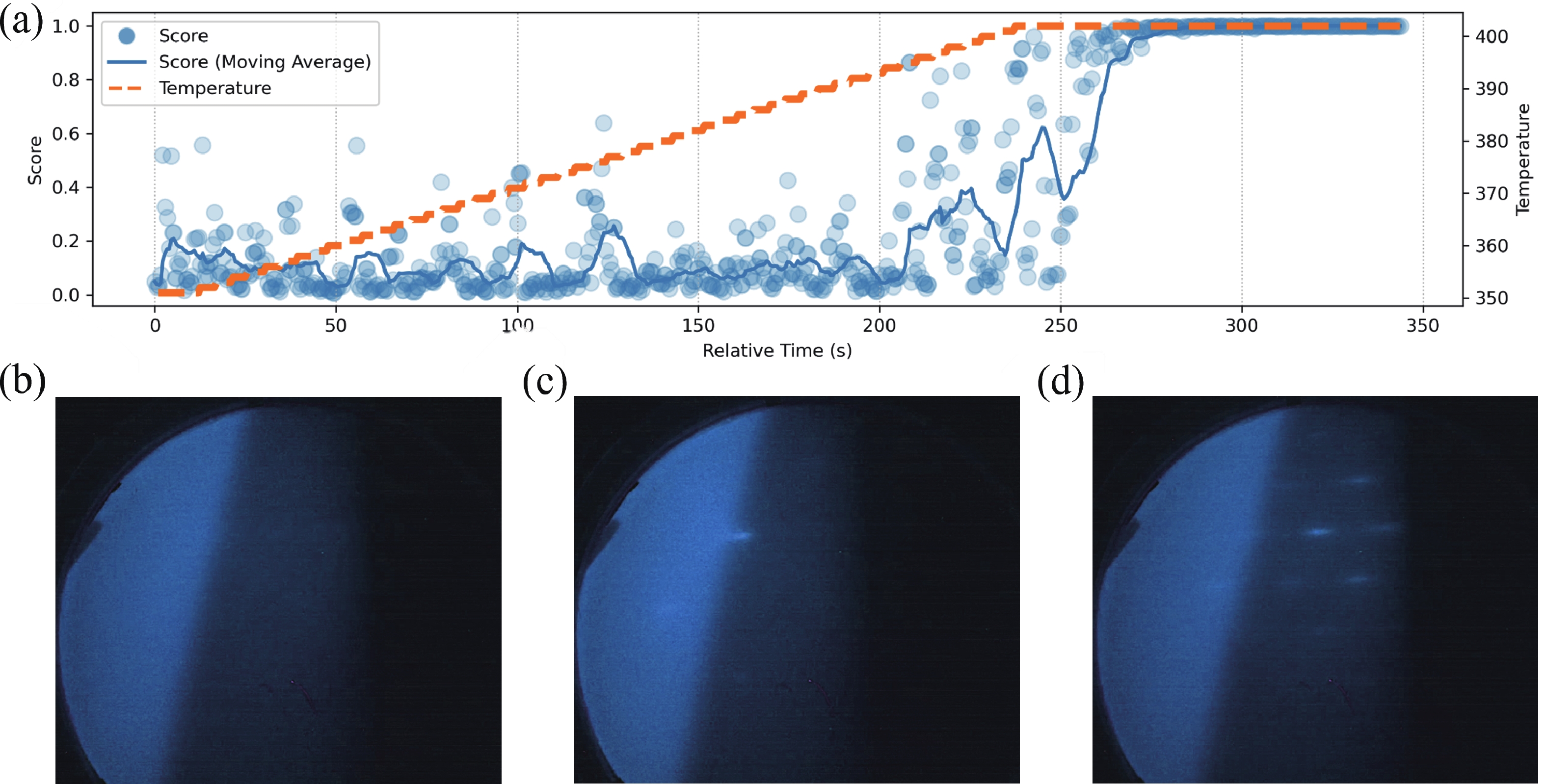
Accurate temperature control and effective oxide removal are essential for achieving high-quality epitaxial growth in molecular beam epitaxy (MBE). However, traditional methods often rely on manual identification of reflection high-energy electron diffraction (RHEED) patterns. This process is heavily influenced by the grower’s experience, leading to issues with reproducibility and limiting the potential for automation. In this report, we propose an unsupervised learning framework for real-time RHEED analysis during the deoxidation process. By incorporating temporal similarity constraints into contrastive learning, our model generates smooth and interpretable feature trajectories that illustrate transitions in the deoxidation state, thus eliminating the need for manual labeling. The model, pre-trained using grouped contrastive loss, shows significant improvement in RHEED feature boundary discrimination and localization of critical regions. We evaluated its generalizability through two transfer learning strategies: calibration-free clustering and few-shot fine-tuning. The pre-trained model achieved a clustering accuracy of 88.1% for GaAs deoxidation samples without additional labels and reached an accuracy of 94.3% to 95.5% after fine-tuning with just five sample pairs across GaAs, Ge, and InAs substrates. This framework is optimized for resource-constrained edge devices, allowing for real-time, plug-and-play integration with existing MBE systems and swift adaptation across various materials and equipment. This work paves the way for greater automation and improved reproducibility in semiconductor manufacturing.
J. Semicond.
2026, 47(3): 032102 doi: 10.1088/1674-4926/25070024
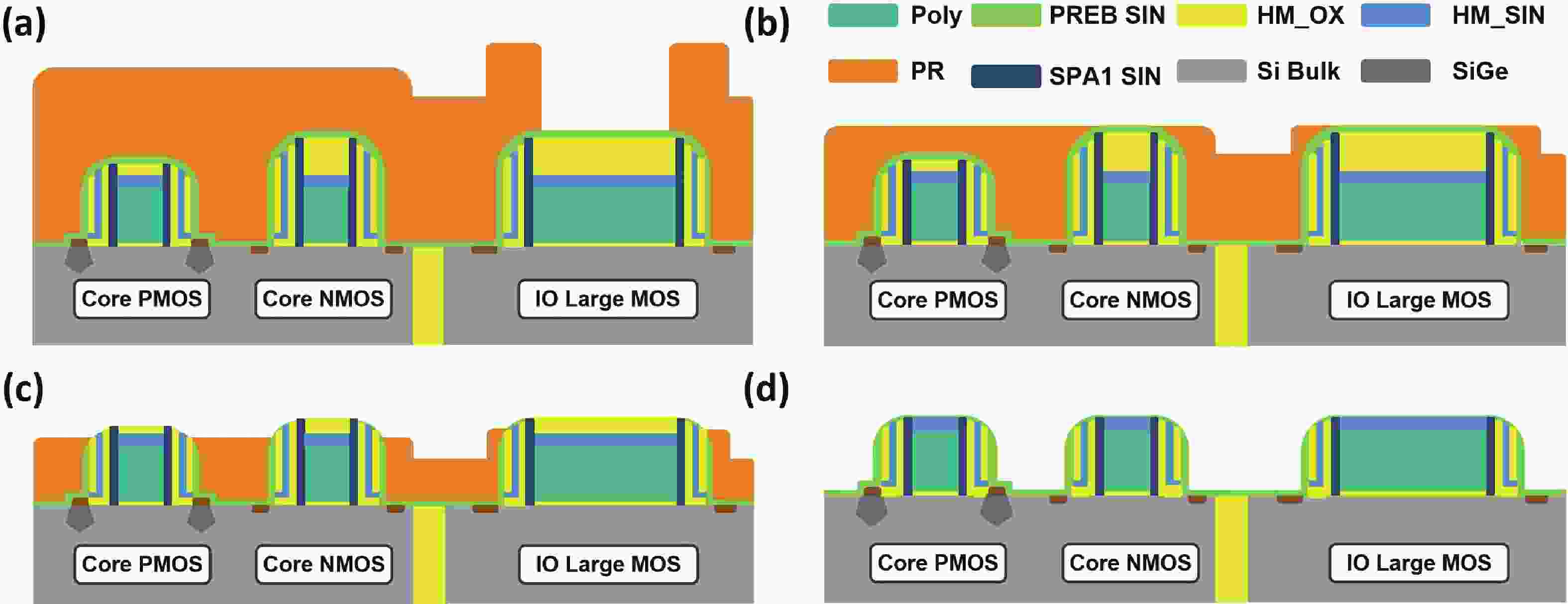
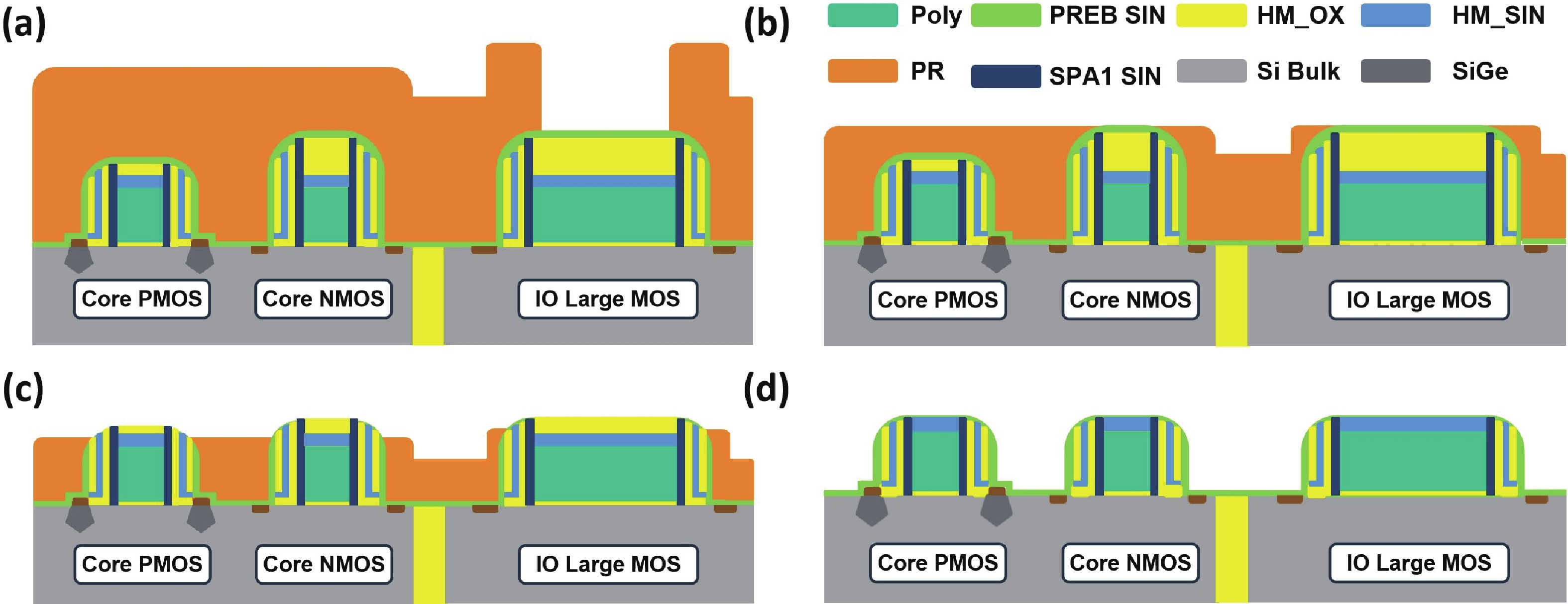
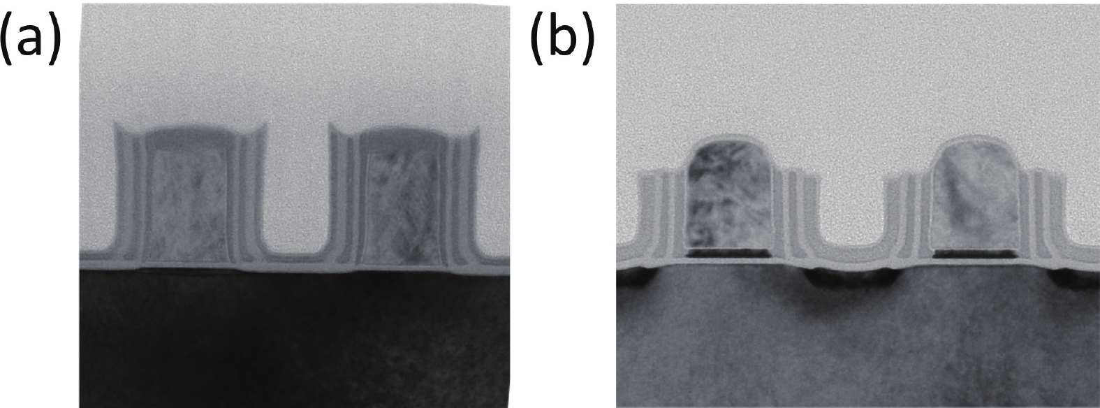
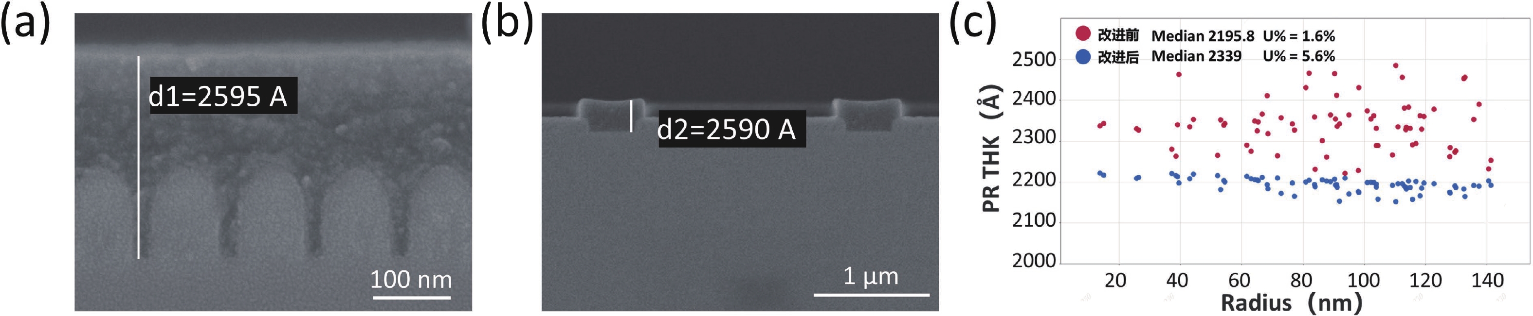
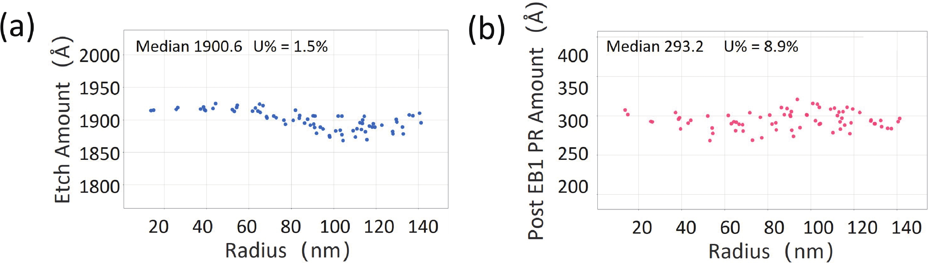
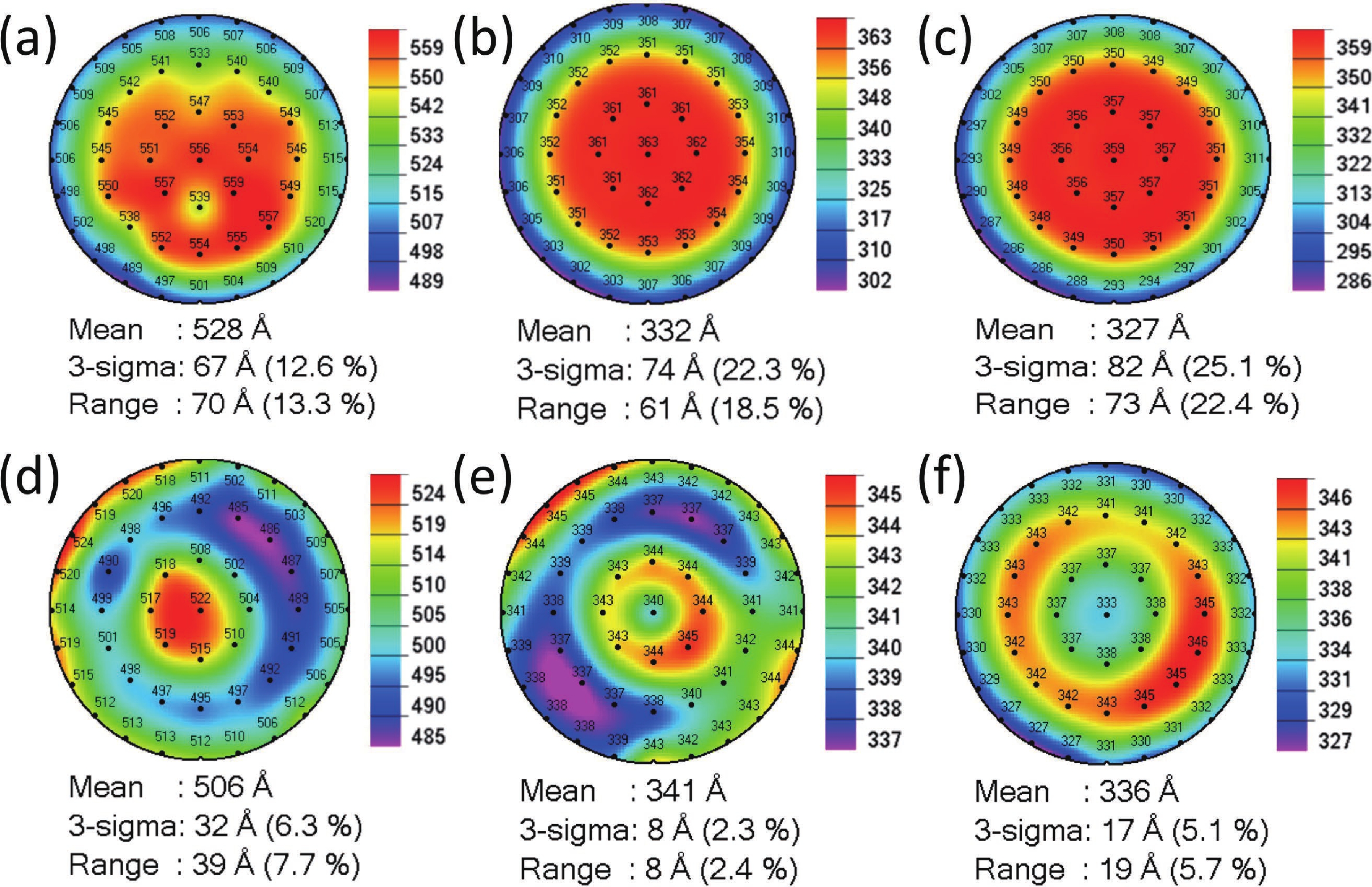
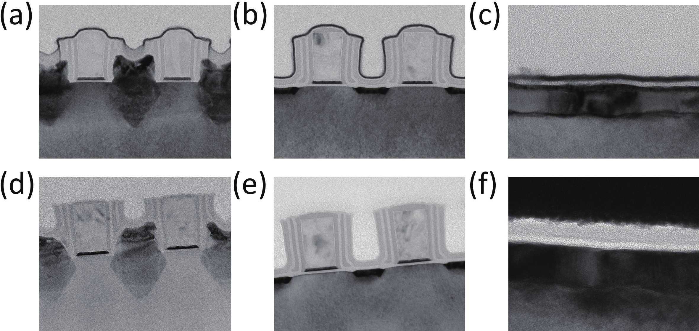
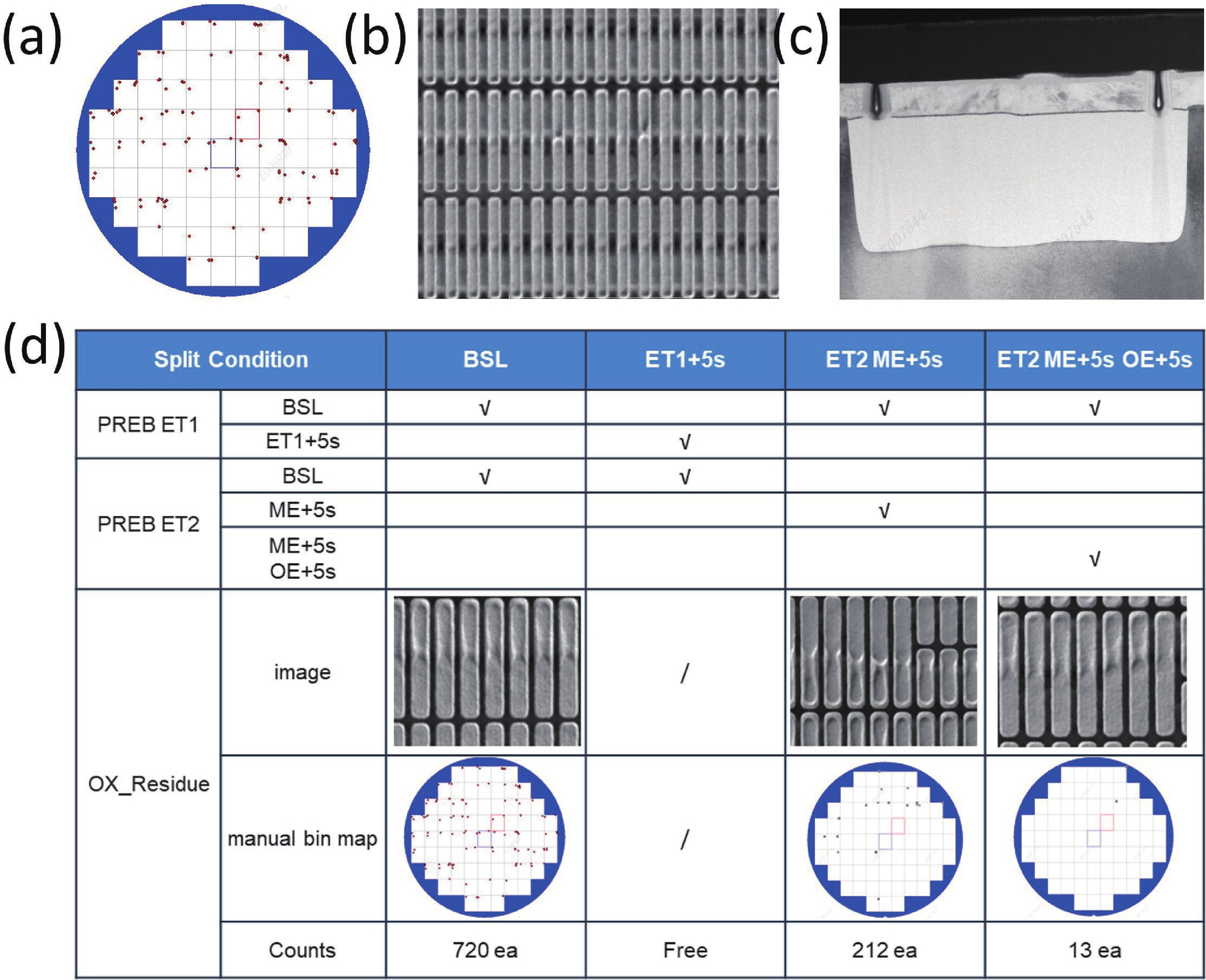
The introduction of high-k/metal gate (HK/MG) technology enables independent tuning of N-type metal−oxide−semiconductor (NMOS) and P-type metal−oxide−semiconductor (PMOS) threshold voltages, facilitating advanced nodes and improving overall chip performance. However, severe pattern loading effects during PMOS device fabrication pose challenges in dummy poly removal. This work reports the optimization of the photoresist etch back (PREB) process, providing a wider process window for subsequent AL CMP. By tuning the PR coating uniformity to 1.6% and applying four-zone electrostatic chuck (ESC) temperature control, the wafer-level uniformities of PR, SiN, and SiO2 were reduced to 6.3%, 2.3%, and 5.1%, respectively. An optimized over etch (OE) recipe with a high selectivity of PR : SiN : SiO2 ≈ 1 : 1 : 6 effectively balanced gate height loading between N- and PMOS regions. Furthermore, precise EB1 time tuning enabled defect removal, while advanced KLA inspection ensured early detection of critical failure modes. Collectively, these measures establish a robust and stable PREB process for advanced logic device fabrication.
J. Semicond.
2026, 47(3): 032301 doi: 10.1088/1674-4926/25060033
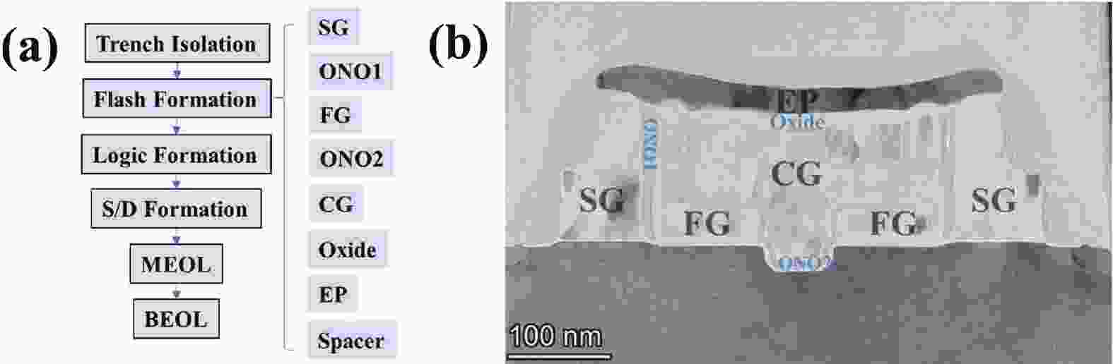
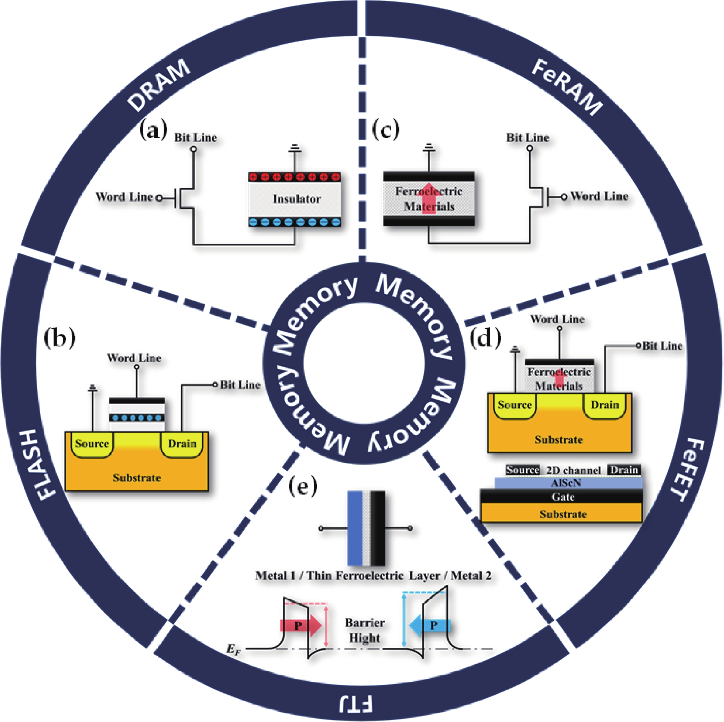
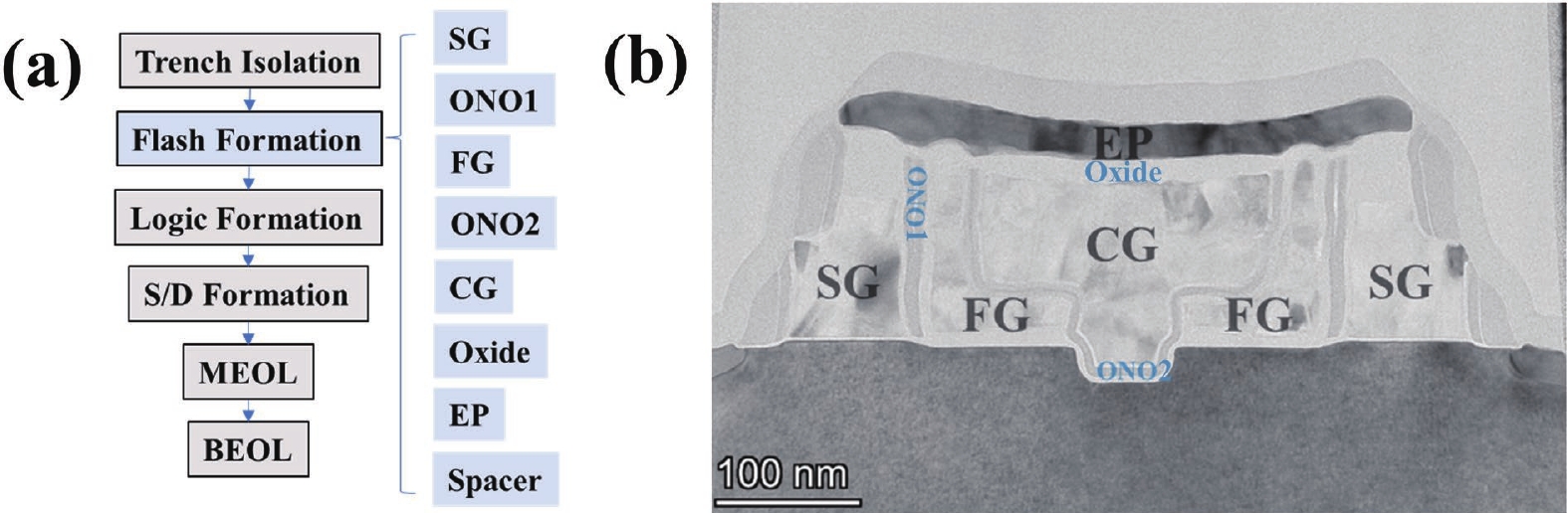
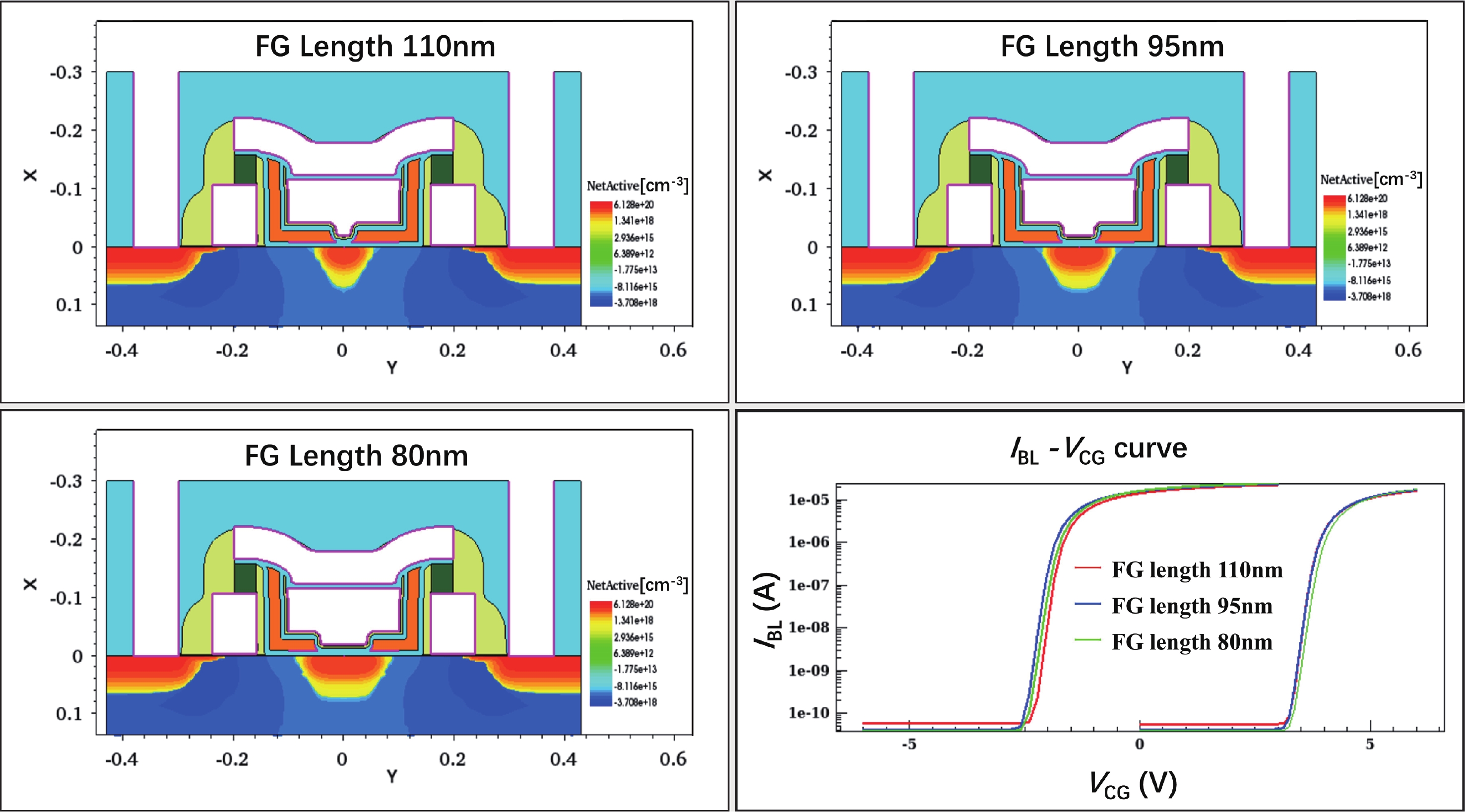
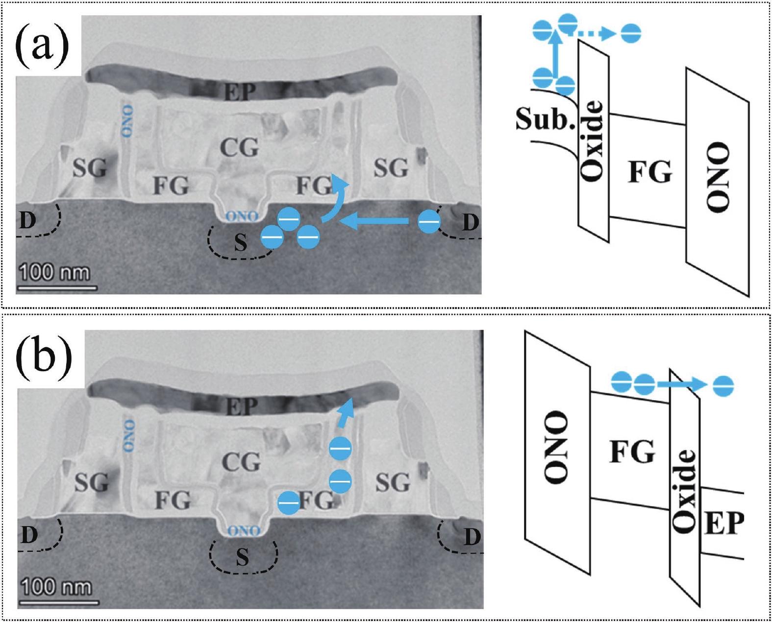
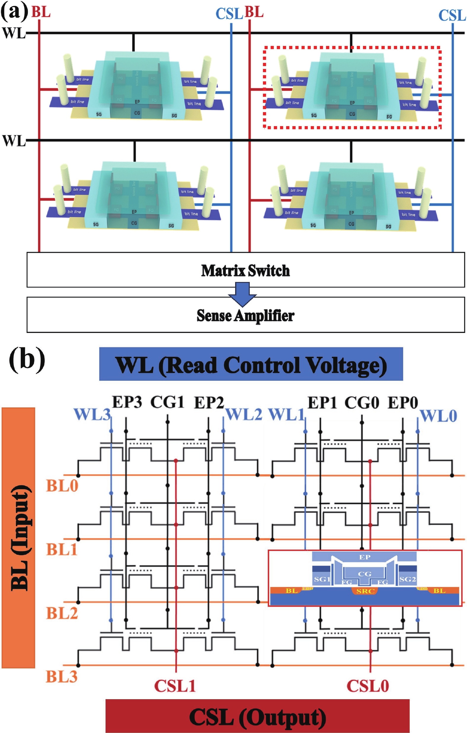
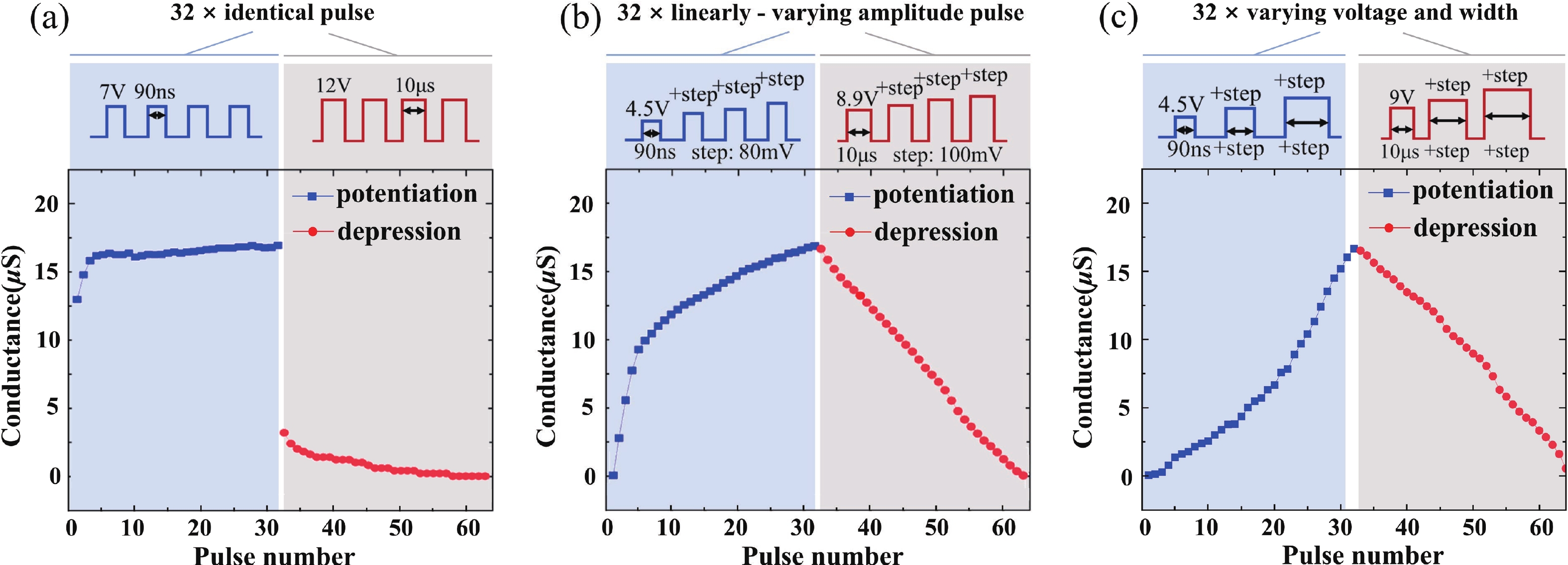
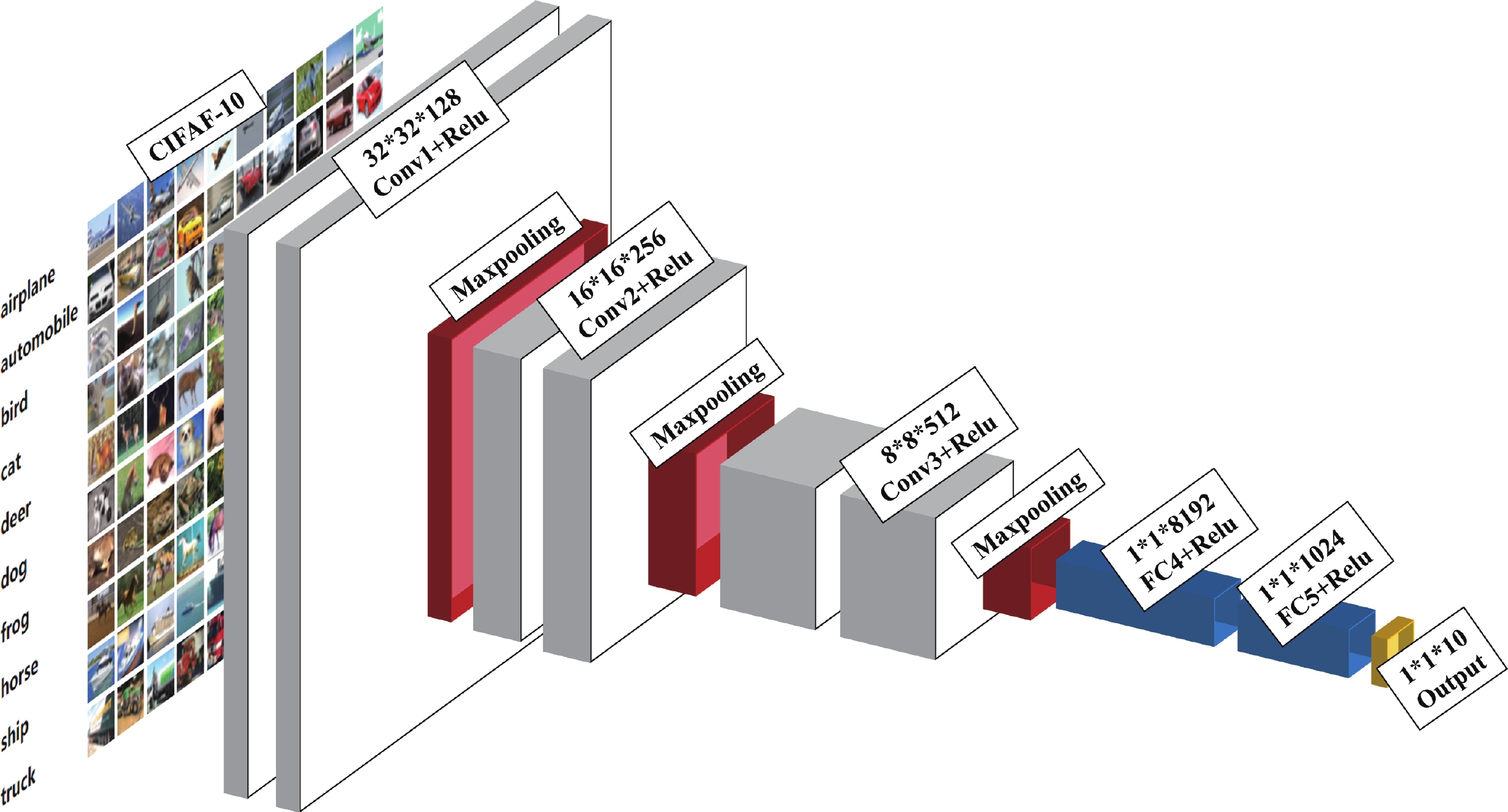
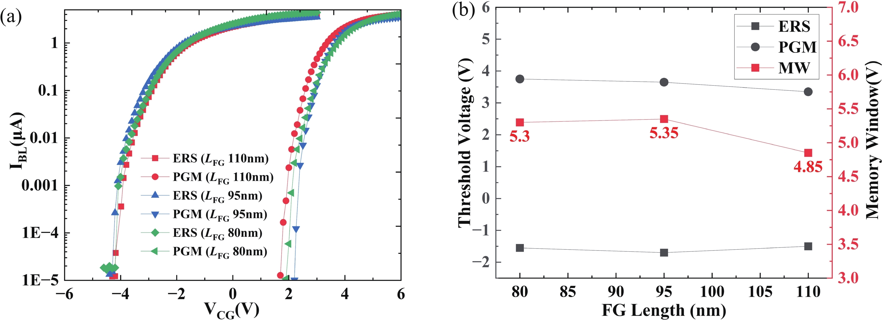
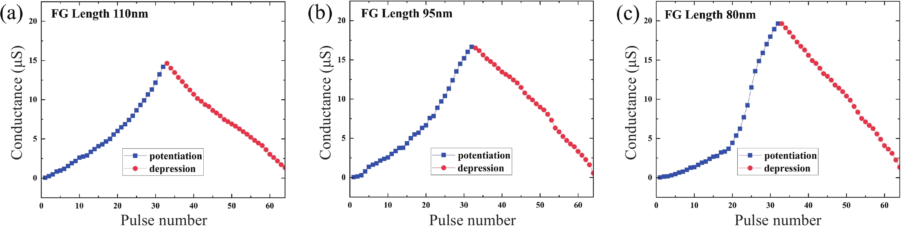
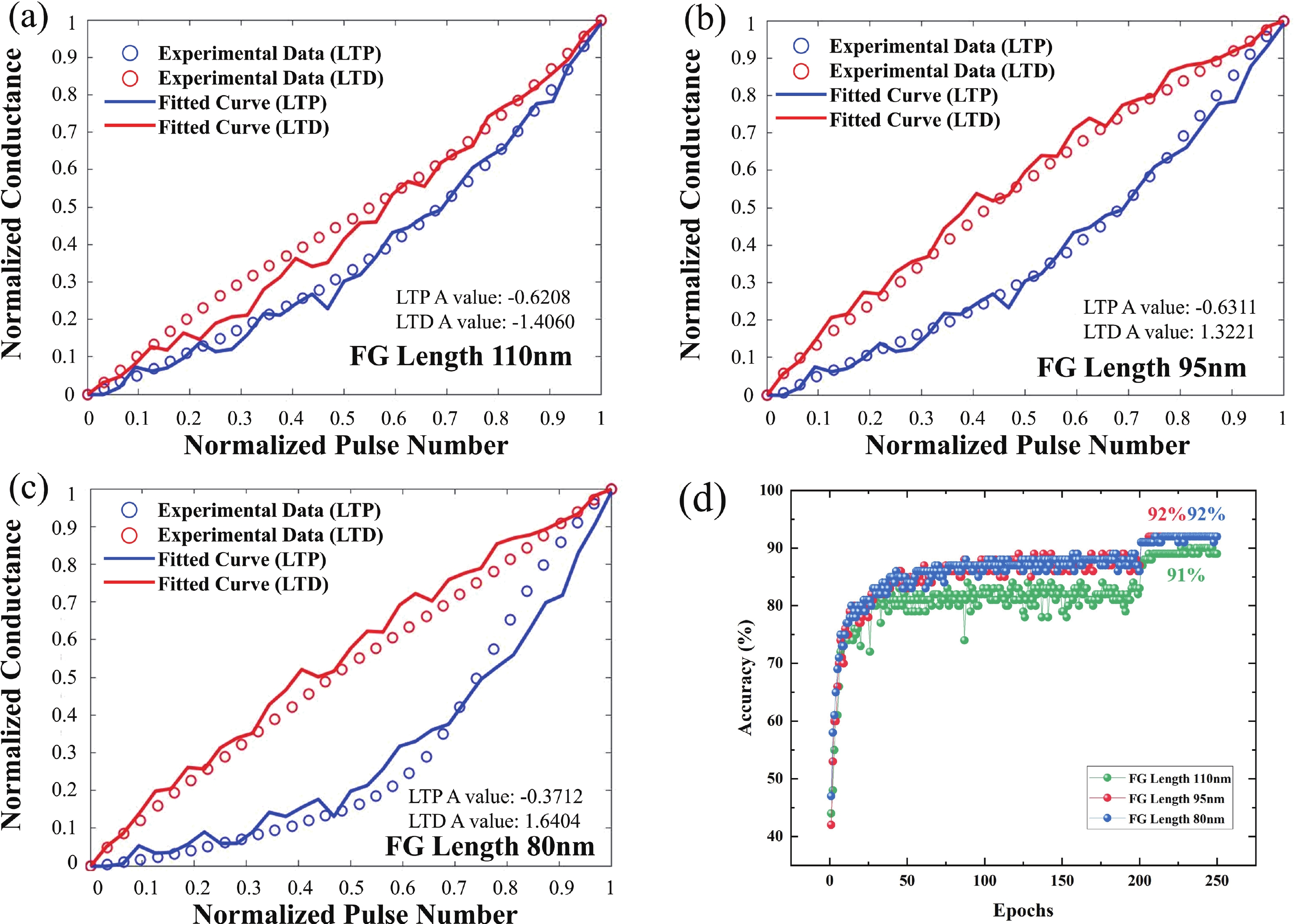
The escalating need for high-performance artificial intelligence (AI) computing intensifies the "memory bottleneck" of the von Neumann architecture, prompting extensive exploration of computation-in-memory (CIM) solutions. This study is centered on the optimization of a high-efficiency, low-power "L"-shaped split-gate floating-gate (FG) memory for CIM applications. Fabricated on a 55 nm CMOS platform, the memory devices were systematically investigated through wafer acceptance test (WAT), Sentaurus™ simulations and comprehensive evaluations with the DNN + NeuroSim Framework V2.0. Among devices with diverse FG lengths, the 95-nm FG variant exhibits outstanding performance: it achieves a 5.35 V memory window, reaches a maximum conductance of 16.7 μS with excellent linearity under the varying voltage and width pulse scheme (VWPS), realizes 32-state multi-level storage, and attains a 92% training accuracy on the CIFAR-10 dataset using the VGG8 neural network.
J. Semicond.
2026, 47(3): 032302 doi: 10.1088/1674-4926/25100007
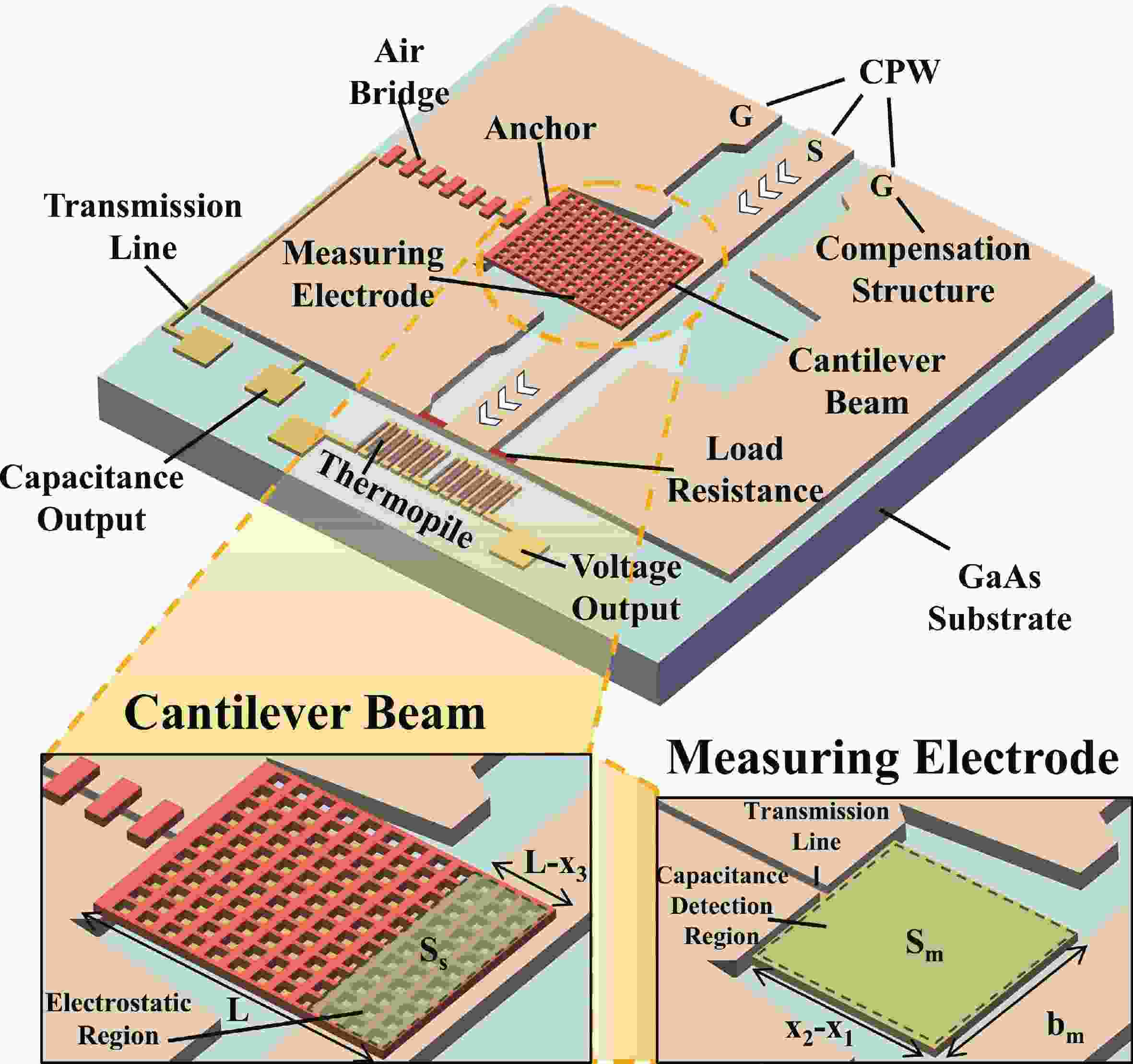
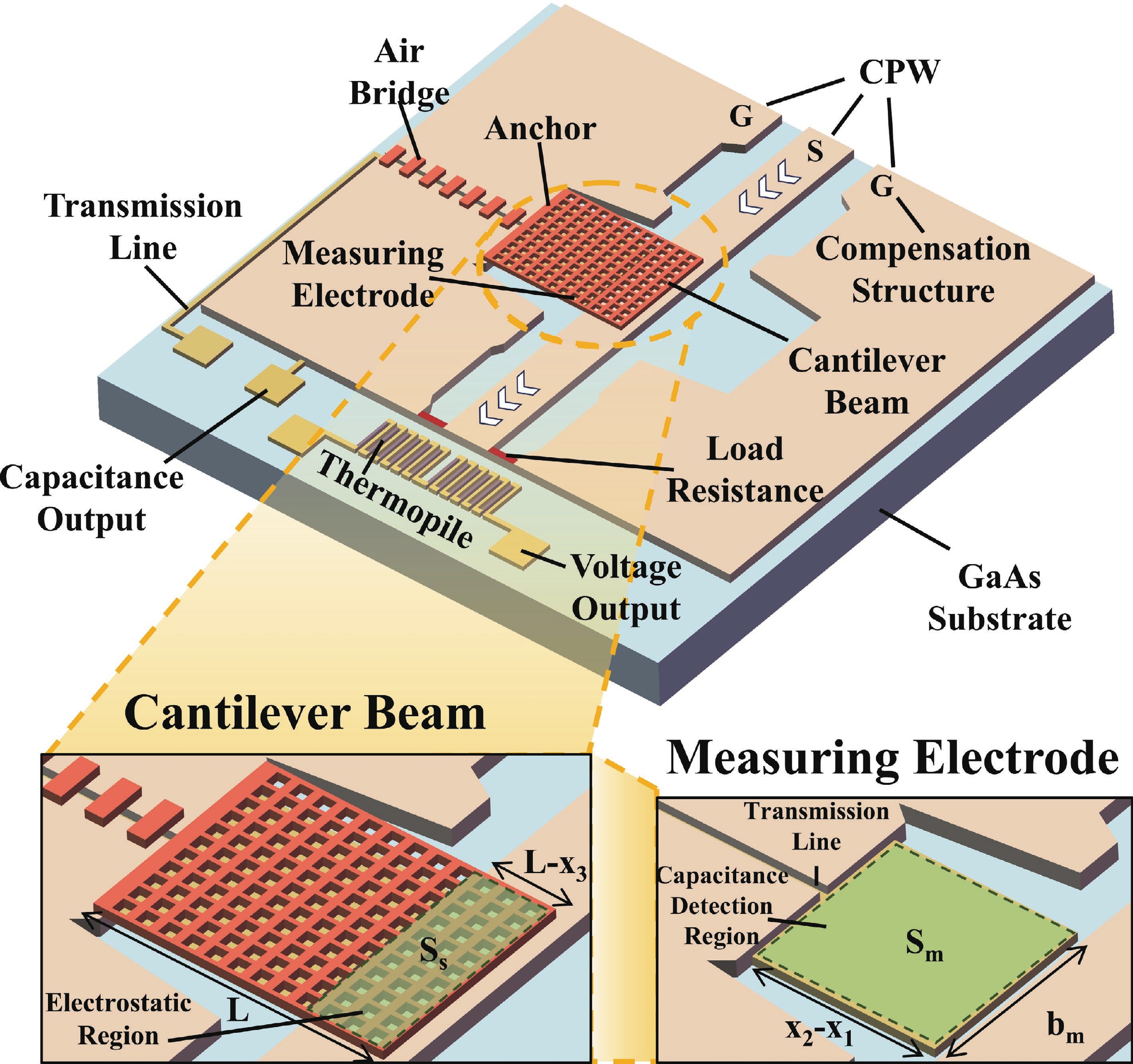
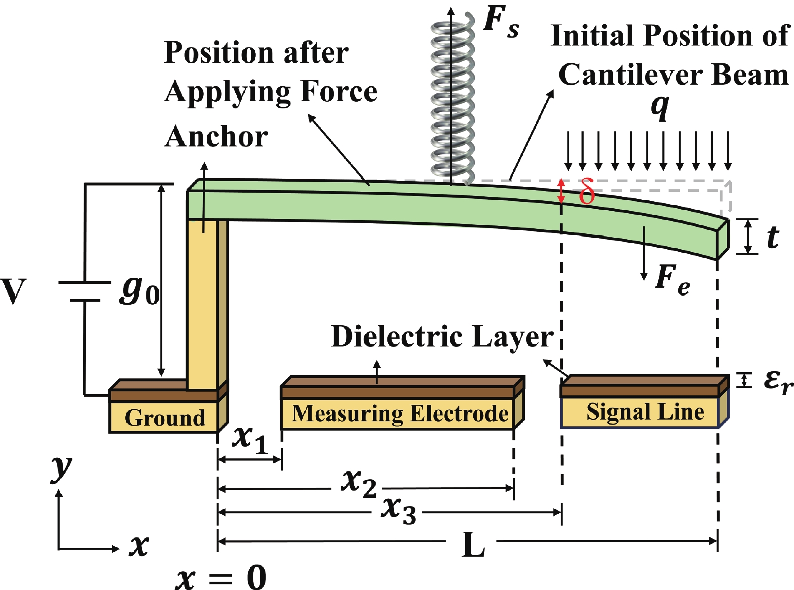
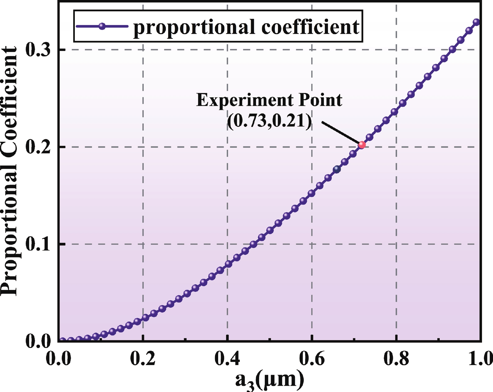
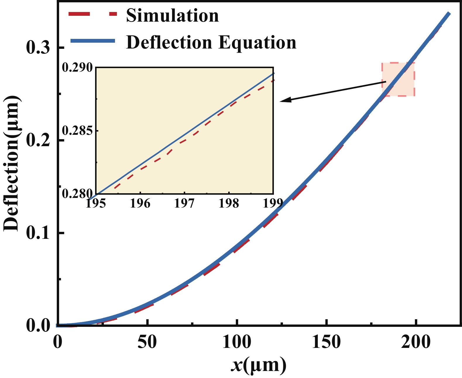
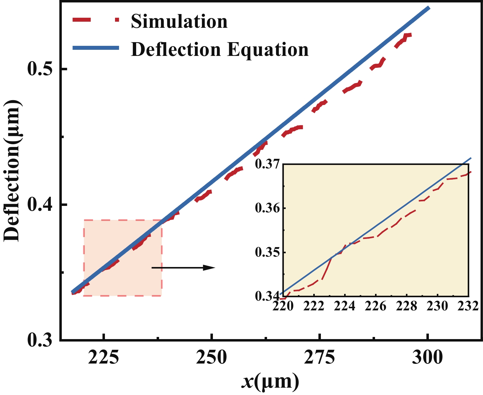
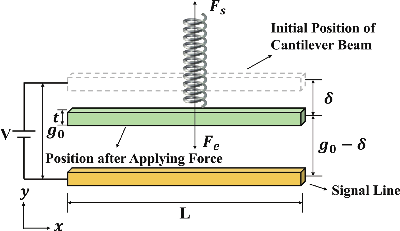
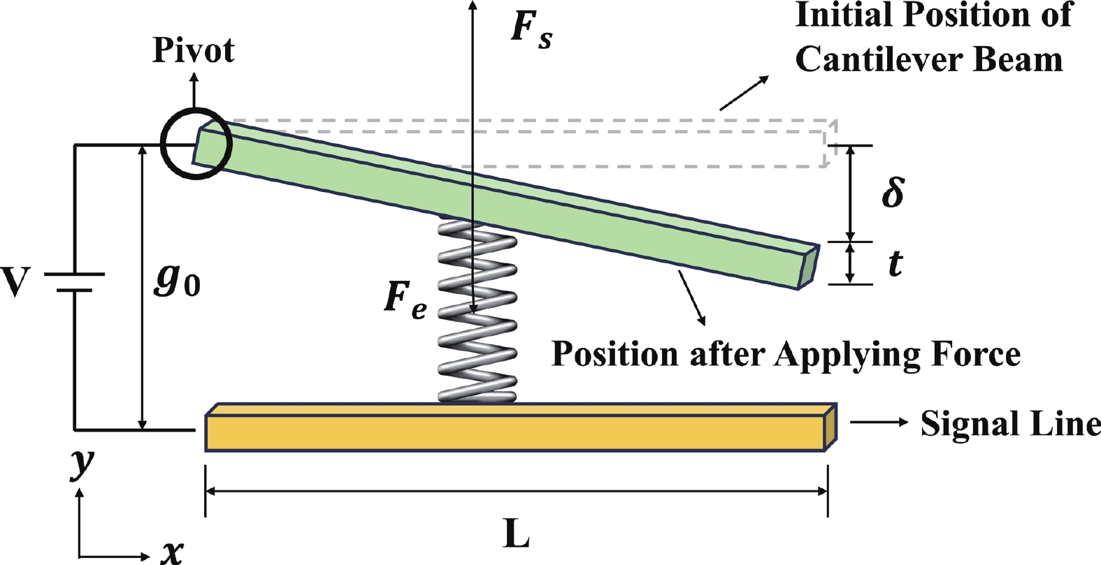
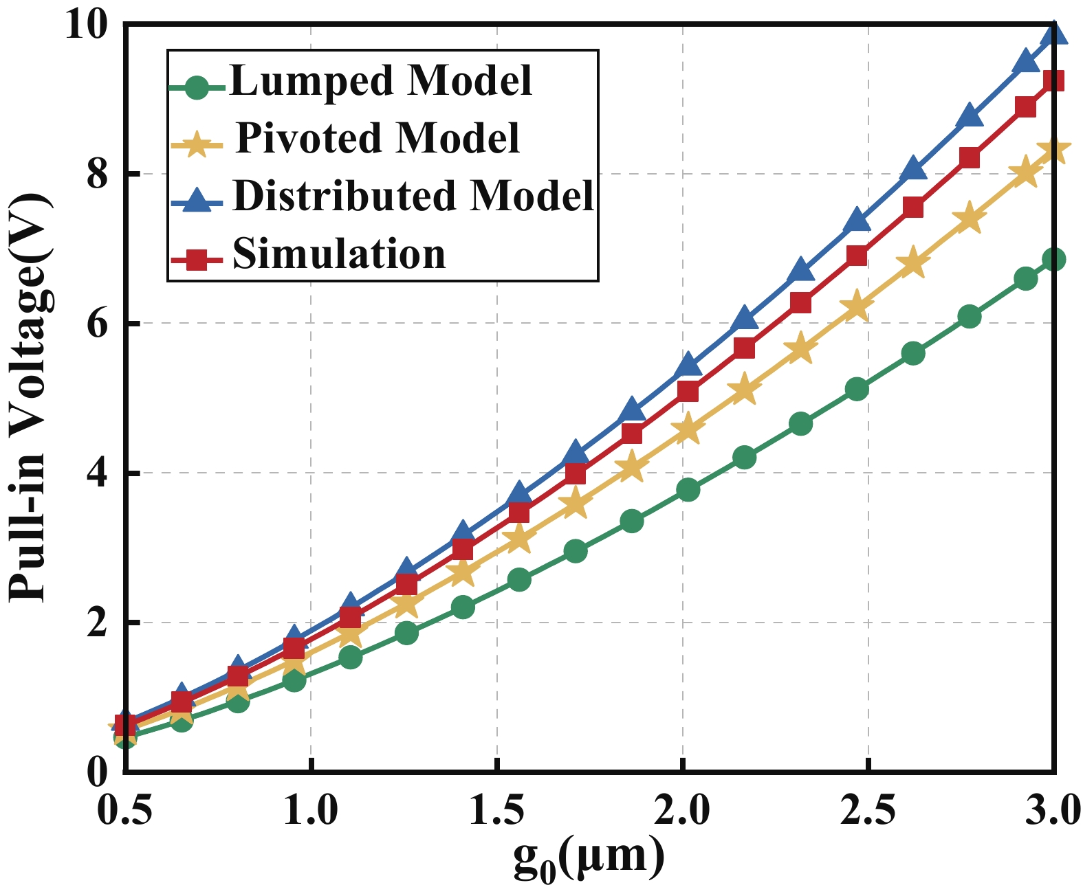
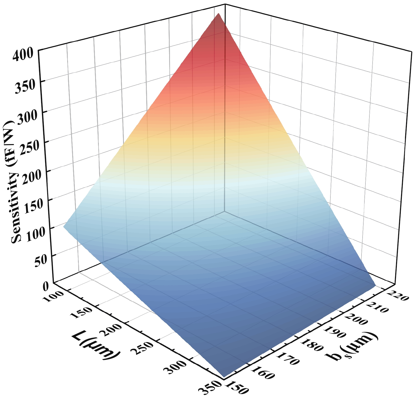
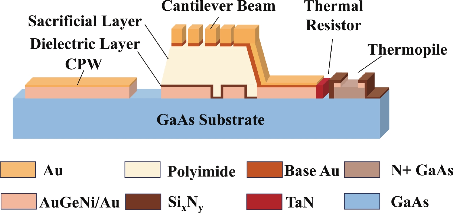
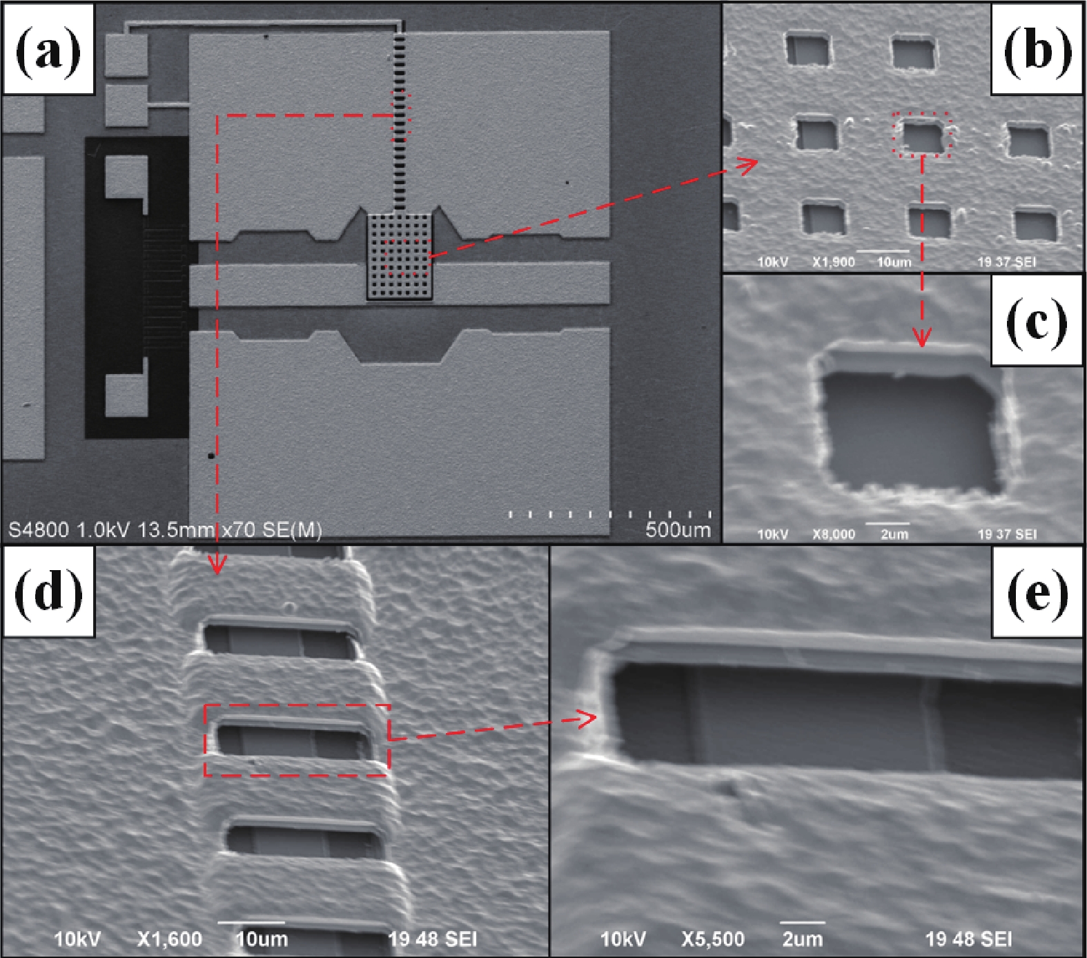
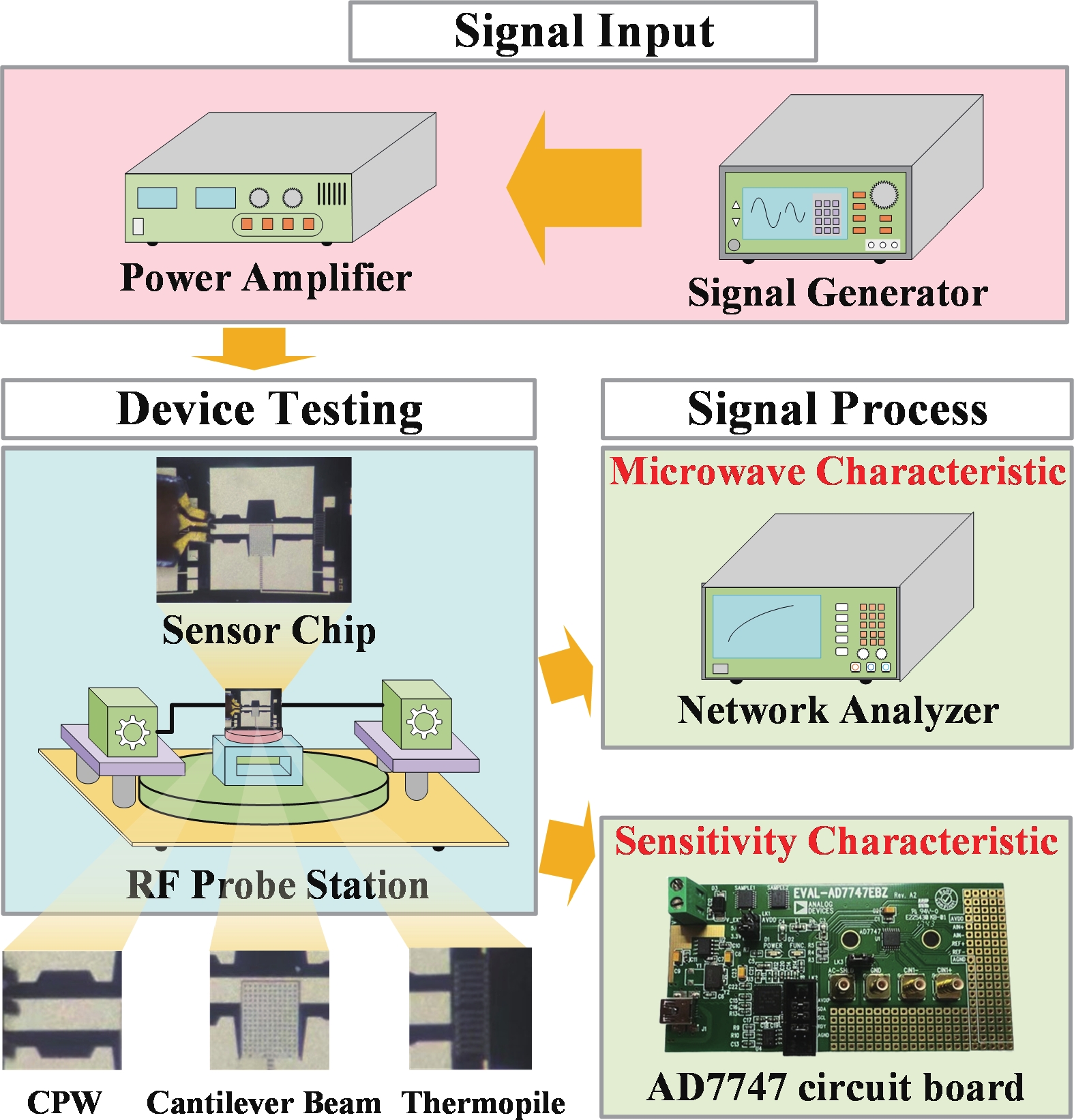
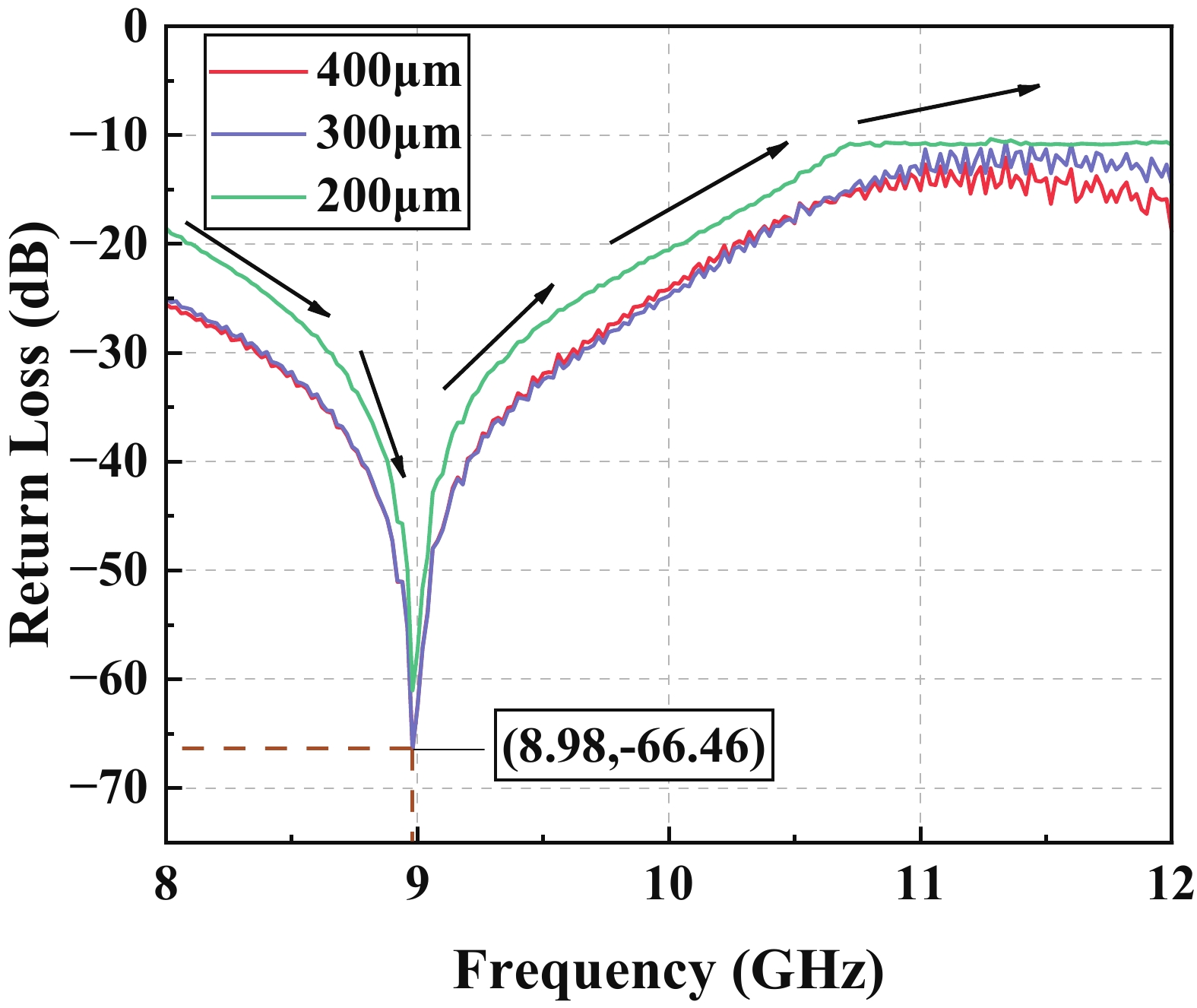
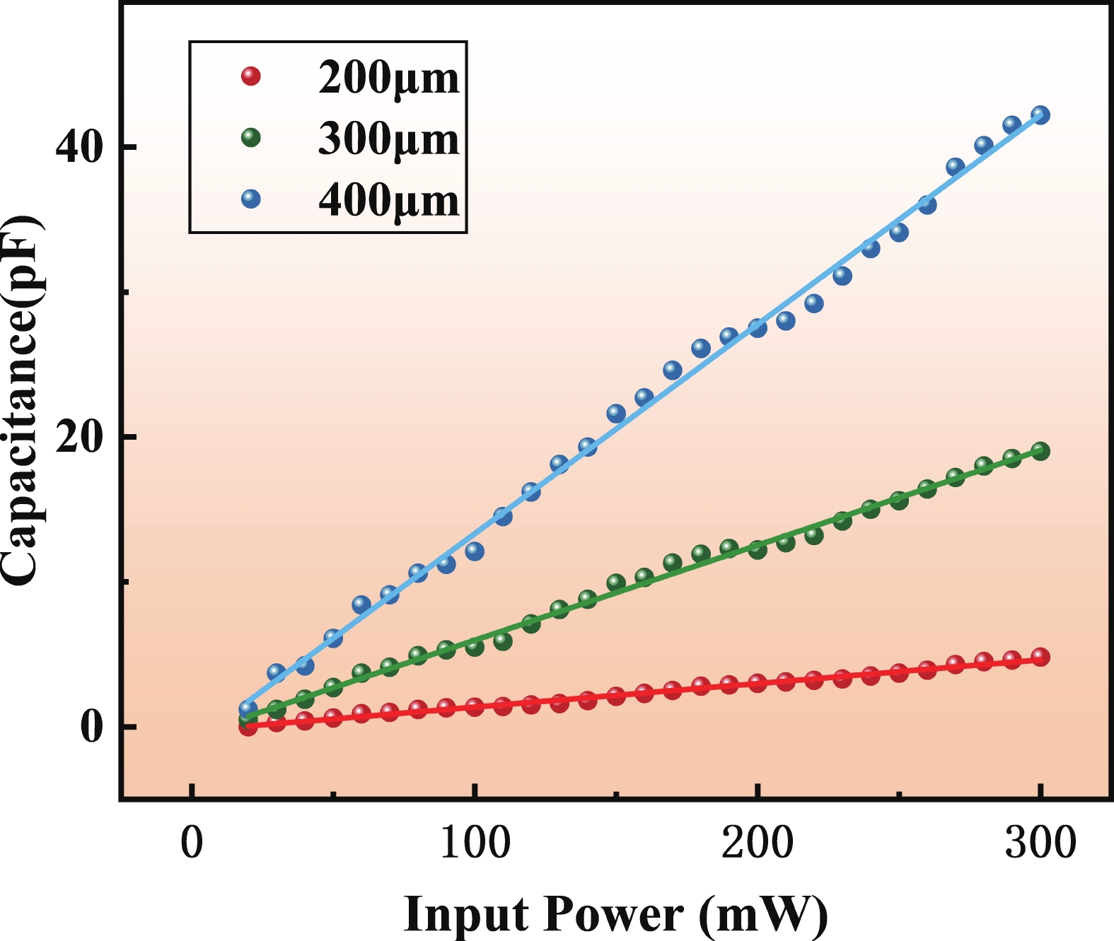
To improve the theoretical prediction accuracy of static mechanical quantities in MEMS cantilever beams for microwave power detection chips, a distributed static model is proposed based on the deflection equation. An analytical framework is established through the precise characterization of cantilever beam bending. The framework can accurately extract key electromechanical parameters, and the correlation between these parameters and geometric changes is systematically studied. Results show that the pull-in voltage increases with the gap but decreases with the length. The predicted pull-in voltage indicates a relative error of only 6.5% between the distributed static model and the simulation, which is significantly lower than that of the other two models. The overload power and sensitivity are also analyzed to facilitate performance trade-offs in chip design. The measured return loss varies between −66.46 and −10.56 dB over the 8−12 GHz frequency band, exhibiting a characteristic V-shaped trend. Moreover, the measured sensitivity of 66.5 fF/W closely matches the theoretical value of 69.3 fF/W, showing a relative error of 5.6%. These findings confirm that the distributed model outperforms the other two in terms of both accuracy and physical realism, thereby providing important reference for the design of microwave power detection chips.
J. Semicond.
2026, 47(3): 032303 doi: 10.1088/1674-4926/25100021
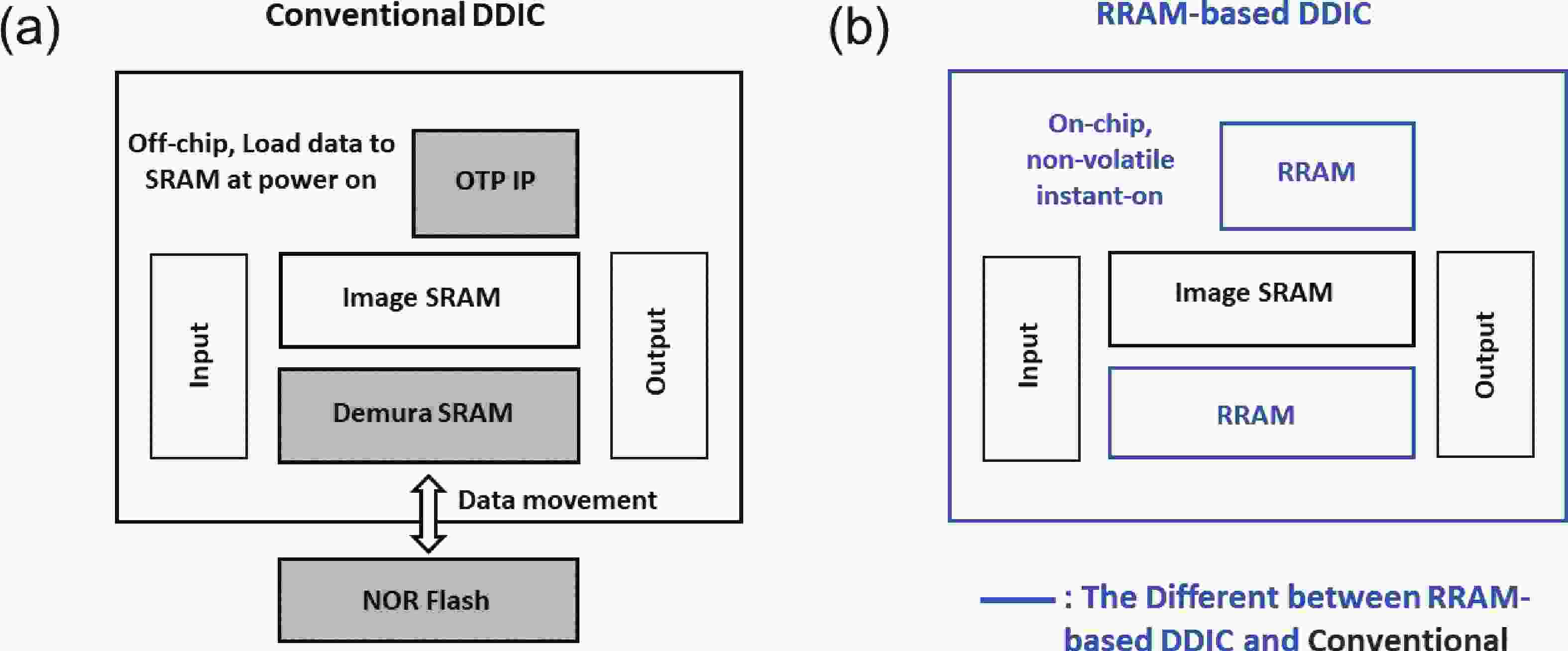
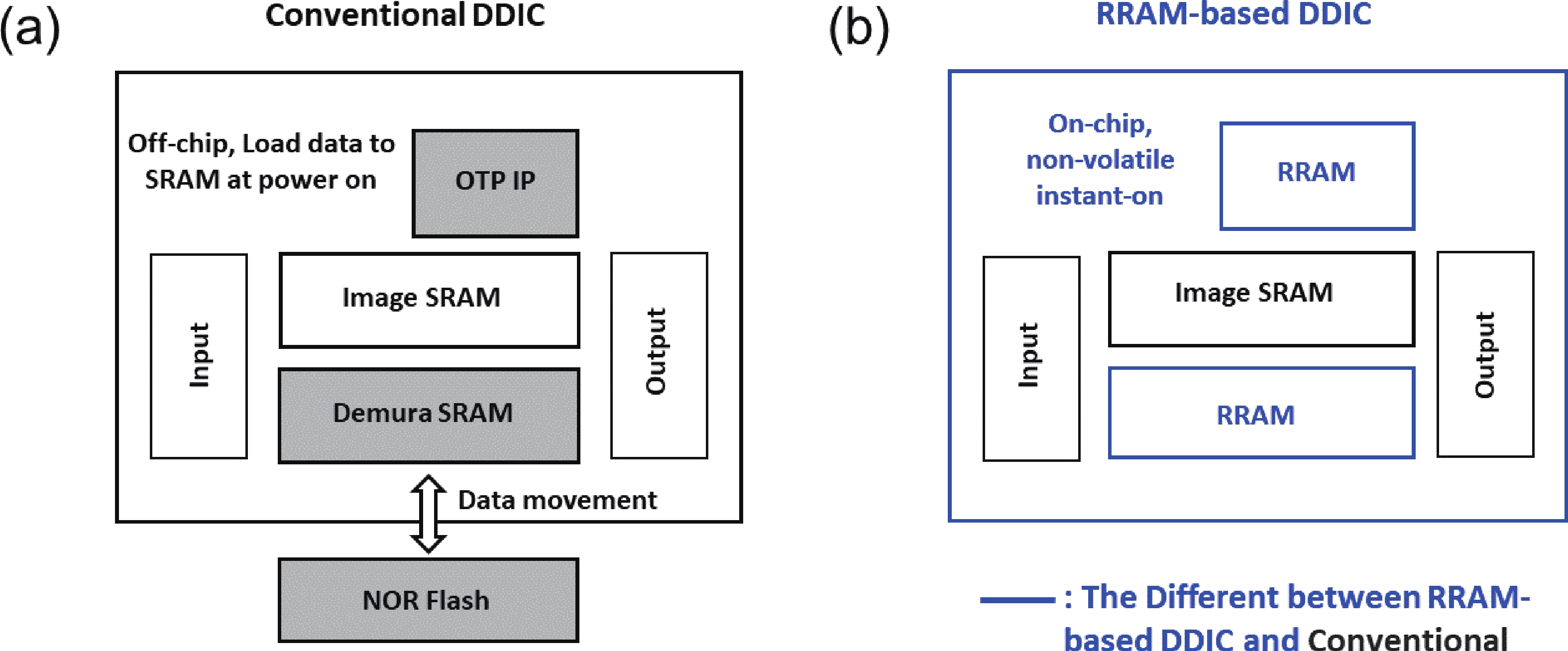
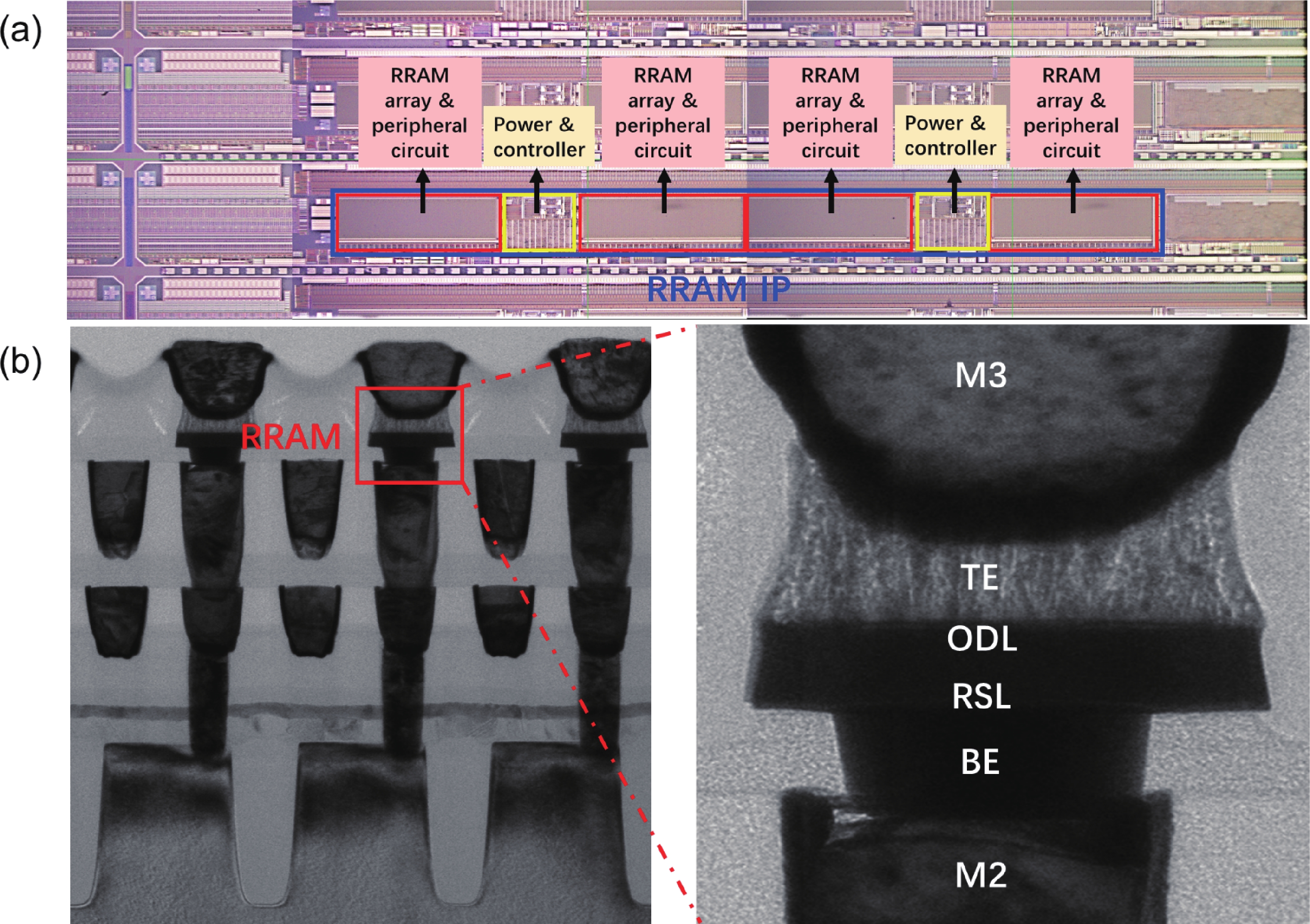
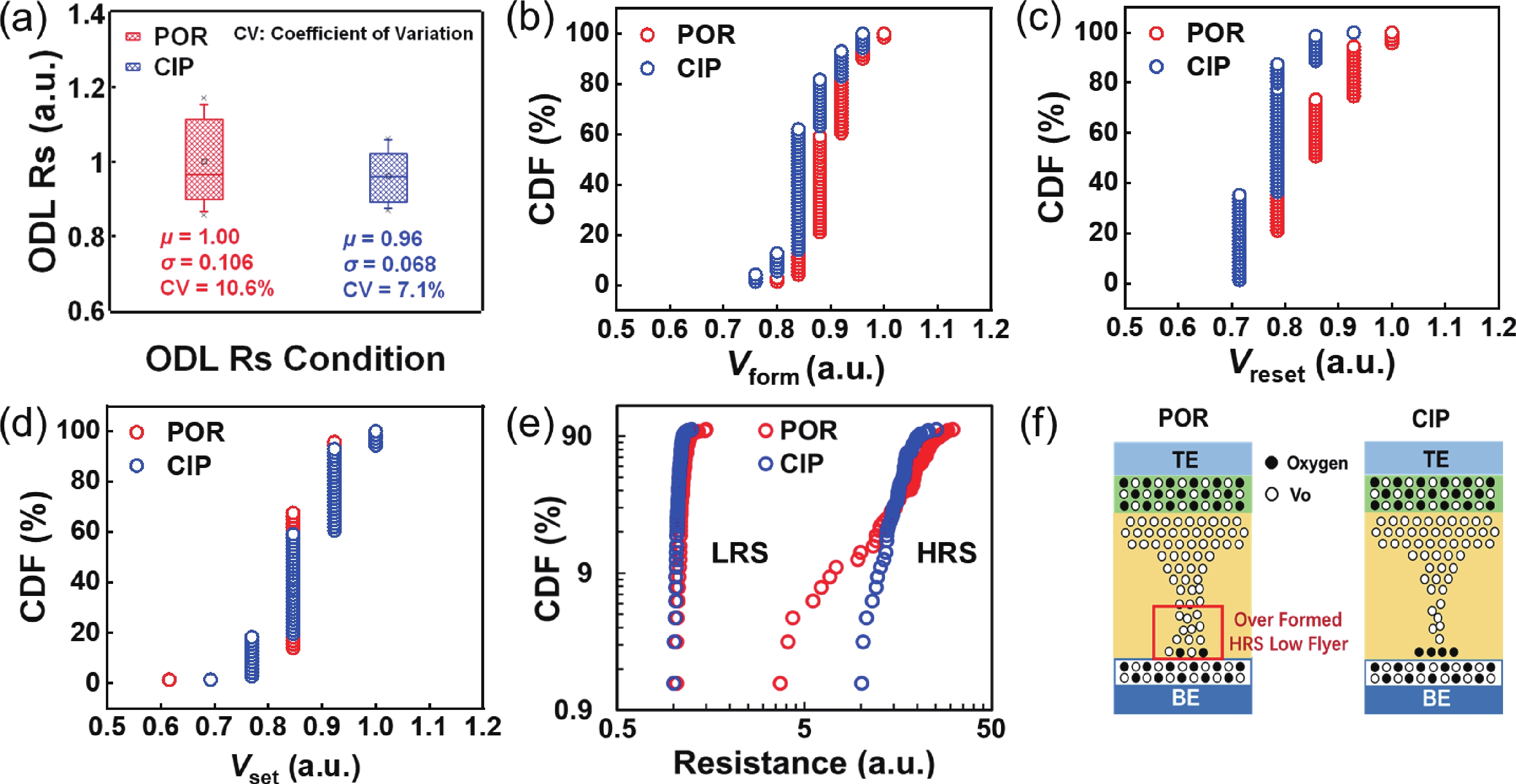
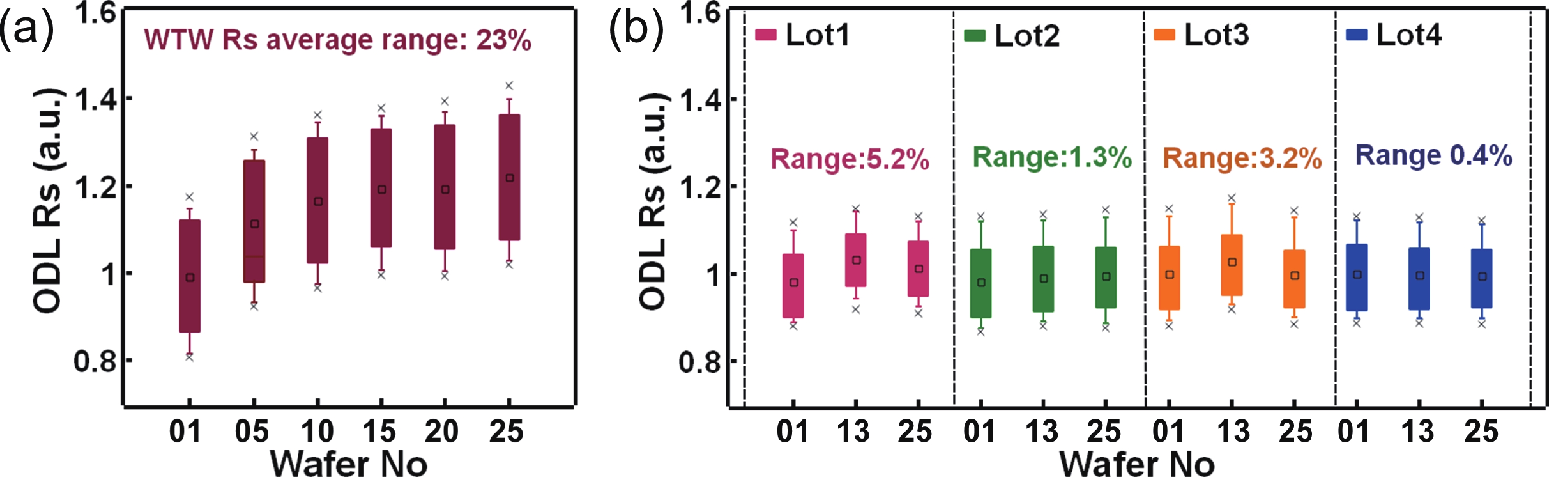
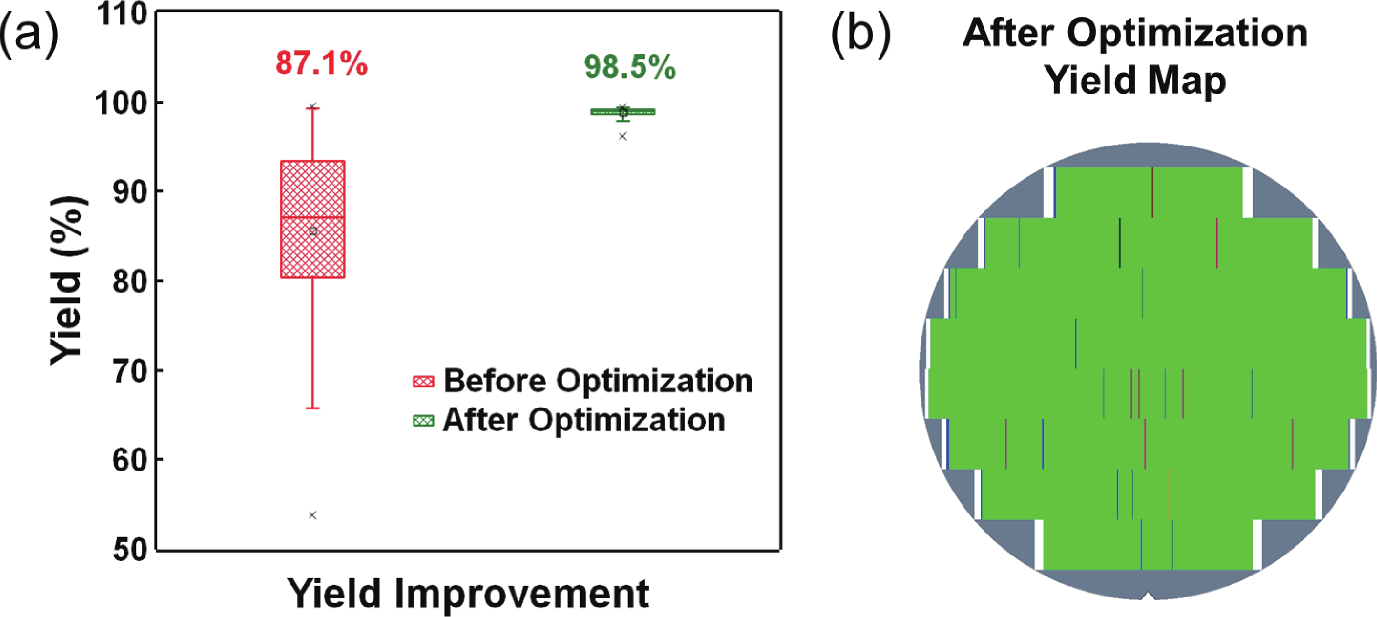
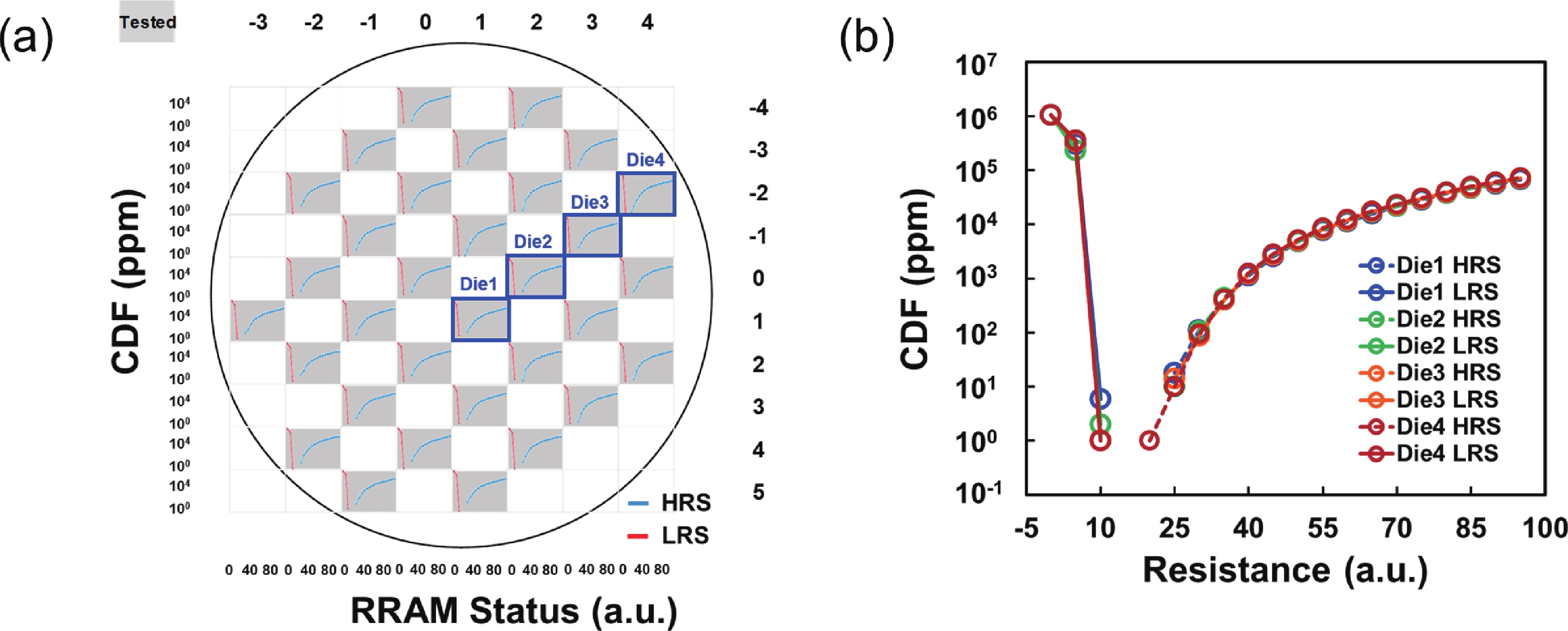
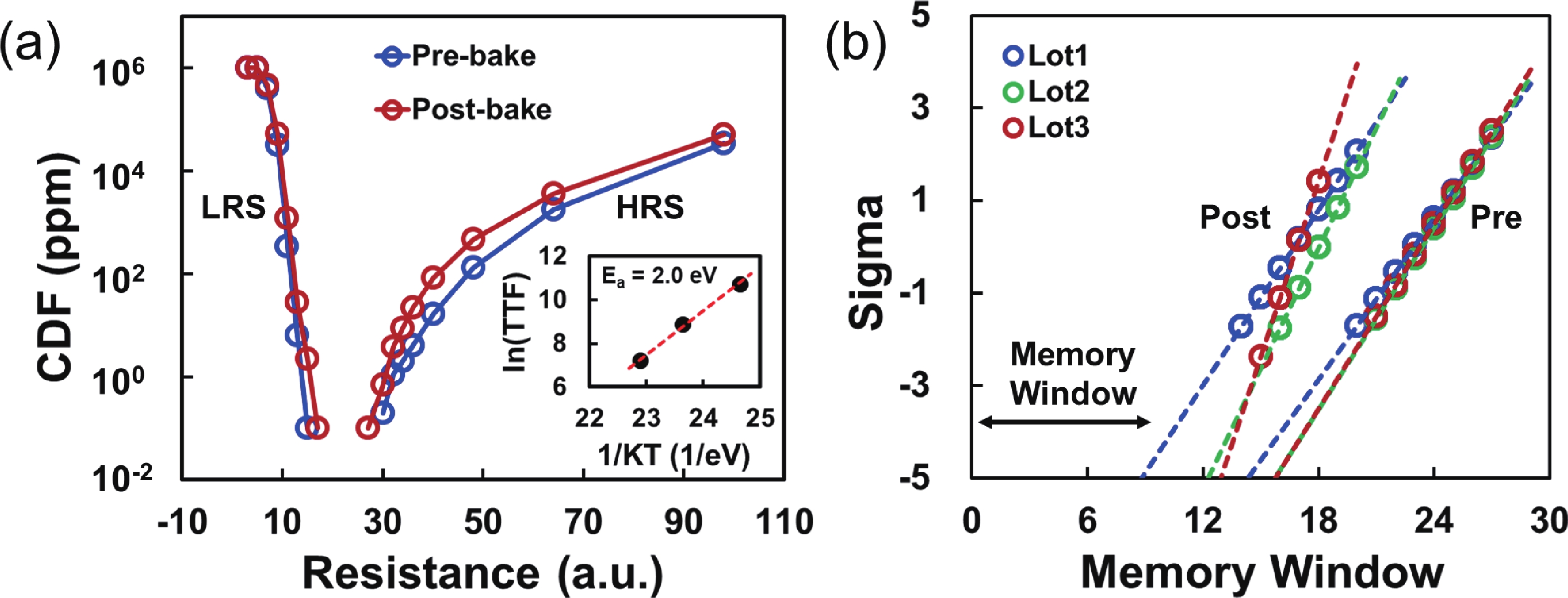
To address the challenges of complexity, power consumption, and cost constraints in traditional display driver integrated circuits (DDICs) caused by external NOR Flash and SRAM, this work proposes an embedded resistive random-access memory (RRAM) integration solution based on a 40 nm high-voltage CMOS logic platform. Targeting the yield fluctuations and stability challenges during RRAM mass production, systematic process optimizations are implemented to achieve synergistic improvements in RRAM performance and yield. Through modifications to the film sputtering and pre-deposition treatment, the within-wafer resistance uniformity (RSU) of the oxygen-deficient layer (ODL) thin film is improved from 11% to 8%, while inter-wafer process stability variation reduces from 23% to below 6%. Consequently, the yield of 8 Mb RRAM embedded mass production products increases from 87% to 98.5%. In terms of device performance, the RRAM demonstrates a fast 4.8 ns read speed, exceptional read disturb immunity of 3 × 10⁸ cycles at 95 °C, 103 write/erase endurance cycles for the 1 Mb cells, and data retention of 12.5 years at 125 °C. Post high-temperature operating life (HTOL) testing exhibits stable high/low resistance window. This study provides process optimization strategies and a reliability assurance framework for the mass production of highly integrated, low-power embedded RRAM display driver IC.
J. Semicond.
2026, 47(3): 032304 doi: 10.1088/1674-4926/25060021
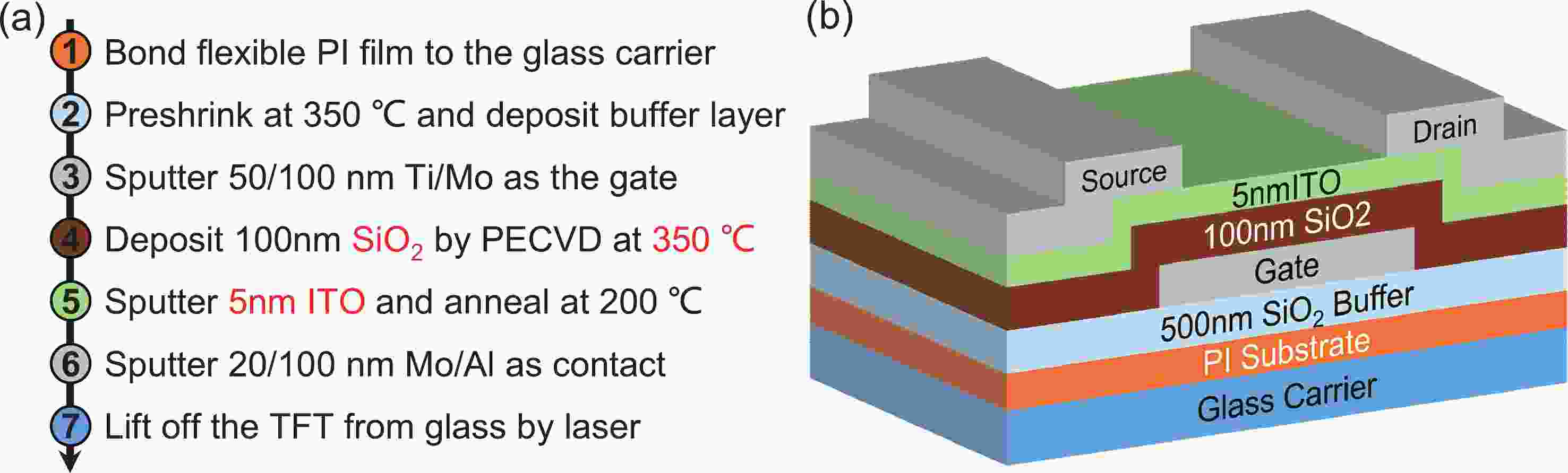
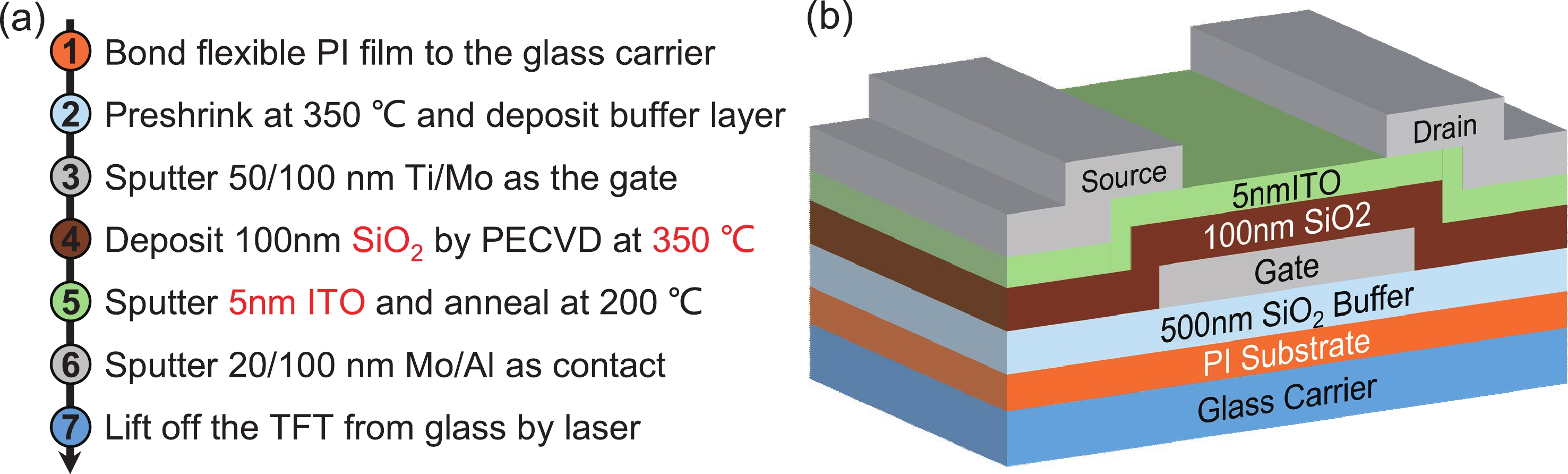
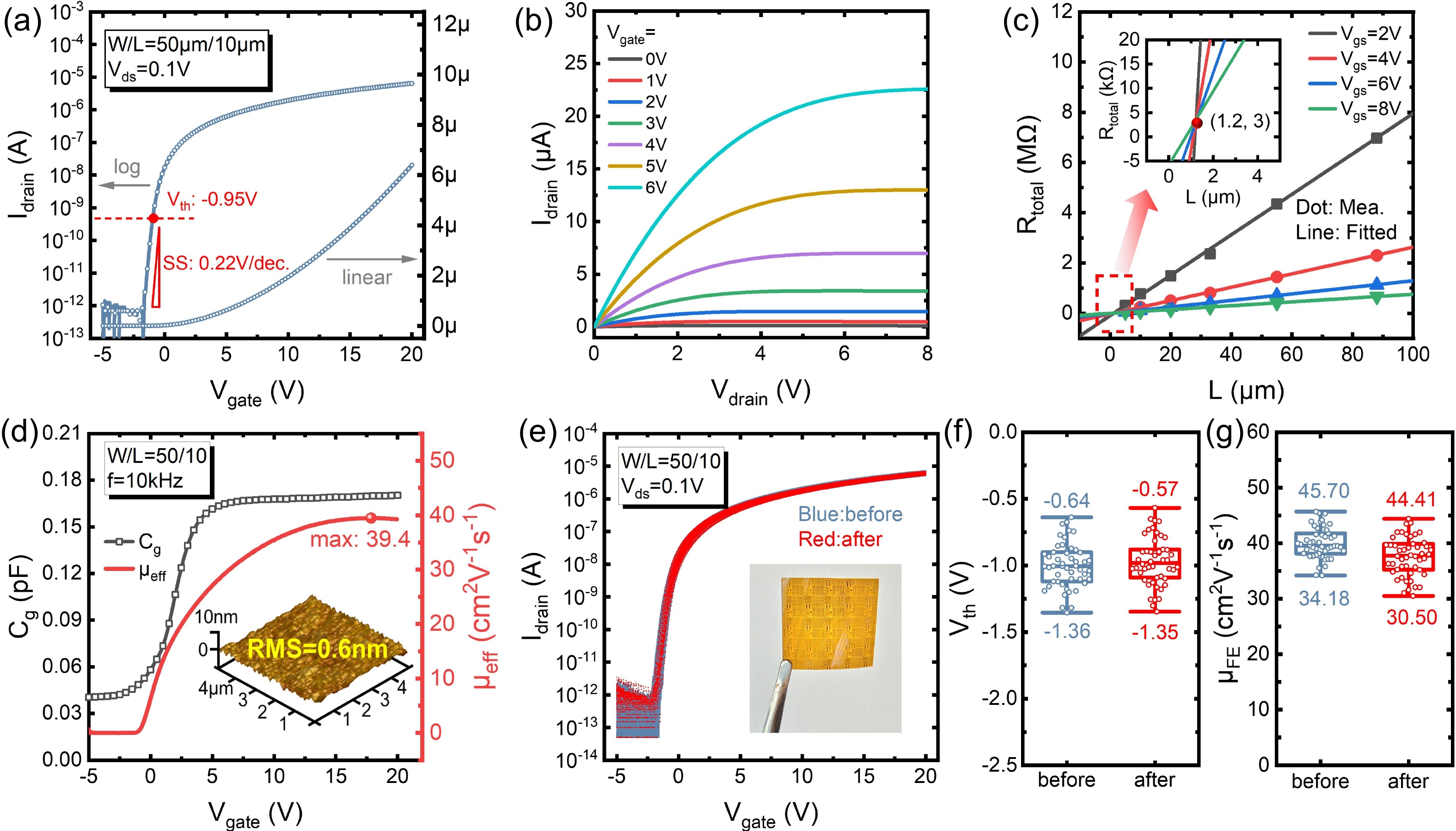
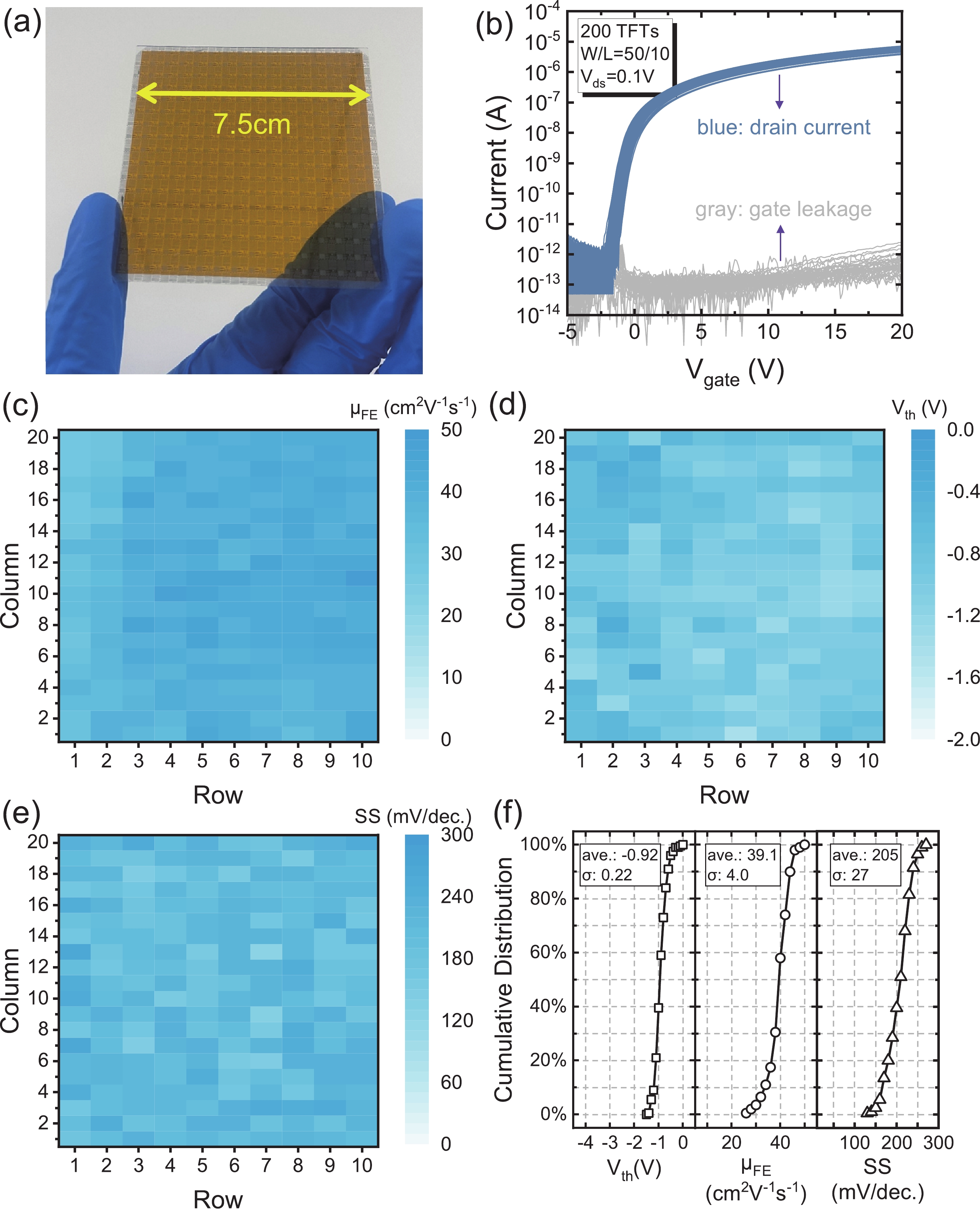
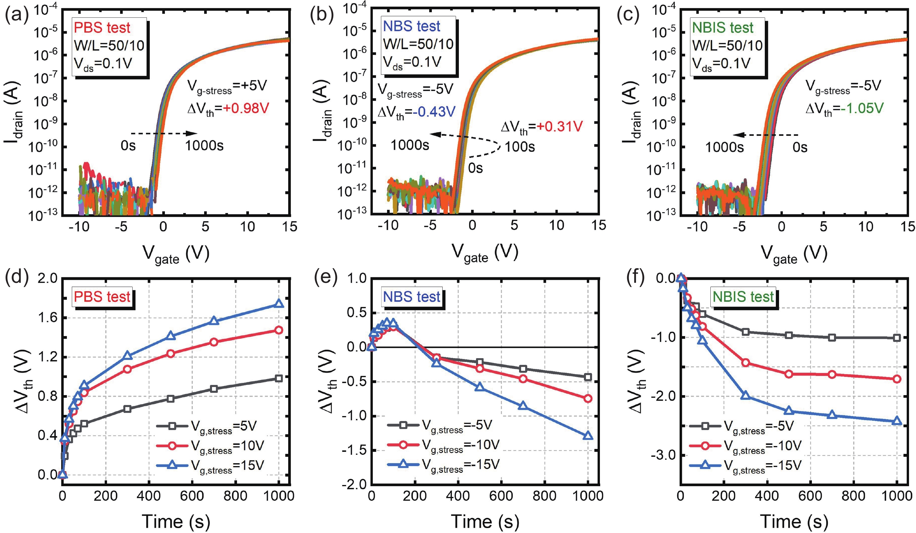
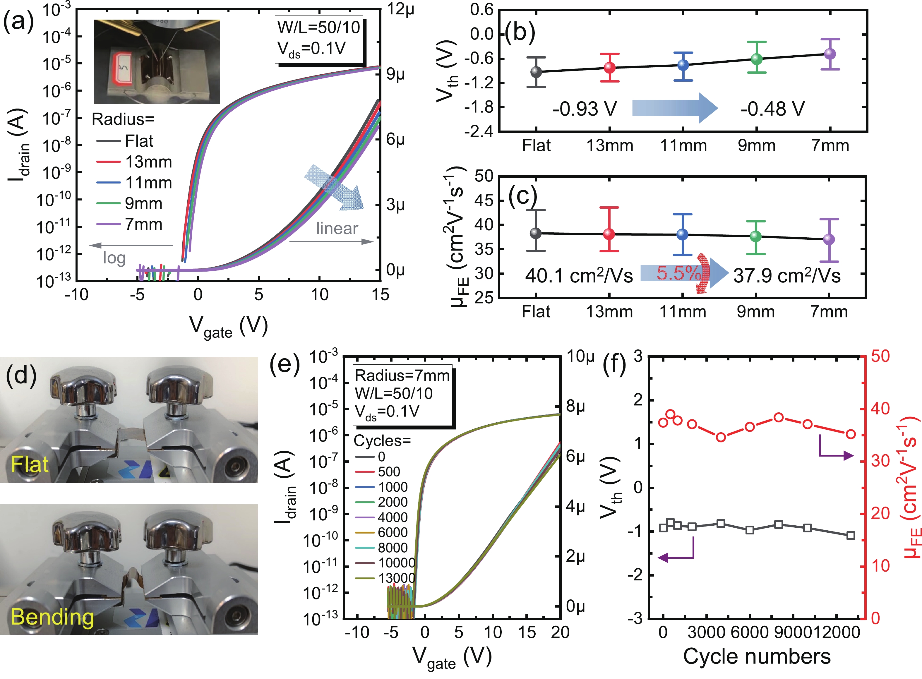
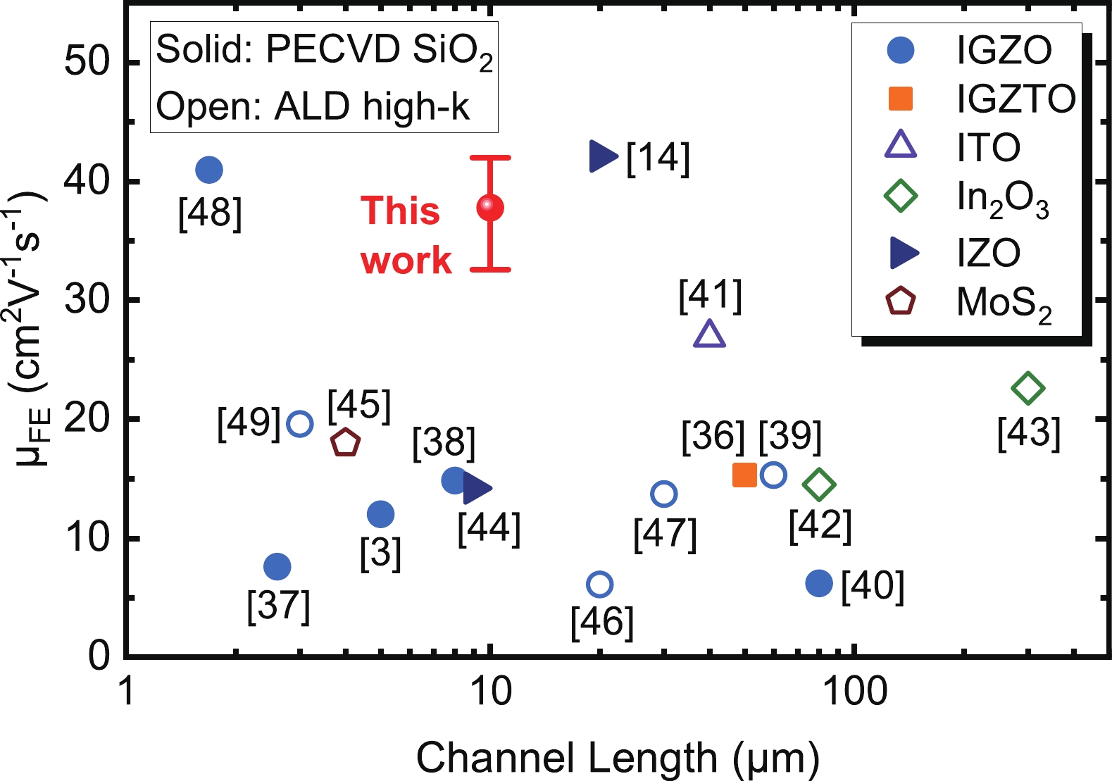
The increasing pursuit of ultra-high resolution displays has driven the demand for thin film transistors (TFTs) with higher mobility, especially on flexible substrates. In this work, we developed indium tin oxide (ITO) TFTs on flexible substrates for the first time and achieved a remarkable average mobility of 39.1 cm2·V−1·s−1, via mass-production compatible processes utilizing SiO2 gate dielectric. Benefiting from the ultra-flat surface and extremely low coefficient of thermal expansion (CTE) of our PI substrate, the ITO TFTs exhibit excellent large-scale uniformity. Additionally, the TFTs generate minor variations of −5.5% and +0.45 V in mobility and threshold voltage under a bending radius of 7 mm, respectively. They stay fully functional even after a dynamic bending test up to 13 000 cycles, observing no obvious degradation in mobility and threshold voltage. The reliable mechanical flexibility and robust bending durability demonstrate their great potential for ultra-high resolution flexible displays in the future.
J. Semicond.
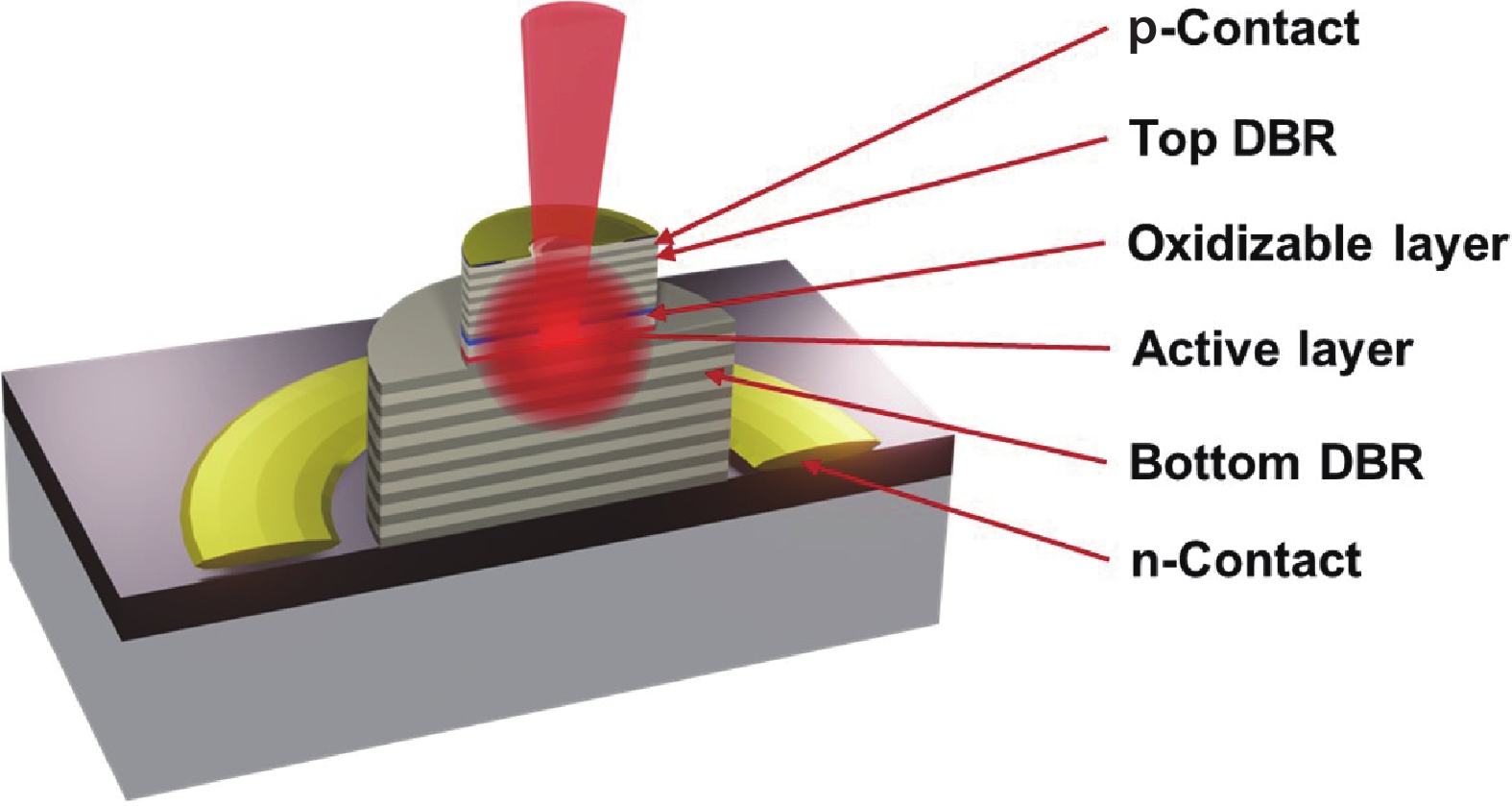
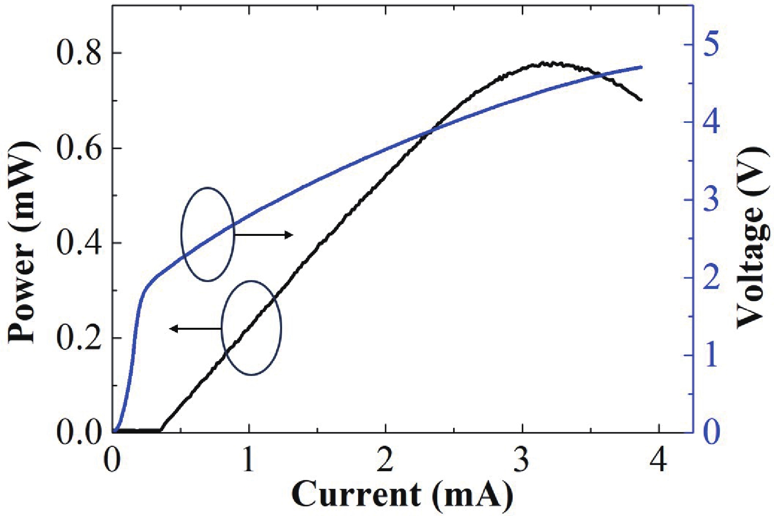
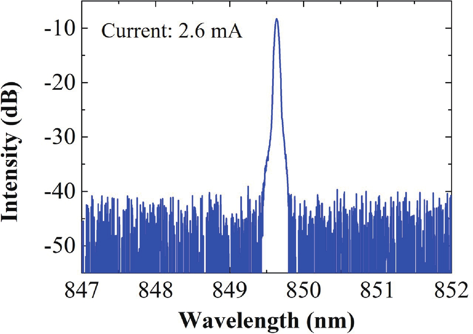
2026, 47(3): 032401 doi: 10.1088/1674-4926/25090008
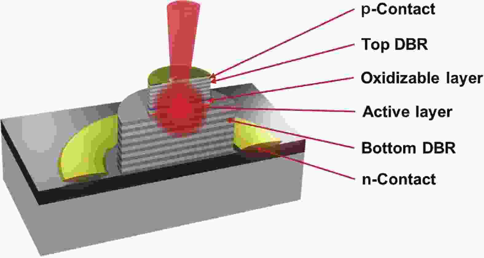
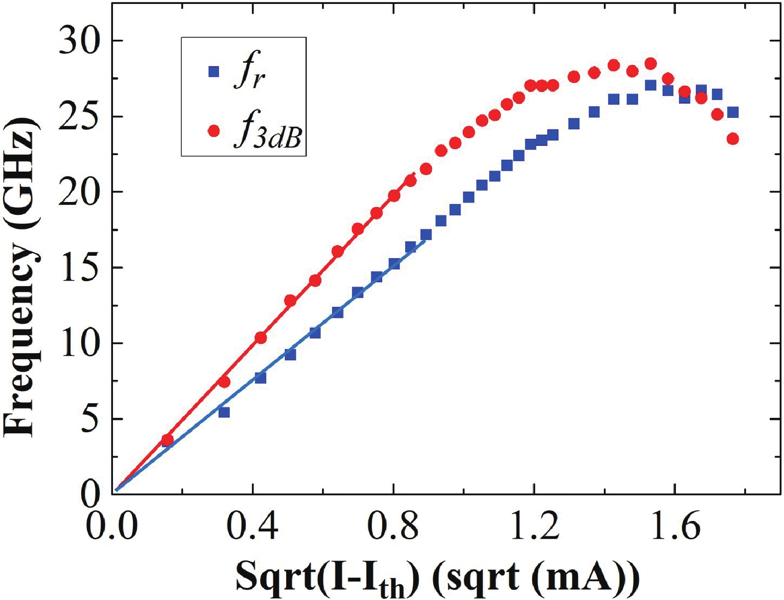
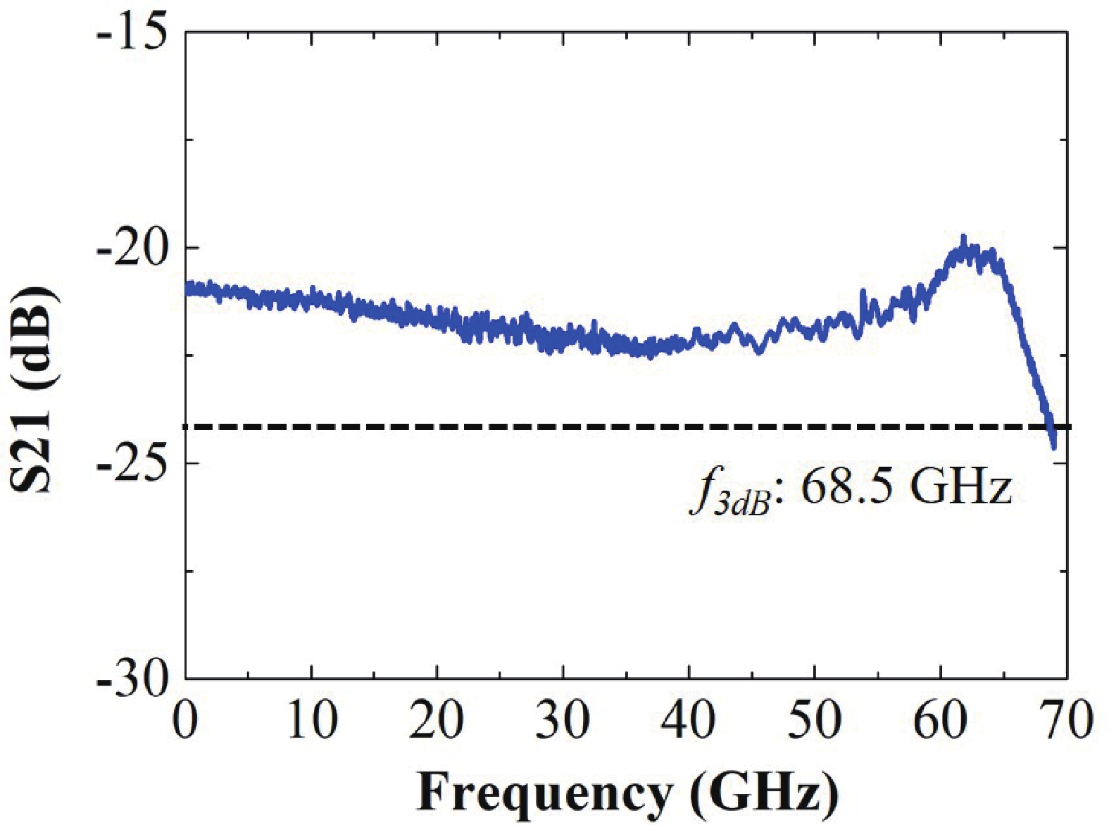
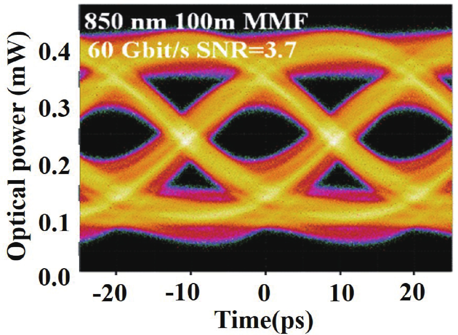
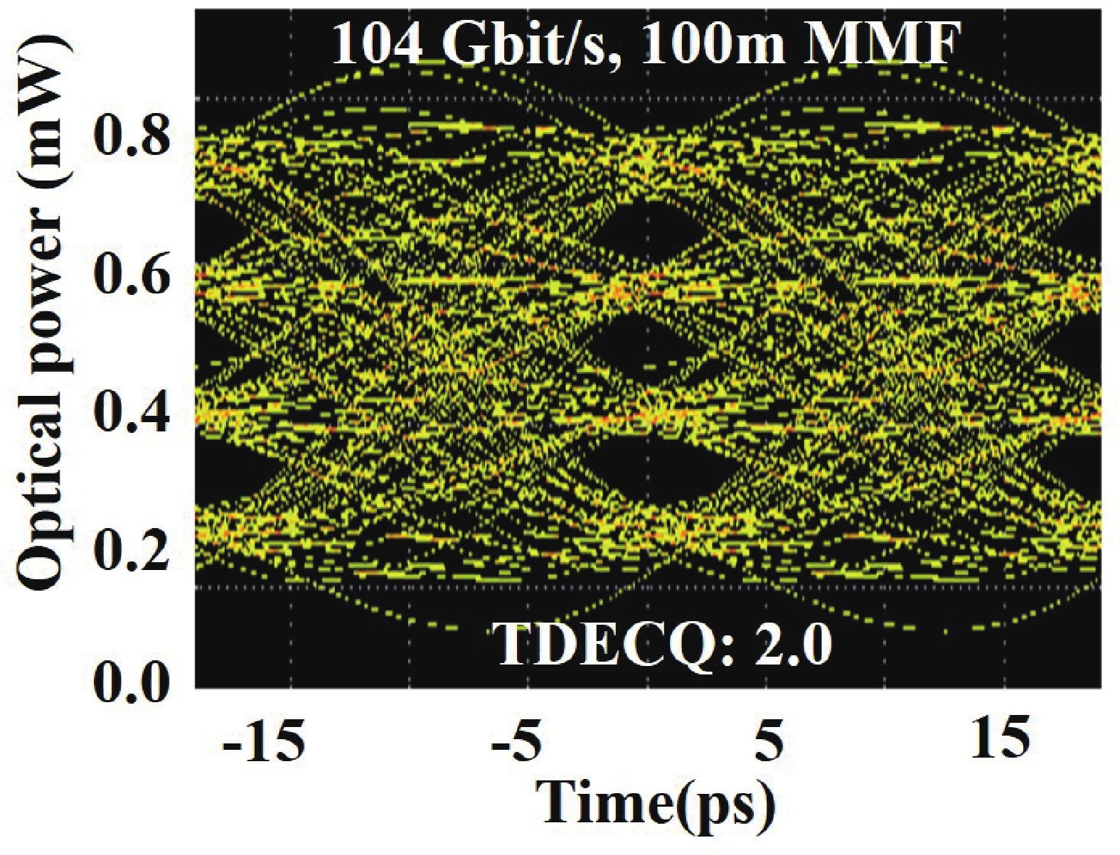
A high-speed single-mode vertical-cavity surface-emitting laser (VCSEL) is one of the most important light sources for optical interconnects in data centers. Single-mode VCSEL can improve the transmission distance. In this letter, we demonstrate a single-mode 850 nm VCSEL with a bit rate of 60 Gb/s under NRZ modulation and 104 Gb/s under PAM4 modulation across a 100 m length of OM5 fiber, without the need for equalization or a filter. In addition, by using optical injection locking, the 3 dB bandwidth is enhanced to 68.5 GHz.
J. Semicond.
2026, 47(3): 032402 doi: 10.1088/1674-4926/25080023
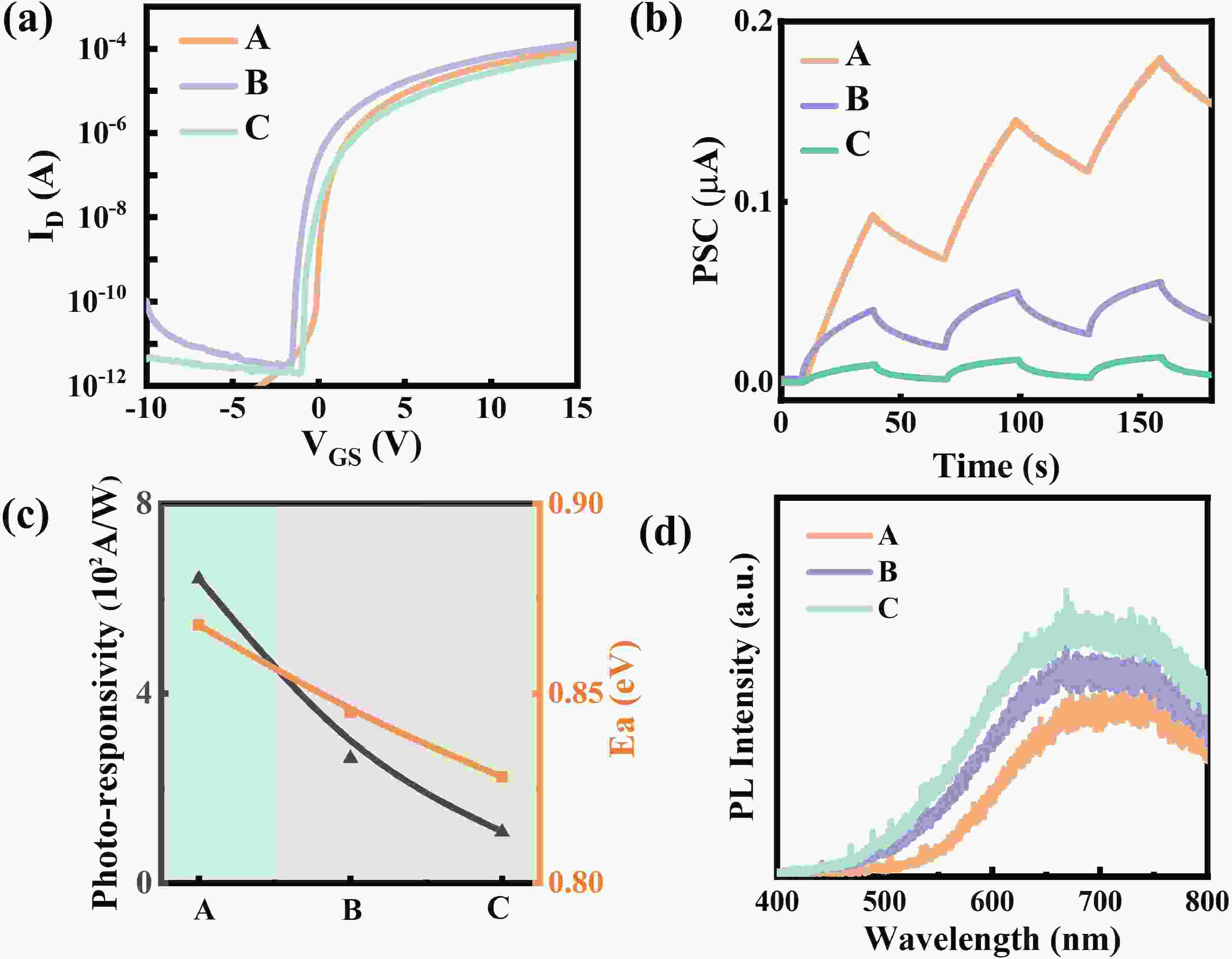
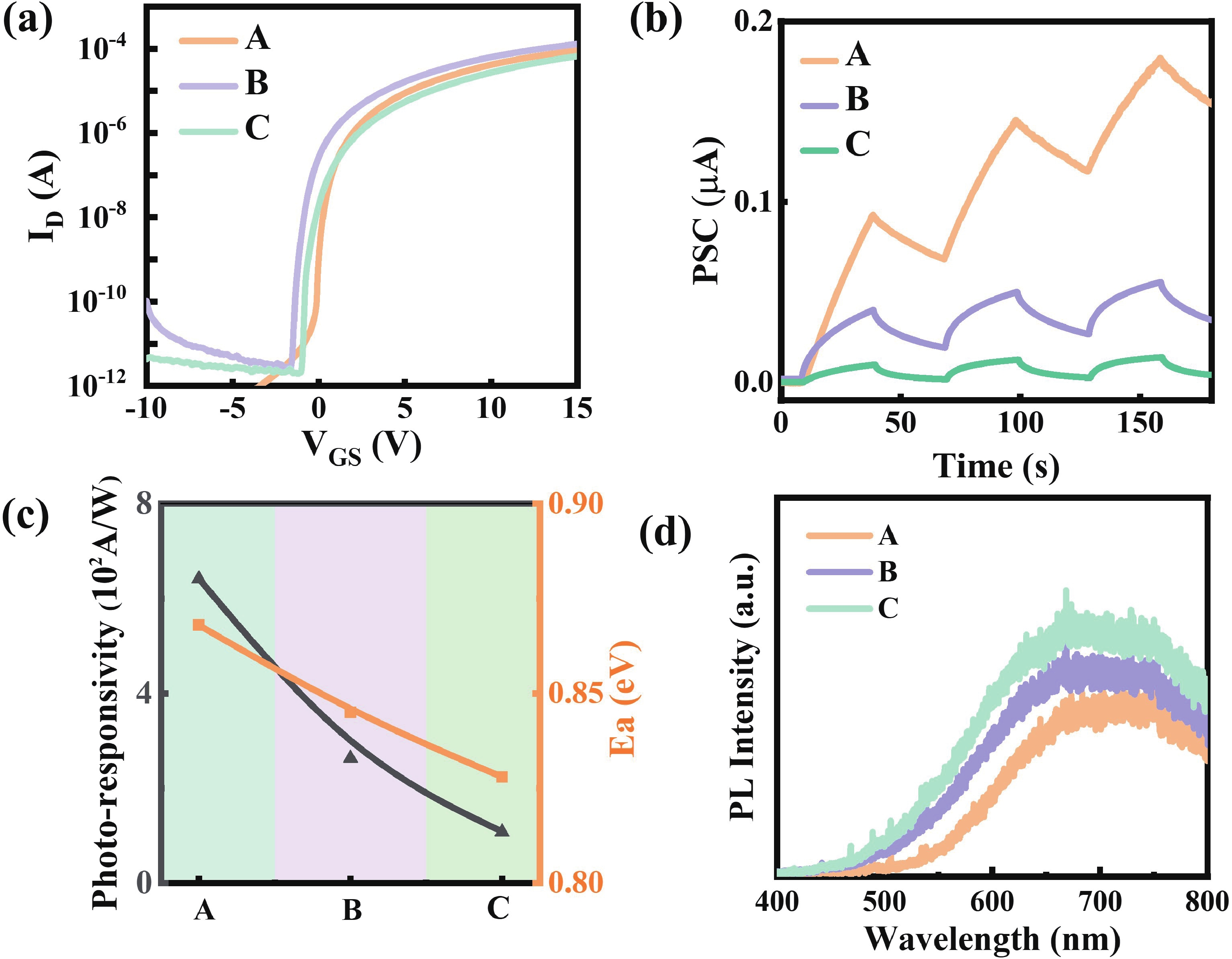
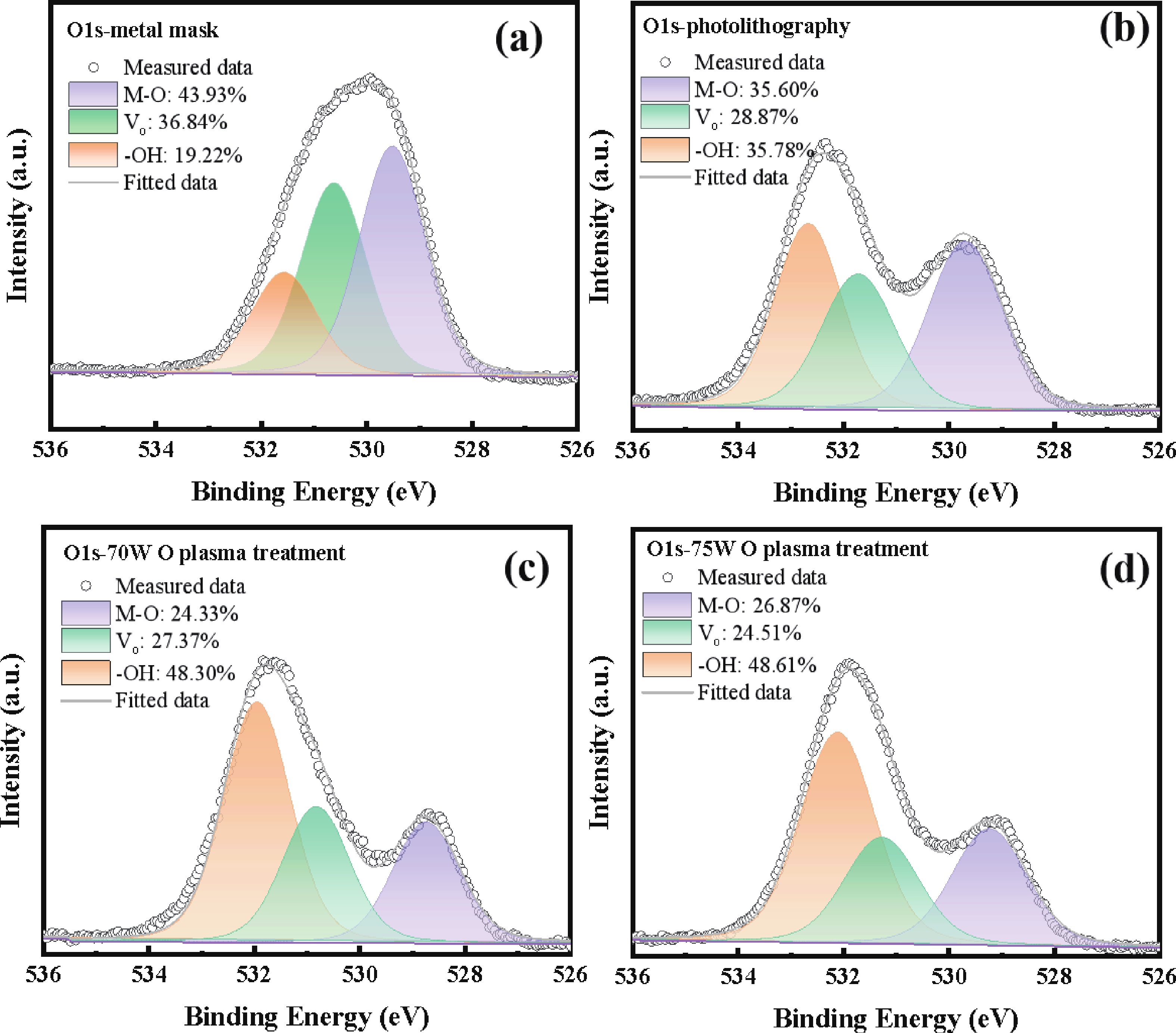
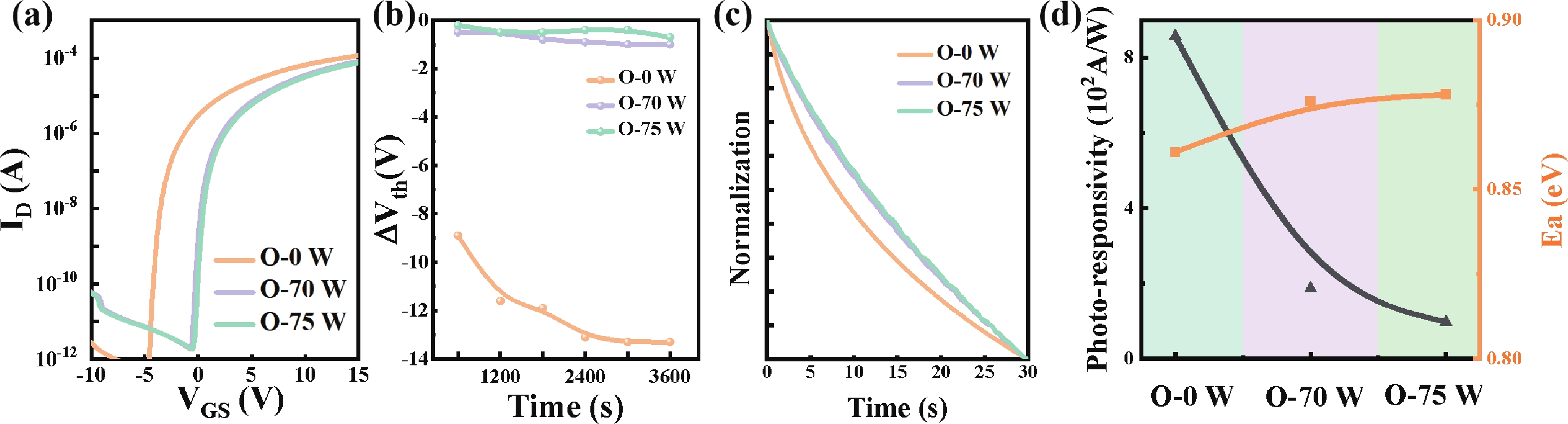
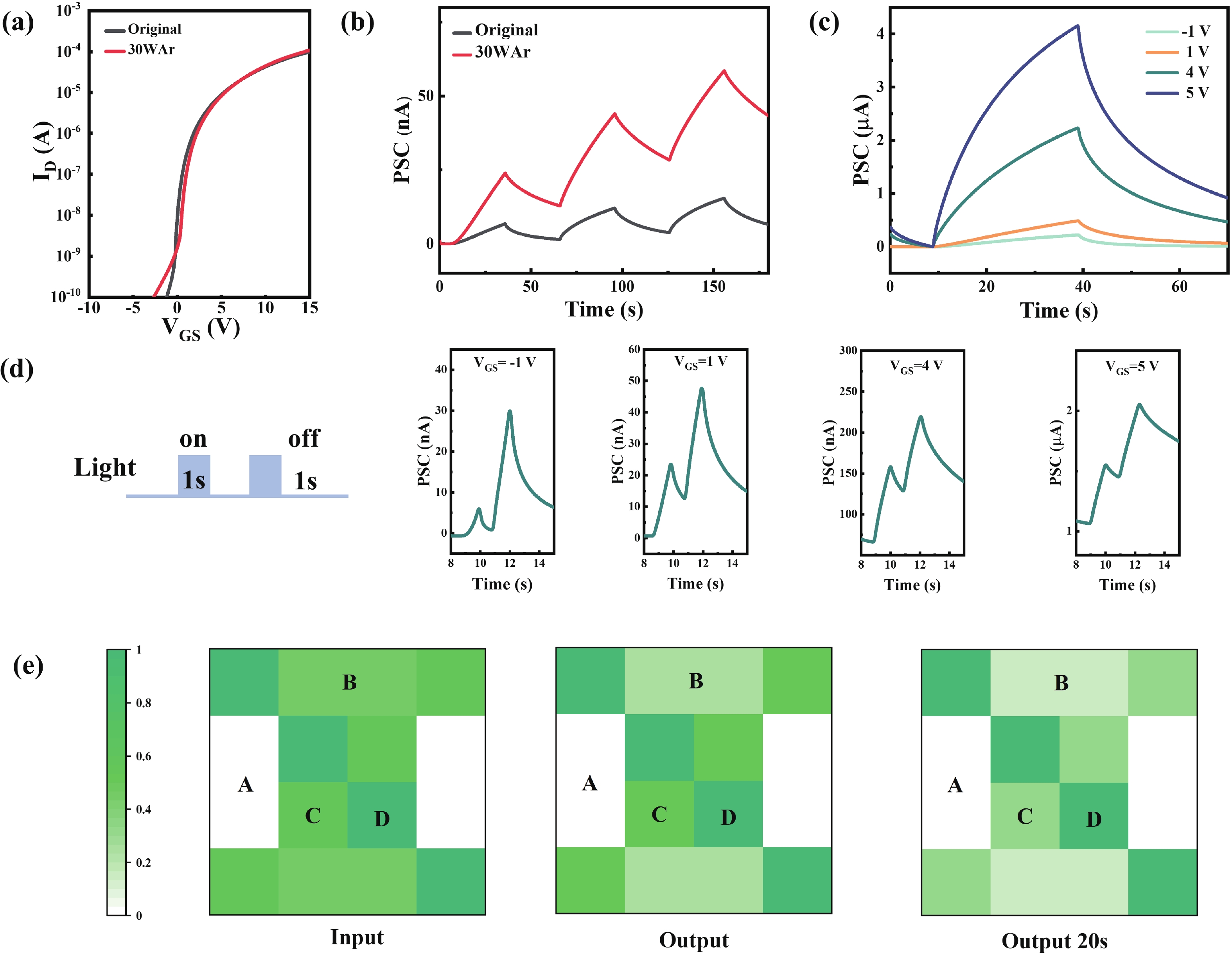
Oxide semiconductor-based neuromorphic devices hold great potential for visual information processing, yet their performance is critically limited by photolithography-induced organic residues. This work systematically investigates the effects of photoresist contaminants on In−Ga−Zn−O thin-film transistors (IGZO TFTs), revealing that these residues introduce deep-level trap states that degrade both photo-responsivity and carrier transport dynamics. Through optimized plasma-assisted surface treatments, these adverse effects would be effectively eliminated. Additionally, we show that gate−voltage modulation can precisely control the relaxation kinetics of photocarriers in these devices. By applying these strategies to IGZO-based synaptic arrays, we achieve enhanced image contrast through controlled optoelectronic response modulation. Overall, our findings highlight the critical impact of photolithography-induced organic residues in IGZO optoelectronic synaptic devices and demonstrate an effective approach for performance enhancement through surface plasma treatment and gate−voltage modulation.
J. Semicond.
2026, 47(3): 032501 doi: 10.1088/1674-4926/25090026
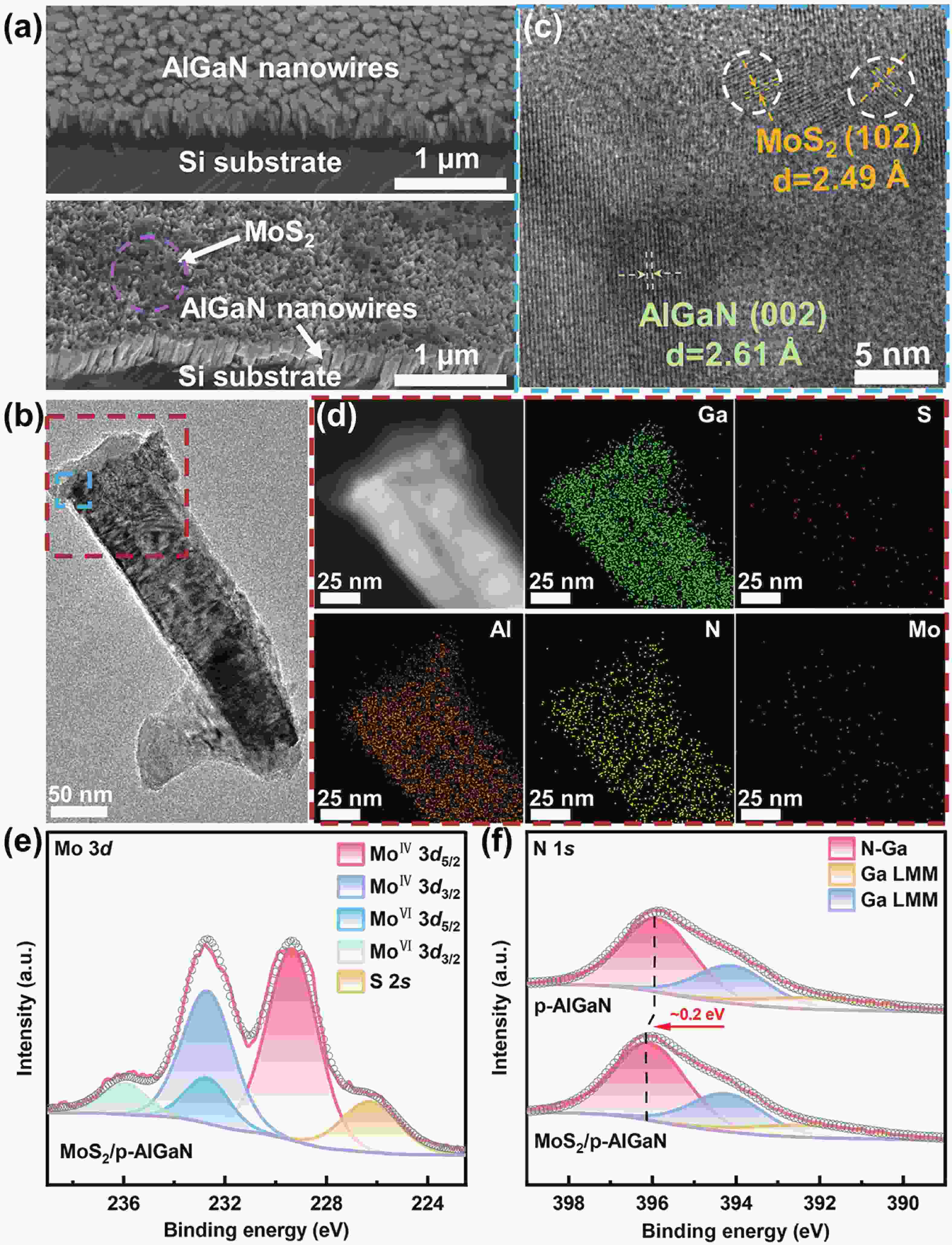
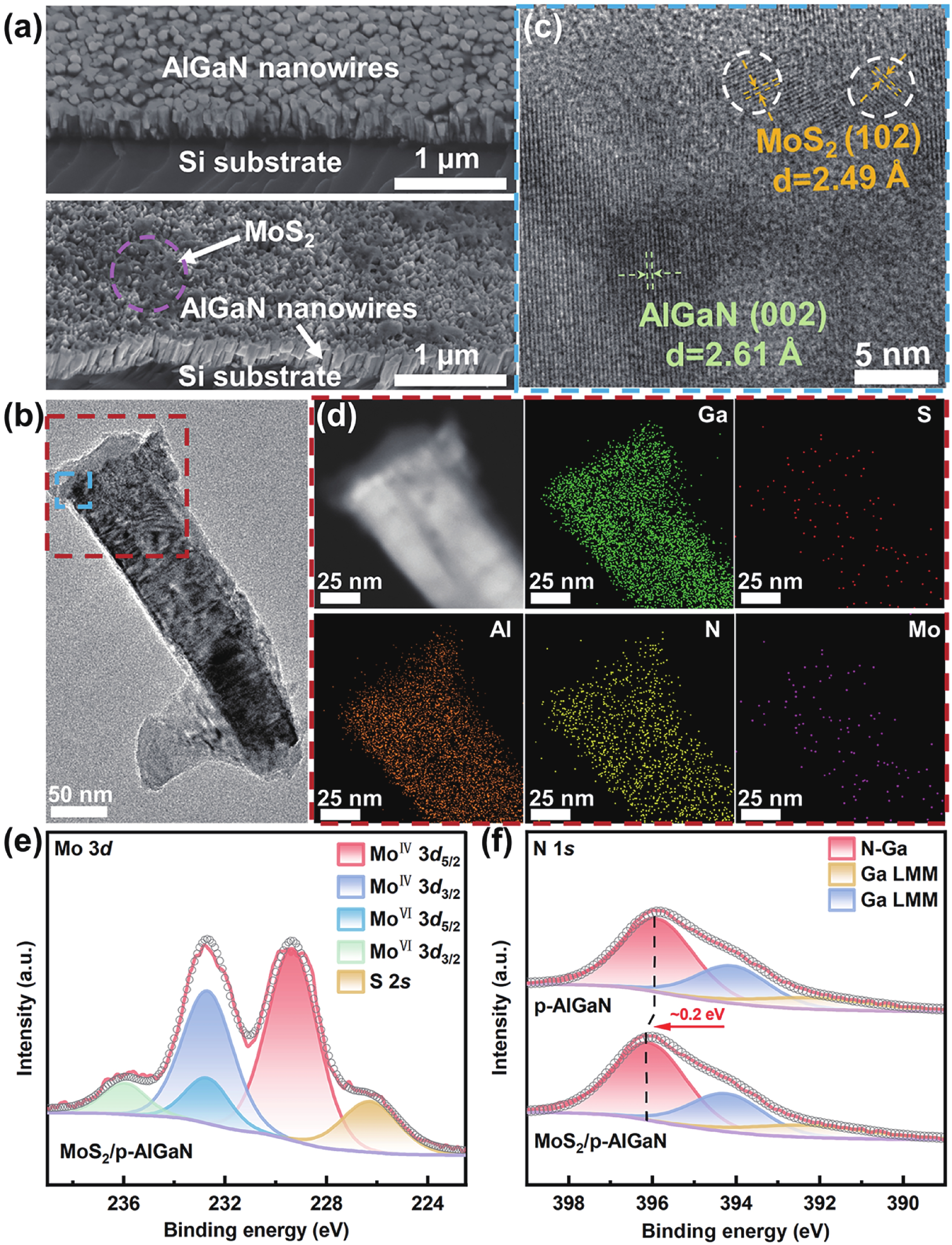
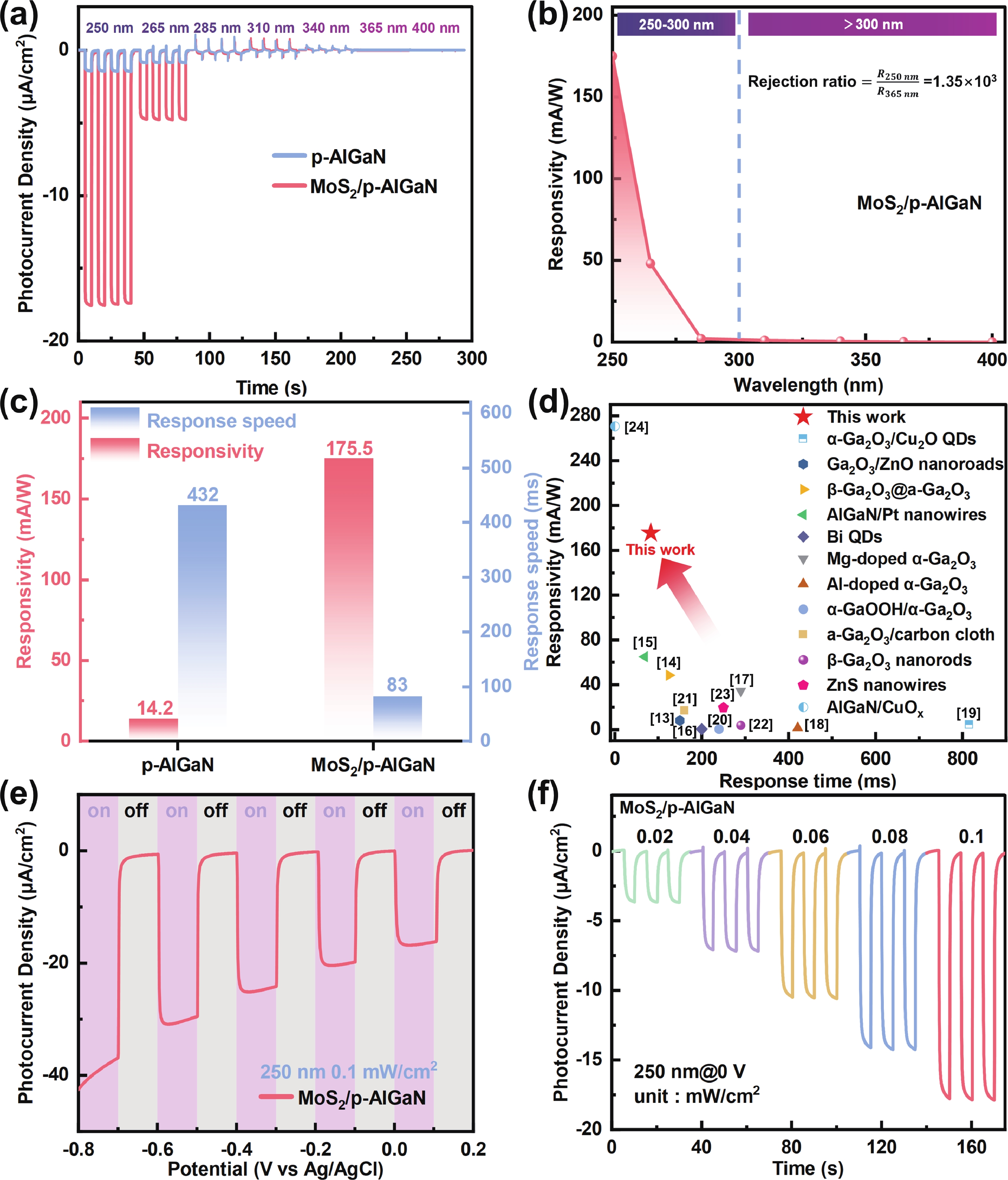
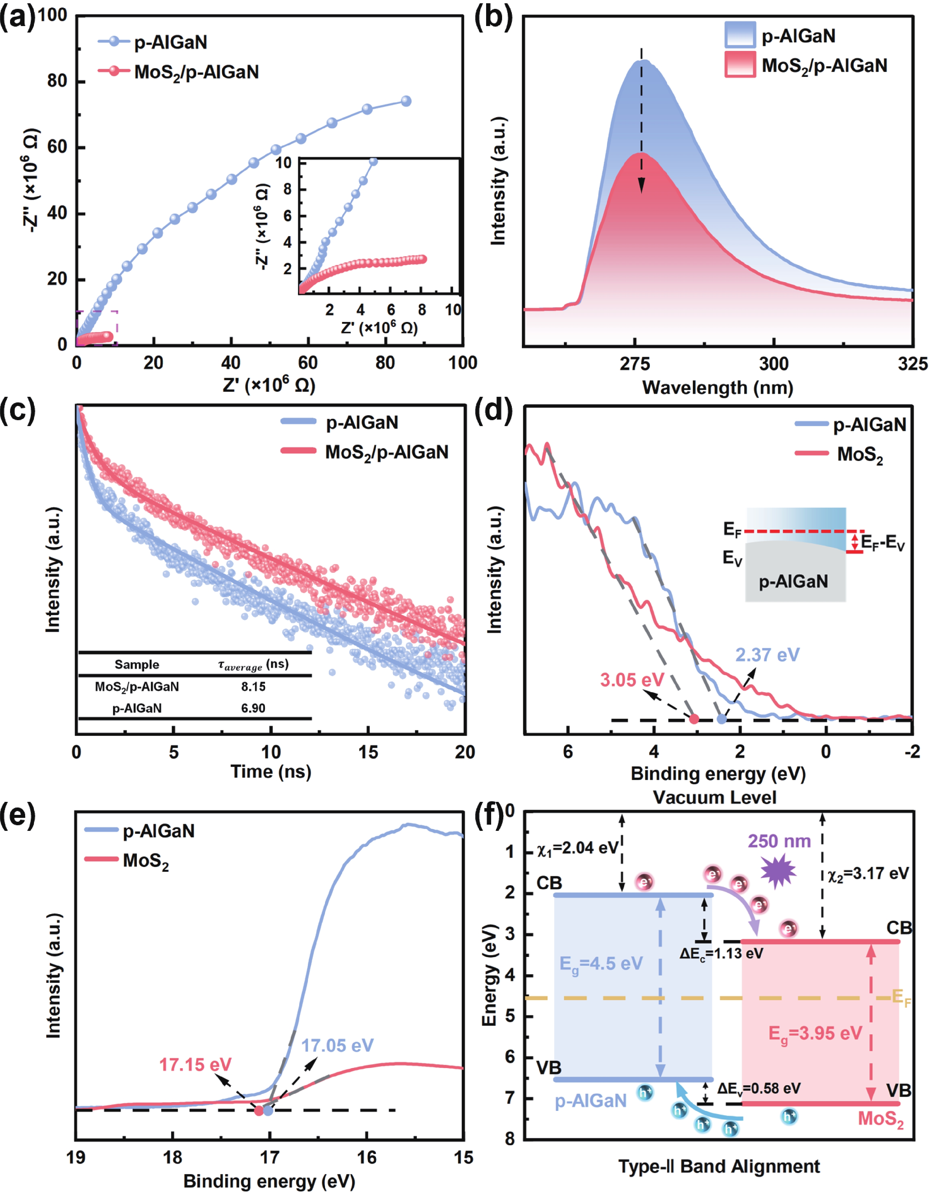
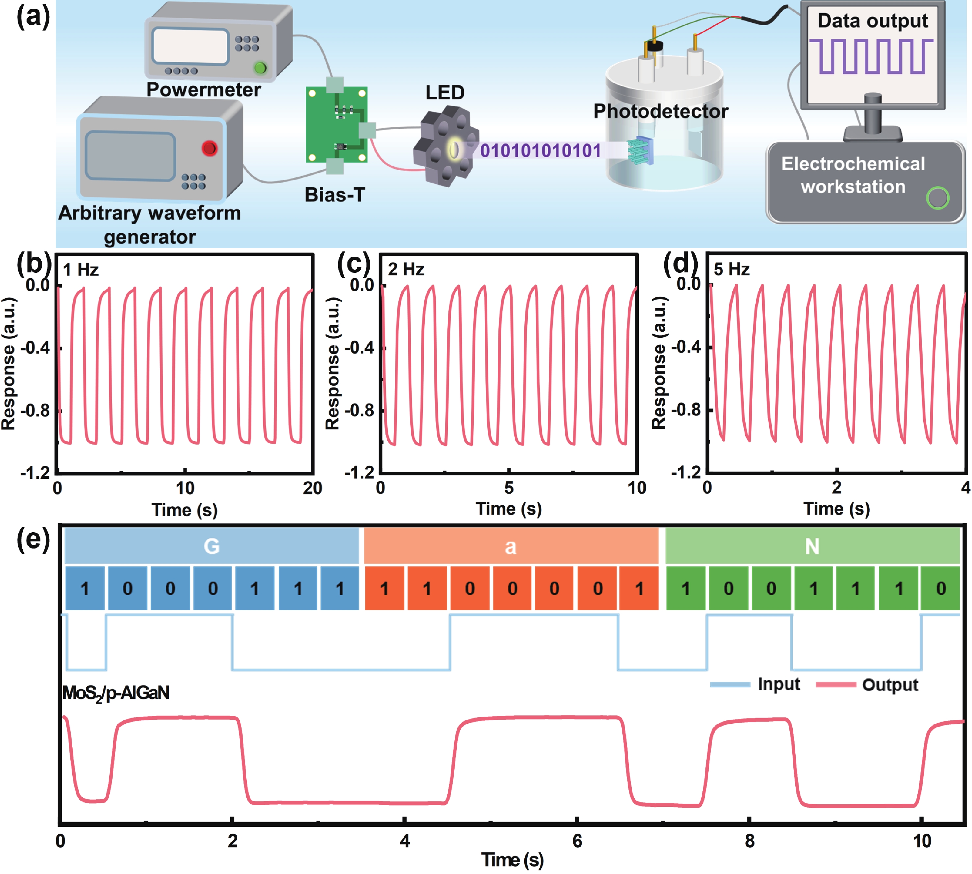
Solar-blind ultraviolet photodetectors (UV PDs), capable of detecting UV radiation without interference from sunlight, have attracted significant interest. Herein, we propose a 0D/1D heterostructure for UV PDs, which was fabricated by spin-coating MoS2 quantum dots onto p-AlGaN nanowires. The device achieves a high responsivity of 175.5 mA/W and a fast response speed of 83 ms at 250 nm illumination under self-powered mode, which improved nearly 1235% and 521% after MoS2 decoration, respectively. These improvements can be attributed to the type-Ⅱ heterostructure formed between p-AlGaN and MoS2, which facilitates enhanced charge separation and carrier transport. Later, we demonstrate the implementation of this device in optical communication, achieving high-accuracy transmission of "GaN" ASCII code signals. Such a 0D/1D heterostructure provides an effective strategy for high-performance solar-blind UV PD.
J. Semicond.
2026, 47(3): 032502 doi: 10.1088/1674-4926/25050032
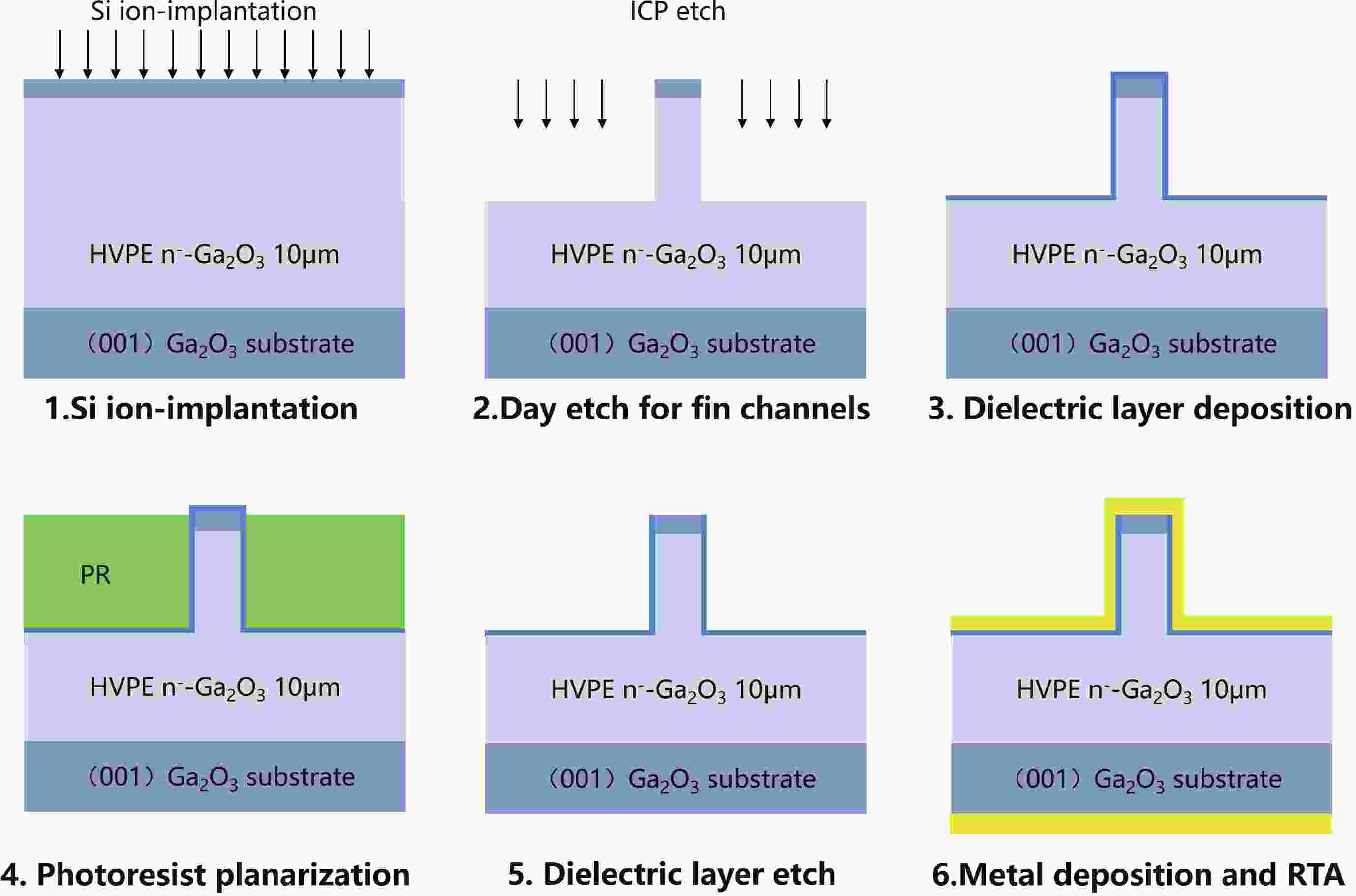
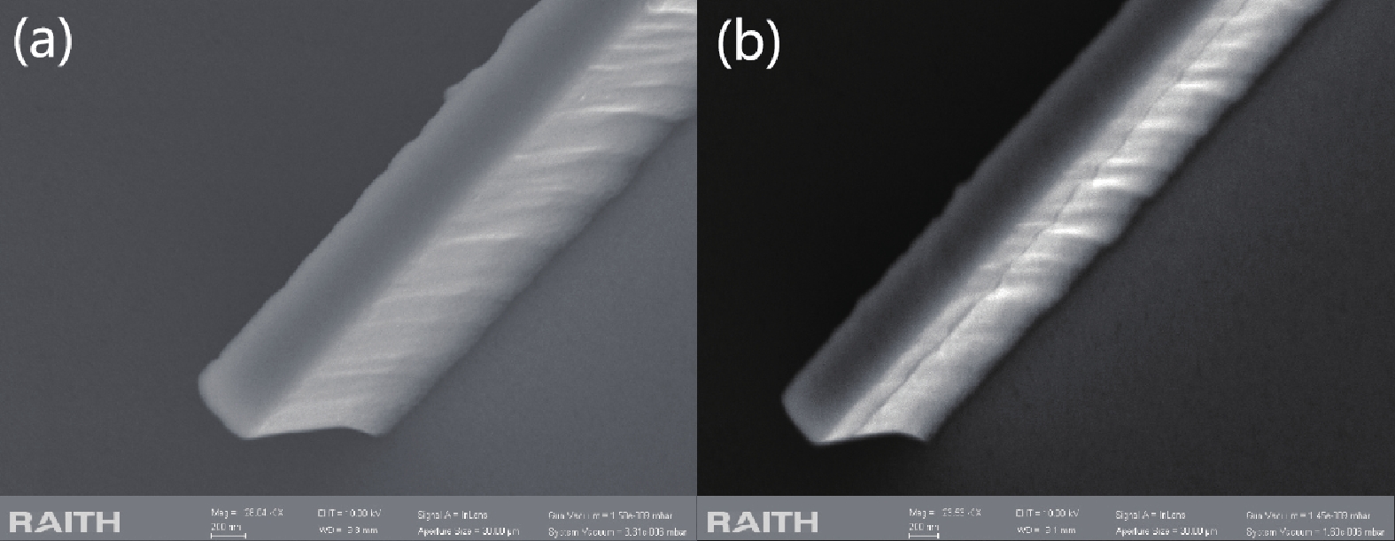
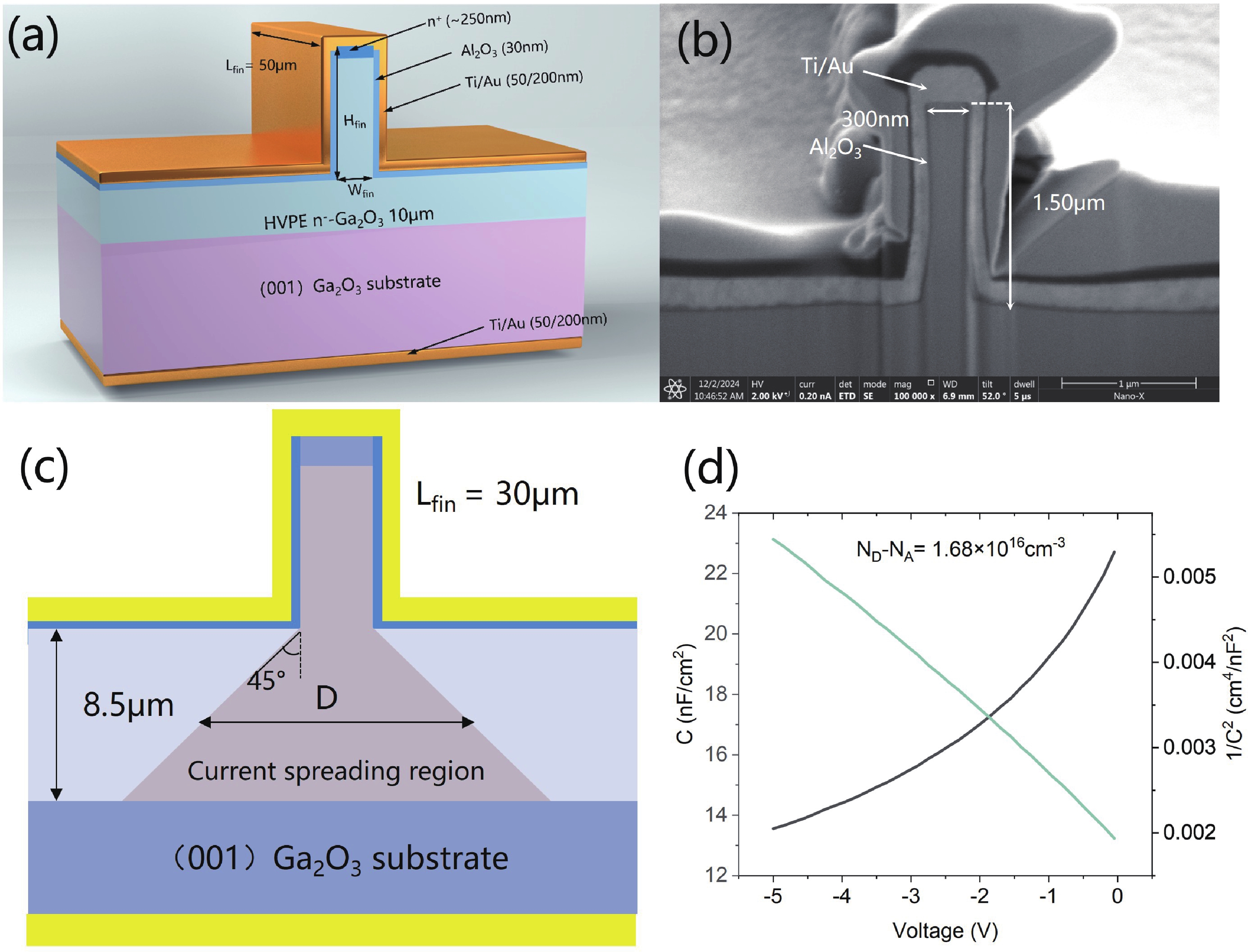
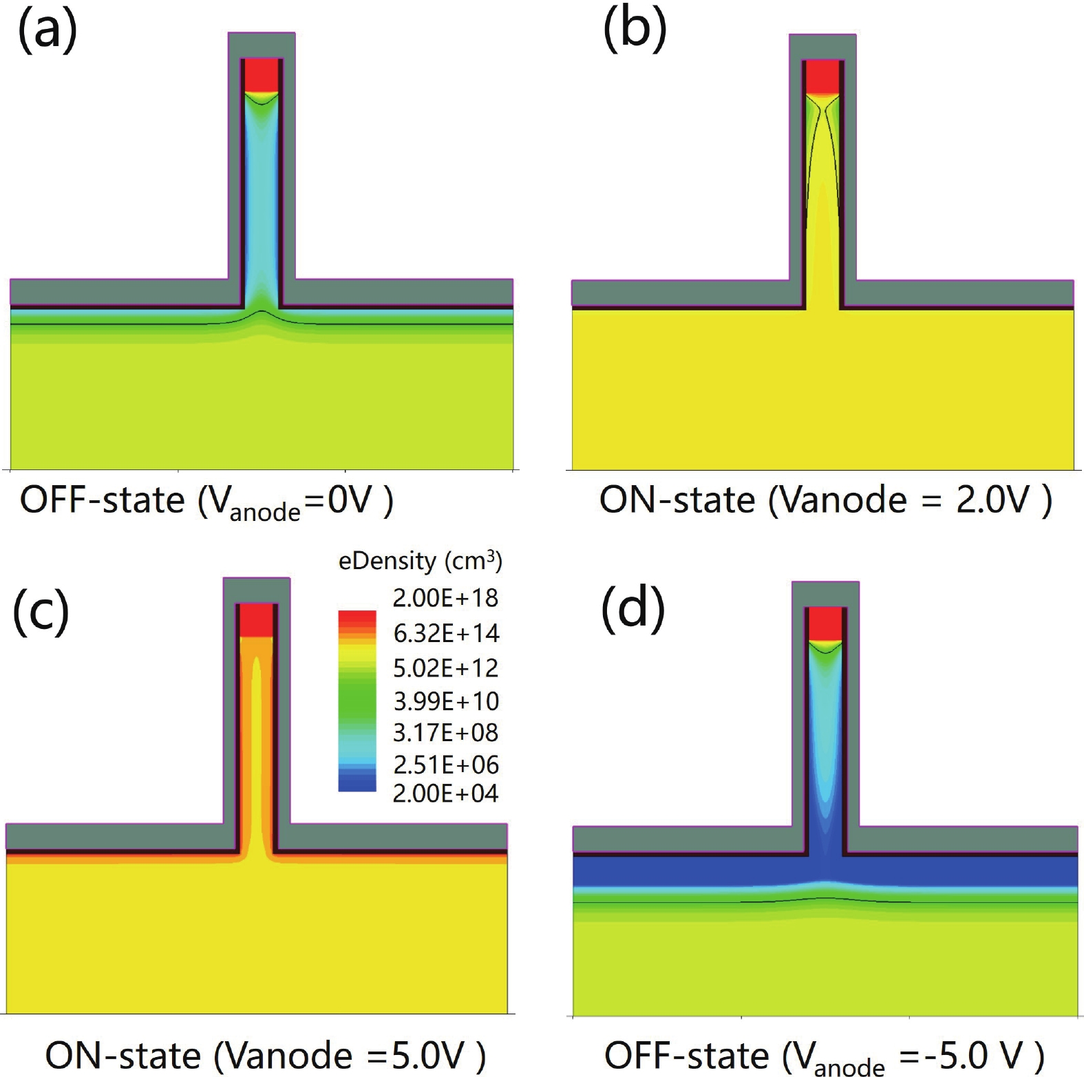
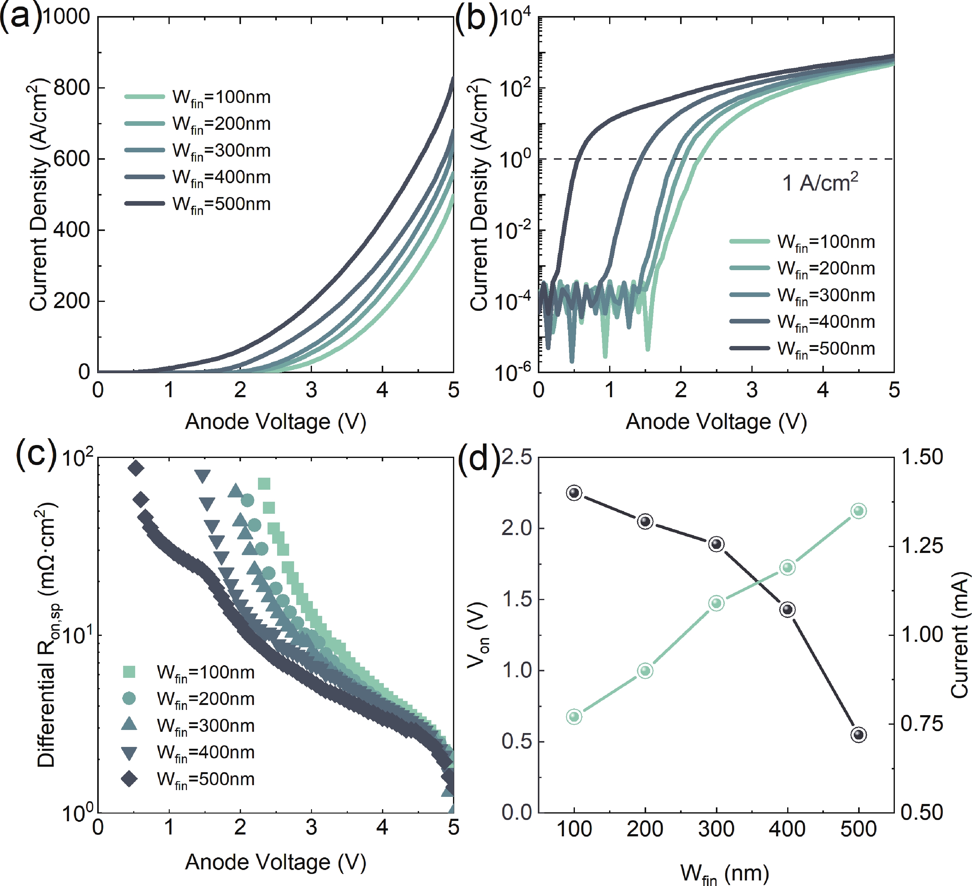
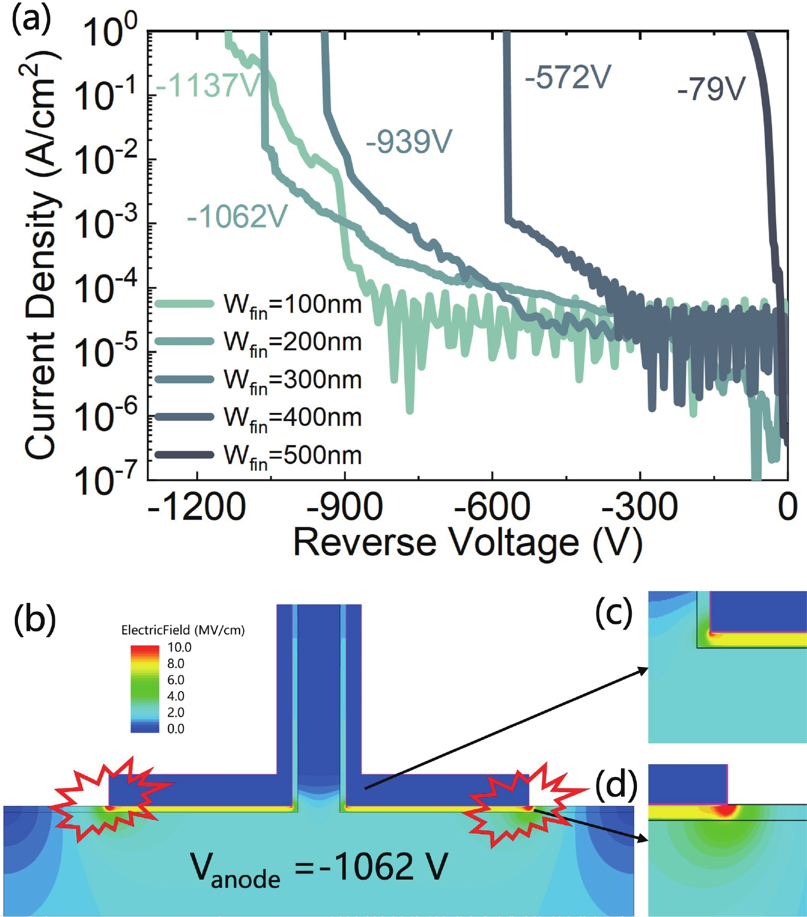
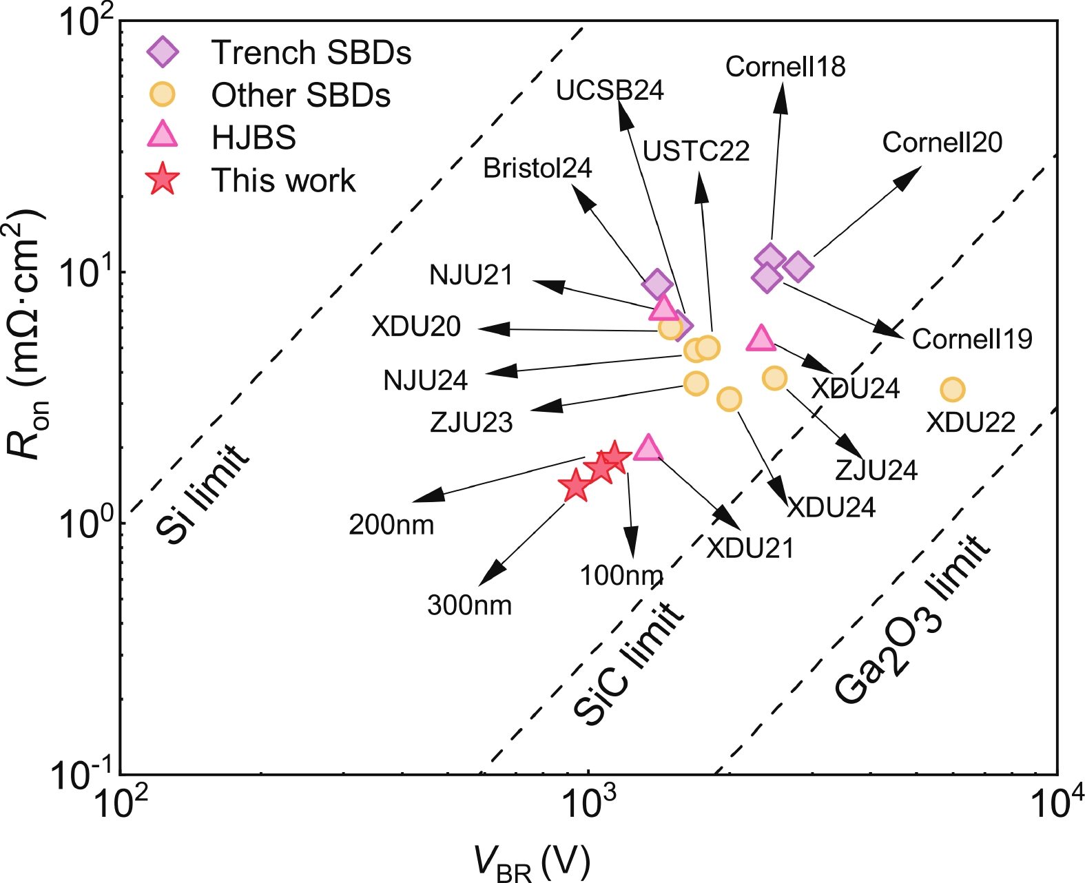
This study presents a β-Ga2O3 diode featuring a Fin-channel structure and an anode ohmic contact. The device turn-off is facilitated by the depletion effect induced by the work function difference between the sidewall metal and β-Ga2O3. As the forward bias increases, electron accumulation occurs on the Fin-channel sidewalls, reducing the on-resistance and improving the forward characteristics. Moreover, the device exhibits the reduced surface field (RESURF) effect, similar to trench schottky barrier diodes (SBDs), which shifts the electric field at the fin corners and enhances the breakdown voltage. For a device with a 100 nm fin width (Wfin), we achieved a breakdown voltage (BV) of 1137 V, a specific on-resistance (Ron,sp) of 1.8 mΩ·cm2, and a power figure of merit (PFOM) of 0.72 GW/cm2. This work expands the fabrication approach for β-Ga2O3-based devices, advancing their potential for high-performance applications.
J. Semicond.
2026, 47(3): 032701 doi: 10.1088/1674-4926/25070039
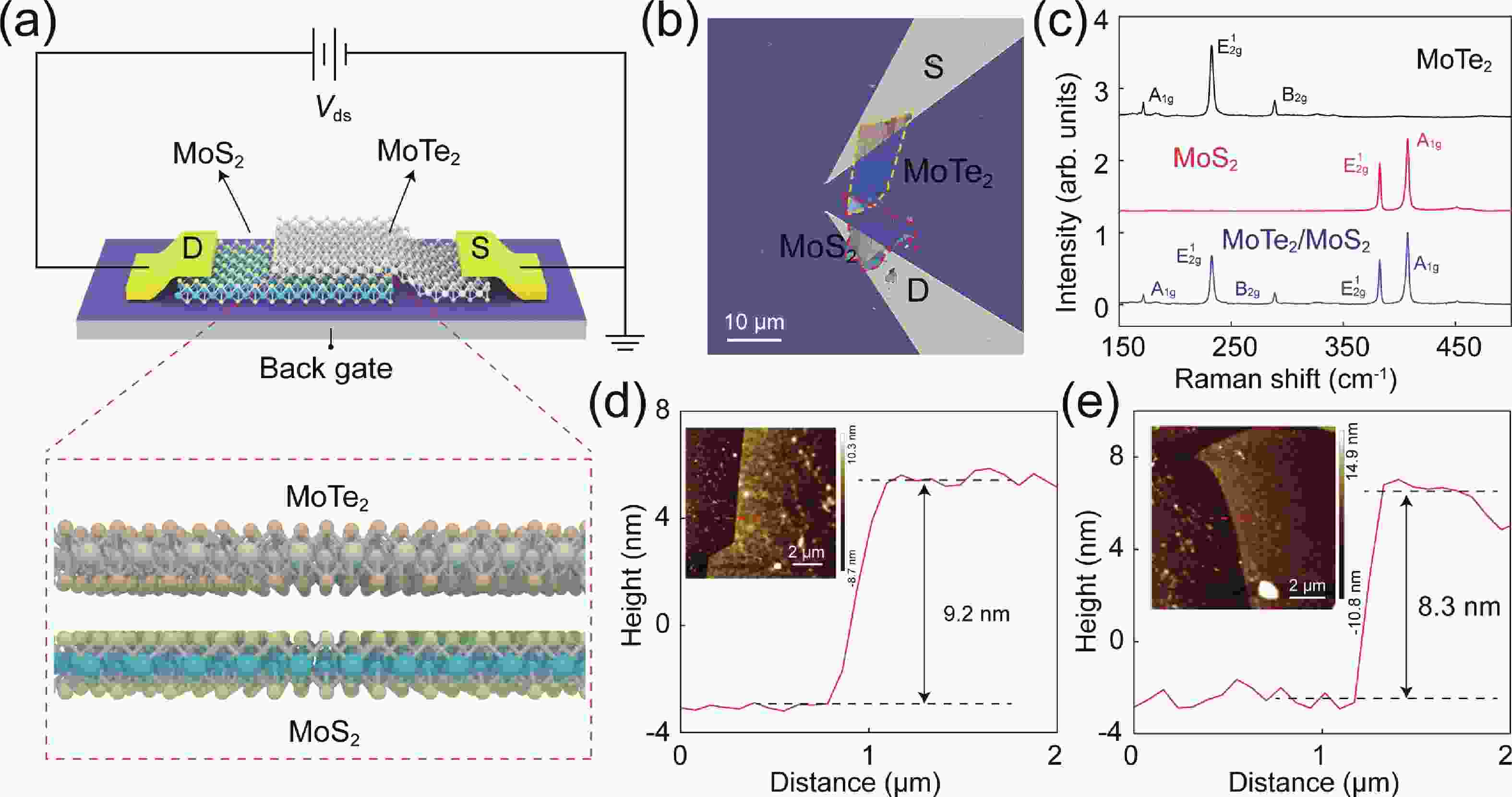
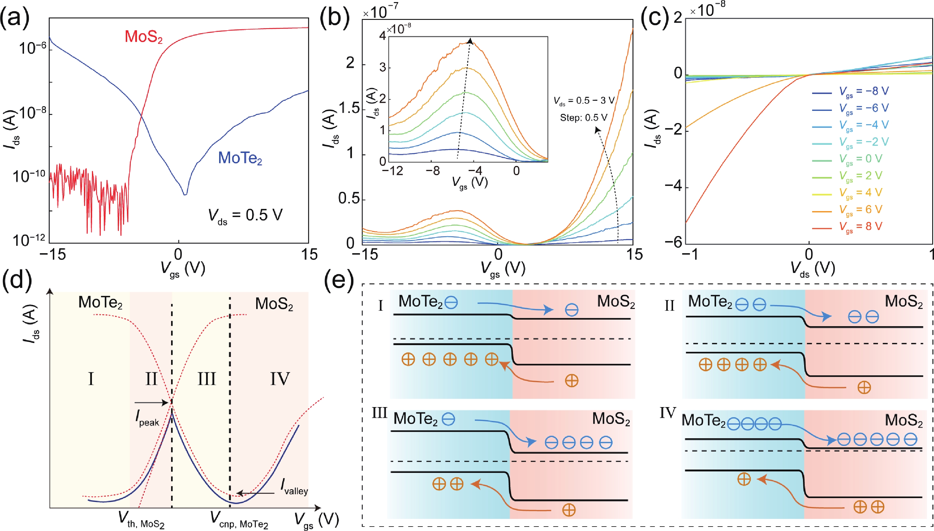
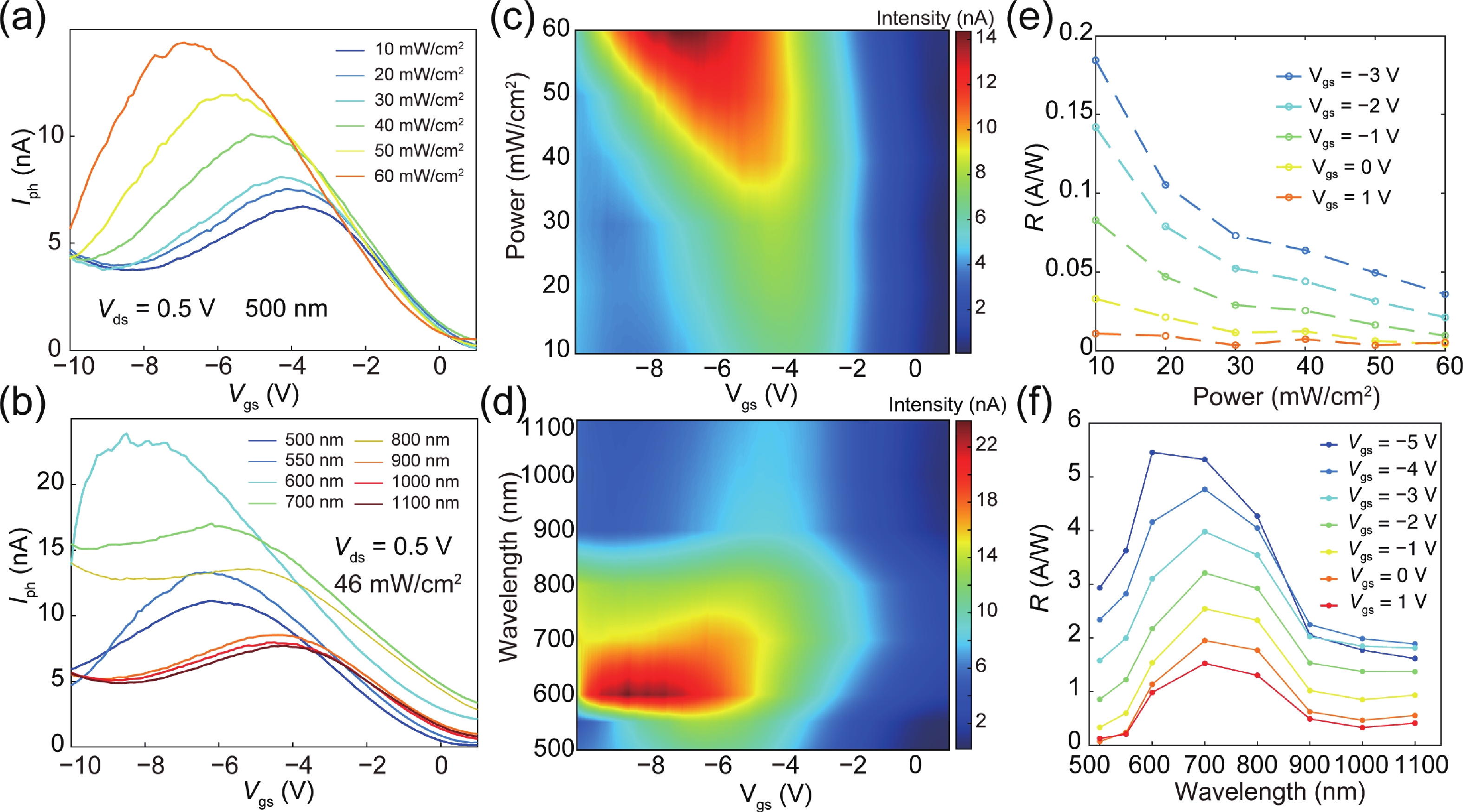
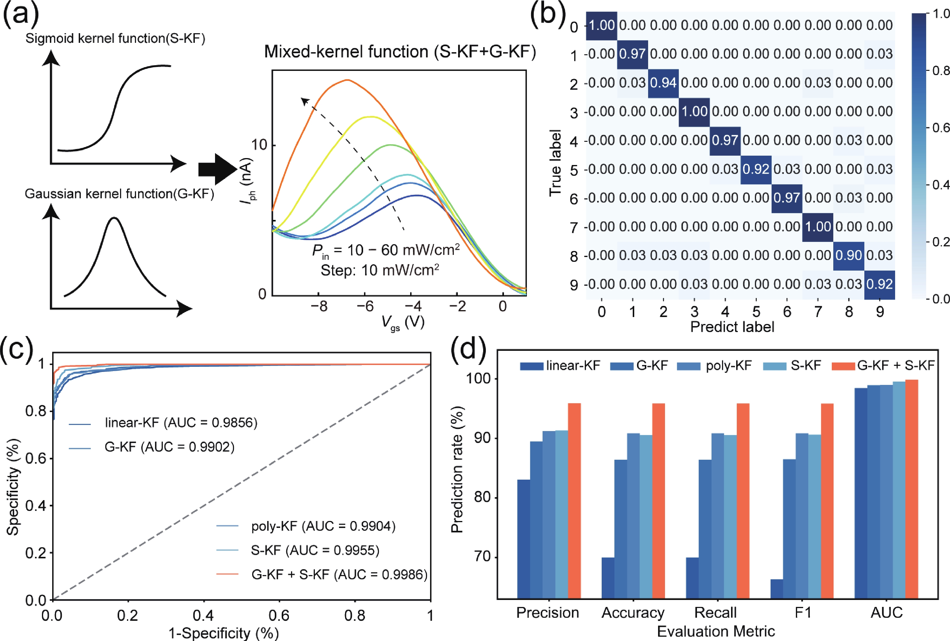
The von Neumann bottleneck in conventional computing architectures presents a significant challenge for data-intensive artificial intelligence applications. A promising approach involves designing specialized hardware with on-chip parameter tunability, which directly accelerates machine learning functions. This work demonstrates a continuously tunable mixed-kernel function physically realized within a van der Waals heterostructure. We designed and fabricated a MoTe2/MoS2 type-Ⅱ vertical heterojunction phototransistor, which exhibits a non-monotonic, Gaussian-like optoelectronic response owing to its unique interlayer charge transfer mechanism. This intrinsic physical behavior directly maps to a mixed-kernel function combining Gaussian and Sigmoid characteristics. Furthermore, the hardware kernel can be continuously modulated by in-situ tuning of external optical stimuli. The mixed-kernel exhibited exceptional performance, achieving precision, accuracy, and area under the curve (AUC) values of 95.8%, 96%, and 0.9986, respectively, significantly outperforming conventional kernels. By successfully embedding a complex, adaptable mathematical function into the intrinsic physical properties of a single device, this work pioneers a novel pathway toward next-generation, energy-efficient intelligent systems with hardware-level adaptability.

J. Semicond.
2026, 47(3): 032702 doi: 10.1088/1674-4926/25060002
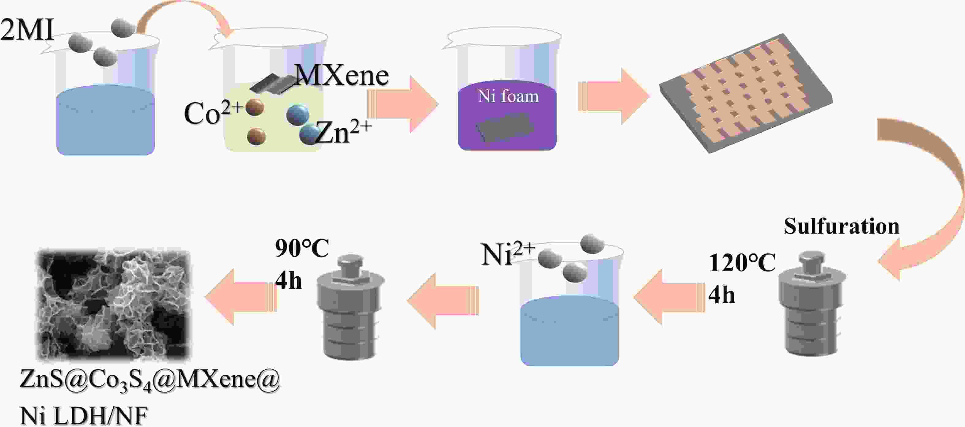
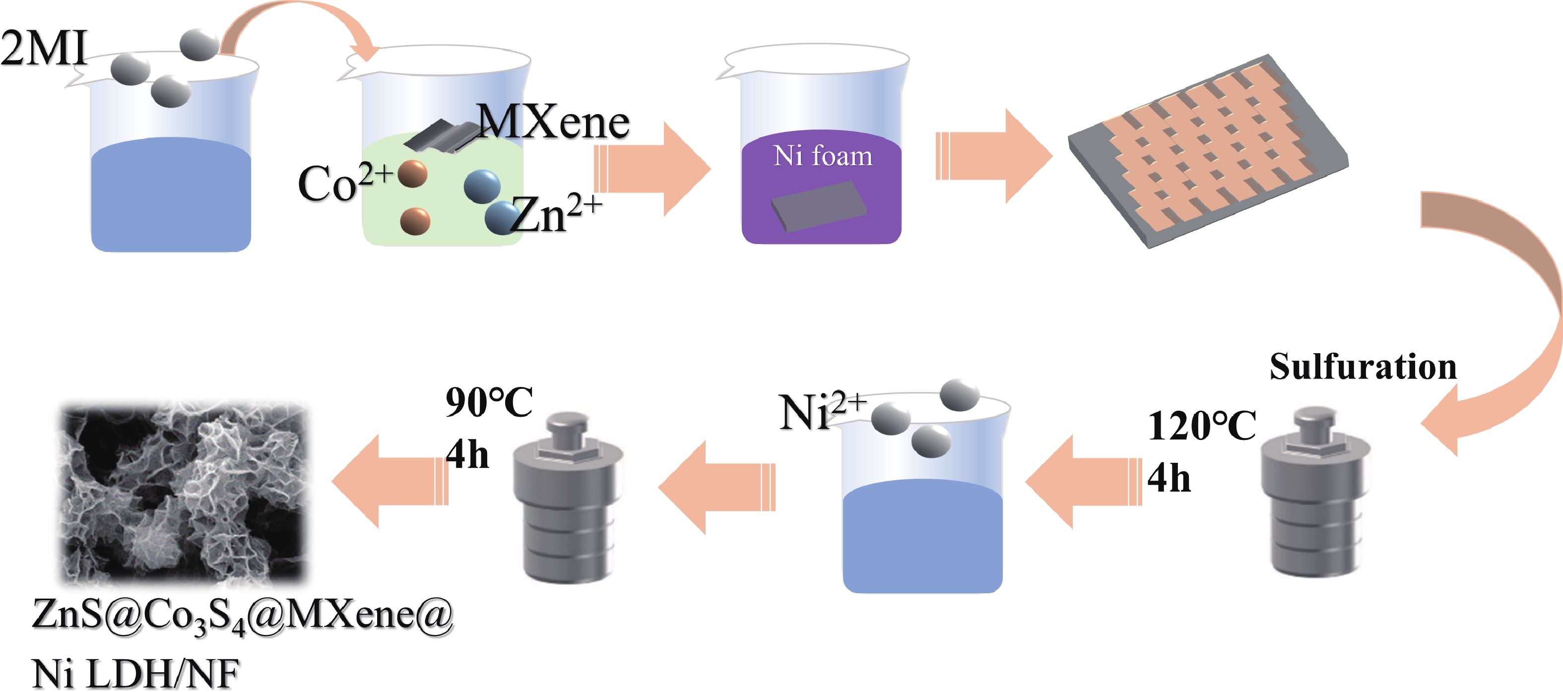
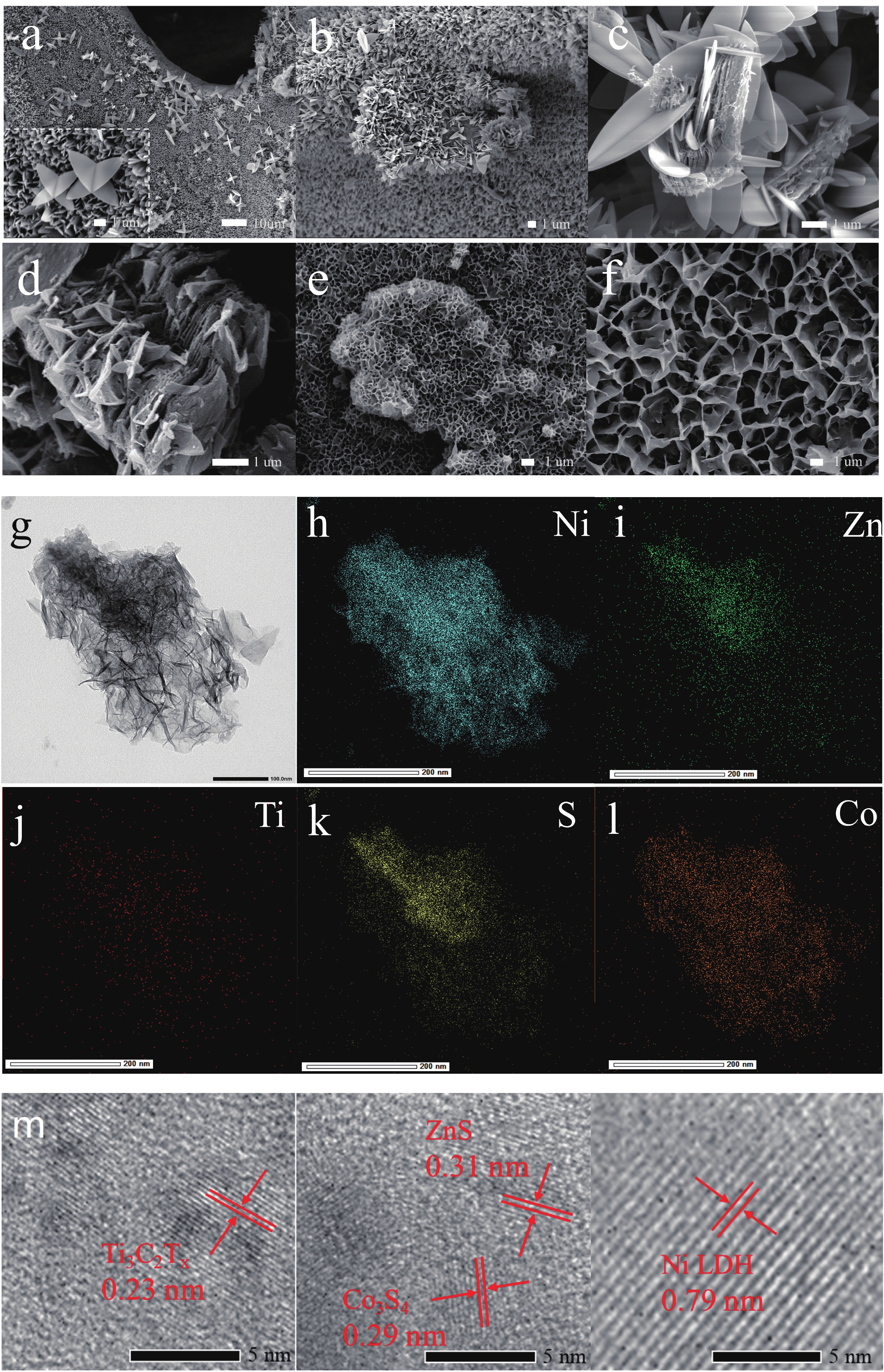
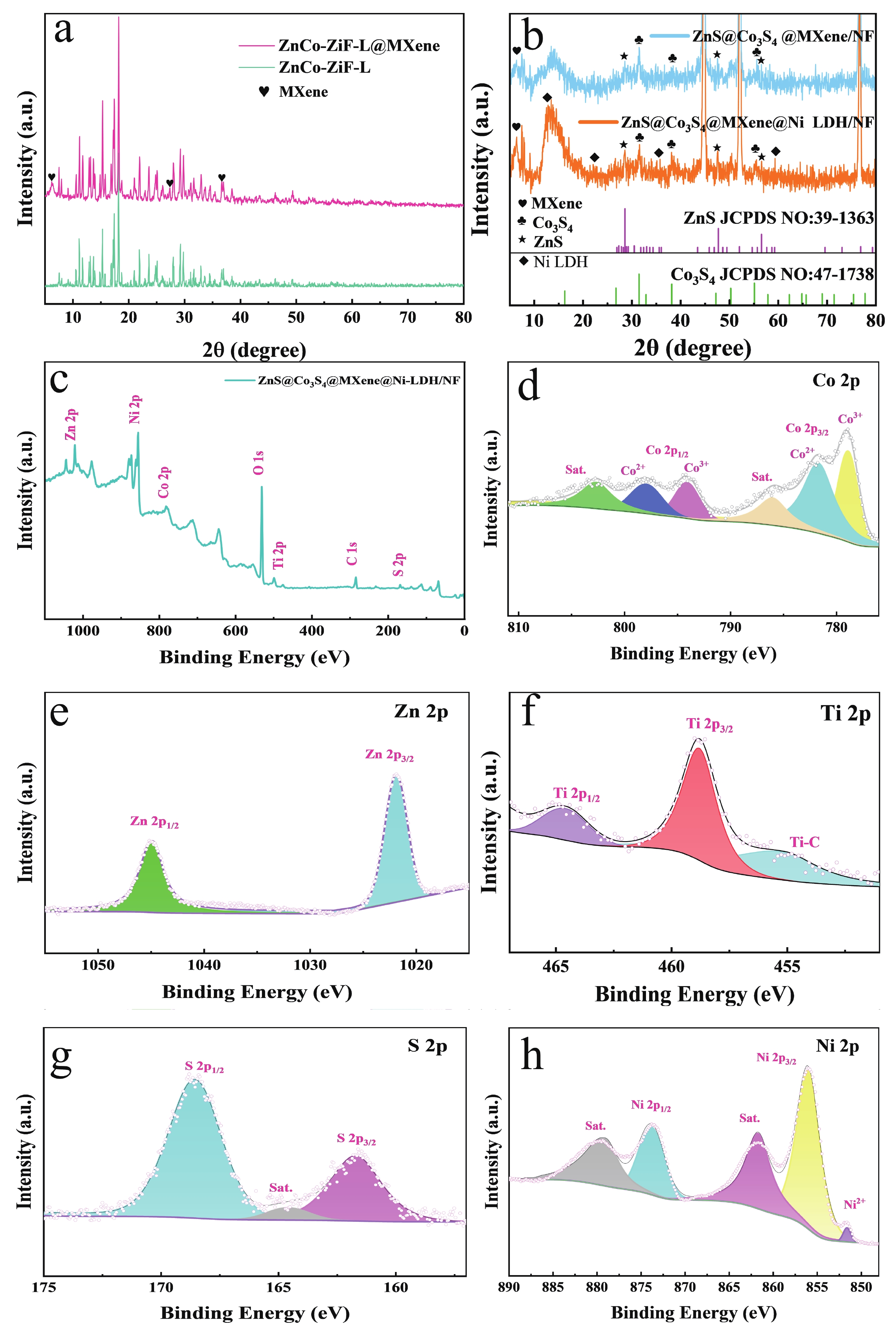
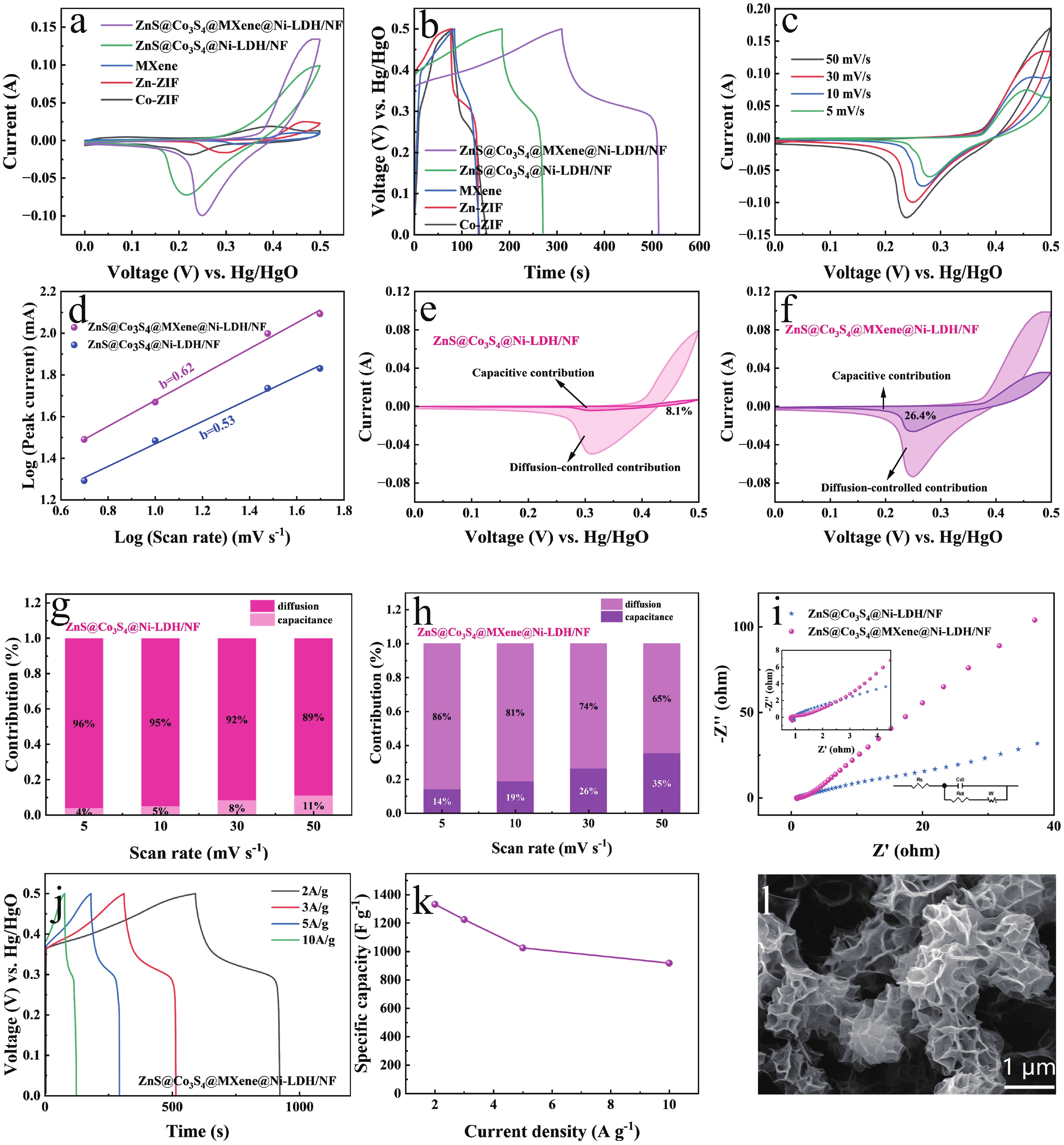
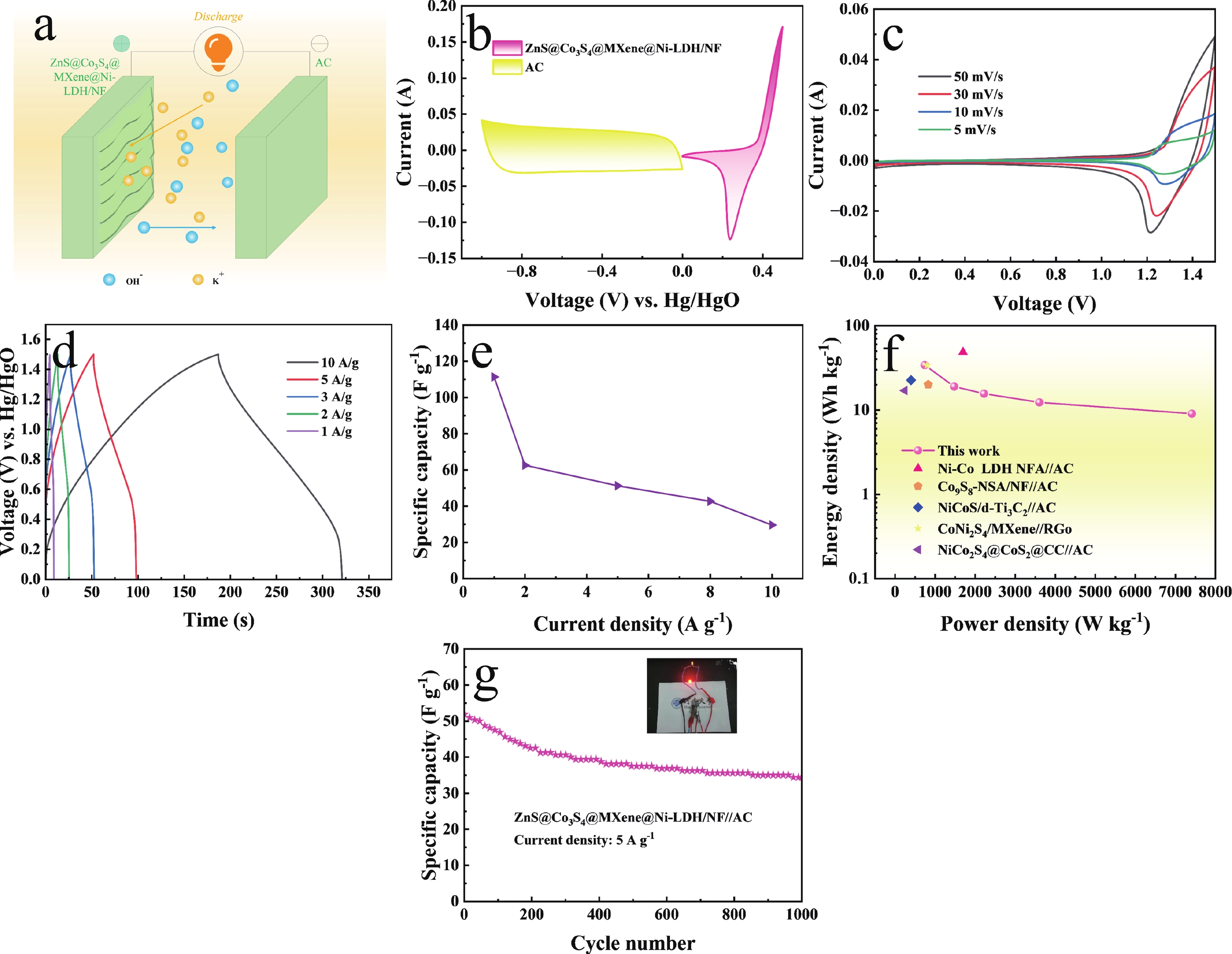
Zeolite imidazolate framework (ZIF)-derived bimetallic sulfides and layered double hydroxides (LDHs) have emerged as promising electrode materials for supercapacitors, owing to their porous layered structures, high electrochemical activity, tunable molecular architectures, low cost, and high specific capacitance. In this study, a unique composite material comprising ZIF-derived ZnCo bimetallic sulfide and LDH with a honeycomb-like structure was in situ grown on nickel foil (NF) via a controlled self-sacrificial template strategy. In contrast to previous reports, the resulting ZnS@Co3S4@MXene@Ni-LDH/NF composite integrates the advantages of MXene, LDH, and sulfides, leading to significantly enhanced conductivity, structural stability, and catalytic activity. The ZnS@Co3S4@MXene@Ni-LDH/NF electrode exhibits a uniform network structure with a thickness of approximately 1 µm coated on NF, and delivers a high specific capacitance of 1356.1 F·g−1 at a current density of 2 A·g−1. Furthermore, an asymmetric supercapacitor assembled with ZnS@Co3S4@MXene@Ni-LDH/NF as the positive electrode and activated carbon as the negative electrode achieves a high energy density of 34.08 Wh·kg−1 and a power density of 742.3 W·kg−1 at 1 A·g−1. This device successfully powers LED lights for 5 min, demonstrating its practical applicability. These results underscore the outstanding electrochemical performance of the ZnS@Co3S4@MXene@Ni-LDH/NF electrode, highlighting its potential for applications in supercapacitors and related energy storage fields.