Issue Browser
Volume 40, Issue 9,
Sep 2019
J. Semicond.
2019, 40(9): 090301 doi: 10.1088/1674-4926/40/9/090301

The 100th anniversary of the birth of Prof. Kun Huang is in this year. Prof. Huang is a paragon of the older generation of Chinese scientists. He had made great achievements in solid state physics. After the founding of the People’s Republic of China, he returned to China immediately, and devoted himself to education. He and Prof. Xide Xie initiated the research of semiconductors in China, and established the solid state physics major at Peking University, which has trained a large number of talents for China. In 1977, he became the director of the Institute of Semiconductors of the Chinese Academy of Sciences. Led by Prof. Huang, together with Prof. Shouwu Wang, Prof. Lanying Lin and Prof. Shoujue Wang, the semiconductor institute independently overcomes many difficulties and created a group of critical devices which were on international embargo but urgently needed by China. Furthermore, he also made new contributions in the field of semiconductor superlattices. Under his leadership, the State Key Laboratory of Semiconductor Superlattices became one of the internationally leading laboratories. The following are the major scientific contributions of Prof. Kun Huang.


J. Semicond.
2019, 40(9): 090102 doi: 10.1088/1674-4926/40/9/090102
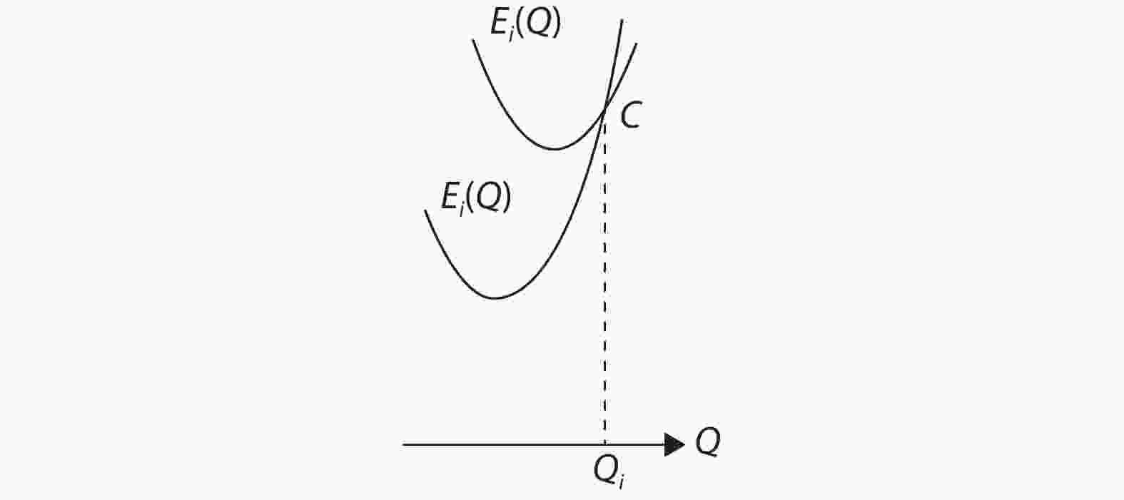
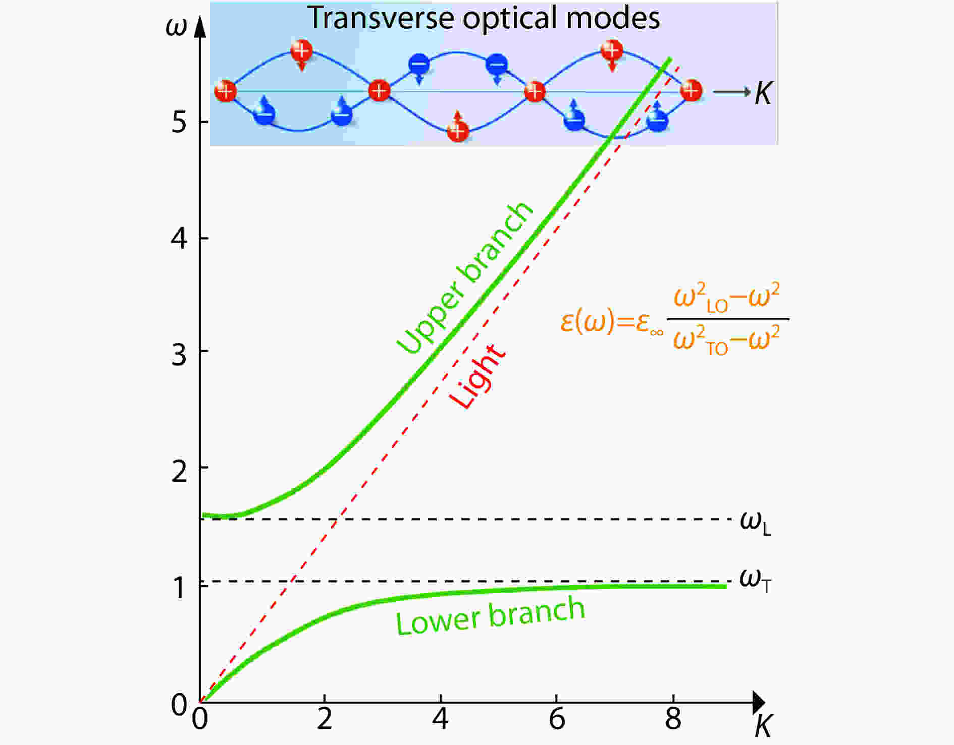
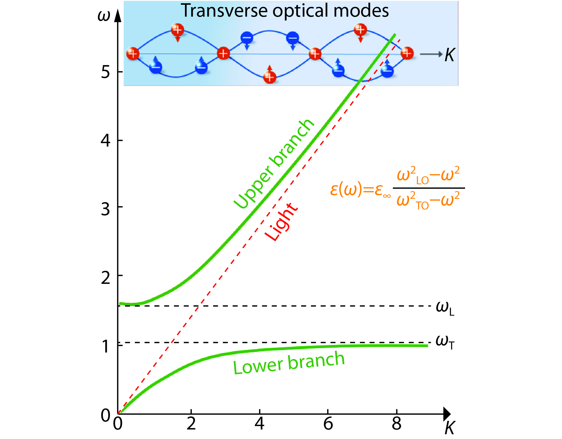
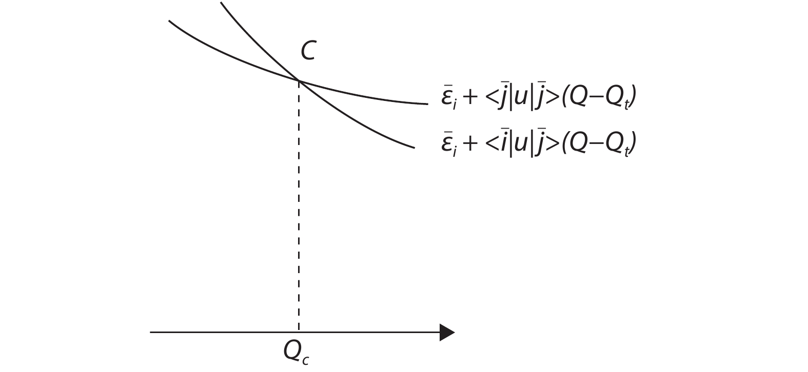
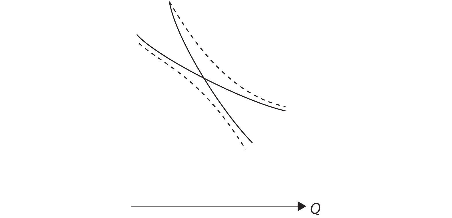
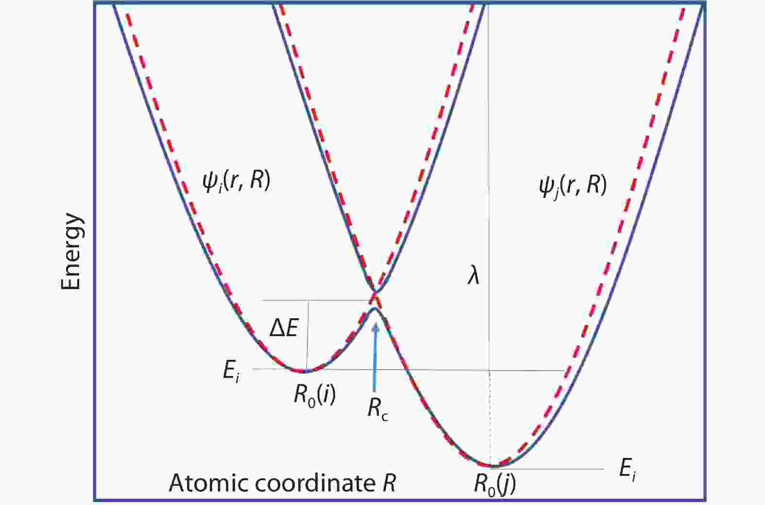
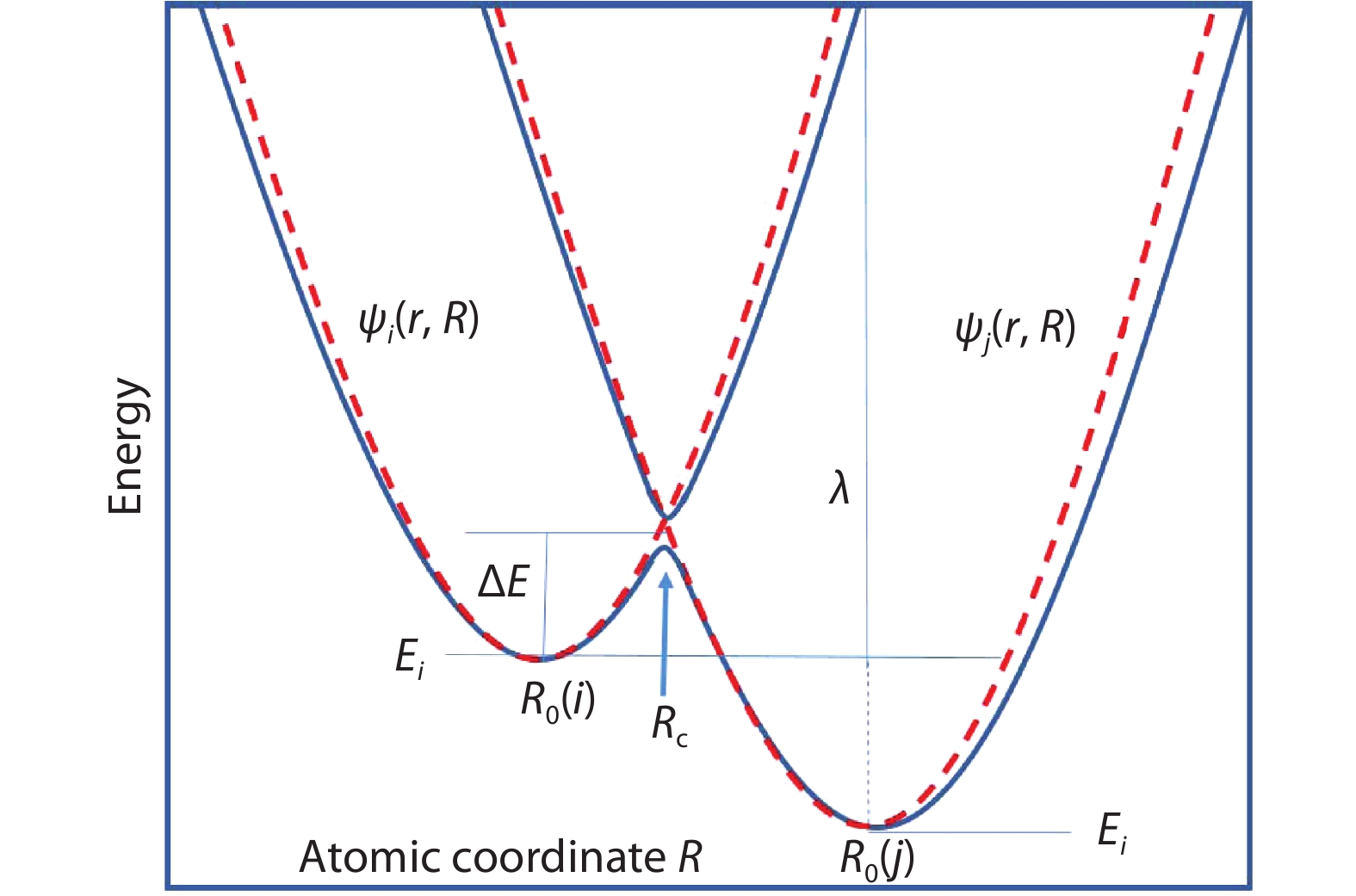
A recent paper by C. H. Henry and D. V. Lang claims that the adiabatic approximation breaks down in the neighborhood of the intersection of the adiabatic potential curves for the two electronic states, between which multiphonon transitions occur. It is shown that their claim is not justified; what they consider to be the sign of failure of the adiabatic approximation is no more than an indication of the fact that owing to the uncertainty principle, there is a finite neighborhood around the above mentioned point of intersection, throughout which multi-phonon transitions can occur. Direct calculation of the multi-phonon transition probability on the basis of the adiabatic approximation gives in fact a result identical with the result obtained with their version of the theory. Further discussions contend that in more general situations Henry and Lang’s formulation of the theory will no longer be applicable and a proper adiabatic approximation treatment by first lifting the degeneracy at the intersection point will be necessary.

J. Semicond.
2019, 40(9): 091001 doi: 10.1088/1674-4926/40/9/091001
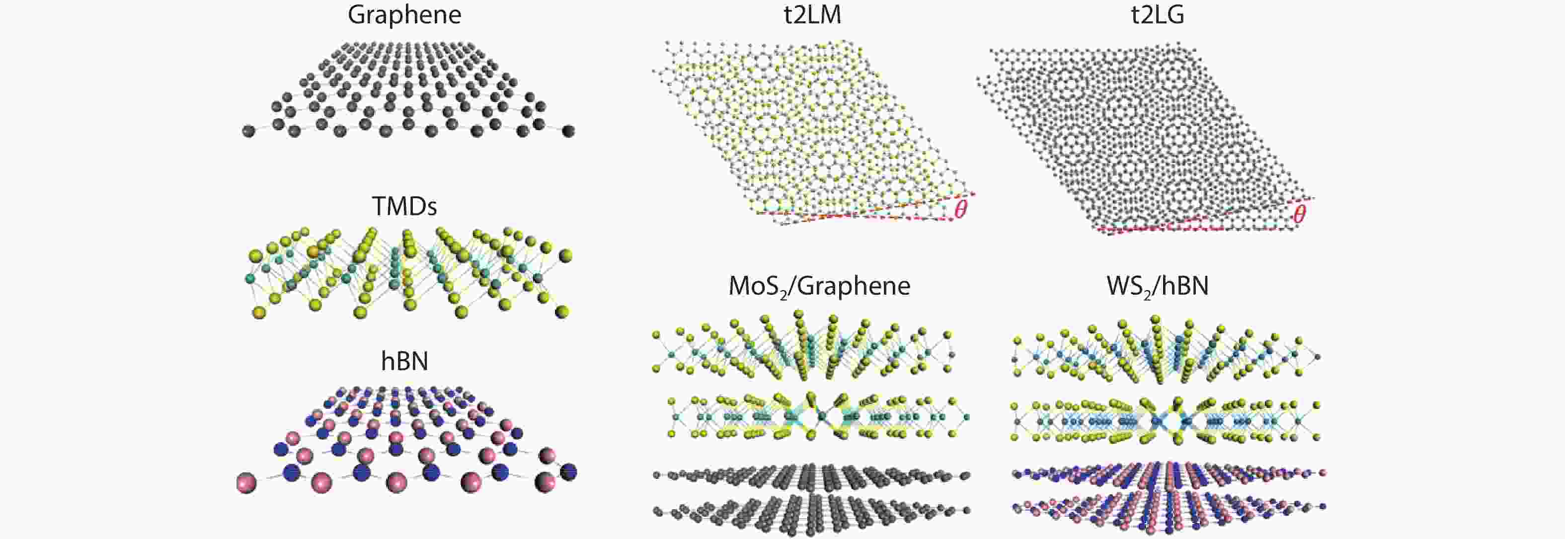
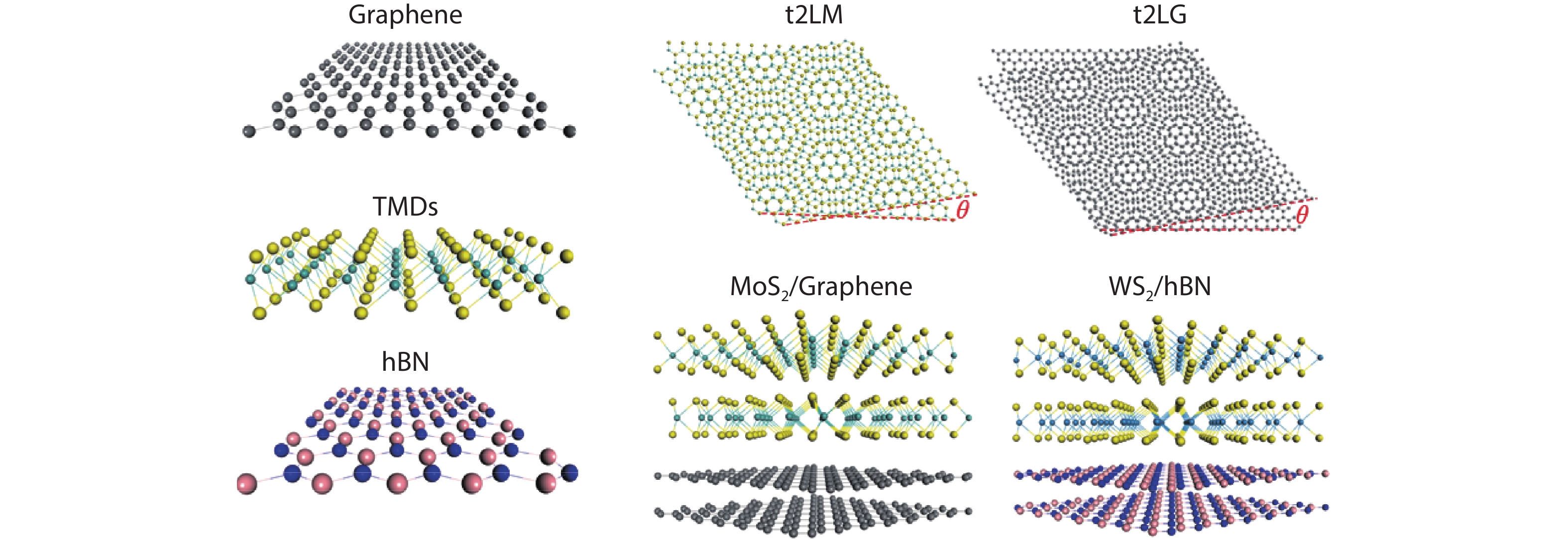
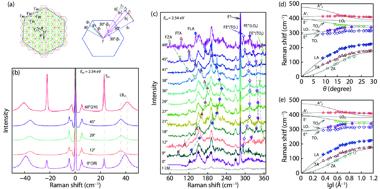
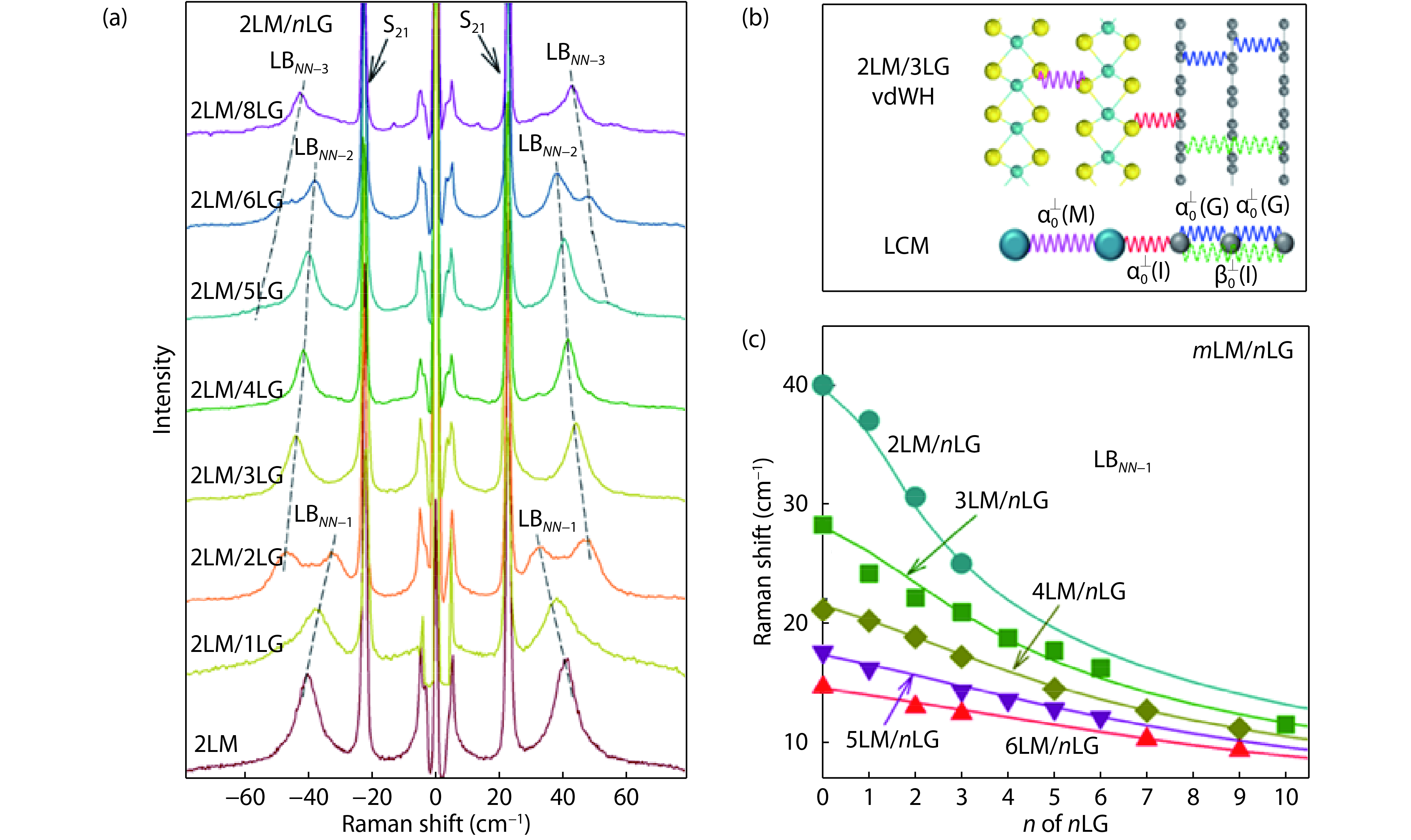
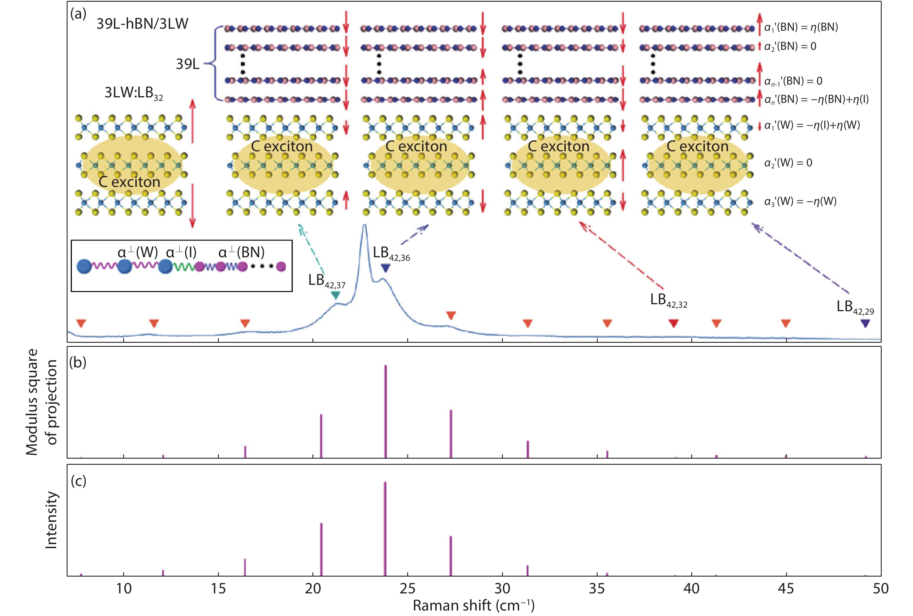
Research on two-dimensional (2D) materials and related van der Waals heterostructures (vdWHs) is intense and remains one of the leading topics in condensed matter physics. Lattice vibrations or phonons of a vdWH provide rich information, such as lattice structure, phonon dispersion, electronic band structure and electron–phonon coupling. Here, we provide a mini review on the lattice vibrations in vdWHs probed by Raman spectroscopy. First, we introduced different kinds of vdWHs, including their structures, properties and potential applications. Second, we discussed interlayer and intralayer phonon in twist multilayer graphene and MoS2. The frequencies of interlayer and intralayer modes can be reproduced by linear chain model (LCM) and phonon folding induced by periodical moiré potentials, respectively. Then, we extended LCM to vdWHs formed by distinct 2D materials, such as MoS2/graphene and hBN/WS2 heterostructures. We further demonstrated how to calculate Raman intensity of interlayer modes in vdWHs by interlayer polarizability model.

J. Semicond.
2019, 40(9): 091002 doi: 10.1088/1674-4926/40/9/091002

The growing demand for high-performance logic transistors has driven the exponential rise in chip integration, while the transistors have been rapidly scaling down to sub-10 nm. The increasing leakage current and subthreshold slope (SS) induced by short channel effect (SCE) result in extra heat dissipation during device operation. The performance of electronic devices based on two-dimensional (2D) semiconductors such as the transition metal dichalcogenides (TMDC) can significantly reduce power consumption, benefiting from atomically thin thickness. Here, we discuss the progress of dielectric integration of 2D metal–oxide–semiconductor field effect transistors (MOSFETs) and 2D negative capacitance field effect transistors (NCFETs), outlining their potential in low-power applications as a technological option beyond scaled logic switches. Above all, we show our perspective at 2D low-power logic transistors, including the ultra-thin equivalent oxide thickness (EOT), reducing density of interface trap, reliability, operation speed etc. of 2D MOSFETs and NCFETs.


J. Semicond.
2019, 40(9): 091101 doi: 10.1088/1674-4926/40/9/091101
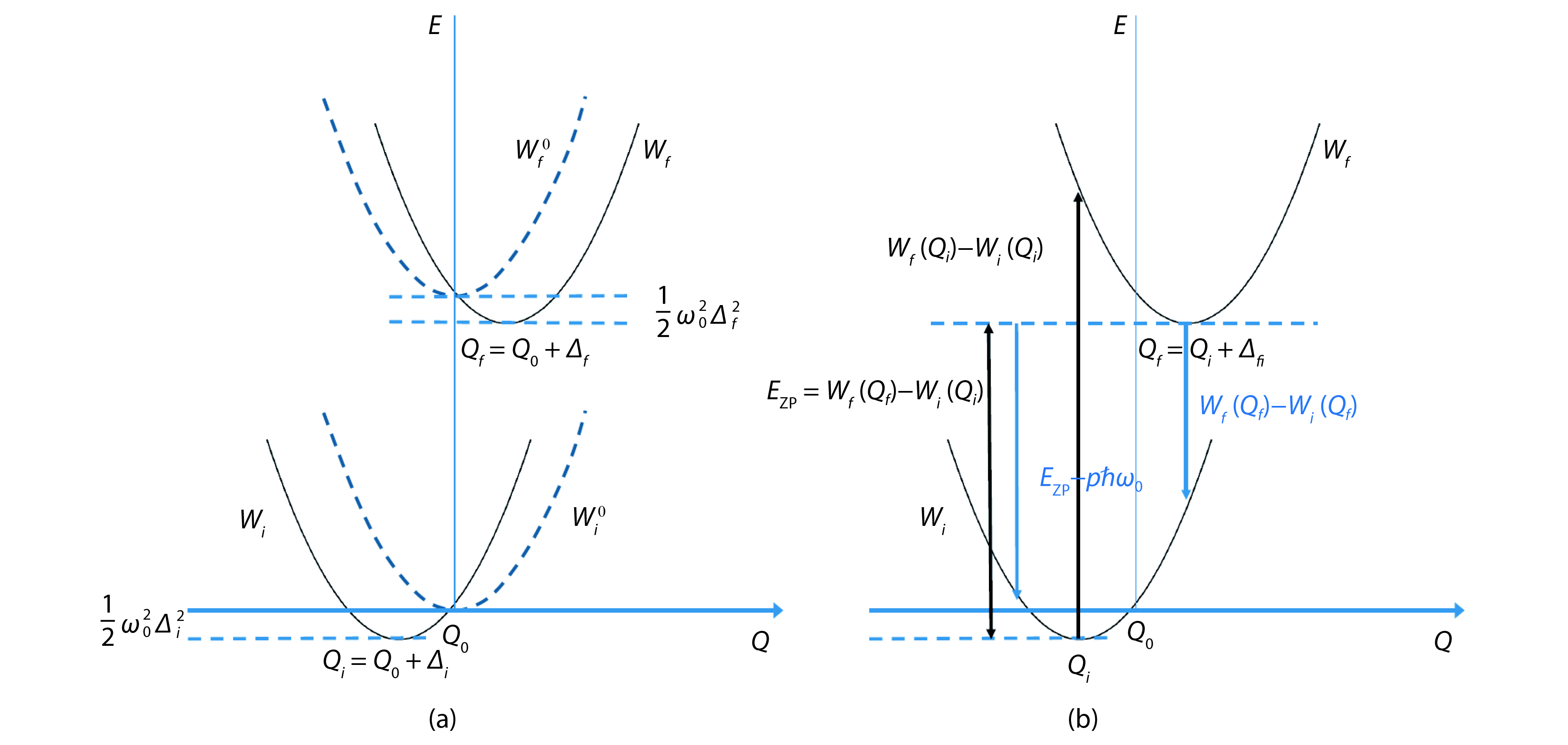
In this short review, we discuss a few recent advances in calculating the nonradiative decay rates for point defects in semiconductors. We briefly review the debates and connections of using different formalisms to calculate the multi-phonon processes. We connect Dr. Huang’s formula with Marcus theory formula in the high temperature limit, and point out that Huang’s formula provide an analytical expression for the phonon induced electron coupling constant in the Marcus theory formula. We also discussed the validity of 1D formula in dealing with the electron transition processes, and practical ways to correct the anharmonic effects.
J. Semicond.
2019, 40(9): 091102 doi: 10.1088/1674-4926/40/9/091102
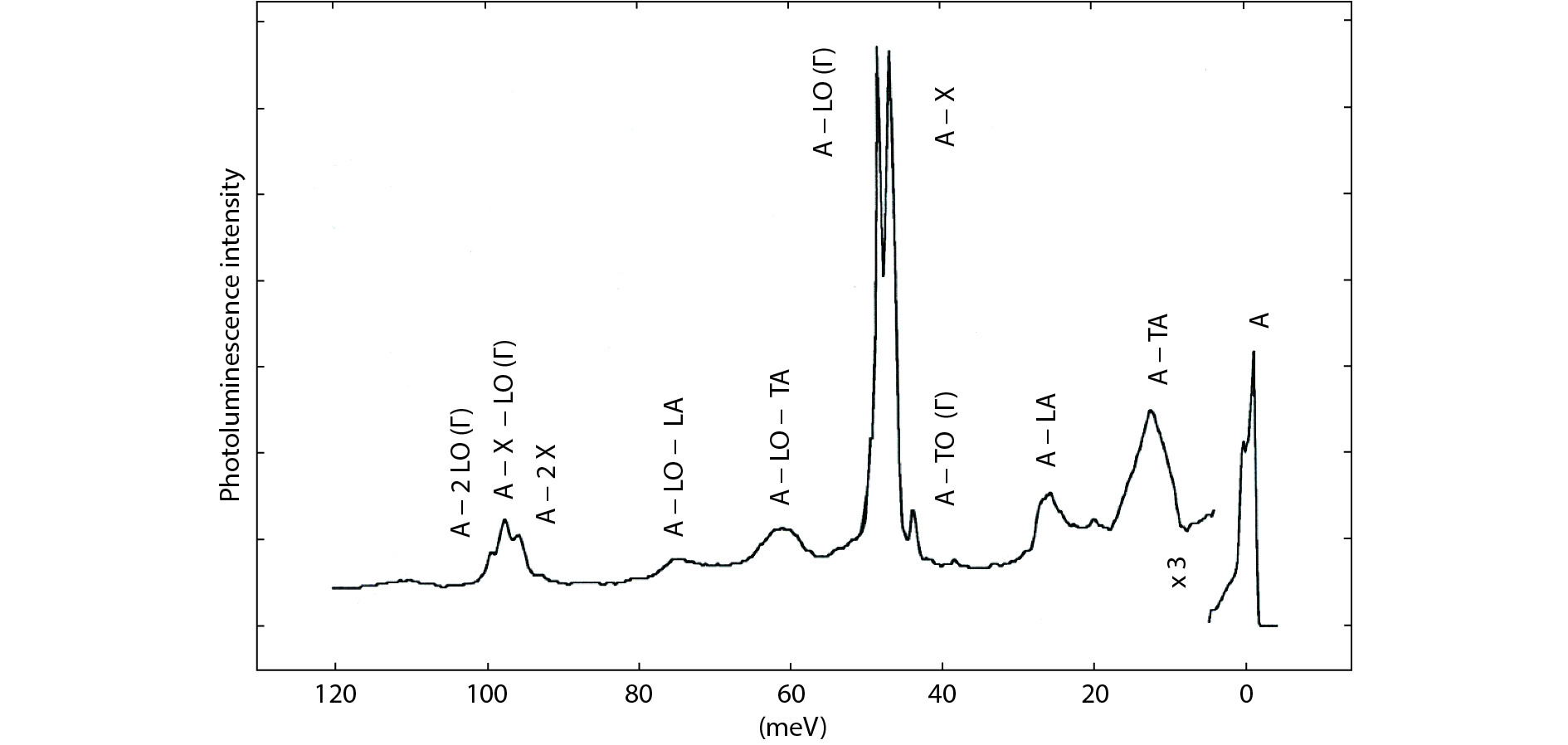
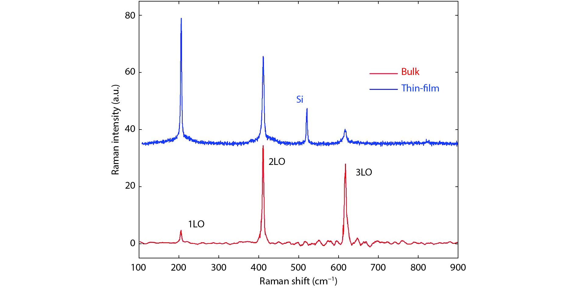
A brief review of Huang–Rhys theory and Albrechtos theory is provided, and their connection and applications are discussed. The former is a first order perturbative theory on optical transitions intended for applications such as absorption and emission involving localized defect or impurity centers, emphasizing lattice relaxation or mixing of vibrational states due to electron–phonon coupling. The coupling strength is described by the Huang–Rhys factor. The latter theory is a second order perturbative theory on optical transitions intended for Raman scattering, and can in-principle include electron–phonon coupling in both electronic states and vibrational states. These two theories can potentially be connected through the common effect of lattice relaxation – non-orthonormal vibrational states associated with different electronic states. Because of this perceived connection, the latter theory is often used to explain resonant Raman scattering of LO phonons in bulk semiconductors and further used to describe the size dependence of electron–phonon coupling or Huang–Rhys factor in semiconductor nanostructures. Specifically, the A term in Albrechtos theory is often invoked to describe the multi-LO-phonon resonant Raman peaks in both bulk and nanostructured semiconductors in the literature, due to the misconception that a free-exciton could have a strong lattice relaxation. Without lattice relaxation, the A term will give rise to Rayleigh or elastic scattering. Lattice relaxation is only significant for highly localized defect or impurity states, and should be practically zero for either single particle states or free exciton states in a bulk semiconductor or for confined states in a semiconductor nanostructure that is not extremely small.
J. Semicond.
2019, 40(9): 092001 doi: 10.1088/1674-4926/40/9/092001
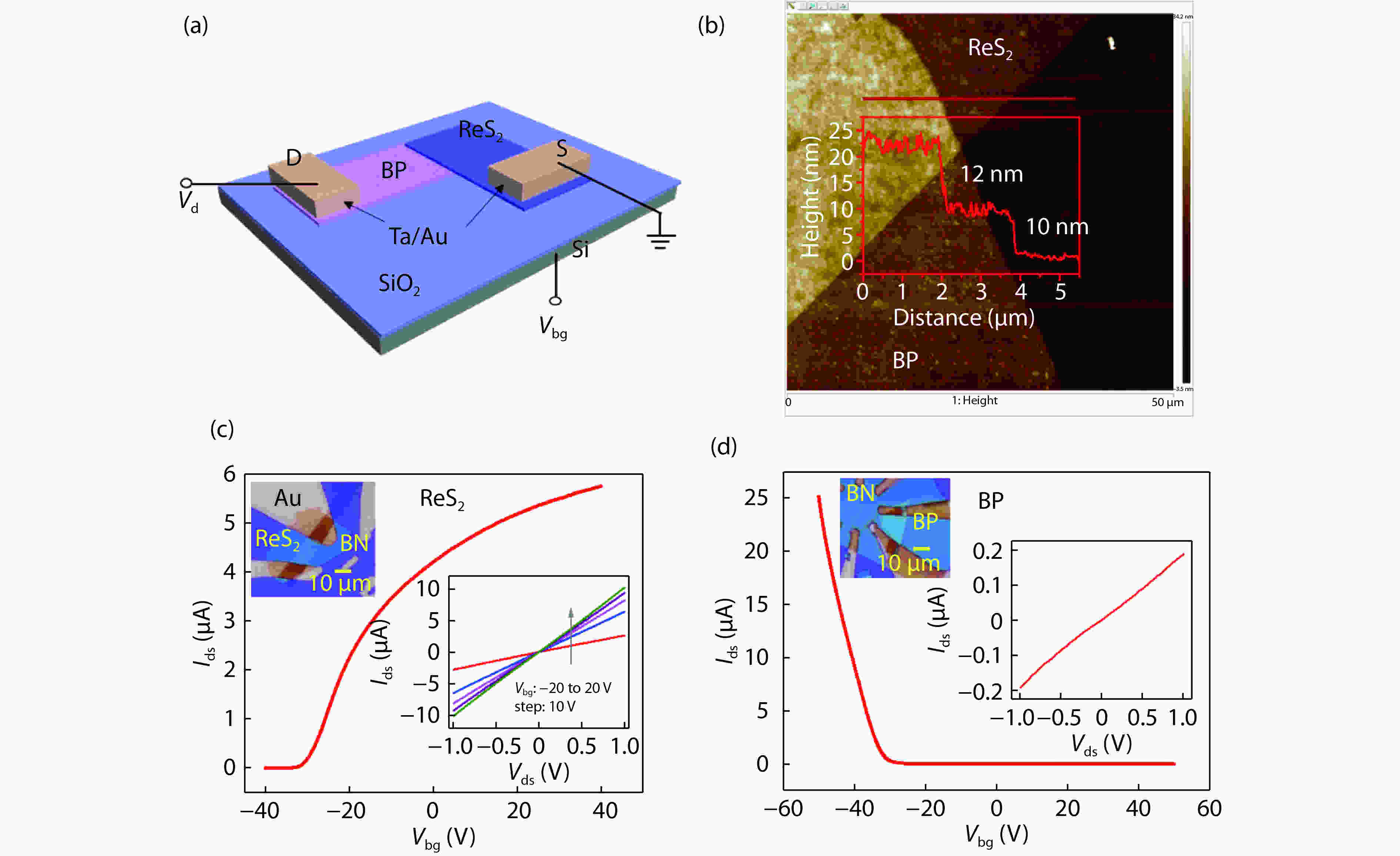
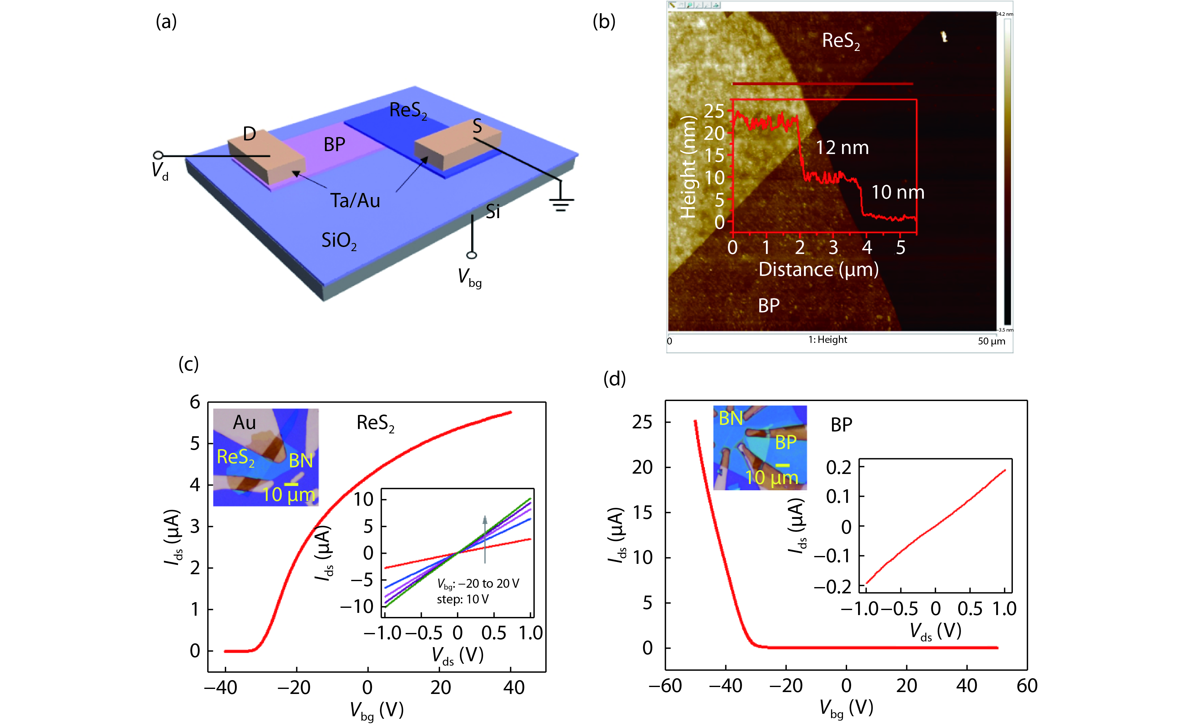
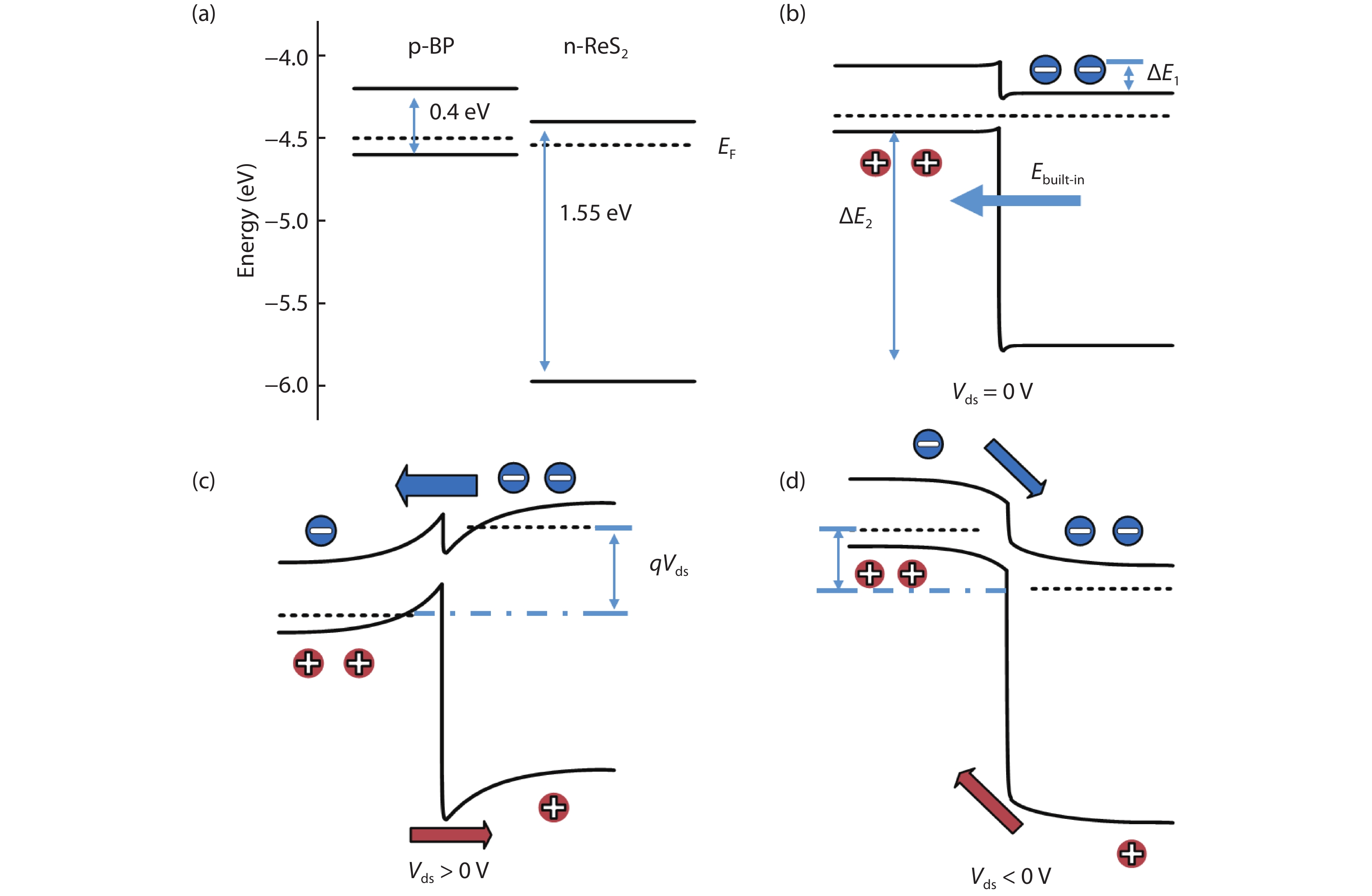
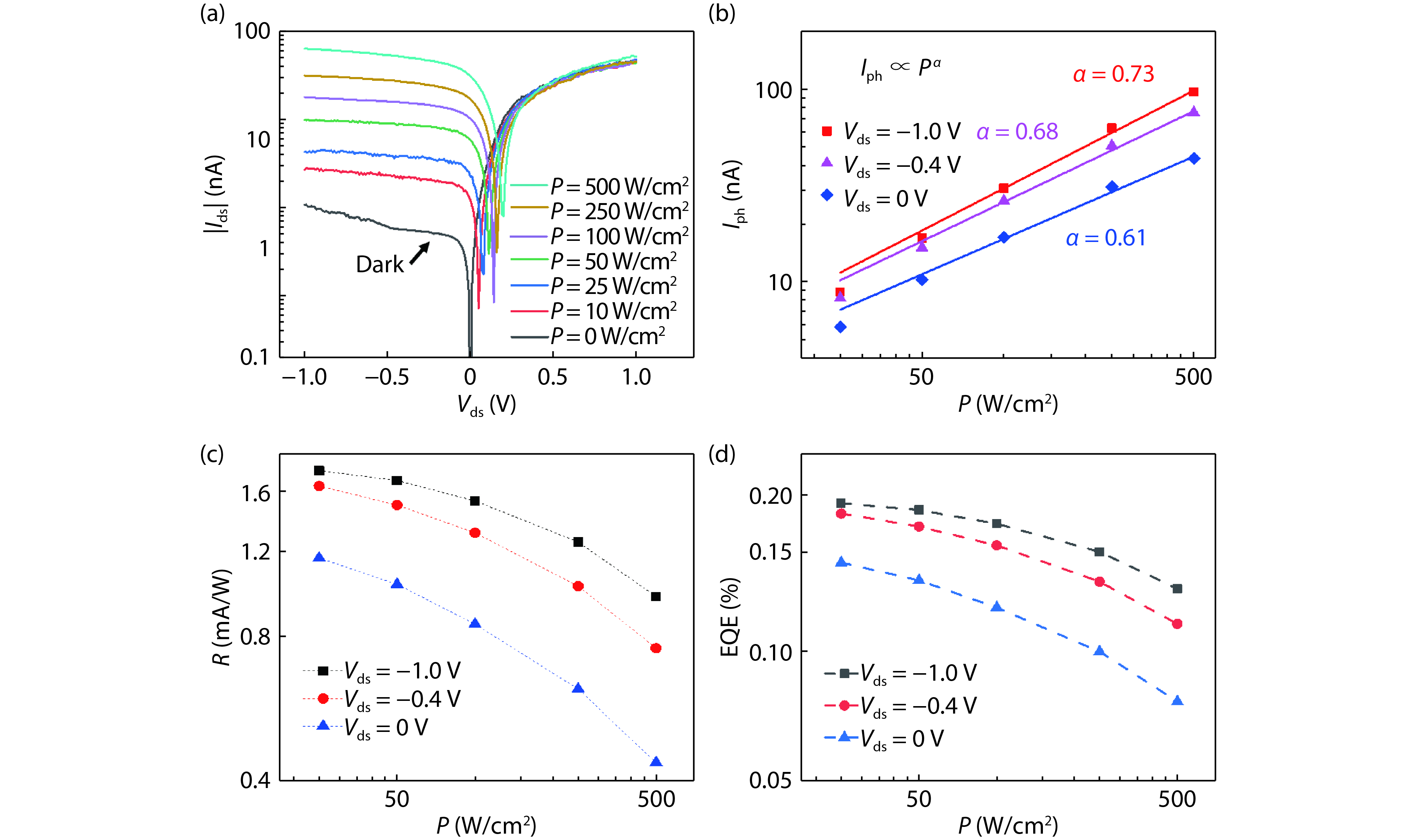
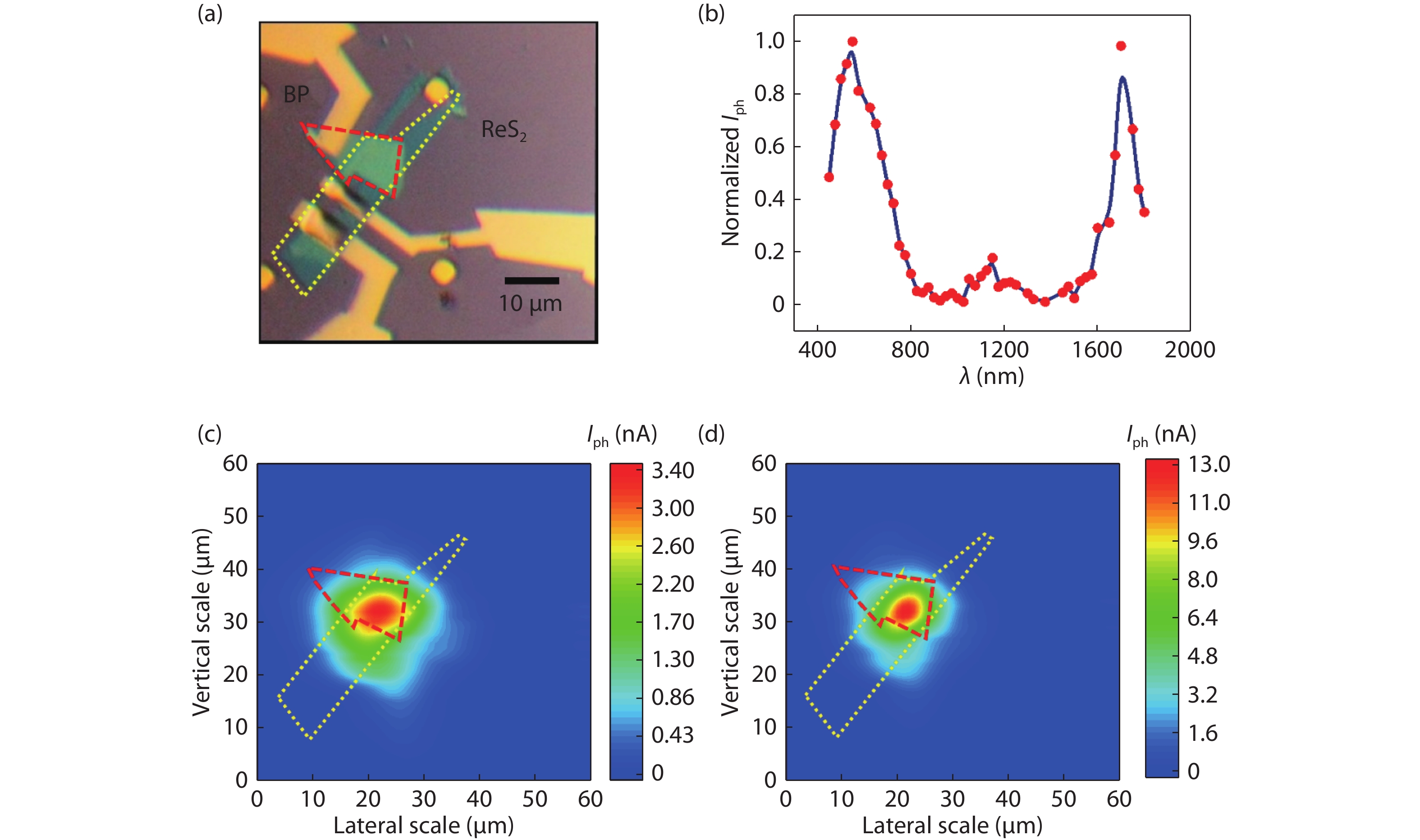
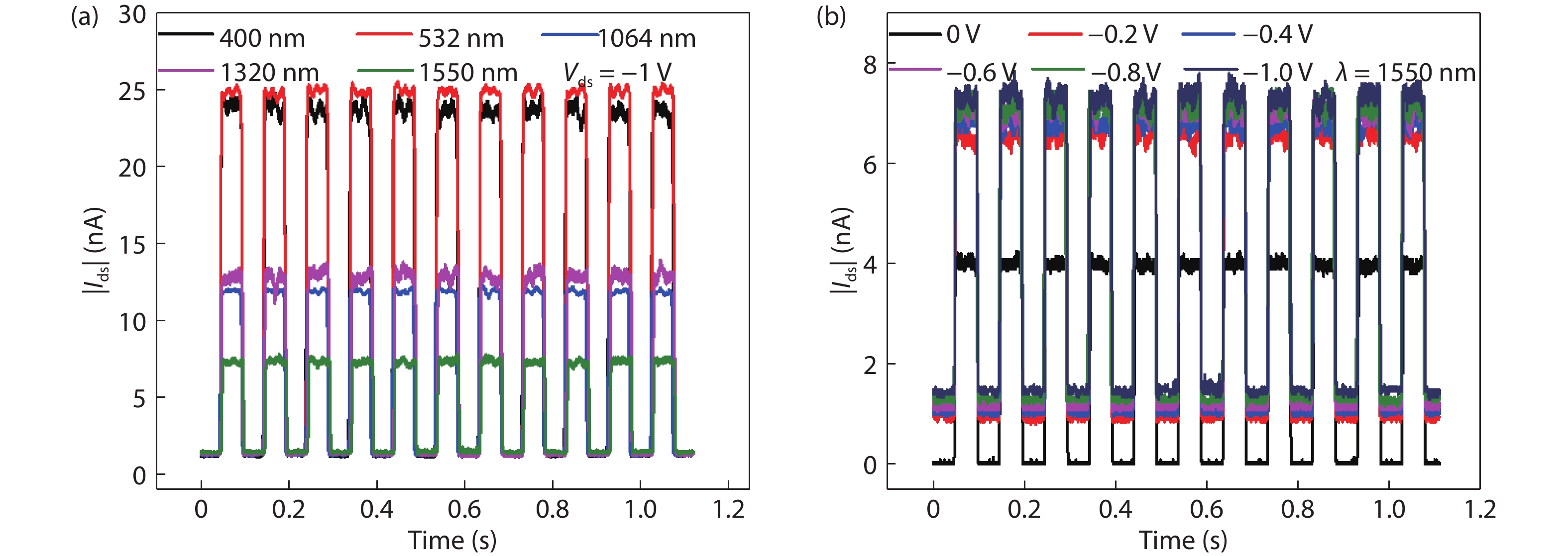
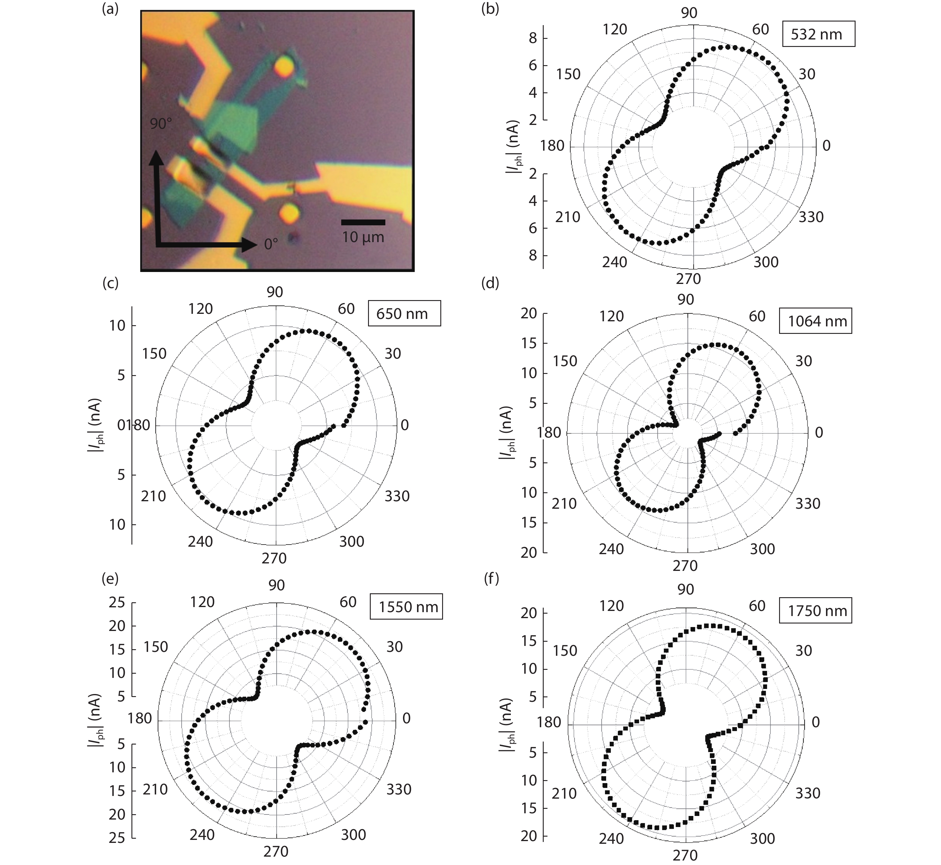
Two-dimensional (2D) atomic crystals, such as graphene, black phosphorus (BP) and transition metal dichalcogenides (TMDCs) are attractive for use in optoelectronic devices, due to their unique crystal structures and optical absorption properties. In this study, we fabricated BP/ReS2 van der Waals (vdWs) heterojunction devices. The devices realized broadband photoresponse from visible to near infrared (NIR) (400–1800 nm) with stable and repeatable photoswitch characteristics, and the photoresponsivity reached 1.8 mA/W at 1550 nm. In addition, the polarization sensitive detection in the visible to NIR spectrum (532–1750 nm) was demonstrated, and the photodetector showed a highly polarization sensitive photocurrent with an anisotropy ratio as high as 6.44 at 1064 nm. Our study shows that van der Waals heterojunction is an effective way to realize the broadband polarization sensitive photodetection, which is of great significance to the realization and application of multi-functional devices based on 2D vdWs heterostructures.
J. Semicond.
2019, 40(9): 092002 doi: 10.1088/1674-4926/40/9/092002
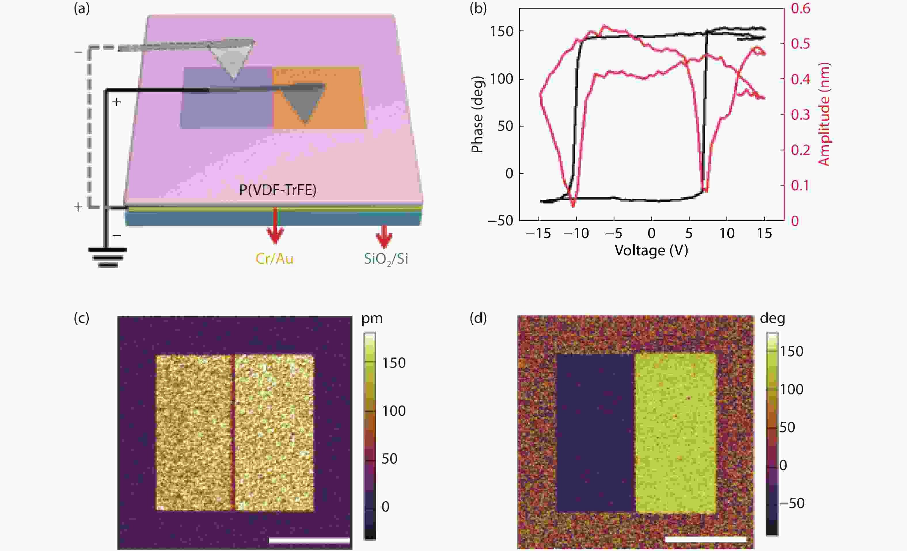
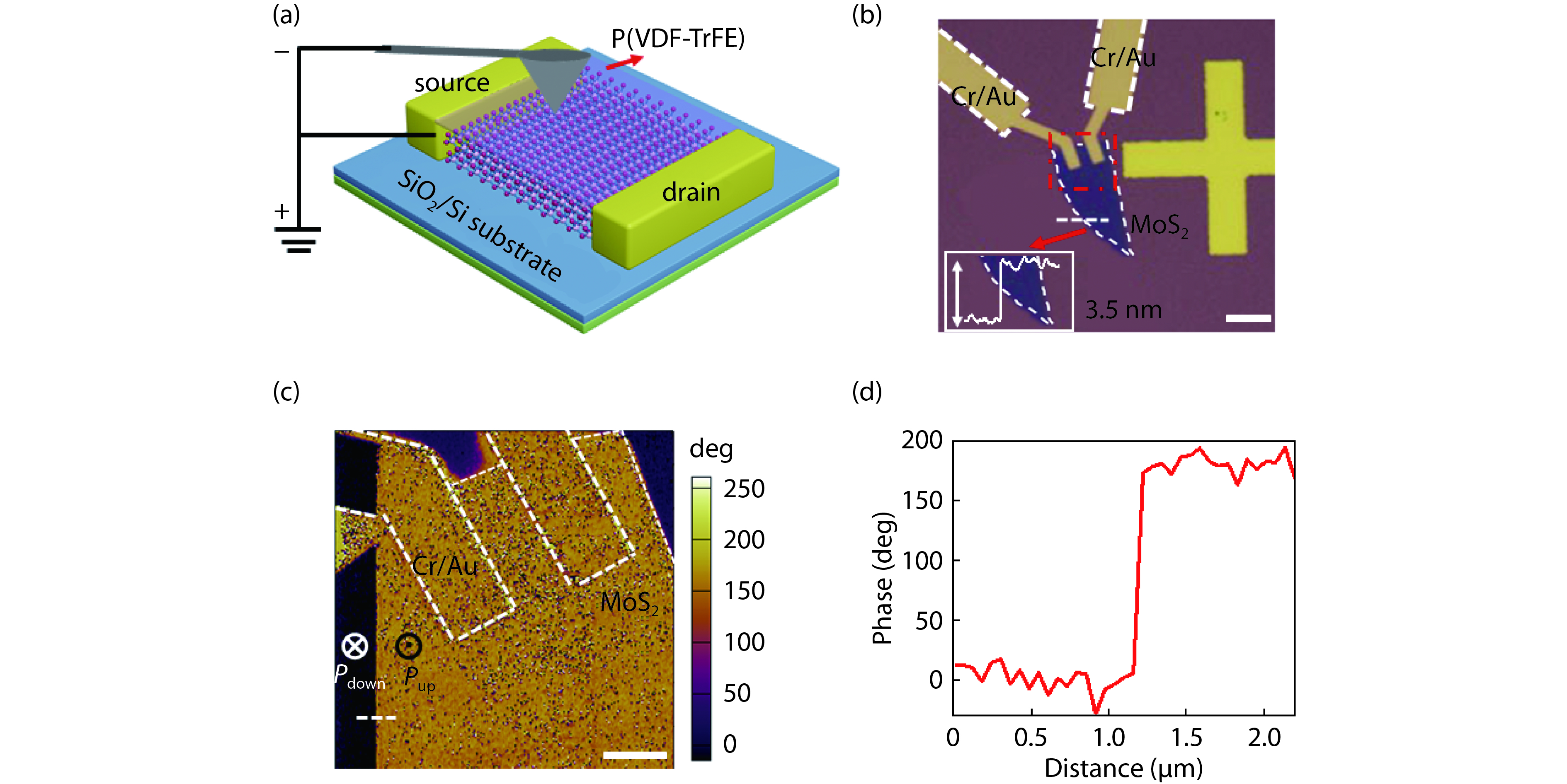
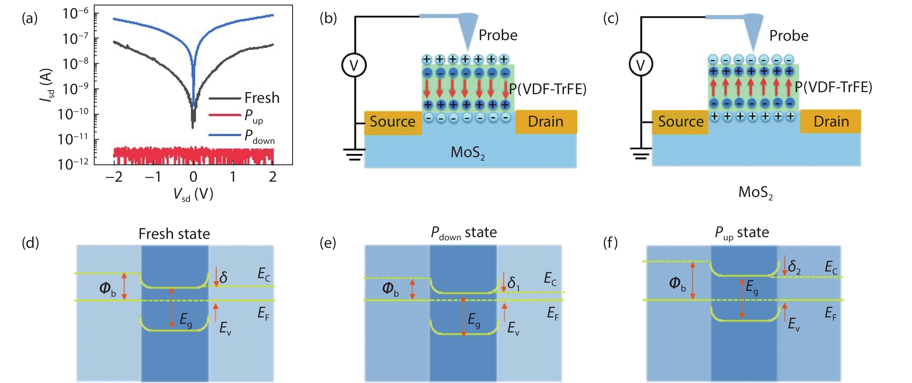
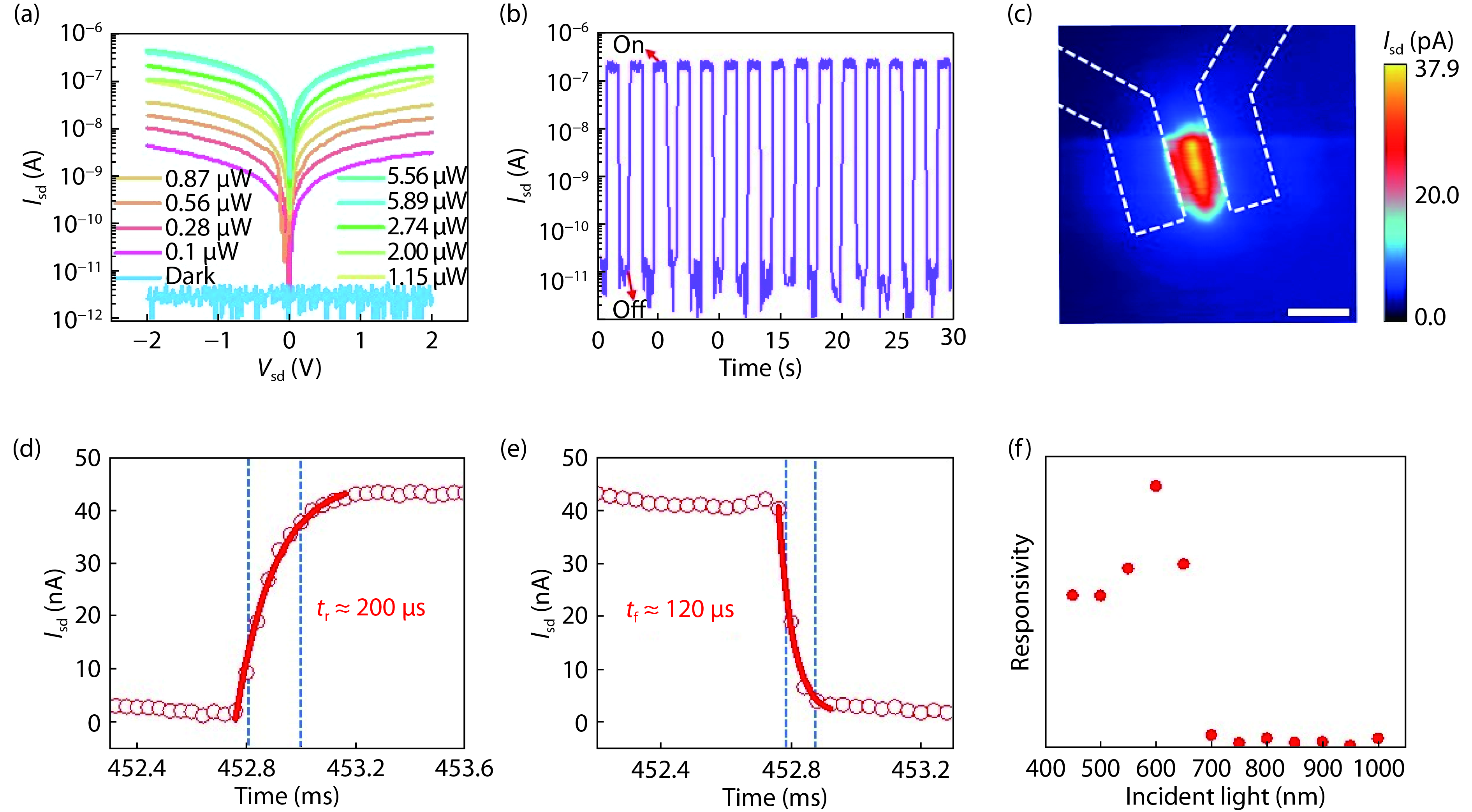
During the past decades, transition metal dichalcogenides (TMDs) have received special focus for their unique properties in photoelectric detection. As one important member of TMDs, MoS2 has been made into photodetector purely or combined with other materials, such as graphene, ionic liquid, and ferroelectric materials. Here, we report a gate-free MoS2 phototransistor combined with organic ferroelectric material poly(vinylidene fluoride-trifluoroethylene) (P(VDF-TrFE)). In this device, the remnant polarization field in P(VDF-TrFE) is obtained from the piezoelectric force microscope (PFM) probe with a positive or negative bias, which can turn the dipoles from disorder to be the same direction. Then, the MoS2 channel can be maintained at an accumulated state with downward polarization field modulation and a depleted state with upward polarization field modulation. Moreover, the P(VDF-TrFE) segregates MoS2 from oxygen and water molecules around surroundings, which enables a cleaner surface state. As a photodetector, an ultra-low dark current of 10–11 A, on/off ration of more than 104 and a fast photoresponse time of 120 μs are achieved. This work provides a new method to make high-performance phototransistors assisted by the ferroelectric domain which can operate without a gate electrode and demonstrates great potential for ultra-low power consumption applications.

J. Semicond.
2019, 40(9): 092101 doi: 10.1088/1674-4926/40/9/092101
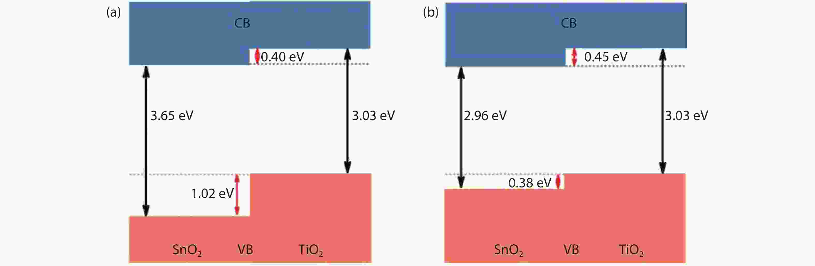
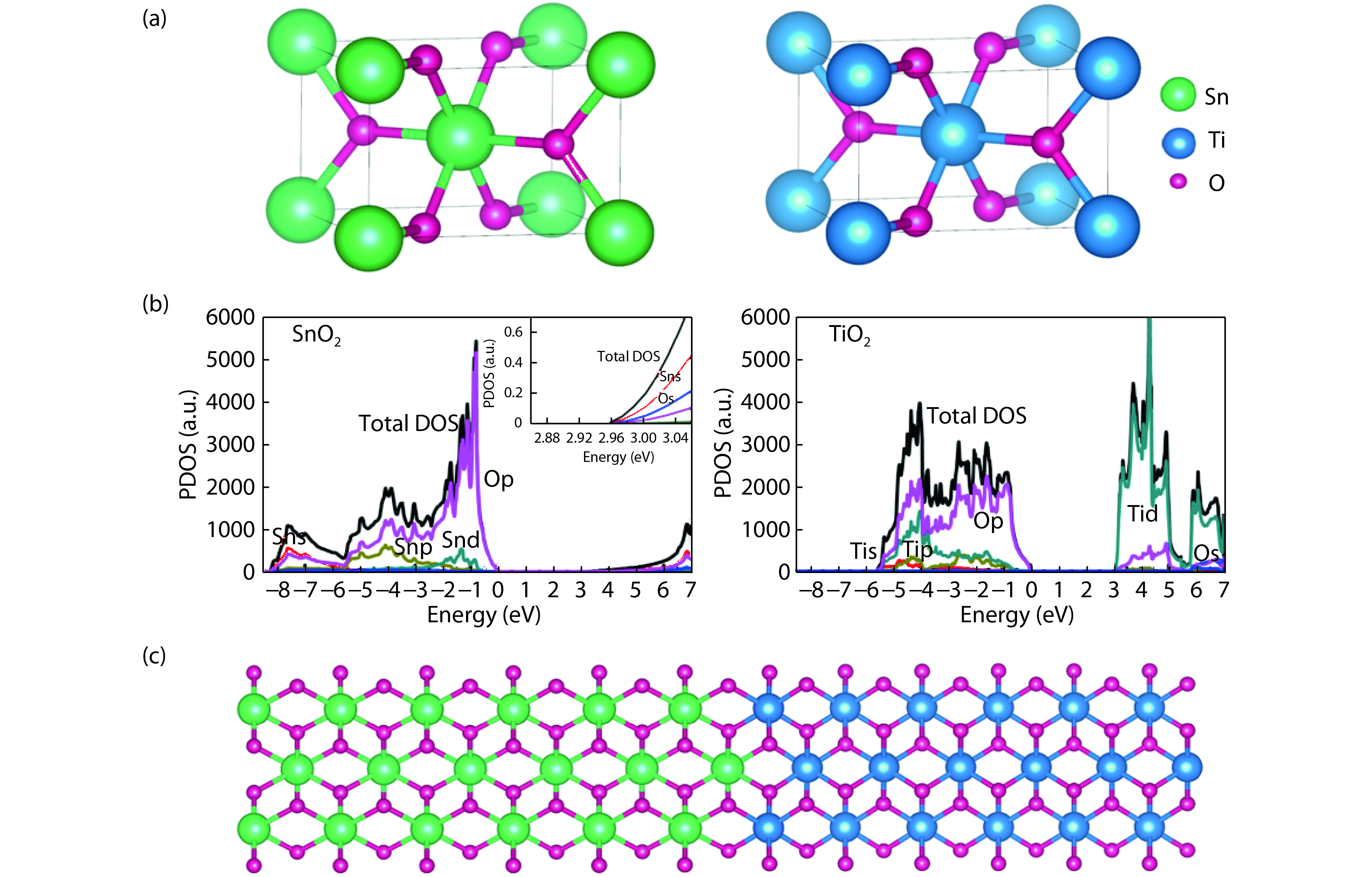
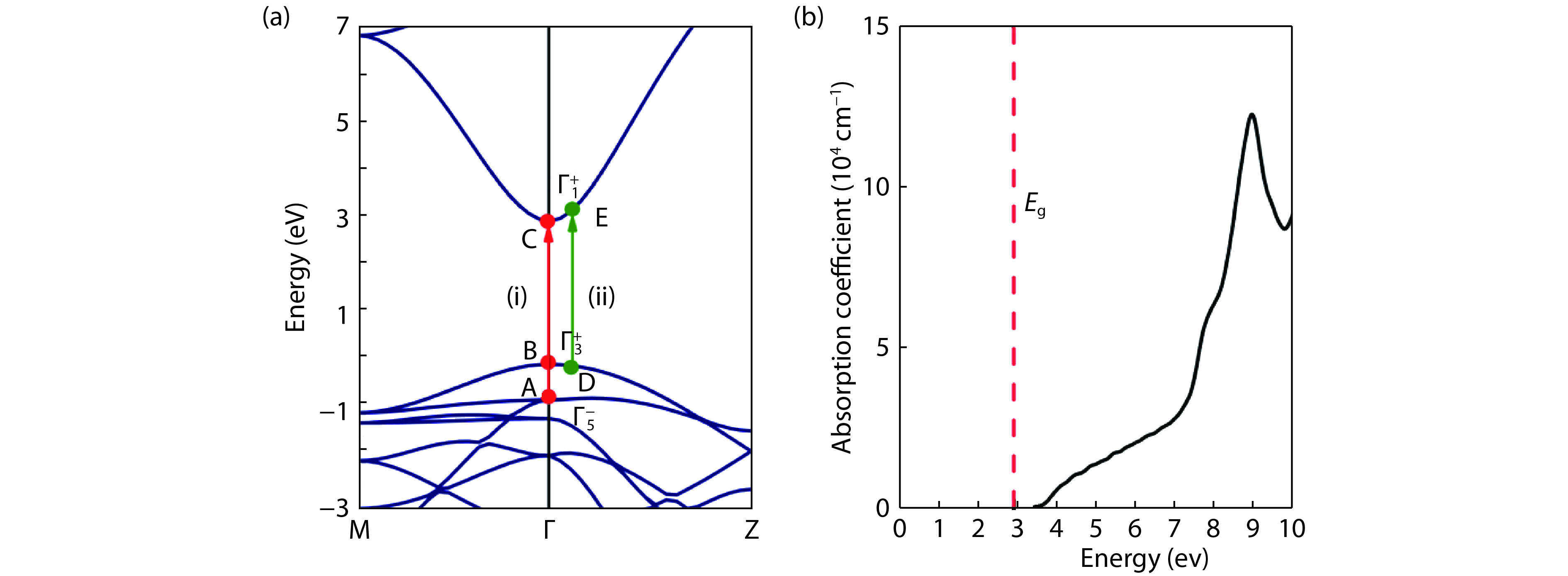
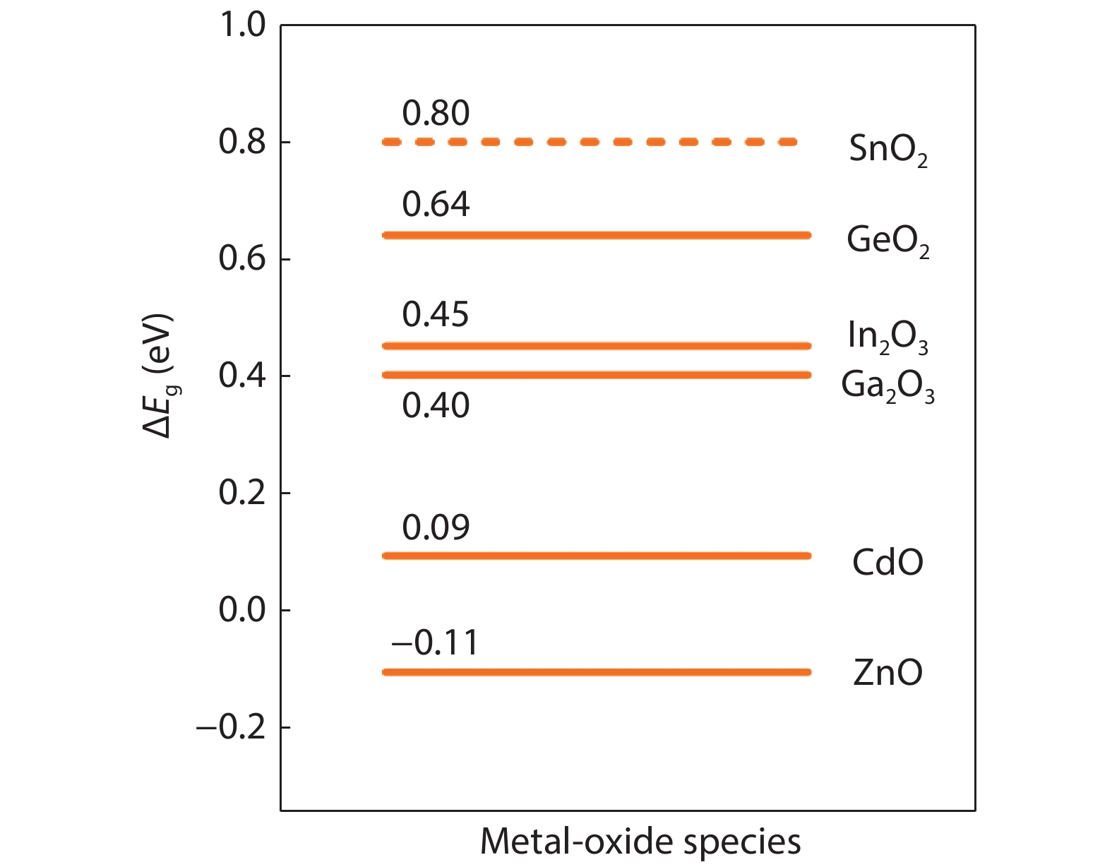
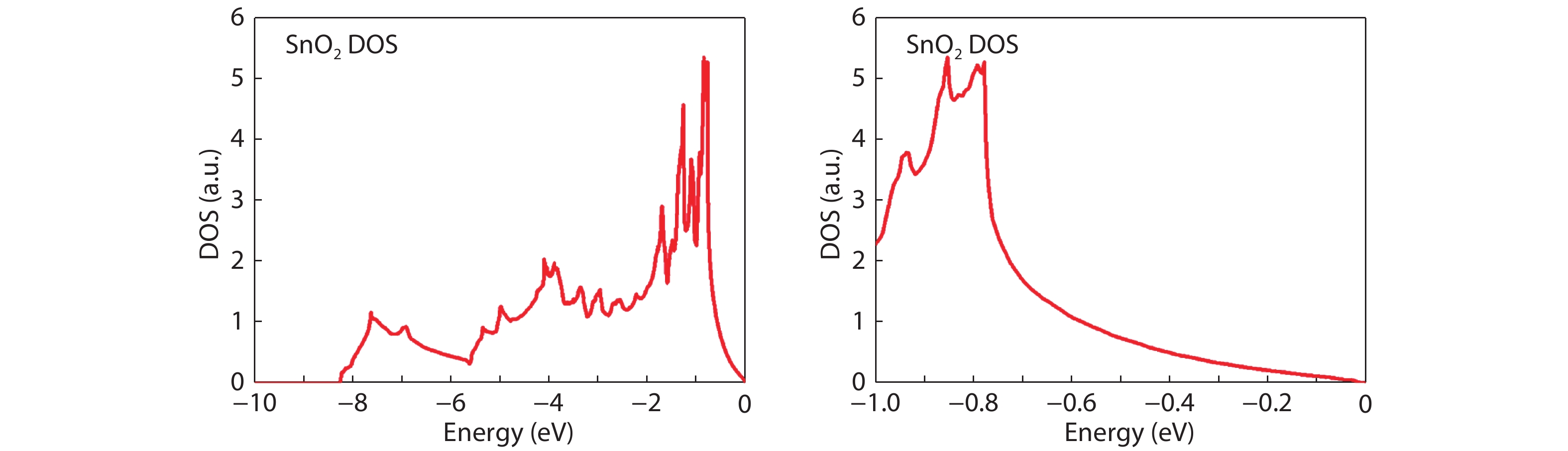
From the recent experimentally observed conduction band offset and previously reported band gaps, one may deduce that the valence band offset between rutile SnO2 and TiO2 is around 1 eV, with TiO2 having a higher valence band maximum. This implication sharply contradicts the fact that the two compounds have the same rutile structure and the Γ3+ VBM state is mostly an oxygen p state with a small amount of cation d character, thus one would expect that SnO2 and TiO2 should have small valence band offset. If the valence band offset between SnO2 and TiO2 is indeed small, one may question the correctness of the previously reported band gaps of SnO2 and TiO2. In this paper, using first-principles calculations with different levels of computational methods and functionals within the density functional theory, we reinvestigate the long-standing band gap problem for SnO2. Our analysis suggests that the fundamental band gap of SnO2 should be similar to that of TiO2, i.e., around 3.0 eV. This value is significantly smaller than the previously reported value of about 3.6 eV, which can be attributed as the optical band gap of this material. Similar to what has been found in In2O3, the discrepancy between the fundamental and optical gaps of SnO2 can be ascribed to the inversion symmetry of its crystal structure and the resultant dipole-forbidden transitions between its band edges. Our results are consistent with most of the optical and electrical measurements of the band gaps and band offset between SnO2 and TiO2, thus provide new understanding of the band structure and optical properties of SnO2. Experimental tests of our predictions are called for.

J. Semicond.
2019, 40(9): 092501 doi: 10.1088/1674-4926/40/9/092501
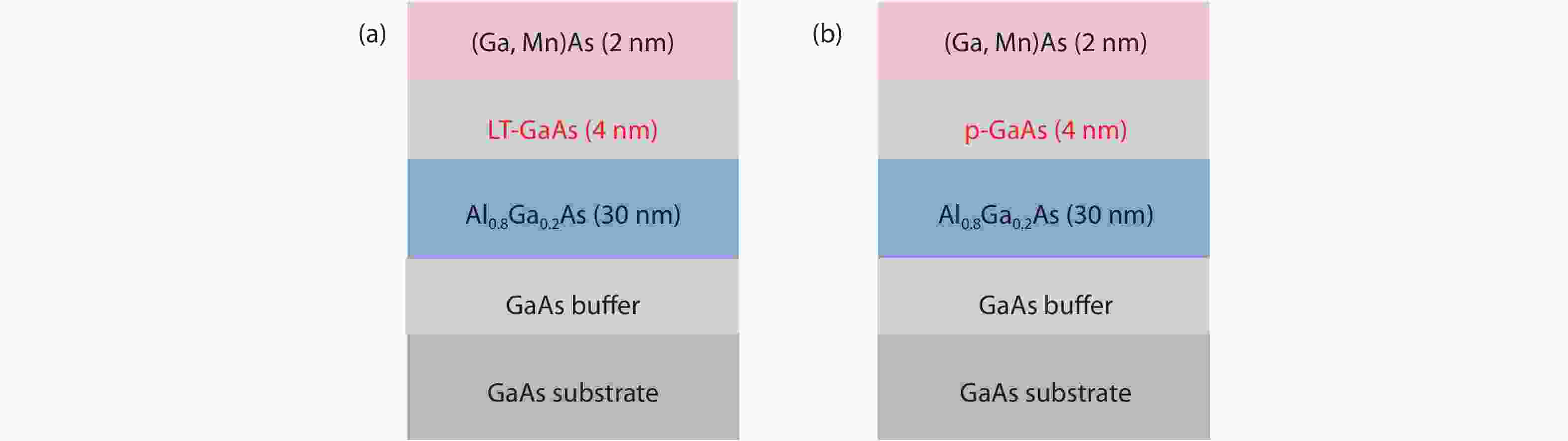
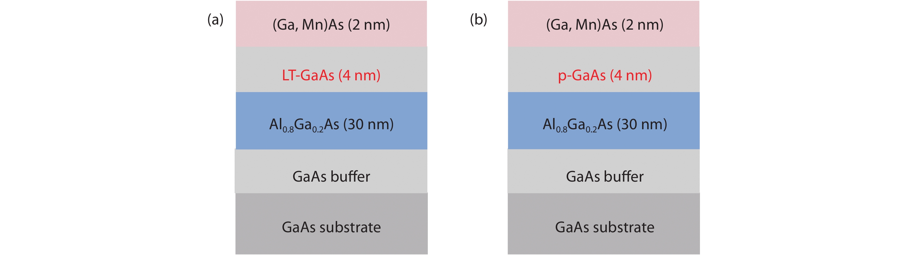
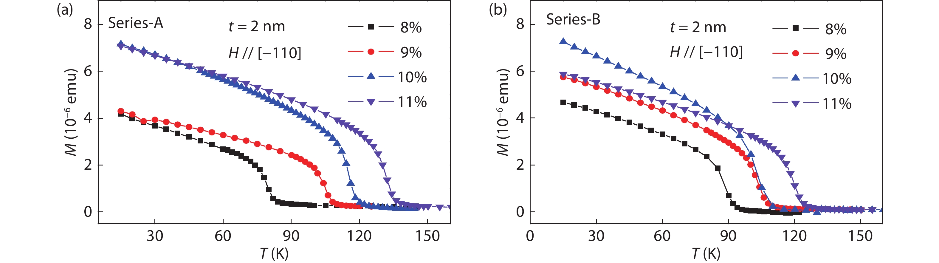
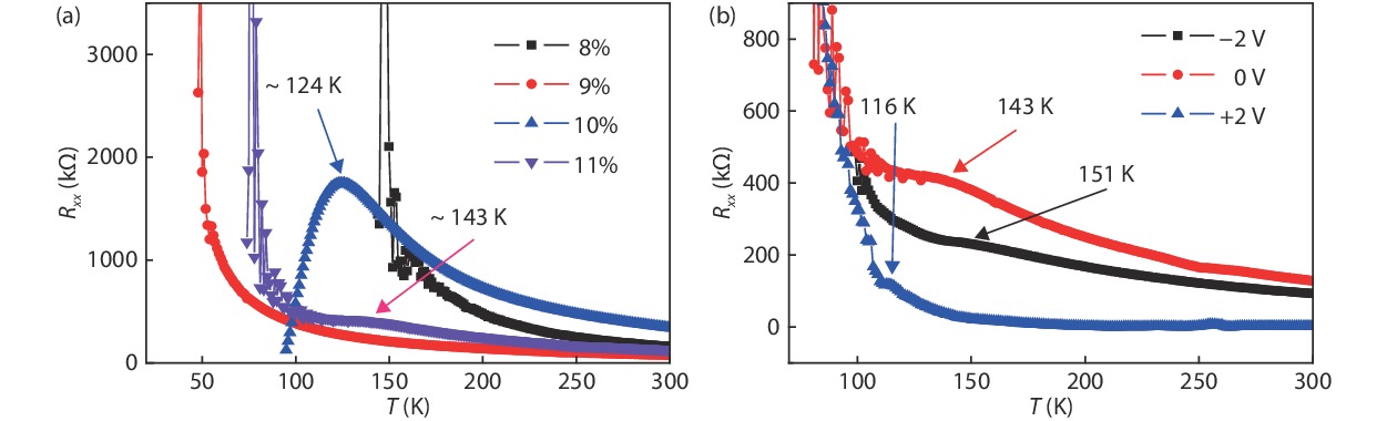
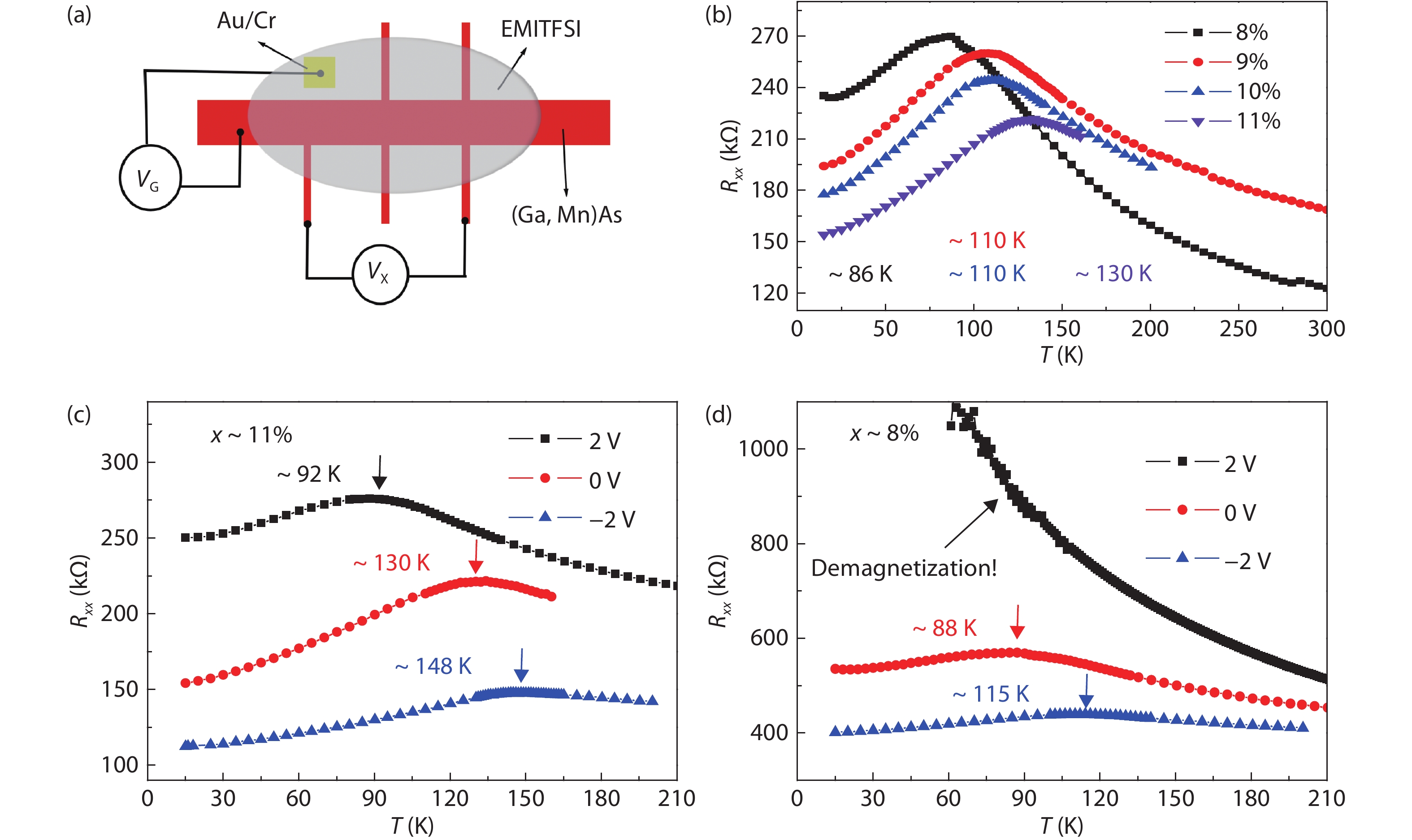
Taking the advantages of semiconducting properties and carrier-mediated ferromagnetism in (Ga,Mn)As, a giant modulation of magnetism via electric field in (Ga,Mn)As ultrathin film has been demonstrated. Specifically, huge interfacial electric field is obtained by using ionic liquid as the gate dielectric. Both magnetization and transport measurements are employed to characterize the samples, while the transport data are used to analyze the electric filed effect on magnetism. Complete demagnetization of (Ga,Mn)As film is then realized by thinning its thickness down to ~2 nm, during which the degradation of ferromagnetism of (Ga,Mn)As ultrathin film induced by quantum confinement effect is suppressed by inserting a heavily-doped p-type GaAs buffer layer. The variation of the Curie temperature is more than 100 K, which is nearly 5-times larger than previous results. Our results provide a new pathway on the efficient electrical control of magnetism.