Polycrystalline thin films of silver antimony selenide have been deposited using a reactive evaporation technique onto an ultrasonically cleaned glass substrate at a vacuum of 10-5 torr. The preparative parameters, like substrate temperature and incident fluxes, have been properly controlled in order to get stoichiometric, good quality and reproducible thin film samples. The samples are characterized by XRD, SEM, AFM and a UV-vis-NIR spectrophotometer. The prepared sample is found to be polycrystalline in nature. From the XRD pattern, the average particle size and lattice constant are calculated. The dislocation density, strain and number of crystallites per unit area are evaluated using the average particle size. The dependence of the electrical conductivity on the temperature has also been studied and the prepared AgSbSe2 samples are semiconducting in nature. The AgSbSe2 thin films exhibited an indirect allowed optical transition with a band gap of 0.64 eV. The compound exhibits promising thermoelectric properties, a large Seebeck coefficient of 30 mV/K at 48 K due to strong phonon electron interaction. It shows a strong temperature dependence on thermoelectric properties, including the inversion of a dominant carrier type from p to n over a low temperature range 9-300 K, which is explained on the basis of a phonon drag effect.
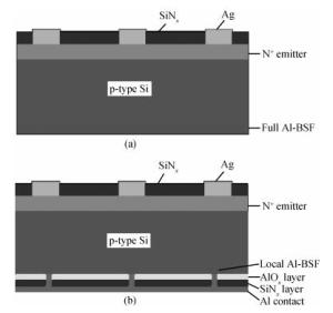
A stack of Al2O3/SiNx dual layer was applied for the back side surface passivation of p-type multi-crystalline silicon solar cells, with laser-opened line metal contacts, forming a local aluminum back surface field (local Al-BSF) structure. A slight amount of Al2O3, wrapping around to the front side of the wafer during the thermal atomic layer deposition process, was found to have a negative influence on cell performance. The different process flow was found to lead to a different cell performance, because of the Al2O3 wrapping around the front surface. The best cell performance, with an absolute efficiency gain of about 0.6% compared with the normal full Al-BSF structure solar cell, was achieved when the Al2O3 layer was deposited after the front surface of the wafer had been covered by a SiNx layer. We discuss the possible reasons for this phenomenon, and propose three explanations as the Ag paste, being hindered from firing through the front passivation layer, degraded the SiNx passivation effect and the Al2O3 induced an inversion effect on the front surface. Characterization methods like internal quantum efficiency and contact resistance scanning were used to assist our understanding of the underlying mechanisms.
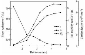
Cu and Cu/ITO films were prepared on polyethylene terephthalate (PET) substrates with a Ga2O3 buffer layer using radio frequency (RF) and direct current (DC) magnetron sputtering. The effect of Cu layer thickness on the optical and electrical properties of the Cu film deposited on a PET substrate with a Ga2O3 buffer layer was studied, and an appropriate Cu layer thickness of 4.2 nm was obtained. Changes in the optoelectrical properties of Cu(4.2 nm)/ITO(30 nm) films were investigated with respect to the Ga2O3 buffer layer thickness. The optical and electrical properties of the Cu/ITO films were significantly influenced by the thickness of the Ga2O3 buffer layer. A maximum transmission of 86%, sheet resistance of 45 Ω/□ and figure of merit of 3.96×10⁻³ Ω -1 were achieved for Cu(4.2 nm)/ITO(30 nm) films with a Ga2O3 layer thickness of 15 nm.

The oxidation induced stacking faults (OISFs) exposed on the surface of polished silicon substrate are harmful to the electrical performance and reliability of the device region located on the wafer surface. This work investigates the characteristics of the novel nano colloidal silica alkaline slurry, including polyamine and complex non-ions surface surfactant. The experimental results show that when the pH value is higher than 10.1, the removal rate can be higher than 750 nm/min and the surface roughness can be lower than 0.3 nm (10×10 μm2). The surface OISFs existing on the wafer are efficiently controlled with the slurry, and the defect density on the polished wafer surface decreases greatly as well.
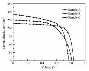
This paper presents the temperature dependence measurements characterisation of several InAs/GaAs quantum dots (QDs) solar cell devices. The devices with cylindrical geometry were fabricated and characterised on-wafer under 20 suns in a temperature range from 300°K to 430°K. The temperature dependence parameters such as open circuit voltage, short circuit density current, fill factor and efficiency are studied in detail. The increase of temperature produces an enhancement of the short circuit current. However, the open circuit voltage is degraded because the temperature increases the recombination phenomena involved, as well as reducing the effective band gap of the semiconductor.
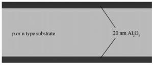
Atom layer deposition (ALD)-Al2O3 thin films are considered effective passivation layers for p-type silicon surfaces. A lower surface recombination rate was obtained through optimizing the deposition parameters. The effects of some of the basic substrate characteristics including material type, bulk resistivity and surface morphology on the passivation performance of ALD-Al2O3 are evaluated in this paper. Surface recombination velocities of 7.8 cm/s and 6.5 cm/s were obtained for p-type and n-type wafers without emitters, respectively. Substrates with bulk resistivity ranging from 1.5 to 4 Ω · cm were all great for such passivation films, and a higher implied Voc of 660 mV on the 3 Ω · cm substrate was achieved. A minority carrier lifetime (MCL) of nearly 10 μs higher was obtained for cells with a polished back surface compared to those with a textured surface, which indicates the necessity of the polishing process for high-efficiency solar cells. For n-type semi-finished solar cells, a lower effective front surface recombination velocity of 31.8 cm/s was acquired, implying the great potential of (ALD)-Al2O3 thin films for high-efficiency n-type solar cells.
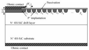
This paper presents the design and fabrication of an effective, robust and process-tolerant floating guard ring termination on high voltage 4H-SiC PiN diodes. Different design factors were studied by numerical simulations and evaluated by device fabrication and measurement. The device fabrication was based on a 12 μm thick drift layer with an N-type doping concentration of 8×1015 cm-3. P+ regions in the termination structure and anode layer were formed by multiple aluminum implantations. The fabricated devices present a highest breakdown voltage of 1.4 kV, which is higher than the simulated value. For the fabricated 15 diodes in one chip, all of them exceeded the breakdown voltage of 1 kV and six of them reached the desired breakdown value of 1.2 kV.
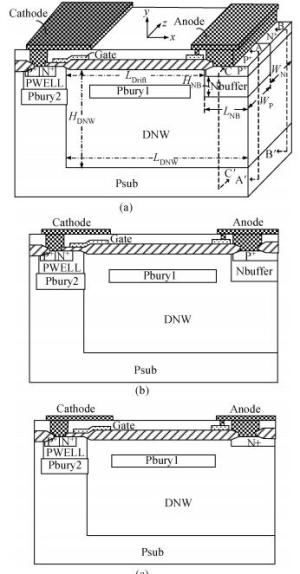
A dual conduction paths segmented anode lateral insulated-gate bipolar transistor (DSA-LIGBT) which uses triple reduced surface field (RESURF) technology is proposed. Due to the hybrid structures of triple RESURF LDMOS (T-LDMOS) and traditional LIGBT, firstly, a wide p-type anode is beneficial to the small shift voltage (VST) and low specific on-resistance (Ron, sp) when the anode voltage (VA) is larger than VST. Secondly, a wide n-type anode and triple RESURF technology are used to get a low Ron, sp when VA is less than VST. Meanwhile, it can accelerate the extraction of electrons, which brings a low turn-off time (Toff). Experimental results show that:VST is only 0.9 V, Ron, sp (Ron×Area) are 11.7 and 3.6 Ω · mm2 when anode voltage VA equals 0.9 and 3 V, respectively, the breakdown voltage reaches to 800 V and Toff is only 450 ns.
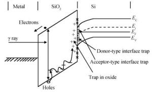
Using positive surface charge instead of traditional γ-ray total dose irradiation, the electric field distribution of a P-channel VDMOS terminal has been analyzed. A novel terminal structure for improving the total dose irradiation hardened of P-channel VDMOS has been proposed, and the structure is simulated and demonstrated with a -150 V P-channel VDMOS. The results show that the peak current density is reduced from 5.51×10³ A/cm2 to 2.01×10³ A/cm2, and the changed value of the breakdown voltage is 2.5 V at 500 krad(Si). Especially, using 60Co and X-ray to validate the results, which strictly match with the simulated values, there is not any added mask or process to fabricate the novel structure, of which the process is compatible with common P-channel VDMOS processes. The novel terminal structure can be widely used in total irradiation hardened P-channel VDMOS design and fabrication, which holds a great potential application in the space irradiation environment.
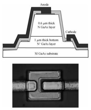
A GaAs-based planar Schottky varactor diode (PSVD) is successfully developed to meet the demand of millimeter-wave harmonic generation. Based on the measured S-parameter, I-V and C-V characteristics, an accurate and reliable extraction method of the millimeter-wave large signal equivalent circuit model of the PSVD is proposed and used to extract the model parameters of two PSVDs with Schottky contact areas of 160 μm2 and 49 μm2, respectively. The simulated S-parameter, I-V and C-V performances of the proposed physics-based model are in good agreement with the measured one over the frequency range from 0.1 to 40 GHz for wide operation bias range from -10 to 0.6 V for these two PSVDs. The proposed equivalent large signal circuit model of this PSVD has been proven to be reliable and can potentially be used to design microwave circuits.
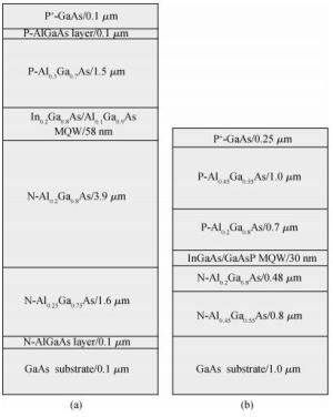
To obtain a high-power and efficient single-mode laser, a new laser called the slab coupled optical waveguide laser (SCOWL) has been developed. We have simulated its structure and grown the chip with this structure by low-pressure metal organic chemical vapor deposition. We have also produced the broad-area SCOWL and compared it with the traditional structure laser in terms of some performances. This work lays the foundation for further research of ridged lasers with the same structure.

A simple and cost-effective remodulation scheme using a two-section reflective semiconductor optical amplifier (RSOA) is proposed for a colorless optical network unit (ONU). Under proper injection currents, the front section functions as a modulator to upload the upstream signal while the rear section serves as a data eraser for efficient suppression of the downstream data. The dependences of the upstream transmission performance on the lengths and driven currents of the RSOA, the injection optical power and extinction ratio of the downstream are investigated. By optimizing these parameters, the downstream data can be more completely suppressed and the upstream transmission performance can be greatly improved.
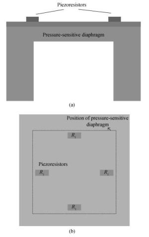
A novel algorithmic method, based on the different stress distribution on the surface of thin film in an SOI microstructure, is put forward to calculate the value of the silicon piezoresistance on the sensitive film. In the proposed method, we take the Ritz method as an initial theoretical model to calculate the rate of piezoresistance Δ R/R through an integral (the closed area Ω where the surface piezoresistance of the film lies as the integral area and the product of stress σ and piezoresistive coefficient π as the integral object) and compare the theoretical values with the experimental results. Compared with the traditional method, this novel calculation method is more accurate when applied to calculating the value of the silicon piezoresistance on the sensitive film of an SOI pieoresistive pressure sensor.
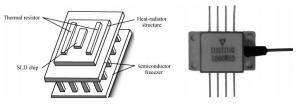
Light source modules are the most crucial and fragile devices that affect the life and reliability of the interferometric fiber optic gyroscope (IFOG). While the light emitting chips were stable in most cases, the module packaging proved to be less satisfactory. In long-term storage or the working environment, the ambient temperature changes constantly and thus the packaging and coupling performance of light source modules are more likely to degrade slowly due to different materials with different coefficients of thermal expansion in the bonding interface. A constant temperature accelerated life test cannot evaluate the impact of temperature variation on the performance of a module package, so the temperature cycling accelerated life test was studied. The main failure mechanism affecting light source modules is package failure due to solder fatigue failure including a fiber coupling shift, loss of cooling efficiency and thermal resistor degradation, so the Norris-Landzberg model was used to model solder fatigue life and determine the activation energy related to solder fatigue failure mechanism. By analyzing the test data, activation energy was determined and then the mean life of light source modules in different storage environments with a continuously changing temperature was simulated, which has provided direct reference data for the storage life prediction of IFOG.

The performance of high density chips operating in the GHz range is mostly affected by on-chip interconnects. The interconnect delay depends on many factors, a few of them are inputs toggling patterns, line & coupling parasitics, input rise/fall time and source/load characteristics. The transition time of the input is of prime importance in high speed circuits. This paper addresses the FDTD based analysis of transition time effects on functional and dynamic crosstalk. The analysis is carried out for equal and unequal transition times of coupled inputs. The analysis of the effects of unequal rise time is equally important because practically, it is quite common to have mismatching in the rise time of the signals transmitting through different length wires. To demonstrate the effects, two distributed RLC lines coupled inductively and capacitively are taken into consideration. The FDTD technique is used because it gives accurate results and carries time domain analysis of coupled lines. The number of lumps in SPICE simulations is considered the same as those of spatial segments. To validate the FDTD computed results, SPICE simulations are run and results are compared. A good agreement of the computed results has been observed with respect to SPICE simulated results. An average error of less than 3.2% is observed in the computation of the performance parameters using the proposed method.

A low power 20 GHz CMOS dynamic latched regeneration comparator for ultra-high-speed, low-power analog-to-digital converters (ADCs) is proposed. The time constant in both the tracking and regeneration phases of the latch are analyzed based on the small signal model. A dynamic source-common logic (SCL) topology is adopted in the master-slave latch to increase the tracking and regeneration speeds. Implemented in 90 nm CMOS technology, this comparator only occupies a die area of 65×150 μm2 with a power dissipation of 14 mW from a 1.2 V power supply. The measurement results show that the comparator can work up to 20 GHz. Operating with an input frequency of 1 GHz, the circuit can oversample up to 20 Giga-sampling-per-second (GSps) with 5 bits resolution; while operating at Nyquist, the comparator can sample up to 20 GSps with 4 bits resolution. The comparator has been successfully used in a 20 GSps flash ADC and the circuit can be also used in other high speed applications.

A double chopper-stabilized analog front-end (DCS-AFE) circuit for a thermopile sensor is presented, which includes a closed-loop front-end amplifier and a 2nd-order 1 bit quantization sigma-delta modulator. The amplifier with a closed-loop structure ensures the gain stability against the temperature. Moreover, by adopting the chopper-stabilized technique both for the amplifier and 2nd-order 1-bit quantization sigma-delta modulator, the low-frequency 1/f noise and offset is reduced and high resolution is achieved. The AFE is implemented in the SMIC 0.18 μm 1P6M CMOS process. The measurement results show that in a 3.3 V power supply, 1 Hz input frequency and 3KHz clock frequency, the peak signal-to-noise and distortion ratio (SNDR) is 55.4 dB, the effective number of bits (ENOB) is 8.92 bit, and in the range of -20 to 85 degrees, the detection resolution is 0.2 degree.
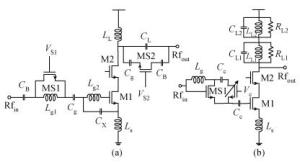
A reconfigurable dual-band LNA is presented. The LNA employs switching capacitors and circuit in to realize the dual-band operation. These methodologies are used to design and implement a reconfigurable LNA for IMT-A and UWB application. The LNA is implemented using TSMC-0.13 μm CMOS technology. Measured performance shows an input matching of better than -13.5 dB, a voltage gain of 18-22.8 dB, with an NF of 4.3-4.7 dB in the band of 3.4-3.6 GHz, and an input matching of better than -9.7 dB, a voltage gain of 14.7-22.4 dB, and with an NF of 3.7-4.9 dB in the band of 4.2-4.8 GHz. According to the measure results, the proposed LNA achieves dual-band operation, and it proves the feasibility of the proposed topology.
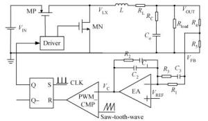
A high switching frequency voltage-mode buck converter with fast voltage-tracking speed and wide output voltage range has been proposed. A novel error amplifier (EA) is presented to achieve a high DC gain and get high phase margin, including a resistor and capacitor net, a unit gain block and a high gain block. The investigated converter has been fabricated with GF 0.35 μm CMOS process and can operate at 6 MHz with the output voltage range from 0.6 to 3.4 V. The experimental results show that the voltage-tracking speed can achieve 8.8 μs/V for up-tracking and 6 μs/V for down-tracking. Besides, the recovery time is less than 8 μs while the load current suddenly changes 400 mA.

This paper presents a 0.6 V 10 bit successive approximation register (SAR) ADC design dedicated to the wireless sensor network application. It adopts a monotonic switching scheme in the DAC to save chip area and power consumption. The main drawback of the monotonic switching scheme is its large common mode shift and the associated comparator offset variation. Due to the limited headroom at the 0.6 V supply voltage, the conventional constant current biasing technique cannot be applied to the dynamic comparator. In this design, a common mode stabilizer is introduced to address this issue in low-voltage design. The effectiveness of this method is verified through both simulation and measurement results. Fabricated with 1P8M 0.13 μm CMOS technology, the proposed SAR ADC consumes 6.3 μW at 1 MS/s from a 0.6 V supply, and achieves 51.25 dB SNDR at the Nyquist frequency and FOM of 21 fJ/conversion-step. The core area is only 120×300 μm2.
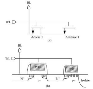
A 4-kbit low-cost one-time programmable (OTP) memory macro for embedded applications is designed and implemented in a 0.18-μm standard CMOS process. The area of the proposed 1.5 transistor (1.5T) OTP cell is 2.13 μm2, which is a 49.3% size reduction compared to the previously reported cells. The 1.5T cell is fabricated and measured and shows a large programming window without any disturbance. A novel high voltage switch (HVSW) circuit is also proposed to make sure the OTP macro, implemented in a standard CMOS process, works reliably with the high program voltage. The OTP macro is embedded in negative radio frequency identification (RFID) tags. The full chip size, including the analog front-end, digital controller and the 4-kbit OTP macro, is 600×600 μm2. The 4-kbit OTP macro only consumes 200×260 μm2. The measurement shows a 100% program yield by adjusting the program time and has obvious advantages in the core area and power consumption compared to the reported 3T and 2T OTP cores.
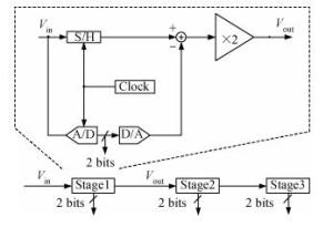
A novel fully differential high speed high resolution low offset CMOS dynamic comparator has been implemented in the SMIC 0.18 μm process used for a sample-and-hold amplifier (SHA)-less pipelined analog-to-digital converters (ADC). Based on the analysis and optimization between delay time and offset, an enhanced reset architecture with transmission gate was introduced to speed up the comparison and reset procedure. Four inputs with two cross coupled differential pairs, reconstituted bias circuit for tail current transistor and common centroid layouts make the comparator more robust against mismatch and process variations. The simulation results demonstrate that the proposed design achieves 1 mV sensitivity at 2.2 GHz sampling rate with a power consumption of 510 μW, while the mean offset voltage is equal to 10.244 mV.
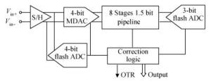
A high performance sample-and-hold (S/H) circuit used in a pipelined analog-to-digital converter (ADC) is presented. Capacitor flip-around architecture is used in this S/H circuit with a novel gain-boosted differential folded cascode operational transconductance amplifier. A double-bootstrapped switch is designed to improve the performance of the circuit. The circuit is implemented using a 0.18 μm 1P6M CMOS process. Measurement results show that the effective number of bits is 14.03 bits, the spurious free dynamic range is 94.62 dB, the signal to noise and distortion ratio is 86.28 dB, and the total harmonic distortion is -91.84 dB for a 5 MHz input signal with 50 MS/s sampling rate. A pipeline ADC with the designed S/H circuit has been implemented.
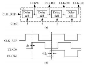
A multimode DLL with trade-off between multiphase and static phase error is presented. By adopting a multimode control circuit to regroup the delay line, a better static phase error performance can be achieved while reducing the number of output phases. The DLL accomplishes three operation modes:mode1 with a four-phase output, mode2 with a two-phase output and a better static phase error performance, and mode3 with only a one-phase output but the best static phase error performance. The proposed DLL has been fabricated in 0.13 μm CMOS technology and measurement results show that the static phase errors of mode1, mode2 and mode3 are -18.2 ps, 11.8 ps and -6.44 ps, respectively, at 200 MHz. The measured RMS and peak-to-peak jitters of mode1, mode2 and mode3 are 2.0 ps, 2.2 ps, 2.1 ps and 10 ps, 9.3 ps, 10 ps respectively.
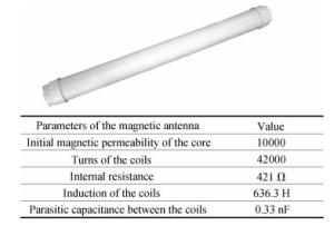
Calibrating the super low frequency (SLF) magnetic antenna in magnetic free space or an outdoor environment is difficult and complicated due to the large size calibration instruments and lots of measurement times. Aiming to calibrate the SLF magnetic antenna simply and efficiently, a calibration system comprised of a multi-frequency source, an A.C constant-current source and a solenoid is proposed according to the characteristic of an SLF magnetic antenna. The static magnetic transfer coefficient of the designed solenoid is calibrated. The measurement of the frequency response characteristics suggests the transfer coefficient remains unchanged in the range of the SLF band and is unaffected by the magnetic antenna internally installed. The CORDIC algorithm implemented in an FPGA is realized to generate a linear evenly-spaced multi-frequency signal with equal energy at each frequency. An A.C constant weak current source circuit is designed in order to avoid the impact on the magnetic induction intensity of a calibration system affected by impedance variation when frequency changing, linearity and the precision of the source are measured. The frequency characteristic of a magnetic antenna calibrated by the proposed calibration system agrees with the theoretical result and the standard Glass ring calibration result. The calibration precision satisfies the experimental requirement.
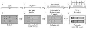
Superior graphene-metal contacts can improve the performance of graphene devices. We report on an experimental demonstration of Ge/Au/Ni/Au-based ohmic contact on graphene. The transfer length method (TLM) is adopted to measure the resistivity of graphene-metal contacts. We designed a process flow, which can avoid residual photoresist at the interface of metal and graphene. Additionally, rapid thermal annealing (RTA) at different temperatures as a post-processing method is studied to improve graphene-metal contact. The results reveal that the contact resistivity of graphene and Ge/Au/Ni/Au can reach 10-5 Ω· cm2 after RTA, and that 350℃ is optimum annealing temperature for the contact of graphene-Ge/Au/Ni/Au. This paper provides guidance for fabrication and applications of graphene devices.


