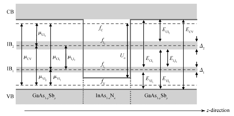
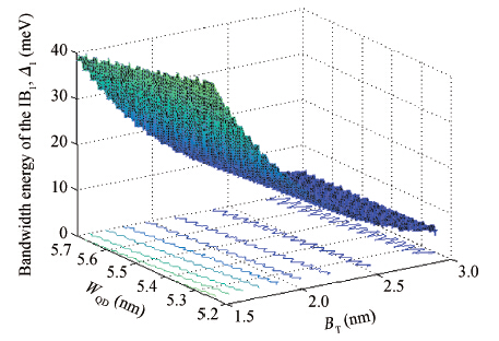
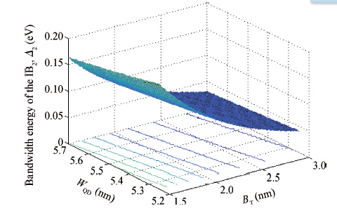
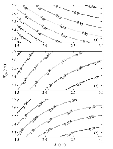
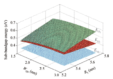
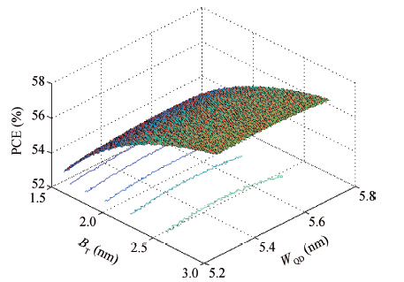
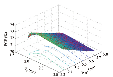
A mathematical model of quantum dot intermediate band solar cells (QDIBSCs) is investigated using two intermediate bands (IBs). These two IBs arise from the quantum dot (QD) semiconductor material within the bandgap energy. Some parameters such as the width of the QD (WQD) and the barrier thickness or the inter-dot distances between the QDs (BT) are studied to show their influence on the performance of the QDIBSC. The time-independent Schrödinger equation, which is solved using the Kronig-Penney model, is used to determine the position and bandwidth energies of the two IBs. In our proposed model, the cubic shape of the QDs from InAs0.9N0.1 and the barrier or host semiconductor material from GaAs0.98Sb0.02 are utilized. It is shown from the results obtained that changing the parameters WQD and BT has more influence on the bandwidth energy for the first IB, Δ1, than in the case of the second IB, Δ2. The optimum power conversion efficiencies (PCEs) of the QDIBSCs with two IBs for the model under study are 58.01% and 73.55% at 1 Sun and maximum solar concentration, respectively. One can observe that, in the case of the two IBs, an improvement of the PCE is achieved.

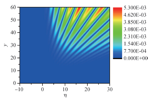
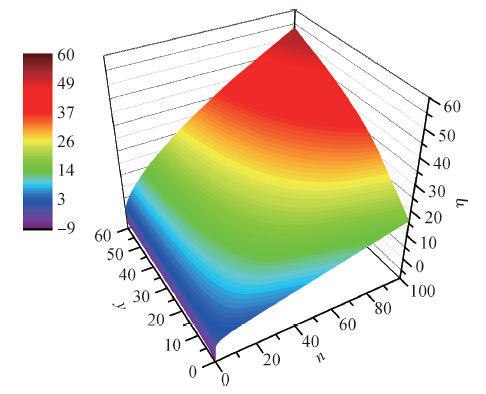
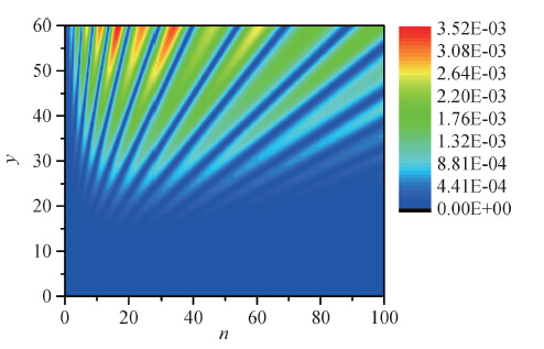
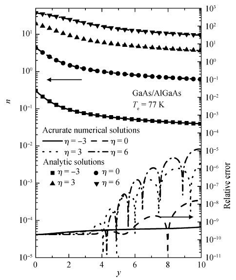
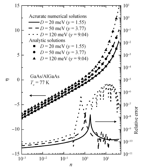
Analytical formulas for evaluating the relation of carrier density and Fermi energy for semiconductors with a tight-binding band have been proposed. The series expansions for a carrier density with fast convergency have been obtained by means of a Bessel function. A simple and analytical formula for Fermi energy has been derived with the help of the Gauss integration method. The results of the proposed formulas are in good agreement with accurate numerical solutions. The formulas have been successfully used in the calculation of carrier density and Fermi energy in a miniband superlattice system. Their accuracy is in the order of 10-5.

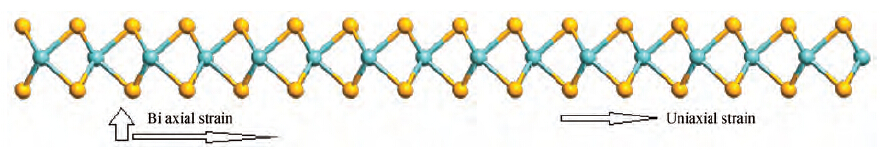
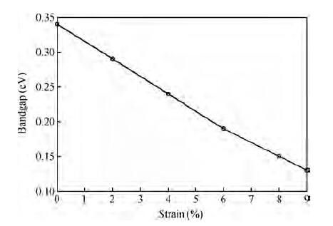
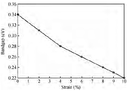
We have studied the electronic properties of molybdenum diselenide (MoSe2) in both bulk and monolayer (zigzag and armchair) forms using density function theory. The metallic nature of the zigzag MoSe2 (ZMoSe2) nanoribbon and the semiconducting behavior of the armchair MoSe2 (AMoSe2) nanoribbon have been explored using a band structure calculated using self-consistent calculations. We have also studied the variation in the bandgap in the presence of a small amount of strain (uniaxial, biaxial). The effect of tensile strain has been investigated and shifts in the conduction band and valance band have been observed with different amounts of applied strain.

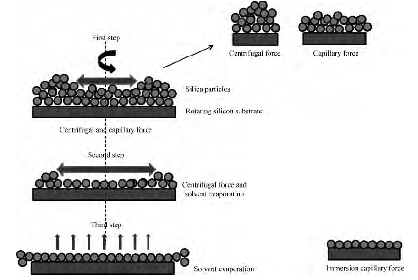
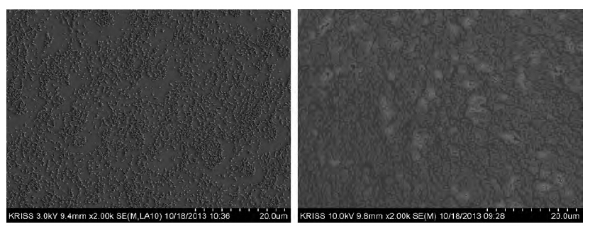
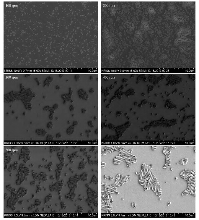
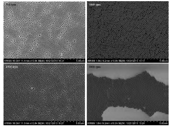
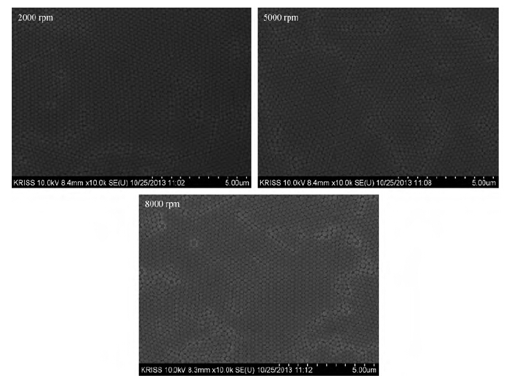
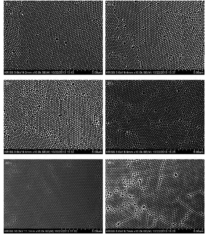
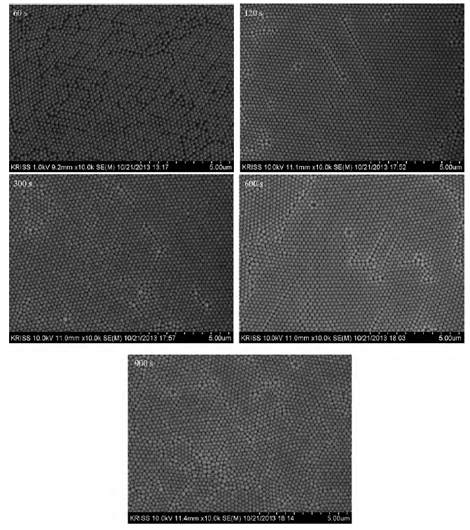
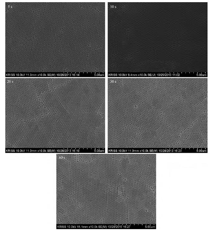
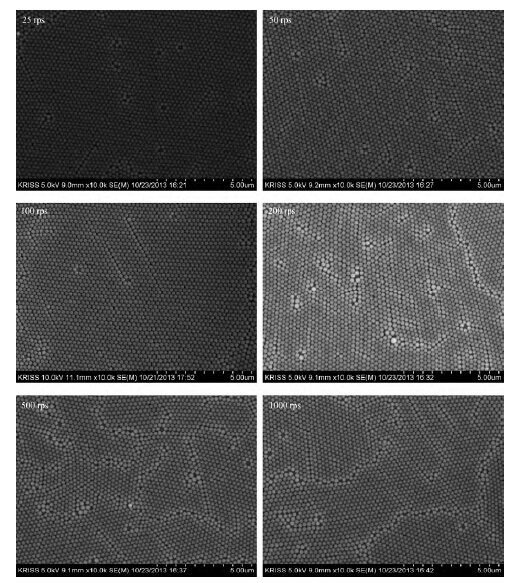
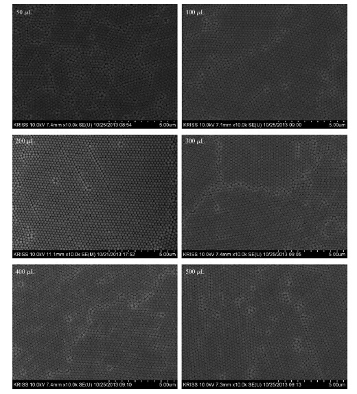
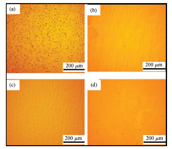
The highly ordered monolayer of submicron size silica (SiO2) particles (235 nm) is developed on p-silicon by using three-step spin-coating in colloidal suspension, which has significant potential in various applications. The influence of three-step spin speeds, spinning time, acceleration time between different steps, concentration of SiO2 particles in the solution, solution quantity, and the ambient humidity (relative humidity) on the properties of monolayer SiO2 are studied in order to achieve a large area monolayer film. A relatively high surface coverage and uniform monolayer film of SiO2 particles in the range of 85%-90% are achieved by appropriate control of the preparative parameters. We conclude that this method can be useful in industrial applications, because of the fabrication speed, surface coverage and cost of the process.
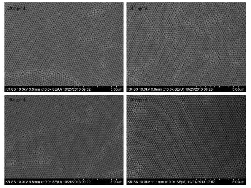

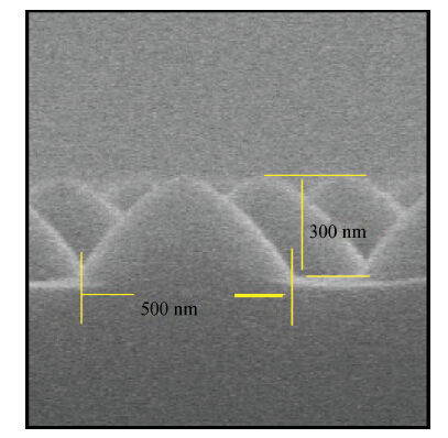
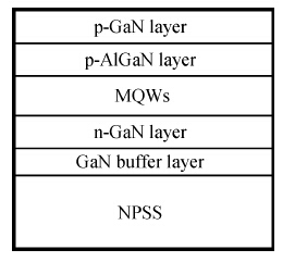
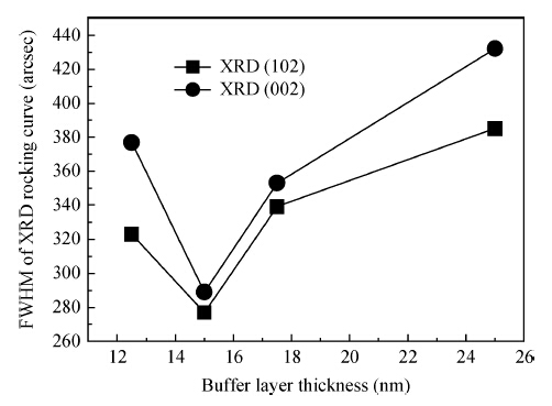
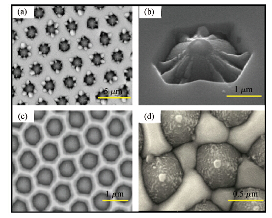
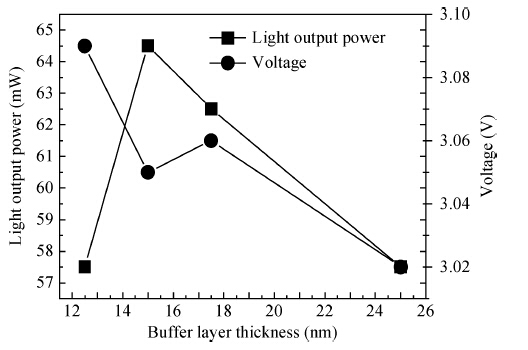
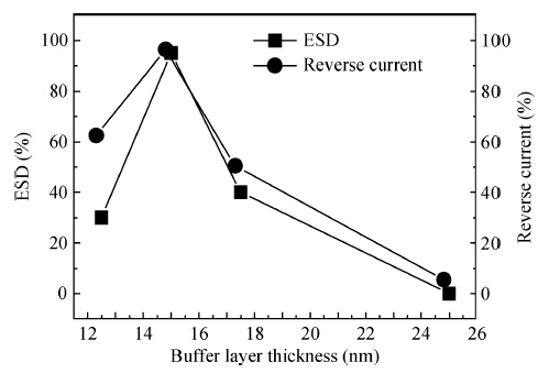
High-quality gallium nitride (GaN) film was grown on nano-patterned sapphire substrates (NPSS) and investigated using XRD and SEM. It was found that the optimum thickness of the GaN buffer layer on the NPSS is 15 nm, which is thinner than that on micro-patterned sapphire substrates (MPSS). An interesting phenomenon was observed for GaN film grown on NPSS:GaN mainly grows on the trench regions and little grows on the sidewalls of the patterns at the initial growth stage, which is dramatically different from GaN grown on MPSS. In addition, the electrical and optical properties of LEDs grown on NPSS were characterized.

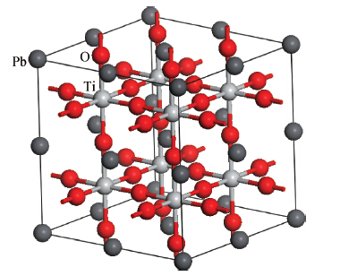
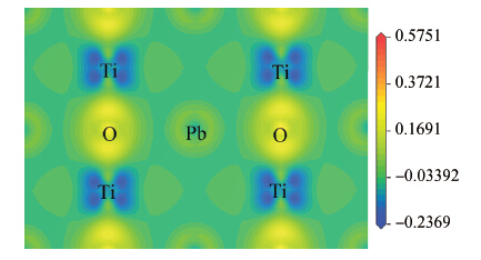
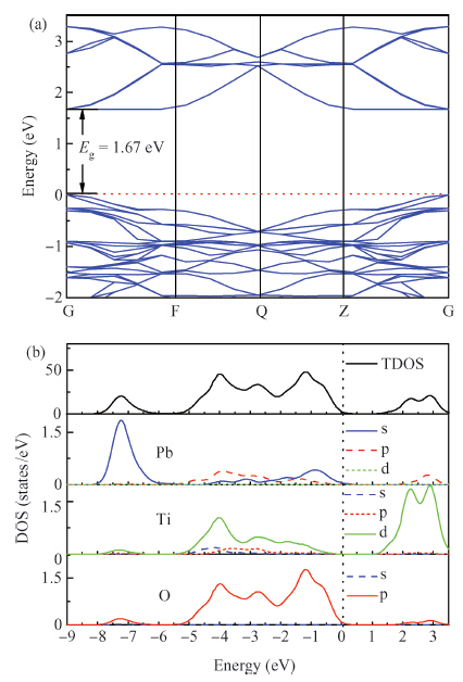
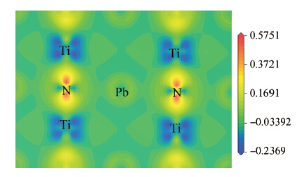
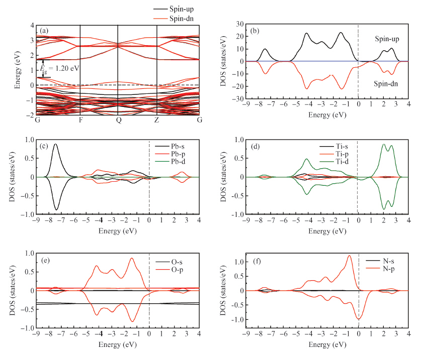
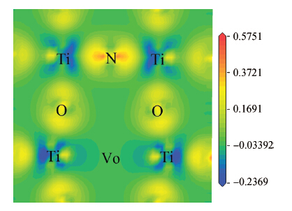
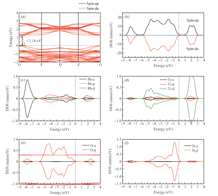
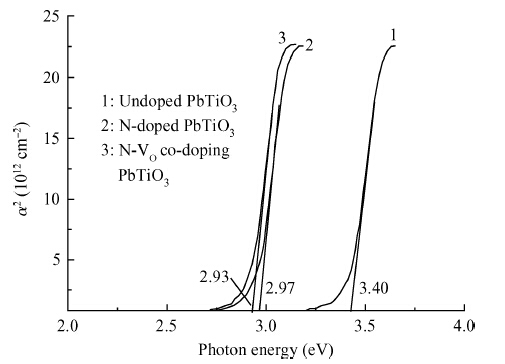
By using spin-polarized density functional theory calculations, the electron density differences, band structures and density of states of p-type N-doped PbTiO3 have been studied. In addition, the oxygen vacancy in N-doped PbTiO3 is also discussed. After the nitrogen dopant is introduced into the crystal, the N-doped PbTiO3 system is spin-polarized, the spin-down valance bands move to a high energy level and the Fermi energy level moves to the top of the valance bands, finally the band gap is narrowed. In this process, the N-doped PbTiO3 shows typical p-type semiconductor characteristics. When an oxygen vacancy and N impurity coexist in PbTiO3, there is no spin-polarized phenomenon. The conduction bands move downward and the acceptors are found to be fully compensated. The calculation results are mostly consistent with the experimental data.

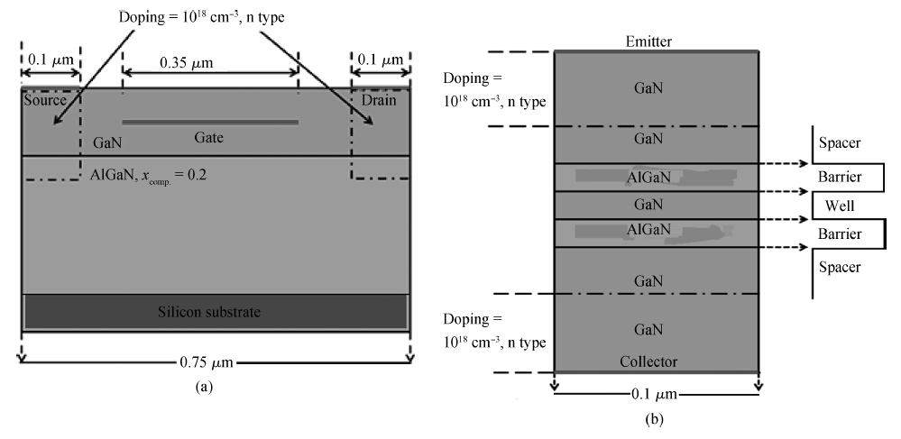
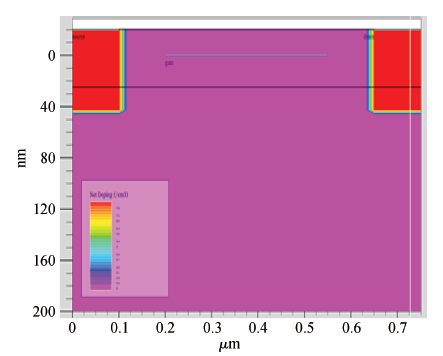
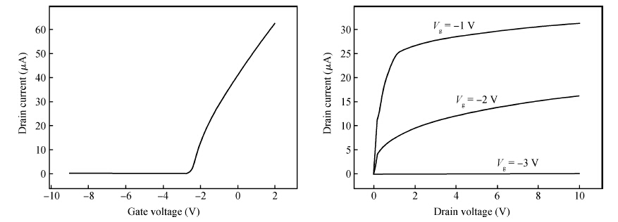
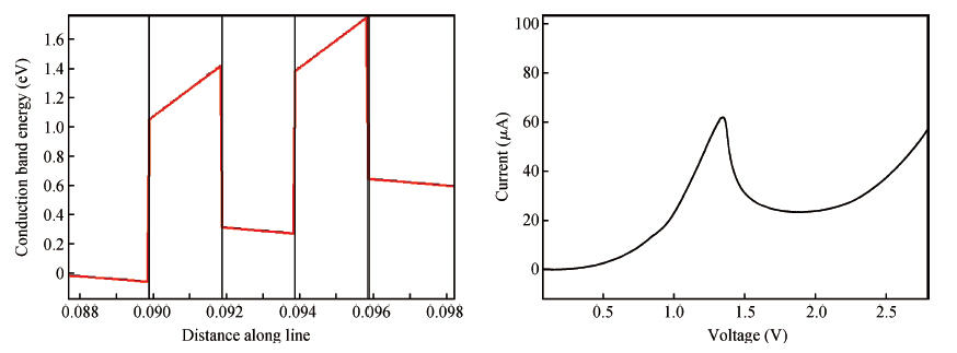
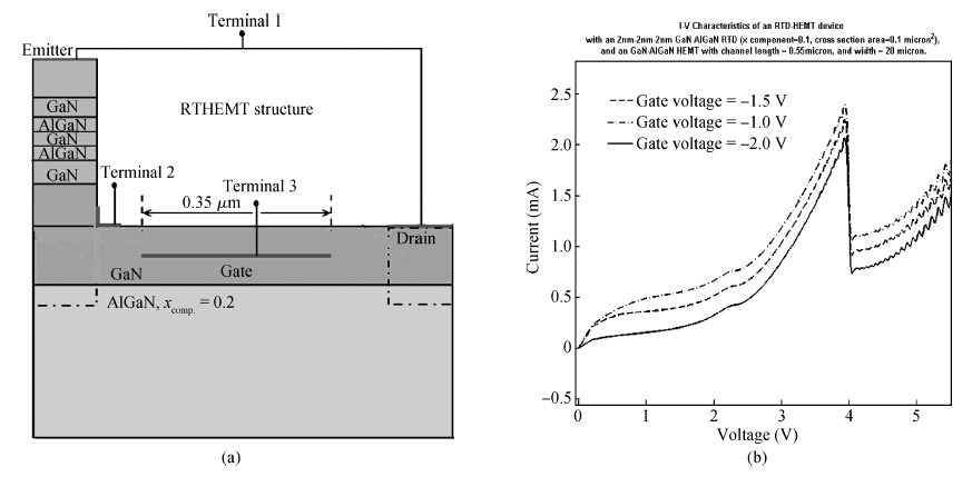
For the first time, we have introduced a novel GaN based resonant tunneling high electron mobility transistor (RTHEMT) on a silicon substrate. A monolithically integrated GaN based inverted high electron mobility transistor (HEMT) and a resonant tunneling diode (RTD) are designed and simulated using the ATLAS simulator and MATLAB in this study. The 10% Al composition in the barrier layer of the GaN based RTD structure provides a peak-to-valley current ratio of 2.66 which controls the GaN based HEMT performance. Thus the results indicate an improvement in the current-voltage characteristics of the RTHEMT by controlling the gate voltage in this structure. The introduction of silicon as a substrate is a unique step taken by us for this type of RTHEMT structure.

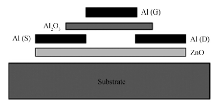
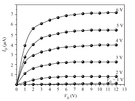
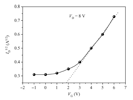
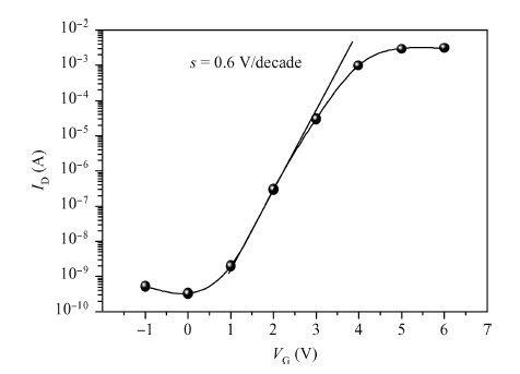
ZnO thin films were prepared by a simple chemical bath deposition technique using an inorganic solution mixture of ZnCl2 and NH3 on glass substrates and then were used as the active material in thin film transistors (TFTs). The TFTs were fabricated in a top gate coplanar electrode structure with high-k Al2O3 as the gate insulator and Al as the source, drain and gate electrodes. The TFTs were annealed in air at 500 ℃ for 1 h. The TFTs with a 50 μm channel length exhibited a high field-effect mobility of 0.45 cm2/(V·s) and a low threshold voltage of 1.8 V. The sub-threshold swing and drain current ON-OFF ratio were found to be 0.6 V/dec and 106, respectively.

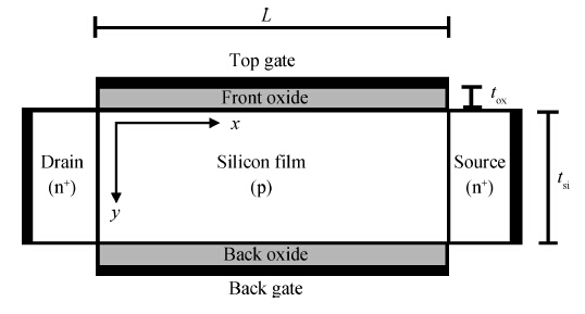
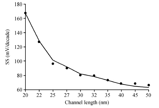
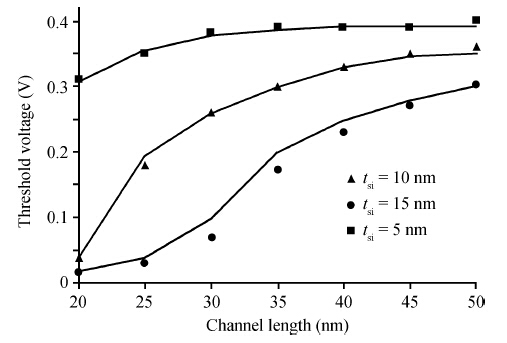
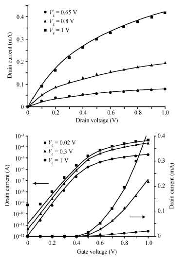
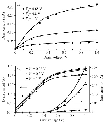
A 2D model for the potential distribution in silicon film is derived for a symmetrical double gate MOSFET in weak inversion. This 2D potential distribution model is used to analytically derive an expression for the subthreshold slope and threshold voltage. A drain current model for lightly doped symmetrical DG MOSFETs is then presented by considering weak and strong inversion regions including short channel effects, series source to drain resistance and channel length modulation parameters. These derived models are compared with the simulation results of the SILVACO (Atlas) tool for different channel lengths and silicon film thicknesses. Lastly, the effect of the fixed oxide charge on the drain current model has been studied through simulation. It is observed that the obtained analytical models of symmetrical double gate MOSFETs are in good agreement with the simulated results for a channel length to silicon film thickness ratio greater than or equal to 2.
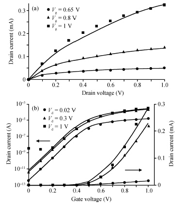
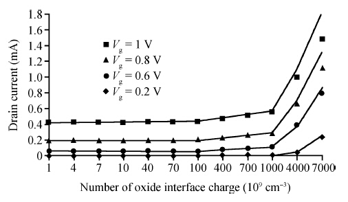

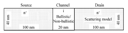
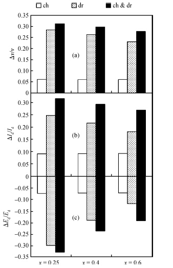
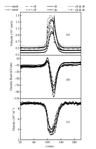
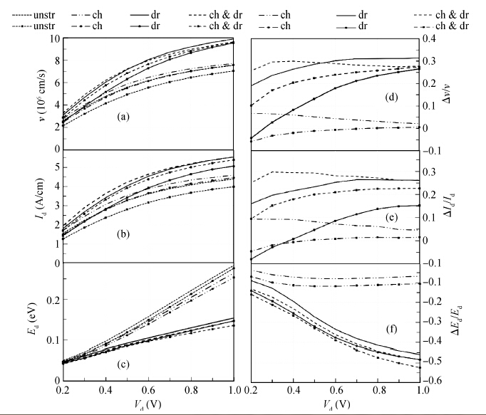
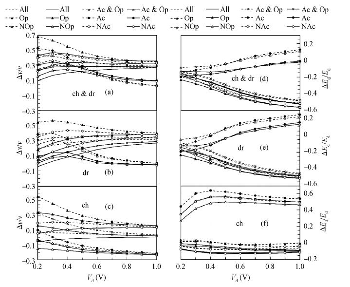
The effects of multiple scattering on the electron transport properties in drain regions are numerically investigated for the cases of strained-Si diodes with or without scattering in the channel. The performance of non-ballistic (with scattering) channel Si-diodes is compared with that of ballistic (without scattering) channel Si-diodes, using the strain and scattering model. Our results show that the values of the electron velocity and the current in the strain model are higher than the respective values in the unstrained model, and the values of the velocity and the current in the ballistic channel model are higher than the respective values in the non-ballistic channel model. In the strain and scattering models, the effect of each carrier scattering mechanism on the performance of the Si-diodes is analyzed in the drain region. For the ballistic channel model, our results show that inter-valley optical phonon scattering improves device performance, whereas intra-valley acoustic phonon scattering degrades device performance. For the strain model, our results imply that the larger energy splitting of the strained Si could suppress the inter-valley phonon scattering rate. In conclusion, for the drain region, investigation of the strained-Si and scattering mechanisms are necessary, in order to improve the performance of nanoscale ballistic regime devices.

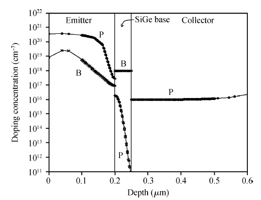
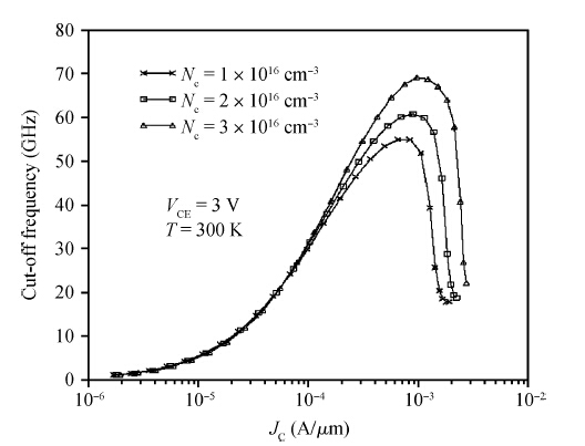
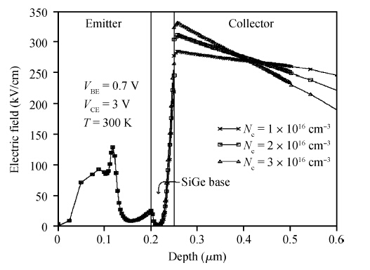
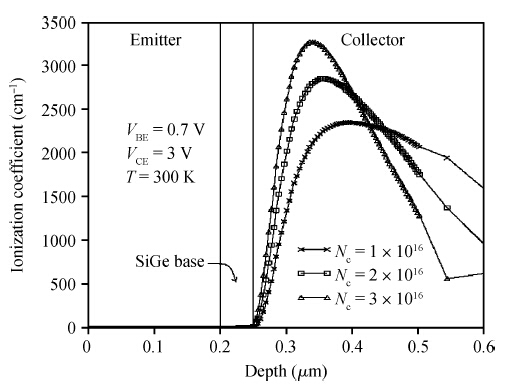
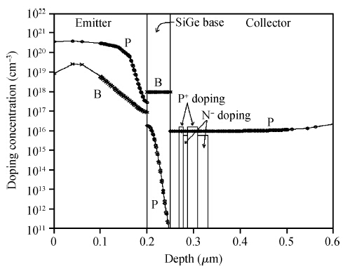
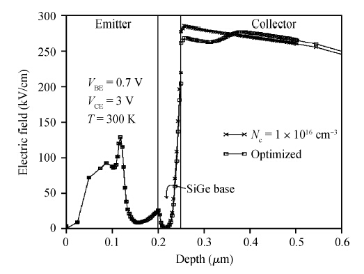
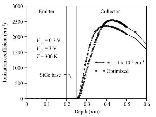
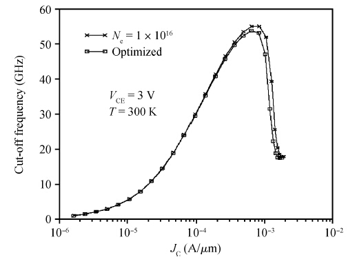
BVCESfT rather than BVCEOfT is employed in representing the limit of the product of the breakdown voltage-cutoff frequency in SiGe HBT for collector engineering design. Instead of a single decrease in collector doping to improve BVCESfT and BVCEOfT, a novel optimization collector doping design is presented to improve the well-known tradeoff between the breakdown voltage and cut-off frequency in SiGe HBT. As a result, the BVCESfT product is improved from 537.57 to 556.4 GHz·V, and the BVCEOfT product is improved from 309.51 to 326.35 GHz·V.

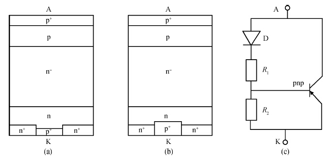
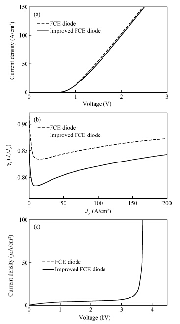
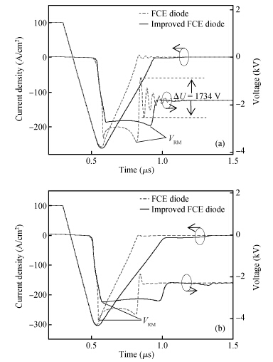
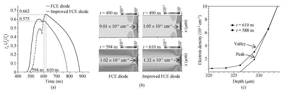
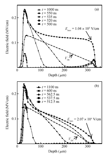
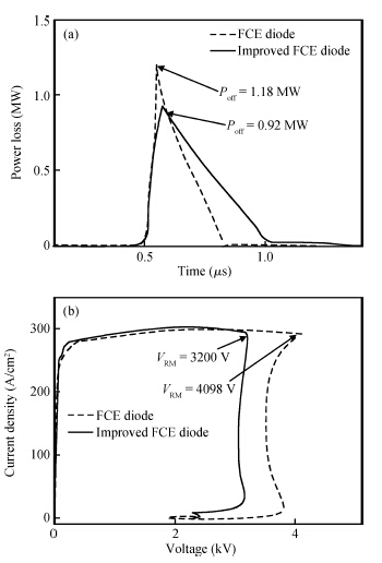
An improved field charge extraction (FCE) diode with a deep p+ adjusting region at the cathode side is studied. The reverse recovery mechanism and electric field gradient are thoroughly analyzed and validated using ISE simulation results. The results show that, based on the premise of ensuring the static characteristics, the improved FCE diode can clearly improve the softness and effectively suppress the peak electric field of the nn- junction at the cathode side during reverse recovery, and thus has a high dynamic avalanche capability compared with conventional FCE diodes.

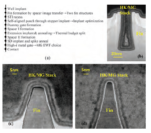
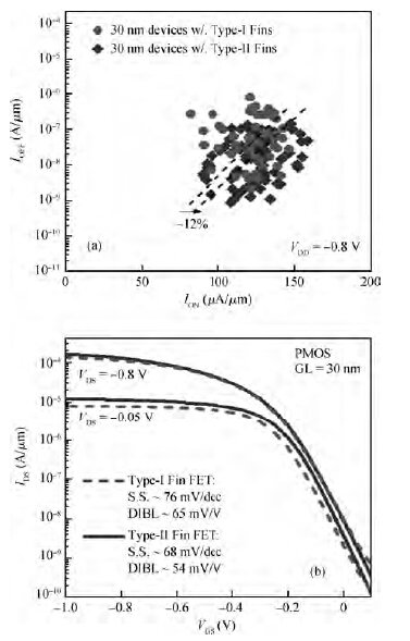
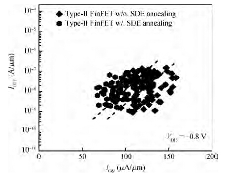
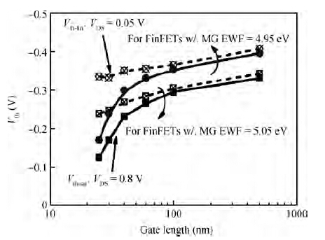
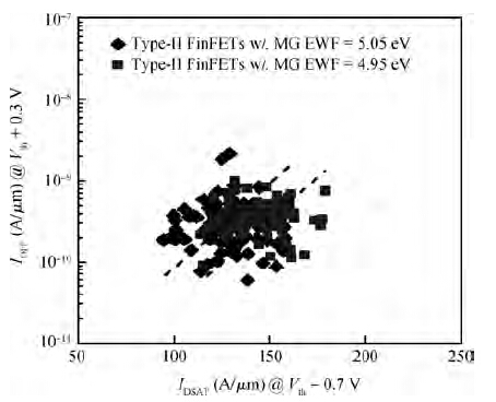
Sub-20 nm node bulk FinFET PMOS devices with an all-last high-k/metal gate (HK/MG) process are fabricated and the influence of a series of device parameters on the device scaling is investigated. The high and thin Fin structure with a tapered sidewall shows better performance than the normal Fin structure. The punch through stop layer (PTSL) and source drain extension (SDE) doping profiles are carefully optimized. The device without SDE annealing shows a larger drive current than that with SDE annealing due to better Si crystal regrowth in the amorphous Fin structure after source/drain implantation. The band-edged MG has a better short channel effect immunity, but the lower effective work function (EWF) MG shows a larger driveability. A tradeoff choice for different EWF MGs should be carefully designed for the device's scaling.

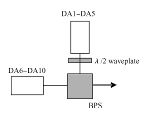
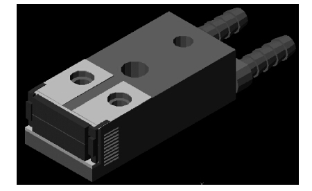
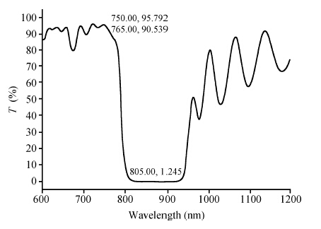
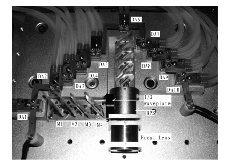
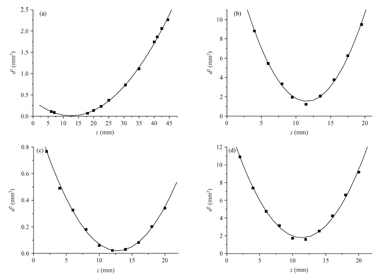
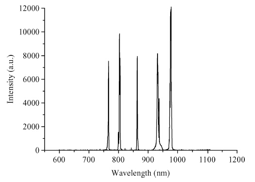
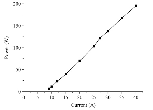
Design and experimental studies on the wavelength multiplexing and polarization multiplexing of diode laser arrays were carried out. First, the structure of a AlGaInAs/GaAs/AlGaAs quantum well under compressive strain was used because the characteristic of wavelength was easier to adjust. We obtained diode laser arrays lasing in five different wavelengths, about 760 nm, 800 nm, 860 nm, 930 nm, and 976 nm. At the same time, four edge filters were designed, and an experimental study on the beam multiplexing of diode laser arrays was carried out. Second, two beams with different polarization states were composited using a half wave plate and a polarizing beam-splitter prism. After that, the beam focusing system was designed. Ultimately, ten beams of diode laser arrays in five wavelengths and two polarization states were composited, the total output power was 196 W and the overall efficiency was 76%. The size of the output focus spot was 144 × 1330 μm2, and the power density of the focused light was as high as 1.02 × 10⁵ W/cm2. Compared with a single diode laser array, the power density of the composite beam was improved by 4.3 times.

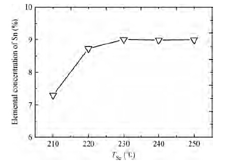
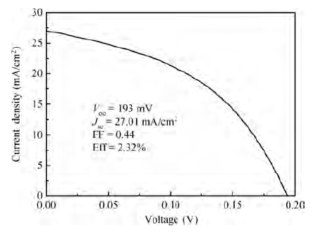
Cu2ZnSnSe4 (CZTSe) thin film solar cells have been fabricated using a one-step co-evaporation technique. The structural properties of polycrystalline CZTSe films deposited at different selenium evaporation temperatures (TSe) have been investigated using X-ray diffraction spectra, scanning electron microscopy, and atomic force microscopy. A relationship between TSe and the secondary phases deposited in the initial stage is established to explain the experimental observations. The Se flux is not necessarily increased too much to reduce Sn loss and the consumption of Se during fabrication could also be reduced. The best solar cell, with an efficiency of 2.32%, was obtained at a medium TSe of 230 ℃ (active area 0.34 cm2).

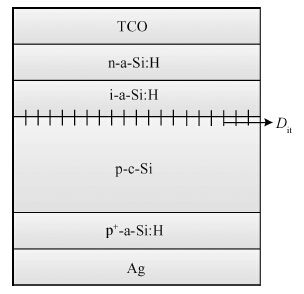
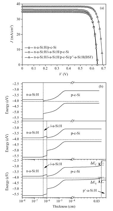
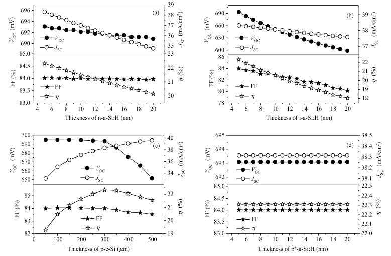
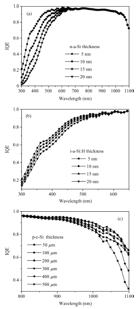
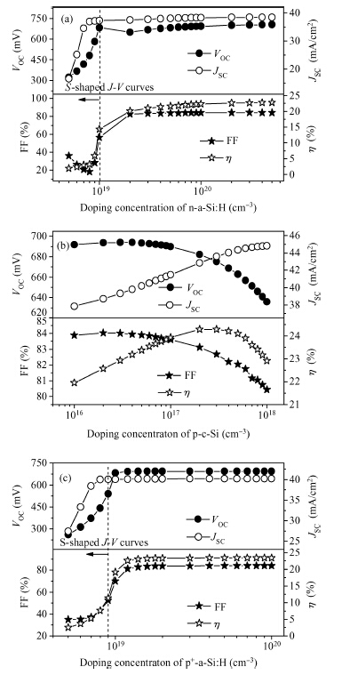
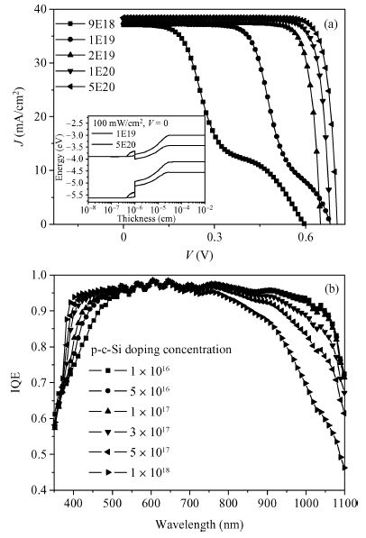
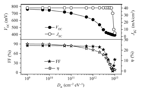
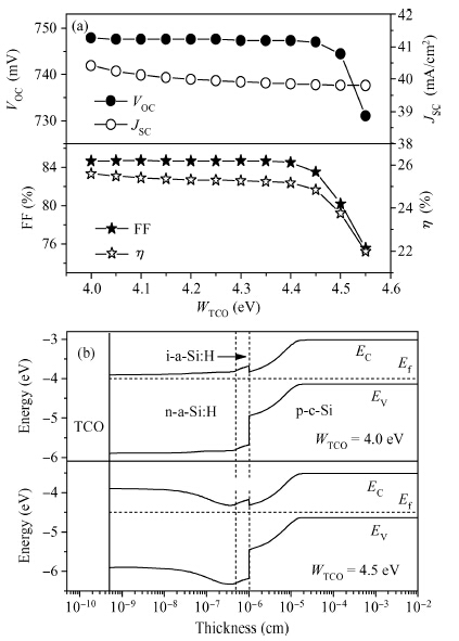
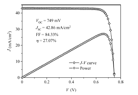
The basic parameters of a-Si:H/c-Si heterojunction solar cells, such as layer thickness, doping concentration, a-Si:H/c-Si interface defect density, and the work functions of the transparent conducting oxide (TCO) and back surface field (BSF) layer, are crucial factors that influence the carrier transport properties and the efficiency of the solar cells. The correlations between the carrier transport properties and these parameters and the performance of a-Si:H/c-Si heterojunction solar cells were investigated using the AFORS-HET program. Through the analysis and optimization of a TCO/n-a-Si:H/i-a-Si:H/p-c-Si/p+-a-Si:H/Ag solar cell, a photoelectric conversion efficiency of 27.07% (VOC: 749 mV, JSC: 42.86 mA/cm2, FF: 84.33%) was obtained through simulation. An in-depth understanding of the transport properties can help to improve the efficiency of a-Si:H/c-Si heterojunction solar cells, and provide useful guidance for actual heterojunction with intrinsic thin layer (HIT) solar cell manufacturing.

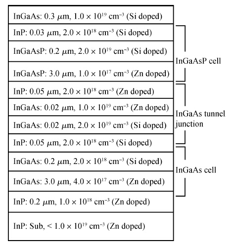
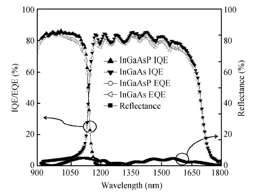
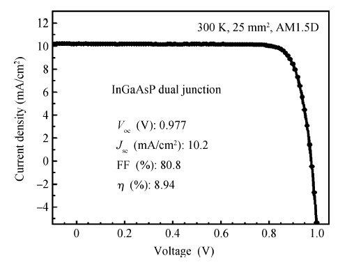
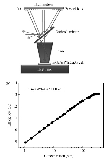
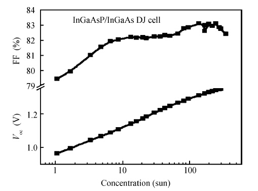
Lattice-matched InGaAs(P) photovoltaic devices were grown on InP substrates by metal-organic chemical vapor deposition. InGaAsP/InGaAs (1.07/0.74 eV) dual-junction (DJ) solar cells were fabricated and characterized by quantum efficiency and I-V measurements. The open circuit voltage, short circuit current density, fill factor, and efficiency of InGaAsP/InGaAs DJ solar cell are 0.977 V, 10.2 mA/cm2, 80.8%, and 8.94%, respectively, under one sun illumination of the AM 1.5D spectrum. For the InGaAsP/InGaAs DJ solar cell, with increasing concentration, the conversion efficiency first increases steadily and reaches 13% around 280 suns, and finally decreases due to the drop in fill factor at higher concentration ratios. These experimental results demonstrate the promising prospect of GaInP/GaAs/InGaAsP/InGaAs four-junction solar cells.

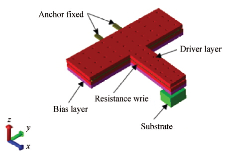
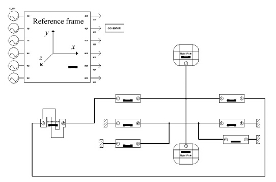
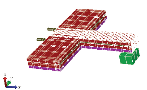
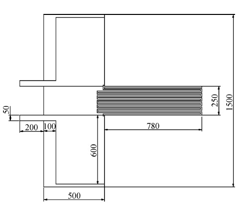
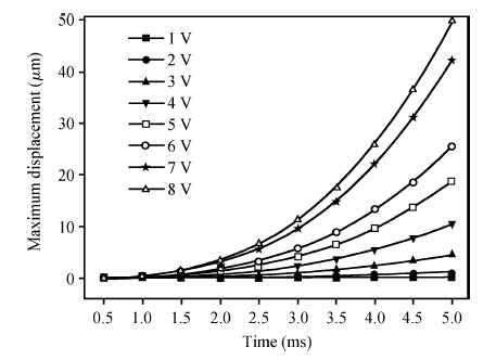
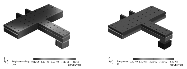
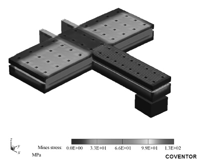
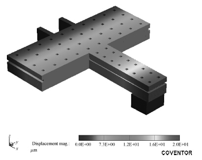
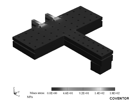
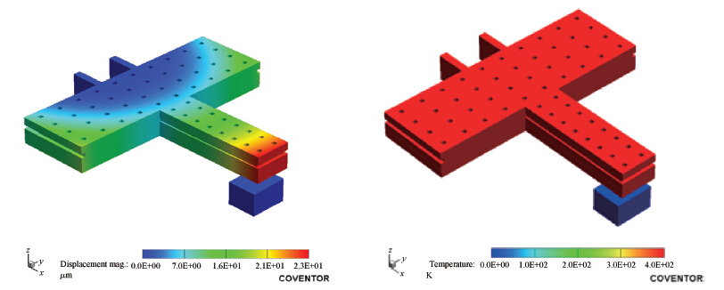
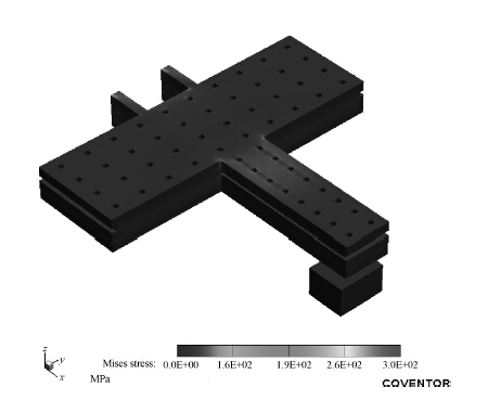
This paper introduces a type of out-of-plane microelectrothermal actuator, which is based on the principle of bimetal film thermal expansion in the fuse. A polymer SU-8 material and nickel are used as the functional and structural materials of the actuator. Through heating the resistance wire using electricity, the actuator produces out-of-plane motion in the perpendicular axial direction of the device and the bias layer contact with the substrate, completing signal output. Using Coventorware software to establish the three-dimensional model, the geometric structure is optimized and the electrothermal capabilities are determined theoretically. From electrothermal analysis, the actuator's displacement is 18 μm and the temperature rises from 300 to 440 K under a voltage of 5 V and the response time is 5 ms. The actuator's displacement is 20 μm under a 100000 m/s2 acceleration in the accelerating field. In the coupled field, applying a 3 V voltage, the initial temperature is 300 K, while the acceleration is 50000 m/s2, the driving displacement of the actuator is 23 μm, and temperature rises to 400 K. Finally, through checking the stress in different field sources, the maximum stress of the actuator is smaller than the allowable stress of nickel. The results show that the electrothermal actuator has high reliability.

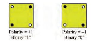
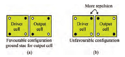
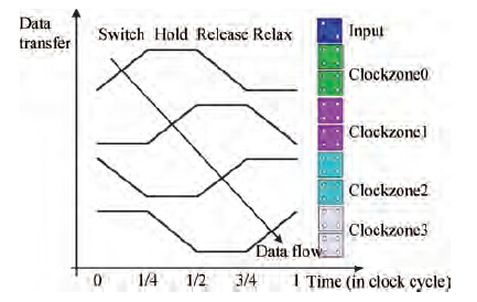
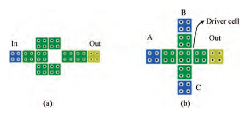
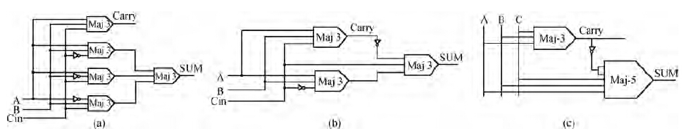
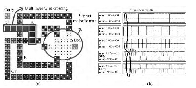
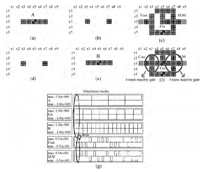
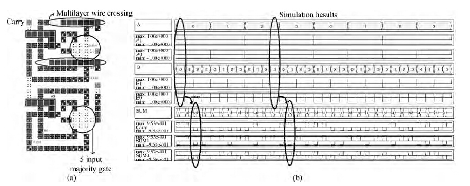
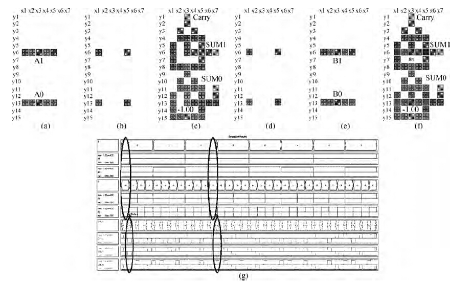
This paper proposes a novel design paradigm for circuits designed in quantum dot cellular automata (QCA) technology. Previously reported QCA circuits in the literature have generally been designed in a single layer which is the main logical block in which the inverter and majority gate are on the base layer, except for the parts where multilayer wire crossing was used. In this paper the concept of multilayer wire crossing has been extended to design logic gates in multilayers. Using a 5-input majority gate in a multilayer, a 1-bit and 2-bit adder have been designed in the proposed multilayer gate design paradigm. A comparison has been made with some adders reported previously in the literature and it has been shown that circuits designed in the proposed design paradigm are much more efficient in terms of area, the requirement of QCA cells in the design and the input-output delay of the circuit. Over all, the availability of one additional spatial dimension makes the design process much more flexible and there is scope for the customizability of logic gate designs to make the circuit compact.

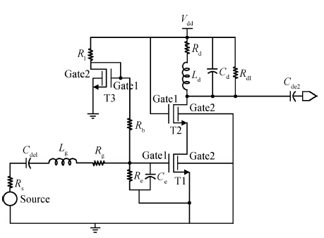
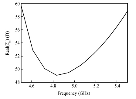
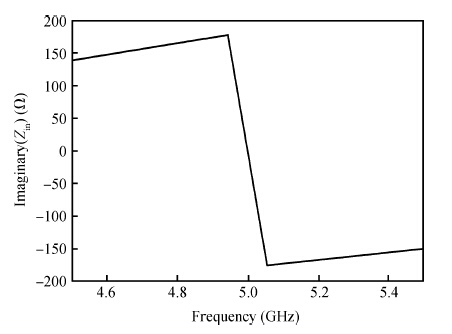
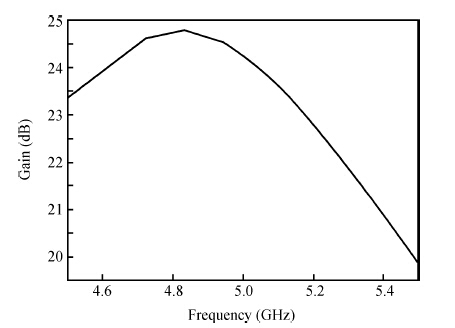
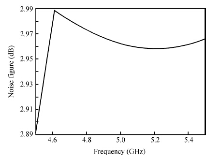
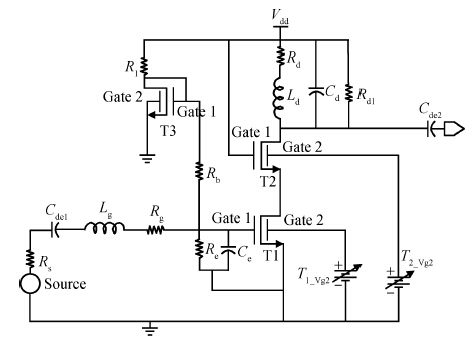
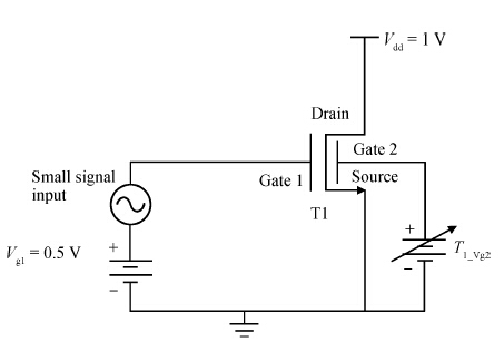
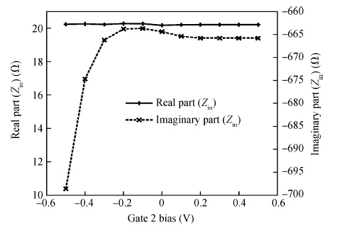
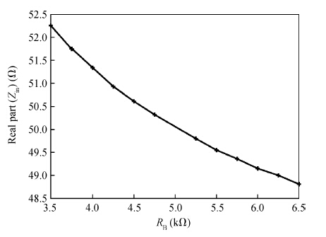
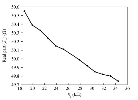
The effect of process variations of a FinFET-based low noise amplifier (LNA) are mitigated by using the device in an independently driven mode, i.e. an independently driven double gate (IDDG) FinFET. A 45 nm gate length IDDG FinFET-based cascoded LNA, operating at 5 GHz, is designed and studied to assess the impact of process variation on the LNA performance metrics such as input impedance, gain and noise figure. Four geometrical parameters, gate length, channel width, gate oxide thickness and fin width, and one non-geometrical parameter, channel doping concentration, are considered in the study. The effect of these variations on the input impedance (the desired value is 50 Ω purely real) of the LNA is compensated by the second gate bias of the IDDG FinFET.

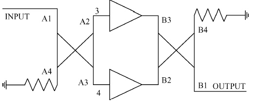
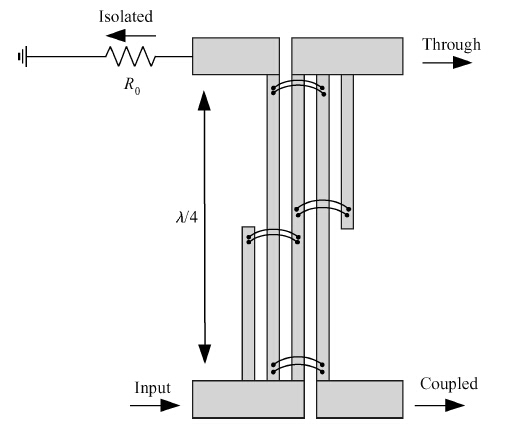
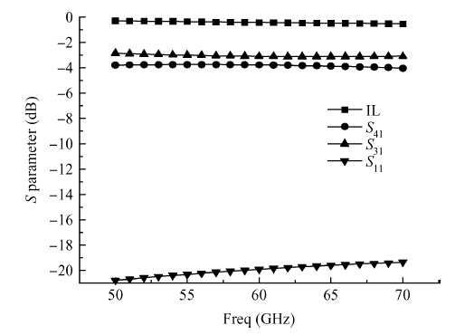
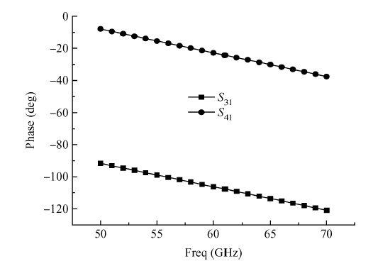
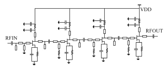
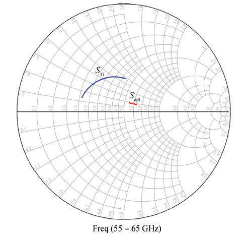
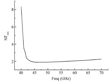
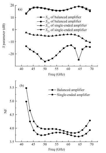
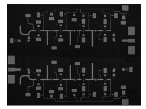
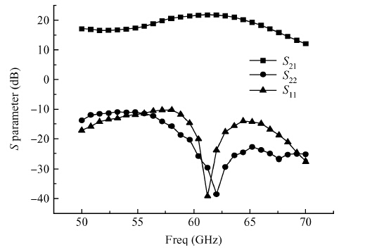
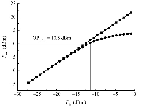
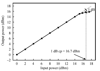
This paper presents a 60 GHz balanced low noise amplifier. Compared with single-ended structures, the balanced structure can obtain a better input/output return loss, a lower noise figure (NF), a 3 dB improvement of the 1 dB compression point, a 6 dB improvement of IM3 and a doubled dynamic range. Each single-ended amplifier in this paper uses a four-stage cascade structure to achieve a high gain in broadband. At the operating frequency range of 59-64 GHz, the small signal gain of the balanced amplifier is more than 20 dB. Both the input and output return losses are less than -12 dB. The output 1 dB compression power is 10.5 dBm at 60 GHz. The simulation result for the NF is better than 3.9 dB. The chip is fabricated using a 0.15 μm GaAs pHEMT process with a size of 2.25 × 1.7 mm2.

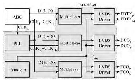
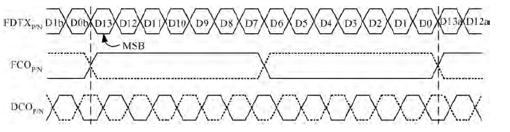
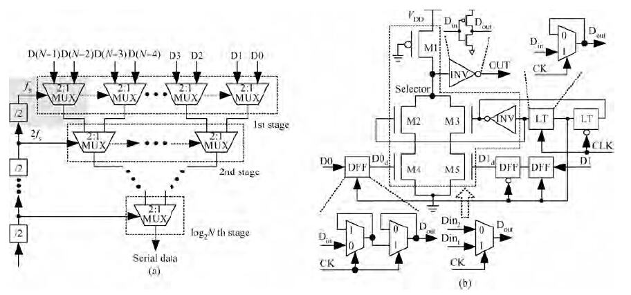
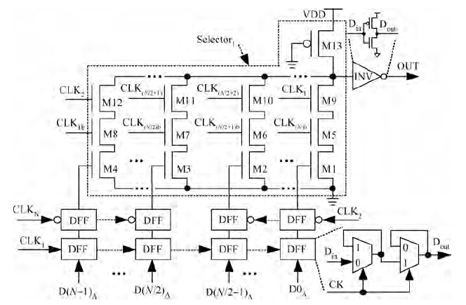
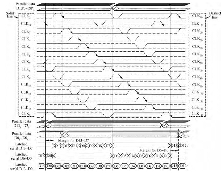
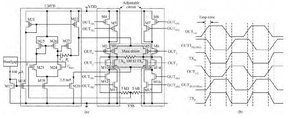
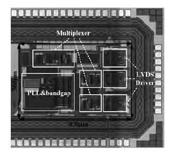
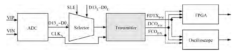
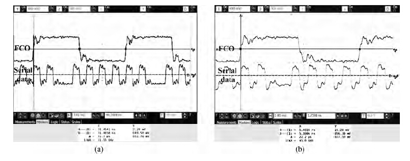
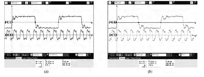
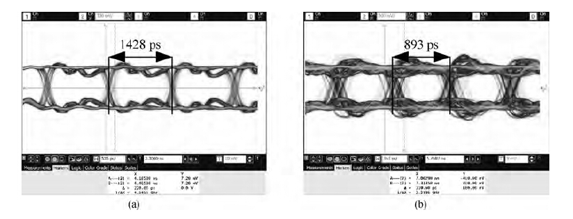
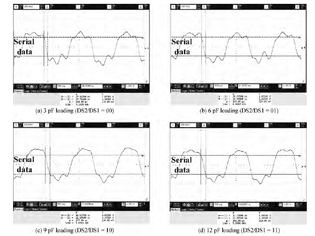
This paper presents a 1.12 Gb/s 11.3 mW transmitter using 0.18 μm mixed signal complementary metal-oxide semiconductor technology with a 1.8 V supply voltage. This transmitter implements a high-speed transmission with 1.2 V common-mode output voltage, adopting a low-voltage differential signaling (LVDS) technique. A multiplexer (MUX) and an LVDS driver are critical for a transmitter to complete a high-speed data transmission. This paper proposes a high power-efficiency single-stage 14 : 1 MUX and an adjustable LVDS driver circuit, capable of driving different loads with a slight increase in power consumption. The prototype chip implements a transmitter with a core area of 970 × 560 μm2, demonstrating low power consumption and adjustable driving capability.

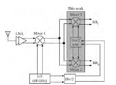
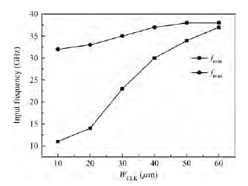
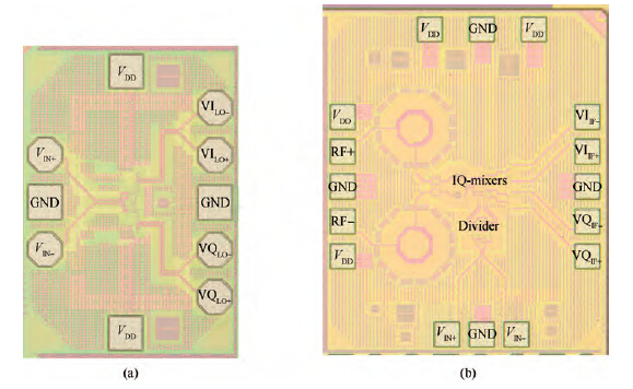
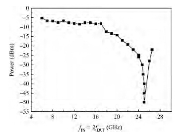
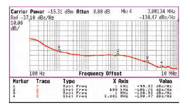
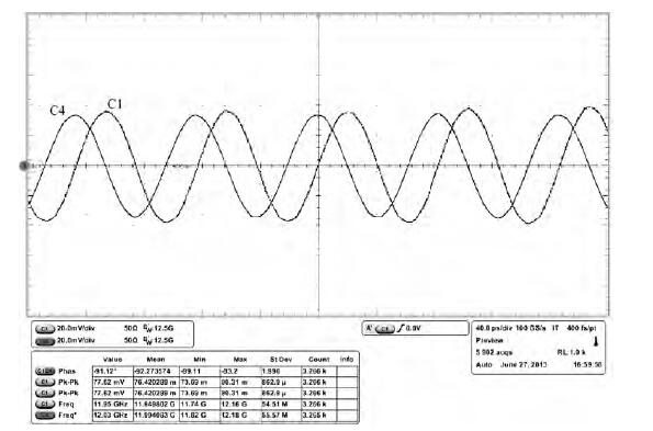
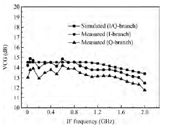
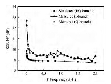
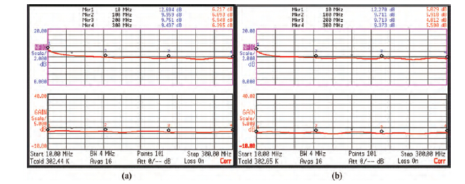
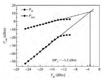
This paper presents the design of a low power (LP) and a low noise figure (NF) quadrature demodulator with an on-chip frequency divider for quadrature local oscillator (LO) signal generation. The transconductance stage of the mixer is implemented by an AC-coupled self-bias current reuse topology. On-chip series inductors are employed at the gate terminals of the differential input transconductance stage to improve the voltage gain by enhancing the effective transconductance. The chip is implemented in 65-nm LP CMOS technology. The demodulator is designed for an input radio frequency (RF) band ranging from 10.25 to 13.75 GHz. A fixed LO frequency of 12 GHz down-converts the RF band to an intermediate frequency (IF) band ranging from DC to 1.75 GHz. From 10 MHz to 1.75 GHz the demodulator achieves a voltage conversion gain (VCG) ranging from 14.2 to 13.2 dB, and a minimum single-sideband NF (SSB-NF) of 9 dB. The measured third-order input intercept point (IIP3) is -3.3 dBm for a two-tone test frequency spacing of 1 MHz. The mixer alone draws a current of only 2.5 mA, whereas the complete demodulator draws a current of 7.18 mA from a 1.2 V supply. The measurement results for a frequency divider, which was fabricated individually, prior to being integrated with the quadrature demodulator, in 65-nm LP CMOS technology, are also presented in this paper.
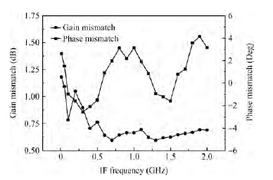

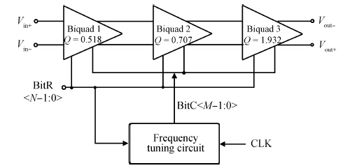
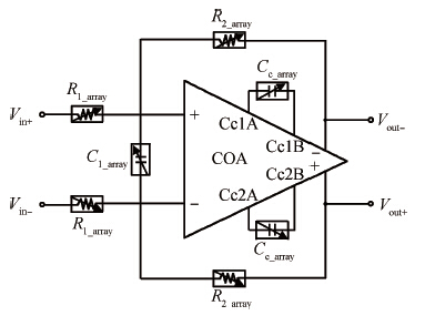
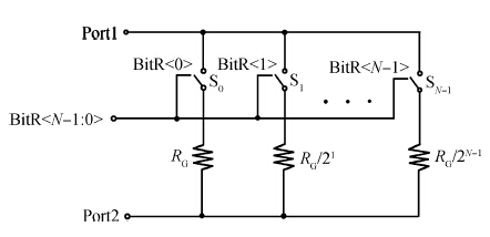
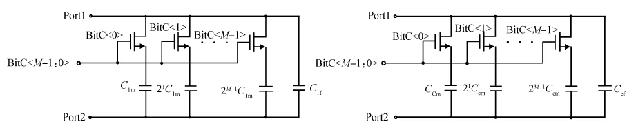
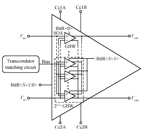
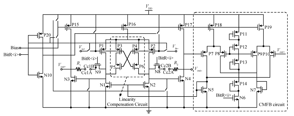
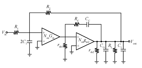
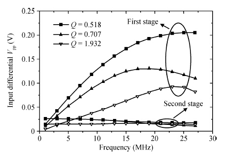
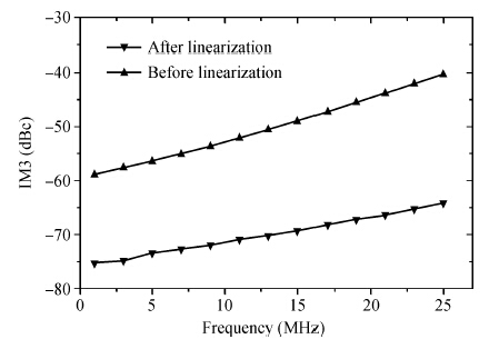
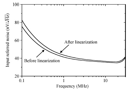
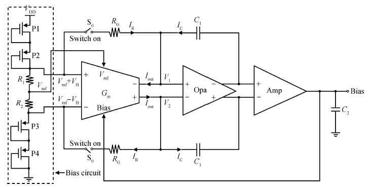
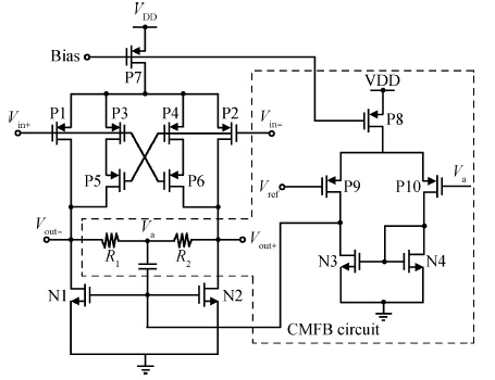
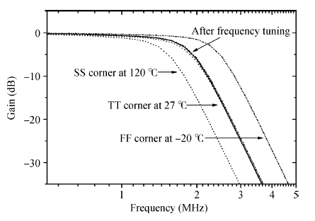
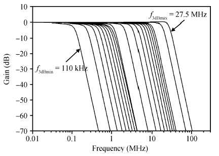
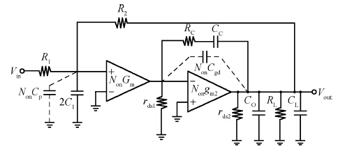
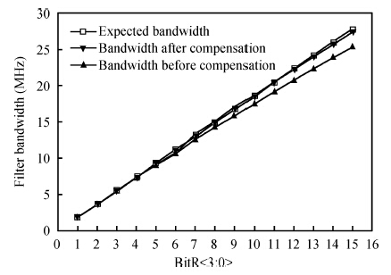
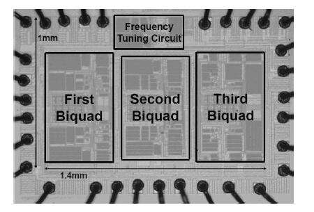
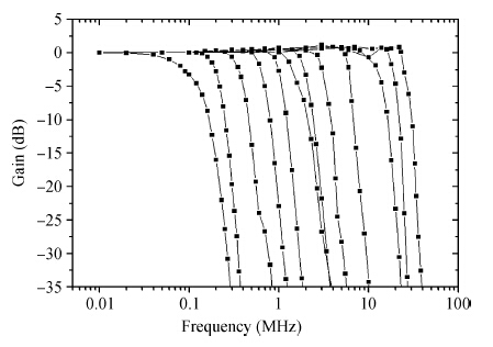
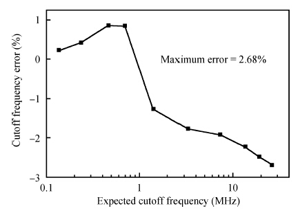
This paper presents the design and implementation of a low power wide tuning range baseband filter with an accurate on-chip tuning circuit for reconfigurable multistandard wireless transceivers. The realized low pass filter (LPF) is a six-order Butterworth type by cascading three stage active-Gm-RC biquadratic cells. A modified linearization technique is used to improve the filter linearity performance at low power consumption. A new process-independent transconductor matching circuit and a new frequency tuning circuit with frequency compensation are proposed to achieve a high precision filter frequency response. The proposed LPF is realized in a 130 nm standard CMOS technology. The measured results show that the LPF exhibits a high bandwidth programmability from 0.1 to 25 MHz with a tuning frequency error less than 2.68% over the wide tuning range. The power consumption is scalable, ranging from 0.52 to 5.25 mA, from a 1.2 V power supply while achieving a 26.3 dBm in-band IIP3.

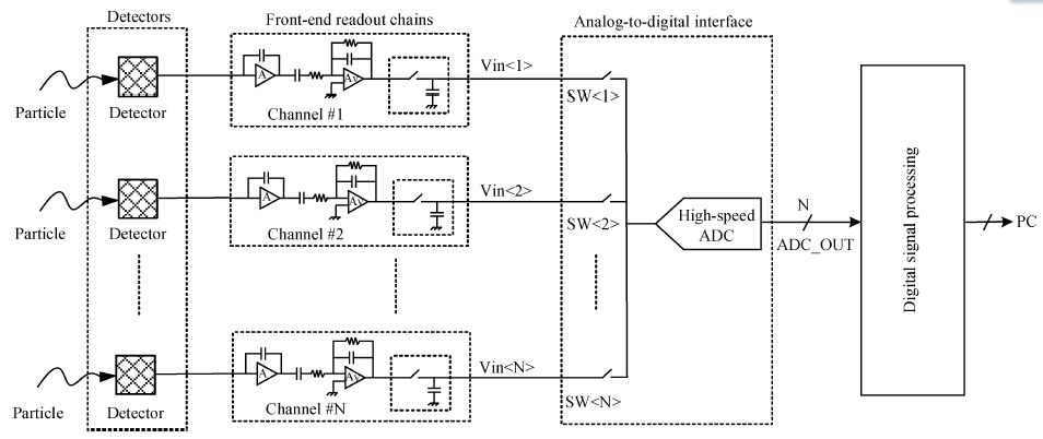
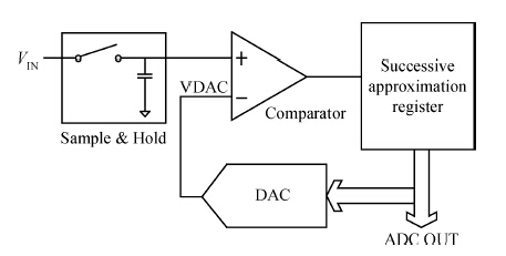
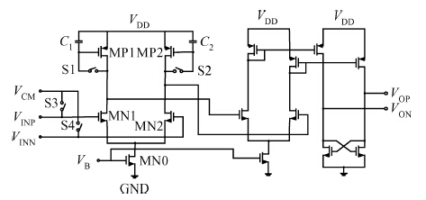
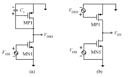
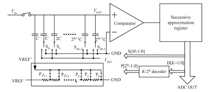
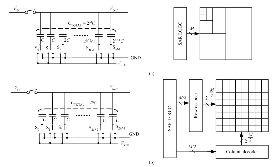
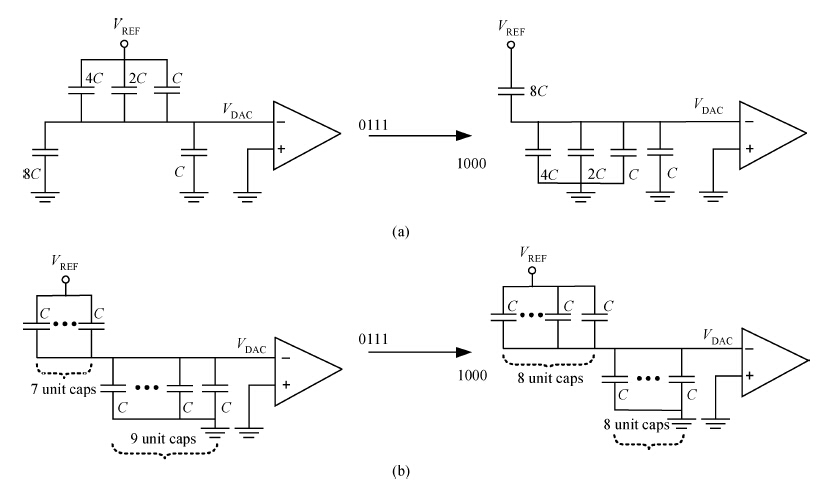
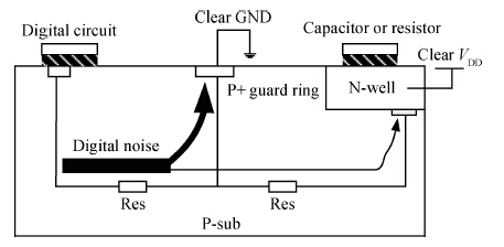
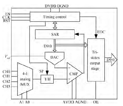
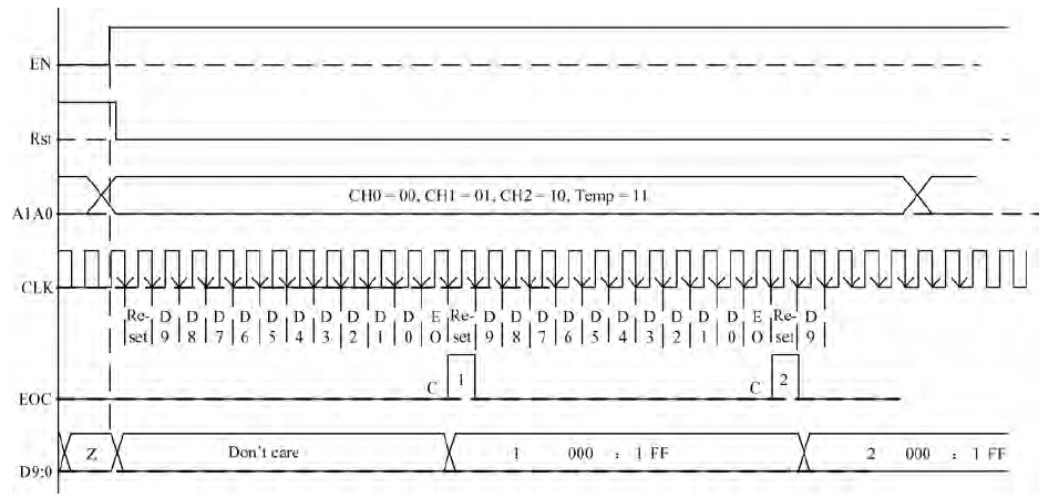
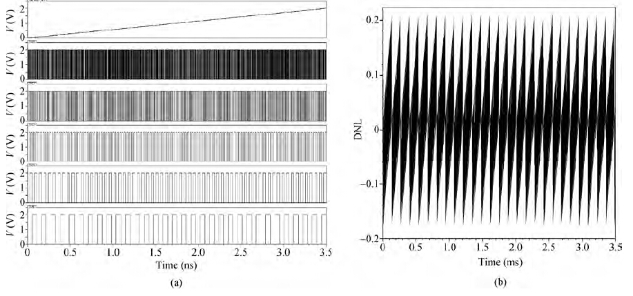
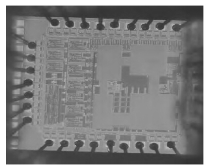
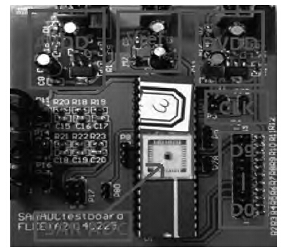
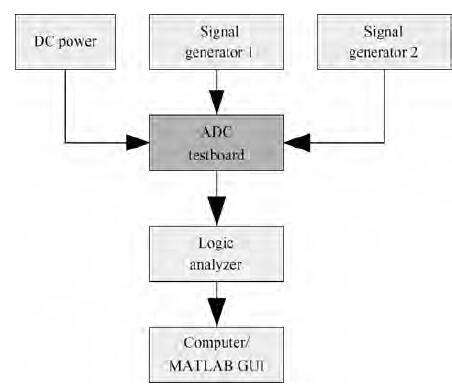
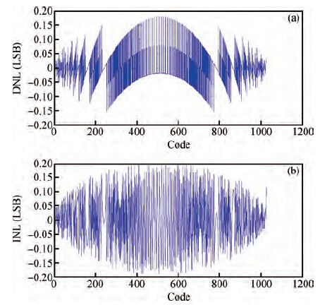
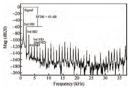
This paper presents a low power, area-efficient and radiation-hardened 12-bit 1 MS/s successive approximation register (SAR) analog-to-digital converter (ADC) for multi-channel CdZnTe (CZT) detector applications. In order to improve the SAR-ADC's accuracy, a novel comparator is proposed in which the offset voltage is self-calibrated and also a new architecture for the unit capacitor array is proposed to reduce the capacitance mismatches in the charge-redistribution DAC. The ability to radiation-harden the SAR-ADC is enhanced through circuit and layout design technologies. The prototype chip was fabricated using a TSMC 0.35 μm 2P4M CMOS process. At a 3.3/5 V power supply and a sampling rate of 1 MS/s, the proposed SAR-ADC achieves a peak signal to noise and distortion ratio (SINAD) of 67.64 dB and consumes only 10 mW power. The core of the prototype chip occupies an active area of 1180 × 1080 μm2.

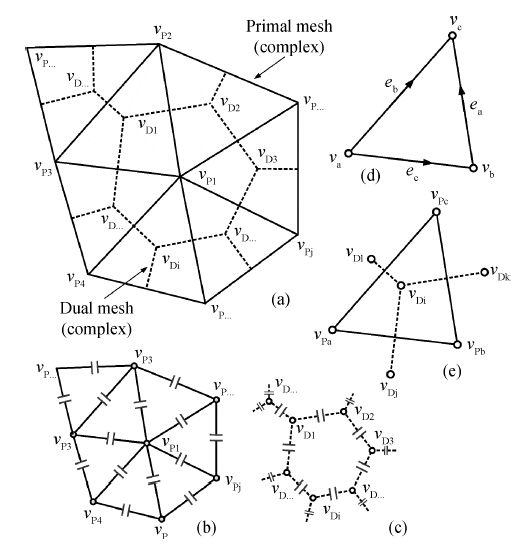
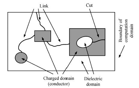
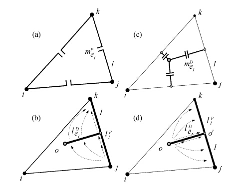
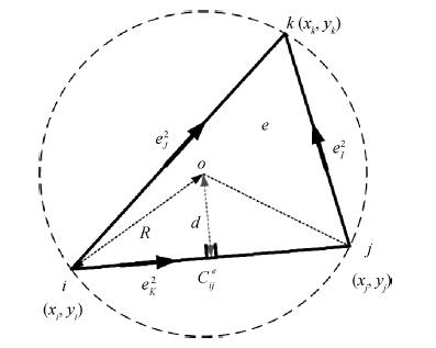
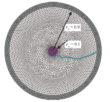
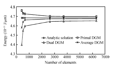
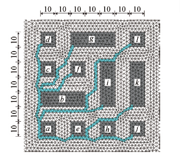
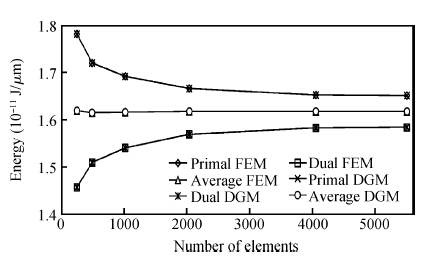
Capacitance extraction is one of the key issues in integrated circuits and also a typical electrostatic problem. The dual discrete geometric method (DGM) is investigated to provide relative solutions in two-dimensional unstructured mesh space. The energy complementary characteristic and quick field energy computation thereof based on it are emphasized. Contrastive analysis between the dual finite element methods and the dual DGMs are presented both from theoretical derivation and through case studies. The DGM, taking the scalar potential as unknown on dual interlocked meshes, with simple form and good accuracy, is expected to be one of the mainstreaming methods in associated areas.

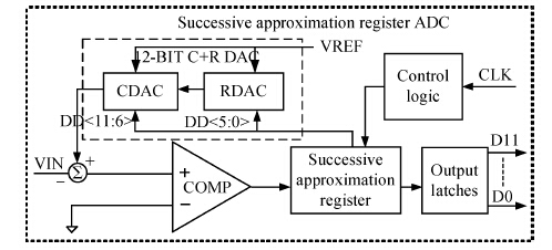
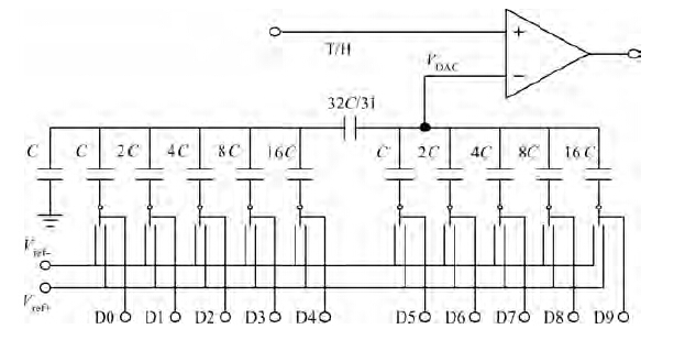
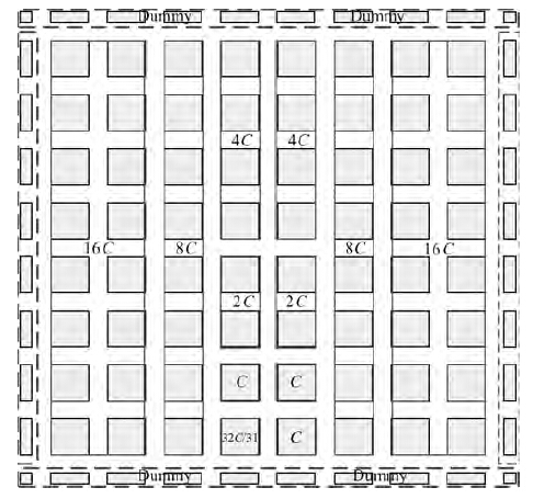
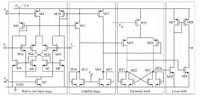
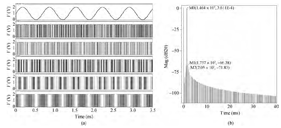
This paper presents a low power 10 bit 300 ksps successive approximation register analog-to-digital converter (SAR ADC) which is applied in wireless sensor network (WSN) applications. A single ended energy-saving split capacitor DAC array and a latch comparator with a rail to rail input stage are utilized to implement the ADC, which can reduce power dissipation while expanding the full scale input range and improve the signal-to-noise ratio (SNR). For power optimization the supply voltage of the SAR ADC is designed to be as low as 2 V. Four analog input channels are designed which make the ADC more suitable for WSN applications. The prototype circuit is fabricated using 3.3 V, 0.35 μm 2P4M CMOS technology and occupies an active chip area of 1.23 mm2. The test results show that the power dissipation is only 200 μW at a 2 V power supply and a sampling rate of 166 kSps. The calculated SNR is 58.25 dB, the ENOB is 9.38 bit and the FOM is 4.95 pJ/conversion-step.

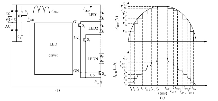
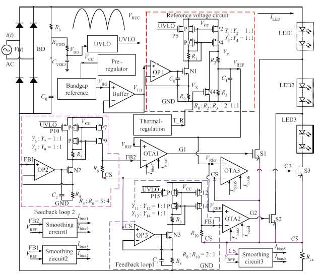
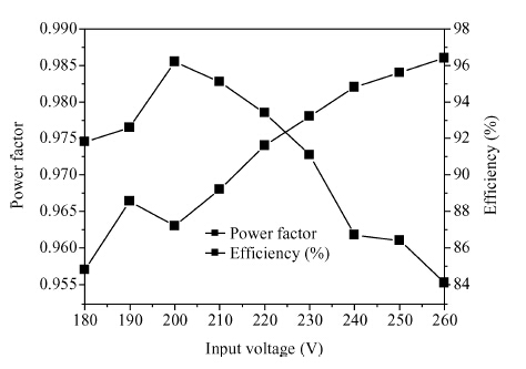
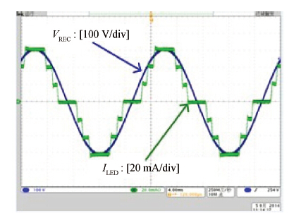
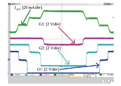
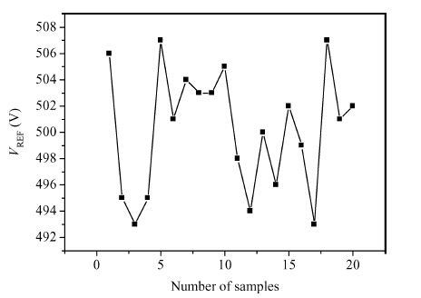
A high efficiency, high power factor, and linear constant current LED driver based on adaptive segmented linear architecture is presented. When the input voltage varied, the proposed LED driver automatically switched over LED strings according to the segmented LED voltage drop, which increased the LED lighting time. The efficiency and power-factor are improved, while the system design is simplified by this control scheme. Without the usage of electrolytic capacitor and magnetic components, the proposed driver possesses advantages of smaller size, longer lifetime and lower cost over others. The proposed driver is implemented in 0.8 μm 5 V/40 V HVCMOS process, which occupies an active area of 820 × 920 μm2. The measured results show that the average value of the internal reference voltage is 500 ± 7 mV, with a standard deviation of only 4.629 mV, thus LED current can be set accurately. Under 220 V root mean square 50 Hz utility voltage and the number ratio of the three LED strings being 47 : 17 : 16, the system can realize a high power factor of 0.974 and power conversion efficiency of 93.4%.

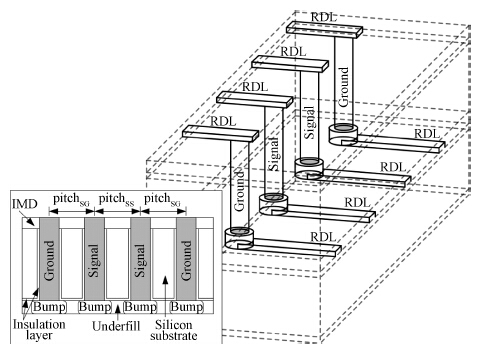
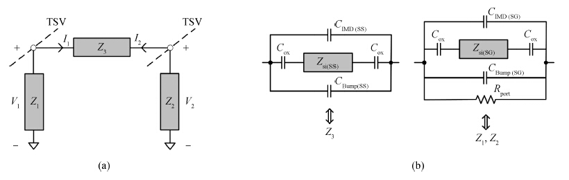
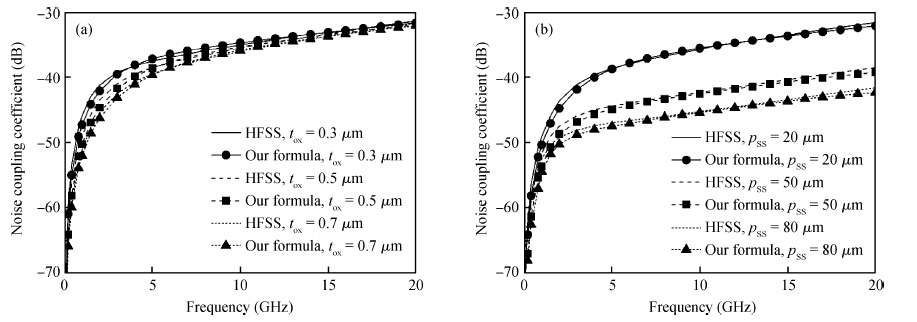
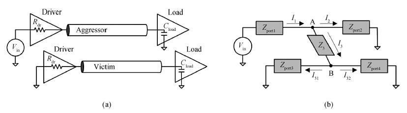
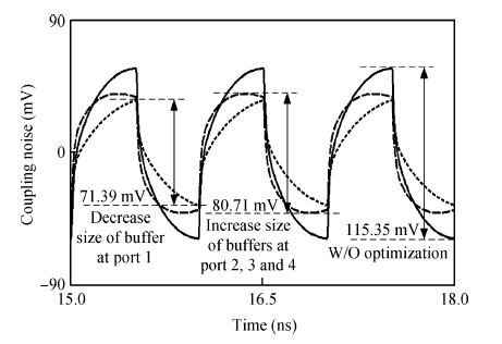
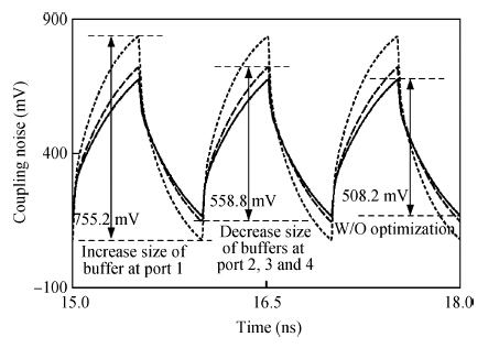
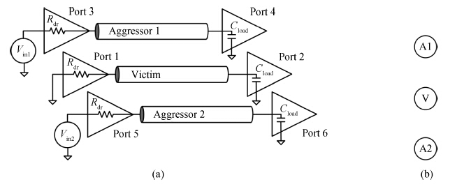
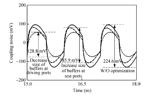
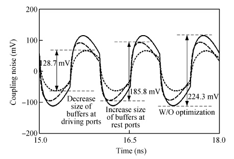
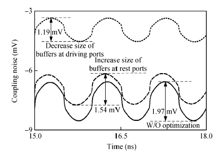
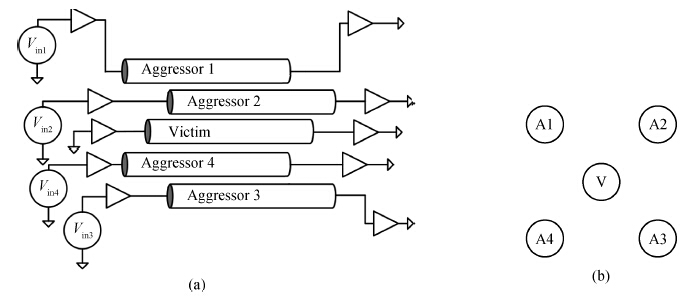
Through silicon via (TSV)-TSV coupling is detrimental to the performance of three-dimensional (3D) integrated circuits (ICs) with the major negative effect of introducing coupling noise. In order to obtain an accurate estimation of the coupling level from TSV-TSV in the early design stage, this paper first proposes an impedance-level model of the coupling channel between TSVs based on a two-port network, and then derives the formula of the coupling coefficient to describe the TSV-TSV coupling effect. The accuracy of the formula is validated by comparing the results with 3D full-wave simulations. Furthermore, a design technique for optimizing the coupling between adjacent coupled signal TSVs is proposed. Through SPICE simulations, the proposed technique shows its feasibility to reduce the coupling noise for both a simple TSV-TSV circuit and a complicated circuit with more TSVs, and demonstrates its potential for designers in achieving the goal of improving the electrical performance of 3D ICs.

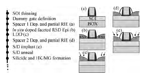
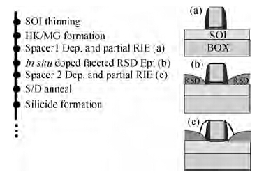
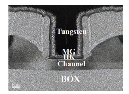
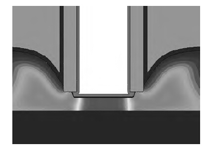
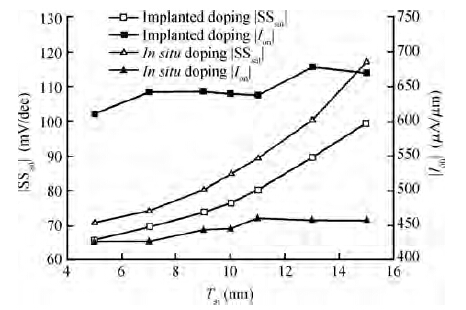
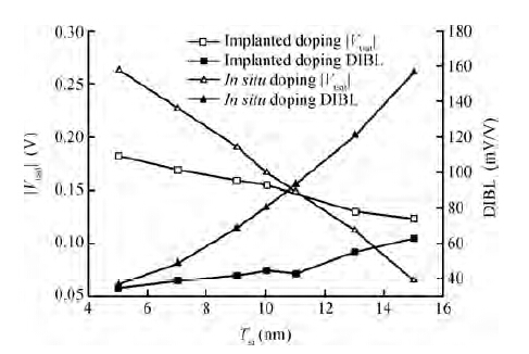
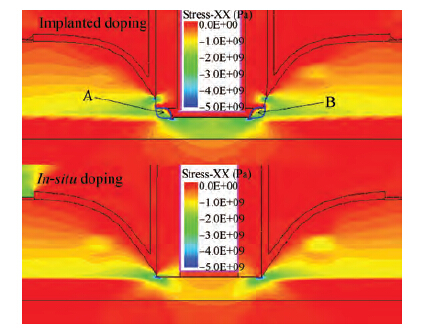
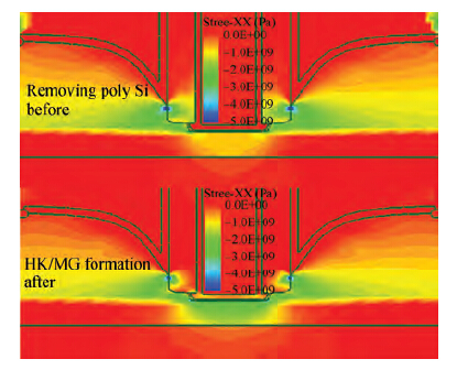
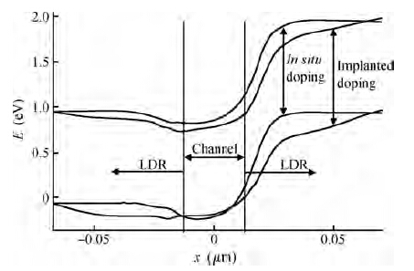
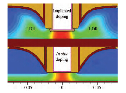
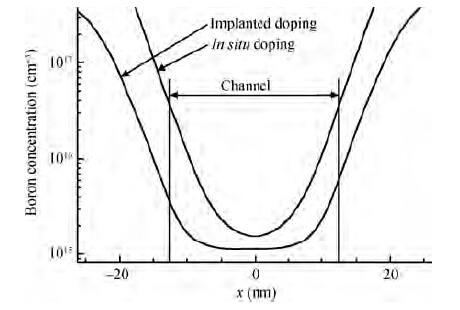
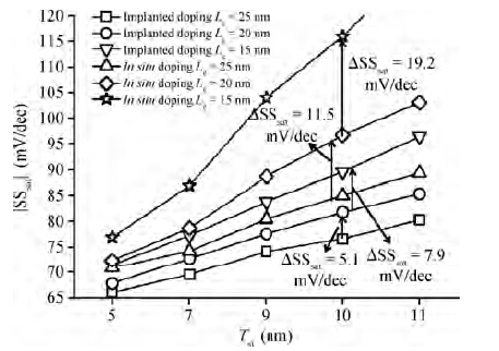
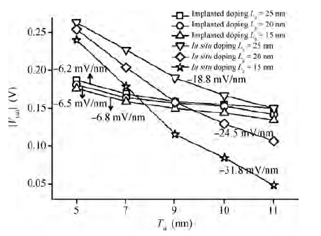
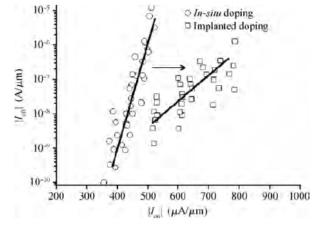
Extremely thin silicon on insulator p-channel metal-oxide-semiconductor field-effect transistors (PMOSFETs) with implanted doping and in situ doping are analyzed by TCAD simulation. The critical characteristic parameters acquired by TCAD simulation are compared with each other to analyze their electrical performance. The saturated driven currents of implanted doping devices with a 25 nm gate length (Lg) are about 200 μA/μm bigger than the in situ doping devices at the same saturated threshold voltage (Vtsat). Meanwhile the drain-induced barrier lowering (DIBL) and saturated subthreshold swings for implanted doping devices are also 30-50 mV/V and 6.3-9.1 mV/dec smaller than those of in situ doping devices at 25 nm Lg and a 9-11 nm thickness of SOI (Tsi), respectively. The shift of Vtsat with Tsi for in situ doping devices with 15 nm Lg is -31.8 mV/nm, whereas that for in situ doping devices is only -6.8 mV/nm. These outcomes indicate that the devices with implanted doping can produce a more advanced and stable electrical performance.