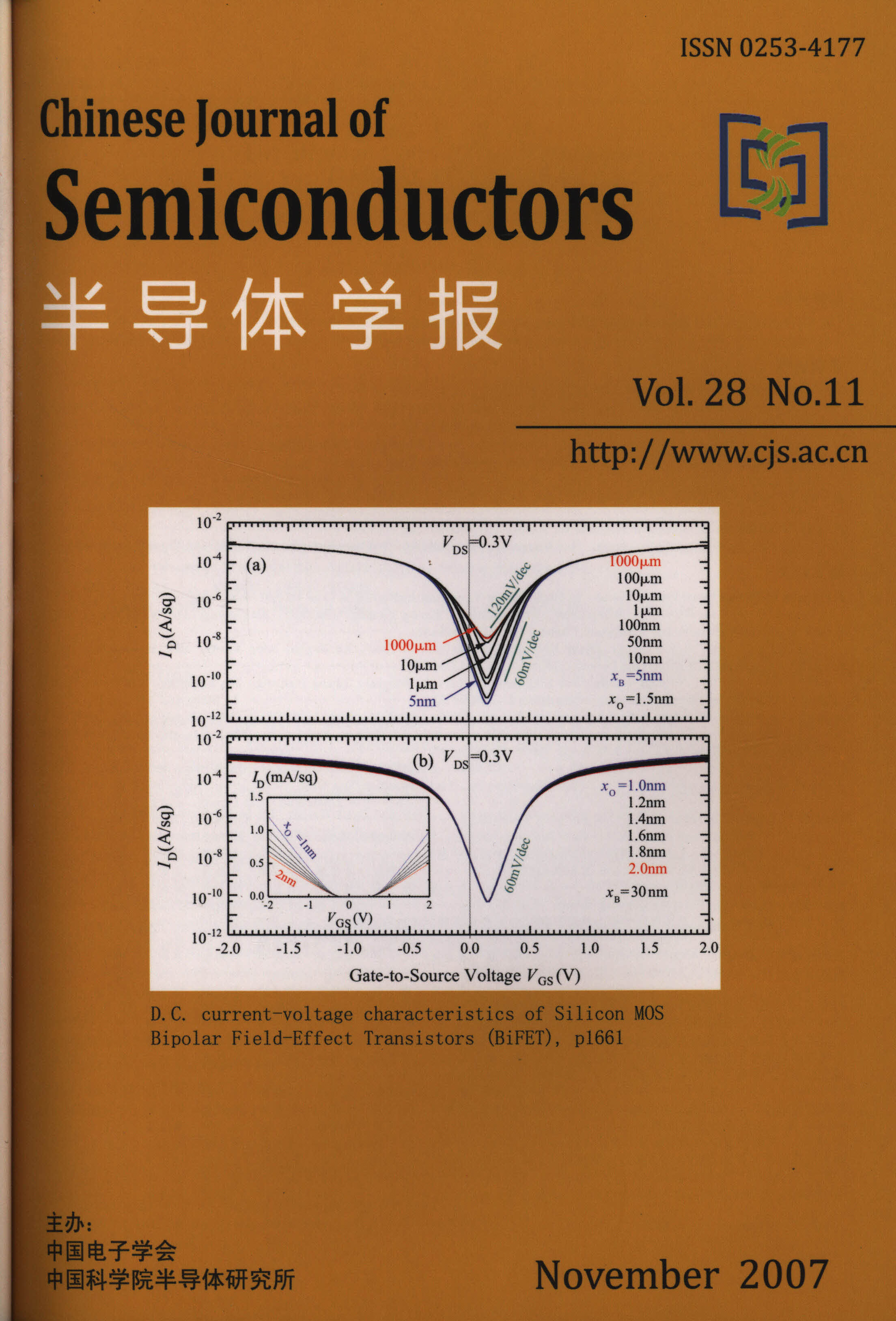
This paper describes the bipolar field-effect transistor (BiFET) and its theory.Analytical solution is obtained from partitioning the two-dimensional transistor into two one-dimensional transistors.The analysis employs the parametric surface-electric-potential and the electrochemical (quasi-Fermi) potential-gradient driving force to compute the current. Output and transfer D.C.current and conductance versus voltage are presented over practical ranges of terminal D.C.voltages and device parameters. Electron and hole surface channel currents are present simultaneously,a new feature which could provide circuit functions in one physical transistor such as the CMOS inverter and SRAM memory.
Issue Browser
Volume 28, Issue 11,
Nov 2007
Chin. J. Semicond.
2007, 28(11): 1661-1673
Chin. J. Semicond.
2007, 28(11): 1674-1678
We report on a GaN metal-oxide-semiconductor high electron mobility transistor (MOS-HEMT) using atomic-layer deposited (ALD) Al2O3 as the gate dielectric.Through decreasing the thickness of the gate oxide to 3.5nm,a device with maximum transconductance of 130mS/mm is produced.The drain current of this 1μm gate-length MOS-HEMT can reach 720mA/mm at +3.0V gate bias.The unity current gain cutoff frequency and maximum frequency of oscillation are obtained as 10.1 and 30.8GHz,respectively.
Chin. J. Semicond.
2007, 28(11): 1679-1684
A VDMOS integrated in a 170V scan-driver chip of a plasma display panel (PDP) is described,which is based on epitaxial bipolar-CMOS-DMOS (BCD) technology.Some key considerations and parameters of the design are discussed.The thickness of epitaxial layer is 17μm,the area of a single VDMOS structure cell is 324μm2,and only 18 photoetching steps are needed in the development process.It is also compatible with standard CMOS,bipolar,and p-LDMOS devices.The breakdown voltage of VDMOS in the process control module (PCM) is more than 200V.Five kinds of VDMOS modules are integrated in 64 channel PDP scan-driver IC,and on-line system verification is done on a LG-model-42v6 PDP.
Chin. J. Semicond.
2007, 28(11): 1685-1689
This paper presents a three-stage CMOS operational amplifier (opamp) that combines accuracy with stability for a wide range of capacitive loads.A so-called quenching capacitor is added to a multipath nested Miller compensation (MNMC) topology to obtain stability for a wide range of capacitive loads.Theoretical analysis and mathematical formulas are provided to prove the improvement in stability.A prototype of this frequency compensation scheme is implemented in a 0.7μm CMOS process.Measurements show that the amplifier can drive capacitive loads ranging from 100pF to 100μF with a gain of 90dB and a minimum phase margin of 26°.The amplifier has a unity-gain bandwidth of 1MHz for a 100pF capacitive load.It employs a quenching capacitance of 18pF.
Chin. J. Semicond.
2007, 28(11): 1690-1695
This paper presents a low-voltage low-power variable gain amplifier,which is applied in the automatic gain control loop of a super heterodyne receiver.Six stages are cascaded to provide an 81dB digitally controlled gain range in a 3dB step.The gain step error is less than 05dB.It operates at an intermediate frequency of 300kHz,and the power consumption is 1.35mW from a 1.8V supply.The prototype chip is implemented in a TSMC’s 0.18μm 1P6M CMOS process and occupies approximately 0.24mm2.It is very suitable for portable wireless communication systems.The measurement results agree well with the system requirements.
Chin. J. Semicond.
2007, 28(11): 1696-1700
This paper introduces a novel verification development platform for the passive UHF RFID tag,which is compatible with the ISO/IEC 18000-6B standard, operating in the 915MHz ISM band.This platform efficiently reduces the design and development time and cost,and implements a fast prototype design of the passive UHF RFID tag.It includes the RFID analog front end and the tag control logic,which is implemented in an Altera ACEX FPGA.The RFID analog front end,which is fabricated using a Chartered 0.35μm two-poly four-metal CMOS process,contains a local oscillator,power on reset circuit,matching network and backscatter,rectifier,regulator,AM demodulator,etc.The platform achieves rapid,flexible and efficient verification and development,and can also be fit for other RFID standards after changing the tag control logic in FPGA.
Chin. J. Semicond.
2007, 28(11): 1701-1705
The diffusion behavior of vanadium (V) implanted in SiC is investigated by secondary ion mass spectrometry.Significant redistribution,especially out-diffusion of vanadium towards the sample surface, is not observed after 1650℃ annealing.Higher carrier concentration is obtained due to a lack of compensation of vanadium in the surface region.The electrical characteristics of Ni contacts to V-implanted n-type 4H-SiC are investigated using a linear transmission line method.A specific contact resistance as low as 4.4e-3Ω·cm2 is achieved after annealing at 1050℃ for 10min in gas ambient consisting of 90% N2 and 10% H2.X-ray diffraction analysis shows the formation of Ni2Si and graphite phase at the interface after annealing.This provides the evidence that the carbon vacancies,resulting from the out-diffusion of carbon atoms from SiC,contribute to the formation of ohmic contact through the reduction of effective Schottky barrier height for the transport of electrons.
Chin. J. Semicond.
2007, 28(11): 1706-1711
A new method is used to simulate InGaAs/InP composite channel high electron mobility transistors (HEMTs).By coupling the hydrodynamic model and the density gradient model,the electron density distribution in the channel in different electric fields is obtained.This method is faster and more robust than traditional methods and should be applicable to other types of HEMTs simulations.A detailed study of the InGaAs/InP composite channel HEMTs is presented with the help of simulations.
Chin. J. Semicond.
2007, 28(11): 1712-1716
A continuous and analytical surface potential model for SOI LDMOS,which accounts for automatic transitions between fully and partially-depleted statuses,is presented.The surface potential equation of the SOI device is solved by using the PSP’s accurate algorithm of surface potential,and the front and back surface potentials are obtained analytically as a function of gate and drain voltage.The formulations of inversion charge and body charge under the fully-depleted state have been modified.The continuous and analytical DC model for SOI LDMOS is given based on PSP.The comparisons between simulation and measurements indicate that this model can predict the DC characteristics of SOI LDMOS accurately.
Chin. J. Semicond.
2007, 28(11): 1717-1721
A compact model for the integrated inversion charge density Qi in double-gate (DG-) MOSFETs is developed.For nanoscale applications,quantum confinement of the inversion carriers must be taken into account.Based on the previous work of Ge,we establish an expression for the surface potential with respect to Qi,and form an implicit equation,from which Qi can be solved.Results predicted by our model are compared to published data as well as results from Schred,a popular 1D numerical solver that solves the Poisson’s and Schrdinger equations self-consistently.Good agreement is obtained for a wide range of silicon layer thickness,confirming the superiority of this model over previous work in this field.
Chin. J. Semicond.
2007, 28(11): 1722-1728
The influence of the distribution of nano-pores on the mechanical properties evaluation of porous low-k films by surface acoustic waves (SAW) is studied.A theoretical SAW propagation model is set up to characterize the periodic porous dielectrics by transversely isotropic symmetry.The theoretical deductions of SAW propagating in the low-k film/Si substrate layered structure are given in detail.The dispersive characteristics of SAW in different propagation directions and the effects of the Young’s moduli E,E′ and shear modulus G′ of the films on these dispersive curves are found.Computational results show that E′ and G′ cannot be measured along the propagation direction that is perpendicular to the nano-pores’ direction.
Chin. J. Semicond.
2007, 28(11): 1729-1734
This paper presents a new quasi-static single-phase energy recovery logic (QSSERL), which unlike any other existing adiabatic logic family,uses a single sinusoidal supply-clock without additional timing control voltages.This not only ensures lower energy dissipation,but also simplifies the clock design,which would be otherwise more complicated due to the signal synchronization requirement.It is demonstrated that QSSERL circuits operate as fast as conventional two-phase energy recovery logic counterparts.Simulation with an 8bit logarithmic look-ahead adder (LLA) using static CMOS,clocked CMOS adiabatic logic (CAL,an existing typical single-phase energy recovery logic),and QSSERL,under 128 randomly generated input vectors,shows that the power consumption of the QSSERL adder is only 45% of that of the conventional static CMOS counterpart at 10MHz, and the QSSERL adder achieves better energy efficiency than CAL when the input frequency f input is larger than 2MHz.
Chin. J. Semicond.
2007, 28(11): 1735-1741
This paper presents an efficient way to implement an interpolation filter in a 20bit Σ-Δ DAC with an oversampling ratio of 128.A multistage structure is used to reduce the complexity of filter coefficients and the finite word length effect.A novel method based on mixed-radix number representation is proposed to realize a poly-phase multiplier-free half-band subfilter with a high resolution.This approach reduces the complexity of the control system and saves chip area dramatically.The IC is realized in a standard 0.13μm CMOS process and the interpolation filter occupies less than 0.63mm2.This realization has desirable properties of regularity with simple hardware devices which are suitable for VLSI and can be applied to many other high resolution data converters.
Chin. J. Semicond.
2007, 28(11): 1742-1747
A high voltage BCD process using thin epitaxial technology is developed for high voltage applications.Compared to conventional thick expitaxial technology,the thickness of the n-type epitaxial layer is reduced to 9μm,and the diffusion processing time needed for forming junction isolation diffusions is substantially reduced.The isolation diffusions have a smaller lateral extent and occupy less chip area.High voltage double RESURF LDMOS with a breakdown voltage of up to 900V,as well as low voltage CMOS and BJT,are achieved using this high voltage BCD compatible process.An experimental high voltage half bridge gate drive IC using a coupled level shift structure is also successfully implemented,and the high side floating offset voltage in the half bridge drive IC is 880V.The major features of this process for high voltage applications are also clearly demonstrated.
Chin. J. Semicond.
2007, 28(11): 1748-1755
Molecular dynamic simulations are performed to investigate the microscopic process when a Si atom with an incident energy of 0.03eV bombards a Si(001) 2×1 reconstructed surface at 300K using the Tersoff potential.Six different bombarding sites are chosen in order to study the interaction between the bombarding Si atom and substrate surface atoms.We map the bombarding Si atom’s kinetic energy,potential energy and trajectory.The results show that the interaction between the bombarding Si atom and the substrate surface atoms completes in a few picoseconds.The max binding energy of an adatom to a Si(001) 2×1 reconstructed surface is about 2.99eV.A single,0.03eV incident Si atom can open a surface dimer in dozens of femtoseconds after the interaction takes place from positions 5 or 6,while the atom bombarded from positions 1,2,3,4 cannot.
Chin. J. Semicond.
2007, 28(11): 1756-1760
High-quality c-axis oriented ZnO thin films are grown on Si(111) substrates at different substrate temperatures by pulsed laser deposition.Synchrotron radiation X-ray grazing incident diffraction (GID) is employed to study the interface structure of ZnO /Si(111).GID results indicate that there is a compressive stress in all ZnO epitaxial films grown at substrate temperatures of 500 or 300℃ by PLD.With the increase of X-ray detection depth,the compressive stress increases.Combined with conventional XRD technology,the biaxial stress,Possion’s ratio,and c/a of the ZnO films are calculated.The two samples have a six-sided closed packing structure,deviating from the value of the standard ZnO.This indicates that the sample grown at 500℃ has better crystal quality.
Chin. J. Semicond.
2007, 28(11): 1761-1764
By means of optical absorption,photoluminescence (PL),and ellipsometric spectra,metal organic chemical vapor deposition (MOCVD) grown InN films are investigated.Through absorption and PL measurements,it is proven that the band gap of the high quality InN is 0.68eV,which agrees with the recently reported value of ~0.7eV.By analysis of the Raman scattering spectrum,the comparatively low background concentration of electrons results in a smaller band gap value.The transition energy E0 of wurtzite InN at critical point Г0 is determined by ellipsometric spectra.In addition,the complex refractive index n+ik of InN in the energy range from 0.65 to 4.0eV is obtained for the first time.
Chin. J. Semicond.
2007, 28(11): 1765-1768
Heavily carbon doped p-type GaAsSb epi-layers with lattice matched to InP substrate are grown by gas source molecular beam epitaxy (GSMBE) using carbon tetrabromide (CBr4) as the carbon source.The doping characteristics of carbon-doped GaAsSb with a hole concentration of (1~20)e19cm-3 are investigated.A maximal hole concentration of 2.025e20cm-3 is obtained with a corresponding mobility of 20.4cm2/(V·s).The effects of growth temperature on the epi-layer composition,crystalline quality,and surface roughness are also studied experimentally,and it is found that 480℃ is the optimal growth temperature at which high quality carbon-doped p-type GaAsSb epi-layers can be obtained.
Chin. J. Semicond.
2007, 28(11): 1769-1772
The lifetime mapping of a p+-InP/n-InGaAs/n-InP double heterojunction wafer is measured by the microwave photoconductivity decay technique,and the mechanism of photoconductivity decay in this material is analyzed.Based on this analysis,the relationship between the measured lifetime and the device parameters is determined,and the abnormal change of lifetime with the decrease in temperature is explained.
Chin. J. Semicond.
2007, 28(11): 1773-1776
A high output power recessed AlGaN/GaN HEMT on SiC substrate is fabricated.With the optimized process,the specific contact resistance is less than 1.0e-6Ω·cm2,the current collapse parameter is less than 10%,and the breakdown voltage is more than 80V.For the short gate-wide device,the operation voltage is up to 40V,and the output power density is more than 10W/mm at 8GHz.For the single-cell device,the output power is 12.3W at 8GHz,the gain is 4.9dB,and the PAE is 35%.For the four-cell internally matched device with 8mm total-gate,33.8W output power is achieved at 8GHz,the gain is 6.3dB,and the PAE is 41.77%.The output power of single-cell and internally matched devices are currently the best in mainland China.
Chin. J. Semicond.
2007, 28(11): 1777-1781
The mechanism for increasing gate leakage current in recessed-gate AlGaN/GaN HEMTs,which are fabricated successfully by plasma dry etching,is investigated.Compared with conventional planar FETs,the gate leakage current of the recessed-gate AlGaN/GaN HEMTs increases by 10 times,and the breakdown voltage decreases to some extent.AFM and XPS are employed to measure the AlGaN surface before and after etching.The AlGaN surface becomes rougher,and even some protuberances like awl appear during dry etching.Thus the contact area between the metal and the semiconductor increases for the rougher AlGaN surface.On the other hand,some N vacancies generate plasma bombarding during dry etching.The N vacancies,which enhance the tunneling effect and reduce the Schottky barrier height,are regarded as n-type doped in the etched AlGaN surface.All these experiments indicate that the significant increase in the gate leakage current is due to the increased roughness and the appearance of these N vacancies in the AlGaN surface.
Chin. J. Semicond.
2007, 28(11): 1782-1785
An n-channel field-effect-transistor (FFET) with a metal/ferroelectric/metal/insulator/Si substrates (MFMIS) structure is fabricated by using a Pb(Zr0.52Ti0.48)O3 (PZT) thin film of the preferential orientation of (111) on Si substrates prepared by the RF magnetron sputtering technique integrated with semiconductor technology.TheC-V characteristics,I-V characteristics,and data writing speed of the FFET are investigated.The clockwise C-V and counterclockwise Id-Vg hysteresis loops of the n-channel FFET demonstrate that the FFET could realize a memory effect due to the ferroelectric polarization of PZT thin film.The memory window of the FFET is 2V,observed from the C-V and Id-Vg hysteresis curves with Vg swinging between -5 and +5V.
Chin. J. Semicond.
2007, 28(11): 1786-1793
An accuracy large-signal equivalent circuit model of radio frequency silicon-on-insulator (RF-SOI) lateral double diffused MOSFET (LDMOSFET) with body-contact is presented.Both the equations for channel current and bias-dependence capacitors modeling are continuous and high order drivable.A new charge conservative expression is developed.The bias dependences of the drift resistor,parasitic resistor,and capacitor under the lightly doped drain region are considered.The power dissipation caused by self-heating and the frequency distribution of the transconductor are described.The model is finally used to construct a 20-gate-fingers (channel mask length,L=1μm,finger width,W=50μm) RF-SOI LDMOSFET on high resistivity SOI with body-contact device modeling.Comparison results of the measured and simulated DC,S-parameters,and power characteristics are supplied to demonstrate the excellent accuracy of the model.
Chin. J. Semicond.
2007, 28(11): 1794-1802
Eight node capacitance models are presented to generate the model library.It is proved that these models can be used to extract the capacitances from almost all of the VLSI interconnect structures.The formula for each model is also given.The numerical results show that our method is accurate.For the results obtained by formulas,it is also very fast.
Chin. J. Semicond.
2007, 28(11): 1803-1806
The fabrication process of 980nm,densely packed,high power,VCSEL 2D-arrays is reported for the first time in mainland China.The individual elements of the arrays are arranged in a honeycomb-like layout,the mesa diameter of the element is 70μm,the oxide aperture is 30μm,and the center-to-center spacing of neighboring elements is 100μm.VCSEL arrays containing 7,19,and 37 elements are fabricated,and the characteristics of the threshold current and the far-field angle are discussed.Given CW operation at room temperature,these three kinds of arrays have 0.26,0.5,and 0.6W output power,respectively.With a 6A pulse current (30μs at 100Hz),the 37-elements array’s output power reaches 1.4W.
Chin. J. Semicond.
2007, 28(11): 1807-1810
We demonstrate a tunable long-wavelength photodetector by using a heteroepitaxy growth of an InP-In0.53Ga0.47-As-InP p-i-n structure on a GaAs-based GaAs/AlAs Fabry-Perot filter structure.High quality heteroepitaxy is realized by employing a thin low-temperature buffer layer,which is carried out in a series of experiments.A wavelength tuning range of 10.0nm,an external quantum efficiency of about 23%,a spectral linewidth of 0.8nm,and a 3dB bandwidth of 6.2GHz are simultaneously obtained in the device.
Chin. J. Semicond.
2007, 28(11): 1811-1814
Three different solutions [dilute HCl,(NH4)2S,and aqua regia] are used to treat a p-GaN surface,and bi-layer Ni/Au films are used as ohmic contacts to p-GaN.XPS spectra show that the (NH4)2S and aqua regia are more effective in removing the native oxide of the p-GaN than the dilute HCl.By comparing and analyzing I-V characteristics,the specific contact resistances,and the relative Ga/N atomic concentration ratio on p-type GaN surfaces of these samples,we concluded that there are more Ga vacancies in the aqua regia treated p-GaN surface and a higher ohmic contact performance can be obtained.
Chin. J. Semicond.
2007, 28(11): 1815-1817
n-GaAs and p-GaN wafer pairs are successfully bonded by direct wafer bonding technology.SEM results indicate that there is no bonding gap at the bonding interface.PL measurements indicate that the bonding process does not visibly change the crystal quality.The current-voltage characteristics at room temperature show that the bonded n-GaAs/p-GaN heterojunction is a Shockley diode and the ideality factor n is 1.08.This high quality bonded wafer of n-GaAs/p-GaN has great implications for the optoelectronic integration of GaAs and GaN semiconductor materials.
Chin. J. Semicond.
2007, 28(11): 1818-1823
A novel p-type Domino AND gate utilizing the sleep transistor,dual threshold voltage,and source following evaluation gate (SEPG) techniques is proposed.HSPICE simulation results prove that the leakage current of the proposed design can be reduced by 43%,62%,and 67% while improving the noise margin 3.4%,23.6%,and 13.7% when compared to standard dual Vt Dominos,standard low Vt dominos,and the SEFG structure under similar delay time,respectively.Therefore,the proposed Dominos AND gate solves the high leakage current and deteriorated robustness problem in sub-65nm CMOS technologies.Finally,the inputs and clock signals combination sleep state dependent on leakage current characteristics is analyzed,and the optimal sleep state is obtained.
Chin. J. Semicond.
2007, 28(11): 1824-1829
A high accuracy temperature sensor is designed by applying the temperature characteristics of a substrate bipolar transistor in CMOS technology.The use of dynamic element matching enables us to solve problems caused by IC technology mismatching.Simulated results using CSMC 0.5μm mixed signal technology show that the accuracy is 0.15℃ and the linearity is 0.15%.Measured results of several different chips show that the accuracy is within 0.6℃ and the linearity is within 0.68%.The power dissipation is 587μW and the chip area is 225μm×95μm.The output is an analog voltage signal,which is easy to collect,process,and apply.
Chin. J. Semicond.
2007, 28(11): 1830-1835
The design,fabrication,and test results of a 2D thermal wind sensor are presented.The wind sensor measures wind speed and direction by calorimetric principle in constant power mode.Heater and detector resistors are fabricated on glass substrate using a lift-off process.The fabrication is simple and reliable,and good thermal isolation and high sensitivity are achieved.The sensor can detect wind speed in the range of 10m/s and flow direction over 360° with an error of less than 8°.The response time of the sensor is less than 1s,and the heat power is 10mW.
Chin. J. Semicond.
2007, 28(11): 1836-1843
This paper presents a novel low noise,low power fully digitally controlled LC oscillator (DCO) for PHS transceivers in an SMIC 0.18μm CMOS process.To improve the performance of the DCO,several circuit techniques,such as inversion-mode digitally controlled MOS varactors,a digitally controlled MOS varactor matrix,dynamic element matching,and a lined MASH ΣΔ modulator,are used.The measured phase noise of this DCO at 100kHz offset frequency at 3.1GHz is below -102.3 and down to -122.6dBc/Hz at 1.2MHz while drawing 2.8mA of current from a 1.8V supply.Compared with state of the art DCOs,the measurement results demonstrate that our DCO features superior phase noise and power consumption.